JP3639602B2 - Liquid crystal display - Google Patents
Liquid crystal display Download PDFInfo
- Publication number
- JP3639602B2 JP3639602B2 JP51195399A JP51195399A JP3639602B2 JP 3639602 B2 JP3639602 B2 JP 3639602B2 JP 51195399 A JP51195399 A JP 51195399A JP 51195399 A JP51195399 A JP 51195399A JP 3639602 B2 JP3639602 B2 JP 3639602B2
- Authority
- JP
- Japan
- Prior art keywords
- liquid crystal
- crystal display
- circuit board
- notch
- display device
- Prior art date
- Legal status (The legal status is an assumption and is not a legal conclusion. Google has not performed a legal analysis and makes no representation as to the accuracy of the status listed.)
- Expired - Fee Related
Links
Images








Classifications
-
- G—PHYSICS
- G02—OPTICS
- G02F—OPTICAL DEVICES OR ARRANGEMENTS FOR THE CONTROL OF LIGHT BY MODIFICATION OF THE OPTICAL PROPERTIES OF THE MEDIA OF THE ELEMENTS INVOLVED THEREIN; NON-LINEAR OPTICS; FREQUENCY-CHANGING OF LIGHT; OPTICAL LOGIC ELEMENTS; OPTICAL ANALOGUE/DIGITAL CONVERTERS
- G02F1/00—Devices or arrangements for the control of the intensity, colour, phase, polarisation or direction of light arriving from an independent light source, e.g. switching, gating or modulating; Non-linear optics
- G02F1/01—Devices or arrangements for the control of the intensity, colour, phase, polarisation or direction of light arriving from an independent light source, e.g. switching, gating or modulating; Non-linear optics for the control of the intensity, phase, polarisation or colour
- G02F1/13—Devices or arrangements for the control of the intensity, colour, phase, polarisation or direction of light arriving from an independent light source, e.g. switching, gating or modulating; Non-linear optics for the control of the intensity, phase, polarisation or colour based on liquid crystals, e.g. single liquid crystal display cells
- G02F1/133—Constructional arrangements; Operation of liquid crystal cells; Circuit arrangements
- G02F1/1333—Constructional arrangements; Manufacturing methods
- G02F1/133308—Support structures for LCD panels, e.g. frames or bezels
-
- G—PHYSICS
- G02—OPTICS
- G02F—OPTICAL DEVICES OR ARRANGEMENTS FOR THE CONTROL OF LIGHT BY MODIFICATION OF THE OPTICAL PROPERTIES OF THE MEDIA OF THE ELEMENTS INVOLVED THEREIN; NON-LINEAR OPTICS; FREQUENCY-CHANGING OF LIGHT; OPTICAL LOGIC ELEMENTS; OPTICAL ANALOGUE/DIGITAL CONVERTERS
- G02F1/00—Devices or arrangements for the control of the intensity, colour, phase, polarisation or direction of light arriving from an independent light source, e.g. switching, gating or modulating; Non-linear optics
- G02F1/01—Devices or arrangements for the control of the intensity, colour, phase, polarisation or direction of light arriving from an independent light source, e.g. switching, gating or modulating; Non-linear optics for the control of the intensity, phase, polarisation or colour
- G02F1/13—Devices or arrangements for the control of the intensity, colour, phase, polarisation or direction of light arriving from an independent light source, e.g. switching, gating or modulating; Non-linear optics for the control of the intensity, phase, polarisation or colour based on liquid crystals, e.g. single liquid crystal display cells
- G02F1/133—Constructional arrangements; Operation of liquid crystal cells; Circuit arrangements
- G02F1/1333—Constructional arrangements; Manufacturing methods
- G02F1/133308—Support structures for LCD panels, e.g. frames or bezels
- G02F1/13332—Front frames
-
- G—PHYSICS
- G02—OPTICS
- G02F—OPTICAL DEVICES OR ARRANGEMENTS FOR THE CONTROL OF LIGHT BY MODIFICATION OF THE OPTICAL PROPERTIES OF THE MEDIA OF THE ELEMENTS INVOLVED THEREIN; NON-LINEAR OPTICS; FREQUENCY-CHANGING OF LIGHT; OPTICAL LOGIC ELEMENTS; OPTICAL ANALOGUE/DIGITAL CONVERTERS
- G02F1/00—Devices or arrangements for the control of the intensity, colour, phase, polarisation or direction of light arriving from an independent light source, e.g. switching, gating or modulating; Non-linear optics
- G02F1/01—Devices or arrangements for the control of the intensity, colour, phase, polarisation or direction of light arriving from an independent light source, e.g. switching, gating or modulating; Non-linear optics for the control of the intensity, phase, polarisation or colour
- G02F1/13—Devices or arrangements for the control of the intensity, colour, phase, polarisation or direction of light arriving from an independent light source, e.g. switching, gating or modulating; Non-linear optics for the control of the intensity, phase, polarisation or colour based on liquid crystals, e.g. single liquid crystal display cells
- G02F1/133—Constructional arrangements; Operation of liquid crystal cells; Circuit arrangements
- G02F1/1333—Constructional arrangements; Manufacturing methods
- G02F1/133308—Support structures for LCD panels, e.g. frames or bezels
- G02F1/133328—Segmented frames
-
- G—PHYSICS
- G02—OPTICS
- G02F—OPTICAL DEVICES OR ARRANGEMENTS FOR THE CONTROL OF LIGHT BY MODIFICATION OF THE OPTICAL PROPERTIES OF THE MEDIA OF THE ELEMENTS INVOLVED THEREIN; NON-LINEAR OPTICS; FREQUENCY-CHANGING OF LIGHT; OPTICAL LOGIC ELEMENTS; OPTICAL ANALOGUE/DIGITAL CONVERTERS
- G02F1/00—Devices or arrangements for the control of the intensity, colour, phase, polarisation or direction of light arriving from an independent light source, e.g. switching, gating or modulating; Non-linear optics
- G02F1/01—Devices or arrangements for the control of the intensity, colour, phase, polarisation or direction of light arriving from an independent light source, e.g. switching, gating or modulating; Non-linear optics for the control of the intensity, phase, polarisation or colour
- G02F1/13—Devices or arrangements for the control of the intensity, colour, phase, polarisation or direction of light arriving from an independent light source, e.g. switching, gating or modulating; Non-linear optics for the control of the intensity, phase, polarisation or colour based on liquid crystals, e.g. single liquid crystal display cells
- G02F1/133—Constructional arrangements; Operation of liquid crystal cells; Circuit arrangements
- G02F1/1333—Constructional arrangements; Manufacturing methods
- G02F1/1345—Conductors connecting electrodes to cell terminals
- G02F1/13452—Conductors connecting driver circuitry and terminals of panels
-
- G—PHYSICS
- G02—OPTICS
- G02F—OPTICAL DEVICES OR ARRANGEMENTS FOR THE CONTROL OF LIGHT BY MODIFICATION OF THE OPTICAL PROPERTIES OF THE MEDIA OF THE ELEMENTS INVOLVED THEREIN; NON-LINEAR OPTICS; FREQUENCY-CHANGING OF LIGHT; OPTICAL LOGIC ELEMENTS; OPTICAL ANALOGUE/DIGITAL CONVERTERS
- G02F2201/00—Constructional arrangements not provided for in groups G02F1/00 - G02F7/00
- G02F2201/46—Fixing elements
- G02F2201/465—Snap -fit
Landscapes
- Physics & Mathematics (AREA)
- Nonlinear Science (AREA)
- Mathematical Physics (AREA)
- Chemical & Material Sciences (AREA)
- Crystallography & Structural Chemistry (AREA)
- General Physics & Mathematics (AREA)
- Optics & Photonics (AREA)
- Liquid Crystal (AREA)
Description
[技術分野]
本発明は、液晶表示パネルと、駆動回路基板等を有する液晶表示装置(すなわち、液晶表示モジュール)に関する。
[背景技術]
例えばアクティブ・マトリクス方式の液晶表示装置の液晶表示素子では、液晶層を介して互いに対向配置されるガラス等からなる2枚の透明絶縁基板のうち、その一方のガラス基板の液晶層側の面に、そのx方向に延在し、y方向に並設されるゲート線群と、このゲート線群と絶縁されてy方向に延在し、x方向に並設されるドレイン線群とが形成されている。
これらのゲート線群とドレイン線群とで囲まれた各領域がそれぞれ画素領域となり、この画素領域にスイッチング素子として例えば薄膜トランジスタ(TFT)と透明画素電極とが形成されている。
ゲート線に走査信号が供給されることにより、薄膜トランジスタがオンされ、このオンされた薄膜トランジスタを介してドレイン線からの映像信号が画素電極に供給される。
なお、ドレイン線群の各ドレイン線はもちろんのこと、ゲート線群の各ゲート線においても、それぞれ透明絶縁基板の周辺にまで延在されて外部端子を構成し、この外部端子にそれぞれ接続されて映像駆動回路、ゲート走査駆動回路、すなわち、これらを構成する複数個の駆動IC(半導体集積回路)が該透明絶縁基板の周辺に外付けされるようになっている。つまり、これらの各駆動ICを搭載したテープキャリアパッケージ(TCP)を基板の周辺に複数個外付けする。
しかし、このように透明絶縁基板は、その周辺に駆動ICが搭載されたTCPが外付けされる構成となっているので、これらの回路によって、透明絶縁基板のゲート線群とドレイン線群との交差領域によって構成される表示領域の輪郭と、該透明絶縁基板の外枠の輪郭との間の領域(通常、額縁と称している)の占める面積が大きくなってしまい、液晶表示モジュールの外形寸法を小さくしたいという要望に反する。
それゆえ、このような問題を少しでも解消するために、すなわち、液晶表示素子の高密度化と液晶表示モジュールの外形をできる限り縮小したいとの要求から、TCP部品を使用せず、映像駆動ICおよびゲート走査駆動ICを透明絶縁基板上に直接搭載する構成が提案された。このような実装方式をフリップチップ方式、あるいはチップ・オン・ガラス(COG)方式という。
また、フリップチップ方式の液晶表示装置に関しては、例えば同一出願人による特開平8−122806号公報に記載されている。
[発明の開示]
従来の技術では、液晶表示装置の表示に寄与しない領域、所謂額縁領域、を小さくした場合の、液晶表示装置の機械的な衝撃に対する強度についての検討が不十分であったため、液晶表示装置の額縁領域を小さくすることに限界があった。
また、液晶表示装置の所謂額縁領域を小さくした場合に、バックライトの導光体の光入射面近辺で発生するバックライトの輝度むらが表示画面に輝線となって見える問題についての対策が不十分であったため、液晶表示装置の額縁領域を小さくすることの妨げになっていた。
本発明は、液晶表示装置の額縁領域を小さくした場合に生じる問題を解決し、表示画面が大きくかつコンパクトな液晶表示装置を提供することを主たる目的とする。
液晶表示装置の表示に寄与しない領域、所謂額縁領域、を小さくすると、取り付け穴の形状も従来の丸穴から、U字形の切り欠きに変える必要が出てくる。
しかし従来のU字形の切り欠きは、機械的なストレスや衝撃を強く加えると、変形しやすい。取り付け部の切り欠きが変形すると、液晶表示パネル(液晶表示素子)の変形や、液晶表示パネルの割れが起こる。
本発明の一つの目的は、液晶表示装置の取り付け部の変形を防止することにある。
液晶表示装置の取り付け部の変形を防止する為に、本発明では、液晶表示素子と、該液晶表示素子の表示部を露出する開口を有し上記液晶素子の周囲を覆う上側ケースと、上記上側ケースと合体し上記液晶素子を収納する下側ケースとを有する液晶表示装置であって、該液晶表示装置を固定するための切り欠きを上記液晶表示装置の周辺に設け、上記切り欠きは上記上側ケースに形成した第1の切り欠きと下側ケースに形成した第2の切り欠きを重ね合せて形成され、上記切り欠きに略平行で、上記切り欠きに最も近い側の側面の上記上側ケースをL字形に折り曲げたことを特徴とする。
また、液晶表示素子と、該液晶表示素子の表示部を露出する開口を有し上記液晶素子の周囲を覆う上側ケースと、上記上側ケースと合体し上記液晶素子を収納する下側ケースとを有する液晶表示装置であって、該液晶表示装置を固定するための切り欠きを上記液晶表示装置の周辺に設け、上記切り欠きは上記上側ケースに形成した第1の切り欠きと下側ケースに形成した第2の切り欠きを重ね合せて形成され、上記切り欠きに略平行で、上記切り欠きに最も近い側の側面の上記下側ケースをL字形に折り曲げたことを特徴とする。
さらには、液晶表示素子と、該液晶表示素子の表示部を露出する開口を有し上記液晶素子の周囲を覆う上側ケースと、上記上側ケースと合体し上記液晶表示を収納する下側ケースとを有する液晶表示装置であって、該液晶表示装置を固定するための切り欠きを上記液晶表示装置の周辺に設け、上記切り欠きは上記上側ケースに形成した第1の切り欠きと下側ケースに形成した第2の切り欠きを重ね合せて形成され、上記切り欠きに略平行で、上記切り欠きに最も近い側の側面の上記上側ケース及び上記下側ケースをL字形に折り曲げたことを特徴とする。
上記構成によれば、Fig.21A及び21Bに示すように、上側ケースSHDと下側ケースLFをモールドMLの外側にL字に曲げて配置することにより、y、y'方向の衝撃を、モールドML、上側ケースSHDの上面1a、下側ケースLFの上面2aだけでなく、上側ケースSHDの側面1b及び又は下側ケースLFの側面2bで受け止めることが出来るので、U字形切り欠きが変形し難くなる。
また、額縁領域を小さくすると、上側ケースの開口部が大きくなる。
しかし、バックライトの導光板よりも上側ケースの開口が大きくなると、液晶表示装置に機械的に強い衝撃が加わった時に、導光板と上側ケースに挟まれた液晶表示パネルに、導光板が衝突し、せん断応力が生じ、液晶表示パネルの基板が割れるため、従来の技術では額縁領域を小さくすることが困難であった。
本発明の他の目的は、液晶表示装置の上側ケースの開口部を大きくしても、液晶表示パネルの基板が割れない構造を提供することにある。
液晶表示パネルの基板が割れるのを防止する為に、本発明では、液晶表示素子と、該液晶表示素子に重なり上記液晶表示素子に光を照射する導光板と、上記液晶表示素子の表示部を露出する開口を有し上記液晶素子の周囲を覆う上側ケースと、上記上側ケースと合体し上記液晶素子及び上記導光板を収納する下側ケースとを有する液晶表示装置であって、上記導光板は対向する2辺を有し、上記導光板の対向する2辺の夫々の辺の中央付近に、上記上側ケースと平面的に重なる突起を設けたことを特徴とする。
本発明によれば、Fig.22A及び22Bに示すように、導光板GLBの辺の中央付近に突起4aを上側ケースSHDに重なるように配置しているので、液晶表示装置に強い衝撃が加わった時に、導光板GLBの変形が突起4aにより押さえられ、液晶表示パネルPNLにせん断応力が加わることがない。
従って本発明によれば、液晶表示装置の衝撃に対する強度を強くすることが出来る。
また液晶表示装置の額縁領域を小さくすると、導光板に蛍光管から光が入射する入光面が液晶表示パネルの表示領域に近くなり、導光板の入光部で発生する輝線や暗線などの輝度むらが表面画面に影響を及ぼす現象も、従来技術では十分に検討されていなかった。
発明者らの研究によれば、従来導光板の入光部には蛍光管の光を反射するランプ反射シートや、導光板の反射面に設けられる反射シートや、導光板の光射出面に設けられる拡散シートなど各種の光学シートが、両面粘着テープや接着剤あるいは溶融等により、導光板に固定されていた。
しかし、これら両面粘着テープや接着剤あるいは溶融等により、各種光学シートが導光板に固定された部分に、蛍光管の光が当たると、光が不規則に散乱され、バックライトの輝度むらを生じ、輝線が発生した。
バックライトの輝線を低減する方法としては、導光板の入光部近辺の反射シートや拡散シートに黒色または灰色の模様を印刷して光を吸収させる方法があるが、光の吸収量が多い場合は暗線が発生したり、吸収される光の分だけ余計に蛍光管の輝度を上げる必要があったため、バックライトの消費電力が大きくなる短所があった。
本発明の他の目的は、液晶表示装置の額縁領域を小さくした場合に、バックライトの導光体の光入射面近辺で発生するバックライトの輝度むらが表示画面に輝線や暗線となって見える問題を解決することにある。
上記問題を解決するために本発明では、液晶表示素子と、該液晶表示素子に重なり上記液晶表示素子に光を照射する導光板と、該導光板の上記液晶表示素子に光を照射する部分に開口を有し上記液晶表示素子と上記導光板の間に設けられる枠体と、上記液晶表示素子の表示部を露出する開口を有し上記液晶素子の周囲を覆う上側ケースと、上記上側ケースと合体し上記液晶素子、上記枠体及び上記導光板を収納する下側ケースとを有する液晶表示装置であって、
上記導光板の一つの側面に光源を配置し、上記光源を、上記導光体と対向する部分を除いて、光を反射するフィルムからなる第1の反射シートで覆い、該反射シートを上記枠体に固定したことを特徴とする。
また上記液晶表示素子と上記導光板の間に透過する光を拡散させる拡散シートを設け、該拡散シートを上記導光体の上記一つの側面に対向する側面の近傍で固定したことを特徴とする。
また上記導光板と上記下側ケースの間に光を反射するフィルムからなる第2の反射シートを設け、該第2の反射シートを上記導光体の上記一つの側面に対向する側面の近傍で固定したことを特徴とする。
本発明によれば、第1の反射シート、第2の反射シート及び拡散シートなどの光学シートを、導光板の入光部に両面粘着テープや接着剤あるいは溶融などにより固定していないので、導光板の入光部でバックライトの輝度むらが発生することがない。
すなわち本発明では、Fig.23に示すように、拡散シートSPS及び反射シートRFSを、導光板GLBの入光部と反対側で、導光板に両面粘着テープBAT等の固定部材で固定し、ランプ反射シートLSを、ランプ反射シートLSの非反射面5で,モールドML(枠体)に両面粘着テープBAT等の固定部剤で固定しているので、導光板の入光部に蛍光管LPの光が散乱される部分が無く、輝線や暗線などのバックライトの輝度むらを生じることがない。
従って本発明によれば、液晶表示装置の表示品質を向上することが出来る。
【図面の簡単な説明】
Fig.1Aは液晶モジュールの表示側から見た正面図、Fig.1Bは左側面図、Fig.1Cは右側面図、Fig.1Dは後側面図、Fig.1Eは前側面図である。
Fig.2Aはモジュールの裏面図、Fig.2BはFig.2AのB−B切断線断面図、Fig.2CはFig.2AのC−C切断線断面図である。
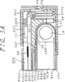
Fig.3AはFig.1Aに示す液晶表示装置のI−I切断線断面図、Fig.3BはFig.1AのII−II切断線断面図である。
Fig.4AはFig.1AのIII−III切断線断面図、Fig.4BはFig.1AのIV−IV切断線断面図である。
Fig.5は下側から見た枠状保持体MLとそれに収納されるバックライトおよびインターフェイス回路基板PCB等を示す全体分解斜視図である。
Fig.6Aはゲート側多層フレキシブル回路基板FPC1と、ドレイン側多層フレキシブル回路基板FPC2と、液晶パネルPNLの正面図、Fig.6Bは右側面図、Fig.6CはFig.6AのI−I切断線断面図である。
Fig.7A〜7CはFig.6A〜6Cに対応する比較例を示す図である。
Fig.8Aはドレイン側多層フレキシブル回路基板FPC2の正面図、Fig.8Bは左側面図、Fig.8Cは右側面図、Fig.8Dは端子の中心位置J1に対応する部分の拡大正面図、Fig.8Eは端子の中心位置J2〜J11に対応する部分の拡大正面図、Fig.8Fは端子の中心位置J12に対応する部分の拡大正面図である。
Fig.9Aはゲート側多層フレキシブル回路基板FPC1の正面図、Fig.9BはFig.9AのI−I切断線断面図である。
Fig.10Aはインターフェイス回路基板PCBの裏(下)面図、Fig.10Bは該回路基板PCBの正(上)面図である。
Fig.11はモジュールの各ドライバの概略構成と、信号の流れを示すブロック図である。
Fig.12はFig.11に対応する比較例を示す図である。
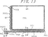
Fig.13はドレイン側回路基板FPC2をパネルPNLに取り付け後、折り返していない状態を示すFig.6Aと同様の図である。
Fig.14はFig.13において、ドレイン側回路基板FPC2をパネルPNLに取り付け折り返し、回路基板PCBにコネクタCT4を挿入しない状態を示す図である。
Fig.15A、15B、15CはFig.13、14の回路基板FPC2の折り曲げ方を示す側面図である。
Fig.16A〜16CはコネクタCT4を設けた回路基板FPC2の凸部を含めたFig.15A〜15Cと同様の図である。
Fig.17A〜17Dは上側金属製シールドケースSHDの4個の角部を示す斜視図、Fig.17E〜17Hは下側金属性シールドケースLFの4個の角部を示す斜視図である。
Fig.18Aは本例の回路基板PCBの面付け状態を示す平面図、Fig.18Bは本例の分割後の回路基板PCBの要部平面図、Fig.18Cは比較例の回路基板PCBの面付け状態を示す平面図、Fig.18Dは比較例の分割後の回路基板PCBの要部平面図である。
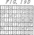
Fig.19Aは、集積回路素子TCONの下面図、Fig.19Bは側面図、Fig.19Cは集積回路TCONの下面の本例のピン配列の概略を示す図、Fig.19Dは比較例のピン配列の概略を示す図である。
Fig.20はゲート側多層フレキシブル懐炉基板FPC1とそれに重ねて配置されたインターフェイス回路基板PCBを示す要部斜視図である。
Fig.21Aは本発明の液晶表示装置を固定するための切り欠きの構造を示すための平面図、Fig.21Bは切り欠きの側面図である。
Fig.22Aは本発明の、導光板に設けた突起と、上側ケースの位置関係を示す平面図、Fig.22BはFig.22AのI−I線で切った断面図である。
Fig.23は本発明の、ランプ反射シート、拡散シート及び反射シートの固定方法を示す断面図である。
Fig.24は液晶表示装置全体の等価回路を示すブロック図である。
Fig.25はTFT液晶表示素子TFT−LCDの駆動波形を示す図である。
[発明を実施するための最良の形態]
以下、図面を用いて本発明の実施の形態について詳細に説明する。なお、以下で説明する図面で、同一機能を有するものは同一符号を付け、その繰返しの説明は省略する。
《液晶表示モジュールの全体構成》
Fig.1Aは液晶表示モジュールの組立完成後の表示側から見た正面図、Fig.1Bは左側面図、Fig.1Cは右側面図、Fig.1Dは後側面図、Fig.1Eは前側面図である。
Fig.1において、SHDは金属板からなる上側金属製シールドケース、WDは表示窓、PNLは重ね合わせた2枚の透明絶縁基板の一方の基板上に駆動ICを搭載してなるフリップチップ方式液晶表示パネル(液晶表示素子やLCD(リキッド クリスタル ディスプレイ)とも称す)、ARは有効画素エリア、HLD1〜4は該モジュールのパソコン等への取付穴または切り欠き、LPC1、LPC2はバックライトの蛍光管のランプケーブル、LCTはインバータとの接続コネクタである。
Fig.2Aは液晶表示モジュールの組立完成後の裏面図、Fig.2BはFig.2AのB−B切断線における断面図、Fig.2Cはフレームグランド部を示す要部断面図である。
Fig.2Aにおいて、LFは金属板からなる下側金属製シールドケース、DRHはシールドケースLFの下(底)面に貫通する複数個の穴、DRWは複数個の穴DRHの回りの凹み(Fig.2B参照)、Fig.GHはフレームグランド穴、SUPはコネクタCT4(Fig.8、6参照)を下から支持する凹み、CT1はインターフェイスコネクタ、HLD1〜4は該モジュールのパソコン等への取付穴である。
Fig.1、2において、両ケースSHD、LFにそれぞれ設けた4個の取付穴または切り欠きHLD1〜4は、当該モジュールを表示部としてパソコン、ワープロ等の情報処理装置にねじ等を用いて実装するための穴または切り欠き(HLD2とHLD4は閉じた穴ではなく切り欠き)である。両者に設けた取付穴または切り欠きHLD1〜4にねじ等を通して情報処理装置に固定、実装する。本体コンピュータ(ホスト)からの信号と必要な電源は、モジュール裏面に位置するインターフェイスコネクタCT1を介して、モジュール内のインターフェイス回路基板のコントローラ部および電源部に供給する。
以下、各構成部品の具体的な構成をFig.1〜Fig.20に示し、各部材について詳しく説明する。
《上側金属製シールドケースSHDと下側金属製シールドケースLF》
Fig.1Aに上側シールドケースSHDの上面、Fig.1B、1C、1Dに上側シールドケースSHDの各側面が示され、Fig.2Aに下側シールドケースLFの下面が示される。
メタルフレームとも称されるシールドケースSHD、LFは、1枚の金属板をプレス加工技術により、抜き打ちと折り曲げ加工により作製される。WDは液晶表示パネルPNLを視野に露出させる開口である表示窓である。ケースSHDは、厚さ0.4mmのステンレス板(強度大)からなり、ケースLFは、厚さ0.3mmのアルミ板からなる。
Fig.2Aに示すように、下側金属製シールドケースLFの底面には、多数の貫通した穴DRHと、その周囲に該ケースLFと一体にモジュール内部に向かう(Fig.2B参照)凹みDRWが設けられている。この多数の穴DRHを設けたことにより、軽量化を実現し、かつ、バックライト等から発生する熱を放熱する。
また、各穴DRHの間には、下側ケースLFをプレスして形成した凸部であるビードDRP1、DRP2、DRP3が設けられている。
本実施例では、下側ケースLFの各穴DRHの間に、液晶表示装置の長辺と平行なビードDRP1、DRP3と短辺に平行なビードDRP2を設けているので、下側ケースLFに複数の穴DRHを設けても、強度が低下することなく、下側ケースLFにたわみを生じることも無い。
また、凹みDRWを設けたことにより、下側ケースLFの強度がさらに増し、下側ケースLFの対角線を中心とする反りの発生を防止することが出来る。また、モジュール内部に向かう凹みDRWの最上部は、反射シートRFSを介してバックライトの導光板GLBに当接し、該導光板GLBを支持する。すなわち、Fig.2Bに示すように、Fig.2Aの左側から右側に向かって軽量化のため厚さが漸次減少する断面形状が略台形状の導光板GLBを支持するように、Fig.2Bの厚さd1の導光板GLBの部分を支える凹みDRWの高さh1よりも厚さd2の導光板GLBの部分を支える凹みDRWの高さh2の方が高くなっている。なお、Fig.2AのSUPは、回路基板FPC2を介してコネクタCT4を下から支持する凹みである(Fig.4A参照)。
Fig.3AはFig.1AのI−I切断線における液晶表示モジュールの要部断面図、Fig.3BはFig.1AのII−II切断線における該モジュールの要部断面図である。
通常、上側シールドケースSHDの各側面は、それとそれぞれ重なる下側ケースLFの各側面の外側に配置されている。Fig.3に示すように、液晶表示パネルPNLの端辺に接続されたドレイン側多層フレキシブル回路基板FPC2を液晶表示パネルPNLの表示面に対して略垂直に(後で詳述)、上下フレームSHD、LFの側面のかみ合わせ部に配置する場合、ドレイン側多層フレキシブル回路基板FPC2がその反発力により外側に開くので、下側ケースLF側面を内側にしようとすると、該回路基板FPC2が付いた液晶表示パネルPNLに下側ケースLFが挿入しにくく、組立が困難になる。また、後で詳細に説明するように、Fig.2Cに示す回路基板FPC2のフレームグランドパッドFGPを下側金属製ケースLFのフレームグランドFG1に接続するのも困難となる。
したがって、Fig.3A、Fig.1Eに示すように、回路基板FPC2に隣接する上側シールドケースSHDの側面を、それと重ね合わされる下側シールドケースLFの側面より内側に位置させることにより、回路基板FPC2の液晶表示パネルPNLへの接続側から、該回路基板FPC2付き液晶表示パネルPNLに上側シールドケースSHDを先に挿入することとなるので、モジュールの組立が容易となる。また、回路基板FPC2付きパネルPNLに上側シールドケースSHDを挿入した後、下側シールドケースLFを挿入する際、回路基板FPC2の広がりが上側ケースSHDで抑えられているので、挿入が容易で組立性がよい。
なお、Fig.1B、1C、1Dの各側面図では、それぞれFig.4A、4B、Fig.3Bから明らかなように、上側シールドケースSHDが外側に位置している。
Fig.3A、3B、Fig.4A、4Bにおいて、BMは液晶表示パネルPNLの有効画素エリアARの周辺部に設けたブラックマトリクス、VINC1は、パネルPNLの下部透明ガラス基板SUB1と偏光板POL1との間に設けた視角拡大フィルム、VINC2はパネルPNLの上部透明ガラス基板SUB2と偏光板POL2との間に設けた視角拡大フィルム、BATは両面粘着テープ、Fig.3A、3Bにおいて、GCはゴムクッション(後述)、Fig.3Aにおいて、LSHは高周波のかかる蛍光管LPの上面を覆い、高周波ノイズから駆動IC1をシールドする銅テープ等からなる導電性シート、DSPCは駆動ICを保護する空間を作るためのスペーサ、Fig.3Bにおいて、SPC4はスペーサ、Fig.4Aにおいて、FGP4はフレームグランドバッド(後述)、Fig.4Bにおいて、FUSは液晶表示パネルPNLの上下透明ガラス基板SUB1、SUB2間に封入した液晶を封止する封止剤、NLは下側金属製シールドケースLFと嵌合する上側金属製シールドケースSHDに設けた固定用爪である。
導電性シートLSHは、後述するランプ反射シートLSに沿って、導光板GLBと下側ケースLFで挟まれる領域まで延在され、金属製の下側ケースLFと接触するので、導電性シートLSHと下側ケースとの間に特殊な接続手段が不要になる。
Fig.17A〜17Dは上側金属製シールドケースSHDの4個の角部を示す斜視図、Fig.17E〜17Hは下側金属製シールドケースLFの4個の角部を示す斜視図である。Fig.17AはFig.1Aの左下角部、Fig.17Bは右下角部、Fig.17Cは右上角部、Fig.17Dは左上角部、Fig.17EはFig.2Aの左下角部、Fig.17Fは右下角部、Fig.17Gは右上角部、Fig.17Hは左上角部に示す。
本実施例では、Fig.17A、17Bに示すように、上側ケースSHDは2つの角部で、液晶表示装置を固定するための切り欠きHLD2a、HLD4aを有している。切り欠きHLD2a、HLD4aの側面には、それぞれ上側ケースSHDの折り曲げ部SK2a、SK4aを設け、切り欠きHLD2a、HLD4aを設けた部分の上側ケースSHDの強度を向上している。
すなわち、Fig.17A、17Bに示すように、上側ケースSHDの角部にX方向とY方向で形成するXY平面に平行な部分を形成し、X方向に延在する切り欠きHLD2a、HLD4aを形成し、切り欠きHLD2a、HLD4aの近傍に上側ケースSHDをZ方向に折り曲げた、折り曲げ部SK2a、SK4aを形成している。
従って、切り欠きHLD2a、HLD4aを設けたことによって形成される突出部I、IIは、XY平面に平行な平板部分と、Y方向とZ方向で形成するYZ平面に平行な平板部分(SK2a、SK4a)が接続した形状になるので、X方向、Y方向及びZ方向の外力に対し突出部I、IIの強度が向上し、切り欠きHLD2a、HLD4aの強度が向上する。
同様に下側ケースLFも2つの角部で、Fig.17E、17Fに示すように、液晶表示装置取り付け用の、切り欠きHLD2b、HLD4bを有し、切り欠きHLD4bの側面に、折り曲げ部SK4bを設けて、切り欠きHLD4bの強度を向上している。
なお、本実施例では、下側ケースLFの切り欠きHLD2bの側面には、下側ケースLFの折り曲げ部を設けていない。しかし、下側ケースLFの切り欠きHLD2bに対応する上側ケースSHDの切り欠きHLD2aには折り曲げ部SK2aがあり、さらに下側ケースLFと上側ケースSHDの間には、切り欠きHLD2cを設けたモールドケースML(Fig.5参照)が挟まれているので、液晶表示装置取り付け用の切り欠き全体(Fig.1Aに示すHLD2)の強度は、上側ケースSHDまたは下側ケースLFのどちらにも折り曲げ部の無い従来技術に比べて向上している。
なお、本発明のように上側ケースSHDまたは下側ケースLFの角部に設けた切り欠きの側面に、折り曲げ部を設けると、切り欠きの部分で、上側ケースSHDと下側ケースLFの間に空間が出来る。この上側ケースSHDと下側ケースLFの空間の間に、Fig.21bに示すように、プラスチックからなるモールドケースMLの一部で形成した切り欠き部(Fig.5のHLD2c、HLD4c参照)を挿入することにより、液晶表示装置取り付け用の切り欠き部HLD2、HLD4の機械的強度がさらに向上する。
また、金属製シールドケースの2個の側面が交わろうとする角部は、従来、切断加工により、交わろうとする部分を取り除き、該2側面を上面に対して折り曲げていた。このように素材の一部を取り除いているため、該シールドケースの機械的強度が小さかった。本例では、Fig.17A〜17Dに示すように、上側金属製シールドケースSHDおよび下側金属製シールドケースLFの各4個の角部近傍に、絞り加工により丸みを設け、その近傍の両側面が交わる部分を取り除くことなく、該両側面が接続されている。このように金属製ケースSHD、LFの各角部は、絞り加工により側面を折り曲げ、素材の一部を取除いていないので、ケースSHD、LFの機械的強度が大きい。したがって、モジュールの機械的強度、信頼性を向上できる。
《ゲート側およびドレイン側多層フレキシブル基板FPC1、FPC2》
Fig.9Aはゲート側多層フレキシブル回路基板FPC1の正面図、Fig.9BはFig.9AのI−I切断線における要部断面図である。
Fig.9Aにおいて、Ji〜Jviiiは、それぞれ8個配置されたゲート側駆動IC毎の端子の中心位置を示す。FHLは治具の固定ピンにさす液晶表示パネルPNLとの位置決め穴、CT3はインターフェイス回路基板PCBのコネクタCTR3と接続するコネクタ、EPは該回路基板FPC1の上面に片面実装したチップ部品例えばコンデンサ、CUTは切り欠き、Fig.9Bにおいて、TMは液晶表示パネルPNLとの接続端子、LIは導体層、BF1、BF2、BF3はポリイミドフィルムである。
Fig.8Aはドレイン側多層フレキシブル回路基板FPC2の正面図、Fig.8Bは左側面図、Fig.8Cは右側側面図である。
Fig.8Aにおいて、J1〜J12は、それぞれ12個配置されたドレイン側駆動IC毎の端子の中心位置を示す。
Fig.8Dは端子の中心位置J1に対応する部分の回路基板FPC2の要部拡大正面図、Fig.8Eは端子の中心位置J2〜J11に対応する部分の回路基板FPC2の要部拡大正面図、Fig.8Fは端子の中心位置J12に対応する部分の回路基板FPC2の要部拡大正面図である。
Fig.8AにおいてBATは、ドレイン側多層フレキシブル基板FPC2を折り畳む時に、FPC2の複数の配線ブロックを貼り付ける為の、両面テープである。
本実施例ではFig.8Aに示すようにドレイン側多層フレキシブル基板FPC2のコネクタCT4と、液晶基板との接続部J1の間の部分には両面粘着テープBATを設けていない。
コネクタCT4と接続部J1の間のドレイン側多層フレキシブル基板FPC2はFig.6A、6Bに示すように、複数の配線ブロックが折り重なった状態で、さらに折り曲げられる。従って、折り曲げる部分の複数の配線ブロック同士を両面粘着テープBATで固定すると、ドレイン側多層フレキシブル基板FPC2を折り畳んだ後さらに折り曲げることが困難になり、Fig.6Cに示すようにインターフェイス回路基板PCBのコネクタCTR4にドレイン側多層フレキシブル基板FPC2のコネクタCT4を接続することが困難になる。
Fig.8Aにおいて、FHLは回路基板FPC2の両端に設けられ、治具の固定ピンにさす液晶表示パネルPNLとの位置決め穴、EPは回路基板FPC2の下面に片面実装したチップ部品例えばコンデンサ、FGPは回路基板FPC2の下側面に突出して3個設けたフレームグランドパッド、CT4はインターフェイス回路基板PCBのコネクタCTR4と接続するコネクタ、BF1、BF2はポリイミドフィルム、ALMDはパネルPNLとのアライメントマーク、TMは液晶表示パネルとの接続端子である。
Fig.6Aは液晶表示パネルPNLの短辺に取り付けたゲート側多層フレキシブル回路基板FPC1と、パネルPNLの長辺に取り付け折り曲げかつ回路基板PCBにコネクタCT4を挿入した状態のドレイン側多層フレキシブル回路基板FPC2と、液晶表示パネルPNLの正面図、Fig.6Bは右側面図、Fig.6CはパネルPNLとゲート側回路基板FPC1とインターフェイス回路基板PCBとドレイン側回路基板FPC2との位置関係を示すFig.6AのI−I切断線における要部断面図である。
Fig.6の左側の8個のIC2は垂直走査回路(ゲート)側の駆動ICチップ、下側の12個のIC1は映像信号駆動回路(ドレイン)側の駆動ICチップで、異方性導電膜や紫外線硬化剤等を使用して透明ガラス基板SUB1上にチップ・オン・ガラス(COG)実装されている(Fig.6C参照)。従来法では、駆動ICチップがテープ オートメイティド ボンディング法(TAB)により実装されたテープキャリアパッケージ(TCP)を異方性導電膜を使用して液晶表示パネルPNLに接続していた。COG実装では、直接駆動ICを使用するため、前記のTAB工程が不要となり工程短縮となり、テープキャリアも不要となるため原価低減の効果もある。さらに、COG実装は、高精細・高密度液晶表示パネルPNLの実装技術として適している。本例では、パネルPNLの片側の長辺側にドレインドライバIC1を一列に並べ、ドレイン線を片側の長辺側に引き出した。
ドレイン線あるいはゲート線を交互に引き出す方式では、その引き出し線と駆動ICの出力側バンプとの接続は容易になるが、周辺回路基板をパネルの対向する2長辺の外周部に配置する必要が生じ、このため外形寸法が片側引き出しの場合よりも大きくなるという問題があった。特に、表示色数が増えると表示データのデータ線数が増加し、情報処理装置の最外形が増加する。このため、本例では、多層フレキシブル基板を使用し、ドレイン線を片側のみに引き出すことで従来の外形寸法が大きくなる問題を解決する。
Fig.6Aに示すように、ゲート側フレキシブル回路基板FPC1は、液晶表示パネルPNLの短辺側の透明ガラス基板SUB1の上面端辺(ドライバIC2の外側)のゲート線の端子に異方性導電膜を介して接続された、ドレイン側フレキシブル回路基板FPC2は、パネルPNLの長辺側の透明ガラス基板SUB1の上面端辺(ドライバIC1の外側)のドレイン線の端子に異方性導電膜を介して接続されている。
Fig.7A〜7CはFig.6A〜6Cに対応する比較例を示す図である。
Fig.7A〜7Cの比較例では、液晶表示パネルPNLの端辺に接続されたドレイン側多層フレキシブル回路基板FPC2は、Fig.7Bに示すように、液晶表示パネルPNLの裏面に折り返され、両面粘着テープ(図示省略)を介して該裏面に接着され、パネルPNLとバックライト(Fig.3参照)の間に配置されていた。数回折り返し重ね合わされた(後で詳述)回路基板FPC2の厚み(例えば1mm)は、モジュール厚の構成要素となるため、モジュール厚を薄くする障害となる。また、両面粘着テープで回路基板FPC2をPNL、すなわち、透明ガラス基板SUB1の裏面に貼り付けるため、その後不良が判明した該回路基板FPC2を修理するのに両面粘着テープを剥がさなければならないため、修理が困難である。さらに、両面粘着テープを剥がすと、粘着剤の一部が基板SUB1裏面に残って凹凸ができ、その後、ドライバIC1の不良が判明し、交換を要する場合、基板SUB1裏面に存在する粘着剤の凹凸が、基板SUB1表面にドライバIC1を再搭載するときに支承をきたす。
本実施例ではFig.3A、Fig.6Bに示すように、液晶表示パネルPNLの端辺に接続されたドレイン側フレキシブル回路基板FPC2は、液晶表示パネルPNLの表示面に対して略垂直に配置されている。すなわち、回路基板FPC2が液晶表示パネルPNLと導光板GLBとの間からなくなり、数回折り返し重ね合わされた多層回路基板FPC2の厚みが、モジュール厚の構成要素とならない構造となっている。したがって、モジュールの薄型化が可能である。また、パネルPNLとの接続部に対する回路基板FPC2の曲げ角度が、Fig.7Bの180度からFig.6Bの90度へと半減するため、回路基板FPC2のパネルPNLとの圧着部へのストレスが低減し、該圧着部の信頼性が向上する。
また、回路基板FPC2を両面粘着テープで液晶表示パネルPNLのガラス基板SUB1裏面に貼り付けないため、回路基板FPC2の修理やドライバIC1の再搭載が容易である。
《インターフェイス回路基板PCB》
Fig.10Aは、コントローラ部および電源部の機能を有するインターフェイス回路基板PCBの裏面(下面)図、Fig.10Bはインターフェイス回路基板PCBの正面(上面)図である。
本例では、基板PCBはガラスエポキシ材からなる8層の多層プリント基板を採用した。多層フレキシブル基板も使用可能であるが、この部分は折り曲げ構造を採用しなかったため、価格が相対的に安い多層プリント基板とした。
電子部品は主に情報処理装置の表示面から見て裏面側である基板PCBの下面に搭載されるが、上面にもコンデンサEPや階調抵抗Rが搭載される。表示制御装置用として、1個の集積回路素子TCON(タイミングコンバータ)を基板PCB上に配置している。集積回路素子TCONは、プリント基板上に集積回路ICを直接ボールグリッドアレイ(Ball Grid Array)実装される。インターフェイスコネクタCT1は、基板PCBのほぼ中央に位置し、さらに、ローボルテージティファレンシャルシグナリング回路LVDS、ハイブリッド集積回路HI、オペアンプ、複数の抵抗、コンデンサ、高周波ノイズ除去用回路部品が搭載されている。
また、ハイブリッド集積回路HIは、回路の一部をハイブリッド集積化し、小さな回路基板の上面および下面に主に電源供給用の複数個の集積回路や電子部品が実装されて構成され、回路基板PCB上に1個実装されている。図示は省略するが、ハイブリッド集積回路HIのリードを長く形成し、回路基板PCBとハイブリッド集積回路HIとの間の回路基板PCB上にも抵抗、コンデンサ等を含む電子部品が複数個実装されている。
また、ゲートドライバ基板FPC1とインターフェイス回路基板PCBとの電気的接続手段として、本例では、コネクタCT3とコネクタCTR3を使用している。
インターフェイス基板PCBの上面は、情報処理装置から見て表面側であり、EMIノイズが最も輻射されるポテンシャルが高い方向である。このため、本例では、多層の表面導体層をほぼ全面にグランドのベタ状あるいはメッシュ状パターンで被覆している。図示しないが、ソルダレジストの下の銅導体のメッシュ状パターンが貫通穴部分を除いて全面被覆形成されている。このメッシュ状パターンは、基板PCBの下面のグランドパターンFGPと電気的に接続することで、EMIノイズ輻射を減少させることができる。なお、グランドパターンFGPは、基板PCBのグランドパターンFGPとシールドケースSHDのグランドとをつなぎ、さらに、コネクタCT1からくるグランドと半田付けすることにより、本体側のグランドに接続される。
前述したように、フレキシブル回路基板FPC1、2も、基板の表面導体層はメッシュ状パターンで被覆されており、液晶表示パネルPNLの2辺の外周部は、全て直流電位で固定され、効果的に基板内側からのEMIノイズ輻射を減少させることができる。
Fig.4AはFig.1AのIII−III切断線における液晶表示モジュールの要部断面図、Fig.4BはFig.1AのIV−IV切断線における該モジュールの要部断面図である。
Fig.4Aに示すように、インターフェイス回路基板PCBは、液晶表示パネルPNLと一部重ね合わせられ、下部透明絶縁基板SUB1の下面の下側に配置されている。また、ゲートドライバフレキシブル基板FPC1は、その一端辺がパネルPNLの透明ガラス基板SUB1と直接電気的機械的に接続され、ドレイン側と異なり、折り曲げることなく、ほぼその全幅がインターフェイス回路基板PCBの上に重ね合わせられている。このように、インターフェイス回路基板PCBを液晶表示パネルPNLと一部重ね合わせ、さらに、ゲートドライバ回路基板FPC1をインターフェイス回路基板PCB上に重ね合わせて配置することにより、額縁部の幅、面積を縮小でき、液晶表示パネルPNLおよび該パネルを表示部として組み込んだパソコン、ワープロ等の情報処理装置の外形寸法を縮小できる。
Fig.19Aは、Fig.10Aに示したインターフェイス回路基板PCBに実装される表示制御装置用の集積回路素子TCONの下面図、Fig.19Bは側面図、Fig.19Cは集積回路素子TCONの下面の本例のピン配列の概略を示す図、Fig.19Dは集積回路素子TCONの下面の比較例のピン配列の概略を示す図である。
Fig.19A、19Bにおいて、TTは集積回路素子TCONの下面にマトリクス状に設けた端子、Fig.19C、19Dにおいて、Pは電源端子、Gはグランド端子、Iは入力信号端子、Oは出力信号端子、Mは機能モード設定端子である。
なお、集積回路素子TCONは、回路基板PCB上に直接ボールグリッドアレイ実装される。集積回路素子TCONの下面に設けられるマトリクス状電極端子TTのピン配列に関しては、Fig.19Dに示す比較例のように、十分考慮されておらず、入力信号端子I、出力信号端子O、モード設定端子M、電源端子P、グランド端子Gはランダムに割り振られていた。このため、回路基板PCBにおける配線の引き回しが複雑となり、不要な迂回配線が増加し、有効な配線領域が減少して電源やグランドの配線幅が減少し、この結果、回路基板の面積が増大したり、EMIノイズを十分抑圧することが出来なくなる問題点があった。
本例では、Fig.19Cに概略を示すように、それぞれ複数本存在する電源端子P、グランド端子Gを集積回路素子TCONの周辺部に割り当てて配置する。また、それぞれ複数本存在する入力信号端子I、出力信号端子O、モード設定端子Mを各グループ毎にまとめて配置する。すなわち、モード設定端子Mを中央部に集め、入力信号端子Iおよび出力信号端子Oを、周辺部を除く中央部にそれぞれ片側ずつ反対側に集めている。このように集積回路素子TCONのピン配列を最適化することにより、回路基板PCBの配線が単純化され、配線の迂回、複雑な引き回しを低減することができ、回路基板PCBの効率的な配線レイアウトが容易に実現でき、その結果、回路基板PCBの面積を縮小できる。つまり、同一基板幅ならより多くの配線を引くことができ、配線数が同じなら基板幅を縮小できる。
また、集積回路素子TCONの周辺部に電源端子P、グランド端子Gを集めて配線することにより、電源やグランドの配線幅やベタパターンの面積を増やすことが可能となり、このような電源線やグランド線やベタパターンでその周辺をシールドでき、その結果、EMIノイズ等を低減できる。
《インターフェイス回路基板PCBの最外形状》
Fig.18Aは本例の回路基板PCBが個々に分離される前の状態を示す平面図、Fig.18Bは本例の分割後の回路基板PCBの要部平面図、Fig.18Cは比較例の回路基板PCBの面付け状態を示す平面図、Fig.18Dは比較例の分割後の回路基板PCBの要部平面図である。
Fig.18A、18Cにおいて、FRは複数枚の回路基板PCBを支持する枠、PFRは回路基板PCBの切り離し用ミシン目、Fig.18B、Fig.18Dにおいて、PFPはばりである。
Fig.18Cに示すように、枠FRに面付けされた回路基板PCBでは、枠FRに切り離し用ミシン目PFRを介して、複数枚の回路基板PCBが繋がっている。回路基板PCBを1個に分割するときは、ミシン目PRF部に亀裂を作り、枠FRから分離する。このとき、Fig.18Dに示すように、ミシン目PFR部の一部が回路基板PCBの本体側にばりPFPとして一部残ってしまう。
Fig.18C、Fig.18Dに示す比較例では、ミシン目PFRを回路基板PCBの最外形部に配置しているため、回路基板PCBを分割すると、Fig.18Dに示すように、ばりPFPが基板PCBの最外形部から突出してしまう。このため、回路基板PCBをモジュールに実装する際、回路基板PCBをモールドケースに収納することができず、めんどうで時間のかかるばりを削る作業が必要となる。また、モールドケースの回路基板PCB収納部に、ばりPFPの寸法を考慮しなければならず、回路基板PCBとモールドケース間の距離が大きくなって、モジュールの小型化に不利となる。なお、この距離を小さくしようとすると、ばり取り作業が必要となる。
本例では、Fig.18Aに示すように、回路基板PCBの外形輪郭に凹部GNを有し、該凹部GNにミシン目PFRが配置されている。したがって、回路基板PCBを分割した後、Fig.18Bに示すように、ばりPFPは凹部GNに位置するので、ばりPFPが基板PFBの最外形部から突出しない。なお、凹部GNの深さは、比較例のばりPFP残り長さより長く取る。ばりPFP残り長さは、最大1mmである。
この結果、モールドケースの回路基板PCB収納部に、ばりPFPの寸法を考慮する必要がなくなり、回路基板PCBとモールドケース間の距離を小さくでき、モジュールの小型化に有利である。また、ばり取り作業が不要となる。
Fig.5は下(裏)面側から見た枠状保持体MLとそれに収納されるバックライト(導光板GLB、各種シート、蛍光管LP等)およびインターフェイス回路基板PCB等を示す全体分解斜視図である。
インターフェイス回路基板PCBは、Fig.5に示すように、枠状保持体MLの片側短辺側端部に該回路基板PCBの外形輪郭と略一致して設けた収納凹部に収納される。該保持体MLの端に一体に設けたピンPINに、回路基板PCBの一端に設けた1個の穴FHL(Fig.10)が挿入され、位置が決められ保持される。回路基板PCBのパネルPNL表示面と平行な回転運動は、前記収納する凹部の側壁により妨げられる。
また、Fig.5の保持具BLO1、BLO2が、枠状保持体MLにはめ込まれ回路基板PCBが保持される。BLO1は回路基板PCBのLVDS(集積回路)を設けた部分を保持し、BLO2はTCON(集積回路)を設けた部分を保持し、BLO1、BLO2が保持する部分に、TCONやLVDSの集積回路を収納する空間を作る。従って、BLO1及びBLO2はLVDS、TCONの集積回路を保護する機能も果たす。
《ドレイン側多層フレキシブル回路基板FPC2とインターフェイス回路基板PCB2との電気的接続》
Fig.6A、Fig.6C、Fig.4Aから明らかなように、ドレイン側多層フレキシブル回路基板FPC2とインターフェイス回路基板PCBとは、液晶表示パネルPNLの隣接するFig.6Aの下側長辺と左側短辺の2端辺に沿って互いに直角に配置されている。Fig.3Aに示したように、液晶表示パネルPNLの端辺に接続された回路基板FPC2は、パネルPNLの表示面に対して略垂直に配置されている。回路基板PCBに隣接する回路基板FPC2の端部には、回路基板PCBとの接続用のコネクタCT4を設けた凸部(Fig.8AのCT4の部分)が設けられている。パネルPNLの表示面に対して略垂直に配置された回路基板FPC2の端部が、Fig.6Aに示すように、回路基板FPC1の方へ略直角に折り曲げられ、Fig.6Cに示すように、コネクタCT4が回路基板PCBの下面のコネクタCTR4に接続される。
比較例の回路基板FPC2と回路基板PCBとの電気的接続は、Fig.7Cに示されるが、回路基板FPC2の本体部分は、Fig.7Bに示すように、パネルPNLのガラス基板SUB1の裏面に両面テープ(図示省略)で接着されているので、回路基板PCBへ向かうために該本体部分から突出し、コネクタCT4が設けられる凸部の長さが長くなる。大きな基板からこのような凸部を有するL字形のフレキシブル基板を取る際、凸部が長いと、材料取り効率が低下し、製造コストの増加を招く。
前記のように、本発明では、回路基板FPC2の本体部分をパネルPNLの表示面に対して略垂直に配置し、回路基板PCB近傍で回路基板FPC2の本体部分を厚さ方向に折り曲げて回路基板PCBと接続しているため、凸部の長さを短くでき、回路基板FPC2の形状を長方形状に近くできる。したがって、フレキシブル基板の前記材料取り効率が向上し、製造コストを低減できる。なお、本発明における回路基板FPC2の凸部の長さは、1.1cm、Fig.7の比較例の凸部の長さは2.5cmである。
《ドレイン側多層フレキシブル回路基板FPC2の折りたたみ実装》
Fig.13は、液晶表示パネルPNLにフレキシブル回路基板FPC1、FPC2を取り付けた平面図であるFig.6Aと同様の図であるが、ドレイン側フレキシブル回路基板FPC2を液晶表示パネルPNLに取り付け個、取り返していない状態を示す図である。
Fig.14はFig.13において、ドレイン側回路基板FPC2をパネルPNLに取り付け折り返し、表示面に対して垂直に配置してなく、回路基板PCBにコネクタCT4を挿入接続しない状態を示す図である。
Fig.15A、15B、15CはFig.13、Fig.14の回路基板FPC2の折り曲げ方を示す側面図である。
Fig.13〜15に示す実施例では、折りたたむ部分(多層配線部分)bが3個ある。aは1層部分で、部分b相互間の部分aは折り返し部である。
Fig.15Aの右側部分bを中央部分bの上に折り重ね、両面粘着テープで貼り付け、この2個重ねたものを左側部分bの下に重ね、両面粘着テープで貼り付ける(Fig.15Bに示す)。3個重ねた回路基板FPC2は、Fig.15Cに示すように垂直に折り曲げ、パネルPNLの表示面と略垂直に配置される。回路基板FPC2上に搭載されたチップ部品EPは、Fig.15Cに示すように、パネルPNL側に向き、Fig.3Aに示すように、それに隣接する枠状保持体MLの側面に設けた開口内に配置され、上側金属製シールドケースSHDとのショートが防止される。該コンデンサEPは、ランプ反射シートLSに隣接する。また、Fig.15Cに示すように、フレームグランドパッドFGPは、略垂直に配置された回路基板FPC2の下方に突出して、上側金属製シールドケースSHDのフレームグランドFG1と接触する。(Fig.2D参照。後述)。
Fig.16A〜16CはコネクタCT4を設けた回路基板FPC2の凸部を含めて図示したFig.15A〜15Cと同様の図である。
Fig.16Aに示すように、回路基板FPC2を折りたたんで、Fig.16Bに示す状態にし、Fig.16Cに示すように、回路基板FPC2をパネルPNLの表示面と略垂直に配置すると、コネクタCT4を有する部分bがFig.16Cに示す位置となり、コネクタCT4がインターフェイス回路基板PCBの下面のコネクタCTR4と接続可能になる。
Fig.20は液晶表示パネルPNLの端辺に接続されたゲート側多層フレキシブル回路基板FPC1と、それに重ねて配置されたインターフェイス回路基板PCBを示す要部斜視図である。
Fig.20、Fig.4A、Fig.6Cに示すように、液晶表示パネルPNLの短辺に接続されたゲート側フレキシブル回路基板FPC1と、枠状保持体MLに保持収納されるインターフェイス回路基板PCBとは、パネルPNLの該短辺に沿って、パネルPNLの下部透明ガラス基板SUB1を挟んで上下重ねて配置されている。
インターフェイス回路基板PCBとゲート側フレキシブル回路基板FPC1とを重ねて実装しようとすると、回路基板PCBの回路基板FPC1と相対する面上には、コンデンサEP等の電子部品を実装することができない。このため、回路基板PCBは、部分片側実装となり、該回路基板PCBの外形寸法を縮小することが困難となる。これがモジュール外形寸法の小型化を制限する要因となっている。
本例では、Fig.10A、10Bに示すように、インターフェイス回路基板PCBの両面に各種部品を実装する。Fig.10Bに示すように、回路基板PCBの回路基板FPC1と相対する面上にも、チップ部品EPを実装している。一方、Fig.20、Fig.9Aに示すように、ゲート側多層フレキシブル回路基板FPC1に複数個(ここでは7個)の切り欠きCUTを設ける。多層フレキシブル回路基板FPC1の部品、すなわち、コンデンサEPの実装、スルーホールTHの配置箇所を、該回路基板FPC1の幅広の部分にまとめ、切り欠きCUTを設けた幅狭の部分を配線のみの領域とする。回路基板FPC1の幅方向に信号線を引き出すためにある程度の幅が必要なので、該幅広の部分が必要である。Fig.20に示すように、切り欠き部CUTに、インターフェイス回路基板PCBの該フレキシブル回路基板FPC1に相対する面上に実装した電子部品のコンデンサEPを配置した。すなわち、フレキシブル回路基板FPC1の切り欠き部CUTでは、インターフェイス回路基板PCBの回路基板FPC1と面する面側にも部品実装が可能となり、回路基板PCBの部品両面実装が実現できる。この結果、回路基板PCBの高密度部品実装に有利であり、回路基板PCBの外形寸法の縮小が可能となり、モジュールの外形の小型化に効果がある。なお、回路基板FPC1とインターフェイス回路基板PCBとは、パネルPNLの下部透明ガラス基板SUB1を挟んで重ねて配置されるので、切り欠きCUT部に配置すべき回路基板PCB面上の部品は、その厚さがガラス基板SUB1の厚さより大きいものを配置する。
《フレームグランド》
Fig.8A〜8Cに示すように、ドレイン側多層フレキシブル回路基板FPC2の下側側面に3個のフレームグランドパッドFGPが所定の間隔を置いて設けられている。一方、それに対応して下側金属製シールドケースLFには、Fig.2Cに示すように、それと一体に突出する3個のフレームグランドFG1が設けられている。Fig.2Cに示すように、下側ケースLFのフレームグランドFG1は、モジュール組立の最後のシールドケースSHDとLFを嵌合する工程において、フレームグランドFG1とフレームグランドパッドFGPとが電気的に接続される。このように、回路基板FPC2のグランドラインと、インピーダンスの十分低い金属製シールドケースLF及びSHDとをフレームグランドFG1を介して電気的に接続したので、安定したグランドラインを供給することができ、高周波領域におけるグランドラインを強化することができる。したがって、外部から侵入したり、内部で発生するノイズの影響を除くことができるので、安定した表示品質が得られ、また、EMIを引き起こす有害な輻射電波の発生を抑制することができる。なお、シールドケースSHDと電気的に接続する回路基板は、ドレイン線駆動フレキシブル回路基板FPC2であり、ゲート線走査駆動フレキシブル回路基板FPC1にはフレームグランドを取っていないが、これはドレイン側フレキシブル回路基板FPC2に入力されるクロックは速く、ノイズが発生し易く、ゲート側フレキシブル基板FPC1に入力されるクロックは遅く、ノイズが発生しにくいためであり、また、フレームグランドパッドFGPをフレキシブル基板FPC2の伸張方向に間隔をあけて3個配置したことにより、電源、グランドの電位がより安定となるので、シールドケースSHDと1点で接続するよりも、インピーダンスマッチングを良好に取ることができる。また、回路基板の信号入力側から遠い部分でフレームグランドを取ることは、グランドをより安定でき、かつ、フレキシブル基板のアンテナとしての効果を防ぐことができる。なお、フレームグランドFG1とフレームグランドパッドFGPとの半田付けを行わなくても良いので、組立工数を低減できる。さらに、フレキシブルグランド専用の金属板が不要である。
Fig.4Aにおいて、FGP4は、ドレイン側フレキシブル回路基板FPC2のコネクタCT4を有する凸部下面(凸部下面両端に2個)に設けたフレームグランドパッドであり、下側金属製シールドケースLFの凹みSUP(Fig.2A参照)を介して電気的に接続される。また、Fig.4Aに示すように、Fig.14の回路基板FPC2の左側端部にもフレームグランドパッドFGP2が設けられ、上側金属製シールドケースSHDのフレームグランドFG2と電気的に接続される。
またFig.10Aに示すように、高周波の信号を扱う、インターフェイス回路基板PCBもグランド線に接続されたフレームグランドパッドFGPが設けられている。Fig.2Aに示すように、上側シールドケースSHDに設けた爪NLがフレームグランドパッドFGPに接続しているので、インターフェイス回路基板PCBもEMIを引き起こす電磁波が発生することがない。
《ゴムクッションGC》
ゴムクッションGCは、Fig.3A、3Bに示される。ゴムクッションGCは、液晶表示パネルPNLの下部透明ガラス基板SUB1の額縁周辺の端部下面とバックライトを収納する枠状保持体MLとの間に配置されている。ゴムクッションGCの弾性を利用して、金属製シールドケースSHD、LFを装置内部方向に押し込むことにより、Fig.1Bに示す側面では、保持体MLの凸部FKがシールドケースSHDの開口に嵌合し、Fig.1Cに示す側面では、Fig.4Bに示すように、シールドケースSHDの爪NLがシールドケースLFに嵌合し、Fig.1Dに示す側面では、Fig.3Bに示すように、保持体MLの凸部FKがシールドケースSHDの開口FHに嵌合するとともに、Fig.1Dに示すようにシールドケースLFの切断加工により一体に設けた爪NL2がシールドケースSHDの開口FH2に折り曲げられ、Fig.1Eに示す側面では、Fig.3Aに示すように、シールドケースSHDの絞り加工により一体に設けた凸付FKがシールドケースLFの開口FHに嵌合する。すなわち、各凸部とそれに対応する開口との嵌合がストッパとして機能し、上側シールドケースSHDと枠状保持体MLと下側シールドケースLFとが固定され、モジュール全体が一体となってしっかりと保持され、他の固定用部材が不要である。したがって、組立が容易で製造コストを低減できる。また、機械的強度が大きく、耐振動衝撃性が高く、装置の信頼性を向上できる。なお、ゴムクッションGCには、片側に粘着材(図示省略)がついており、基板SUB1の所定個所に貼られる。
《バックライト》
Fig.5に、下(裏)面側から見た枠状保持体MLとそれに収納されるバックライト(導光板GLB、各種シート、蛍光管LP等)およびインターフェイス回路基板PCB等が全体分解斜視図で示される。
Fig.5、Fig.3A、3BおよびFig.4A、4Bにおいて、RFSは反射シート、GLBは導光板、SPSは拡散シート、PRSはプリズムシート、PORは偏光反射シート、MLは一体成型により形成された枠状保持体(モールドケース)、LP(Fig.5、Fig.3A参照)はバックライトの光源である冷陰極蛍光管、Fig.5のGBは蛍光管LPを支持するゴムブッシュである。なお、Fig.5では、ランプケーブルLPC1、2(Fig.1A、Fig.2A、Fig.4BのLPC2参照)、インバータ用の接続コネクタLCTは図示省略してある(Fig.1A、Fig.2A参照)。
液晶表示パネルPNLを背面から照らすサイドライト方式バックライトは、1本の冷陰極蛍光管LP、蛍光管LPのランプケーブルLPC1、2、蛍光管LPおよびランプケーブルLPC1、2を保持する2個のゴムブッシュGB、導光板GLB、導光板GLBの上面全面に接して配置された拡散シートSPS、導光板GLBの下面全面に配置された反射シートRFS、拡散シートSPSの上面全面に接して配置されたプリズムシートPRS、偏光反射シートPOR等から構成される。
また、本例では、コンパクトに実装を行うためと、EMIノイズへの悪影響がないようにランプケーブルLPCの配線を工夫した。すなわち、2本のランプケーブルLPC1、2の内、グランド電圧側のケーブルLPC1は、平たい帯状となっており、蛍光管LPの一端から引き出され、導光板GLBの短辺とそれに隣接する長辺の2辺に沿って、該短辺側では枠状保持体MLの側壁と導光板GLBの側壁との間に配置され、該長辺側では、枠状保持体MLの側壁に設けた溝GLO1内に配置される。また、高圧側ケーブルLPC2は、断面が略円状で、蛍光管LPの他端から引き出され、インバータ(インバータ電流回路)IVに接続される部分に近いように短く配線し、導光板GLBのもう一方の短辺側の枠状保持体MLの側壁に設けた溝GLO2内に配置される。Fig.5において、GLO1は枠状保持体MLに設けたランプケーブルLPC1の収納案内溝(Fig.3B参照)、GLO2は枠状保持体MLに設けたランプケーブルLPC2の収納案内溝(Fig.4B参照)である。
《導光板GLB》
導光板GLBは、軽量化のため、Fig.2Bに示すように、蛍光管LPの長軸と垂直に切った断面形状が略台形状となっている。
導光板GLBはアクリル樹脂などの、透明な材料で形成され、蛍光管LPの発する光を、液晶パネルPNLの表示領域AR全体にに照射されるように、導く働きをする。
Fig.5に示すように、導光板GLBは、枠状保持体MLに、周囲を取り囲まれて保持される。
導光板GLBには角部の近傍に、位置決めのための突起PJ1が設けられ、枠状保持体MLには突起PJ1を受ける凹みを設けているので、組み立て時に、導光板GLBの向きを間違えて実装することが無い。
導光板GLBの2辺の中央付近には、位置決め用突起PJ1とは別の、液晶基板の割れを防止するための突起4が設けられている。また、枠状保持体MLの、突起4に対応する部分には、突起4を受ける凹み4'が設けられている。
液晶表示装置の大型化に伴い、導光板GLBが大型化すると、外部から受ける衝撃により、導光板GLBは変形しやすくなる。導光板GLBが変形すると、液晶パネルの下側のガラス基板SUB1に導光板GLBが当たり、下側のガラス基板SUB1のみならず上側ガラス基板SUB2が割れる問題を生じる。
導光板GLBに振動を加えた時に、最も大きな振幅を示すのは、導光板中央部である。従って導光板GLBの各辺の中央部に突起4を設け、枠状保持体MLにより突起4を保持することにより、導光板GLBの振動振幅を低減することが出来、液晶表示パネルPNLのガラス基板SUB1、SUB2が割れるのを防止することが出来る。
導光板GLBに設けられた突起4はまた、Fig.4A、Fig.4Bに示すように、上側ケースSHDの表示窓WDを越えて、上側ケースSHDで覆われる領域まで延在している。従って上側ケースSHDと導光板GLBは、導光板GLBの対応する辺の中央近辺で一部重なる部分が出来るので、上側ケースSHDと導光板GLBの間に設けられる液晶パネルPNLにせん断応力が加わることが無く、液晶表示装置に強い衝撃を加えた時に液晶表示パネルPNLの基板SUB1、SUB2が割れることがない。
なお、本実施例においてはFig.4A、Fig.4Bに示すように、導光板GLBの突起4を設けた辺は、突起4の部分を除いて、上側ケースSHDの表示窓WDよりも後退しており、上側ケースSHDで覆われていない。従って本実施例では、上側ケースSHDの表示窓WDを大きくすることが出来、表示画面の大きな液晶表示装置を実現することが出来る。
また、本実施例ではFig.3A、Fig.3Bに示すように、導光板GLBに液晶基板割れ防止用突起4を設けることが出来ない辺(例えば蛍光管LPの光が入射する辺)は、上側ケースSHDで覆っているので、液晶表示パネルPNLにせん断応力が加わることがない。
《拡散シートSPS》
拡散シートSPSは、導光板GLBの上に載置され、導光板GLBの上面から発せられる光を拡散し、液晶表示パネルPNLに均一に光を照射する。
拡散シートSPSはFig.3Bに示すように、導光板GLBの蛍光管LPが設けられる辺と反対側の辺で、両面テープBATにより導光板GLBに固定される。
本実施例では、蛍光管LPから最も遠い部分で、導光板GLBと拡散シートSPSを接着しているので、装着部に強い光が照射されることが無く、接着部で光が散乱しバックライトの輝度むらを生じることがない。
なお、拡散シートSPSと導光板GLBの接着法は両面テープに限るものでなく、接着剤を用いても、拡散シートSPSと導光板GLBを溶融して接着する方法でも良く、本発明によればいずれの場合も接着部での光の散乱を防止することが出来る。
《プリズムシートPRS》
プリズムシートPRSは、拡散シートSPSの上に載置され、下面は平滑面で、上面がプリズム面となっている。プリズム面は、例えば、互いに平行直線状に配列された断面形状がV字状の複数本の溝からなる。言い換えれば、多数本の3角柱状のプリズムを平行に配列してなる。プリズムシートPRSは、拡散シートSPSから広い角度範囲にわたって拡散される光をプリズムシートPRSの法線方向に集めることにより、バックライトの輝度を向上させることができる。したがって、バックライトを低消費電力化することができ、その結果、モジュールを小型化、軽量化することができ、製造コストを低減することができる。なお、プリズムシートPRSを2枚使用する場合は、2枚のプリズムシートPRSの各溝の伸張方向が直交するように、2枚重ねて配置される。
《偏光反射シートPOR》
偏光反射シートPORは、プリズムシートPRSの上に載置され、特定の偏光軸の光のみ透過させ、それ以外の偏光軸の光を導光板GLB側に反射させて、偏光板POL1を透過する光のみを取り出し、液晶表示装置の光利用効率を向上させる機能を果たす。
《反射シートRFS》
反射シートRFSは、導光板GLBの下に配置され、導光板GLBの下面から発せられる光を液晶表示パネルPNLの方へ反射させる。
反射シートRSFも、Fig.3Bに示すように、導光板GLBの蛍光管LPが設けられる辺と反対側の辺で、両面テープBATにより導光板GLBに固定される。
従って、蛍光管LPから最も遠い部分で、導光板GLBと反射シートRSFを接着しているので、接着部に強い光が照射されることが無く、接着部で光が散乱しバックライトの輝度むらを生じることがない。
なお、反射シートRSFと導光板GLBの接着法は両面テープに限るものでなく、接着剤を用いても、反射シートRSFと導光板GLBを溶融して接着する方法でも良く、本発明によればいずれの場合も接着部での光の散乱を防止することが出来る。
《枠状保持体ML》
モールド成型により形成した枠状保持体MLは、合成樹脂で1個の型で一体成型することにより作られ、Fig.5、Fig.3A、3B、Fig.4A、4Bに示すように、蛍光管LP、ランプケーブルLPC1、2、導光板GLB等の保持部材、すなわち、バックライト収納ケースであり、多層フレキシブル回路基板FPC1、FPC2が接続された液晶表示パネルPNLの収納ケースであり、さらに、インターフェース回路基板PCBの収納ケースである。すなわち、シールドケースSHD、LFを除くほどんどの部品を収納、保持する。組立工程においては、保持体MLの上面に回路基板FPC1、2付き液晶表示パネルPNLを収納し、保持体MLを逆さにして、その下面からインターフェイス回路基板PCBを収納し、次いで、枠状保持体MLの下面から該保持体ML内にバックライト構成部品を順次収納していき、バックライトが収納し終わったら、保持体MLの上面に上側シールドケースSHDを被せ、保持体の下面に下側シールドケースLFを被せる。各部品収納組立時、枠状保持体MLは位置出し治具の機能を果たすようになっている。
すなわち、Fig.5に示すように、導光板GLB、拡散板SPS、プリズムシートPRS、偏光反射シートRFSには、それぞれ、枠状保持体MLの凹みPJRに対応する位置に、位置決め用の突起PJ1、PJ2、PJ3、PJ4、PJ5が設けられているので、各光学シートの向きを誤って実装することがない。
枠状保持体MLは、金属製シールドケースSHD、LFと、各固定部材の嵌合と弾性体(ゴムクッションGC)の作用により、しっかりと合体するので、モジュールの耐振動衝撃性、耐熱衝撃性が向上でき、信頼性を向上できる。
《冷陰極蛍光管LPの配置位置》
細長い蛍光管LPは、Fig.3A、Fig.5に示すように、モジュール内において、液晶表示パネルPNLの長辺の一方に実装されたドレイン側駆動ICの下の枠状保持体ML内のスペースに配置されている。これにより、モジュールの外形寸法を小さくすることができる。
《ランプ反射シートLS》
Fig.3Aに示されるランプ反射シートLSは、蛍光管LPを反射シートLS上に配置した後、丸めて180度折り曲げ、粘着材を有する両面テープ(図示省)により、その一端を枠状保持体MLに接着し、かつ、他端を導光板GLBの端辺下面の反射シートRFSに接着させて保持する。
従来は、ランプ反射シートを導光板に両面テープで接着していたため、導光板に両面テープを付けた部分で、蛍光管から来た光が散乱し、ランプ反射シートの近辺でバックライトの輝度むらが発生していた。
本実施例によれば、Fig.3Aに示すように、ランプ反射シートLSを枠状保持体MLに固定しているので、導光板GLBにランプ反射シートLSを接着する必要がなく、蛍光管LPから来た光が導光板GLBとランプ反射シートLSの接触部分で散乱することが無い。従って本実施例によればランプ反射シートLSが設けられた近辺でバックライトの輝度むらが発生することがない。
なお、ランプ反射シートLSと枠状保持体MLの接着法は両面テープに限るものでなく、接着剤を用いても、ランプ反射シートLSと枠状保持体MLを溶融して接着する方法でも良く、本発明によればいずれの場合もランプ反射シートLSが設けられた近辺でバックライトの輝度むらが発生することがない。
《信号の流れ》
Fig.11は液晶表示モジュールの各ドライバの概略構成と、信号の流れを示すブロック図である。
Fig.12は、Fig.11に対応する比較例を示す図である。
Fig.11において、本体コンピュータからの制御信号(クロック、表示タイミング信号、同期信号)は、インターフェイスコネクタ(CT1)を経て、インターフェイス回路基板(PCB)に供給され、そのコントローラ部でクロック、シフトクロックおよび表示データの制御信号が生成され、コネクタCTR4、CT4を経て、D(ドレイン)ドライバに供給され、液晶表示パネル(PNL)のドレイン線に供給される。なお、その途中にあるLVDS(ローボルテージディファレンシャルシグナリング(Low Voltage deferential signalling))はコンピュータ側から送られて来る変調のかかった表示信号を復調し、TCONが処理することが出来る表示信号を出力するものであり、また、TCON(タイミングコンバータ)は表示制御用の集積回路素子であり、インターフェイス回路基板(PCB)上に設けられている。
コンピュータ側から送られて来る表示信号に変調をかけ、変調のかかった信号をLVDSで復調し、原表示信号を取り出し、原表示信号をTCONに入力するシステム構成により、インターフェースコネクタCT1部で発生するEMIノイズを低減し、インターフェースコネクタの接続ピン数も低減することが出来、接続の信頼性が向上する。
また、本コンピュータからの電源電圧は、DC/DCコンバータ(Fig.10Aのハイブリッド集積回路HIに相当する)で、▲1▼〜▲3▼の3系統の電圧に変換され、▲2▼17V系と▲3▼−5V系がレベルシフト回路およびコネクタ(CTR3、CT3)を経て、G(ゲート)ドライバに供給され、パネル(PNL)のゲート線に供給される。DC/DCコンバータにより変換された▲1▼8V系は、階調電圧回路に供給され、OPAMP(オペアンプ)に供給され、コネクタ(CTR3、CT3)を経て、パネル(PNL)の対向共通電極に供給される。また、▲1▼8V系は、D(ドレイン)ドライバーにも供給される。
Fig.11に示す本例では、Fig.12に示す比較例のDC/DCコンバータの信号系統が▲1▼10V系、▲2▼17V系、▲3▼−5V系、▲4▼5V系の4系統から、▲1▼8V系、▲2▼17V系、▲3▼−5V系の3系統に減少されている。Fig.12に▲4▼5V系は、LVDSに供給するためだけに作られる。また、比較例のOP AMPが3個から1個に減少されている。
Fig.11に示す実施例では電源電圧が外部から供給される電源電圧と同じ、3.3VのLVDSを用いることにより、インターフェースコネクタCT1を通して外部から供給される電源を直接LVDSに供給するのでFig.12に示す比較例と比べて5V系のDC/DCコンバータが不要になり、消費電力が低減される。
Fig.12に示す比較例で考えると、LVDSを動かす為に必要なトータルの電力Pは、LVDSの電源電圧をV、LVDSの電源ラインに流れる電流をI、DC/DCコンバータの変換効率をαとすると、
P=(V・I)/αとなる。
それに対してFig.11に示す実施例では、LVDSが外部の電源から直接電力の供給を受けるので、LVDSを動かすために必要なトータルの電力Pは、
P=V・Iとなる。
一般にDC/DCコンバータの変換効率αは1よりも少ない(Fig.12に示す比較例では0.73)ので、Fig.11に示す実施例の方が、Fig.12に示す比較例よりも、消費電力が低減される。
特にLVDSの消費電力は、Fig.12で見ると372.0mWで、他の部分例えばOP AMP,階調抵抗、レベルシフト+Gドライバーブロックなどと比べ、液晶表示装置の消費電力に占める割合が大きい。一般にLVDSはコンピュータからインターフェースコネクタCTを介して送られて来る高周波(32.5MHZ以上)の信号を扱う為、高速で動作する必要があり、消費電力が高くなる。従って、LVDSの電源電圧を外部電源の電圧と同じにして、外部電源からDC/DCコンバータを介さずに、LVDSに電力を供給することにより、外部電源から見た液晶表示装置の消費電力を低減することが出来る。
またFig.11に示す実施例では、表示制御装置の機能を持つTCONも、TCONの電源電圧を外部電源の電圧と同じにして、外部電源から直接電力の供給を受けている。TCONの消費電力も液晶表示装置の消費電力に占める割合が大きいので、TCONの電源も外部電源から直接供給を受けることにより、さらに消費電力を低減することが出来る。TCONもLVDSから送られて来る高周波(32.5MHZ以上)の映像信号を扱う為、高速で動作する必要があり、消費電力が高くなる。
また、Fig.12に示す比較例は階調電圧回路の出力である階調電圧(V1〜V9)を演算増幅回路OP AMPで増幅して、Dドライバ(ドレインドライバ)に供給している。それに対しFig.11に示す実施例では、階調電圧回路の出力は、OP AMPを介さずに、直接Dドライバに供給しているので、さらに消費電力を低減することが出来た。具体的には38.9mwの電力を削減することができた。従来は、階調電圧回路の出力は、複数のDドライバに並列に供給する必要がある為、OP AMPにより電力を増幅する必要があった。しかし、Dドライバの改良により、OP AMPにより電力を増幅しなくても階調電圧回路の出力を複数の、具体的にはFig.6に示すように12個までの、Dドライバに供給しても問題を生じないことが分かったので、階調電圧回路の出力を直接Dドライバに供給する構成が得られた。
《液晶表示装置全体の等価回路》
Fig.24は液晶表示装置全体の等価回路を示すブロック図である。TFT液晶表示素子(TFT−LCD)の片側のみに映像信号線駆動回路103が配置され、TFT−LCDの側面部には、走査信号線駆動回路部104、コントローラ部101、電源部102が配置される。映像信号線駆動回路103は、前述したように、ドレイン側多層フレキシブル基板FPC2を折り曲げて実装し、液晶表示装置の額縁領域を縮小している。
コントローラ部101、電源部102は、インターフェース基板PCBに実装している。
走査信号線駆動回路部104は、ゲート側フレキシブル基板FPC1に設けられ、インターフェース基板PCBに重ねて液晶表示装置に実装している。
Fig.24に示すように、薄膜トランジスタTFTは、隣接する2本のドレイン信号線DLと、隣接する2本のゲート信号線GLの交差領域内に配置される。薄膜トランジスタのドレイン電極、ゲート電極は、それぞれ、ドレイン信号線DL、ゲート信号線GLに接続される。なお、ソース、ドレインは本来その間のバイアス極性によって決まるもので、この液晶表示装置の回路ではその極性は動作中反転するので、ソース、ドレイン電極は、動作中入れ替わると理解されたい。しかし、以下の説明では、ドレイン信号線DLに接続する方をドレイン電極、画素電極に接続する方をソース電極と固定して表現する。
薄膜トランジスタTFTのソース電極は画素電極に接続され、画素電極と共通電極との間に液晶層が設けられるので、画素電極から液晶層に電圧が加えられる。
薄膜トランジスタTFTは、ゲート電圧に正のバイアス電圧を印加すると導通し、ゲート電極に負のバイアス電圧を印加すると不導通になるので、各ゲート信号線GLに加える電圧を制御することにより、ドレイン信号線DLを通して映像信号線を加える画素電極を選択することが出来る。
Fig.25はFig.24に示すTFT−LCDの各電極の駆動波形を示す図である。VGはゲート信号線GLに印加される電圧の波形、VCOMは共通電極に印加される電圧の波形、VDHは奇数番目のドレイン信号線DLに印加される電圧の波形、VDLは偶数番目のドレイン信号線DLに印加される電圧の波形である。VGは1フレームの周期でハイとロウのレベル変化を起こし、VGがハイからロウに変化するタイミングで、VDH、VDLの電圧が各画素電極に書き込まれる。VDH、VDLは1水平走査(1H)の周期でVCOMを中心に信号の極性を反転している。VDH、VDLは1フレームの周期でも信号の極性を反転している。更に、VDHとVDLも、互いに信号の極性を反転した関係になっている。Fig.25に示す駆動方法(ドット反転駆動)を行うことにより、ゲート信号線GL又はドレイン信号線DLの電圧がそれらと無関係の画素電極に漏洩し、液晶表示装置の表示画質が低下する問題を無くしている。また、映像信号線駆動回路103に使われるドレインドライバ集積回路IC1は、奇数番目の出力と偶数番目の出力を極性を変えて、同時に出力する機能を備えたものを用いるので、表示画質の良いドット反転駆動を行いかつ映像信号線駆動回路103を液晶表示装置の片側に寄せて、額縁領域の縮小を図っている。なおFig.25に示すVCOMは、薄膜トランジスタTFTのゲート電極とソース電極の間にカップリングの無い、理想的な場合を示しており、実際はカップリングをキャンセルする為のバイアスをVCOMに加えている。
以上本発明を実施の形態に基づいて具体的に説明したが、本発明は、上記実施の形態に限定されるものではなく、その要旨を逸脱しない範囲において種々変更可能であることは勿論である。例えば、前記実施の形態では、アクティブ・マトリクス方式の液晶表示装置に適用した例を示したが、単純マトリクス方式の液晶表示装置にも適用可能である。また、前記実施の形態では、フリップチップ方式の液晶表示装置に適用した例を示したが、その他の方式の液晶表示装置にも適用可能である。
[産業上の利用可能性]
本発明は、表示に寄与しない領域である額縁領域を極限まで縮小した液晶表示装置に適用され、特にノートブック形パーソナルコンピュータのような携帯型情報処理装置の表示部に搭載して、情報処理装置の表示画面を大きくすることが出来かつ耐久性も向上できるという、実用可能性のあるものです。[Technical field]
The present invention relates to a liquid crystal display device (that is, a liquid crystal display module) having a liquid crystal display panel, a drive circuit board, and the like.
[Background technology]
For example, in a liquid crystal display element of an active matrix type liquid crystal display device, a liquid crystal layer side surface of one of the two transparent insulating substrates made of glass or the like disposed opposite to each other with a liquid crystal layer interposed therebetween. A gate line group extending in the x direction and juxtaposed in the y direction, and a drain line group extending in the y direction insulated from the gate line group and juxtaposed in the x direction are formed. ing.
Each region surrounded by the gate line group and the drain line group is a pixel region, and a thin film transistor (TFT) and a transparent pixel electrode, for example, are formed as switching elements in the pixel region.
When the scanning signal is supplied to the gate line, the thin film transistor is turned on, and the video signal from the drain line is supplied to the pixel electrode through the turned on thin film transistor.
Note that each drain line of the drain line group, as well as each gate line of the gate line group, extends to the periphery of the transparent insulating substrate to constitute an external terminal, and is connected to each of the external terminals. A video driving circuit and a gate scanning driving circuit, that is, a plurality of driving ICs (semiconductor integrated circuits) constituting them are externally attached to the periphery of the transparent insulating substrate. That is, a plurality of tape carrier packages (TCP) mounted with these drive ICs are externally attached to the periphery of the substrate.
However, since the transparent insulating substrate has a configuration in which a TCP having a driving IC mounted on the periphery thereof is externally attached, by these circuits, the gate line group and the drain line group of the transparent insulating substrate are connected. The area occupied by the area (usually referred to as a frame) between the outline of the display area constituted by the intersecting area and the outline of the outer frame of the transparent insulating substrate becomes large, and the external dimensions of the liquid crystal display module Contrary to the desire to reduce the size.
Therefore, in order to eliminate such problems as much as possible, that is, in order to reduce the density of the liquid crystal display elements and reduce the external dimensions of the liquid crystal display module as much as possible, video driver ICs do not use TCP parts. In addition, a configuration has been proposed in which a gate scanning drive IC is directly mounted on a transparent insulating substrate. Such a mounting method is called a flip chip method or a chip-on-glass (COG) method.
A flip-chip liquid crystal display device is described in, for example, Japanese Patent Application Laid-Open No. 8-122806 by the same applicant.
[Disclosure of the Invention]
In the prior art, since the area that does not contribute to the display of the liquid crystal display device, that is, the so-called frame region, has been insufficiently studied about the strength against the mechanical shock of the liquid crystal display device, the frame of the liquid crystal display device is insufficient. There was a limit to reducing the area.
In addition, when the so-called frame area of the liquid crystal display device is reduced, there is insufficient countermeasure for the problem that the luminance unevenness of the backlight generated near the light incident surface of the light guide of the backlight appears as a bright line on the display screen. Therefore, it has been an obstacle to reducing the frame area of the liquid crystal display device.
The main object of the present invention is to solve the problem that occurs when the frame area of a liquid crystal display device is reduced, and to provide a liquid crystal display device that has a large display screen and is compact.
If the area that does not contribute to the display of the liquid crystal display device, the so-called frame area, is reduced, the shape of the mounting hole needs to be changed from a conventional round hole to a U-shaped notch.
However, the conventional U-shaped notch is easily deformed when mechanical stress or impact is strongly applied. If the notch in the mounting portion is deformed, the liquid crystal display panel (liquid crystal display element) is deformed or the liquid crystal display panel is cracked.
One object of the present invention is to prevent deformation of a mounting portion of a liquid crystal display device.
In order to prevent deformation of the mounting portion of the liquid crystal display device, in the present invention, a liquid crystal display element, an upper case having an opening exposing the display portion of the liquid crystal display element and covering the periphery of the liquid crystal element, and the upper side A liquid crystal display device having a lower case that is united with a case and accommodates the liquid crystal element, wherein a notch for fixing the liquid crystal display device is provided around the liquid crystal display device, and the notch is formed on the upper side A first notch formed in the case and a second notch formed in the lower case are overlapped, and the upper case on the side surface closest to the notch is substantially parallel to the notch. It is characterized by being bent into an L shape.
A liquid crystal display element; an upper case that has an opening that exposes a display portion of the liquid crystal display element and covers the periphery of the liquid crystal element; and a lower case that is combined with the upper case and houses the liquid crystal element. A liquid crystal display device, wherein a cutout for fixing the liquid crystal display device is provided around the liquid crystal display device, and the cutout is formed in a first cutout and a lower case formed in the upper case. The second case is formed by overlapping the second cutouts, and is characterized in that the lower case on the side surface closest to the cutouts is bent in an L shape, substantially parallel to the cutouts.
Furthermore, a liquid crystal display element, an upper case that has an opening that exposes a display portion of the liquid crystal display element and covers the periphery of the liquid crystal element, and a lower case that is combined with the upper case and houses the liquid crystal display A notch for fixing the liquid crystal display device is provided around the liquid crystal display device, and the notch is formed in the first notch and the lower case formed in the upper case. The upper case and the lower case on the side surface closest to the notch are bent into an L shape. The second notch is formed by overlapping the second notches. .
According to the above configuration, as shown in FIGS. 21A and 21B, by placing the upper case SHD and the lower case LF in an L shape outside the mold ML, the impact in the y and y ′ directions can be applied to the mold. ML, upper case SHD upper surface 1a, lower case LF upper surface 2a as well as upper case SHD side surface 1b and lower case LF side surface 2b can be received, so U-shaped notch is difficult to deform Become.
Further, when the frame area is reduced, the opening of the upper case is increased.
However, if the opening of the upper case becomes larger than the light guide plate of the backlight, the light guide plate collides with the liquid crystal display panel sandwiched between the light guide plate and the upper case when a mechanically strong impact is applied to the liquid crystal display device. Since the shear stress is generated and the substrate of the liquid crystal display panel is cracked, it has been difficult to reduce the frame area with the conventional technique.
Another object of the present invention is to provide a structure in which the substrate of the liquid crystal display panel is not broken even if the opening of the upper case of the liquid crystal display device is enlarged.
In order to prevent the substrate of the liquid crystal display panel from being broken, in the present invention, a liquid crystal display element, a light guide plate that overlaps the liquid crystal display element and emits light to the liquid crystal display element, and a display portion of the liquid crystal display element are provided. A liquid crystal display device having an upper case that has an exposed opening and covers the periphery of the liquid crystal element, and a lower case that is combined with the upper case and accommodates the liquid crystal element and the light guide plate, Protrusions that have two opposite sides and that overlap with the upper case in the vicinity of the center of each of the two opposite sides of the light guide plate are provided.
According to the present invention, as shown in FIGS. 22A and 22B, since the protrusion 4a is disposed near the center of the side of the light guide plate GLB so as to overlap the upper case SHD, a strong impact is applied to the liquid crystal display device. Sometimes, deformation of the light guide plate GLB is suppressed by the protrusions 4a, and no shear stress is applied to the liquid crystal display panel PNL.
Therefore, according to the present invention, the strength against impact of the liquid crystal display device can be increased.
If the frame area of the liquid crystal display device is reduced, the light incident surface on which light enters the light guide plate from the fluorescent tube is closer to the display area of the liquid crystal display panel, and brightness such as bright lines and dark lines generated at the light incident portion of the light guide plate The phenomenon that unevenness affects the surface screen has not been sufficiently studied in the prior art.
According to the researches of the inventors, the light incident portion of the conventional light guide plate is provided with the lamp reflection sheet that reflects the light of the fluorescent tube, the reflection sheet provided on the reflection surface of the light guide plate, and the light exit surface of the light guide plate. Various optical sheets, such as a diffusion sheet, were fixed to the light guide plate by a double-sided adhesive tape, an adhesive, or melting.
However, when the light from the fluorescent tube hits the part where the various optical sheets are fixed to the light guide plate due to the double-sided adhesive tape, adhesive, or melting, the light is scattered irregularly, resulting in uneven brightness of the backlight. A bright line was generated.
As a method of reducing the bright line of the backlight, there is a method of absorbing light by printing a black or gray pattern on the reflection sheet or diffusion sheet near the light incident part of the light guide plate, but there is a large amount of light absorption However, there is a disadvantage in that the power consumption of the backlight is increased because dark lines are generated or the luminance of the fluorescent tube needs to be increased by the amount of absorbed light.
Another object of the present invention is that when the frame area of the liquid crystal display device is reduced, the luminance unevenness of the backlight generated near the light incident surface of the light guide of the backlight appears as bright lines or dark lines on the display screen. It is to solve the problem.
In order to solve the above problems, in the present invention, a liquid crystal display element, a light guide plate that overlaps the liquid crystal display element and irradiates light to the liquid crystal display element, and a portion of the light guide plate that irradiates light to the liquid crystal display element are provided. A frame provided between the liquid crystal display element and the light guide plate having an opening, an upper case having an opening for exposing a display portion of the liquid crystal display element and covering the periphery of the liquid crystal element, and the upper case A liquid crystal display device having the liquid crystal element, the frame, and a lower case for housing the light guide plate,
A light source is disposed on one side of the light guide plate, the light source is covered with a first reflective sheet made of a film that reflects light, except for a portion facing the light guide, and the reflective sheet is covered with the frame. It is fixed to the body.
Further, a diffusion sheet for diffusing transmitted light is provided between the liquid crystal display element and the light guide plate, and the diffusion sheet is fixed in the vicinity of the side surface facing the one side surface of the light guide.
Also, a second reflection sheet made of a film that reflects light is provided between the light guide plate and the lower case, and the second reflection sheet is disposed in the vicinity of the side surface facing the one side surface of the light guide. It is characterized by being fixed.
According to the present invention, the optical sheets such as the first reflection sheet, the second reflection sheet, and the diffusion sheet are not fixed to the light incident portion of the light guide plate by the double-sided adhesive tape, the adhesive, or the fusion. The luminance unevenness of the backlight does not occur at the light incident portion of the light plate.
That is, in the present invention, as shown in FIG. 23, the diffusion sheet SPS and the reflection sheet RFS are fixed to the light guide plate on the side opposite to the light entrance portion of the light guide plate GLB with a fixing member such as a double-sided adhesive tape BAT. Since the reflection sheet LS is fixed to the mold ML (frame body) with a fixing agent such as a double-sided adhesive tape BAT on the
Therefore, according to the present invention, the display quality of the liquid crystal display device can be improved.
[Brief description of the drawings]
Fig. 1A is a front view from the display side of the liquid crystal module, Fig. 1B is a left side view, Fig. 1C is a right side view, Fig. 1D is a rear side view, and Fig. 1E is a front side view.
Fig. 2A is a back view of the module, Fig. 2B is a cross-sectional view taken along the line BB of Fig. 2A, and Fig. 2C is a cross-sectional view taken along the line CC of Fig. 2A.
Fig. 3A is a sectional view taken along the line II of the liquid crystal display device shown in Fig. 1A, and Fig. 3B is a sectional view taken along the line II-II of Fig. 1A.
Fig. 4A is a cross-sectional view taken along the line III-III of Fig. 1A, and Fig. 4B is a cross-sectional view taken along the line IV-IV of Fig. 1A.
FIG. 5 is an overall exploded perspective view showing the frame-like holding body ML, the backlight housed in the frame-like holding body ML, the interface circuit board PCB, and the like as viewed from below.
Fig.6A is a front view of gate side multilayer flexible circuit board FPC1, drain side multilayer flexible circuit board FPC2, and liquid crystal panel PNL, Fig.6B is right side view, Fig.6C is II cut line of Fig.6A It is sectional drawing.
7A-7C are diagrams showing comparative examples corresponding to FIGS. 6A-6C.
Fig.8A is the front view of the drain side multilayer flexible circuit board FPC2, Fig.8B is the left side view, Fig.8C is the right side view, and Fig.8D is the terminal center position J 1 Fig. 8E shows the center position of the terminal J 2 ~ J 11 Fig. 8F shows the center position of the terminal J 12 It is an enlarged front view of the part corresponding to.
Fig. 9A is a front view of the gate side multilayer flexible circuit board FPC1, and Fig. 9B is a cross-sectional view taken along the line II of Fig. 9A.
FIG. 10A is a back (bottom) view of the interface circuit board PCB, and FIG. 10B is a front (top) view of the circuit board PCB.
Fig. 11 is a block diagram showing the schematic configuration of each driver of the module and the signal flow.
Fig.12 shows a comparative example corresponding to Fig.11.
FIG. 13 is a view similar to FIG. 6A showing the state where the drain side circuit board FPC2 is not folded after being attached to the panel PNL.
FIG. 14 is a diagram showing a state in which the drain side circuit board FPC2 is attached to the panel PNL and folded back and the connector CT4 is not inserted into the circuit board PCB in FIG.
15A, 15B, and 15C are side views showing how to fold the circuit board FPC2 of FIGS.
FIGS. 16A to 16C are the same views as FIGS. 15A to 15C including the convex portion of the circuit board FPC2 provided with the connector CT4.
17A to 17D are perspective views showing the four corners of the upper metallic shield case SHD, and FIGS. 17E to 17H are perspective views showing the four corners of the lower metallic shield case LF.
Fig. 18A is a plan view showing the imposition state of the circuit board PCB of this example, Fig. 18B is a plan view of the main part of the circuit board PCB after division of this example, and Fig. 18C is the surface of the circuit board PCB of the comparative example FIG. 18D is a plan view of the principal part of the circuit board PCB after the division of the comparative example.
Fig. 19A is a bottom view of the integrated circuit element TCON, Fig. 19B is a side view, Fig. 19C is a schematic diagram of the pin arrangement of this example on the bottom surface of the integrated circuit TCON, and Fig. 19D is a pin arrangement of the comparative example FIG.
FIG. 20 is a perspective view showing the main part of the gate-side multilayer flexible flash board FPC1 and the interface circuit board PCB disposed thereon.
FIG. 21A is a plan view showing the structure of a notch for fixing the liquid crystal display device of the present invention, and FIG. 21B is a side view of the notch.
Fig. 22A is a plan view showing the positional relationship between the projection provided on the light guide plate and the upper case of the present invention, and Fig. 22B is a cross-sectional view taken along the line II of Fig. 22A.
FIG. 23 is a cross-sectional view showing a lamp reflecting sheet, a diffusing sheet and a reflecting sheet fixing method of the present invention.
Fig.24 is a block diagram showing an equivalent circuit of the entire liquid crystal display device.
FIG. 25 is a diagram showing drive waveforms of the TFT liquid crystal display element TFT-LCD.
[Best Mode for Carrying Out the Invention]
Hereinafter, embodiments of the present invention will be described in detail with reference to the drawings. In the drawings described below, components having the same function are denoted by the same reference numerals, and repeated description thereof is omitted.
<Overall configuration of liquid crystal display module>
Fig.1A is the front view from the display side after the assembly of the liquid crystal display module, Fig.1B is the left side view, Fig.1C is the right side view, Fig.1D is the rear side view, Fig.1E is the front side view FIG.
In Fig. 1, SHD is an upper metal shield case made of a metal plate, WD is a display window, PNL is a flip chip type liquid crystal in which a driver IC is mounted on one of the two transparent insulating substrates superimposed. Display panel (also referred to as a liquid crystal display element or LCD (liquid crystal display)), AR is an effective pixel area, HLD1 to 4 are mounting holes or cutouts of the module to a PC, etc., and LPC1 and LPC2 are backlight fluorescent tubes The lamp cable and LCT are connectors for the inverter.
Fig. 2A is a rear view after assembly of the liquid crystal display module, Fig. 2B is a cross-sectional view taken along the line B-B in Fig. 2A, and Fig. 2C is a main cross-sectional view showing the frame ground portion.
In Fig. 2A, LF is a lower metal shield case made of a metal plate, DRH is a plurality of holes that penetrate the bottom (bottom) surface of the shield case LF, and DRW is a recess around the holes DRH (Fig. GH is the frame ground hole, SUP is the recess that supports the connector CT4 (see FIGS. 8 and 6) from below, CT1 is the interface connector, and HLD1 to 4 are the mounting holes for mounting the module to a personal computer, etc. It is.
In Fig. 1 and 2, the four mounting holes or notches HLD1 to 4 provided in both cases SHD and LF are mounted on information processing devices such as personal computers and word processors using screws etc. Holes or notches (HLD2 and HLD4 are not closed holes, but notches). The mounting holes or notches HLD1 to 4 provided in both are fixed and mounted on the information processing apparatus through screws or the like. A signal from the main computer (host) and necessary power are supplied to the controller unit and the power unit of the interface circuit board in the module via the interface connector CT1 located on the back side of the module.
The specific configuration of each component is shown in Fig.1 to Fig.20, and each member will be described in detail.
《Upper metal shield case SHD and lower metal shield case LF》
Fig. 1A shows the upper surface of the upper shield case SHD, Figs. 1B, 1C, and 1D show the side surfaces of the upper shield case SHD, and Fig. 2A shows the lower surface of the lower shield case LF.
The shield cases SHD and LF, which are also called metal frames, are produced by punching and bending a single metal plate by a press working technique. WD is a display window which is an opening for exposing the liquid crystal display panel PNL to the visual field. Case SHD is made of 0.4 mm thick stainless steel plate (high strength), and Case LF is made of 0.3 mm thick aluminum plate.
As shown in Fig. 2A, on the bottom surface of the lower metal shield case LF, there are a number of through holes DRH, and around that, there is a recess DRW that goes to the inside of the module together with the case LF (see Fig. 2B). Is provided. By providing the numerous holes DRH, weight reduction is realized and heat generated from the backlight or the like is radiated.
Further, beads DRP1, DRP2, and DRP3, which are convex portions formed by pressing the lower case LF, are provided between the holes DRH.
In this embodiment, the beads DRP1 and DRP3 parallel to the long side of the liquid crystal display device and the beads DRP2 parallel to the short side are provided between the holes DRH of the lower case LF. Even if the hole DRH is provided, the strength does not decrease and the lower case LF does not bend.
Further, by providing the recess DRW, the strength of the lower case LF is further increased, and the occurrence of warping around the diagonal line of the lower case LF can be prevented. Further, the uppermost portion of the recess DRW facing the inside of the module abuts on the light guide plate GLB of the backlight via the reflection sheet RFS and supports the light guide plate GLB. In other words, as shown in Fig. 2B, the cross-sectional shape where the thickness gradually decreases to reduce the weight from the left side to the right side of Fig. 2A so that the light guide plate GLB with a substantially trapezoidal shape is supported. Thickness d 1 Dent DRW height h to support the light guide plate GLB part 1 Than thickness d 2 Dent DRW height h to support the light guide plate GLB part 2 Is higher. The SUP in Fig. 2A is a recess that supports the connector CT4 from below via the circuit board FPC2 (see Fig. 4A).
3A is a cross-sectional view of the main part of the liquid crystal display module taken along the line II of FIG. 1A, and FIG. 3B is a cross-sectional view of the main part of the module taken along the line II-II of FIG.
Normally, each side surface of the upper shield case SHD is disposed outside each side surface of the lower case LF that overlaps the upper shield case SHD. As shown in Fig. 3, the drain-side multilayer flexible circuit board FPC2 connected to the edge of the liquid crystal display panel PNL is substantially perpendicular to the display surface of the liquid crystal display panel PNL (detailed later), and the upper and lower frames SHD When the LF side is mated, the drain side multilayer flexible circuit board FPC2 opens to the outside by its repulsive force, so if you try to make the lower case LF side inside, the liquid crystal display with the circuit board FPC2 Lower case LF is difficult to insert into panel PNL, making assembly difficult. Further, as will be described in detail later, it is difficult to connect the frame ground pad FGP of the circuit board FPC2 shown in FIG. 2C to the frame ground FG1 of the lower metal case LF.
Therefore, as shown in Fig. 3A and Fig. 1E, the side surface of the upper shield case SHD adjacent to the circuit board FPC2 is positioned on the inner side of the side surface of the lower shield case LF overlapped therewith, so that the circuit board FPC2 Since the upper shield case SHD is first inserted into the liquid crystal display panel PNL with the circuit board FPC2 from the connection side to the liquid crystal display panel PNL, the assembly of the module is facilitated. Also, after inserting the upper shield case SHD into the panel PNL with circuit board FPC2, when the lower shield case LF is inserted, the expansion of the circuit board FPC2 is suppressed by the upper case SHD, so insertion is easy and easy to assemble Is good.
In each side view of Figs. 1B, 1C, and 1D, as is clear from Figs. 4A, 4B, and 3B, the upper shield case SHD is located outside.
3A, 3B, 4A, and 4B, BM is a black matrix provided in the periphery of the effective pixel area AR of the liquid crystal display panel PNL, and VINC1 is the lower transparent glass substrate SUB1 of the panel PNL and the polarizing plate POL1. The viewing angle expansion film provided in between, VINC2 is the viewing angle expansion film provided between the upper transparent glass substrate SUB2 of the panel PNL and the polarizing plate POL2, BAT is a double-sided adhesive tape, and in FIGS. 3A and 3B, GC is a rubber cushion ( In Fig. 3A, LSH covers the upper surface of fluorescent tube LP where high frequency is applied, and conductive sheet made of copper tape etc. that shields drive
The conductive sheet LSH extends along the lamp reflection sheet LS, which will be described later, to a region sandwiched between the light guide plate GLB and the lower case LF, and is in contact with the metal lower case LF. No special connection means is required between the lower case.
17A to 17D are perspective views showing the four corners of the upper metal shield case SHD, and FIGS. 17E to 17H are perspective views showing the four corners of the lower metal shield case LF. Fig. 17A is the lower left corner of Fig. 1A, Fig. 17B is the lower right corner, Fig. 17C is the upper right corner, Fig. 17D is the upper left corner, Fig. 17E is the lower left corner of Fig. 2A, Fig. 17F shows the lower right corner, Fig. 17G shows the upper right corner, and Fig. 17H shows the upper left corner.
In this embodiment, as shown in FIGS. 17A and 17B, the upper case SHD has notches HLD2a and HLD4a for fixing the liquid crystal display device at two corners. Bending portions SK2a and SK4a of the upper case SHD are provided on the side surfaces of the notches HLD2a and HLD4a, respectively, so that the strength of the upper case SHD in the portion where the notches HLD2a and HLD4a are provided is improved.
That is, as shown in Figs. 17A and 17B, a portion parallel to the XY plane formed in the X and Y directions is formed at the corner of the upper case SHD, and notches HLD2a and HLD4a extending in the X direction are formed. In the vicinity of the notches HLD2a and HLD4a, bent portions SK2a and SK4a are formed by bending the upper case SHD in the Z direction.
Accordingly, the protrusions I and II formed by providing the cutouts HLD2a and HLD4a include a flat plate portion parallel to the XY plane and a flat plate portion (SK2a and SK4a parallel to the YZ plane formed in the Y direction and the Z direction). ), The strength of the protrusions I and II is improved with respect to external forces in the X, Y, and Z directions, and the strength of the notches HLD2a and HLD4a is improved.
Similarly, the lower case LF has two corners, as shown in FIGS. 17E and 17F, which have notches HLD2b and HLD4b for attaching a liquid crystal display device, and a bent portion SK4b is formed on the side surface of the notch HLD4b. Provided to improve the strength of the notch HLD4b.
In this embodiment, the bent portion of the lower case LF is not provided on the side surface of the cutout HLD2b of the lower case LF. However, the notch HLD2a in the upper case SHD corresponding to the notch HLD2b in the lower case LF has a bent portion SK2a, and a mold case in which the notch HLD2c is provided between the lower case LF and the upper case SHD. Since the ML (see Fig. 5) is sandwiched, the strength of the entire notch for mounting the liquid crystal display (HLD2 shown in Fig. 1A) is the same as that of the upper case SHD or the lower case LF. There is no improvement compared to the prior art.
In addition, when a bent portion is provided on the side surface of the notch provided in the corner portion of the upper case SHD or the lower case LF as in the present invention, the notch is provided between the upper case SHD and the lower case LF. A space is created. Insert a notch (see HLD2c and HLD4c in Fig. 5) between the upper case SHD and the lower case LF as shown in Fig. 21b. By doing so, the mechanical strength of the notches HLD2 and HLD4 for mounting the liquid crystal display device is further improved.
Further, conventionally, the corner portion where the two side surfaces of the metal shield case are to intersect is removed by cutting, and the two side surfaces are bent with respect to the upper surface. Since a part of the material was removed in this way, the mechanical strength of the shield case was small. In this example, as shown in Figs. 17A to 17D, rounding is provided near the four corners of each of the upper metal shield case SHD and the lower metal shield case LF by drawing and both side surfaces in the vicinity. The both side surfaces are connected without removing the portion where the two cross. As described above, since the corner portions of the metal cases SHD and LF are bent at the side surfaces by drawing and a part of the material is not removed, the mechanical strength of the cases SHD and LF is large. Therefore, the mechanical strength and reliability of the module can be improved.
<< Gate-side and drain-side multilayer flexible boards FPC1, FPC2 >>
9A is a front view of the gate-side multilayer flexible circuit board FPC1, and FIG. 9B is a cross-sectional view of the main part taken along the line II in FIG. 9A.
In Fig.9A, J i ~ J viii Indicates the center positions of the terminals for each of the eight gate-side driving ICs arranged. FHL is a positioning hole for the liquid crystal display panel PNL, which is held by the fixing pin of the jig, CT3 is a connector to be connected to the connector CTR3 of the interface circuit board PCB, EP is a chip part mounted on the upper surface of the circuit board FPC1, for example, a capacitor, CUT In FIG. 9B, TM is a connection terminal to the liquid crystal display panel PNL, LI is a conductor layer, and BF1, BF2, and BF3 are polyimide films.
8A is a front view of the drain side multilayer flexible circuit board FPC2, FIG. 8B is a left side view, and FIG. 8C is a right side view.
In Fig.8A, J 1 ~ J 12 Indicates the center positions of the terminals for each of the 12 drain-side drive ICs.
Fig. 8D shows the center position J 1 Fig. 8E shows the center position J of the terminal. 2 ~ J 11 Fig. 8F shows the center position J of the circuit board FPC2 at the part corresponding to 12 FIG. 6 is an enlarged front view of a main part of a circuit board FPC2 corresponding to FIG.
In FIG. 8A, BAT is a double-sided tape for attaching a plurality of FPC2 wiring blocks when the drain-side multilayer flexible substrate FPC2 is folded.
In this embodiment, as shown in FIG. 8A, the double-sided adhesive tape BAT is not provided in the portion between the connector CT4 of the drain-side multilayer flexible substrate FPC2 and the connection portion J1 with the liquid crystal substrate.
As shown in FIGS. 6A and 6B, the drain-side multilayer flexible substrate FPC2 between the connector CT4 and the connection portion J1 is further bent with a plurality of wiring blocks folded. Therefore, if the wiring blocks in the part to be folded are fixed with the double-sided adhesive tape BAT, it becomes difficult to fold the drain side multilayer flexible board FPC2 after it is folded, and the connector of the interface circuit board PCB as shown in Fig. 6C. It becomes difficult to connect the connector CT4 of the drain side multilayer flexible board FPC2 to CTR4.
In Fig. 8A, FHL is provided at both ends of the circuit board FPC2, positioning holes with the liquid crystal display panel PNL that is put on the fixing pins of the jig, EP is a chip part mounted on one side on the lower surface of the circuit board FPC2, such as a capacitor, FGP Three frame ground pads projecting from the lower surface of the circuit board FPC2, CT4 is a connector that connects to the connector CTR4 of the interface circuit board PCB, BF1 and BF2 are polyimide films, ALMD is an alignment mark with the panel PNL, and TM is a liquid crystal A connection terminal for the display panel.
Fig. 6A shows the gate side multilayer flexible circuit board FPC1 attached to the short side of the liquid crystal display panel PNL, and the drain side multilayer flexible circuit board FPC2 with the connector CT4 inserted into the circuit board PCB and bent on the long side of the panel PNL. Fig. 6B shows the positional relationship between the panel PNL, the gate side circuit board FPC1, the interface circuit board PCB, and the drain side circuit board FPC2. It is principal part sectional drawing in the II cutting | disconnection line of.
6 IC2 on the left side of Fig.6 is a driving IC chip on the vertical scanning circuit (gate) side, and 12 IC1 on the lower side are driving IC chips on the video signal driving circuit (drain) side. And chip-on-glass (COG) mounting on a transparent glass substrate SUB1 using a UV curing agent (see Fig. 6C). In the conventional method, the tape carrier package (TCP) in which the driving IC chip is mounted by the tape automated bonding method (TAB) is connected to the liquid crystal display panel PNL using an anisotropic conductive film. In COG mounting, since the direct drive IC is used, the TAB process is not required and the process is shortened, and the tape carrier is also unnecessary, so that the cost can be reduced. Furthermore, COG mounting is suitable as a mounting technology for a high-definition, high-density liquid crystal display panel PNL. In this example, the drain drivers IC1 are arranged in a line on one long side of the panel PNL, and the drain lines are drawn to the long side on one side.
In the method of drawing out the drain lines or the gate lines alternately, the connection between the lead lines and the output-side bumps of the driving IC becomes easy, but it is necessary to arrange the peripheral circuit board on the outer periphery of the two long sides facing the panel. As a result, there has been a problem that the outer dimension becomes larger than that in the case of one-side drawer. In particular, when the number of display colors increases, the number of data lines of display data increases and the outermost shape of the information processing apparatus increases. For this reason, in this example, a multilayer flexible board is used, and the problem that the conventional external dimensions become large is solved by pulling out the drain line only on one side.
As shown in Fig. 6A, the gate-side flexible circuit board FPC1 has an anisotropic conductive film on the gate line terminal on the upper edge (outside of the driver IC2) of the transparent glass substrate SUB1 on the short side of the liquid crystal display panel PNL. The drain-side flexible circuit board FPC2 connected via the drain line terminal is connected to the drain line terminal on the upper surface edge (outside of the driver IC1) of the transparent glass substrate SUB1 on the long side of the panel PNL via an anisotropic conductive film It is connected.
7A-7C are diagrams showing comparative examples corresponding to FIGS. 6A-6C.
In the comparative example of Figs. 7A-7C, the drain side multilayer flexible circuit board FPC2 connected to the edge of the liquid crystal display panel PNL is folded back to the back of the liquid crystal display panel PNL as shown in Fig. 7B, and double-sided adhesive It was adhered to the back surface via a tape (not shown) and placed between the panel PNL and the backlight (see Fig. 3). The thickness (for example, 1 mm) of the circuit board FPC2 that has been repeatedly folded several times (to be described in detail later) is a component of the module thickness, and therefore becomes an obstacle to reducing the module thickness. In addition, since the circuit board FPC2 is affixed to the back surface of the transparent glass substrate SUB1 with double-sided adhesive tape, that is, the double-sided adhesive tape must be peeled off to repair the circuit board FPC2 that has been found to be defective after that. Is difficult. Furthermore, when the double-sided adhesive tape is peeled off, a part of the adhesive remains on the backside of the board SUB1, creating irregularities, and then the driver IC1 is found to be defective and needs to be replaced. However, support is provided when the driver IC1 is remounted on the surface of the substrate SUB1.
In this embodiment, as shown in FIGS. 3A and 6B, the drain side flexible circuit board FPC2 connected to the edge of the liquid crystal display panel PNL is arranged substantially perpendicular to the display surface of the liquid crystal display panel PNL. ing. That is, the circuit board FPC2 is removed from between the liquid crystal display panel PNL and the light guide plate GLB, and the thickness of the multilayer circuit board FPC2 that is overlapped several times is not a component of the module thickness. Therefore, the module can be thinned. In addition, the bending angle of the circuit board FPC2 with respect to the connection with the panel PNL is halved from 180 degrees in Fig. 7B to 90 degrees in Fig. 6B. And the reliability of the crimping part is improved.
Further, since the circuit board FPC2 is not attached to the back surface of the glass substrate SUB1 of the liquid crystal display panel PNL with a double-sided adhesive tape, the circuit board FPC2 can be repaired and the driver IC1 can be easily remounted.
《Interface circuit board PCB》
Fig. 10A is a back (bottom) view of the interface circuit board PCB having the functions of the controller and power supply, and Fig. 10B is a front (top) view of the interface circuit board PCB.
In this example, the substrate PCB is an 8-layer multilayer printed circuit board made of a glass epoxy material. Although a multilayer flexible substrate can be used, since this portion does not employ a folding structure, a multilayer printed substrate having a relatively low price is used.
The electronic components are mainly mounted on the lower surface of the substrate PCB on the rear surface side when viewed from the display surface of the information processing apparatus, but the capacitor EP and the gradation resistor R are also mounted on the upper surface. For the display control device, one integrated circuit element TCON (timing converter) is arranged on the substrate PCB. In the integrated circuit element TCON, an integrated circuit IC is directly mounted on a printed circuit board in a ball grid array. The interface connector CT1 is located substantially at the center of the substrate PCB, and further includes a low voltage differential signaling circuit LVDS, a hybrid integrated circuit HI, an operational amplifier, a plurality of resistors, capacitors, and circuit components for removing high frequency noise.
In addition, the hybrid integrated circuit HI is configured by hybrid integration of a part of the circuit and mounting a plurality of integrated circuits and electronic components mainly for power supply on the upper and lower surfaces of a small circuit board. One is mounted on. Although not shown, the lead of the hybrid integrated circuit HI is formed long, and a plurality of electronic components including resistors, capacitors, etc. are also mounted on the circuit board PCB between the circuit board PCB and the hybrid integrated circuit HI. .
In this example, the connector CT3 and the connector CTR3 are used as means for electrically connecting the gate driver board FPC1 and the interface circuit board PCB.
The upper surface of the interface board PCB is the surface side when viewed from the information processing apparatus, and is the direction in which the potential for the most radiated EMI noise is high. For this reason, in this example, the multilayered surface conductor layer is almost entirely covered with a ground solid or mesh pattern. Although not shown, a mesh pattern of the copper conductor under the solder resist is entirely covered except for the through hole portion. This mesh pattern can reduce EMI noise radiation by being electrically connected to the ground pattern FGP on the lower surface of the substrate PCB. The ground pattern FGP is connected to the ground on the main body side by connecting the ground pattern FGP of the substrate PCB and the ground of the shield case SHD and soldering with the ground coming from the connector CT1.
As described above, the flexible circuit boards FPC1 and 2 are also covered with a mesh pattern on the surface conductor layer of the board, and the outer peripheral parts of the two sides of the liquid crystal display panel PNL are all fixed at DC potential, effectively. EMI noise radiation from the inside of the board can be reduced.
4A is a cross-sectional view of the main part of the liquid crystal display module taken along the line III-III in FIG. 1A, and FIG. 4B is a cross-sectional view of the main part of the module taken along the line IV-IV in FIG.
As shown in FIG. 4A, the interface circuit board PCB is partially overlapped with the liquid crystal display panel PNL and disposed below the lower surface of the lower transparent insulating substrate SUB1. In addition, the gate driver flexible board FPC1 is directly and mechanically connected to the transparent glass substrate SUB1 of the panel PNL at one end, and unlike the drain side, the entire width of the flexible board FPC1 is above the interface circuit board PCB without bending. It is superimposed. In this way, the width and area of the frame can be reduced by partially overlapping the interface circuit board PCB with the liquid crystal display panel PNL and further overlapping the gate driver circuit board FPC1 on the interface circuit board PCB. The external dimensions of the liquid crystal display panel PNL and an information processing apparatus such as a personal computer or a word processor incorporating the panel as a display unit can be reduced.
Fig. 19A is a bottom view of the integrated circuit element TCON for the display control device mounted on the interface circuit board PCB shown in Fig. 10A, Fig. 19B is a side view, and Fig. 19C is a bottom view of the integrated circuit element TCON. FIG. 19D is a diagram showing an outline of the pin arrangement of this example, and FIG. 19D is a diagram showing an outline of the pin arrangement of the comparative example on the lower surface of the integrated circuit element TCON.
In FIGS. 19A and 19B, TT is a terminal provided in a matrix on the lower surface of the integrated circuit element TCON. In FIGS. 19C and 19D, P is a power supply terminal, G is a ground terminal, I is an input signal terminal, and O is an output signal. A terminal M is a function mode setting terminal.
The integrated circuit element TCON is directly mounted on the circuit board PCB by a ball grid array. The pin arrangement of the matrix electrode terminal TT provided on the lower surface of the integrated circuit element TCON is not sufficiently considered as in the comparative example shown in FIG. 19D, and the input signal terminal I, the output signal terminal O, and the mode setting. Terminals M, power terminals P, and ground terminals G were randomly allocated. This complicates the routing of wiring on the circuit board PCB, increases unnecessary detour wiring, reduces the effective wiring area, and reduces the power and ground wiring width, resulting in an increase in circuit board area. There was a problem that EMI noise could not be sufficiently suppressed.
In this example, as schematically shown in FIG. 19C, a plurality of power supply terminals P and ground terminals G, which are respectively present, are allocated and arranged in the peripheral portion of the integrated circuit element TCON. Further, a plurality of input signal terminals I, output signal terminals O, and mode setting terminals M, which are present in plural, are arranged for each group. That is, the mode setting terminals M are gathered in the central portion, and the input signal terminals I and the output signal terminals O are gathered on the opposite side one by one in the central portion excluding the peripheral portion. By optimizing the pin arrangement of the integrated circuit element TCON in this way, the wiring of the circuit board PCB is simplified, and it is possible to reduce the detouring of the wiring and the complicated routing, and the efficient wiring layout of the circuit board PCB Can be easily realized, and as a result, the area of the circuit board PCB can be reduced. That is, more wirings can be drawn with the same substrate width, and the substrate width can be reduced with the same number of wirings.
Further, by collecting and wiring the power supply terminal P and the ground terminal G around the integrated circuit element TCON, it becomes possible to increase the wiring width of the power supply and the ground and the area of the solid pattern. The periphery can be shielded with lines and solid patterns, and as a result, EMI noise and the like can be reduced.
<< Outermost shape of interface circuit board PCB >>
Fig. 18A is a plan view showing the state before the circuit board PCB of this example is individually separated, Fig. 18B is a plan view of the main part of the circuit board PCB after division of this example, and Fig. 18C is a comparative example FIG. 18D is a plan view of the main part of the circuit board PCB after division of the comparative example, showing a state of imposition of the circuit board PCB.
In FIGS. 18A and 18C, FR is a frame for supporting a plurality of circuit board PCBs, PFR is a perforation for separating circuit board PCBs, and in FIGS. 18B and 18D, PFP is a beam.
As shown in FIG. 18C, in the circuit board PCB impressed on the frame FR, a plurality of circuit board PCBs are connected to the frame FR through the separation perforation PFR. When the circuit board PCB is divided into one, the perforated PRF part is cracked and separated from the frame FR. At this time, as shown in FIG. 18D, a part of the perforated PFR part remains on the main body side of the circuit board PCB as a flash PFP.
In the comparative examples shown in Fig. 18C and Fig. 18D, the perforated PFR is arranged at the outermost part of the circuit board PCB. Therefore, when the circuit board PCB is divided, the flash PFP is mounted on the board as shown in Fig. 18D. It protrudes from the outermost part of the PCB. For this reason, when the circuit board PCB is mounted on the module, the circuit board PCB cannot be accommodated in the mold case, and it is necessary to take troublesome and time-consuming work. In addition, the dimensions of the flash PFP must be taken into consideration in the circuit board PCB housing portion of the mold case, which increases the distance between the circuit board PCB and the mold case, which is disadvantageous for miniaturization of the module. If this distance is to be reduced, a deburring operation is required.
In this example, as shown in FIG. 18A, the outer contour of the circuit board PCB has a recess GN, and the perforation PFR is disposed in the recess GN. Therefore, after the circuit board PCB is divided, the flash PFP is positioned in the recess GN as shown in FIG. 18B, so the flash PFP does not protrude from the outermost portion of the board PFB. The depth of the recess GN is longer than the remaining length of the flash PFP in the comparative example. The maximum length of the flash PFP is 1 mm.
As a result, it is not necessary to consider the dimensions of the flash PFP in the circuit board PCB housing portion of the mold case, and the distance between the circuit board PCB and the mold case can be reduced, which is advantageous for downsizing of the module. Moreover, the deburring operation is not necessary.
Fig. 5 is an overall exploded perspective view showing the frame-shaped holding body ML, the backlight (light guide plate GLB, various sheets, fluorescent tube LP, etc.) and the interface circuit board PCB, etc. accommodated in the frame holder ML as seen from the bottom (back) side. It is.
As shown in FIG. 5, the interface circuit board PCB is housed in a housing recess that is provided at the end of one short side of the frame-shaped holding body ML so as to substantially coincide with the outer contour of the circuit board PCB. One hole FHL (Fig. 10) provided at one end of the circuit board PCB is inserted into the pin PIN provided integrally at the end of the holding body ML, and the position is determined and held. The rotational movement parallel to the panel PNL display surface of the circuit board PCB is hindered by the side wall of the recessed portion to be stored.
Also, the holders BLO1 and BLO2 of FIG. 5 are fitted into the frame-like holder ML to hold the circuit board PCB. BLO1 holds the LVDS (integrated circuit) part of the circuit board PCB, BLO2 holds the TCON (integrated circuit) part, and TCON and LVDS integrated circuits are held by the BLO1 and BLO2 parts. Create a storage space. Therefore, BLO1 and BLO2 also serve to protect LVDS and TCON integrated circuits.
<< Electrical connection between drain side multilayer flexible circuit board FPC2 and interface circuit board PCB2 >>
As is clear from Figs. 6A, 6C, and 4A, the drain-side multilayer flexible circuit board FPC2 and the interface circuit board PCB are connected to the lower long side and the left side of Fig. 6A adjacent to the liquid crystal display panel PNL. They are arranged at right angles to each other along the two end sides of the side. As shown in FIG. 3A, the circuit board FPC2 connected to the edge of the liquid crystal display panel PNL is disposed substantially perpendicular to the display surface of the panel PNL. At the end of the circuit board FPC2 adjacent to the circuit board PCB, a convex part (CT4 part in FIG. 8A) provided with a connector CT4 for connection to the circuit board PCB is provided. The end of the circuit board FPC2 arranged substantially perpendicular to the display surface of the panel PNL is bent at a substantially right angle toward the circuit board FPC1, as shown in Fig. 6A, and as shown in Fig. 6C, The connector CT4 is connected to the connector CTR4 on the lower surface of the circuit board PCB.
The electrical connection between the circuit board FPC2 of the comparative example and the circuit board PCB is shown in Fig. 7C, but the main part of the circuit board FPC2 is on the back of the glass substrate SUB1 of the panel PNL as shown in Fig. 7B. Since it is bonded with a double-sided tape (not shown), the length of the protruding portion that protrudes from the main body portion and is provided with the connector CT4 is increased in order to go to the circuit board PCB. When taking an L-shaped flexible substrate having such a convex portion from a large substrate, if the convex portion is long, the material collecting efficiency is lowered, and the manufacturing cost is increased.
As described above, in the present invention, the main body portion of the circuit board FPC2 is disposed substantially perpendicular to the display surface of the panel PNL, and the main body portion of the circuit board FPC2 is bent in the thickness direction in the vicinity of the circuit board PCB. Since it is connected to the PCB, the length of the convex portion can be shortened, and the shape of the circuit board FPC2 can be made nearly rectangular. Therefore, the material picking efficiency of the flexible substrate is improved, and the manufacturing cost can be reduced. In the present invention, the length of the convex portion of the circuit board FPC2 is 1.1 cm, and the length of the convex portion of the comparative example of FIG. 7 is 2.5 cm.
<Folding mounting of drain side multilayer flexible circuit board FPC2>
Fig.13 is the same figure as Fig.6A, which is a plan view with flexible circuit boards FPC1 and FPC2 attached to the liquid crystal display panel PNL, but the drain side flexible circuit board FPC2 is attached to the liquid crystal display panel PNL and returned. It is a figure which shows the state which is not.
FIG. 14 is a diagram showing a state in which the drain side circuit board FPC2 is attached to the panel PNL and is not folded perpendicularly to the display surface and the connector CT4 is not inserted and connected to the circuit board PCB in FIG.
15A, 15B, and 15C are side views showing how to fold the circuit board FPC2 in FIGS. 13 and 14. FIG.
In the embodiments shown in FIGS. 13 to 15, there are three folding parts (multilayer wiring parts) b. a is a one-layer portion, and a portion a between the portions b is a folded portion.
Fold the right part b of Fig.15A over the central part b and attach it with double-sided adhesive tape. Overlay the two pieces under the left part b and attach with double-sided adhesive tape (see Fig.15B Show). The three circuit boards FPC2 stacked are bent vertically as shown in FIG. 15C and arranged substantially perpendicular to the display surface of the panel PNL. The chip part EP mounted on the circuit board FPC2 faces the panel PNL side as shown in Fig. 15C, and inside the opening provided on the side of the frame-shaped holder ML adjacent to it as shown in Fig. 3A. To prevent short circuit with the upper metal shield case SHD. The capacitor EP is adjacent to the lamp reflecting sheet LS. Further, as shown in FIG. 15C, the frame ground pad FGP protrudes below the circuit board FPC2 arranged substantially vertically and contacts the frame ground FG1 of the upper metal shield case SHD. (See Fig. 2D. See below).
FIGS. 16A to 16C are the same views as FIGS. 15A to 15C including the convex portion of the circuit board FPC2 provided with the connector CT4.
As shown in Fig. 16A, the circuit board FPC2 is folded into the state shown in Fig. 16B, and as shown in Fig. 16C, when the circuit board FPC2 is arranged substantially perpendicular to the display surface of the panel PNL, the connector CT4 is The portion b having the position becomes the position shown in FIG. 16C, and the connector CT4 can be connected to the connector CTR4 on the lower surface of the interface circuit board PCB.
FIG. 20 is a perspective view of a main part showing a gate-side multilayer flexible circuit board FPC1 connected to the edge of the liquid crystal display panel PNL, and an interface circuit board PCB disposed so as to overlap therewith.
As shown in Fig.20, Fig.4A, Fig.6C, the gate side flexible circuit board FPC1 connected to the short side of the liquid crystal display panel PNL, and the interface circuit board PCB held and stored in the frame-shaped holder ML Are vertically stacked along the short side of the panel PNL with the lower transparent glass substrate SUB1 of the panel PNL interposed therebetween.
If the interface circuit board PCB and the gate side flexible circuit board FPC1 are to be stacked and mounted, an electronic component such as a capacitor EP cannot be mounted on the surface of the circuit board PCB facing the circuit board FPC1. For this reason, the circuit board PCB is partially mounted on one side, and it is difficult to reduce the outer dimensions of the circuit board PCB. This is a factor that limits downsizing of the module outer dimensions.
In this example, as shown in FIGS. 10A and 10B, various components are mounted on both sides of the interface circuit board PCB. As shown in FIG. 10B, the chip component EP is also mounted on the surface of the circuit board PCB facing the circuit board FPC1. On the other hand, as shown in FIGS. 20 and 9A, a plurality of (seven in this case) cut-out CUTs are provided on the gate-side multilayer flexible circuit board FPC1. The parts of the multilayer flexible circuit board FPC1, that is, the mounting of the capacitor EP and the placement location of the through hole TH are gathered in the wide part of the circuit board FPC1, and the narrow part provided with the notch CUT is defined as the area only for wiring. To do. Since a certain amount of width is required to draw the signal line in the width direction of the circuit board FPC1, the wide portion is necessary. As shown in FIG. 20, an electronic component capacitor EP mounted on the surface of the interface circuit board PCB facing the flexible circuit board FPC1 was arranged in the notch CUT. That is, in the cutout portion CUT of the flexible circuit board FPC1, components can be mounted on the side of the interface circuit board PCB that faces the circuit board FPC1, and both-side mounting of the circuit board PCB can be realized. As a result, it is advantageous for mounting high-density components on the circuit board PCB, and the outer dimensions of the circuit board PCB can be reduced, which is effective in reducing the outer shape of the module. Since the circuit board FPC1 and the interface circuit board PCB are arranged so as to sandwich the lower transparent glass substrate SUB1 of the panel PNL, the parts on the circuit board PCB surface to be arranged in the cut-out CUT portion have the thickness The one whose thickness is larger than the thickness of the glass substrate SUB1 is disposed.
《Frame ground》
As shown in FIGS. 8A to 8C, three frame ground pads FGP are provided at predetermined intervals on the lower side surface of the drain-side multilayer flexible circuit board FPC2. On the other hand, as shown in FIG. 2C, the lower metal shield case LF is provided with three frame grounds FG1 protruding integrally therewith. As shown in Fig. 2C, the frame ground FG1 of the lower case LF is electrically connected to the frame ground pad FG1 and the frame ground pad FGP in the process of fitting the shield case SHD and LF at the end of module assembly. The In this way, the ground line of the circuit board FPC2 and the metal shield cases LF and SHD with sufficiently low impedance are electrically connected via the frame ground FG1, so that a stable ground line can be supplied and high frequency The ground line in the area can be strengthened. Therefore, since it is possible to eliminate the influence of noise entering from the outside or generated internally, stable display quality can be obtained, and generation of harmful radiated radio waves that cause EMI can be suppressed. The circuit board that is electrically connected to the shield case SHD is the drain line driving flexible circuit board FPC2, and the gate line scanning driving flexible circuit board FPC1 has no frame ground, but this is the drain side flexible circuit board. This is because the clock input to FPC2 is fast and noise is likely to occur, and the clock input to gate side flexible board FPC1 is slow and noise is unlikely to occur. Also, the frame ground pad FGP extends in the direction of expansion of flexible board FPC2. Since the three power sources and the ground potential are arranged more stably, the impedance of the power source and the ground becomes more stable, so that impedance matching can be performed better than the connection with the shield case SHD at one point. In addition, taking the frame ground at a portion far from the signal input side of the circuit board can stabilize the ground more and prevent the effect of the flexible board as an antenna. Since it is not necessary to solder the frame ground FG1 and the frame ground pad FGP, the number of assembly steps can be reduced. Furthermore, a metal plate dedicated to the flexible ground is not necessary.
In Fig. 4A, FGP4 is a frame ground pad provided on the bottom surface of the convex part (two on both sides of the bottom surface of the convex part) having the connector CT4 of the drain side flexible circuit board FPC2, and the depression SUP of the lower metal shield case LF. (See Fig. 2A). Further, as shown in FIG. 4A, a frame ground pad FGP2 is also provided at the left end of the circuit board FPC2 of FIG. 14, and is electrically connected to the frame ground FG2 of the upper metal shield case SHD.
As shown in FIG. 10A, the interface circuit board PCB that handles high-frequency signals is also provided with a frame ground pad FGP connected to the ground line. As shown in FIG. 2A, since the claw NL provided on the upper shield case SHD is connected to the frame ground pad FGP, the interface circuit board PCB does not generate electromagnetic waves that cause EMI.
《Rubber cushion GC》
The rubber cushion GC is shown in Figs. 3A and 3B. The rubber cushion GC is disposed between the lower surface of the periphery of the frame of the lower transparent glass substrate SUB1 of the liquid crystal display panel PNL and the frame-shaped holding body ML that stores the backlight. By using the elasticity of the rubber cushion GC to push the metal shield cases SHD and LF toward the inside of the device, the convex part FK of the holder ML fits into the opening of the shield case SHD on the side shown in Fig. 1B. On the side shown in Fig. 1C, the claw NL of the shield case SHD fits into the shield case LF as shown in Fig. 4B, and on the side shown in Fig. 1D, as shown in Fig. 3B. The projection FK of the body ML fits into the opening FH of the shield case SHD, and the claw NL2 provided integrally by cutting the shield case LF as shown in Fig. 1D is bent to the opening FH2 of the shield case SHD, On the side surface shown in Fig. 1E, as shown in Fig. 3A, the convex FK provided integrally by drawing the shield case SHD fits into the opening FH of the shield case LF. That is, the fitting between each convex part and the corresponding opening functions as a stopper, and the upper shield case SHD, the frame-shaped holding body ML, and the lower shield case LF are fixed, and the entire module is firmly integrated. It is held and no other fixing member is required. Therefore, assembly is easy and manufacturing cost can be reduced. Further, the mechanical strength is high, the vibration shock resistance is high, and the reliability of the apparatus can be improved. The rubber cushion GC has an adhesive material (not shown) on one side and is attached to a predetermined location on the substrate SUB1.
"Backlight"
Fig. 5 shows an overall exploded perspective view of the frame-shaped holder ML, the backlight (light guide plate GLB, various sheets, fluorescent tube LP, etc.) and the interface circuit board PCB, etc. housed in the frame holder ML as seen from the bottom (back) side. Indicated by
In Fig. 5, Fig. 3A, 3B and Fig. 4A, 4B, RFS is a reflection sheet, GLB is a light guide plate, SPS is a diffusion sheet, PRS is a prism sheet, POR is a polarization reflection sheet, and ML is formed by integral molding. The frame holder (molded case), LP (see Fig. 5 and Fig. 3A) is a cold cathode fluorescent tube that is the light source of the backlight, and GB in Fig. 5 is a rubber bush that supports the fluorescent tube LP. In Fig. 5, the lamp cables LPC1, 2 (see LPC2 in Fig.1A, Fig.2A, Fig.4B) and the connector LCT for inverter are omitted (see Fig.1A, Fig.2A). ).
The sidelight type backlight that illuminates the liquid crystal display panel PNL from the back is one cold cathode fluorescent tube LP, lamp cable LPC1, 2 of fluorescent tube LP, two rubbers holding fluorescent tube LP and lamp cable LPC1, 2. Bush GB, light guide plate GLB, diffusion sheet SPS arranged in contact with the entire upper surface of the light guide plate GLB, reflection sheet RFS arranged in the entire lower surface of the light guide plate GLB, prism arranged in contact with the entire upper surface of the diffusion sheet SPS The sheet PRS, the polarization reflection sheet POR, and the like are included.
Also, in this example, the lamp cable LPC wiring was devised in order to achieve compact mounting and to avoid adverse effects on EMI noise. That is, of the two lamp cables LPC1 and 2, the cable LPC1 on the ground voltage side has a flat band shape, is drawn from one end of the fluorescent tube LP, and has a short side of the light guide plate GLB and a long side adjacent thereto. Along the two sides, the short side is arranged between the side wall of the frame-shaped holding body ML and the side wall of the light guide plate GLB, and on the long side, the groove GLO1 is provided in the side wall of the frame-shaped holding body ML. Placed in. The high-voltage side cable LPC2 has a substantially circular cross section, is drawn from the other end of the fluorescent tube LP, and is shortly routed near the portion connected to the inverter (inverter current circuit) IV. It is arranged in a groove GLO2 provided on the side wall of the frame-like holding body ML on one short side. In Fig. 5, GLO1 is the storage guide groove of the lamp cable LPC1 provided in the frame-shaped holder ML (see Fig. 3B), and GLO2 is the storage guide groove of the lamp cable LPC2 provided in the frame-shaped holder ML (Fig. 4B). Reference).
《Light guide plate GLB》
In order to reduce the weight of the light guide plate GLB, as shown in FIG. 2B, the cross-sectional shape cut perpendicularly to the long axis of the fluorescent tube LP has a substantially trapezoidal shape.
The light guide plate GLB is formed of a transparent material such as acrylic resin, and serves to guide the light emitted from the fluorescent tube LP so that the entire display area AR of the liquid crystal panel PNL is irradiated.
As shown in FIG. 5, the light guide plate GLB is surrounded and held by the frame-shaped holding body ML.
The light guide plate GLB is provided with projections PJ1 for positioning near the corners, and the frame-shaped holding body ML is provided with a recess for receiving the projections PJ1, so that the direction of the light guide plate GLB is mistaken during assembly. There is no implementation.
In the vicinity of the center of the two sides of the light guide plate GLB, a
When the size of the light guide plate GLB is increased with the increase in size of the liquid crystal display device, the light guide plate GLB is easily deformed by an impact received from the outside. When the light guide plate GLB is deformed, the light guide plate GLB hits the lower glass substrate SUB1 of the liquid crystal panel, and not only the lower glass substrate SUB1 but also the upper glass substrate SUB2 breaks.
When the vibration is applied to the light guide plate GLB, the center portion of the light guide plate exhibits the largest amplitude. Accordingly, the
As shown in FIGS. 4A and 4B, the
In this embodiment, as shown in FIGS. 4A and 4B, the side where the
In this embodiment, as shown in FIGS. 3A and 3B, the side where the
《Diffusion sheet SPS》
The diffusion sheet SPS is placed on the light guide plate GLB, diffuses light emitted from the upper surface of the light guide plate GLB, and irradiates the liquid crystal display panel PNL with light uniformly.
As shown in FIG. 3B, the diffusion sheet SPS is fixed to the light guide plate GLB by the double-sided tape BAT on the side opposite to the side where the fluorescent tube LP of the light guide plate GLB is provided.
In this embodiment, since the light guide plate GLB and the diffusion sheet SPS are bonded at the portion farthest from the fluorescent tube LP, the mounting portion is not irradiated with strong light, and the light is scattered at the bonding portion. There is no uneven brightness.
Note that the bonding method of the diffusion sheet SPS and the light guide plate GLB is not limited to the double-sided tape, and it may be an adhesive or a method of melting and bonding the diffusion sheet SPS and the light guide plate GLB. In either case, light scattering at the bonded portion can be prevented.
《Prism sheet PRS》
The prism sheet PRS is placed on the diffusion sheet SPS, the lower surface is a smooth surface, and the upper surface is a prism surface. The prism surface is composed of, for example, a plurality of grooves having a V-shaped cross section arranged in parallel straight lines. In other words, a large number of triangular prisms are arranged in parallel. The prism sheet PRS can improve the luminance of the backlight by collecting light diffused from the diffusion sheet SPS over a wide angle range in the normal direction of the prism sheet PRS. Therefore, the power consumption of the backlight can be reduced, and as a result, the module can be reduced in size and weight, and the manufacturing cost can be reduced. When two prism sheets PRS are used, the two prism sheets PRS are arranged so that the extending directions of the grooves of the two prism sheets PRS are orthogonal to each other.
《Polarized reflection sheet POR》
The polarization reflection sheet POR is placed on the prism sheet PRS, transmits only light of a specific polarization axis, reflects light of other polarization axes to the light guide plate GLB side, and transmits light through the polarizing plate POL1. The function of improving the light utilization efficiency of the liquid crystal display device is fulfilled.
<Reflection sheet RFS>
The reflection sheet RFS is disposed below the light guide plate GLB, and reflects light emitted from the lower surface of the light guide plate GLB toward the liquid crystal display panel PNL.
As shown in FIG. 3B, the reflection sheet RSF is also fixed to the light guide plate GLB by the double-sided tape BAT on the side opposite to the side where the fluorescent tube LP of the light guide plate GLB is provided.
Therefore, since the light guide plate GLB and the reflective sheet RSF are bonded at the portion farthest from the fluorescent tube LP, strong light is not irradiated to the bonded portion, and light is scattered at the bonded portion, resulting in uneven brightness of the backlight. Will not occur.
Note that the method of bonding the reflective sheet RSF and the light guide plate GLB is not limited to the double-sided tape, and may be an adhesive or a method of melting and bonding the reflective sheet RSF and the light guide plate GLB. In either case, light scattering at the bonded portion can be prevented.
《Frame-shaped holder ML》
The frame-shaped holder ML formed by molding is made by integrally molding a single mold with synthetic resin. As shown in Fig.5, Fig.3A, 3B, Fig.4A, 4B, the fluorescent tube LP, lamp cables LPC1, 2, holding members such as light guide plate GLB, that is, a backlight storage case, a storage case for liquid crystal display panel PNL to which multilayer flexible circuit boards FPC1, FPC2 are connected, and an interface circuit This is a storage case for a substrate PCB. That is, most parts except the shielding cases SHD and LF are stored and held. In the assembly process, the liquid crystal display panel PNL with circuit board FPC1 and 2 is stored on the upper surface of the holding body ML, the holding body ML is turned upside down, and the interface circuit board PCB is stored from the lower surface thereof, and then the frame-shaped holding body The backlight components are sequentially stored in the holding body ML from the lower surface of the ML. When the backlight has been stored, the upper shield case SHD is put on the upper surface of the holding body ML, and the lower shield is placed on the lower surface of the holding body. Cover case LF. At the time of storing and assembling each part, the frame-shaped holding body ML functions as a positioning jig.
That is, as shown in FIG. 5, the light guide plate GLB, the diffuser plate SPS, the prism sheet PRS, and the polarization reflection sheet RFS are respectively provided with positioning protrusions PJ1 at positions corresponding to the recesses PJR of the frame-shaped holder ML. , PJ2, PJ3, PJ4, and PJ5 are provided, so that the orientation of each optical sheet is not erroneously mounted.
The frame-shaped holding body ML is firmly united by the metal shield cases SHD, LF, the fitting of each fixing member and the action of the elastic body (rubber cushion GC), so the vibration and thermal shock resistance of the module Can be improved and reliability can be improved.
<Cold cathode fluorescent tube LP position>
As shown in Figs. 3A and 5, the elongated fluorescent tube LP is a space in the frame-shaped holder ML under the drain side drive IC mounted on one of the long sides of the liquid crystal display panel PNL in the module. Is arranged. Thereby, the external dimension of a module can be made small.
<Lamp Reflective Sheet LS>
The lamp reflecting sheet LS shown in Fig. 3A has a fluorescent lamp LP placed on the reflecting sheet LS, then rolled, bent 180 degrees, and one end of the lamp reflecting sheet LS with a double-sided tape (not shown) with adhesive. The other end is adhered to the ML, and the other end is adhered to the reflection sheet RFS on the lower surface of the end side of the light guide plate GLB and held.
Conventionally, since the lamp reflection sheet is bonded to the light guide plate with double-sided tape, the light coming from the fluorescent tube is scattered at the portion where the double-sided tape is attached to the light guide plate, and uneven brightness of the backlight near the lamp reflection sheet. Had occurred.
According to the present embodiment, as shown in FIG. 3A, the lamp reflecting sheet LS is fixed to the frame-shaped holding body ML, so there is no need to bond the lamp reflecting sheet LS to the light guide plate GLB, and the fluorescent tube LP The light coming from is not scattered at the contact portion between the light guide plate GLB and the lamp reflecting sheet LS. Therefore, according to the present embodiment, uneven brightness of the backlight does not occur in the vicinity where the lamp reflecting sheet LS is provided.
Note that the method of bonding the lamp reflecting sheet LS and the frame-shaped holding body ML is not limited to the double-sided tape, and an adhesive may be used or a method of melting and bonding the lamp reflecting sheet LS and the frame-shaped holding body ML may be used. According to the present invention, in any case, the luminance unevenness of the backlight does not occur in the vicinity where the lamp reflecting sheet LS is provided.
<Signal flow>
Fig. 11 is a block diagram showing the schematic configuration of each driver of the liquid crystal display module and the signal flow.
Fig.12 is a diagram showing a comparative example corresponding to Fig.11.
In Fig. 11, control signals (clock, display timing signal, synchronization signal) from the main computer are supplied to the interface circuit board (PCB) via the interface connector (CT1). A display data control signal is generated, supplied to the D (drain) driver via the connectors CTR4 and CT4, and supplied to the drain line of the liquid crystal display panel (PNL). LVDS (Low Voltage Differential Signaling) in the middle demodulates the modulated display signal sent from the computer and outputs the display signal that can be processed by TCON. The TCON (timing converter) is an integrated circuit element for display control, and is provided on the interface circuit board (PCB).
Generated at the interface connector CT1 with a system configuration that modulates the display signal sent from the computer, demodulates the modulated signal with LVDS, extracts the original display signal, and inputs the original display signal to TCON EMI noise can be reduced, and the number of interface connector pins can be reduced, improving connection reliability.
Also, the power supply voltage from this computer is converted into three systems of voltage (1) to (3) by a DC / DC converter (corresponding to the hybrid integrated circuit HI in Fig. 10A), and (2) 17V system And (3) -5V system is supplied to the G (gate) driver via the level shift circuit and the connectors (CTR3, CT3) and to the gate line of the panel (PNL). (1) The 8V system converted by the DC / DC converter is supplied to the gradation voltage circuit, supplied to the OPAMP (op-amp), and supplied to the counter common electrode of the panel (PNL) via the connectors (CTR3, CT3). Is done. (1) The 8V system is also supplied to the D (drain) driver.
In this example shown in Fig. 11, the signal system of the DC / DC converter of the comparative example shown in Fig. 12 is (1) 10V system, (2) 17V system, (3) -5V system, and (4) 5V system. The number of systems has been reduced from four to three: (1) 8V, (2) 17V, and (3) -5V. As shown in Fig. 12, (4) 5V system is created only to supply LVDS. Further, the OP AMP of the comparative example is reduced from three to one.
In the embodiment shown in Fig. 11, the power supply voltage is the same as the power supply voltage supplied from the outside, and 3.3V LVDS is used, so that the power supplied from outside through the interface connector CT1 is directly supplied to LVDS. Compared to the comparative example shown in Fig. 5, a 5V DC / DC converter is not required, and power consumption is reduced.
Considering the comparative example shown in Fig. 12, the total power P required to operate LVDS is V for the LVDS power supply voltage, I for the current flowing through the LVDS power line, and α for the conversion efficiency of the DC / DC converter. Then,
P = (V · I) / α.
On the other hand, in the embodiment shown in Fig. 11, LVDS is directly supplied with power from an external power supply, so the total power P required to operate LVDS is
P = V · I.
In general, the conversion efficiency α of a DC / DC converter is less than 1 (0.73 in the comparative example shown in Fig. 12), so the power consumption of the example shown in Fig. 11 is higher than that of the comparative example shown in Fig. 12. Is reduced.
In particular, the power consumption of LVDS is 372.0 mW as seen in Fig. 12, which is a large part of the power consumption of the liquid crystal display device compared to other parts such as OP AMP, gradation resistance, level shift + G driver block. In general, LVDS handles high-frequency signals (32.5MHZ or higher) sent from a computer via the interface connector CT, so it must operate at high speed and power consumption increases. Therefore, the power consumption of the liquid crystal display device as seen from the external power supply is reduced by supplying the power to the LVDS from the external power supply without using the DC / DC converter by making the LVDS power supply voltage the same as the external power supply voltage. I can do it.
In the embodiment shown in Fig. 11, the TCON having the function of the display controller is also directly supplied with electric power from the external power supply with the TCON power supply voltage being the same as the external power supply voltage. Since the power consumption of TCON accounts for a large proportion of the power consumption of the liquid crystal display device, the power consumption of TCON can be further reduced by receiving power directly from an external power source. TCON also handles high-frequency video signals (32.5MHZ or higher) sent from LVDS, so it needs to operate at high speed and power consumption increases.
In the comparative example shown in FIG. 12, the gradation voltage (V1 to V9), which is the output of the gradation voltage circuit, is amplified by the operational amplifier circuit OP AMP and supplied to the D driver (drain driver). On the other hand, in the embodiment shown in Fig. 11, the output of the gradation voltage circuit is directly supplied to the D driver without passing through the OP AMP, so that the power consumption can be further reduced. Specifically, 38.9mw of power could be reduced. Conventionally, since the output of the gradation voltage circuit has to be supplied to a plurality of D drivers in parallel, it has been necessary to amplify the power by OP AMP. However, by improving the D driver, even if the power is not amplified by OP AMP, the output of the gradation voltage circuit is supplied to a plurality of D drivers, specifically up to 12 as shown in Fig.6. As a result, it was found that the output of the gradation voltage circuit was directly supplied to the D driver.
<< Equivalent circuit of the entire liquid crystal display device >>
Fig.24 is a block diagram showing an equivalent circuit of the entire liquid crystal display device. The video signal
The
The scanning signal line
As shown in FIG. 24, the thin film transistor TFT is arranged in an intersection region between two adjacent drain signal lines DL and two adjacent gate signal lines GL. The drain electrode and the gate electrode of the thin film transistor are connected to the drain signal line DL and the gate signal line GL, respectively. It should be understood that the source and drain electrodes are originally determined by the bias polarity between them, and the polarity is inverted during operation in the circuit of this liquid crystal display device, so that the source and drain electrodes are switched during operation. However, in the following description, the one connected to the drain signal line DL is expressed as a drain electrode and the one connected to the pixel electrode is fixed as a source electrode.
Since the source electrode of the thin film transistor TFT is connected to the pixel electrode, and a liquid crystal layer is provided between the pixel electrode and the common electrode, a voltage is applied from the pixel electrode to the liquid crystal layer.
The thin film transistor TFT becomes conductive when a positive bias voltage is applied to the gate voltage, and becomes nonconductive when a negative bias voltage is applied to the gate electrode. Therefore, the drain signal line can be controlled by controlling the voltage applied to each gate signal line GL. A pixel electrode to which a video signal line is added can be selected through DL.
Fig.25 shows the drive waveform of each electrode of TFT-LCD shown in Fig.24. VG is the waveform of the voltage applied to the gate signal line GL, VCOM is the waveform of the voltage applied to the common electrode, VDH is the waveform of the voltage applied to the odd-numbered drain signal line DL, and VDL is the even-numbered drain signal. It is a waveform of the voltage applied to the line DL. VG causes a high and low level change in a cycle of one frame, and VDH and VDL voltages are written to each pixel electrode at a timing when VG changes from high to low. VDH and VDL invert the signal polarity around VCOM in the period of one horizontal scan (1H). VDH and VDL invert the signal polarity even in the period of one frame. Further, VDH and VDL have a relationship in which the polarities of the signals are reversed. By performing the driving method (dot inversion driving) shown in Fig. 25, the voltage of the gate signal line GL or the drain signal line DL leaks to the pixel electrodes unrelated to them, and the display image quality of the liquid crystal display device deteriorates. I have lost it. In addition, the drain driver integrated circuit IC1 used in the video signal
Although the present invention has been specifically described above based on the embodiments, the present invention is not limited to the above-described embodiments, and various modifications can be made without departing from the scope of the invention. . For example, in the above-described embodiment, an example is shown in which the present invention is applied to an active matrix liquid crystal display device, but the present invention can also be applied to a simple matrix liquid crystal display device. In the above-described embodiment, an example is shown in which the present invention is applied to a flip-chip liquid crystal display device, but the present invention can also be applied to other types of liquid crystal display devices.
[Industrial applicability]
The present invention is applied to a liquid crystal display device in which a frame region, which is a region that does not contribute to display, is reduced to the limit. In particular, the information processing device is mounted on a display unit of a portable information processing device such as a notebook personal computer. The display screen can be enlarged and the durability can be improved.
Claims (7)
該液晶表示装置を固定するための切り欠きを上記液晶表示装置の周辺の設け、
上記切り欠きは上記上側ケースに形成した第1の切り欠きと上記下側ケースに形成した第2の切り欠きとを重ね合せて形成され、
上記切り欠きに略平行で、上記切り欠きに最も近い側の側面の上記上側ケースをL字型に折り曲げたことを特徴とする液晶表示装置。A liquid crystal display element; an upper case having an opening that exposes a display portion of the liquid crystal display element and covering the periphery of the liquid crystal display element; and a lower case that is combined with the upper case and accommodates the liquid crystal display element A liquid crystal display device,
A notch for fixing the liquid crystal display device is provided around the liquid crystal display device;
The cutout is formed by superposing a notch second cut formed in the first notch and the lower case which is formed in the upper case,
A liquid crystal display device, wherein the upper case on the side surface closest to the notch is bent in an L shape substantially parallel to the notch.
該液晶表示装置を固定するための切り欠きを上記液晶表示装置の周辺の設け、
上記切り欠きは上記上側ケースに形成した第1の切り欠きと上記下側ケースに形成した第2の切り欠きとを重ね合せて形成され、
上記切り欠きに略平行で、上記切り欠きに最も近い側の側面の上記下側ケースをL字型に折り曲げたことを特徴とする液晶表示装置。A liquid crystal display element; an upper case having an opening that exposes a display portion of the liquid crystal display element and covering the periphery of the liquid crystal display element; and a lower case that is combined with the upper case and accommodates the liquid crystal display element A liquid crystal display device,
A notch for fixing the liquid crystal display device is provided around the liquid crystal display device;
The cutout is formed by superposing a notch second cut formed in the first notch and the lower case which is formed in the upper case,
A liquid crystal display device, wherein the lower case on the side surface closest to the notch is bent in an L-shape substantially parallel to the notch.
該液晶表示装置を固定するための切り欠きを上記液晶表示装置の周辺の設け、
上記切り欠きは上記上側ケースに形成した第1の切り欠きと上記下側ケースに形成した第2の切り欠きとを重ね合せて形成され、
上記切り欠きに略平行で、上記切り欠きに最も近い側の側面の上記上側ケース及び上記下側ケースをL字型に折り曲げたことを特徴とする液晶表示装置。A liquid crystal display element; an upper case having an opening that exposes a display portion of the liquid crystal display element and covering the periphery of the liquid crystal display element; and a lower case that is combined with the upper case and accommodates the liquid crystal display element A liquid crystal display device,
A notch for fixing the liquid crystal display device is provided around the liquid crystal display device;
The cutout is formed by superposing a notch second cut formed in the first notch and the lower case which is formed in the upper case,
A liquid crystal display device, wherein the upper case and the lower case on a side surface closest to the notch are bent in an L shape substantially parallel to the notch.
該液晶表示装置を固定するための切り欠きを上記液晶表A notch for fixing the liquid crystal display device is provided in the liquid crystal display. 示装置の周辺の設け、Around the display device,
上記切り欠きは上記上側ケースに形成した第1の切り欠The notch is a first notch formed in the upper case. きと上記モールドケースに形成した第2の切り欠きとをAnd a second notch formed in the mold case. 重ね合せて形成され、Formed by overlapping,
上記切り欠きに略平行で、上記切り欠きに最も近い側のNearly parallel to the notch and closest to the notch 側面の上記上側ケースをL字型に折り曲げたことを特徴The upper case on the side is bent into an L shape とする液晶表示装置。A liquid crystal display device.
Applications Claiming Priority (1)
| Application Number | Priority Date | Filing Date | Title |
|---|---|---|---|
| PCT/JP1997/003282 WO1999014630A1 (en) | 1997-09-17 | 1997-09-17 | Liquid crystal display |
Publications (2)
| Publication Number | Publication Date |
|---|---|
| JPWO1999014630A1 JPWO1999014630A1 (en) | 2001-02-27 |
| JP3639602B2 true JP3639602B2 (en) | 2005-04-20 |
Family
ID=14181135
Family Applications (1)
| Application Number | Title | Priority Date | Filing Date |
|---|---|---|---|
| JP51195399A Expired - Fee Related JP3639602B2 (en) | 1997-09-17 | 1997-09-17 | Liquid crystal display |
Country Status (2)
| Country | Link |
|---|---|
| JP (1) | JP3639602B2 (en) |
| WO (1) | WO1999014630A1 (en) |
Families Citing this family (9)
| Publication number | Priority date | Publication date | Assignee | Title |
|---|---|---|---|---|
| KR100666321B1 (en) * | 2000-06-30 | 2007-01-09 | 삼성전자주식회사 | Stacked backlight assembly, liquid crystal display device using the same and assembly method thereof |
| JP4312625B2 (en) * | 2003-02-17 | 2009-08-12 | シャープ株式会社 | Chassis for flat display device, flat display device, and chassis unit for flat display device |
| JP4492151B2 (en) * | 2004-02-23 | 2010-06-30 | ソニー株式会社 | Fixture and liquid crystal display device |
| JP4647218B2 (en) * | 2004-02-27 | 2011-03-09 | 三菱電機株式会社 | Display device |
| KR101174149B1 (en) | 2004-06-18 | 2012-08-14 | 엘지디스플레이 주식회사 | Module for liquid crystal display device and method of manufacturing thereof |
| JP2006039437A (en) * | 2004-07-29 | 2006-02-09 | Kyocera Corp | Portable electronic devices |
| JP2006313331A (en) * | 2005-04-07 | 2006-11-16 | Toshiba Matsushita Display Technology Co Ltd | Liquid crystal display device |
| JP4885516B2 (en) * | 2005-11-08 | 2012-02-29 | セイコーインスツル株式会社 | Display device |
| JP6311808B2 (en) * | 2017-02-22 | 2018-04-18 | ソニー株式会社 | Liquid crystal display unit and projection display device |
Family Cites Families (6)
| Publication number | Priority date | Publication date | Assignee | Title |
|---|---|---|---|---|
| JPH04136978A (en) * | 1990-09-28 | 1992-05-11 | Shin Etsu Polymer Co Ltd | Flat light source device |
| JP2565984Y2 (en) * | 1991-11-29 | 1998-03-25 | 株式会社エンプラス | Surface light source device |
| JPH0882716A (en) * | 1994-09-13 | 1996-03-26 | Hitachi Ltd | Liquid crystal display |
| JPH09138405A (en) * | 1995-11-16 | 1997-05-27 | Hitachi Ltd | Liquid crystal display |
| JP3395940B2 (en) * | 1995-11-30 | 2003-04-14 | 株式会社日立製作所 | Liquid crystal display |
| JPH09160670A (en) * | 1995-12-05 | 1997-06-20 | Hitachi Ltd | Information processing equipment or parts mounting equipment |
-
1997
- 1997-09-17 WO PCT/JP1997/003282 patent/WO1999014630A1/en not_active Ceased
- 1997-09-17 JP JP51195399A patent/JP3639602B2/en not_active Expired - Fee Related
Also Published As
| Publication number | Publication date |
|---|---|
| WO1999014630A1 (en) | 1999-03-25 |
Similar Documents
| Publication | Publication Date | Title |
|---|---|---|
| KR100304745B1 (en) | Liquid crystal display device | |
| KR100752324B1 (en) | Liquid Crystal Display Device | |
| KR101107982B1 (en) | Flat Panel Display | |
| US6411359B1 (en) | Liquid crystal display device having smaller frame area | |
| JP2000275635A (en) | Liquid crystal display | |
| KR19980079788A (en) | LCD Display | |
| JP3576294B2 (en) | Liquid crystal display | |
| JP3639602B2 (en) | Liquid crystal display | |
| JP3578624B2 (en) | Liquid crystal display | |
| JPWO1999014630A1 (en) | liquid crystal display device | |
| JPH09138389A (en) | Liquid crystal display | |
| JPH1096922A (en) | Liquid crystal display | |
| JPH1138431A (en) | Liquid crystal display | |
| JP3541918B2 (en) | Liquid crystal display device and integrated circuit device | |
| KR19990080034A (en) | LCD Display and Assembly Method | |
| JPH1138433A (en) | Liquid crystal display | |
| KR100544817B1 (en) | LCD Module | |
| JPH09138405A (en) | Liquid crystal display | |
| JP3958341B2 (en) | Liquid crystal display module and liquid crystal display device | |
| JPH11305227A (en) | Liquid crystal display | |
| JPH11305226A (en) | Liquid crystal display | |
| JP3429614B2 (en) | Liquid crystal display | |
| JP3786992B2 (en) | Liquid crystal display | |
| KR20060125074A (en) | A liquid crystal display panel assembly having a ground path for improving an ESD and a liquid crystal display device including the liquid crystal display panel. | |
| JP2000019560A (en) | Liquid crystal display |
Legal Events
| Date | Code | Title | Description |
|---|---|---|---|
| A521 | Request for written amendment filed |
Free format text: JAPANESE INTERMEDIATE CODE: A523 Effective date: 20040128 |
|
| A621 | Written request for application examination |
Free format text: JAPANESE INTERMEDIATE CODE: A621 Effective date: 20040128 |
|
| TRDD | Decision of grant or rejection written | ||
| A01 | Written decision to grant a patent or to grant a registration (utility model) |
Free format text: JAPANESE INTERMEDIATE CODE: A01 Effective date: 20050111 |
|
| A61 | First payment of annual fees (during grant procedure) |
Free format text: JAPANESE INTERMEDIATE CODE: A61 Effective date: 20050117 |
|
| R150 | Certificate of patent or registration of utility model |
Free format text: JAPANESE INTERMEDIATE CODE: R150 |
|
| FPAY | Renewal fee payment (event date is renewal date of database) |
Free format text: PAYMENT UNTIL: 20080121 Year of fee payment: 3 |
|
| FPAY | Renewal fee payment (event date is renewal date of database) |
Free format text: PAYMENT UNTIL: 20090121 Year of fee payment: 4 |
|
| FPAY | Renewal fee payment (event date is renewal date of database) |
Free format text: PAYMENT UNTIL: 20090121 Year of fee payment: 4 |
|
| FPAY | Renewal fee payment (event date is renewal date of database) |
Free format text: PAYMENT UNTIL: 20100121 Year of fee payment: 5 |
|
| FPAY | Renewal fee payment (event date is renewal date of database) |
Free format text: PAYMENT UNTIL: 20110121 Year of fee payment: 6 |
|
| FPAY | Renewal fee payment (event date is renewal date of database) |
Free format text: PAYMENT UNTIL: 20110121 Year of fee payment: 6 |
|
| FPAY | Renewal fee payment (event date is renewal date of database) |
Free format text: PAYMENT UNTIL: 20120121 Year of fee payment: 7 |
|
| S111 | Request for change of ownership or part of ownership |
Free format text: JAPANESE INTERMEDIATE CODE: R313115 |
|
| S631 | Written request for registration of reclamation of domicile |
Free format text: JAPANESE INTERMEDIATE CODE: R313631 |
|
| FPAY | Renewal fee payment (event date is renewal date of database) |
Free format text: PAYMENT UNTIL: 20120121 Year of fee payment: 7 |
|
| R350 | Written notification of registration of transfer |
Free format text: JAPANESE INTERMEDIATE CODE: R350 |
|
| FPAY | Renewal fee payment (event date is renewal date of database) |
Free format text: PAYMENT UNTIL: 20120121 Year of fee payment: 7 |
|
| S111 | Request for change of ownership or part of ownership |
Free format text: JAPANESE INTERMEDIATE CODE: R313121 Free format text: JAPANESE INTERMEDIATE CODE: R313115 |
|
| FPAY | Renewal fee payment (event date is renewal date of database) |
Free format text: PAYMENT UNTIL: 20120121 Year of fee payment: 7 |
|
| R350 | Written notification of registration of transfer |
Free format text: JAPANESE INTERMEDIATE CODE: R350 |
|
| FPAY | Renewal fee payment (event date is renewal date of database) |
Free format text: PAYMENT UNTIL: 20120121 Year of fee payment: 7 |
|
| FPAY | Renewal fee payment (event date is renewal date of database) |
Free format text: PAYMENT UNTIL: 20130121 Year of fee payment: 8 |
|
| FPAY | Renewal fee payment (event date is renewal date of database) |
Free format text: PAYMENT UNTIL: 20130121 Year of fee payment: 8 |
|
| FPAY | Renewal fee payment (event date is renewal date of database) |
Free format text: PAYMENT UNTIL: 20140121 Year of fee payment: 9 |
|
| R250 | Receipt of annual fees |
Free format text: JAPANESE INTERMEDIATE CODE: R250 |
|
| R250 | Receipt of annual fees |
Free format text: JAPANESE INTERMEDIATE CODE: R250 |
|
| R250 | Receipt of annual fees |
Free format text: JAPANESE INTERMEDIATE CODE: R250 |
|
| LAPS | Cancellation because of no payment of annual fees |