JP3589033B2 - Flash memory system - Google Patents
Flash memory system Download PDFInfo
- Publication number
- JP3589033B2 JP3589033B2 JP19497198A JP19497198A JP3589033B2 JP 3589033 B2 JP3589033 B2 JP 3589033B2 JP 19497198 A JP19497198 A JP 19497198A JP 19497198 A JP19497198 A JP 19497198A JP 3589033 B2 JP3589033 B2 JP 3589033B2
- Authority
- JP
- Japan
- Prior art keywords
- block
- flash memory
- address
- memory
- replacement
- Prior art date
- Legal status (The legal status is an assumption and is not a legal conclusion. Google has not performed a legal analysis and makes no representation as to the accuracy of the status listed.)
- Expired - Fee Related
Links
Images



Landscapes
- Read Only Memory (AREA)
- For Increasing The Reliability Of Semiconductor Memories (AREA)
- Techniques For Improving Reliability Of Storages (AREA)
Description
【0010】
【発明の属する技術分野】
本発明は、フラッシュメモリを含むメモリシステムに関する。
【0020】
【従来の技術】
近年、ハードディスクやフロッピーディスク等の磁気メモリに置き換わる半導体メモリとして、フラッシュEEPROM(以下フラッシュメモリと称する。)が注目されている。フラッシュメモリは、消費電力が少なく電気的に書き換え可能な不揮発性の半導体メモリであり、軽量小型で耐震性が良いため、携帯機器等への用途が拡大している。
【0030】
フラッシュメモリは、チップ内のEEPROMセルアレイが複数個のブロックに分割され、各ブロックはさらに1個または複数個のセクタに分割されている。通常、プログラミング(書き込み)や読み出しはセクタ単位で行われ、消去はブロック単位で行われる。
【0040】
一般に、フラッシュメモリを外部記憶装置に用いるコンピュータ・システムでは、フラッシュメモリ専用のコントローラがあてがわれる。ホストコンピュータ(たとえばパソコン)はこのコントローラに対してデータの書き込みや読み出しを指示すればよい。コントローラは、ホストからの指示を受けてフラッシュメモリに対してデータの書き込みや読み出しを直接制御するほか、ブロック毎のデータ書き換えや一括消去等のメモリ管理を行う。
【0050】
このようなメモリ管理の一環として、コントローラは、データの書き込みまたは読み出しを正常に行えない不良(欠陥)ブロックを把握し、各不良ブロックを正常な他のブロックに代替させる管理機能を要求される。
【0060】
一般のフラッシュメモリシステムは、そのような不良ブロックの存在ないし発生がある程度の個数まで許容されるよう、メモリ領域の一部に適当な個数のスペアまたは予備のブロックを用意している。通常は、これらのスペアブロックが代替ブロックに用いられる。
【0070】
従来のフラッシュメモリシステムでは、フラッシュメモリの各ブロックの冗長部内に当該ブロックが正常であるのか不良であるのかを示すフラグまたはステータス情報を格納し、さらには当該ブロックを不良ブロックと認定したときはそれに置き換わるべき代替ブロックの記憶位置を指示するアドレス情報(ポインタ)も格納している。ホストよりメモリアクセスが行われる度毎に、コントローラがアドレス指定されたブロックのブロック良否フラグ情報を読み取り、そのブロックが「正常」であればそのままそこにアクセスし、「不良」であればポインタで指示される別のブロック(代替ブロック)にアクセスするようになっている。
【0080】
【発明が解決しようとする課題】
上記のように、従来の方式では、フラッシュメモリ内の各ブロックの冗長部にブロック良否フラグ等のブロック関連情報を格納(保存)し、コントローラがメモリアクセスの度毎に当該ブロックのブロック関連情報を読み取って、ブロック代替の要否を判断するようにしている。
【0090】
したがって、ホスト側からのアドレスが不良ブロックを指定する場合は、その不良ブロックにアクセスし、そこからブロック関連情報を読み取り、ブロック代替要否の判断を行ってから、代替ブロックへアクセスすることになる。つまり、2ブロック分のデータ読み出し動作を行うことになる。
【0100】
このようなブロック代替管理方式は非効率的であるばかりか、不良ブロックより読み出された信頼性の低いデータ(ブロック関連情報)に基づいてブロック代替要否の判断を行わなくてはならないため、ブロック代替機能の信頼度も低いという問題がある。さらには、不良ブロックへのアクセスがフラッシュメモリに有害なストレスを与え、メモリの劣化を早めるおそれがある。
【0110】
なお、電源投入直後やリセット解除直後の初期化の中で、コントローラがフラッシュメモリ内の全ブロックの冗長部を読みに行って、それぞれのブロック関連情報を収集し、収集したブロック関連情報を基にたとえばSRAMのような揮発性メモリ上にブロック代替用のテーブルを形成する方式も考えられている。
【0120】
この方式によれば、ホストからのメモリアクセスに対して、先ずブロック代替用テーブルを参照し、アドレス指定されたブロックが正常であるのか不良であるのかを判別したうえで、つまりブロック代替の要否を判断して、そのブロックもしくは代替ブロックにアクセスすることになる。
【0130】
しかし、この方式でも、初期化(テーブル形成)時には不良ブロックにアクセスすることになり、アクセス回数は少なくなるものの、基本的に上記の問題は解決されない。また、フラッシュメモリ内の全ブロック分のブロック関連情報を収集する方法であるため、ブロック代替用テーブルの形成に要する処理時間が長いうえ、テーブルメモリに要求される記憶容量が大きいという問題もある。近年、フラッシュメモリは急速に大容量化の一途を辿っており、この不利点はますます顕著になる。
【0140】
本発明は、上記の問題点に鑑みてなされたもので、少ない資源で効率よくブロック代替管理を行えるようにしたフラッシュメモリシステムを提供することを目的とする。
【0150】
また、本発明は、不良ブロックへの無駄なアクセスを不要とし、信頼性および効率の高いブロック代替管理を行えるようにしたフラッシュメモリシステムを提供することを目的とする。
【0160】
さらに、本発明は、不良ブロックに置き換わる代替ブロックへ短時間で効率よくアクセスできるようにしたフラッシュメモリシステムを提供することを目的とする。
【0170】
【課題を解決するための手段】
上記の目的を達成するために、本発明の第1のフラッシュメモリシステムは、記憶領域を複数のブロックに分割し、ブロック単位で記憶データを一括消去するように構成されたフラッシュメモリと、前記フラッシュメモリ内で不良と判定されたブロックに割り当てられていたアドレスを検索可能に登録し、かつ前記不良ブロックに替わって用いられるべき代替ブロックの記憶位置を示す代替アドレスを与えるブロック代替情報登録メモリと、前記フラッシュメモリに対するメモリアクセスのため与えられるアドレスを入力し、前記入力アドレスが前記ブロック代替情報登録メモリに登録されていないときは前記入力アドレスで指示される前記フラッシュメモリ内のブロックにアクセスし、前記入力アドレスが前記ブロック代替情報登録メモリに登録されているときは前記入力アドレスに対応した前記代替アドレスで指示される前記フラッシュメモリ内のブロックにアクセスするメモリ制御部とを具備し、前記メモリ制御部が前記フラッシュメモリには第1のバスを介して接続され前記ブロック代替情報登録メモリには第2のバスを介して接続され、前記第1のバスを介しての前記メモリ制御部と前記フラッシュメモリ間の動作と前記第2のバスを介しての前記メモリ制御部と前記ブロック代替情報登録メモリ間の動作とが独立して行われる。
【0180】
また、本発明の第2のフラッシュメモリシステムは、記憶領域を複数のブロックに分割し、ブロック単位で記憶データを一括消去するように構成されたフラッシュメモリと、前記フラッシュメモリ内で不良と判定されたブロックに割り当てられていた論理アドレスを検索可能に登録し、各不良ブロックに替わって用いられるべき代替ブロックに割り当てられている物理アドレスを代替アドレスとして与えるブロック代替情報登録メモリと、前記フラッシュメモリに対するメモリアクセスのために与えられるアドレスを入力し、前記入力アドレスを前記フラッシュメモリにおける論理アドレスに変換し、前記論理アドレスが前記ブロック代替情報登録メモリに登録されていないときは前記論理アドレスで指示される前記フラッシュメモリ内のブロックにアクセスし、前記論理アドレスが前記ブロック代替情報登録メモリに登録されているときは前記論理アドレスに対応した前記代替アドレスで指示される前記フラッシュメモリ内のブロックにアクセスするメモリ制御部とを具備し、前記メモリ制御部が前記フラッシュメモリには第1のバスを介して接続され前記ブロック代替情報登録メモリには第2のバスを介して接続され、前記第1のバスを介しての前記メモリ制御部と前記フラッシュメモリ間の動作と前記第2のバスを介しての前記メモリ制御部と前記ブロック代替情報登録メモリ間の動作とが独立して行われる。
【0190】
本発明では、メモリ制御部とフラッシュメモリとの間で第1のバスを介してデータの読み出し・書き込み・イレース等の動作が行われるのと独立して、メモリ制御部とブロック代替情報登録メモリとの間で第2のバスを介して検索・更新等の動作が行われる。一態様において、メモリ制御部がフラッシュメモリ内でアクセスしたブロックが不良のブロックであることが判明した場合は、メモリ制御部がフラッシュメモリおよびブロック代替情報登録メモリにそれぞれ第1および第2のバスを介して並列的にアクセスして、フラッシュメモリにおける不良ブロックの記憶内容を消去するイレース処理とブロック代替情報登録メモリにおける登録情報を検索して更新する処理とが並列的に行われる。このような並列処理によりブロック代替管理を効率よく展開することができる。
【0200】
本発明において、ブロック代替情報登録メモリは、フラッシュメモリ内に代替ブロック用として設定された複数個のスペアブロックと1対1で対応する複数個の記憶位置を有し、いずれかのスペアブロックが代替ブロックとして使用されているときはそれによって代替されている不良ブロックに割り当てられているアドレスを示すアドレス情報をスペアブロックに対応する記憶位置に格納する不揮発性の記憶手段を含むものであってよい。
【0210】
また、ブロック代替情報登録メモリ内の各々の記憶位置には、それと対応するスペアブロックが代替ブロックとして使用されていないときはその空き状態を示す第1のステータス情報が格納されてよく、さらに各対応するスペアブロックが正常であるのか不良であるのかを示す第2のステータス情報も格納されてよい。
【0220】
また、ブロック代替情報登録メモリは、各々の不良ブロックに替わる代替ブロックのアドレスをその不良ブロックに対応するアドレス情報が格納されている記憶位置のアドレスに基づいて求めるアドレス生成手段を含むものであってよい。この場合、好ましくは、アドレス生成手段が、不良ブロックに替わる代替ブロックのアドレスを、その不良ブロックに対応するアドレス情報が格納されている記憶位置のアドレスに所定のオフセット値を加算することによって求めてよい。
【0230】
本発明において、好ましくは、不揮発性記憶手段がNOR型フラッシュメモリからなるものであってよい。
【0240】
【発明の実施の形態】
以下、添付図を参照して本発明の実施例を説明する。
【0250】
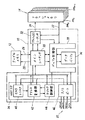
図1は、本発明の一実施例によるフラッシュメモリシステムの構成を示す。このシステムにおいて、コントローラ10、テーブルメモリ12およびフラッシュメモリ14の各チップは一枚のカードたとえばフラッシュ・ディスク・カード16上に搭載されている。カード16がホストコンピュータ18のカード・スロットに装着され、コントローラ10はホストコンピュータ18に所定規格のインタフェースたとえばPCMCIA−ATAまたはIDEインタフェース20で接続される。
【0260】
フラッシュメモリ14は、ホスト18側からコントローラ10を介してデータの書き込み/読み出しを行えるメモリであり、たとえば同一構成および機能を有する1個または複数個(n個)のAND型フラッシュEEPROMチップからなり、バス22および所要の制御線24を介してコントローラ10に接続されている。
【0270】
テーブルメモリ12は、ホスト18とは独立してコンローラ10の管理下に置かれる不揮発性の半導体メモリチップたとえばNOR型フラッシユメモリからなり、データ蓄積用のフラッシュメモリ14とは別個のバス26および制御線28を介してコントローラ10に接続されている。このテーブルメモリ12内に後述するブロック代替管理テーブルが構築される。
【0280】
図2に、本実施例におけるコントローラ10の内部の機能的構成をブロック図で示す。コントローラ10は、メインシーケンサ30、フラッシュI/Fシーケンサ32、ホストインタフェース部34、データバッファ36およびバッファ制御部38を有している。
【0290】
メインシーケンサ30は、内蔵または外付けのファームウェアにしたがって動作し、コントローラ10内の各部を制御してホスト18およびフラッシュメモリ14間のデータのやりとりを管理するだけでなく、テーブルメモリ12に対して直接アクセス可能で所要のメモリ制御を行う機能を有している。
【0300】
フラッシュI/Fシーケンサ32は、メインシーケンサ30の管理下でフラッシュメモリ14に対して直接アクセスし所要のメモリ制御を行う。
【0310】
ホストインタフェース部34は、CHSレジスタ40、アドレス変換部42、ロジック制御部44およびI/Oポート46等を含んでいる。CHSレジスタ40は、ホスト18より送られて来たCHS(シリンダ・ヘッド・セクタ)モードのアドレスを保持する。アドレス変換部42は、ホスト18からのCHSアドレスをシステム内の論理アドレスに変換するための演算機能を有するほか、論理アドレスの自動更新を行うための演算機能も有している。
【0320】
ロジック制御部44は、ホスト18側より書き込み可能または読み取り可能な各種レジスタを内蔵しており、書き込まれたコマンドを解読してアドレス変換部42やバッファ制御部38等を制御する機能を有している。
【0330】
I/Oポート46は、ホスト18のバス20に所定規格のインタフェースたとえばPCMCIA−ATAまたはIDEインタフェースで接続され、ホスト18より入力したデータおよび制御信号を各部へ転送するためのマルチプレクサ機能を有するほか、ホスト18より受信したアドレス信号をデコードするためのアドレスデコーダを内蔵している。
【0340】
データバッファ36は、揮発性の半導体メモリたとえばSRAMからなる。バッファ制御部38は、メインシーケンサ30、フラッシュI/Fシーケンサ32またはI/Oポート46からのデータバッファ36に対するデータの書き込み/読み出しの要求を受け付け、かつ調停を行って、データバッファ36のデータ書き込み/読み出し動作を制御する。
【0350】
なお、メインシーケンサ30とフラッシュI/Fシーケンサ32、ホストインタフェース部34、バッファ制御部38の各部との間はデータバスと制御線とで接続されるが、これらのデータバスはハードウェア的には共通のバスでよく、さらにはその共通バスにテーブルメモリ12を接続することも可能である。
【0360】
図3に、フラッシュメモリ14における1ブロック内の記憶領域フォーマットの一例を示す。フラッシュメモリ14の各チップFMi (i=1,2…,n)内のメモリ領域は所定数(N個)のブロックに分割され、さらに各ブロック内の記憶領域が所定のフォーマットで区分されている。
【0370】
図3のフォーマット例では、1ブロック内が512バイト(1セクタ分)のデータ格納部と、4バイトのECC(Error Check and Correction) コード格納部と、12バイトの未使用領域(Reserve )とに区分されている。1ブロックが書き込み単位の1セクタに相当するため、消去だけでなく書き込みも1ブロック単位で行われる。
【0380】
図4に、フラッシュメモリ・チップFMi の記憶領域フォーマットの一例を示す。この例では、各チップFMi 内の記憶領域が16384個のブロックに分割され、それぞれのブロックに配列順に物理アドレス0,1,…,16383が割り当てられる。
【0390】
また、本実施例では、各フラッシュメモリ・チップFMi 内でブロックの代替が行われていない場所では論理アドレスと物理アドレスとが同じ値で対応し、物理アドレスと同じ値の論理アドレスが割り当てられる。
【0400】
各フラッシュメモリ・チップFMi 内の16384個のブロックのうち、0〜15359番目のブロックは通常領域に属し、正常である限りデータ格納用ブロックとして用いられる。残りのブロックつまり15360番目から16383番目(最後)までの1024個のブロックはスペア領域に属し、通常領域内に不良のブロックが存在するときにそれに替わる代替ブロックとして用いられる。
【0410】
図4には、テーブルメモリ12内に構築されるブロック代替管理テーブルの一例も示されている。本実施例では、各フラッシュメモリ・チップFMi についてそのスペア領域のブロック数またはアドレス数と同じ個数(1024)のテーブルアドレス(物理アドレス)がブロック代替管理テーブルTBi 内に設定され、各テーブルアドレスが1対1の対応関係でいずれか1つのスペアブロックの物理アドレスに対応づけられている。
【0420】
この例では、それぞれスペア領域およびテーブル領域内で同じ配列順位を有するテーブルアドレスとスペアブロック物理アドレスとが互いに対応しており、各テーブルアドレスに一定のオフセット値AS (15360)を加算すると、そのテーブルアドレスに対応するスペアブロック物理アドレスが得られるという関係がある。
【0430】
各テーブルアドレスで指示されるテーブル記憶位置には、そのテーブルアドレスに対応するスペアブロックの状態に関する情報がブロック代替情報として所定のデータ長たとえば1ワード(16ビット)で格納される。
【0440】
図5に、本実施例におけるブロック代替情報のデータフォーマット例を示す。この1ワードのブロック代替情報B15−00 のうち、最上位2ビットB15−14 には当該(対応)スペアブロックの良否状態を示す情報がセットされる。つまり、当該スペアブロックが「正常」であるか「不良」であるかに応じてこの良否フラグビットB15−14 に「11」,「00」がセットされる。
【0450】
なお、本実施例においてブロックが「正常」であるとは、前回このスペアブロックにアクセスした際に正常であったことを意味し、必ずしも現時点の状態が正常であるとは限らない。また、「不良」と判定されたブロックには以後のアクセスを禁止するため、いったん「00」にセットされた良否フラグビットB15−14 が「11」に変わることはない。
【0460】
下位14ビットのフィールドB13−00 は、最上位ビット(良否フラグビット)B15−14 が「11」のとき有意となり、当該スペアブロックが未使用状態つまり空き状態であるのか、それとも代替ブロックとして使用中の状態であるのかを示す情報がセットされる。
【0470】
すなわち、当該スペアブロックが空き状態のときは、このフィールドB13−00 の全ビットに1がセットされる。したがって、ブロック代替情報B15−00 は全ビットが1の値つまりFFFFh になる。
【0480】
また、当該スペアブロックが代替ブロックとして使用されているときは、このフィールドB13−00 には当該スペアブロック(代替ブロック)によって代替されている通常領域内の不良ブロックに割り当てられていた論理アドレスがセットされる。
【0490】
図5には、フラッシュメモリ14の全チップFM0 ,FM1 ,…,FMn に対応するブロック代替管理テーブルTB0 ,TB1 ,…,TBn のテーブルメモリ12内の配置構造も示されている。本例では、テーブルメモリ12の物理アドレスの最下位10ビットの値がチップ1個分の各ブロック代替管理テーブルTBi の物理アドレスに相当する。そして、テーブル1個分のアドレスは[0000000000]〜[1111111111]で与えられるから、テーブルの始端位置が3C00h のときは、3FFFh が終端位置となる。
【0500】
なお、図4の例では、ブロック代替管理テーブルTBi の先頭位置(テーブルアドレス0)および2番目の位置(テーブルアドレス1)に論理アドレス4,5がそれぞれ格納(登録)されている場合を示している。
【0510】
このことは、フラッシュメモリ・チップFMi において論理アドレス4,5をそれぞれ割り当てられていた通常領域内のブロックつまり物理アドレス4,5の両ブロックが不良と判定されており、物理アドレス4の不良ブロックはテーブルアドレス0に対応するチップFMi 内の物理アドレス15360のスペアブロックで代替され、物理アドレス5の不良ブロックはテーブルアドレス1に対応するチップFMi 内の物理アドレス15361のスペアブロックで代替されていることを意味する。これらのブロック代替に伴って、論理アドレス4,5は実質的に不良ブロック(4,5)から代替ブロック(15360,15361)にそれぞれ移行している。
【0520】
フラッシュメモリ内の不良ブロックは、チップ出荷前のブロック良否検査によって検出できるのはもちろん、実際のメモリアクセス動作の中でも公知の方法で検出可能である。チップ出荷前の良否検査で検出される不良はいわゆる先天性不良であり、使用中に不良になるのはいわゆる後天性不良である。本発明では、いずれの不良ブロックも検出された順にブロック代替管理テーブルTBに登録される。その場合、図4に示すように、テーブルの先頭位置から順に1テーブルアドレスにつき1論理アドレスずつ登録されることになる。
【0530】
なお、先天性不良のブロックが各フラッシュメモリ・チップ内の所定の冗長部に記録またはリストされる場合は、そのリストの情報を基に先天性不良ブロックをブロック代替管理テーブルTBに一括登録することができる。そのようなリストが得られない場合は、システム構築時の初期化で全ブロックの良否を検査して先天性不良ブロックを割り出してもよい。あるいは、先天性不良ブロックも後天性不良ブロックと同じ扱いで実際のメモリアクセスの中で個別的に検出し、その都度ブロック代替管理テーブルTBに登録してもよい。
【0540】
図6および図7に、本実施例においてアドレス変換部42により実行されるアドレス演算の例を示す。
【0550】
本実施例では、ホスト18からのアドレスがCHSモードで与えられる。このCHSモードのアドレスには、アドレス指定の対象となる記憶場所のシリンダナンバー(C)、ヘッドナンバー(H)、セクタナンバー(S)、シリンダあたりのヘッド数(HpC)およびヘッドあたりのセクタ数(SpH)の値(データ)が含まれている。
【0560】
図6に示すように、先ずアドレス変換部42は、入力したCHSモードのアドレス情報(C,H,S,HpC,SpH)を基に次式(1)を演算して、対応する値の論理ブロックアドレス(LBA)を求める。
LBA=(C×HpC+H)SpH+S−1 ………(1)
【0570】
次に、アドレス変換部42は、上記のようにして算出した論理ブロックアドレス(LBA)とフラッシュメモリ14に含まれるチッブFMの個数(NumCHIP)とから次式(2),(3)を演算して、論理アドレスを規定するチップナンバー(CHIP− NUM)およびチップ内論理ブロックナンバー(LA− BLK)を求める。
LA− BLK=LBA/NumCHIP ………(2)
CHIP− NUM=LBA mod NumCHIP ………(3)
【0580】
なお、上式(2),(3)は一例である。フラッシュメモリ・チップFMi またはブロックの記憶領域フォーマットが変われば、上式(2),(3)とは違った演算式が用いられる。
【0590】
次に、図8〜図10につきホスト18からの読み出しのメモリアクセスに対する本システムの作用を説明する。図8および図9はコントローラ10内の処理手順を示し、図10はシステム内の各部の動作のタイミングを示す。
【0600】
本フラッシュメモリシステムに対してデータの読み出しを行うとき、ホスト18は上記したようにCHSモードのアドレス情報で読み出し位置(先頭位置)を指定してくる。また、読み出しデータの量または範囲をセクタカウント(SC)で指定し、読み出しコマンドを送ってくる。
【0610】
コントローラ10では、ホストインタフェース部34においてI/Oポート46で受信したホスト18からの読み出し指令情報(CHS,SC,コマンド)をロジック制御部44内のレジスタに格納する。以後、メインシーケンサ30が中心となって以下のような処理を実行する。
【0620】
先ず、ロジック制御部44内に設けられているホスト向けの内部ビジーフラグ(BUSY)をセットする(ステップA1 )。
【0630】
次いで、CHSレジスタ40に格納されているCHSモードの入力アドレスをアドレス変換部42において図6および図7に示すような演算によりフラッシュメモリ14内の論理アドレスに変換する(ステップA2 )。このアドレス変換で得られる論理アドレスから今回の読み出し動作の対象となるフラッシュメモリ・チップFMi が判明する。
【0640】
次に、メインシーケンサ30が、該当フラッシュメモリ・チップFMi に対応するブロック代替管理テーブルTBi を検索し、ホスト18より指定されている論理アドレスが該テーブルTBi 内に登録されているかどうかテーブル先頭位置からアドレス順に検索(サーチ)する(ステップA3 〜A9 )。
【0650】
このサーチは高速に行える。本実施例のようにテーブルメモリ12にNOR型フラッシュメモリを用いた場合、テーブル1行の検索に要する時間を100ナノ秒以下に抑えることが可能である。
【0660】
たとえば、ブロック代替管理テーブルTBi の内容が図4に示すような状態であり、アドレス変換によって得られた論理アドレスの値が2であったとする。
【0670】
この場合、ブロック代替管理テーブルTBi の検索で最初に(テーブル先頭位置より)読み出される情報は「C004」であり、照合一致しない。そこで、次に2番目のテーブル記憶位置の情報を読み出すと、「C005」であり、これも照合一致しない。次に、3番目のテーブル位置の情報を読み出すと、「FFFFh 」であり、これは対応スペアブロック(物理アドレス15361のブロック)が空き(未使用)の状態であることを示す。したがって、これ以降のテーブル記憶位置にも全て空き状態を示す「FFFFh 」が格納されていることもわかる。
【0680】
この時点で、論理アドレス2はブロック代替管理テーブルTBi に登録されていないこと、したがって目的のフラッシュメモリ読み出し位置は物理アドレス2のブロックであることが判明したので(ステップA6 )、テーブル検索を終了し(ステップA11)、この論理アドレス2をそのままアクセス先の物理アドレス2に置き換える(ステップA12)。
【0690】
そして、フラッシュI/Fシーケンサ32を通じてこの物理アドレス2で指定される該当フラッシュメモリ・チップFMi 内のブロックにアクセスし、そのアクセスしたブロックよりデータを読み出す(ステップA14)。この際、フラッシュメモリ14より読み出されたデータはバス22を介していったんデータバッファ36に格納される。
【0700】
別の例として、上記アドレス変換によって得られた論理アドレスの値が5であったとする。この場合は、上記のテーブル検索において2番目のテーブル記憶位置から「C005」が読み出され、このブロック代替情報「C005」に論理アドレス5が照合一致する(ステップA5 )。
【0710】
この時点で、論理アドレス5を割り当てられていた通常領域内の物理アドレス5のブロックが不良であること、そしてテーブルTBi の2番目の記憶位置に対応するチップ内物理アドレスの位置に該不良ブロックの替わりとなる該当の代替ブロックが配置されていることが判明する。そこで、テーブル検索を終了し(ステップA11)、照合一致のあったテーブルアドレス(1)に所定のオフセット値As (15360)を加算して、アクセス先のチップ内物理アドレス(15361)を求める(ステップA13)。
【0720】
そして、フラッシュI/Fシーケンサ32を通じてこの物理アドレス(15361)で指定される該当フラッシュメモリ・チップFMi のブロックにアクセスし、そのブロックよりデータを読み出す(ステップA14)。この場合も、フラッシュメモリ14より読み出されたデータはバス22を介してデータバッファ36に格納される。
【0730】
上記のようにしてフラッシュメモリ14より読み出されたデータにエラーがなければ、たとえばデータ読み出し終了時にフラッシュメモリ14より送られてくるステータス情報がエラーを示していなければ、正常な読み取りが行われたものと判断し(ステップA26)、直ちにデータバッファ36内の読み出しデータをホスト18側へ転送可能とする。すなわち、内部ビジーフラグ(BSY)をクリアし、ホスト18による読み出しデータの取り込みを待つ(ステップA28)。
【0740】
そして、ホスト18へのデータ転送の終了の後、今回のメモリアクセスでホスト18より与えられているセクタカウント(SC)が1のときは上記した1ブロック(1セクタ)分の読み出しでもって今回の全読み出し動作を終了する。しかし、セクタカウント(SC)が2以上のときは、最初に戻り(ステップA30)、上記と同様の手順で読み出し動作を実行する。ただし、2回目以降の論理アドレスはアドレス変換部42において自動更新(インクリメント)した値となる。
【0750】
図10の(A)には、フラッシュメモリ14より読み出された2セクタ分のデータにエラーが無い場合の各部の動作のタイミングが示されている。
【0760】
フラッシュメモリ14より読み出されたデータにエラーがある場合は、図9のステップA16〜A25の処理が行われる。このときの各部の動作のタイミングは図10の(B)に示されている。
【0770】
各フラッシュメモリ・チップFMi 内にはチップ内のメモリアレイから読み出したデータにECCエラーが発生したか否かを検出できる機能が備わっている。エラーがあったときは、データ読み出し終了時にチップFMi よりフラッシュI/Fシーケンサ32に送られてくるステータス情報でエラーが通知される。
【0780】
ECCエラーを示すステータス情報が通知されたときは、今回の読み出し対象となったブロックの記憶内容を消去する(ステップA16)。このイレース処理では、フラッシュI/Fシーケンサ32よりバス22を介して該当のフラッシュメモリ・チップFMi に消去対象のブロックを指定するアドレスや消去実行コマンド等が与えられる。そうすると、該チップFMi 内でそのブロックについてブロック消去動作が実行される。
【0790】
本実施例では、上記のように読み出し時にECCエラーを起こしたブロックについては、これを不良ブロックと認定する。この不良と認定されたブロックは、フラッシュメモリ・チップFMi において通常領域に属する通常ブロックであるときもあれば、スペア領域に属するスペアブロック(代替ブロック)のときもある。
【0800】
スペア領域内のブロックであるときは、ブロック代替管理テーブルTBi においてそのスペアブロックについての登録抹消処理を行う(ステップA18)。この登録抹消処理では、そのスペアブロックに対応するテーブル記憶位置に「0000h 」を書き込み、そのスペアブロックが「不良」であること、したがって代替ブロックでも代替可能ブロックでもないことを明示し、以後のアクセスを禁止する。こうして、「不良」と判定したスペアブロックをブロック代替管理テーブルTBi から登録抹消する。
【0810】
今回不良と認定されたブロックが通常領域内のブロックであるときは、上記のようなブロック代替管理テーブルTBi における登録抹消処理(ステップA18)は不要であり、この処理をスキップして(ステップA19)、空きブロックサーチ(ステップA20)を行う。
【0820】
この空きブロックサーチでは、今回不良と認定されたブロックに換わるべき空き状態のスペアブロックを捜す。具体的には、ブロック代替管理テーブルTBi においてテーブル先頭位置から順にテーブル記憶位置にアクセスし、空き情報「FFFFh 」が格納されている最先(先頭)の位置を捜し出す。そして、その捜し出したテーブル位置を基に、上記したようなテーブルアドレスとスペアブロック物理アドレスとの対応関係から、スペア領域内で未だ空き状態になっているスペアブロックの中の先頭ブロックを割り出す。
【0830】
本実施例では、上記のようなブロック代替管理テーブルTBi におけるスペアブロック登録抹消および空きブロックサーチの各処理(ステップA18,A20)をフラッシュメモリ14における不良ブロックのイレース処理(ステップA16)と並行して実行することが可能である。
【0840】
すなわち、ブロック代替管理テーブルTBi が位置するテーブルメモリ12と不良ブロックが位置するフラッシュメモリ14とは別々のバス26,22に接続されているので、コントローラ10は両メモリ12,14に対して並列的にアクセスし、両メモリ12,14に所要のメモリ動作を並列的または同時的に行わせることができる。
【0850】
上記のようにして新規の代替ブロックとなるべき空きのスペアブロックを割り出したなら、次に、このスペアブロックをイレース(初期化)したうえで、データバッファ36に格納されているデータ(フラッシュメモリ14より今回読み出されたデータ)を該スペアブロックに書き込む(ステップA21)。
【0860】
このデータ書き込み処理は、今回不良と認定されたブロックにいままで蓄積されていたデータを新規代替ブロックとなるべきスペアブロックに移し替える処理にほかならない。
【0870】
この初期化のイレース処理は上記不良ブロックに対するイレース処理(ステップA16)と同様にして行われる。また、該スペアブロックへのデータの書き込みに際しては、フラッシュI/Fシーケンサ32からは該スペアブロックを指定するアドレスと書き込みを指示する所要のコマンドとが、データバッファ36からは書き込み対象のデータが、それぞれ所定のタイミングで該当のフラッシュメモリ・チップFMi に送り込まれる。そうすると、そのフラッシュメモリ・チップFMi 内では、書き込みコマンドが実行され、該当スペアブロックに該データが書き込まれる。
【0880】
このスペアブロックにおける初期化およびデータ書き込みは、首尾良く行われたかそれとも失敗したのか、上記と同様にフラッシュメモリ・チップFMi からのステータス情報を基に確認をとる(ステップA12)。失敗したときは、当該スペアブロックを「不良」と認定し、新規の代替ブロックとして使える正常なスペアブロックが得られるまで、スペアブロックに関する上記一連の処理(A18,A20,A21)を繰り返す(ステップA23)。その際、ブロック代替管理テーブルTBi においては、テーブルアドレスの上位位置から順に「0000h 」の書き込み(登録抹消)が行われる。
【0890】
そして、新規の代替ブロックとして使えた正常なスペアブロックが決まったならば、次にそのスペアブロックに対応するブロック代替管理テーブルTBi のテーブル記憶位置に今回のメモリアクセスに係る論理アドレス(ステップA2 )の値を格納(登録)する(ステップA24)。これで、この論理アドレスはこの新規代替ブロックに割り付けられたことになる。
【0900】
次に、今回の読み出しデータエラーが訂正不能であった場合は、この時点でロジック制御部44内のエラービットフラグをセットする(ステップA25)。次いで、ビジーフラグ(BSY)をクリアして(ステップA27)、データバッファ36内の読み出しデータをホスト18へ転送可能とする(ステップA28)。
【0910】
次に、図11〜図15につきホスト18からの書き込みのメモリアクセスに対する本システムの作用を説明する。図11〜図13はコントローラ10内の処理手順を示し、図14〜図15はシステム内の各部の動作のタイミングを示す。
【0920】
データの書き込みを行うとき、ホスト18はCHSモードのアドレス情報で書き込み位置(先頭位置)を指定し、セクタカウント(SC)で書き込みデータの量または長さを指定し、書き込みコマンドで指示してくる。
【0930】
コントローラ10では、ホストインタフェース部34においてI/Oポート46で受信したホスト18からの書き込み指令情報(CHS,SC,コマンド)をロジック制御部44内のレジスタに格納する。以後、メインシーケンサ30が中心となって以下のような処理を実行する。
【0940】
先ず、ロジック制御部44内の内部ビジーフラグ(BUSY)をセットする(ステップB1 )。
【0950】
次いで、アドレス変換部42においてCHSモードのアドレスからフラッシュメモリ内論理アドレスへのアドレス変換(演算)が行われる(ステップB2 )。
【0960】
次に、メインシーケンサ30が、上記した読み出し動作のときと同様に、該当フラッシュメモリ・チップFMi に対応するブロック代替管理テーブルTBi を検索し、ホスト18より指定されている論理アドレスがテーブルTBi 内に登録されているかどうかテーブル先頭位置からアドレス順に検索し(ステップB3 〜B9 )、検索結果にしたがって該論理アドレスに対応するブロックの物理アドレスを割り出す。
【0970】
すなわち、該論理アドレスがテーブルTBi 内に登録されているときは、その登録位置のテーブルアドレスに対応する代替ブロックの物理アドレスが割り出される(ステップB13)。また、該論理アドレスがテーブルTBi 内に登録されていないときは、その論理アドレスと同じ値の物理アドレスが割り出される(ステップB12)。
【0980】
次に、その割り出された物理アドレスで指示される当該フラッシュメモリ・チップFMi 内のブロックをイレース(初期化)する。この初期化のイレース処理は、上記した読み出し動作における不良ブロックのイレース(ステップA16)と同様の手順で行われる。
【0990】
そして、ホスト18からの書き込みデータの転送に応ずるため内部ビジーフラグ(BSY)をクリアしておいて(ステップB15)、イレース処理(ステップB14)が首尾良く完了したことを当該フラッシュメモリ・チップFMi からのステータス情報で確認する(ステップB16,B17)。さらに、ホスト18からのデータが全てデータバッファ36にロードされたことも確認する(ステップB28)。
【1000】
そして、内部ビジーフラグ(BSY)をセットしたうえで(ステップB29)、フラッシュメモリ14へのデータ書き込みを行う(ステップB30)。このデータ書き込み処理は、上記した読み出し動作におけるデータエラー発生時のデータ移し替えのための書き込み処理(ステップA21)と同様の手順で行われる。
【1010】
すなわち、フラッシュI/Fシーケンサ32からは該当の物理アドレスと書き込みコマンドとが、データバッファ36からはホスト18より送られて来た書き込み対象のデータが、それぞれ所定のタイミングで該当のフラッシュメモリ・チップFMi に送り込まれる。フラッシュメモリ・チップFMi 内では、書き込みコマンドが実行され、該当ブロックに該データが書き込まれる。
【1020】
そして、この書き込みが首尾良く行われたことを当該フラッシュメモリ・チップFMi からのステータス情報で確認する(ステップB31)。ホスト18より与えられているセクタカウント(SC)が1のときはこれで全処理を終了し、セクタカウント(SC)が2以上のときは最初に戻り(ステップB42)、上記と同様の手順で読み出し動作を実行する。ただし、2回目以降の論理アドレスはアドレス変換部42において1つインクリメントした値となる。
【1030】
図14の(A)には、何のエラーや障害も発生することなくホストからの2セクタ分のデータがフラッシュメモリ14に書き込まれた場合の各部の動作のタイミングが示されている。
【1040】
上記した該当ブロックに対するイレース処理(ステップB14)が失敗したときは、図12のステップB20〜B26の処理が行われる。このときの各部の動作のタイミングは図14の(B)に示されている。
【1050】
このイレース処理(ステップB14)でエラーがあったときは、イレース動作終了後に当該フラッシュメモリ・チップFMi よりフラッシュI/Fシーケンサ32に送られてくるステータス情報でエラーが通知される。
【1060】
本実施例では、イレース・エラーが発生したブロックについては、これを不良ブロックと認定する。この不良と認定されたブロックは、フラッシュメモリ・チップFMi において通常領域に属する通常ブロックであるときもあれば、スペア領域に属するスペアブロック(代替ブロック)のときもある。
【1070】
スペア領域内のブロックであるときは、ブロック代替管理テーブルTBi においてそのスペアブロックについての登録抹消処理を行う(ステップB19)。この登録抹消処理は、上記した読み出し動作における登録抹消処理(ステップA18)と同様の手順で行われる。
【1080】
今回不良と認定されたブロックが通常領域内のブロックであるときは、上記した読み出し動作のときと同様に、テーブル内登録抹消処理(ステップB19)をスキップして(ステップB20)、空きブロックサーチ(ステップB21)を行う。
【1090】
この空きブロックサーチの処理も、上記した読み出し動作における空きブロックサーチ(ステップA20)と同様の手順で行われ、空き状態のスペアブロックの中で最も上位位置にあるブロックを割り出す。
【1100】
上記のようにして新規の代替ブロックとなるべき空きのスペアブロックを割り出したなら、次に、このスペアブロックに対し上記と同様の手順で初期化のイレースを行う(ステップB22)。
【1110】
このイレースが首尾良く行われたならそのスペアブロックを新規代替ブロックとして使える正常なブロックと認定し、イレースが失敗したならこのスペアブロックを不良ブロックと認定し、正常なスペアブロックが見つかるまで上記の処理を繰り返す(ステップB24)。この点は、上記した読み出し動作において新規代替ブロックを決定するときの処理(ステップA18〜A23)と類似している。
【1120】
そして、正常にイレースされたスペアブロックに突き当たったときは、このスペアブロックを代替ブロックとして登録するため、ブロック代替管理テーブルTBi においてそのスペアブロックの物理アドレスに対応するテーブルアドレスのテーブル位置に今回のメモリアクセスで指定された論理アドレス(ステップB2 )を格納しておく(ステップB25)。
【1130】
また、今回のデータ書き込みのアクセス先をこの登録された代替ブロックに変更しておく(ステップB26)。
【1140】
上記フラッシュメモリ14へのデータ書き込み処理(ステップB30)が失敗したときは、図13のステップB32〜B38の処理が行われる。このときの各部の動作のタイミングは図15に示されている。
【1150】
このデータ書き込み処理(ステップB30)でエラーがあったときも、当該フラッシュメモリ・チップFMi より書き込み動作終了後に送られてくるステータス情報でエラーが通知される。
【1160】
本実施例では、データ書き込みの失敗したブロックについても、これを不良ブロックと認定する。そして、この不良ブロックに替わるべき代替用のスペアブロックを決定し、そのスペアブロックにアクセスして今回のホスト18からのデータを書き込む。この一連の代替処理(ステップB32〜B38)は、上記した読み出し動作におけるデータエラー発生時の代替処理(ステップA17〜A24)と同様の手順で行われる。
【1170】
その結果、上記のような所定の条件を満たす新規の代替用スペアブロックに今回のメモリアクセスでホスト18より送られてきたデータが書き込まれる。そして、このスペアブロックに対応するブロック代替管理テーブルTBi のテーブル記憶位置に今回ホスト18より指定された論理アドレスの値が格納(登録)されることで(ステップB38)、次回にこの論理アドレスが指定されたときはこの新規代替ブロックがアクセス先となる。
【1180】
なお、図8、図9、図11〜図13のフローチャートに示す読み出し動作および書き込み動作の手順は、説明の便宜上、図3に示すような1ブロック=1セクタのフォーマットに対応させている。1ブロックに複数のセクタが含まれている場合は、1セクタの転送毎に最初から処理を繰り返すことはせず、1ブロック分の全データをデータバッファ36に格納し、ホストインタフェース部34とホスト18との間だけで1セクタ単位のデータ転送を繰り返す。
【1190】
上記したように、本実施例のフラッシュメモリシステムでは、フラッシュメモリ14の外部で、かつ別個のバス26上に好ましくはNOR型フラッシュメモリからなる不揮発性のテーブルメモリ12を設け、このテーブルメモリ12内に上記したようなブロック代替管理テーブルTBを構築する。
【1200】
ホスト18からのメモリアクセス要求を受ける度に、コントローラ10(より詳細にはメインシーケンサ30)が該テーブルTBを検索すると、テーブルの内容とホストより指定された論理アドレスとの照合によりブロック代替の要否判断が自動的に行われ、アクセス先となる該当ブロックが短時間で判明する。このアクセス先のブロックは、少なくとも前回アクセスされた時点では正常な記憶領域を有していたものであり、今回も正常であることの蓋然性は高い。
【1210】
本実施例によれば、最初から不良と分かっているブロックにアクセスするようなことを回避することができる。これにより、不良のアレイ領域へのアクセスに起因してフラッシュメモリが受ける有害なストレスを可及的に少なくすることができる。
【1220】
そして、仮にアクセス先のブロックが不良になっていた場合は、ブロック代替管理テーブルTBを参照しつつ、その不良ブロックに替わるべき代替ブロックを適確かつ迅速に決定し、同時にそのような新規のブロック代替に追随してテーブルTBの内容も適宜更新(書き換え)するようにしている。
【1230】
上記したように、本フラッュメモリシステムでは、ブロック代替管理テーブルTB上でブロック代替情報を一元管理しているため、効率の高いブロック代替管理を実現できる。特に、テーブルTB内には不良と判定された通常ブロックに係わる論理アドレスのみ登録すればよく、代替ブロックを指示するための特別なポインタを登録する必要もない。したがって、テーブル容量は少なくて済み、フラッシュメモリの大容量化に十分対応できる。
【1240】
また、ブロック代替管理テーブルTBには電源の入/切に関係なくブロック代替情報が保持されるため、電源投入直後等で行われるシステム初期化の中でテーブル形成のための処理も時間も一切不要である。
【1250】
また、本実施例では、ブロック代替管理テーブルTBを与えるテーブルメモリ12とデータ格納用のメモリ空間を与えるフラッシュメモリ14とが別々のバス26,22に接続されているので、ブロック代替管理テーブルTBi 内の処理(検索・更新等)をフラッシュメモリ14側の動作と独立させて実行することが可能であり、ブロック代替管理を効率よく展開できる。
【1260】
もっとも、上記した実施例は一例であり、本発明におけるブロック代替管理方式とりわけブロック代替管理テーブルTBに関連する諸機能は種々の応用および変形が可能である。
【1270】
たとえば、上記した実施例では、ホスト18からのメモリアクセス要求を受けると、コントローラ10(メインシーケンサ30)は即座に(無条件)でブロック代替管理テーブルTBi を検索するようにした。しかし、先ずはホストから指定された論理アドレスのブロックにそのままアクセスし、そのブロックが不良であることが冗長部のブロック関連情報等から確認された時点で、ブロック代替管理テーブルTBを参照する方法も可能である。この場合でも、ブロック代替管理テーブルTBを通して該当の代替ブロックへアクセスすることができる。
【1280】
また、ブロック代替管理テーブルTBの更新は常に論理アドレス、不良フラグ等のデータ書き込みの形態で行われる。テーブルの初期化で全テーブル位置に書き込まれる空き情報(FFFFh )を除き、いったん書き込まれたデータが消去されることはない。その意味で、上記実施例のようにブロック代替管理テーブルTBに用いる不揮発性のメモリとして、AND型フラシュメモリは機能的にもコスト的にも有利である。
【1290】
しかし、EEPROMやFRAMのような他の種類の不揮発性メモリも使用可能である。なお、テーブルメモリ12に用いた不揮発性半導体メモリに他の用途のテーブルや各種設定値、ファームウェア等も一緒に格納できることはもちろんである。
【1300】
あるいは、個々のフラッシュメモリ・チップFMi 内の冗長領域にブロック代替管理テーブルTBi を設けることも可能である。その場合、テーブル内の処理とチップ内の本来のメモリ動作とは競合することになるため、特別の時分割制御が必要となる。
【1310】
上記実施例では、ブロック代替管理テーブルTBにおいて、フラッシュメモリ・チップ内スペア領域のブロック数またはアドレス数と同じ個数のテーブルアドレス(物理アドレス)が設定され、各テーブルアドレスが1対1の対応関係でいずれか1つのスペアブロックの物理アドレスに対応づけられていた。そして、それぞれスペア領域およびテーブル領域内で同じ配列順位を有するテーブルアドレスとスペアブロック物理アドレスとが互いに対応しており、各テーブルアドレスに一定のオフセット値AS を加算すると、そのテーブルアドレスに対応するスペアブロック物理アドレスが得られるという関係があった。
【1320】
しかし、スペア領域のブロック数またはアドレス数とテーブルアドレスとは必ずしも同数である必要はない。オフセットAs は任意に設定可能であり、一定値でなくてもよい。重要なのは両者の間に1対1の対応関係があり、その対応関係が管理されるということである。
【1330】
また、ブロック代替管理テーブル内の検索方向または検索順次も任意に取り決めることが可能である。
【1340】
上記実施例におけるフラッシュ・ディスク・システムの構成、特にコントローラ内部の構成またはレイアウトは一例であり、種々の変形が可能である。上記した実施例においてホストより与えられるアドレスの形態(CHSモード)も一例であり、ホストが最初からフラッシュメモリ内の論理アドレスを与えてきてもよく、他のモードのアドレスを与えてきてもよい。種々多様な構成または機能を有するホストないしホストインタフェースが使用可能である。
【1350】
【発明の効果】
以上説明したように、本発明のフラッシュメモリシステムによれば、少ない資源で効率よく信頼性の高いブロック代替管理を行うことができる。
【図面の簡単な説明】
【図1】本発明の一実施例によるフラッシュメモリシステムの構成を示すブロック図である。
【図2】実施例におけるコントローラの内部の機能的構成を示すブロック図である。
【図3】実施例のフラッシュメモリにおけるブロック内記憶領域フォーマットの一例を示す図である。
【図4】実施例におけるフラッシュメモリチップ内記憶領域フォーマットの一例とブロック代替管理テーブルの構成例を示す図である。
【図5】実施例におけるブロック代替情報のデータフォーマット例を示す図である。
【図6】実施例のアドレス演算部で実行されるアドレス演算の例を示す図である。
【図7】実施例のアドレス演算部で実行されるアドレス演算の例を示す図である。
【図8】実施例における読み出し動作の処理手順を示すフローチャートである。
【図9】実施例における読み出し動作の処理手順を示すフローチャートである。
【図10】実施例の読み出し動作における各部の動作のタイミングを示す図である。
【図11】実施例における書き込み動作の処理手順を示すフローチャートである。
【図12】実施例における書き込み動作の処理手順を示すフローチャートである。
【図13】実施例における書き込み動作の処理手順を示すフローチャートである。
【図14】実施例の書き込み動作における各部の動作のタイミングを示す図である。
【図15】実施例の書き込み動作における各部の動作のタイミングを示す図である。
【符号の説明】
10 コントローラ
12 テーブルメモリ
14 フラッシュメモリ
18 ホストコンピュータ
22,26 バス
30 メインシーケンサ
32 フラッシュI/Fシーケンサ
34 ホストインタフェース部
36 データバッファ
38 バッファ制御部
42 アドレス変換部[0010]
TECHNICAL FIELD OF THE INVENTION
The present invention relates to a memory system including a flash memory.
[0020]
[Prior art]
2. Description of the Related Art In recent years, a flash EEPROM (hereinafter referred to as a flash memory) has attracted attention as a semiconductor memory replacing a magnetic memory such as a hard disk or a floppy disk. A flash memory is an electrically rewritable nonvolatile semiconductor memory with low power consumption, and is widely used for portable devices and the like because of its light weight, small size, and good earthquake resistance.
[0030]
In a flash memory, an EEPROM cell array in a chip is divided into a plurality of blocks, and each block is further divided into one or a plurality of sectors. Usually, programming (writing) and reading are performed in sector units, and erasing is performed in block units.
[0040]
Generally, in a computer system using a flash memory as an external storage device, a controller dedicated to the flash memory is used. The host computer (for example, a personal computer) may instruct this controller to write or read data. The controller directly controls writing and reading of data to and from the flash memory in response to an instruction from the host, and also performs memory management such as data rewriting and batch erasing for each block.
[0050]
As a part of such memory management, the controller is required to have a management function of recognizing a defective (defective) block in which data cannot be written or read normally and replacing each defective block with another normal block.
[0060]
A general flash memory system prepares an appropriate number of spare or spare blocks in a part of the memory area so that the existence or occurrence of such a defective block is allowed to a certain number. Usually, these spare blocks are used as replacement blocks.
[0070]
In a conventional flash memory system, a flag or status information indicating whether the block is normal or bad is stored in a redundant portion of each block of the flash memory. Also, address information (pointer) indicating the storage position of the replacement block to be replaced is stored. Each time a memory access is performed by the host, the controller reads the block pass / fail flag information of the addressed block, and if the block is “normal”, accesses the block as it is, and if “bad”, indicates with the pointer. To access another block (alternate block).
[0080]
[Problems to be solved by the invention]
As described above, in the conventional method, the block related information such as the block pass / fail flag is stored (saved) in the redundant portion of each block in the flash memory, and the controller stores the block related information of the block every time the memory is accessed. By reading, it is determined whether or not block replacement is necessary.
[0090]
Therefore, when the address from the host side designates a bad block, the bad block is accessed, the block related information is read therefrom, the necessity of block replacement is determined, and then the replacement block is accessed. . That is, a data read operation for two blocks is performed.
[0100]
Such a block replacement management method is not only inefficient, but also necessitates determining whether block replacement is necessary based on unreliable data (block-related information) read from a bad block. There is a problem that the reliability of the block replacement function is low. Furthermore, access to a bad block may give harmful stress to the flash memory, and may accelerate the deterioration of the memory.
[0110]
During initialization immediately after power-on or immediately after reset release, the controller reads the redundant parts of all the blocks in the flash memory, collects the respective block-related information, and based on the collected block-related information. For example, a method of forming a table for block replacement on a volatile memory such as an SRAM has been considered.
[0120]
According to this method, in response to a memory access from the host, a block replacement table is first referred to determine whether the addressed block is normal or defective, that is, whether or not block replacement is necessary. Is determined, and the block or the substitute block is accessed.
[0130]
However, even with this method, a defective block is accessed at the time of initialization (table formation), and the number of accesses is reduced, but the above problem is not basically solved. In addition, since this method collects block-related information for all blocks in the flash memory, there is a problem that the processing time required for forming the block replacement table is long and the storage capacity required for the table memory is large. In recent years, flash memories have been rapidly increasing in capacity, and this disadvantage has become more pronounced.
[0140]
The present invention has been made in view of the above problems, and has as its object to provide a flash memory system capable of efficiently performing block replacement management with a small amount of resources.
[0150]
It is another object of the present invention to provide a flash memory system which can perform unnecessary block access management with high reliability and efficiency by eliminating useless access to a bad block.
[0160]
A further object of the present invention is to provide a flash memory system that can efficiently access a substitute block that replaces a defective block in a short time.
[0170]
[Means for Solving the Problems]
In order to achieve the above object, a first flash memory system according to the present invention includes a flash memory configured to divide a storage area into a plurality of blocks, and to erase storage data collectively in block units; The address assigned to the block determined to be bad in the memorySearchableBlock replacement information registration for registering and providing a replacement address indicating a storage position of a replacement block to be used in place of the defective blockmemoryAnd an address given for memory access to the flash memory, and the input address is the block replacement information registrationmemoryIf the block is not registered in the flash memory, the block in the flash memory specified by the input address is accessed, and the input address is registered in the block replacement information.memoryAccess to a block in the flash memory designated by the alternative address corresponding to the input addressMemory control unitAndThe memory control unit is connected to the flash memory via a first bus, the memory control unit is connected to the block replacement information registration memory via a second bus, and the memory control unit via the first bus. The operation between the flash memory and the flash memory and the operation between the memory control unit and the block replacement information registration memory via the second bus are performed independently.
[0180]
The second flash memory system according to the present invention may further comprise a flash memory configured to divide a storage area into a plurality of blocks and collectively erase storage data in block units, and determine that the flash memory is defective. The logical address assigned to the blockSearchableBlock replacement information registration that registers and assigns, as a replacement address, a physical address assigned to a replacement block to be used in place of each defective block.memoryInputting an address given for memory access to the flash memory, converting the input address into a logical address in the flash memory, and registering the logical address with the block replacement informationmemoryWhen the logical address is not registered in the flash memory, the block in the flash memory indicated by the logical address is accessed, and the logical address is registered in the block replacement information.memoryAccess to the block in the flash memory designated by the substitute address corresponding to the logical addressMemory control unitAndThe memory control unit is connected to the flash memory via a first bus, the memory control unit is connected to the block replacement information registration memory via a second bus, and the memory control unit via the first bus. The operation between the flash memory and the flash memory and the operation between the memory control unit and the block replacement information registration memory via the second bus are performed independently.
[0190]
According to the present invention, the memory control unit and the block replacement information registration memory are independent of the data read / write / erase operations performed between the memory control unit and the flash memory via the first bus. Operations such as search / update are performed via the second bus. In one aspect, if the block accessed by the memory control unit in the flash memory is found to be a defective block, the memory control unit places the first and second buses in the flash memory and the block replacement information registration memory, respectively. In parallel, an erasing process for erasing the storage contents of the defective block in the flash memory and a process of searching for and updating the registration information in the block replacement information registration memory are performed in parallel. By such parallel processing, block replacement management can be efficiently developed.
[0200]
In the present invention, the block replacement information registration memory has a plurality of storage locations corresponding one-to-one with a plurality of spare blocks set as replacement blocks in the flash memory, and one of the spare blocks is replaced. When used as a block, it may include a non-volatile storage means for storing address information indicating an address assigned to a defective block replaced by the defective block in a storage location corresponding to the spare block.
[0210]
Further, at each storage location in the block replacement information registration memory, when the corresponding spare block is not used as a replacement block, first status information indicating its empty state may be stored. Second status information indicating whether the spare block to be used is normal or defective may also be stored.
[0220]
The block replacement information registration memory includes address generation means for obtaining an address of a replacement block replacing each defective block based on an address of a storage location where address information corresponding to the defective block is stored. Good. In this case, preferably, the address generation means obtains the address of the replacement block replacing the bad block by adding a predetermined offset value to the address of the storage location where the address information corresponding to the bad block is stored. Good.
[0230]
In the present invention, preferably, the nonvolatile storage means may be a NOR flash memory.
[0240]
BEST MODE FOR CARRYING OUT THE INVENTION
Hereinafter, embodiments of the present invention will be described with reference to the accompanying drawings.
[0250]
FIG. 1 shows a configuration of a flash memory system according to an embodiment of the present invention. In this system, each chip of the
[0260]
The
[0270]
The
[0280]
FIG. 2 is a block diagram showing a functional configuration inside the
[0290]
The
[0300]
The flash I /
[0310]
The
[0320]
The
[0330]
The I /
[0340]
The
[0350]
The
[0360]
FIG. 3 shows an example of a storage area format in one block in the
[0370]
In the format example of FIG. 3, one block has a 512-byte (one sector) data storage unit, a 4-byte ECC (Error Check and Correction) code storage unit, and a 12-byte unused area (Reserve). It is classified. Since one block corresponds to one sector of a writing unit, not only erasing but also writing is performed in units of one block.
[0380]
FIG. 4 shows an example of a storage area format of the flash memory chip FMi. In this example, the storage area in each chip FMi is divided into 16384 blocks, and the
[0390]
In the present embodiment, the logical address and the physical address correspond to the same value in a place where the replacement of the block is not performed in each flash memory chip FMi, and the logical address having the same value as the physical address is assigned.
[0400]
Of the 16384 blocks in each flash memory chip FMi, the 0th to 15359th blocks belong to a normal area and are used as data storage blocks as long as they are normal. The remaining blocks, that is, the 1024 blocks from the 15360th to the 16383th (last) belong to the spare area, and are used as replacement blocks when a defective block exists in the normal area.
[0410]
FIG. 4 also shows an example of a block replacement management table constructed in the
[0420]
In this example, the table address and the spare block physical address having the same arrangement order in the spare area and the table area respectively correspond to each other, and when a certain offset value AS (15360) is added to each table address, the table address becomes There is a relationship that a spare block physical address corresponding to the address is obtained.
[0430]
At the table storage location designated by each table address, information on the state of the spare block corresponding to the table address is stored as block replacement information with a predetermined data length, for example, 1 word (16 bits).
[0440]
FIG. 5 shows an example of the data format of the block replacement information in the present embodiment. In the one-word block replacement information B15-00, information indicating the pass / fail state of the (corresponding) spare block is set in the most significant two bits B15-14. That is, "11" and "00" are set in the pass / fail flag bits B15-14 according to whether the spare block is "normal" or "bad".
[0450]
It should be noted that in the present embodiment, that the block is “normal” means that it was normal when the spare block was accessed last time, and the current state is not always normal. Further, since the subsequent access to the block determined to be "bad" is prohibited, the pass / fail flag bit B15-14 once set to "00" does not change to "11".
[0460]
The field B13-00 of the lower 14 bits becomes significant when the most significant bit (pass / fail flag bit) B15-14 is "11", and indicates whether the spare block is in an unused state, that is, an empty state, or is being used as a substitute block. The information indicating whether the state is the state of is set.
[0470]
That is, when the spare block is empty, 1 is set to all bits of the field B13-00. Therefore, all the bits of the block replacement information B15-00 have a value of 1, that is, FFFFh.
[0480]
When the spare block is used as a replacement block, the field B13-00 contains the logical address assigned to the defective block in the normal area replaced by the spare block (replacement block). Is done.
[0490]
FIG. 5 also shows an arrangement structure in the
[0500]
Note that the example of FIG. 4 shows a case where the
[0510]
This means that in the flash memory chip FMi, the blocks in the normal area to which the
[0520]
Defective blocks in the flash memory can be detected not only by block quality inspection before chip shipment but also by a known method in actual memory access operation. The defect detected by the pass / fail inspection before the chip is shipped is a so-called congenital defect, and the defect during use is a so-called acquired defect. In the present invention, all the bad blocks are registered in the block replacement management table TB in the order of detection. In this case, as shown in FIG. 4, one logical address is registered for each table address in order from the top position of the table.
[0530]
When a birth defect block is recorded or listed in a predetermined redundant portion in each flash memory chip, the birth defect block is collectively registered in the block replacement management table TB based on the information in the list. Can be. If such a list cannot be obtained, the integrity of all blocks may be checked by initialization at the time of system construction to determine congenital bad blocks. Alternatively, the congenital bad block may be individually detected in actual memory access in the same manner as the acquired bad block, and registered in the block replacement management table TB each time.
[0540]
FIG. 6 and FIG. 7 show examples of the address calculation executed by the
[0550]
In this embodiment, the address from the
[0560]
As shown in FIG. 6, first, the
LBA = (C × HpC + H) SpH + S−1 (1)
[0570]
Next, the
LA− BLK = LBA / NumCHIP (2)
CHIP− NUM = LBA mod NumCHIP (3)
[0580]
The above equations (2) and (3) are examples. If the storage area format of the flash memory chip FMi or the block changes, an arithmetic expression different from the above expressions (2) and (3) is used.
[0590]
Next, the operation of the present system with respect to the memory access for reading from the
[0600]
When data is read from the flash memory system, the
[0610]
In the
[0620]
First, an internal busy flag (BUSY) for the host provided in the
[0630]
Next, the input address in the CHS mode stored in the
[0640]
Next, the
[0650]
This search can be performed at high speed. When a NOR flash memory is used as the
[0660]
For example, it is assumed that the contents of the block replacement management table TBi are in a state as shown in FIG. 4, and the value of the logical address obtained by the address conversion is 2.
[0670]
In this case, the information read first (from the table top position) in the search of the block replacement management table TBi is “C004”, and the information does not match. Then, when the information of the second table storage position is read next, it is "C005", and this also does not match. Next, when the information of the third table position is read, it is "FFFFh", which indicates that the corresponding spare block (the block of the physical address 15361) is empty (unused). Therefore, it can be seen that "FFFFh" indicating the empty state is also stored in all the table storage positions thereafter.
[0680]
At this point, it has been found that the
[0690]
Then, a block in the flash memory chip FMi specified by the
[0700]
As another example, assume that the value of the logical address obtained by the address conversion is 5. In this case, "C005" is read from the second table storage position in the above table search, and the
[0710]
At this point, the block of the
[0720]
Then, a block of the flash memory chip FMi specified by the physical address (15361) is accessed through the flash I /
[0730]
If there is no error in the data read from the
[0740]
Then, after the data transfer to the
[0750]
FIG. 10A shows the operation timing of each unit when there is no error in the data of two sectors read from the
[0760]
If there is an error in the data read from the
[0770]
Each flash memory chip FMi has a function of detecting whether an ECC error has occurred in data read from a memory array in the chip. If there is an error, the error is notified by the status information sent from the chip FMi to the flash I /
[0780]
When the status information indicating the ECC error is notified, the storage contents of the block to be read this time are erased (step A16). In this erasing process, an address for specifying a block to be erased, an erase execution command, and the like are given from the flash I /
[0790]
In this embodiment, a block in which an ECC error has occurred at the time of reading as described above is identified as a defective block. The block determined to be defective may be a normal block belonging to the normal area in the flash memory chip FMi, or may be a spare block (substitute block) belonging to the spare area.
[0800]
If the block is in the spare area, the block replacement management table TBi performs a registration deletion process on the spare block (step A18). In this registration deletion processing, “0000h” is written in the table storage location corresponding to the spare block, and it is clearly indicated that the spare block is “bad”, that is, it is neither a substitute block nor a replaceable block. Ban. Thus, the registration of the spare block determined to be "bad" is deleted from the block replacement management table TBi.
[0810]
If the block determined to be defective this time is a block in the normal area, the deregistration processing (step A18) in the block replacement management table TBi as described above is unnecessary, and this processing is skipped (step A19). , An empty block search (step A20).
[0820]
In this empty block search, an empty spare block to be replaced with a block determined to be defective this time is searched for. More specifically, in the block replacement management table TBi, the table storage positions are sequentially accessed from the table head position, and the earliest (head) position where the empty information “FFFFh” is stored is searched for. Then, based on the found table position, the head block among the spare blocks that are still empty in the spare area is determined from the correspondence between the table address and the spare block physical address as described above.
[0830]
In the present embodiment, the respective processes (steps A18 and A20) of the spare block registration deletion and the empty block search in the block replacement management table TBi as described above are performed in parallel with the defective block erasing process (step A16) in the
[0840]
That is, since the
[0850]
When an empty spare block to be a new substitute block is determined as described above, the spare block is erased (initialized), and then the data (flash memory 14) stored in the
[0860]
This data writing process is nothing but a process of transferring data that has been accumulated in a block that has been determined to be defective this time to a spare block that is to be a new replacement block.
[0870]
This initialization erasing process is performed in the same manner as the erasing process for the defective block (step A16). When writing data to the spare block, the flash I /
[0880]
Whether the initialization and data writing in the spare block have been successfully performed or failed is confirmed based on the status information from the flash memory chip FMi in the same manner as described above (step A12). If the spare block has failed, the spare block is determined to be "bad" and the above series of processing (A18, A20, A21) for the spare block is repeated until a normal spare block usable as a new substitute block is obtained (step A23). ). At this time, in the block replacement management table TBi, “0000h” is written (deregistered) in order from the upper position of the table address.
[0890]
When a normal spare block that can be used as a new spare block is determined, the logical address (step A2) related to the current memory access is stored in the table storage position of the block replacement management table TBi corresponding to the spare block. The value is stored (registered) (step A24). This means that the logical address has been assigned to the new substitute block.
[0900]
Next, if the current read data error cannot be corrected, an error bit flag in the
[0910]
Next, the operation of the present system with respect to the memory access for writing from the
[0920]
When writing data, the
[0930]
The
[0940]
First, an internal busy flag (BUSY) in the
[0950]
Next, the
[0960]
Next, the
[0970]
That is, when the logical address is registered in the table TBi, the physical address of the substitute block corresponding to the table address of the registered position is determined (step B13). If the logical address is not registered in the table TBi, a physical address having the same value as the logical address is determined (step B12).
[0980]
Next, the block in the flash memory chip FMi indicated by the determined physical address is erased (initialized). This initialization erasing process is performed in the same procedure as that for erasing a defective block in the above-described read operation (step A16).
[0990]
Then, the internal busy flag (BSY) is cleared to respond to the transfer of the write data from the host 18 (step B15), and the fact that the erase processing (step B14) has been successfully completed is notified from the flash memory chip FMi. Confirm with the status information (steps B16 and B17). Further, it is also confirmed that all the data from the
[1000]
Then, after setting the internal busy flag (BSY) (step B29), data writing to the
[1010]
That is, the relevant physical address and the write command are sent from the flash I /
[1020]
Then, it is confirmed by the status information from the flash memory chip FMi that the writing has been successfully performed (step B31). When the sector count (SC) given by the
[1030]
FIG. 14A shows the operation timing of each unit when data of two sectors from the host is written to the
[1040]
When the erasing process (step B14) for the corresponding block fails, the processes of steps B20 to B26 in FIG. 12 are performed. The timing of the operation of each unit at this time is shown in FIG.
[1050]
If there is an error in the erase process (step B14), the error is notified by the status information sent from the flash memory chip FMi to the flash I /
[1060]
In this embodiment, a block in which an erase error has occurred is identified as a bad block. The block determined to be defective may be a normal block belonging to the normal area in the flash memory chip FMi, or may be a spare block (substitute block) belonging to the spare area.
[1070]
If the block is in the spare area, the block replacement management table TBi performs a registration deletion process for the spare block (step B19). This deregistration process is performed in the same procedure as the deregistration process (step A18) in the read operation described above.
[1080]
If the block that has been determined to be defective this time is a block in the normal area, the table registration deletion process (step B19) is skipped (step B20), and an empty block search (step B20), as in the above-described read operation. Step B21) is performed.
[1090]
This empty block search process is also performed in the same procedure as the empty block search (step A20) in the above-described read operation, and the highest block among the empty spare blocks is determined.
[1100]
When an empty spare block to be used as a new substitute block is determined as described above, the spare block is erased in the same manner as above (step B22).
[1110]
If this erasure is successful, the spare block is recognized as a normal block that can be used as a new replacement block. If the erasure fails, this spare block is recognized as a bad block, and the above processing is performed until a normal spare block is found. Is repeated (step B24). This point is similar to the processing (steps A18 to A23) for determining a new substitute block in the above-described read operation.
[1120]
When a spare block that has been normally erased is hit, this spare block is registered as a replacement block. Therefore, in the block replacement management table TBi, the current memory is stored in the table position of the table address corresponding to the physical address of the spare block. The logical address specified by the access (step B2) is stored (step B25).
[1130]
Further, the access destination of the current data write is changed to the registered substitute block (step B26).
[1140]
When the data write processing to the flash memory 14 (step B30) fails, the processing of steps B32 to B38 in FIG. 13 is performed. FIG. 15 shows the operation timing of each unit at this time.
[1150]
If there is an error in the data write processing (step B30), the error is notified by the status information sent from the flash memory chip FMi after the end of the write operation.
[1160]
In this embodiment, a block in which data writing has failed is also identified as a bad block. Then, an alternative spare block to be replaced with the defective block is determined, and the spare block is accessed to write data from the
[1170]
As a result, the data sent from the
[1180]
The procedures of the read operation and the write operation shown in the flowcharts of FIGS. 8, 9, and 11 to 13 correspond to the format of one block = 1 sector as shown in FIG. 3 for convenience of explanation. If one block includes a plurality of sectors, the process is not repeated from the beginning for each transfer of one sector, but all data for one block is stored in the
[1190]
As described above, in the flash memory system of this embodiment, the
[1200]
Whenever the controller 10 (more specifically, the main sequencer 30) searches the table TB every time a memory access request is received from the
[1210]
According to the present embodiment, it is possible to avoid accessing a block known to be defective from the beginning. As a result, harmful stress on the flash memory due to access to the defective array region can be reduced as much as possible.
[1220]
If the access destination block is defective, a substitute block to be replaced with the defective block is determined appropriately and promptly while referring to the block substitution management table TB. The contents of the table TB are also updated (rewritten) as appropriate following the substitution.
[1230]
As described above, in the flash memory system, since the block replacement information is centrally managed on the block replacement management table TB, highly efficient block replacement management can be realized. In particular, only the logical address relating to the normal block determined to be defective need be registered in the table TB, and it is not necessary to register a special pointer for indicating a substitute block. Therefore, the table capacity is small, and it is possible to sufficiently cope with an increase in the capacity of the flash memory.
[1240]
Further, since the block replacement information is held in the block replacement management table TB irrespective of whether the power is turned on or off, no processing or time is required for forming the table in the system initialization performed immediately after the power is turned on. It is.
[1250]
Further, in this embodiment, the
[1260]
However, the above-described embodiment is merely an example, and various applications and modifications of the block replacement management system in the present invention, particularly various functions related to the block replacement management table TB, are possible.
[1270]
For example, in the above-described embodiment, upon receiving a memory access request from the
[1280]
The block replacement management table TB is always updated in the form of writing data such as a logical address and a defective flag. Except for the free information (FFFFh) written to all table positions when the table is initialized, once written data is not erased. In that sense, as the nonvolatile memory used for the block replacement management table TB as in the above embodiment, the AND-type flash memory is advantageous in terms of function and cost.
[1290]
However, other types of non-volatile memory such as EEPROM and FRAM can be used. It is needless to say that the non-volatile semiconductor memory used for the
[1300]
Alternatively, it is possible to provide a block replacement management table TBi in a redundant area in each flash memory chip FMi. In this case, the processing in the table and the original memory operation in the chip conflict with each other, so that special time-sharing control is required.
[1310]
In the above embodiment, the same number of table addresses (physical addresses) as the number of blocks or addresses of the spare area in the flash memory chip is set in the block replacement management table TB, and each table address has a one-to-one correspondence. It is associated with the physical address of any one of the spare blocks. The table address and the spare block physical address having the same arrangement order in the spare area and the table area respectively correspond to each other. When a certain offset value AS is added to each table address, the spare address corresponding to the table address is obtained. There was a relationship that a block physical address could be obtained.
[1320]
However, the number of blocks or addresses in the spare area and the number of table addresses need not necessarily be the same. The offset As can be set arbitrarily and does not have to be a constant value. What is important is that there is a one-to-one correspondence between the two, and the correspondence is managed.
[1330]
Further, the search direction or the search order in the block replacement management table can be arbitrarily determined.
[1340]
The configuration of the flash disk system in the above embodiment, particularly the configuration or layout inside the controller, is merely an example, and various modifications are possible. In the above embodiment, the form of the address given by the host (CHS mode) is also an example, and the host may give a logical address in the flash memory from the beginning, or may give an address in another mode. A host or host interface having various configurations or functions can be used.
[1350]
【The invention's effect】
As described above, according to the flash memory system of the present invention, highly reliable and reliable block replacement management can be performed with a small amount of resources.
[Brief description of the drawings]
FIG. 1 is a block diagram showing a configuration of a flash memory system according to one embodiment of the present invention.
FIG. 2 is a block diagram illustrating a functional configuration inside a controller according to the embodiment.
FIG. 3 is a diagram illustrating an example of a format of a storage area in a block in the flash memory according to the embodiment;
FIG. 4 is a diagram showing an example of a storage area format in a flash memory chip and a configuration example of a block replacement management table in the embodiment.
FIG. 5 is a diagram illustrating an example of a data format of block replacement information in the embodiment.
FIG. 6 is a diagram illustrating an example of an address operation performed by an address operation unit according to the embodiment.
FIG. 7 is a diagram illustrating an example of an address operation performed by an address operation unit according to the embodiment;
FIG. 8 is a flowchart illustrating a processing procedure of a read operation in the embodiment.
FIG. 9 is a flowchart illustrating a processing procedure of a read operation in the embodiment.
FIG. 10 is a diagram showing operation timings of respective units in a read operation of the embodiment.
FIG. 11 is a flowchart illustrating a processing procedure of a write operation in the embodiment.
FIG. 12 is a flowchart illustrating a processing procedure of a write operation in the embodiment.
FIG. 13 is a flowchart illustrating a processing procedure of a write operation in the embodiment.
FIG. 14 is a diagram showing operation timings of respective units in a write operation according to the embodiment.
FIG. 15 is a diagram illustrating operation timings of respective units in a write operation according to the embodiment.
[Explanation of symbols]
10 Controller
12 Table memory
14 Flash memory
18 Host computer
22, 26 bus
30 Main sequencer
32 Flash I / F sequencer
34 Host interface section
36 data buffer
38 Buffer control unit
42 Address conversion unit
Claims (9)
前記フラッシュメモリ内で不良と判定されたブロックに割り当てられていたアドレスを検索可能に登録し、かつ前記不良ブロックに替わって用いられるべき代替ブロックの記憶位置を示す代替アドレスを与えるブロック代替情報登録メモリと、
前記フラッシュメモリに対するメモリアクセスのため与えられるアドレスを入力し、前記入力アドレスが前記ブロック代替情報登録メモリに登録されていないときは前記入力アドレスで指示される前記フラッシュメモリ内のブロックにアクセスし、前記入力アドレスが前記ブロック代替情報登録メモリに登録されているときは前記入力アドレスに対応した前記代替アドレスで指示される前記フラッシュメモリ内のブロックにアクセスするメモリ制御部とを具備し、
前記メモリ制御部が前記フラッシュメモリには第1のバスを介して接続され前記ブロック代替情報登録メモリには第2のバスを介して接続され、前記第1のバスを介しての前記メモリ制御部と前記フラッシュメモリ間の動作と前記第2のバスを介しての前記メモリ制御部と前記ブロック代替情報登録メモリ間の動作とが独立して行われるフラッシュメモリシステム。A flash memory configured to divide a storage area into a plurality of blocks and to erase stored data in block units;
A block replacement information registration memory for retrievably registering an address assigned to a block determined to be defective in the flash memory, and for providing a replacement address indicating a storage position of a replacement block to be used instead of the bad block. When,
Inputting an address given for memory access to the flash memory, and accessing the block in the flash memory indicated by the input address when the input address is not registered in the block replacement information registration memory ; A memory control unit that accesses a block in the flash memory specified by the substitute address corresponding to the input address when an input address is registered in the block substitute information registration memory ;
The memory control unit is connected to the flash memory via a first bus, the memory control unit is connected to the block replacement information registration memory via a second bus, and the memory control unit via the first bus. And a flash memory system in which an operation between the flash memory and the flash memory and an operation between the memory control unit and the block replacement information registration memory via the second bus are performed independently .
前記フラッシュメモリ内で不良と判定されたブロックに割り当てられていた論理アドレスを検索可能に登録し、各不良ブロックに替わって用いられるべき代替ブロックに割り当てられている物理アドレスを代替アドレスとして与えるブロック代替情報登録メモリと、
前記フラッシュメモリに対するメモリアクセスのために与えられるアドレスを入力し、前記入力アドレスを前記フラッシュメモリにおける論理アドレスに変換し、前記論理アドレスが前記ブロック代替情報登録メモリに登録されていないときは前記論理アドレスで指示される前記フラッシュメモリ内のブロックにアクセスし、前記論理アドレスが前記ブロック代替情報登録メモリに登録されているときは前記論理アドレスに対応した前記代替アドレスで指示される前記フラッシュメモリ内のブロックにアクセスするメモリ制御部とを具備し、
前記メモリ制御部が前記フラッシュメモリには第1のバスを介して接続され前記ブロック代替情報登録メモリには第2のバスを介して接続され、前記第1のバスを介しての前記メモリ制御部と前記フラッシュメモリ間の動作と前記第2のバスを介しての前記メモリ制御部と前記ブロック代替情報登録メモリ間の動作とが独立して行われるフラッシュメモリシステム。A flash memory configured to divide a storage area into a plurality of blocks and to erase stored data in block units;
A block replacement that registers a logical address assigned to a block determined to be defective in the flash memory in a searchable manner, and gives a physical address assigned to a substitute block to be used instead of each defective block as a substitute address. Information registration memory ,
An address given for memory access to the flash memory is input, and the input address is converted to a logical address in the flash memory. If the logical address is not registered in the block replacement information registration memory , the logical address in accessing the block in the flash memory indicated, the logical address is the block replacement information blocks in the flash memory when the registration memory has been registered to be instructed by the alternate address corresponding to the logical address A memory control unit for accessing the
The memory control unit is connected to the flash memory via a first bus, the memory control unit is connected to the block replacement information registration memory via a second bus, and the memory control unit via the first bus. And a flash memory system in which an operation between the flash memory and the flash memory and an operation between the memory control unit and the block replacement information registration memory via the second bus are performed independently .
Priority Applications (1)
| Application Number | Priority Date | Filing Date | Title |
|---|---|---|---|
| JP19497198A JP3589033B2 (en) | 1998-06-25 | 1998-06-25 | Flash memory system |
Applications Claiming Priority (1)
| Application Number | Priority Date | Filing Date | Title |
|---|---|---|---|
| JP19497198A JP3589033B2 (en) | 1998-06-25 | 1998-06-25 | Flash memory system |
Publications (2)
| Publication Number | Publication Date |
|---|---|
| JP2000011677A JP2000011677A (en) | 2000-01-14 |
| JP3589033B2 true JP3589033B2 (en) | 2004-11-17 |
Family
ID=16333400
Family Applications (1)
| Application Number | Title | Priority Date | Filing Date |
|---|---|---|---|
| JP19497198A Expired - Fee Related JP3589033B2 (en) | 1998-06-25 | 1998-06-25 | Flash memory system |
Country Status (1)
| Country | Link |
|---|---|
| JP (1) | JP3589033B2 (en) |
Families Citing this family (17)
| Publication number | Priority date | Publication date | Assignee | Title |
|---|---|---|---|---|
| JP3407038B2 (en) * | 2000-05-26 | 2003-05-19 | 松下電器産業株式会社 | Adapter for storage device |
| JP4534336B2 (en) | 2000-10-13 | 2010-09-01 | ソニー株式会社 | Data management method in memory device |
| JP2003045196A (en) * | 2001-08-02 | 2003-02-14 | Fujitsu Ltd | Memory circuit having block address switching function |
| JP3574078B2 (en) | 2001-03-16 | 2004-10-06 | 東京エレクトロンデバイス株式会社 | Storage device and storage device control method |
| JP4034949B2 (en) | 2001-09-06 | 2008-01-16 | 株式会社ルネサステクノロジ | Nonvolatile semiconductor memory device |
| JP3822081B2 (en) | 2001-09-28 | 2006-09-13 | 東京エレクトロンデバイス株式会社 | Data writing apparatus, data writing control method, and program |
| JP2006285600A (en) | 2005-03-31 | 2006-10-19 | Tokyo Electron Device Ltd | Storage device, memory management device, memory management method, and program |
| EP1712985A1 (en) | 2005-04-15 | 2006-10-18 | Deutsche Thomson-Brandt Gmbh | Method and system for storing logical data blocks into flash-blocks in multiple non-volatile memories which are connected to at least one common data I/O bus |
| KR100735542B1 (en) | 2006-01-25 | 2007-07-04 | 삼성전자주식회사 | Semiconductor memory device storing repair information to avoid memory cell of defective bit and driving method therefor |
| JP5014821B2 (en) * | 2007-02-06 | 2012-08-29 | 株式会社日立製作所 | Storage system and control method thereof |
| JP5057796B2 (en) * | 2007-02-14 | 2012-10-24 | 株式会社東芝 | Semiconductor memory information storage device and its defective part coping method |
| JP4719167B2 (en) * | 2007-02-19 | 2011-07-06 | 株式会社東芝 | Semiconductor memory information storage device and its write failure countermeasure method |
| JP4686520B2 (en) * | 2007-09-18 | 2011-05-25 | 株式会社東芝 | Data storage system |
| JP4829342B2 (en) * | 2008-02-29 | 2011-12-07 | 株式会社東芝 | Information processing apparatus and nonvolatile semiconductor memory drive |
| US8099544B2 (en) | 2008-02-29 | 2012-01-17 | Kabushiki Kaisha Toshiba | Information processing apparatus and nonvolatile semiconductor memory drive |
| KR101086876B1 (en) | 2009-09-30 | 2011-11-25 | 주식회사 하이닉스반도체 | Semiconductor storage system that manages spare area flexibly and its control method |
| JP5965076B2 (en) * | 2012-09-25 | 2016-08-03 | ヒューレット−パッカード デベロップメント カンパニー エル.ピー.Hewlett‐Packard Development Company, L.P. | Uncorrectable memory error processing method and its readable medium |
-
1998
- 1998-06-25 JP JP19497198A patent/JP3589033B2/en not_active Expired - Fee Related
Also Published As
| Publication number | Publication date |
|---|---|
| JP2000011677A (en) | 2000-01-14 |
Similar Documents
| Publication | Publication Date | Title |
|---|---|---|
| JP3589033B2 (en) | Flash memory system | |
| US5953737A (en) | Method and apparatus for performing erase operations transparent to a solid state storage system | |
| JP3614173B2 (en) | Semiconductor memory device with partially defective memory | |
| JP3792259B2 (en) | Increased memory performance in flash memory devices by simultaneous write operations to multiple devices | |
| JP3538202B2 (en) | Flash memory card | |
| US20020085433A1 (en) | Data management system and data management method | |
| JPH02292798A (en) | Flash eeprom system | |
| KR20020009564A (en) | Memory system | |
| JPH06274409A (en) | Batch erasure-type nonvolatile memory | |
| JP2002508862A (en) | Moving sectors in blocks in flash memory | |
| JPH05282889A (en) | Nonvolatile semiconductor memory | |
| JP2002278781A (en) | Storage device, storage device control method, and program | |
| US8667348B2 (en) | Data writing method for non-volatile memory module and memory controller and memory storage apparatus using the same | |
| WO2018040804A1 (en) | Memory block processing method and device, and computer storage medium | |
| US20080104361A1 (en) | Storage Device, Memory Managing Apparatus, Memory Managing Method, and Program | |
| JPH07302175A (en) | Semiconductor disk device | |
| JP4373943B2 (en) | Memory controller, flash memory system, and flash memory control method | |
| JP2003323352A (en) | Memory device | |
| JPH0729392A (en) | Nonvolatile semiconductor memory and semiconductor disk device using the same | |
| JP2012068765A (en) | Memory controller, flash memory system with memory controller, and control method of flash memory | |
| JP4710918B2 (en) | MEMORY CONTROLLER, FLASH MEMORY SYSTEM HAVING MEMORY CONTROLLER, AND FLASH MEMORY CONTROL METHOD | |
| JP3826115B2 (en) | Storage device, memory management method, and program | |
| JP3670151B2 (en) | Flash memory access method, system including driver for accessing flash memory, and flash memory | |
| JP2003263894A (en) | Control method for nonvolatile semiconductor memory device | |
| JP2008004111A (en) | Semiconductor memory device |
Legal Events
| Date | Code | Title | Description |
|---|---|---|---|
| A977 | Report on retrieval |
Free format text: JAPANESE INTERMEDIATE CODE: A971007 Effective date: 20031222 |
|
| A131 | Notification of reasons for refusal |
Free format text: JAPANESE INTERMEDIATE CODE: A131 Effective date: 20040106 |
|
| A521 | Written amendment |
Free format text: JAPANESE INTERMEDIATE CODE: A523 Effective date: 20040308 |
|
| TRDD | Decision of grant or rejection written | ||
| A01 | Written decision to grant a patent or to grant a registration (utility model) |
Free format text: JAPANESE INTERMEDIATE CODE: A01 Effective date: 20040713 |
|
| A61 | First payment of annual fees (during grant procedure) |
Free format text: JAPANESE INTERMEDIATE CODE: A61 Effective date: 20040809 |
|
| R150 | Certificate of patent or registration of utility model |
Free format text: JAPANESE INTERMEDIATE CODE: R150 |
|
| FPAY | Renewal fee payment (event date is renewal date of database) |
Free format text: PAYMENT UNTIL: 20070827 Year of fee payment: 3 |
|
| FPAY | Renewal fee payment (event date is renewal date of database) |
Free format text: PAYMENT UNTIL: 20080827 Year of fee payment: 4 |
|
| LAPS | Cancellation because of no payment of annual fees |