JP2025006830A - Package for mounting optical element and light emitting device - Google Patents
Package for mounting optical element and light emitting device Download PDFInfo
- Publication number
- JP2025006830A JP2025006830A JP2023107841A JP2023107841A JP2025006830A JP 2025006830 A JP2025006830 A JP 2025006830A JP 2023107841 A JP2023107841 A JP 2023107841A JP 2023107841 A JP2023107841 A JP 2023107841A JP 2025006830 A JP2025006830 A JP 2025006830A
- Authority
- JP
- Japan
- Prior art keywords
- optical element
- mounting
- frame
- package
- light
- Prior art date
- Legal status (The legal status is an assumption and is not a legal conclusion. Google has not performed a legal analysis and makes no representation as to the accuracy of the status listed.)
- Pending
Links
Images


Classifications
-
- H—ELECTRICITY
- H01—ELECTRIC ELEMENTS
- H01S—DEVICES USING THE PROCESS OF LIGHT AMPLIFICATION BY STIMULATED EMISSION OF RADIATION [LASER] TO AMPLIFY OR GENERATE LIGHT; DEVICES USING STIMULATED EMISSION OF ELECTROMAGNETIC RADIATION IN WAVE RANGES OTHER THAN OPTICAL
- H01S5/00—Semiconductor lasers
- H01S5/02—Structural details or components not essential to laser action
- H01S5/022—Mountings; Housings
- H01S5/023—Mount members, e.g. sub-mount members
- H01S5/02315—Support members, e.g. bases or carriers
Landscapes
- Physics & Mathematics (AREA)
- Condensed Matter Physics & Semiconductors (AREA)
- General Physics & Mathematics (AREA)
- Electromagnetism (AREA)
- Optics & Photonics (AREA)
- Semiconductor Lasers (AREA)
- Led Device Packages (AREA)
Abstract
【課題】光学特性の低下を低減させた光素子搭載用パッケージ及び発光装置を提供する。
【解決手段】光素子搭載用パッケージの本体(10)は、絶縁性の枠体(11)と、枠体(11)の下端を塞いで位置し、枠体(11)よりも熱伝導率の高い基体(12)と、枠体(11)及び基体(12)に囲まれた凹部(10a)に対して基体(12)の上面(12a)から突出する突出部(121)と、を備える。枠体(11)は、下端とは反対の上面(11a)の側に透光性の平板(32)を有する蓋体(30)が接合可能な搭載面を有する。突出部(121)は、上面(12a)と交差しており、端面発光型の光素子(50)を搭載可能な搭載面(121a)を有する。
【選択図】図2
An optical element mounting package and a light emitting device are provided that reduce deterioration of optical characteristics.
[Solution] The body (10) of the package for mounting an optical element comprises an insulating frame (11), a base (12) that is positioned to cover the lower end of the frame (11) and has a higher thermal conductivity than the frame (11), and a protrusion (121) that protrudes from an upper surface (12a) of the base (12) into a recess (10a) surrounded by the frame (11) and the base (12). The frame (11) has a mounting surface on the side of the upper surface (11a) opposite the lower end to which a lid (30) having a light-transmitting flat plate (32) can be joined. The protrusion (121) intersects with the upper surface (12a) and has a mounting surface (121a) on which an edge-emitting optical element (50) can be mounted.
[Selected figure] Figure 2
Description
本開示は、光素子搭載用パッケージ及び発光装置に関する。 This disclosure relates to a package for mounting an optical element and a light emitting device.
レーザー光源を内側に収容し、当該レーザー光源の発した光を出射するパッケージがある。特許文献1では、光源がパッケージの底面に沿った方向へ発する光をミラーで上向きに反射して出射させている。
There is a package that houses a laser light source inside and emits light emitted by the laser light source. In
しかしながら、反射によりパッケージ内での光路長が長くなると、光学特性が低下するという課題がある。 However, there is an issue that when the optical path length inside the package increases due to reflection, the optical characteristics deteriorate.
そこで、光学特性の低下を低減させた光素子搭載用パッケージ及び発光装置を提供する。 Therefore, we provide a package for mounting optical elements and a light emitting device that reduces the deterioration of optical characteristics.
本開示の一の態様は、
[1]絶縁性の枠体と、前記枠体の第1端を塞いで位置し、前記枠体よりも熱伝導率の高い伝熱体と、前記枠体及び前記伝熱体に囲まれた空間に対して前記伝熱体の第1面から突出する突出部と、を備え、前記枠体は、前記第1端とは反対の第2端側に透光部分を有する蓋体が接合可能な第1搭載面を有し、前記突出部は、前記第1面と交差しており、端面発光型の光素子を搭載可能な第2搭載面を有する、光素子搭載用パッケージ。
[2]前記突出部は、前記伝熱体の少なくとも一部と一体構造であり、前記少なくとも一部は、前記伝熱体を貫通している、[1]の光素子搭載用パッケージ。
[3]前記第2搭載面は、前記第1面に対して45度以上90度以下の範囲で交差している、[1]又は[2]の光素子搭載用パッケージ。
[4]前記第2搭載面には、複数の光素子が搭載可能である、[1]~[3]のいずれか一つの光素子搭載用パッケージ。
[5]前記枠体は、前記光素子と外部とを接続する配線導体を有する、[1]~[4]のいずれか一つの光素子搭載用パッケージ。
[6]前記枠体は、前記配線導体と電気的につながっている電極が露出されており、前記電極を含む面は、前記第2搭載面に沿った方向である、[5]の光素子搭載用パッケージ。
[7]前記第2搭載面に正対する側から見た場合に、前記第2搭載面と前記電極とが同時に視認可能であり、かつ、前記枠体のうち前記突出部に対して前記電極のある側とは反対側の前記第1面からの高さは、前記突出部の前記第1面からの高さよりも低い、[6]の光素子搭載用パッケージ。
[8]前記伝熱体は、アルミニウム若しくは銅、又はこれらのうち少なくともいずれかを含む合金である、[1]~[7]のいずれか一つの光素子搭載用パッケージ。
[9]前記枠体は、セラミックである、[1]~[8]のいずれか一つの光素子搭載用パッケージ。
[10]前記セラミックはアルミナである、[9]の光素子搭載用パッケージ。
[11]前記光素子の発する光が透過する透光部分を有し、前記第1搭載面に接合可能な蓋体を備える[1]~[9]のいずれか一つの光素子搭載用パッケージ。
[12]前記透光部分はレンズ構造を有する、[11]の光素子搭載用パッケージ。
[13][1]~[10]のいずれかの光素子搭載用パッケージと、前記第2搭載面に搭載される光素子と、前記光素子の発する光が透過する透光部分を有し、前記第1搭載面に接合可能な蓋体と、を備え、前記光素子は、前記透光部分を介して前記光素子搭載用パッケージの外へ光を出射する向きで、前記第2搭載面に搭載される、発光装置。
One aspect of the present disclosure is
[1] A package for mounting an optical element comprising: an insulating frame body; a heat transfer body that is positioned to cover a first end of the frame body and has a higher thermal conductivity than the frame body; and a protrusion that protrudes from a first surface of the heat transfer body into a space surrounded by the frame body and the heat transfer body, wherein the frame body has a first mounting surface to which a lid body having a translucent portion can be joined on a second end side opposite the first end, and the protrusion has a second mounting surface that intersects with the first surface and is capable of mounting an edge-emitting optical element.
[2] The package for mounting an optical element according to [1], wherein the protrusion is integral with at least a portion of the heat conductor, and the at least a portion penetrates the heat conductor.
[3] The package for mounting an optical element according to [1] or [2], wherein the second mounting surface intersects with the first surface at an angle in the range of 45 degrees to 90 degrees.
[4] The package for mounting an optical element according to any one of [1] to [3], wherein a plurality of optical elements can be mounted on the second mounting surface.
[5] The package for mounting an optical element according to any one of [1] to [4], wherein the frame has a wiring conductor for connecting the optical element to the outside.
[6] The package for mounting an optical element according to [5], wherein the frame has exposed electrodes electrically connected to the wiring conductor, and the surface including the electrodes is oriented along the second mounting surface.
[7] A package for mounting an optical element according to [6], wherein when viewed from the side directly opposite the second mounting surface, the second mounting surface and the electrode are simultaneously visible, and the height from the first surface of the side of the frame opposite the side on which the electrode is located relative to the protrusion is lower than the height from the first surface of the protrusion.
[8] The package for mounting an optical element according to any one of [1] to [7], wherein the heat conductor is aluminum, copper, or an alloy containing at least one of them.
[9] The package for mounting an optical element according to any one of [1] to [8], wherein the frame is made of ceramic.
[10] The package for mounting an optical element according to [9], wherein the ceramic is alumina.
[11] The package for mounting an optical element according to any one of [1] to [9], comprising a light-transmitting portion through which light emitted by the optical element passes, and a lid body that can be joined to the first mounting surface.
[12] The package for mounting an optical element according to [11], wherein the light-transmitting portion has a lens structure.
[13] A light emitting device comprising: a package for mounting an optical element according to any one of [1] to [10]; an optical element mounted on the second mounting surface; and a lid body having a translucent portion through which light emitted by the optical element passes and capable of being joined to the first mounting surface, wherein the optical element is mounted on the second mounting surface in an orientation such that light is emitted to the outside of the package for mounting an optical element through the translucent portion.
本開示によれば、発光装置における光学特性の低下を低減させることができる。 This disclosure makes it possible to reduce the degradation of optical properties in light-emitting devices.
以下、実施の形態を図面に基づいて説明する。
[第1実施形態]
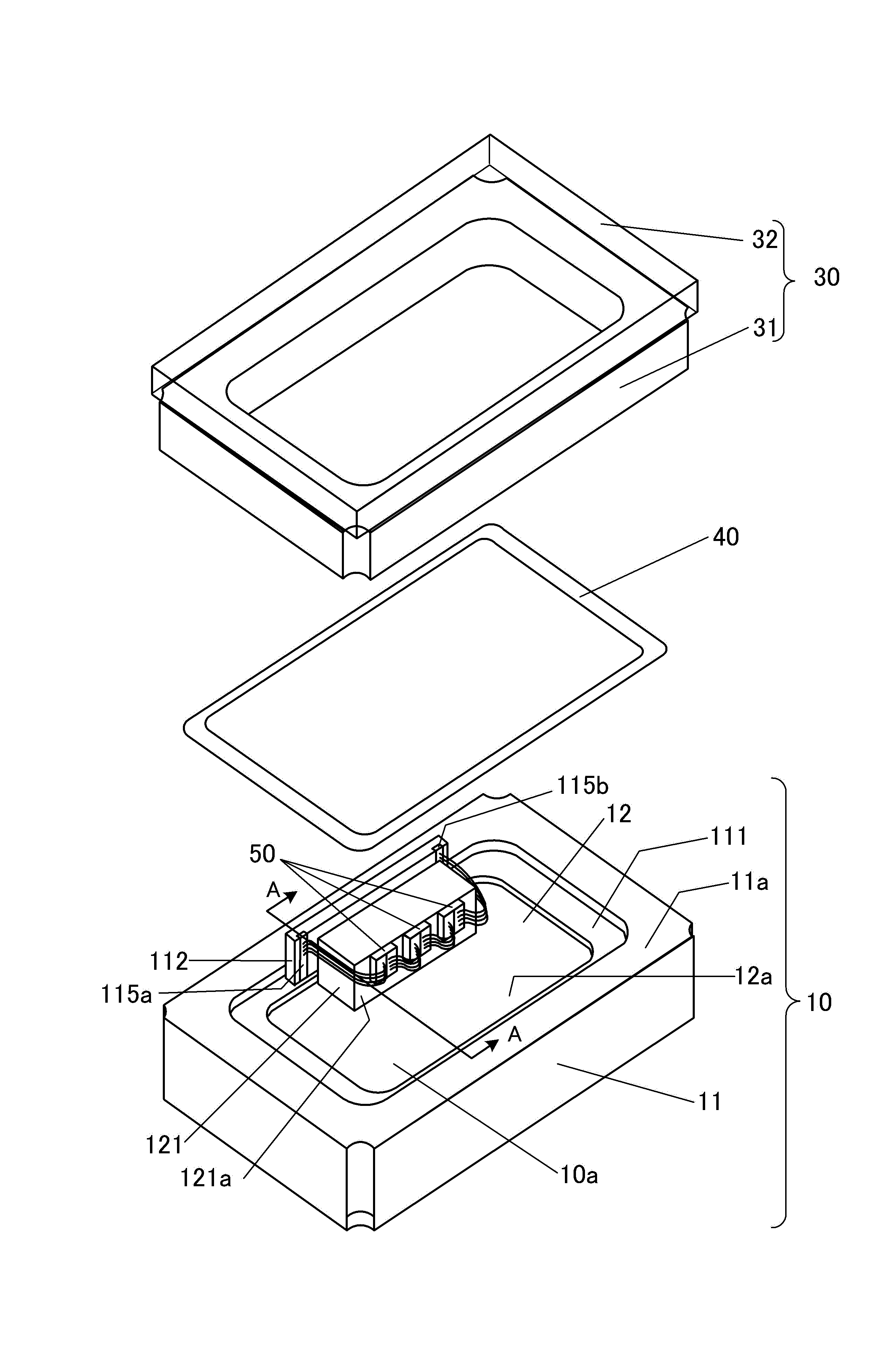
図1は、第1実施形態の発光装置1の全体斜視図である。図2は、発光装置1の本体10と蓋体30とを分解した斜視図である。
発光装置1は、本体10と、蓋体30と、光素子50などを備える。
Hereinafter, an embodiment will be described with reference to the drawings.
[First embodiment]
Fig. 1 is an overall perspective view of a
The
本体10は、光素子50を内部に収容する光素子搭載用パッケージの筐体である。蓋体30は、本体10の内部の光素子50を封止する。蓋体30は、枠体31の上面に光透過性の平板32が位置しており、ここでは、平板32を介して本体10内部の光素子50から光が出射可能となっている。蓋体30は、光素子搭載用パッケージに含まれていてもよいし、本体10のみの光素子搭載用パッケージとは独立して頒布されるものであってもよい。
The
本体10は、枠体11と基体12とを有する。基体12は、上下が開放された枠体11の下端(第1端)側を塞いで枠体11の内部に位置している。基体12は、伝熱体であり、枠体11よりも熱伝導率が高い。例えば、基体12は、銅若しくはアルミニウム、又はこれらのうち少なくともいずれかを含む合金などの金属部材である。あるいは、基体12は、セラミック材であってもよい。また、単結晶性の無機物が基体12に好適に用いられてもよい。さらに、基体12は、無機物と金属との複合物により高熱伝導率が得られるものであってもよい。すなわち、基体12の電気伝導性の有無は問われない。
The
枠体11は、絶縁性を有する。枠体11は、例えば、アルミナ、窒化アルミニウム、窒化ケイ素、ジルコニア、樹脂などである。したがって、枠体11の主成分としてセラミック、特に、アルミナが用いられる場合には、セラミック以外が用いられる場合と比べて、枠体11の気密性が高くなる。また、枠体11の主成分としてセラミックが用いられる場合には、基体12との熱膨張率の差をセラミック以外が用いられる場合と比べて小さくできる。枠体11は、複数の層が積層された構造であってもよい。各層には、枠体11を厚さ方向に貫くビア導体118が位置して、互いに接続している。
The
枠体11は、内側面から内側に向けて環状の突起部111を有する。突起部111は、枠体11と一体構造であり、かつ同一の材質である。突起部111の下面側に基体12の上面12aの周縁部分が接合されている。
The
枠体11の内側面と基体12の上面12a(第1面)とにより囲まれて凹部10a(空間)が位置する。基体12の上面12aから凹部10aに対して、突出部121が突出している。突出部121は、例えば、直方体形状である。突出部121の上面12aからの高さは、上面12aから枠体11の上端までの高さよりも高い。突出部121は、基体12と一体構造かつ同一の材質である。突出部121の周囲は、上面と上記突起部111とにより段状になっている。
The
突出部121のうち上面12aと交差する、すなわち直交する側面の一面は、光素子50の搭載面121a(第2搭載面)である。搭載面121aは、突出部121のうち凹部10aの中心に向いた面とされている。搭載面121aには、1又は複数個の光素子50を接着、搭載することができる。例えば、搭載面121aには、3個の光素子50が位置している。光素子50は、端面発光型のレーザーダイオード(LD)である。光素子50は、その長辺に沿って突出部121と接触している。これにより、光素子50は、動作時に蓋体30を通って外向きに光を出射するとともに、生じた熱が速やかに伝熱体である突出部121を経て基体12へ伝えられる。
One of the sides of the
ここでは、光素子50は、上面12aに対して垂直上向き(上面12aとは反対向き)に光を出射するように位置しているが、これに限られない。光素子50は、上面12aに対して多少斜めの向きで光を出射するのであってもよい。
Here, the
3個の光素子50は、直列に接続され、両端が電極115a、115bに接続されている。光素子50間及び光素子50と電極115a、115bとの間は、ボンディングワイヤにより接続されている。ボンディングワイヤは、例えば、4組が並列に電極115a、光素子50及び電極115bの間を接続している。複数組のボンディングワイヤにより接続されることで、1組が断線しても他の組のボンディングワイヤにより光素子50を発光動作させることができる。
The three
電極115a、115bは、突起部111上に位置する支持台112の側面に露出している。支持台112は、突出部121の搭載面121aとは反対側の面と、枠体11の内側面との間に位置する。支持台112は、枠体11とは別体であってもよい。すなわち、支持台112は、枠体11に対して接合されている。接合は、シンタリングペーストなどにより行われ得る。支持台112は、内部に電極115a、115bにそれぞれつながる配線構造を有する。支持台112の配線構造以外の部分は、絶縁材であり、例えば、枠体11と同一であってもよい。
The
このとき、電極115a、115bは、搭載面121aと正対する側から見た平面視で、搭載面121a及び光素子50と同時に視認可能な位置にある。特に、電極115a、115bを含む面は、搭載面121aに沿った方向であるのが好ましい。沿った方向とは、互いに平行であるか、又は平行方向から若干ずれた範囲内であることを意味する。具体的には、2つの面のなす角度が±30度以下、より好ましくは±20度以下、更に好ましくは±10度以下である。配線構造は、後述のように枠体11の配線構造と接続されて、枠体11の下面に位置する外部電極と電気的につながっている。
At this time, the
枠体11の上面11a(第2端)は、蓋体30が接合可能な第1搭載面となっている。別個の本体10及び蓋体30は、搭載面121aに光素子50が搭載されて、ボンディングワイヤWにより光素子50と電極115a、115bとが接続された後に接合される。これにより、光素子50を含む凹部10aが封止される。このとき、凹部10a内には、乾燥空気又は不活性ガスが充填されてもよい。
The
蓋体30は、上述のように、枠体31と、平板32とを有する。枠体31は、本体10の枠体11と同一の部材であってもよく、すなわち、例えばアルミナである。枠体31の外周形状は、枠体11の外周形状と同一である。枠体31の内周形状は、枠体11の内周形状と同一でなくてもよい。枠体31の高さは、蓋体30により凹部10aを封止した際に、突出部121の上面及び光素子50の発光端と平板32の下面とが接触しない範囲でこれらの幅が十分に小さくなるように定められている。これにより、光素子50が発した光は、蓋体30の厚さに応じた光路長となる。光路長、特に凹部10aの内部における光路長が短いことで、出射光の拡散が抑えられる。これに応じて、突出部121がなく、上面12a付近から出射された光の凹部10aの内部における光路長が本実施形態の光路長よりも長い場合に比して、各出射光の間で干渉が生じにくくなる。したがって、搭載面121aに搭載される複数の光素子50の間隔を狭くすることができる。光素子50の間隔に応じて、光素子搭載用パッケージの平面視サイズも小型化され得る。
As described above, the
平板32は、気密性を有する光透過性の部材であり(透光部分)、例えば、ホウケイ酸ガラス又はサファイアガラスである。平板32の表面は、反射防止コーティング(ARコート)されていてもよい。平板32は、例えば、フリットガラスを用いて枠体31と接合されている。
The
本体10と蓋体30とは、接合部材40を介して接合され得る。接合部材40には、例えば、金すずなどが用いられる。金すずは、例えば、各枠体11、31よりも幅の狭い環状のプリフォームがシールリングとして用いられ得る。
The
あるいは、接合には、フリットガラスなどが用いられてもよい。この場合、接合時に上記蓋体30における枠体31と平板32との接合面が再溶融しないように、蓋体30のフリットガラスよりも低融点のものが用いられる。低融点のフリットガラスは、例えば、金属としてテリリウム、ビスマス、バナジウムなどの混合物を含む。
Alternatively, frit glass or the like may be used for bonding. In this case, a material with a lower melting point than the frit glass of the
図3は、断面線AAにおける本体10の断面図である。
電極115aを含むこの断面図では、電極115aと枠体11の底面に位置する外部接続電極117との間で配線部材がつながっている。
FIG. 3 is a cross-sectional view of the
In this cross-sectional view including the
具体的には、枠体11内には、複数のビア導体118が重なっており、突起部111の上面に位置する接続配線119につながっている。電極115aは、支持台112の内部を伸びる配線部材116(配線導体)と接続している。配線部材116は、支持台112の下端から露出して接続配線119と接続されている。すなわち、配線部材116、外部接続電極117、ビア導体118及び接続配線119を含む配線導体が、ボンディングワイヤWにより電極115aに接続された光素子50を外部と接続する。
Specifically, multiple via
このように、光素子50からの放熱経路は、主に基体12であるのに対し、光素子50との電気的な経路は、枠体11である。すなわち、放熱経路と電気的な経路は分離されている。この結果、電気的な経路が大きな温度変化を生じづらく、これに伴って電気的な経路の抵抗値などの変化が抑えられる。一方、上記のように、放熱経路は、幅が広く、かつ熱伝導率が顕著に高い。したがって、速やかに光素子50から放熱される。
In this way, the heat dissipation path from the
[第2実施形態]
図4は、第2実施形態の本体101を示す斜視図(図4(a))と、断面線AAにおける断面図(図4(b))である。
本体101は、支持台112を有さない。本体101は、電極115a、115bの代わりに単独で直立する電極柱(ピラー115c、115d)を有する。ピラー115c、115dの突起部111との接触部分は、安定性のために太くなっていてもよい。ピラー115c、115dの形状は、任意である。しかしながら、ボンディングワイヤWの接合部分が部分的に平面かつ搭載面121aと略平行であることで、ワイヤボンディングの作業が容易になる。
[Second embodiment]
4A is a perspective view showing a
The
ピラー115c、115dは、例えば、銀ろうなどのろう材を用いて接続配線119と電気的に接続された状態で固定されればよい。
The
[第3実施形態]
図5は、第3実施形態の発光装置1bを示す斜視図(図5(a))と、発光装置1bの蓋体302及び本体102を分離して示す分解斜視図(図5(b))である。
[Third embodiment]
5A is a perspective view showing a
この発光装置1bは、蓋体302がキャップ形状の筐体312と、筐体312の上面に空いた開口を封止する平板322とを有する。平板322は、図示のように開口の外側に接合されていてもよいし、開口の内側に接合されていてもよい。あるいは、平板322は、開口の縁に沿って嵌め込まれていてもよい。開口のサイズは、光素子50の出射光が妨げられずに出射可能な範囲であればよい。このような3次元形状を有する筐体312は、例えば、絞り加工により金属部材が成型されて得られてもよい。
This
本体102は、枠体11の上端面に環状の金属枠材13が位置している点を除き、上記第1実施形態の本体10と同一である。同一の構成には同一の符号を付して詳しい説明を省略する。金属枠材13は、例えば、低抵抗なもの、例えば、コバール(登録商標)である。金属枠材13は、平面視で筐体312の下端が本体102に接する位置と重なっており、すなわち、筐体312の下端と金属枠材13とが接合される。筐体312及び金属枠材13がいずれも低抵抗金属であるので、これらは、シーム溶接により接合されてもよい。
The
[第4、第5実施形態]
図6は、第4、第5実施形態の発光装置1c、1dを示す斜視図である。なお、ここでは、発光装置1cにおける凹部10a内の構成の表記を省略している。
図6(a)に示す第4実施形態の発光装置1cは、上記第1実施形態の発光装置1における蓋体30の平板32上にレンズ構造33が位置している。図6(b)に示す第5実施形態の発光装置1dは、第3実施形態の発光装置1bにおける蓋体302の平板322の上部にレンズ構造33dが位置している。
[Fourth and Fifth Embodiments]
6 is a perspective view showing light emitting devices 1c and 1d according to the fourth and fifth embodiments, in which the configuration inside the
In the light emitting device 1c of the fourth embodiment shown in Fig. 6(a), a
レンズ構造33、33dは、光素子50から各々出射された光の拡散を低減し、更に平行光としたり、収束させたりするコリメートレンズ構造を有する。レンズ構造33は、平板32(透光部分)と別個のものが平板32に接合されたものであるが、平板32と一体的に構成されていてもよい。レンズ構造33dは、平板322と一体的に構成されているものであるが、平板322とは別個の構成が、当該平板322に接合されてもよい。なお、レンズ構造33、33dの収束率は、ある軸方向とこれに垂直な軸方向とで異なっていてもよい。ここでは、レンズ構造33、33dは、主に発光装置1c、1dの長辺方向について出射光を収束させているが、これに限られない。
[第6実施形態]
図7は、第6実施形態の本体103を示す斜視図及び断面図である。
図7(b)は、図7(a)における断面線BBにおける断面図である。また、この図7(b)には、発光装置1が取り付けられる回路基板7の断面が併せて示されている。
図7(a)に示すように、光素子50の一端は、ボンディングワイヤを介さずに直接突出部121と導通している。上記のように、突出部121を含む基体12は、銅など電気伝導性を有するものであってもよい。
Sixth Embodiment
FIG. 7 is a perspective view and a cross-sectional view showing a
Fig. 7(b) is a cross-sectional view taken along line BB in Fig. 7(a) . Fig. 7(b) also shows a cross section of a
7A, one end of the
図7(b)に示すように、基体12の下面には、外部電極124が位置していてもよい。外部電極124は、回路基板7の電極パッド又は接地面などの導体層71と接続され得る。導体層71は、例えば、銅である。回路基板7は、例えば、メタルコア印刷配線板(MCPCB)であってもよい。MCPCBの導体層71は、基体12の下面と接する突起部を有する。この突起部上面には、酸化防止膜としてのめっき層が位置していてもよい。めっきは、例えば、Niめっき又はAuめっきなどである。MCPCBの導体層71は、絶縁体72により上下方向に分離されている。絶縁体72は、例えば、高い熱伝導率を有する絶縁性フィラーを含有する有機接着剤などである。したがって、熱は、絶縁体72を貫通して更に下方に流れ得る。下層の導体層71は、ヒートシンクとなる。一方導体層71に沿った電流は、回路基板7の上面側の導体層71に限られて流れる。すなわち、上層の導体層71は、配線層である。配線のパターンエッジは、ソルダーレジストで覆われていてもよい。図7(b)の断面外にある外部接続電極117に接続する回路基板7上の配線導体は、絶縁体73によって導体層71と離隔している。
7B, an
この第6実施形態の本体103のように、発光装置1からの放熱経路と、一方の電気経路とが部分的に共通していてもよい。
As in the
[第7実施形態]
図8は、第7実施形態の本体104を示す断面図である。
この断面は、図2における断面線AAと同一である。
[Seventh embodiment]
FIG. 8 is a cross-sectional view showing a
This section is identical to section line AA in FIG.
本体104は、第1実施形態の本体10における基体12が突出部121の代わりに突出部1211を有する。その他の構成及び構造は同一である。突出部1211は、光素子50の搭載面121aが上面12aに対して傾斜している。傾斜角度は、光素子50からの出射光が蓋体30の外側に至るまでの光路が大きく延長されない範囲であればよく、例えば、45度以上90度以下である。ここでいう傾斜角度は、搭載面121aが上面12aに対してなす2つの角度のうち小さい方であってもよい。
In the
図9は、発光装置1cを回路基板7上に複数配置した例を示す図である。
上記のように、発光装置1c自体が従来よりも小型化され得るので、全体として必要な発光量、すなわち発光装置1cの数に比して、回路基板7のサイズが小型化され得る。また、回路基板7上で複数の発光装置1cが密に配置され得る。
FIG. 9 is a diagram showing an example in which a plurality of light emitting devices 1 c are arranged on a
As described above, the light emitting device 1c itself can be made smaller than before, so that the size of the
以上のように、本実施形態の光素子搭載用パッケージの本体10は、絶縁性の枠体11と、枠体11の下端を塞いで位置し、枠体11よりも熱伝導率の高い基体12と、枠体11及び基体12に囲まれた凹部10aに対して基体12の上面12aから突出する突出部121と、を備える。枠体11は、その下端とは反対の上端側に透光部分を有する蓋体30が接合可能な上面11aを有する。突出部121は、上面12aと交差しており、端面発光型の光素子50を搭載可能な搭載面121aを有する。
このように、光素子搭載用パッケージの本体10は、上面発光型などと比較して発光効率が高く発光強度を得られる端面発光型の光素子50を蓋体30に直接向くように搭載可能なので、当該パッケージの外へ出射された直後の出射光の拡散が進まない。したがって、鏡面により光素子50の発した光を蓋体30の方向に反射させて外部に出射させる場合に比して、この光素子搭載用パッケージを用いた発光装置1における発光特性の低下が抑えられる。特に、複数の発光装置1からの出射光間で干渉しにくくなるので、複数の光素子搭載用パッケージが従来よりも近接配置され得る。また、このような向きの光素子50が突出部121の側面である搭載面121aに接して位置するので、光素子50が安定して支持される。さらに、突出部121により、光素子50と搭載面121aとの接触面積が大きくなるので、本体10は、光素子50の発した熱を速やかに突出部121へ逃がすことができる。よって、本体10は、光素子50の過熱による劣化や故障を低減させることができる。
As described above, the
In this way, the
また、突出部121は、基体12の少なくとも一部と一体構造であり、この一体構造部分は、基体12の上下面にわたって貫通している。これにより、光素子搭載用パッケージの本体10は、光素子50が発した熱を突出部121を含む基体12を経て速やかに基体12の下面側から放出することができる。
The
また、前記搭載面121aは、上面12aに対して45度以上90度以下の範囲で交差していてもよい。すなわち、光素子50は、上面12aの法線方向、すなわち直上に光を出射する場合に限られない。これにより、本体10は、用途などに応じて柔軟な向きに光を出射させることができる。一方で、傾斜角が小さくなりすぎないことで、光素子50において端面発光した光が蓋体30を通過する光路長が著しく長くならない範囲に留められる。したがって、この本体10は、発光装置1における発光特性の低下が抑えられる。
The mounting
また、搭載面121aには、複数の光素子50が搭載可能であってもよい。光素子50の出射光が蓋体30を通過するまでの光路長が短いことで、出射光の拡散が進まず、互いに干渉するのが避けられる。したがって、この本体10は、光素子50の搭載位置の間隔を従来よりも小さくすることができる。すなわち、本体10は、搭載可能な光素子50の数に比して小型化され得る。
Moreover, multiple
また、枠体11は、光素子50と外部とを接続する配線導体として、配線部材116、外部接続電極117、ビア導体118及び接続配線119を有する。すなわち、電気信号や供給電力は、枠体11内を通って外部から供給される。したがって、突出部121を含む基体12を主に伝わる熱流と経路が分離され、電気信号が熱の影響を直接受けにくくなる。
The
また、枠体11は、配線導体と電気的につながっている電極115a、115bが露出されている。電極115a、115bを含む面は、搭載面121aに沿った方向である。このように、ボンディングワイヤWにより接続される電極115a、115bと、搭載面121a上の光素子50の端子とが、略同一方向を向いていることで、ワイヤボンディングの際にキャピラリが二次元的な動作で済む。したがって、ワイヤボンディングが容易になり、手間やコストの低減が図られる。
The
特に、搭載面121aに正対する側から見た場合に、搭載面121aと電極115a、115bとが同時に視認可能であり、かつ、枠体11のうち突出部121に対して電極115a、115bのある側とは反対側の上面11aの上面12aからの高さは、突出部121の上面12aからの高さよりも低い。これにより、ワイヤボンディングの際にキャピラリの本体10の外から中への移動も二次元的な移動で留めることができる。よって、この本体10は、より容易なワイヤボンディングにより低コストで得られる。
In particular, when viewed from the side directly opposite the mounting
また、基体12は、アルミニウム若しくは銅、又はこれらのうち少なくともいずれかを含む合金であってもよい。すなわち、基体12は、熱伝導率が高く、かつ低コストであるものが好ましい。これにより、本体10は、光素子50の発する熱を速やかに外部へ放出することができる。
The base 12 may also be aluminum or copper, or an alloy containing at least one of these. In other words, the
また、枠体11は、セラミックであるとよい。枠体11は、絶縁体であるとともに、気密性の高い材質であることが好ましい。よって、枠体11がセラミックであることで、高い気密性を得ることができる。
Furthermore, it is preferable that the
さらに、セラミックはアルミナであってもよい。熱伝導率の高い基体12は、熱膨張率も高いことが多い。この熱膨張率に対して、枠体11の熱膨張率の差が大きいと、枠体11と基体12との間で大きな歪みが生じやすくなり、本体10の劣化が促される。したがって、安価なセラミックとしては比較的熱膨張率の大きいアルミナが枠体11に用いられることで、本体10の劣化を低減させることができる。
Furthermore, the ceramic may be alumina. A base 12 with a high thermal conductivity often also has a high coefficient of thermal expansion. If there is a large difference in the thermal expansion coefficient of the
また、光素子搭載用パッケージは、光素子50の発する光が透過する透光部分である平板32を有し、上面11aに接合可能な蓋体30を備えていてもよい。光素子搭載用パッケージとして本体10及び蓋体30をセットで頒布することで、光素子50を本体10に搭載した後に好適な組み合わせの蓋体30により、光素子50が封止される。
The package for mounting an optical element may have a
また、平板32上にレンズ構造が位置していたり、平板32の代わりにレンズ構造を有する光透過性部材が用いられたりしてもよい。初めから光素子搭載用パッケージの出射光を平行光などに変換するレンズ構造を有することで、出射光に対する公的なレンズの選択、取得、及び取付時の光軸調整などが不要になる。したがって、この光素子搭載用パッケージにより、ユーザの利便性が向上する。
Also, a lens structure may be located on the
また、本実施形態の発光装置1は、上記の光素子搭載用パッケージとしての本体10と、搭載面121aに搭載される光素子50と、光素子50の発する光が透過する平板32を有し、上面11aに接合可能な蓋体30と、を備える。光素子50は、平板32を介して光素子搭載用パッケージの外へ光を出射する向きで、搭載面121aに搭載される。
このように、本実施形態の発光装置1は、端面発光の光素子50を直接上方に出射させることができる。したがって、光素子50の発した光が蓋体30の外に出射されるまでの光路長を短くすることができる。その結果、発光装置1は、光学特性の低下が抑えられる。
The
In this way, the
なお、上記実施の形態は例示であって、様々な変更が可能である。
例えば、突出部121は、必ずしも基体12と一体構造ではなくてもよい。これらが別体である場合には、両者の間は、熱伝導率の高いろう材、はんだ、シンタリング材などにより接合され得る。また、この場合、突出部121は、基体12上に載っているものではなくてもよい。基体12の上面12aに位置する孔内に半分埋め込まれた形状などであってもよい。この孔は、基体12を貫通していてもよい。
The above-described embodiment is merely an example, and various modifications are possible.
For example, the
また、この場合、突出部121は、基体12とは異なる材質であってもよい。この場合であっても、突出部121と基体12との間で高い熱伝導率で熱が伝わることがより好ましい。
In this case, the
また、上記では、二次元的なワイヤボンディングを考慮して電極115a、115bやピラー115c、115dの位置や形状が定められた。しかしながら、二次元的なワイヤボンディングに限らなければ、電極115a、115b及びピラー115c、115dの位置や形状は、上記に限られない。
In addition, in the above, the positions and shapes of the
また、上記では、4本のボンディングワイヤWが並列に接続されるものとして説明したが、これに限られない。他の本数であってもよい。あるいは、ワイヤの代わりに帯状(リボン状)の導体がボンディングされて電極及び端子間が接続されてもよい。 In addition, in the above description, four bonding wires W are connected in parallel, but this is not limited to this. Any other number of wires may be used. Alternatively, a band-shaped (ribbon-shaped) conductor may be bonded instead of wires to connect between the electrodes and terminals.
また、第6実施形態では、一本の信号経路のみが導体である基体12を通るものとして説明したが、これに限られない。絶縁体の基体12に2本の信号経路が通っており、ボンディングワイヤWが全く用いられず、枠体11が配線経路を有さなくてもよい。この場合には、逆に、枠体11が電気伝導性の材質であってもよい。
In the sixth embodiment, only one signal path passes through the
また、ビア導体118に加えて又は代えてキャスタレーションや側面電極などが用いられてもよい。
In addition to or instead of the via
また、突出部121の搭載面121a及び支持台112の電極115a、115bを含む面以外の形状は、上記の実施の形態で示したものに限られない。これらは、他の形状を有していてもよい。
Furthermore, the shapes of the mounting
また、ある光素子搭載用パッケージに搭載される複数の光素子50には、互いに異なる波長の光を発光するものが含まれていてもよい。例えば、赤色発光のLDと青色発光のLDとが同一の光素子搭載用パッケージに搭載されていてもよい。
The
また、第3実施形態及び第5実施形態の光素子搭載用パッケージでは、蓋体30における平板322が筐体312の略中央に位置したが、これに限られない。光素子50の搭載位置に応じて偏った位置にあってもよい。
その他、上記実施の形態で示した構成、構造、位置関係、材質などの具体的な細部は、本開示の趣旨を逸脱しない範囲において適宜変更可能である。本発明の範囲は、特許請求の範囲に記載した発明の範囲とその均等の範囲を含む。
In the optical element mounting packages according to the third and fifth embodiments, the
In addition, the specific details of the configuration, structure, positional relationship, materials, etc. shown in the above embodiment can be appropriately changed without departing from the spirit of the present disclosure. The scope of the present invention includes the scope of the invention described in the claims and its equivalents.
1、1b~1d 発光装置
10、101~104 本体
10a 凹部
11 枠体
11a 上面
111 突起部
112 支持台
115a、115b 電極
115c、115d ピラー
116 配線部材
117 外部接続電極
118 ビア導体
119 接続配線
12 基体
12a 上面
121、1211 突出部
121a 搭載面
124 外部電極
13 金属枠材
30、302 蓋体
31 枠体
312 筐体
32、322 平板
33、33d レンズ構造
40 接合部材
50 光素子
7 回路基板
71 導体層
72、73 絶縁体
W ボンディングワイヤ
Claims (13)
前記枠体の第1端を塞いで位置し、前記枠体よりも熱伝導率の高い伝熱体と、
前記枠体及び前記伝熱体に囲まれた空間に対して前記伝熱体の第1面から突出する突出部と、
を備え、
前記枠体は、前記第1端とは反対の第2端側に透光部分を有する蓋体が接合可能な第1搭載面を有し、
前記突出部は、前記第1面と交差しており、端面発光型の光素子を搭載可能な第2搭載面を有する、
光素子搭載用パッケージ。 An insulating frame;
a heat transfer body that is positioned to close a first end of the frame body and has a higher thermal conductivity than the frame body;
a protrusion protruding from a first surface of the heat transfer body into a space surrounded by the frame and the heat transfer body;
Equipped with
the frame body has a first mounting surface to which a lid body having a light-transmitting portion can be joined on a second end side opposite to the first end,
the protrusion intersects with the first surface and has a second mounting surface on which an edge-emitting optical element can be mounted;
A package for mounting optical elements.
前記電極を含む面は、前記第2搭載面に沿った方向である、請求項5記載の光素子搭載用パッケージ。 The frame has an exposed electrode electrically connected to the wiring conductor,
6. The optical element mounting package according to claim 5, wherein the surface including the electrodes is in a direction parallel to the second mounting surface.
前記第2搭載面に搭載される光素子と、
前記光素子の発する光が透過する透光部分を有し、前記第1搭載面に接合可能な蓋体と、
を備え、
前記光素子は、前記透光部分を介して前記光素子搭載用パッケージの外へ光を出射する向きで、前記第2搭載面に搭載される
発光装置。 An optical element mounting package according to any one of claims 1 to 10,
an optical element mounted on the second mounting surface;
a cover body having a light transmitting portion through which light emitted by the optical element passes and which can be joined to the first mounting surface;
Equipped with
the optical element is mounted on the second mounting surface in a direction in which light is emitted to the outside of the optical element mounting package through the light-transmitting portion.
Priority Applications (2)
| Application Number | Priority Date | Filing Date | Title |
|---|---|---|---|
| JP2023107841A JP2025006830A (en) | 2023-06-30 | 2023-06-30 | Package for mounting optical element and light emitting device |
| PCT/JP2024/023295 WO2025005172A1 (en) | 2023-06-30 | 2024-06-27 | Package for mounting optical element, and light-emitting device |
Applications Claiming Priority (1)
| Application Number | Priority Date | Filing Date | Title |
|---|---|---|---|
| JP2023107841A JP2025006830A (en) | 2023-06-30 | 2023-06-30 | Package for mounting optical element and light emitting device |
Publications (1)
| Publication Number | Publication Date |
|---|---|
| JP2025006830A true JP2025006830A (en) | 2025-01-17 |
Family
ID=93939102
Family Applications (1)
| Application Number | Title | Priority Date | Filing Date |
|---|---|---|---|
| JP2023107841A Pending JP2025006830A (en) | 2023-06-30 | 2023-06-30 | Package for mounting optical element and light emitting device |
Country Status (2)
| Country | Link |
|---|---|
| JP (1) | JP2025006830A (en) |
| WO (1) | WO2025005172A1 (en) |
Citations (4)
| Publication number | Priority date | Publication date | Assignee | Title |
|---|---|---|---|---|
| JP2008258438A (en) * | 2007-04-05 | 2008-10-23 | Nichia Corp | Semiconductor light emitting device |
| JP2018107348A (en) * | 2016-12-27 | 2018-07-05 | 日亜化学工業株式会社 | Light emitting device |
| JP2020113718A (en) * | 2019-01-16 | 2020-07-27 | 日亜化学工業株式会社 | Light-emitting device and method for manufacturing the same |
| JP2022187270A (en) * | 2021-06-07 | 2022-12-19 | ヌヴォトンテクノロジージャパン株式会社 | Light-emitting device |
-
2023
- 2023-06-30 JP JP2023107841A patent/JP2025006830A/en active Pending
-
2024
- 2024-06-27 WO PCT/JP2024/023295 patent/WO2025005172A1/en not_active Ceased
Patent Citations (4)
| Publication number | Priority date | Publication date | Assignee | Title |
|---|---|---|---|---|
| JP2008258438A (en) * | 2007-04-05 | 2008-10-23 | Nichia Corp | Semiconductor light emitting device |
| JP2018107348A (en) * | 2016-12-27 | 2018-07-05 | 日亜化学工業株式会社 | Light emitting device |
| JP2020113718A (en) * | 2019-01-16 | 2020-07-27 | 日亜化学工業株式会社 | Light-emitting device and method for manufacturing the same |
| JP2022187270A (en) * | 2021-06-07 | 2022-12-19 | ヌヴォトンテクノロジージャパン株式会社 | Light-emitting device |
Also Published As
| Publication number | Publication date |
|---|---|
| WO2025005172A1 (en) | 2025-01-02 |
Similar Documents
| Publication | Publication Date | Title |
|---|---|---|
| JP7364970B2 (en) | light emitting device | |
| JP6048880B2 (en) | LIGHT EMITTING ELEMENT PACKAGE AND LIGHT EMITTING DEVICE USING THE SAME | |
| US8124998B2 (en) | Light emitting device package | |
| JP6986453B2 (en) | Semiconductor laser device | |
| JP2025016616A (en) | METHOD FOR MANUFACTURING LIGHT-EMITTING MODULE, LIGHT-EMITTING MODULE AND PROJECTOR | |
| JP2025006830A (en) | Package for mounting optical element and light emitting device | |
| WO2021125017A1 (en) | Light-receiving element and light-emitting device | |
| JP2013219071A (en) | Light-emitting element mounting component and light-emitting device | |
| US20240405506A1 (en) | Light-emitting module, mounting substrate, and manufacturing method of mounting substrate | |
| WO2019073853A1 (en) | Optical device and system | |
| JP2021028919A (en) | Semiconductor laser device | |
| JP6910976B2 (en) | Optical module | |
| JP2006108432A (en) | Light emitting element storage package | |
| JP2024065281A (en) | Light emitting device and method for manufacturing the same |
Legal Events
| Date | Code | Title | Description |
|---|---|---|---|
| A621 | Written request for application examination |
Free format text: JAPANESE INTERMEDIATE CODE: A621 Effective date: 20250724 |
|
| A131 | Notification of reasons for refusal |
Free format text: JAPANESE INTERMEDIATE CODE: A131 Effective date: 20260310 |