JP2023513195A - button composite structure - Google Patents
button composite structure Download PDFInfo
- Publication number
- JP2023513195A JP2023513195A JP2022547905A JP2022547905A JP2023513195A JP 2023513195 A JP2023513195 A JP 2023513195A JP 2022547905 A JP2022547905 A JP 2022547905A JP 2022547905 A JP2022547905 A JP 2022547905A JP 2023513195 A JP2023513195 A JP 2023513195A
- Authority
- JP
- Japan
- Prior art keywords
- button
- substrate
- composite structure
- display panel
- light emitting
- Prior art date
- Legal status (The legal status is an assumption and is not a legal conclusion. Google has not performed a legal analysis and makes no representation as to the accuracy of the status listed.)
- Granted
Links
Images


Classifications
-
- H—ELECTRICITY
- H01—ELECTRIC ELEMENTS
- H01H—ELECTRIC SWITCHES; RELAYS; SELECTORS; EMERGENCY PROTECTIVE DEVICES
- H01H13/00—Switches having rectilinearly-movable operating part or parts adapted for pushing or pulling in one direction only, e.g. push-button switch
- H01H13/02—Details
- H01H13/12—Movable parts; Contacts mounted thereon
- H01H13/14—Operating parts, e.g. push-button
-
- H—ELECTRICITY
- H01—ELECTRIC ELEMENTS
- H01H—ELECTRIC SWITCHES; RELAYS; SELECTORS; EMERGENCY PROTECTIVE DEVICES
- H01H13/00—Switches having rectilinearly-movable operating part or parts adapted for pushing or pulling in one direction only, e.g. push-button switch
- H01H13/70—Switches having rectilinearly-movable operating part or parts adapted for pushing or pulling in one direction only, e.g. push-button switch having a plurality of operating members associated with different sets of contacts, e.g. keyboard
-
- G—PHYSICS
- G06—COMPUTING OR CALCULATING; COUNTING
- G06F—ELECTRIC DIGITAL DATA PROCESSING
- G06F3/00—Input arrangements for transferring data to be processed into a form capable of being handled by the computer; Output arrangements for transferring data from processing unit to output unit, e.g. interface arrangements
- G06F3/01—Input arrangements or combined input and output arrangements for interaction between user and computer
- G06F3/03—Arrangements for converting the position or the displacement of a member into a coded form
- G06F3/033—Pointing devices displaced or positioned by the user, e.g. mice, trackballs, pens or joysticks; Accessories therefor
- G06F3/039—Accessories therefor, e.g. mouse pads
- G06F3/0393—Accessories for touch pads or touch screens, e.g. mechanical guides added to touch screens for drawing straight lines, hard keys overlaying touch screens or touch pads
-
- G—PHYSICS
- G02—OPTICS
- G02F—OPTICAL DEVICES OR ARRANGEMENTS FOR THE CONTROL OF LIGHT BY MODIFICATION OF THE OPTICAL PROPERTIES OF THE MEDIA OF THE ELEMENTS INVOLVED THEREIN; NON-LINEAR OPTICS; FREQUENCY-CHANGING OF LIGHT; OPTICAL LOGIC ELEMENTS; OPTICAL ANALOGUE/DIGITAL CONVERTERS
- G02F1/00—Devices or arrangements for the control of the intensity, colour, phase, polarisation or direction of light arriving from an independent light source, e.g. switching, gating or modulating; Non-linear optics
- G02F1/01—Devices or arrangements for the control of the intensity, colour, phase, polarisation or direction of light arriving from an independent light source, e.g. switching, gating or modulating; Non-linear optics for the control of the intensity, phase, polarisation or colour
- G02F1/13—Devices or arrangements for the control of the intensity, colour, phase, polarisation or direction of light arriving from an independent light source, e.g. switching, gating or modulating; Non-linear optics for the control of the intensity, phase, polarisation or colour based on liquid crystals, e.g. single liquid crystal display cells
- G02F1/133—Constructional arrangements; Operation of liquid crystal cells; Circuit arrangements
- G02F1/1333—Constructional arrangements; Manufacturing methods
- G02F1/133308—Support structures for LCD panels, e.g. frames or bezels
-
- G—PHYSICS
- G06—COMPUTING OR CALCULATING; COUNTING
- G06F—ELECTRIC DIGITAL DATA PROCESSING
- G06F3/00—Input arrangements for transferring data to be processed into a form capable of being handled by the computer; Output arrangements for transferring data from processing unit to output unit, e.g. interface arrangements
- G06F3/01—Input arrangements or combined input and output arrangements for interaction between user and computer
- G06F3/02—Input arrangements using manually operated switches, e.g. using keyboards or dials
- G06F3/0202—Constructional details or processes of manufacture of the input device
-
- H—ELECTRICITY
- H01—ELECTRIC ELEMENTS
- H01H—ELECTRIC SWITCHES; RELAYS; SELECTORS; EMERGENCY PROTECTIVE DEVICES
- H01H13/00—Switches having rectilinearly-movable operating part or parts adapted for pushing or pulling in one direction only, e.g. push-button switch
- H01H13/02—Details
- H01H13/04—Cases; Covers
- H01H13/06—Dustproof, splashproof, drip-proof, waterproof or flameproof casings
-
- H—ELECTRICITY
- H01—ELECTRIC ELEMENTS
- H01H—ELECTRIC SWITCHES; RELAYS; SELECTORS; EMERGENCY PROTECTIVE DEVICES
- H01H13/00—Switches having rectilinearly-movable operating part or parts adapted for pushing or pulling in one direction only, e.g. push-button switch
- H01H13/70—Switches having rectilinearly-movable operating part or parts adapted for pushing or pulling in one direction only, e.g. push-button switch having a plurality of operating members associated with different sets of contacts, e.g. keyboard
- H01H13/83—Switches having rectilinearly-movable operating part or parts adapted for pushing or pulling in one direction only, e.g. push-button switch having a plurality of operating members associated with different sets of contacts, e.g. keyboard characterised by legends, e.g. Braille, liquid crystal displays, light emitting or optical elements
-
- H—ELECTRICITY
- H01—ELECTRIC ELEMENTS
- H01H—ELECTRIC SWITCHES; RELAYS; SELECTORS; EMERGENCY PROTECTIVE DEVICES
- H01H2219/00—Legends
- H01H2219/054—Optical elements
- H01H2219/062—Light conductor
- H01H2219/0622—Light conductor only an illuminated ring around keys
Landscapes
- Engineering & Computer Science (AREA)
- Physics & Mathematics (AREA)
- General Engineering & Computer Science (AREA)
- Theoretical Computer Science (AREA)
- General Physics & Mathematics (AREA)
- Nonlinear Science (AREA)
- Human Computer Interaction (AREA)
- Crystallography & Structural Chemistry (AREA)
- Chemical & Material Sciences (AREA)
- Mathematical Physics (AREA)
- Optics & Photonics (AREA)
- Push-Button Switches (AREA)
- Devices For Indicating Variable Information By Combining Individual Elements (AREA)
- Liquid Crystal (AREA)
- Switch Cases, Indication, And Locking (AREA)
- Switches With Compound Operations (AREA)
Abstract
一実施形態によるボタン複合構造物は、第1基板、前記第1基板上の第2基板、および前記第1基板と前記第2基板の間の液晶層を含む表示パネルと、前記第2基板上の部材と、前記表示パネルと前記部材の一面を結合する第1結合部材と、前記部材の一面の反対面である他面上に配置されたボタン構造物と、前記部材の他面と前記ボタン構造物を結合する第2結合部材を含み、前記部材は第3基板、および前記第3基板上のタッチ層を含み、前記タッチ層は前記部材の前記一面を含み、前記タッチ層は前記第1結合部材によって前記表示パネルと結合され、前記ボタン構造物は前記第2結合部材によって前記第3基板と直接結合され、前記ボタン構造物は透明導電物質を含む。【選択図】図1A button composite structure according to one embodiment comprises a display panel including a first substrate, a second substrate on the first substrate, and a liquid crystal layer between the first substrate and the second substrate; a first coupling member that couples the display panel and one surface of the member; a button structure disposed on the other surface opposite to the one surface of the member; and the other surface of the member and the button a second coupling member coupling a structure, the member comprising a third substrate and a touch layer on the third substrate, the touch layer comprising the one surface of the member, the touch layer being the first It is coupled with the display panel by a coupling member, the button structure is directly coupled with the third substrate by the second coupling member, and the button structure includes a transparent conductive material. [Selection drawing] Fig. 1
Description
本発明はボタン複合構造物に関する。 The present invention relates to button composite structures.
一般的にボタン構造物はガラス、石英などのリジッド基板を貫通してリジッド基板下部のデッキに締結されることができる。 In general, the button structure can be fastened to a deck under the rigid substrate through a rigid substrate such as glass or quartz.
ただし、ボタン構造物をデッキに締結するためにリジッド基板に貫通孔を開ける過程でリジッド基板の破損が生じ得るだけでなく、コストの消耗も少なくなく、デザイン自由度が大きく落ち得る。 However, the rigid substrate may be damaged during the process of drilling the through hole in the rigid substrate to fasten the button structure to the deck, and the cost is high, and the degree of freedom in design may be greatly reduced.
なお、リジッド基板の下部上には表示パネルが配置されるが、前記リジッド基板の貫通孔による漏水によってボタン構造物だけでなく、表示パネルの不良が発生する場合もある。 In addition, a display panel is disposed on the lower portion of the rigid substrate, and water leakage through the through holes of the rigid substrate may cause defects in the display panel as well as the button structure.
さらに、ボタン構造物はボタン入力信号を収容する回路部をさらに含むが、回路部が故障する場合、ボタン構造物がデッキに締結されて分離されにくい構造であると、前記リジッド基板を分解し故障したボタン構造物をデッキから分離しなければならない。この場合、リジッド基板の分解作業は容易ではない。 In addition, the button structure further includes a circuit unit for receiving button input signals. button structure must be separated from the deck. In this case, the work of disassembling the rigid substrate is not easy.
本発明が解決しようとする課題は、リジッド基板の貫通孔を形成することなくリジッド基板に直接積層されたボタン構造物を含むボタン複合構造物を提供することにある。 SUMMARY OF THE INVENTION The problem to be solved by the present invention is to provide a button composite structure including a button structure directly laminated to a rigid substrate without forming a through hole in the rigid substrate.
本発明の課題は、以上で言及した技術的課題に制限されず、言及されていないまた他の技術的課題は以下の記載から当業者に明確に理解されることができる。 The problems of the present invention are not limited to the technical problems mentioned above, and other technical problems not mentioned can be clearly understood by those skilled in the art from the following description.
前記課題を解決するための一実施形態によるボタン複合構造物は、第1基板、前記第1基板上の第2基板、および前記第1基板と前記第2基板の間の液晶層を含む表示パネルと、前記第2基板上の部材と、前記表示パネルと前記部材の一面を結合する第1結合部材と、前記部材の一面の反対面である他面上に配置されたボタン構造物と、前記部材の他面と前記ボタン構造物を結合する第2結合部材を含み、前記部材は第3基板、および前記第3基板上のタッチ層を含み、前記タッチ層は前記部材の前記一面を含み、前記タッチ層は前記第1結合部材によって前記表示パネルと結合され、前記ボタン構造物は前記第2結合部材によって前記第3基板と直接結合され、前記ボタン構造物は透明導電物質を含む。 A button composite structure according to one embodiment for solving the above problems is a display panel including a first substrate, a second substrate on the first substrate, and a liquid crystal layer between the first substrate and the second substrate. a member on the second substrate; a first coupling member that couples the display panel and one surface of the member; a button structure disposed on the other surface opposite to the one surface of the member; a second coupling member coupling the other surface of the member and the button structure, the member comprising a third substrate and a touch layer on the third substrate, the touch layer comprising the one surface of the member; The touch layer is coupled with the display panel by the first coupling member, the button structure is directly coupled with the third substrate by the second coupling member, and the button structure includes a transparent conductive material.
前記ボタン構造物は前記第3基板に固定されたボタン本体部、前記ボタン本体部と締結されたボタン装着部、および前記ボタン装着部と連結されたボタン部を含み得る。 The button structure may include a button body fixed to the third substrate, a button mounting part coupled to the button body, and a button part connected to the button mounting part.
前記ボタン本体部はロックピンを含み、前記ボタン装着部はロック溝を含み、前記ボタン装着部は前記ロック溝に前記ロックピンが挿入される方式で前記ボタン本体部に締結されるように構成され得る。 The button body includes a lock pin, the button mounting portion includes a lock groove, and the button mounting portion is configured to be fastened to the button body by inserting the lock pin into the lock groove. obtain.
前記ロックピンは複数であり、複数の前記ロックピンはそれぞれ複数のロック解除ピンによって同時に前記ロック溝から抜く方式で前記ボタン本体部と分離されるように構成され得る。 A plurality of the lock pins may be provided, and the plurality of lock pins may be configured to be separated from the button body by simultaneously pulling out the lock grooves by a plurality of unlock pins.
前記ボタン部と前記第3基板の間に配置された導電テープをさらに含み、前記導電テープは前記ボタン部に付着し得る。 A conductive tape may be disposed between the button portion and the third substrate, and the conductive tape may adhere to the button portion.
前記ボタン部に物理的入力が印加されると前記導電テープは前記第3基板に接し、前記ボタン部に物理的入力が印加されないと前記導電テープは前記第3基板から離隔し得る。 The conductive tape may be in contact with the third substrate when a physical input is applied to the button portion, and the conductive tape may be separated from the third substrate when a physical input is not applied to the button portion.
前記ボタン装着部は前記ボタンから遠くなる方向に湾入した湾入部を含み、前記ボタン部は前記湾入部に向かって突出した突出部を含み、前記湾入部と前記突出部の間に配置されたダンパをさらに含み得る。 The button mounting part includes an indented part that is indented in a direction away from the button, and the button part includes a protruding part that protrudes toward the indented part, and is disposed between the indented part and the protruding part. A damper may further be included.
前記部材と前記表示パネルの間に配置された回路基板をさらに含み、前記回路基板上に実装した発光素子がさらに配置され得る。 A circuit board may be further included between the member and the display panel, and a light emitting element mounted on the circuit board may be further arranged.
前記回路基板と電気的に接続された信号配線をさらに含み、前記発光素子は前記信号配線を介して電源の供給を受けるように構成され得る。 A signal wiring electrically connected to the circuit board may be further included, and the light emitting device may be configured to receive power supply through the signal wiring.
前記発光素子は前記ボタン部に入力された入力信号に応じて発光するように構成され得る。 The light emitting element may be configured to emit light according to an input signal input to the button section.
前記信号配線は前記部材と前記表示パネルの間に配置され、前記部材の延長方向に沿って延びて前記第1結合部材を貫通し得る。 The signal wiring may be disposed between the member and the display panel, extend along an extension direction of the member, and pass through the first coupling member.
前記発光素子上に重畳配置され、前記ボタン装着部内に配置された焦点可変部をさらに含み、前記焦点可変部は前記発光素子から提供された光の焦点を可変させるように構成され得る。 It may further include a variable focus unit superimposed on the light emitting device and disposed within the button mount, wherein the variable focus unit is configured to change the focus of light provided from the light emitting device.
その他実施形態の具体的な内容は詳細な説明および図面に含まれている。 Specifics of other embodiments are included in the detailed description and drawings.
一実施形態によるボタン複合構造物によれば、リジッド基板の貫通孔を形成することなくリジッド基板に直接ボタン構造物が積層されることによって、リジッド基板の破損発生を減らし、コストを減らして、デザイン自由度を高めることができる。 According to the button composite structure according to one embodiment, since the button structure is directly laminated on the rigid substrate without forming a through hole in the rigid substrate, damage to the rigid substrate can be reduced, the cost can be reduced, and the design can be reduced. It can increase the degree of freedom.
また、前記貫通孔を形成しないため、漏水による表示パネル、およびボタン構造物の故障を減らすことができる。 Also, since the through holes are not formed, it is possible to reduce damage to the display panel and the button structure due to water leakage.
また、ボタン構造物は前記リジッド基板に固定されたボタン本体部、および回路部を含むボタン回路部を含むことによって回路部が故障する場合、ボタン回路のみを容易に交換することができる。 In addition, since the button structure includes the button body portion fixed to the rigid substrate and the button circuit portion including the circuit portion, when the circuit portion fails, only the button circuit can be easily replaced.
また、ボタン部が導電性物質で実現され、ボタン部がタッチ層を含む部材と静電気タッチ駆動方式で入力信号が生成されるので、ボタン部の入力信号を生成するためのボタンスイッチ、および回路基板を省略することができる。 In addition, since the button part is made of a conductive material and the button part generates an input signal by a member including a touch layer and an electrostatic touch driving method, a button switch and a circuit board for generating the input signal of the button part are provided. can be omitted.
実施形態による効果は、以上で例示した内容によって制限されず、より多様な効果が本明細書内に含まれている。 The effects of the embodiments are not limited by the contents exemplified above, and more various effects are included in this specification.
本発明の利点および特徴、並びにこれらを達成する方法は添付する図面と共に詳細に後述している実施形態を参照すると明確になる。しかし、本発明は、以下で開示する実施形態に限定されるものではなく互いに異なる多様な形態で実現されることができ、本実施形態は、単に本発明の開示を完全にし、本発明が属する技術分野で通常の知識を有する者に発明の範疇を完全に知らせるために提供するものであり、本発明は請求項の範疇によってのみ定義される。 Advantages and features of the present invention, as well as the manner in which they are achieved, will become apparent with reference to the embodiments described in detail below in conjunction with the accompanying drawings. The present invention may, however, be embodied in a variety of different forms and should not be construed as limited to the embodiments disclosed hereinafter, and this embodiment is merely a complete disclosure of the invention and to which the invention belongs. It is provided to fully convey the scope of the invention to those of ordinary skill in the art, and the invention is defined solely by the scope of the claims.
素子(elements)または層が他の素子または層の「上(on)」と称される場合は、他の素子のすぐ上または中間に他の層または他の素子が介在する場合をすべて含む。明細書全体にわたって同一参照符号は同一構成要素を指すものとする。 When an element or layer is referred to as being "on" another element or layer, it includes all instances where the other layer or element is directly on or between the other element. Like reference numerals refer to like elements throughout the specification.
第1、第2などが多様な構成要素を叙述するために使われるが、これらの構成要素はこれらの用語によって制限されないのはもちろんである。これらの用語は単に一つの構成要素を他の構成要素と区別するために使用する。したがって、以下で言及される第1構成要素は本発明の技術的思想内で第2構成要素であり得るのはもちろんである。 Although first, second, etc. are used to describe various elements, these elements are of course not limited by these terms. These terms are only used to distinguish one component from another. Therefore, the first component referred to below can of course be the second component within the spirit of the present invention.
以下、添付された図面を参照して具体的な実施形態について説明する。 Hereinafter, specific embodiments will be described with reference to the attached drawings.
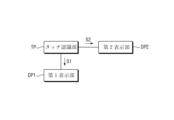
図1は一実施形態によるボタン複合構造物のブロック図である。 FIG. 1 is a block diagram of a button composite structure according to one embodiment.
図1を参照すると、一実施形態によるボタン複合構造物はタッチ認識部TP、第1表示部DP1、および第2表示部DP2を含む。 Referring to FIG. 1, a button composite structure according to one embodiment includes a touch recognition part TP, a first display part DP1 and a second display part DP2.
タッチ認識部TPはタッチ入力を認識する役割をする。例えば、タッチ認識部TPはボタン複合構造物にタッチ入力になると、タッチ入力信号S1,S2を生成する。 The touch recognition part TP plays a role of recognizing a touch input. For example, the touch recognizer TP generates touch input signals S1 and S2 when a touch input is applied to the button composite structure.
第1表示部DP1は画像を表示する表示パネルを含む。表示パネルとしては液晶表示パネルを適用することができる。以下の実施形態では表示パネルとして液晶表示パネルを例として説明するが、表示パネルはこれに制限されるものではなく、電気泳動表示パネル、有機発光表示パネル、マイクロLED表示パネル、プラズマ表示パネル、電界放出表示パネル、陰極線表示パネルなどにも適用することができる。 The first display part DP1 includes a display panel that displays an image. A liquid crystal display panel can be applied as the display panel. In the following embodiments, a liquid crystal display panel will be described as an example of a display panel, but the display panel is not limited to this, and includes an electrophoretic display panel, an organic light emitting display panel, a micro LED display panel, a plasma display panel, an electric field display panel, and a display panel. It can also be applied to emissive display panels, cathode ray display panels, and the like.
第1表示部DP1はタッチ認識部TPと電気的に接続される。第1表示部DP1はタッチ認識部TPで生成されたタッチ入力信号S1の提供を受けてタッチ入力信号S1に対応する画面を表示する。 The first display part DP1 is electrically connected to the touch recognition part TP. The first display part DP1 receives the touch input signal S1 generated by the touch recognition part TP and displays a screen corresponding to the touch input signal S1.
第2表示部DP2は発光する発光素子を含む。前記発光素子の例としてはLEDが挙げられる。すなわち、第2表示部DP2はLED発光素子を含むことができる。ただし、これに制限されず、第2表示部DP2はハロゲンランプ、白熱電球、または三波長などを含むことができる。 The second display part DP2 includes light emitting elements that emit light. An LED is mentioned as an example of the said light emitting element. That is, the second display part DP2 may include an LED light emitting element. However, without being limited thereto, the second display part DP2 may include a halogen lamp, an incandescent lamp, or three wavelengths.
第2表示部DP2はタッチ認識部TPと電気的に接続される。第2表示部DP2はタッチ認識部TPで生成されたタッチ入力信号S2の提供を受けてタッチ入力信号S2に対応して光を発光する。 The second display part DP2 is electrically connected to the touch recognition part TP. The second display part DP2 receives the touch input signal S2 generated by the touch recognition part TP and emits light corresponding to the touch input signal S2.
いくつかの実施形態で第2表示部DP2はタッチ認識部TPで生成されたタッチ入力信号S2と関係がなく光を発光することもできる。 In some embodiments, the second display part DP2 may emit light regardless of the touch input signal S2 generated by the touch recognition part TP.
以下、一実施形態によるボタン複合構造物のより具体的な構造について説明する。 Hereinafter, a more specific structure of the button composite structure according to one embodiment will be described.
図1で上述したボタン複合構造物の各構成の図面符号は説明の便宜上付けられたものであり、以下で説明するボタン複合構造物の各構成の図面符号と異なってもよい。 The reference numerals of each component of the button composite structure described above in FIG. 1 are attached for convenience of explanation, and may be different from the reference numerals of each component of the button composite structure described below.
図2は一実施形態によるボタン複合構造物の断面図である。 FIG. 2 is a cross-sectional view of a button composite structure according to one embodiment.
図2を参照すると、一実施形態によるボタン複合構造物1は表示パネル10、部材20、およびボタン構造物30を含む。
Referring to FIG. 2, a
表示パネル10は図1で上述した第1表示部DP1と同じ構造を含むことができる。
The
表示パネル10は第1基板11、第1基板11に対向する第2基板12および第1基板11と第2基板12の間に介在する液晶層13を含む。第1基板11と第2基板12の縁にはシーリング部材14が配置され、第1基板11と第2基板12を結合し、液晶層13の液晶分子が外部に流出することを防止することができる。
The
第1基板11と第2基板12のいずれか一つは薄膜トランジスタ基板であり、他の一つはカラーフィルタ基板であり得る。本実施形態では第1基板11が薄膜トランジスタ基板であり、第2基板12がカラーフィルタ基板である場合を例示する。表示方向は第2基板12の上面外側方向になる。第2基板12は第1基板11より表示方向を基準として上部に配置される。したがって、第2基板12は上部基板であり得、第1基板11は下部基板であり得る。
One of the
第1基板11と第2基板12はそれぞれガラス、石英などからなる絶縁基板およびその上に配置された配線、金属、半導体層、絶縁膜、カラーフィルタ、ブラックマトリクスなどの構造物を含むことができる。前記構造物はそれぞれ第1基板11の絶縁基板と第2基板12の絶縁基板の互いに対向する一面上に配置される。図面では便宜上絶縁基板上に配置される構造物の図示は省略し、第1基板11と第2基板12の絶縁基板の形状のみを示した。以下では、第1基板11または第2基板12の背面形状を言及する際、該当形状は第1基板11の絶縁基板の背面形状または第2基板12の絶縁基板の背面形状を意味するものであり得る。
Each of the
表示パネル10上には表示パネル10に付着した部材20が配置される。
A
部材20は第3基板21、およびタッチ層TSLを含む。タッチ層TSLは第3基板21上に配置される。タッチ層TSLは第3基板21と第2基板12の間に配置される。
タッチ層TSLと第2基板12の間には第1結合部材AM1が配置される。第1結合部材AM1によりタッチ層TSLと第2基板12が相互結合される。第1結合部材AM1は両面テープであり得るが、これに制限されず、通常の結合部材を適用することもできる。
A first coupling member AM1 is disposed between the touch layer TSL and the
第1結合部材AM1はタッチ層TSLと第2基板12の間の両端部に配置される。すなわち、第1結合部材AM1が配置されていない中央部でタッチ層TSLと第2基板12の間には離隔空間が配置される。前記離隔空間によりタッチ層TSLと第2基板12は離隔して配置されることができる。
A first coupling member AM1 is disposed at both ends between the touch layer TSL and the
第3基板21はガラス、または石英などからなる絶縁基板であり得る。第3基板21は第1基板11と同じ物質を含むことができる。第3基板21の平面上の大きさは第2基板12の平面上の大きさと同一であり得るが、これに制限されるものではない。
The
タッチ層TSLは第3基板21の第2基板12に向かう一面上に配置される。
The touch layer TSL is disposed on one side of the
タッチ層TSLは複数のタッチ電極、および前記複数のタッチ電極を覆うタッチ絶縁層を含むことができる。前記タッチ電極は導電物質を含むことができ、前記タッチ絶縁層は無機物質、または有機物質を含むことができる。 The touch layer TSL may include a plurality of touch electrodes and a touch insulating layer covering the plurality of touch electrodes. The touch electrode may include a conductive material, and the touch insulating layer may include an inorganic material or an organic material.
第3基板21の一面上に複数のタッチ電極が配置され、前記複数のタッチ電極上に前記タッチ絶縁層が前記複数のタッチ電極を覆って配置される。
A plurality of touch electrodes are disposed on one surface of the
前記タッチ絶縁層は第1結合部材AM1と直接接し得る。前記タッチ絶縁層は第1結合部材AM1により第2基板12に付着することができる。
The touch insulation layer may be in direct contact with the first coupling member AM1. The touch insulating layer may be attached to the
タッチ層TSLは第3基板21の一面の反対面である他面上に印加されたタッチ入力信号を感知する。タッチ層TSLは静電容量方式でタッチ入力地点の座標を取得する。前記静電容量方式は自己静電容量(self capacitance)方式または相互静電容量(mutual capacitance)方式でタッチされた地点の座標情報を取得することができる。
The touch layer TSL senses a touch input signal applied to the opposite surface of the
部材20上にはボタン構造物30が配置される。ボタン構造物30は第3基板21の他面上に配置される。すなわち、ボタン構造物30と前記タッチ絶縁層の間にはタッチ層TSLが配置され、ボタン構造物30と表示パネル10の間には部材20が配置されることができる。
A
ボタン構造物30はボタン本体部40、ボタン装着部50、発光部60、およびボタン部70を含む。
The
ボタン構造物30と第3基板21の間には第2結合部材AM2が配置される。第2結合部材AM2は粘着剤であり得るが、これに制限されるものではない。
A second coupling member AM2 is arranged between the
ボタン本体部40は第2結合部材AM2と直接接し得る。ボタン本体部40は第2結合部材AM2により第3基板21の他面上に直接付着して固定される。
The
ボタン装着部50はボタン本体部40と締結され、ボタン部70はボタン装着部50と連結される。
The
図面に示していないが、部材20と表示パネル10の間には回路基板(図4の「CB」を参照)がさらに配置されることができる。発光部60は発光素子、および焦点可変部を含む。部材20と表示パネル10の間に配置された回路基板CB上には発光素子が配置される。焦点可変部はボタン本体部40内に配置される。
Although not shown in the drawings, a circuit board (see “CB” in FIG. 4) may be further arranged between the
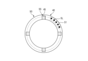
図3は一実施形態によるボタン複合構造物の平面図である。 FIG. 3 is a plan view of a button composite structure according to one embodiment.
図3を参照すると、ボタン装着部50、および発光部60の平面形状は円形の開口を含むリング形状を含む。ボタン部70の平面形状は円形を含む。ただし、これに制限されず、ボタン装着部50、および発光部60の平面形状は中心部に開口を含んで前記開口を囲む形状であれば制限はない。また、ボタン部70の平面形状はこれに制限されず、長方形、正方形、楕円形、またはその他多角形を含むことができる。
Referring to FIG. 3, the planar shape of the
例示した実施形態でボタン装着部50の前記開口の形状とボタン部70の平面形状は同一であり得る。ただし、これに制限されず、ボタン装着部50の前記開口の形状とボタン部70の平面形状は互いに異なってもよい。
In the illustrated embodiment, the shape of the opening of the
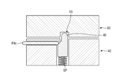
図4は一実施形態によるボタン複合構造物の断面図である。図5はボタン部に入力が印加されるときのボタン複合構造物の断面図である。 FIG. 4 is a cross-sectional view of a button composite structure according to one embodiment. FIG. 5 is a cross-sectional view of the button composite structure when an input is applied to the button portion.
図4および図5を参照すると、ボタン本体部40はこれに制限されるものではないが、下側ラインをなす第1部分、および前記第1部分から突出した第2部分に区分される。ボタン本体部40の第1部分にはロックピン45が配置される。ロックピン45はボタン本体部40の前記第1部分から厚さ方向に突出し得る。
4 and 5, the
ボタン本体部40上にはボタン装着部50が配置される。ボタン装着部50はボタン本体部40の前記第1部分の上部、および前記第2部分の左側上に配置される。
A
ボタン本体部40の下面にはロック溝55が配置される。ロック溝55はボタン本体部40の下面から上部方向に湾入した形状を含む。
A
ボタン装着部50はロック溝55にロックピン45が挿入される方式でボタン本体部40とロック/アンロック(Lock/Unlock)の関係を有することができる。すなわち、ロック溝55にロックピン45が挿入されるとボタン装着部50はボタン本体部40と締結関係(ロック状態)を有することができ、ロック溝55からロックピン45が抜けるとボタン装着部50はボタン本体部40と分離関係(アンロック状態)を有することができる。
The
ロック溝55とロックピン45の挿入/抜きの関係については図6ないし図10を参照して後述する。
The relationship between the
一実施形態で部材20と表示パネル10の間には回路基板CBが配置される。回路基板CB上には発光部60を構成する発光素子が実装する。発光部60は図1で上述した第2表示部DP2と同じ構成であり得る。
A circuit board CB is arranged between the
発光素子61の例としてはLEDが挙げられる。すなわち、発光素子61はLED発光素子を含むことができる。ただし、これに制限されず、発光素子61はハロゲンランプ、白熱電球、または三波長などを含むことができる。 An example of the light emitting element 61 is an LED. That is, light emitting element 61 may include an LED light emitting element. However, the light emitting device 61 is not limited to this, and may include a halogen lamp, an incandescent lamp, or three wavelengths.
回路基板51の一側(図面上右側端部)には信号配線SLが連結される。信号配線SLは回路基板51の一側(図面上右側端部)に連結されて図面上の右側方向に延びて第1結合部材AM1を貫通して延び得る。信号配線SLは表示パネル10と電気的に接続される。
A signal line SL is connected to one side of the circuit board 51 (the right end in the drawing). The signal line SL may be connected to one side (the right end in the drawing) of the
ボタン装着部50はボタン部70と対向する部分の一部がボタン部70から遠くなる方向に湾入した湾入パターンIDPを含む。すなわち、湾入パターンIDPはボタン装着部50のボタン部70と対向する側面から図面上の右側方向に湾入した形状を含むことができる。
The
ボタン装着部50の湾入パターンIDPによりボタン装着部50はコの字の断面形状を含む。コの字の断面形状のうち下辺(またはライン)上にはダンパDMがさらに配置されることができる。f
ボタン部70はボタン装着部50の側面上に配置されてボタン装着部50のダンパDM上に配置される。ボタン部70はボタン装着部50の湾入パターンIDPに向かって突出した突出パターンPTを含む。突出パターンPTは、すなわち、図面上の右側方向に向かって突出した形状を含むことができる。
The
The
突出パターンPTとボタン装着部50のコの字の断面形状の下辺の間にはダンパDMが配置される。ダンパDMは突出パターンPTおよびボタン装着部50のコの字の断面形状の下辺とそれぞれ直接接し得る。
A damper DM is arranged between the protruding pattern PT and the lower side of the U-shaped cross-sectional shape of the
ボタン部70は透明な物質を含むことができる。
発光素子と重畳配置されたボタン装着部50の上部方向の表面上には焦点可変部65がさらに配置される。
A focus
焦点可変部65は発光素子61と厚さ方向で重畳配置される。
The
焦点可変部65は発光素子61から発光した光の焦点を可変的に制御する役割をする。例えば、焦点可変部65は光学レンズを含むことができる。
The focus
ボタン部70は透明導電物質を含む。前記透明導電物質の例としては、インジウムスズ酸化物(Indium Tin Oxide,ITO)、IZO(Indium Zinc Oxide)、AZO(Antimony Zinc Oxide)、ITZO(Indium Tin Zinc Oxide)、ZnO(Zinc Oxide)、およびSnO2(Tin Oxide)、カーボンナノチューブ(Carbon Nano Tube)、グラフェン(graphene)、伝導性高分子(例示的にPEDOT)、および銀ナノワイヤ(AgNW)などが挙げられる。
一実施形態でボタン部70は表面に上記した透明導電物質がコートされて形成されることができる。上記した透明導電物質はボタン部70の表面全体にコートされる。
In one embodiment, the
前記透明導電物質がコートされたボタン部70と部材20(第3基板21)の間には導電性テープCMがさらに配置される。例えば、前記透明導電物質がコートされたボタン部70の下側部(下面)と部材20(第3基板21)の間には導電性テープCMが配置される。導電性テープCMはボタン部70の下側部(下面)に付着する。
A conductive tape CM is further disposed between the
導電性テープCMは弾性がある物質であり、かつ導電性を有する物質を含むことができる。 The conductive tape CM is an elastic material and can include a material having conductivity.
ボタン部70に物理的圧力が印加されないと導電性テープCMは図4のように部材20(第3基板21)と厚さ方向に離隔して配置され、ボタン部70に所定の物理的圧力が印加されると導電性テープCMは図5に示すように部材20(第3基板21)に直接接し得る。いくつかの実施形態でボタン部70に所定の物理的圧力が印加されても導電性テープCMは図5に示すように部材20(第3基板21)に直接接しなくてもい。
When no physical pressure is applied to the
以下、ボタン複合構造物1の動作についてより具体的に説明する。
The operation of the button
ボタン部70を介して物理的タッチ信号が入力される。前記物理的タッチ信号は物理的圧力であり得る。以下、物理的タッチ信号を入力信号という。
A physical touch signal is input through the
透明導電物質を含むボタン部70を介して入力信号が印加されるとボタン部70は図面上の下部方向(厚さ方向)に移動し、これによりボタン部70の下面上の導電性テープCMは部材20(第3基板21)に接するようになる。前述したようにボタン部70が図面上の下部方向(厚さ方向)に移動してもボタン部70の下面上の導電性テープCMは部材20(第3基板21)に接しない。ただし、この場合にもボタン部70を介して入力信号が印加されていない場合より導電性テープCMと部材20間の離隔距離が小さくなる。
When an input signal is applied through the
表示パネル10と電気的に接続された外部装置は部材20のタッチ層TSLと導電性を有するボタン部70、およびそれに付着した導電性テープCMの離隔距離(具体的には導電性テープCMとタッチ層TSLの離隔距離)によりボタン部70への入力信号印加の有無、および前記入力信号の強度を判断することができる。
An external device electrically connected to the
例えば、図4のようにボタン部70に入力信号が印加されていない場合、前記外部装置は部材20のタッチ層TSLと導電性を有するボタン部70、およびそれに付着した導電性テープCMは相互離隔したまま存在してボタン部70に入力信号が印加されていないものと認識し、図5のようにボタン部70に入力信号が印加された場合、前記外部装置は部材20のタッチ層TSLと導電性を有するボタン部70、およびそれに付着した導電性テープCMが相互接してボタン部70に入力信号が印加されたものと認識することができる。前述したように前記外部装置はボタン部70に入力信号が印加され、導電性テープCMが部材20に接しなくても導電性テープCMと部材20の間の離隔距離が所定の離隔距離以下になると、ボタン部70に入力信号が印加されたものと認識することができる。
For example, when no input signal is applied to the
前記外部装置は上述した方式でボタン部70に入力信号が印加されたことを認識すると、表示パネル10が特定画面を出射するように表示パネル10を制御することができる。
When the external device recognizes that the input signal is applied to the
突出パターンPTとボタン装着部50のコの字の断面形状の下辺の間にはダンパDMが配置される。ダンパDMは突出パターンPTおよびボタン装着部50のコの字の断面形状の下辺とそれぞれ直接接し得る。ダンパDMはフレキシブルな物質を含むことができる。例えば、ダンパDMは収縮と延伸が相対的に自由な弾性物質を含むことができる。
A damper DM is arranged between the protruding pattern PT and the lower side of the U-shaped cross-sectional shape of the
ダンパDMが配置されていない場合のボタン部70は、入力信号が印加されてもボタン部70の突出パターンPTがボタン装着部50のコの字状の下辺と干渉されるので、下部方向(厚さ方向)に移動しない。ただし、一実施形態によるボタン複合構造物1は、突出パターンPTとボタン装着部50のコの字の断面形状の下辺の間にはフレキシブルなダンパDMが配置されることによって、ボタン部70に入力信号が印加されるときボタン部70の突出パターンPTがボタン装着部50のコの字状の下辺と干渉されて下部方向(厚さ方向)に移動しないことを防止するだけでなく、入力信号がこれ以上印加されないとき再び、ボタン部70が上部方向(厚さ方向)に移動することを容易にすることができる。
In the case where the damper DM is not arranged, the projecting pattern PT of the
複数の信号配線SLは第1信号配線、および第2信号配線を含む。発光素子61は信号配線SLのうち第1信号配線を介して電源の供給を受けるように構成される。すなわち、前記第1信号配線を介して発光素子61に電源が供給されることができる。 The plurality of signal lines SL includes first signal lines and second signal lines. The light emitting element 61 is configured to receive power supply through the first signal wiring line among the signal wiring lines SL. That is, power can be supplied to the light emitting device 61 through the first signal wiring.
発光素子61はボタン部70に入力された入力信号に応じて発光するように構成される。この場合、複数の信号配線SLのうち第2信号配線はボタン部70に入力された入力信号をメイン制御部に送出し、前記メイン制御部から発光素子61の発光イベントを制御する信号を回路基板51の発光素子61に提供する役割をする。第2信号配線は表示パネル10と電気的に接続された前記外部装置と電気的に接続される。
The light emitting element 61 is configured to emit light according to an input signal input to the
図6は一実施形態によるボタン本体部、およびボタン回路部を示す平面図である。図7は一実施形態によるボタン本体部とボタン回路部が締結された状態を示す平面図である。図8は一実施形態によるボタン本体部とボタン回路部が分解された状態を示す平面図である。図9は一実施形態によるボタン本体部とボタン回路部が締結された状態を示す断面図である。図10は一実施形態によるボタン本体部とボタン回路部が分解された状態を示す断面図である。 FIG. 6 is a plan view showing a button main body and a button circuit according to one embodiment. FIG. 7 is a plan view showing a state in which the button main body and the button circuit are fastened according to one embodiment. FIG. 8 is a plan view showing a disassembled state of the button main body and the button circuit according to one embodiment. FIG. 9 is a cross-sectional view showing a state in which a button body and a button circuit are coupled according to one embodiment. FIG. 10 is a cross-sectional view showing a disassembled state of the button main body and the button circuit according to one embodiment.
まず、図6を参照すると、ボタン本体部40のロックピン45は複数であり得る。図面に例示したロックピン45の配置はこれに制限されるものではない。
First, referring to FIG. 6, the
ボタン装着部50のロック溝55は複数であり得る。一実施形態でロック溝55の個数はロックピン45の個数と同一であり得る。
A plurality of locking
図7を参照すると、複数のロックピン45と複数のロック溝55が互いに厚さ方向で重なる。
Referring to FIG. 7, a plurality of locking
ボタン本体部40の表面から厚さ方向に突出したロックピン45はボタン本体部40の下面から上部方向に湾入したロック溝55に挿入される。複数のロックピン45はそれぞれ厚さ方向に対応するロック溝55に挿入される。
A
このようにロック溝55は、ボタン装着部50のロック溝55にロックピン45が挿入される方式でボタン本体部40とロック/アンロック(Lock/Unlock)の関係を有することができる。
As such, the
ロックピン45はロック溝55に挿入される挿入部、挿入部の下側部と連結されたボディ部、および前記ボディ部の下側部と連結された弾性部SPを含む。断面上、挿入部の幅はボディ部、および弾性部SPの幅よりそれぞれ小さくてもよい。ボディ部の前記挿入部から一側に突出した部分は断面上傾いた形状を有することができる。
The
図8を参照すると、図7の実施形態のようにボタン本体部40と締結されたボタン装着部50を時計回り(図面に例示した)または反時計回りに回転させてボタン本体部40からボタン装着部50を分離させることができる。ただし、ロック溝55に挿入されたロックピン45によりボタン装着部50を回転させてもロック溝55からロックピン45を容易に抜くことができない。
Referring to FIG. 8, the
図9、および図10を参照すると、ロック解除ピンPINによりロック溝55からロックピン45を抜く方式でボタン装着部50をボタン本体部40から分離させることができる。
9 and 10, the
すなわち、ロック解除ピンPINはロックピン45の前記ボディ部の前記挿入部から一側に突出して傾いた部分を前記一側の反対である他側方向に押してロックピン45の前記挿入部をロック溝55から抜くことができる。
That is, the unlocking pin PIN pushes the inclined portion protruding from the insertion portion of the body portion of the
一実施形態によるロックピン45は前述したように前記ボディ部の下側部と連結された弾性部SPをさらに含むが、弾性部SPはばねを含むことができる。弾性部SPはロック解除ピンPINによりロックピン45の前記ボディ部の前記挿入部から一側に突出して傾いた部分を前記一側の反対である他側方向に押すときロックピン45が下側方向に容易に動くようにして前記挿入部をロック溝55から容易に抜くようにする役割をすることができる。
The
一実施形態による互いに対応するロック溝55およびロックピン45は複数であるから複数のロックピン45を同時に下側方向に移動させる場合にのみボタン本体部40とボタン装着部50の完全な分離がなされる。
Since there are a plurality of
すなわち、複数のロック解除ピンPINによって同時に複数のロック溝55からそれぞれ対応する複数のロックピン45を抜く方式でボタン装着部50をボタン本体部40から完全に分離させることができる。
That is, the
図10に示すように前記挿入部がロック溝55から抜けると図8で前述したようにボタン本体部40と締結されたボタン装着部50を時計回り(図面に例示した)または反時計回りに回転させてボタン本体部40からボタン装着部50を分離させることができる。
As shown in FIG. 10, when the insertion part is pulled out of the
ボタン構造物が第3基板を貫通して第3基板下部のデッキに締結される場合、ボタン構造物をデッキに締結するために第3基板に貫通孔を開ける過程で第3基板の破損が生じ得るだけでなく、コストの消耗も少なくなく、デザイン自由度が大きく落ち得る。 When the button structure penetrates the third substrate and is fastened to the deck under the third substrate, the third substrate may be damaged during the process of drilling a through hole in the third substrate to fasten the button structure to the deck. Not only does this increase the cost, but it also consumes a considerable amount of cost, and the degree of freedom in design can be greatly reduced.
しかし、一実施形態によるボタン複合構造物1によれば、第3基板21の貫通孔を形成することなく第3基板21に直接ボタン構造物30が積層されることによって、第3基板21の破損発生を減らし、コストを減らして、デザイン自由度を高めることができる。
However, according to the button
また、第3基板の貫通孔を介してボタン構造物を第3基板の下部のデッキに締結する場合、第3基板の貫通孔による漏水によってボタン構造物だけでなく、表示パネルの不良が発生する場合もある。 In addition, when the button structure is fastened to the lower deck of the third substrate through the through-hole of the third substrate, water leakage through the through-hole of the third substrate may cause defects in the button structure as well as the display panel. In some cases.
しかし、一実施形態によるボタン複合構造物1の場合、第3基板21に貫通孔を形成しないため、漏水による表示パネル10、およびボタン構造物30の故障を減らすことができる。
However, in the case of the button
さらに、ボタン構造物はボタン入力信号を収容する回路部をさらに含むが、回路部が故障する場合、ボタン構造物がデッキに締結されて分離されにくい構造であると、第3基板を分解し故障したボタン構造物をデッキから分離しなければならない。この場合、第3基板の分解作業が容易ではなく、ボタン構造物の修理に多くの時間が必要とされる。 In addition, the button structure further includes a circuit unit for receiving button input signals. button structure must be separated from the deck. In this case, it is not easy to disassemble the third substrate, and it takes a long time to repair the button structure.
しかし、一実施形態によるボタン複合構造物1によれば、回路基板51を含む回路部を含まないボタン本体部40を第3基板21に固定させて回路部を含むボタン装着部50をボタン本体部40とロック/アンロックするようにすることによって、回路部が故障する場合、ボタン装着部50のみを容易に交換することができ、ボタン構造物の修理が短期間で行われることができる。
However, according to the button
さらに、一実施形態によるボタン複合構造物1の互いに対応するロック溝55およびロックピン45は複数で構成されることで、複数のロック解除ピンPINによって同時に複数のロック溝55からそれぞれ対応する複数のロックピン45を抜く方式でボタン装着部50をボタン本体部40から完全に分離させなければならないので、ボタン本体部40およびボタン部70の盗難防止を容易にすることができる。
In addition, since the button
さらに、一実施形態によるボタン複合構造物1はボタン部70が透明導電物質を含み、部材20のタッチ層TSLと静電気的方式で動作するので、ボタン部70の入力信号を収容するボタンスイッチ、およびボタンスイッチが実装した回路基板を省略することができ、ボタン複合構造物1の構成を単純化することができる。
Further, the button
以上、添付する図面を参照して本発明の実施形態について説明したが、本発明が属する技術分野で通常の知識を有する者は、本発明のその技術的思想や必須の特徴を変更せず、他の具体的な形態で実施できることを理解することができる。したがって、上記一実施形態はすべての面で例示的なものであり、限定的なものではないと理解しなければならない。 Although the embodiments of the present invention have been described above with reference to the accompanying drawings, those who have ordinary knowledge in the technical field to which the present invention belongs may not change the technical idea or essential features of the present invention, It can be understood that it can be embodied in other specific forms. Therefore, it should be understood that the above-described embodiment is illustrative in all respects and not restrictive.
Claims (12)
前記第2基板上の部材と、
前記表示パネルと前記部材の一面を結合する第1結合部材と、
前記部材の一面の反対面である他面上に配置されたボタン構造物と、
前記部材の他面と前記ボタン構造物を結合する第2結合部材を含み、
前記部材は第3基板、および前記第3基板上のタッチ層を含み、
前記タッチ層は前記部材の前記一面を含み、
前記タッチ層は前記第1結合部材によって前記表示パネルと結合され、
前記ボタン構造物は前記第2結合部材によって前記第3基板と直接結合され、
前記ボタン構造物は透明導電物質を含む、ボタン複合構造物。 a display panel comprising a first substrate, a second substrate over the first substrate, and a liquid crystal layer between the first substrate and the second substrate;
a member on the second substrate;
a first coupling member that couples the display panel and one surface of the member;
a button structure disposed on the other surface opposite to the one surface of the member;
a second connecting member that connects the other surface of the member and the button structure;
the member includes a third substrate and a touch layer on the third substrate;
the touch layer includes the one surface of the member;
the touch layer is coupled with the display panel by the first coupling member;
the button structure is directly coupled to the third substrate by the second coupling member;
A button composite structure, wherein the button structure comprises a transparent conductive material.
前記ボタン部は前記透明導電物質を含む、請求項1に記載のボタン複合構造物。 The button structure includes a button body fixed to the third substrate, a button mounting part fastened to the button body, and a button part connected to the button mounting part,
2. The button composite structure of claim 1, wherein said button portion comprises said transparent conductive material.
前記ボタン装着部はロック溝を含み、
前記ボタン装着部は前記ロック溝に前記ロックピンが挿入される方式で前記ボタン本体部に締結されるように構成された、請求項2に記載のボタン複合構造物。 the button body includes a lock pin;
the button mounting portion includes a lock groove,
The button composite structure according to claim 2, wherein the button mounting part is configured to be fastened to the button body part by inserting the lock pin into the lock groove.
複数の前記ロックピンはそれぞれ複数のロック解除ピンによって同時に前記ロック溝から抜く方式で前記ボタン本体部と分離されるように構成された、請求項3に記載のボタン複合構造物。 said lock pin is plural,
4. The button composite structure according to claim 3, wherein the plurality of lock pins are configured to be separated from the button main body by a plurality of lock release pins, respectively, in a manner of pulling out from the lock groove at the same time.
前記ボタン部に物理的入力が印加されないと前記導電テープは前記第3基板から離隔する、請求項5に記載のボタン複合構造物。 when a physical input is applied to the button portion, the conductive tape is in contact with the third substrate;
6. The button composite structure of claim 5, wherein the conductive tape separates from the third substrate when no physical input is applied to the button portion.
前記ボタン部は前記湾入部に向かって突出した突出部を含み、前記湾入部と前記突出部の間に配置されたダンパをさらに含む、請求項6に記載のボタン複合構造物。 The button mounting portion includes a recessed portion recessed in a direction away from the button portion,
7. The button composite structure of claim 6, wherein the button portion includes a protrusion projecting toward the recessed portion, and further including a damper disposed between the recessed portion and the protrusion.
前記回路基板上に実装した発光素子がさらに配置された、請求項2に記載のボタン複合構造物。 further comprising a circuit board disposed between the member and the display panel;
3. The button composite structure of claim 2, further comprising a light emitting device mounted on the circuit board.
前記発光素子は前記信号配線を介して電源の供給を受けるように構成された、請求項8に記載のボタン複合構造物。 further comprising signal wiring electrically connected to the circuit board;
9. The button composite structure of claim 8, wherein the light emitting element is configured to receive power through the signal wiring.
Applications Claiming Priority (3)
| Application Number | Priority Date | Filing Date | Title |
|---|---|---|---|
| KR10-2020-0021259 | 2020-02-20 | ||
| KR1020200021259A KR102293639B1 (en) | 2020-02-20 | 2020-02-20 | Button complex structure |
| PCT/KR2021/000361 WO2021167246A1 (en) | 2020-02-20 | 2021-01-12 | Button composite structure |
Publications (2)
| Publication Number | Publication Date |
|---|---|
| JP2023513195A true JP2023513195A (en) | 2023-03-30 |
| JP7397209B2 JP7397209B2 (en) | 2023-12-12 |
Family
ID=77391038
Family Applications (1)
| Application Number | Title | Priority Date | Filing Date |
|---|---|---|---|
| JP2022547905A Active JP7397209B2 (en) | 2020-02-20 | 2021-01-12 | button composite structure |
Country Status (6)
| Country | Link |
|---|---|
| US (1) | US12106912B2 (en) |
| EP (1) | EP4109482A4 (en) |
| JP (1) | JP7397209B2 (en) |
| KR (1) | KR102293639B1 (en) |
| AU (1) | AU2021222059C1 (en) |
| WO (1) | WO2021167246A1 (en) |
Families Citing this family (1)
| Publication number | Priority date | Publication date | Assignee | Title |
|---|---|---|---|---|
| JP7416235B2 (en) * | 2020-05-28 | 2024-01-17 | オムロン株式会社 | Push button switches, operating units, and gaming machines |
Citations (4)
| Publication number | Priority date | Publication date | Assignee | Title |
|---|---|---|---|---|
| JP2012129171A (en) * | 2010-12-17 | 2012-07-05 | Gunze Ltd | Touch switch |
| JP2016061878A (en) * | 2014-09-17 | 2016-04-25 | 凸版印刷株式会社 | Liquid crystal display panel |
| KR20180080151A (en) * | 2018-06-21 | 2018-07-11 | 안송길 | Physicl key for removable and terminal using the same |
| US20190272053A1 (en) * | 2018-03-05 | 2019-09-05 | Advanced Silicon Sa | Transparent button for capacitive touch screen |
Family Cites Families (11)
| Publication number | Priority date | Publication date | Assignee | Title |
|---|---|---|---|---|
| JPH0729726A (en) | 1993-07-15 | 1995-01-31 | Hitachi Metals Ltd | Manufacture of magnet roll |
| JPH0729726U (en) * | 1993-10-28 | 1995-06-02 | 日本航空電子工業株式会社 | Panel switch |
| KR100718988B1 (en) * | 2005-07-27 | 2007-05-16 | (주)멜파스 | Input device of electronic device |
| KR100995056B1 (en) * | 2008-08-27 | 2010-11-18 | 주식회사 토비스 | LCD display module and terminal equipped with the same |
| KR101893922B1 (en) * | 2011-09-02 | 2018-08-31 | 삼성전자 주식회사 | User terminal and display apparatus thereof |
| US8723824B2 (en) * | 2011-09-27 | 2014-05-13 | Apple Inc. | Electronic devices with sidewall displays |
| JPWO2014006756A1 (en) * | 2012-07-06 | 2016-06-02 | 富士通株式会社 | Switch unit and electronic device |
| US9519349B2 (en) * | 2014-10-30 | 2016-12-13 | Industrial Smoke & Mirrors, Inc. | Touch screen interface device |
| EP3287875B1 (en) * | 2015-04-23 | 2019-11-13 | Alps Alpine Co., Ltd. | Input assistance device and input system |
| KR102277114B1 (en) * | 2020-01-03 | 2021-07-14 | 주식회사 토비스 | Button complex structure |
| KR102288129B1 (en) * | 2020-02-06 | 2021-08-10 | 주식회사 토비스 | Button complex structure |
-
2020
- 2020-02-20 KR KR1020200021259A patent/KR102293639B1/en active Active
-
2021
- 2021-01-12 EP EP21757360.9A patent/EP4109482A4/en active Pending
- 2021-01-12 AU AU2021222059A patent/AU2021222059C1/en active Active
- 2021-01-12 JP JP2022547905A patent/JP7397209B2/en active Active
- 2021-01-12 WO PCT/KR2021/000361 patent/WO2021167246A1/en not_active Ceased
- 2021-01-12 US US17/796,268 patent/US12106912B2/en active Active
Patent Citations (4)
| Publication number | Priority date | Publication date | Assignee | Title |
|---|---|---|---|---|
| JP2012129171A (en) * | 2010-12-17 | 2012-07-05 | Gunze Ltd | Touch switch |
| JP2016061878A (en) * | 2014-09-17 | 2016-04-25 | 凸版印刷株式会社 | Liquid crystal display panel |
| US20190272053A1 (en) * | 2018-03-05 | 2019-09-05 | Advanced Silicon Sa | Transparent button for capacitive touch screen |
| KR20180080151A (en) * | 2018-06-21 | 2018-07-11 | 안송길 | Physicl key for removable and terminal using the same |
Also Published As
| Publication number | Publication date |
|---|---|
| US12106912B2 (en) | 2024-10-01 |
| AU2021222059C1 (en) | 2023-12-14 |
| AU2021222059A1 (en) | 2022-09-29 |
| EP4109482A4 (en) | 2024-05-01 |
| EP4109482A1 (en) | 2022-12-28 |
| WO2021167246A1 (en) | 2021-08-26 |
| KR102293639B1 (en) | 2021-08-26 |
| AU2021222059B2 (en) | 2023-09-07 |
| US20230077786A1 (en) | 2023-03-16 |
| JP7397209B2 (en) | 2023-12-12 |
Similar Documents
| Publication | Publication Date | Title |
|---|---|---|
| US11500496B2 (en) | Display device | |
| EP3333682B1 (en) | Electronic device | |
| JP7336603B2 (en) | button composite structure | |
| TWI740959B (en) | Display apparatus | |
| CN107680984A (en) | Organic Light Emitting Display Module | |
| CN112992988A (en) | Display device | |
| TWI489338B (en) | Polarization structure with touch function | |
| AU2020418324B2 (en) | Button composite structure | |
| JP7397209B2 (en) | button composite structure | |
| CN113130584A (en) | Display device | |
| KR20160037469A (en) | Touch window and touch device | |
| US20200241677A1 (en) | Polarized light touch device, method for manufacturing same and flexible display device | |
| KR102187949B1 (en) | Touch window | |
| KR20220110148A (en) | Display device |
Legal Events
| Date | Code | Title | Description |
|---|---|---|---|
| A621 | Written request for application examination |
Free format text: JAPANESE INTERMEDIATE CODE: A621 Effective date: 20220805 |
|
| A977 | Report on retrieval |
Free format text: JAPANESE INTERMEDIATE CODE: A971007 Effective date: 20230721 |
|
| A131 | Notification of reasons for refusal |
Free format text: JAPANESE INTERMEDIATE CODE: A131 Effective date: 20230815 |
|
| A521 | Request for written amendment filed |
Free format text: JAPANESE INTERMEDIATE CODE: A523 Effective date: 20231106 |
|
| TRDD | Decision of grant or rejection written | ||
| A01 | Written decision to grant a patent or to grant a registration (utility model) |
Free format text: JAPANESE INTERMEDIATE CODE: A01 Effective date: 20231121 |
|
| A61 | First payment of annual fees (during grant procedure) |
Free format text: JAPANESE INTERMEDIATE CODE: A61 Effective date: 20231130 |
|
| R150 | Certificate of patent or registration of utility model |
Ref document number: 7397209 Country of ref document: JP Free format text: JAPANESE INTERMEDIATE CODE: R150 |