JP2023150049A - Energy storage element - Google Patents

Energy storage element Download PDF

Info

Publication number
JP2023150049A
JP2023150049A JP2022058933A JP2022058933A JP2023150049A JP 2023150049 A JP2023150049 A JP 2023150049A JP 2022058933 A JP2022058933 A JP 2022058933A JP 2022058933 A JP2022058933 A JP 2022058933A JP 2023150049 A JP2023150049 A JP 2023150049A
Authority
JP
Japan
Prior art keywords
laminated
protrusion
electrode
current collector
laser
Prior art date
Legal status (The legal status is an assumption and is not a legal conclusion. Google has not performed a legal analysis and makes no representation as to the accuracy of the status listed.)
Pending
Application number
JP2022058933A
Other languages
Japanese (ja)
Inventor
祐介 小川
Yusuke Ogawa
真澄 小川
Masumi Ogawa
Current Assignee (The listed assignees may be inaccurate. Google has not performed a legal analysis and makes no representation or warranty as to the accuracy of the list.)
GS Yuasa Corp
Original Assignee
GS Yuasa Corp
Priority date (The priority date is an assumption and is not a legal conclusion. Google has not performed a legal analysis and makes no representation as to the accuracy of the date listed.)
Filing date
Publication date
Application filed by GS Yuasa Corp filed Critical GS Yuasa Corp
Priority to JP2022058933A priority Critical patent/JP2023150049A/en
Publication of JP2023150049A publication Critical patent/JP2023150049A/en
Pending legal-status Critical Current

Links

Images

Landscapes

  • Electric Double-Layer Capacitors Or The Like (AREA)
  • Connection Of Batteries Or Terminals (AREA)

Abstract

To provide a power storage element capable of improving a quality of bonding between a lamination part and a collector of an electrode.SOLUTION: A power storage element 10 comprises: an electrode body 300 having a lamination part 320; and a collector 400 connected to the lamination part 320. The lamination part 320 is nipped by a first part (an electrode connection part 420) as one part of the collector 400 in a first direction and a second part (a patch 500) as the other part of the collector 400 or the patch 500. At least one (the patch 500) of the first and second parts includes a projection part 510 in which a convex part 511 projected toward the other one (the electrode connection part 420) is formed. At least one part of the other one is arranged at a position nipping the lamination part 320 with the projection part 510 in the first direction. A gap 800 is formed at a position adjacent to the projection part 510 between the first and second parts. At a position overlapping with the projection part 510 when viewed from the first direction, a laser weld part 700 in which the first part and the lamination part 320 are welded with a laser is formed.SELECTED DRAWING: Figure 4

Description

本発明は、極板が積層された積層部を有する電極体と積層部に接続される集電体とを備える蓄電素子に関する。 The present invention relates to a power storage element including an electrode body having a laminated portion in which electrode plates are laminated, and a current collector connected to the laminated portion.

従来、極板が積層された積層部を有する電極体と集電体とを備え、電極体の積層部と集電体とがレーザ溶接された蓄電素子が広く知られている。例えば、特許文献1には、電極組立体(電極体)のタブ群(積層部)と導電部材(集電体)とがレーザ溶接された二次電池(蓄電素子)が開示されている。 BACKGROUND ART Conventionally, a power storage element is widely known, which includes an electrode body having a laminated portion in which electrode plates are laminated, and a current collector, and in which the laminated portion of the electrode body and the current collector are laser welded. For example, Patent Document 1 discloses a secondary battery (power storage element) in which a tab group (laminated portion) of an electrode assembly (electrode body) and a conductive member (current collector) are laser welded.

特開2019-61949号公報JP 2019-61949 Publication

上記従来の蓄電素子において、電極体の積層部と集電体とをレーザ溶接で接合する場合、積層部における極板の浮き等によってレーザ溶接対象部位に隙間が生じていると、電極体と集電体との溶接品質が低下するおそれがある。例えば、レーザ溶接対象部位に隙間が生じていると、溶接時に極板の溶融した部位が当該隙間を埋めるように収縮して固まるために、極板の溶融部と未溶融部との界面で破断が起きる場合がある。レーザ溶接対象部位に隙間が生じていると、溶接時にスパッタが発生したりブローホールが発生したりする場合もある。これらにより、電極体の積層部と集電体との接合の品質が低下するおそれがある。 In the above-mentioned conventional energy storage element, when the laminated part of the electrode body and the current collector are joined by laser welding, if a gap is created in the area to be laser welded due to lifting of the electrode plate in the laminated part, the electrode body and the current collector There is a risk that the quality of welding with the electric body will deteriorate. For example, if there is a gap in the part to be laser welded, the melted part of the electrode plate will shrink and harden to fill the gap during welding, causing the plate to break at the interface between the molten part and the unmelted part. may occur. If a gap exists in the area to be laser welded, spatter or blowholes may occur during welding. These may reduce the quality of the bond between the laminated portion of the electrode body and the current collector.

本発明は、電極体の積層部と集電体との接合の品質の向上を図ることができる蓄電素子を提供することを目的とする。 An object of the present invention is to provide a power storage element that can improve the quality of bonding between the laminated portion of an electrode body and a current collector.

上記目的を達成するために、本発明の一態様に係る蓄電素子は、極板が積層された積層部を有する電極体と、前記積層部に接続される集電体と、を備える蓄電素子であって、前記積層部は、第一方向において、前記集電体の一部である第一部と、前記集電体の他の一部または当て板である第二部とで挟まれた状態で配置され、前記第一部及び前記第二部の少なくとも一方は、他方に向けて突出する凸部が形成された突出部を有し、前記他方の少なくとも一部は、前記第一方向において、前記突出部とで前記積層部を挟む位置に配置され、前記第一部及び前記第二部の間における前記突出部と隣り合う位置には、隙間が形成され、前記第一方向から見て前記突出部と重なる位置に、前記第一部と前記積層部とがレーザ溶接されたレーザ溶接部が形成されている。 In order to achieve the above object, a power storage element according to one embodiment of the present invention includes an electrode body having a laminated portion in which electrode plates are laminated, and a current collector connected to the laminated portion. The laminated portion is sandwiched in the first direction between a first part that is a part of the current collector and a second part that is another part of the current collector or a backing plate. At least one of the first part and the second part has a protrusion formed with a convex part that protrudes toward the other, and at least a part of the other part is arranged in the first direction. A gap is formed at a position adjacent to the protrusion between the first part and the second part, and the protrusion is disposed at a position sandwiching the laminated part between the protrusion and the protrusion. A laser welded portion in which the first portion and the laminated portion are laser welded is formed at a position overlapping the protrusion.

本発明の別の一態様に係る蓄電素子は、極板が積層された積層部を有する電極体と、前記積層部に接続される集電体とを備える蓄電素子であって、前記積層部は、第一方向において、前記集電体の一部である第一部と並んだ状態で配置され、前記第一部は、前記積層部に向けて突出する凸部が形成された突出部を有し、前記第一部及び前記積層部の間における前記突出部と隣り合う位置には、隙間が形成され、前記第一方向から見て前記突出部と重なる位置に、前記第一部と前記積層部とがレーザ溶接されたレーザ溶接部が形成され、前記レーザ溶接部は、前記第一方向において、前記第一部と前記積層部とを貫通して形成されている。 A power storage element according to another aspect of the present invention includes an electrode body having a laminated portion in which electrode plates are laminated, and a current collector connected to the laminated portion, wherein the laminated portion is , disposed in a first direction in line with a first part that is a part of the current collector, and the first part has a protrusion in which a protrusion protrudes toward the laminated part. A gap is formed between the first part and the laminated part at a position adjacent to the protruding part, and a gap is formed between the first part and the laminated part at a position overlapping with the protruding part when viewed from the first direction. A laser welded portion is formed by laser welding the first portion and the laminated portion, and the laser welded portion is formed to penetrate the first portion and the laminated portion in the first direction.

本発明は、このような蓄電素子として実現できるだけでなく、このような蓄電素子の製造方法、電極体の積層部と集電体との接合方法、または、電極体の積層部と集電体との組み合わせとしても実現できる。 The present invention can be realized not only as such a power storage element, but also in a method of manufacturing such a power storage element, a method of joining a laminated part of an electrode body and a current collector, or a method of joining a laminated part of an electrode body and a current collector. It can also be realized as a combination of

本発明における蓄電素子によれば、電極体の積層部と集電体との接合の品質の向上を図ることができる。 According to the electricity storage element of the present invention, it is possible to improve the quality of the bond between the laminated portion of the electrode body and the current collector.

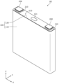
図1は、実施の形態に係る蓄電素子の外観を示す斜視図である。FIG. 1 is a perspective view showing the appearance of a power storage element according to an embodiment. 図2は、実施の形態に係る蓄電素子の容器内方に配置されている構成要素を示す斜視図である。FIG. 2 is a perspective view showing the components arranged inside the container of the power storage element according to the embodiment. 図3は、実施の形態に係る蓄電素子を分解して各構成要素を示す分解斜視図である。FIG. 3 is an exploded perspective view showing each component of the power storage element according to the embodiment. 図4は、実施の形態に係る電極体、集電体、当て板及びレーザ溶接部の構成を示す正面図及び断面図である。FIG. 4 is a front view and a sectional view showing the configuration of an electrode body, a current collector, a backing plate, and a laser welding part according to the embodiment. 図5は、実施の形態に係る電極体と集電体とをレーザ溶接してレーザ溶接部を形成する方法を示す断面図である。FIG. 5 is a cross-sectional view showing a method of forming a laser welded portion by laser welding the electrode body and current collector according to the embodiment. 図6は、実施の形態の変形例1に係るレーザ溶接部の構成を示す断面図である。FIG. 6 is a sectional view showing the configuration of a laser welding part according to Modification 1 of the embodiment. 図7は、実施の形態の変形例2に係るレーザ溶接部の構成を示す断面図である。FIG. 7 is a sectional view showing the configuration of a laser welding part according to a second modification of the embodiment. 図8は、実施の形態の変形例3に係るレーザ溶接部の構成を示す断面図である。FIG. 8 is a cross-sectional view showing the configuration of a laser welding part according to modification 3 of the embodiment. 図9Aは、実施の形態の変形例4に係るレーザ溶接部の構成を示す断面図である。FIG. 9A is a cross-sectional view showing the configuration of a laser welding part according to Modification 4 of the embodiment. 図9Bは、実施の形態の変形例5に係るレーザ溶接部の構成を示す断面図である。FIG. 9B is a cross-sectional view showing the configuration of a laser welding part according to modification 5 of the embodiment.

本発明の一態様に係る蓄電素子は、極板が積層された積層部を有する電極体と、前記積層部に接続される集電体と、を備える蓄電素子であって、前記積層部は、第一方向において、前記集電体の一部である第一部と、前記集電体の他の一部または当て板である第二部とで挟まれた状態で配置され、前記第一部及び前記第二部の少なくとも一方は、他方に向けて突出する凸部が形成された突出部を有し、前記他方の少なくとも一部は、前記第一方向において、前記突出部とで前記積層部を挟む位置に配置され、前記第一部及び前記第二部の間における前記突出部と隣り合う位置には、隙間が形成され、前記第一方向から見て前記突出部と重なる位置に、前記第一部と前記積層部とがレーザ溶接されたレーザ溶接部が形成されている。 A power storage element according to one aspect of the present invention includes an electrode body having a laminated portion in which electrode plates are laminated, and a current collector connected to the laminated portion, the laminated portion comprising: In a first direction, the first part is sandwiched between a first part that is a part of the current collector and a second part that is another part of the current collector or a backing plate; and at least one of the second parts has a protrusion formed with a convex part that protrudes toward the other, and at least a part of the other part is connected to the laminated part with the protrusion in the first direction. A gap is formed at a position adjacent to the protrusion between the first part and the second part, and a gap is formed at a position overlapping with the protrusion when viewed from the first direction. A laser welded portion is formed by laser welding the first portion and the laminated portion.

これによれば、蓄電素子は、第一方向において、集電体の一部である第一部と、集電体の他の一部または当て板である第二部とで挟まれた状態で配置される積層部を有することを含む。第一部及び第二部の少なくとも一方は、他方に向けて突出する凸部が形成された突出部を有し、他方の少なくとも一部は、第一方向において、突出部とで積層部を挟む位置に配置されることを含む。第一部及び第二部の間における突出部と隣り合う位置には、隙間が形成され、第一方向から見て突出部と重なる位置に、第一部と積層部とがレーザ溶接されたレーザ溶接部が形成されていることを含む。つまり、第一部及び第二部の少なくとも一方(集電体又は当て板)に、他方に向けて突出する凸部が形成された突出部を設けて積層部に当て、他方の少なくとも一部とで積層部を挟むことで、部材同士の境界面が圧迫される。この際、第一部及び第二部の間における突出部と隣り合う位置には、隙間が形成されることとなる。これにより、積層部における極板の浮きが抑制される。つまり、レーザ溶接対象部位に隙間が生じることが抑制されることで、電極体の積層部と集電体との接合の品質の向上を図ることができる。 According to this, the electricity storage element is sandwiched in the first direction between the first part, which is a part of the current collector, and the second part, which is another part of the current collector or the backing plate. The method includes having a laminated portion disposed. At least one of the first part and the second part has a protrusion formed with a convex part that protrudes toward the other, and at least a part of the other part sandwiches the laminated part between the protrusion and the protrusion in the first direction. including being placed in a position. A gap is formed between the first part and the second part at a position adjacent to the protrusion, and the first part and the laminated part are laser welded at a position overlapping the protrusion when viewed from the first direction. This includes the formation of welds. That is, at least one of the first part and the second part (the current collector or the backing plate) is provided with a protrusion in which a convex part is formed that protrudes toward the other, and the protrusion is applied to the laminated part, and at least a part of the other By sandwiching the laminated portion between the members, the interface between the members is compressed. At this time, a gap will be formed between the first part and the second part at a position adjacent to the protruding part. This suppresses floating of the electrode plates in the laminated portion. That is, by suppressing the formation of a gap in the laser welding target site, it is possible to improve the quality of the bond between the laminated portion of the electrode body and the current collector.

前記突出部は、前記凸部と対向する位置に、前記凸部に向けて凹んだ凹部を有してもよい。 The protrusion may have a recess that is recessed toward the protrusion at a position facing the protrusion.

これによれば、突出部が、凸部と対向する位置に凸部に向けて凹んだ凹部を有することで、突出部の厚みが薄くなるため、レーザ溶接時の出力を下げられる。このため、レーザ溶接部の温度上昇を抑制できる。したがって、さらに電極体の積層部と集電体との接合の品質の向上を図ることができる。 According to this, since the protruding part has a recessed part recessed toward the protruding part at a position facing the protruding part, the thickness of the protruding part becomes thinner, so that the output during laser welding can be lowered. Therefore, it is possible to suppress the temperature rise in the laser welded portion. Therefore, it is possible to further improve the quality of the bond between the laminated portion of the electrode body and the current collector.

前記突出部の突出部分の厚みは、前記第一部及び前記第二部の少なくとも一方の、前記突出部と隣り合う部位の厚みよりも薄くてもよい。 The thickness of the protruding portion of the protruding portion may be thinner than the thickness of a portion of at least one of the first portion and the second portion adjacent to the protruding portion.

これによれば、突出部の突出部分の厚みは、第一部及び第二部の少なくとも一方の、突出部と隣り合う部位の厚みよりも薄くされることで、さらにレーザ溶接時の出力を下げられる。このため、レーザ溶接部の温度上昇をさらに抑制できる。したがって、さらに電極体の積層部と集電体との接合の品質の向上を図ることができる。 According to this, the thickness of the protruding part of the protruding part is made thinner than the thickness of the part adjacent to the protruding part of at least one of the first part and the second part, thereby further reducing the output power during laser welding. It will be done. Therefore, the temperature rise in the laser welded portion can be further suppressed. Therefore, it is possible to further improve the quality of the bond between the laminated portion of the electrode body and the current collector.

前記第一部及び前記第二部の一方は、前記凸部としての第一凸部を有し、前記第一部及び前記第二部の他方は、前記第一凸部と対向する位置に、前記第一凸部よりも大きな平面、又は、前記第一凸部に向けて突出する前記凸部としての第二凸部を有してもよい。 One of the first part and the second part has a first convex part as the convex part, and the other of the first part and the second part is at a position facing the first convex part, It may have a larger plane than the first protrusion, or a second protrusion as the protrusion that protrudes toward the first protrusion.

これによれば、第一部及び第二部の一方は、凸部としての第一凸部を有し、第一部及び第二部の他方は、第一凸部と対向する位置に、第一凸部よりも大きな平面、又は、第一凸部に向けて突出する凸部としての第二凸部を有することで、突出部を容易に積層部に当て、部材同士の境界面を容易に接触させられる。このため、さらに積層部における極板の浮きが抑制され、レーザ溶接対象部位の隙間が抑制できる。したがって、さらに電極体の積層部と集電体との接合の品質の向上を図ることができる。 According to this, one of the first part and the second part has the first convex part as the convex part, and the other of the first part and the second part has the first convex part at a position opposite to the first convex part. By having a flat surface larger than the first protrusion or a second protrusion that protrudes toward the first protrusion, the protrusion can be easily applied to the laminated part and the interface between the members can be easily be brought into contact. For this reason, floating of the electrode plate in the laminated portion is further suppressed, and the gap at the laser welding target area can be suppressed. Therefore, it is possible to further improve the quality of the bond between the laminated portion of the electrode body and the current collector.

前記第一方向と直交する第二方向において、前記第一部及び前記第二部の間における前記突出部を挟む位置に、一対の前記隙間が形成されてもよい。 In a second direction perpendicular to the first direction, a pair of the gaps may be formed at positions sandwiching the protrusion between the first part and the second part.

これによれば、第一方向と直交する第二方向において、第一部及び第二部の間における突出部を挟む位置に、一対の隙間が形成されることで、より容易に突出部を積層部に当てられる。このため、突出部をよりバランスよく圧迫できる。したがって、さらに電極体の積層部と集電体との接合の品質の向上を図ることができる。 According to this, a pair of gaps are formed at positions sandwiching the protrusion between the first part and the second part in the second direction orthogonal to the first direction, so that the protrusion can be laminated more easily. assigned to the department. Therefore, the protrusion can be compressed in a more balanced manner. Therefore, it is possible to further improve the quality of the bond between the laminated portion of the electrode body and the current collector.

前記レーザ溶接部は、前記第一方向において、前記第一部及び前記第二部の少なくとも一方を貫通して形成されてもよい。 The laser welded portion may be formed to penetrate at least one of the first part and the second part in the first direction.

これによれば、レーザ溶接部は、第一方向において、第一部及び第二部の当該一方を貫通して形成されることで、他方に向けて突出する凸部が形成された突出部を貫通して形成されることになる。つまり、さらに積層部における極板の浮きが抑制され、レーザ溶接対象部位の隙間が抑制できる。したがって、さらに電極体の積層部と集電体との接合の品質の向上を図ることができる。 According to this, the laser welded part is formed by penetrating one of the first part and the second part in the first direction, so that the protrusion part in which the convex part protrudes toward the other part is formed. It will be formed through it. In other words, the floating of the electrode plates in the laminated portion is further suppressed, and the gap at the laser welding target area can be suppressed. Therefore, it is possible to further improve the quality of the bond between the laminated portion of the electrode body and the current collector.

本発明の別の一態様に係る蓄電素子は、極板が積層された積層部を有する電極体と、前記積層部に接続される集電体とを備える蓄電素子であって、前記積層部は、第一方向において、前記集電体の一部である第一部と並んだ状態で配置され、前記第一部は、前記積層部に向けて突出する凸部が形成された突出部を有し、前記第一部及び前記積層部の間における前記突出部と隣り合う位置には、隙間が形成され、前記第一方向から見て前記突出部と重なる位置に、前記第一部と前記積層部とがレーザ溶接されたレーザ溶接部が形成され、前記レーザ溶接部は、前記第一方向において、前記第一部と前記積層部とを貫通して形成されている。 A power storage element according to another aspect of the present invention includes an electrode body having a laminated portion in which electrode plates are laminated, and a current collector connected to the laminated portion, wherein the laminated portion is , disposed in a first direction in line with a first part that is a part of the current collector, and the first part has a protrusion in which a protrusion protrudes toward the laminated part. A gap is formed between the first part and the laminated part at a position adjacent to the protruding part, and a gap is formed between the first part and the laminated part at a position overlapping with the protruding part when viewed from the first direction. A laser welded portion is formed by laser welding the first portion and the laminated portion, and the laser welded portion is formed to penetrate the first portion and the laminated portion in the first direction.

これによれば、蓄電素子において、第一方向において、集電体の一部である第一部と並んだ状態で配置される積層部を有し、第一部は、積層部に向けて突出する凸部が形成された突出部を有することを含む。第一部及び積層部の間における突出部と隣り合う位置には、隙間が形成され、第一方向から見て突出部と重なる位置に、第一部と積層部とがレーザ溶接されたレーザ溶接部が形成され、レーザ溶接部は、第一方向において、第一部と積層部を貫通して形成されることを含む。つまり、積層部に向けて突出する凸部が形成された突出部が設けられた第一部を積層部に当て、接合時に第一部と治具とで積層部を挟むことで、部材同士の境界面が圧迫される。この際、第一部及び積層部の間における突出部と隣り合う位置には、隙間が形成されることとなる。これにより、積層部における極板の浮きが抑制され、レーザ溶接対象部位の隙間が抑制できる。したがって、電極体の積層部と集電体との接合の品質の向上を図ることができる。 According to this, the power storage element has a laminated part arranged in a first direction in line with a first part that is a part of the current collector, and the first part protrudes toward the laminated part. This includes having a protrusion formed with a convex portion. A gap is formed between the first part and the laminated part at a position adjacent to the protruding part, and the first part and the laminated part are laser welded at a position overlapping with the protruding part when viewed from the first direction. A portion is formed, and a laser weld is formed in a first direction through the first portion and the laminated portion. In other words, the first part, which is provided with a protruding part that projects toward the laminated part, is applied to the laminated part, and the laminated part is sandwiched between the first part and the jig during joining, so that the parts can be bonded together. Boundary surfaces are pressured. At this time, a gap will be formed between the first part and the laminated part at a position adjacent to the protrusion. As a result, lifting of the electrode plates in the laminated portion can be suppressed, and a gap in the laser welding target area can be suppressed. Therefore, it is possible to improve the quality of bonding between the laminated portion of the electrode body and the current collector.

以下、図面を参照しながら、本発明の実施の形態(及びその変形例)に係る蓄電素子について説明する。以下で説明する実施の形態は、いずれも包括的または具体的な例を示すものである。以下の実施の形態で示される数値、形状、材料、構成要素、構成要素の配置位置及び接続形態、製造工程、製造工程の順序などは、一例であり、本発明を限定する主旨ではない。各図において、寸法等は厳密に図示したものではない。各図において、同一または同様な構成要素については同じ符号を付している。 Hereinafter, a power storage element according to an embodiment (and a modification thereof) of the present invention will be described with reference to the drawings. The embodiments described below are all inclusive or specific examples. The numerical values, shapes, materials, components, arrangement positions and connection forms of the components, manufacturing steps, order of manufacturing steps, etc. shown in the following embodiments are merely examples, and do not limit the present invention. In each figure, dimensions etc. are not strictly illustrated. In each figure, the same or similar components are designated by the same reference numerals.

以下の説明及び図面中において、蓄電素子が有する一対(正極及び負極、以下同様)の電極端子の並び方向、一対の集電体の並び方向、または、容器の短側面の対向方向を、X軸方向と定義する。容器の長側面の対向方向、容器の厚さ方向、電極体と集電体との接合部(レーザ溶接部)における極板の積層方向、当該接合部における集電体と電極体との並び方向、当該接合部における集電体と電極体と当て板との並び方向、または、当該接合部におけるレーザ光の照射方向を、Y軸方向と定義する。蓄電素子の容器本体と蓋体との並び方向、集電体の電極接続部(脚部)の延びる方向、または、上下方向を、Z軸方向と定義する。これらX軸方向、Y軸方向及びZ軸方向は、互いに交差(本実施の形態では直交)する方向である。使用態様によってはZ軸方向が上下方向にならない場合も考えられるが、以下では説明の便宜のため、Z軸方向を上下方向として説明する。 In the following description and drawings, the direction in which a pair of electrode terminals (positive electrode and negative electrode, the same shall apply hereinafter) of a power storage element, the direction in which a pair of current collectors are arranged, or the direction in which the short sides of the container face each other is referred to as the X axis. Define direction. The direction in which the long sides of the container face each other, the thickness direction of the container, the stacking direction of the electrode plates at the joint between the electrode body and the current collector (laser welding part), and the alignment direction of the current collector and the electrode body at the joint. , the direction in which the current collector, electrode body, and backing plate are lined up at the joint, or the direction in which the laser beam is irradiated at the joint is defined as the Y-axis direction. The direction in which the container body and the lid of the power storage element are lined up, the direction in which the electrode connection portions (legs) of the current collector extend, or the up-down direction is defined as the Z-axis direction. These X-axis direction, Y-axis direction, and Z-axis direction are directions that intersect with each other (orthogonal in this embodiment). Depending on the usage mode, the Z-axis direction may not be the vertical direction, but for convenience of explanation, the Z-axis direction will be described as the vertical direction below.

以下の説明において、X軸プラス方向とは、X軸の矢印方向を示し、X軸マイナス方向とは、X軸プラス方向とは反対方向を示す。Y軸方向及びZ軸方向についても同様である。以下では、Y軸方向を第一方向とも呼び、X軸方向を第二方向とも呼ぶ。平行及び直交などの、相対的な方向または姿勢を示す表現は、厳密には、その方向または姿勢ではない場合も含む。2つの方向が直交している、とは、当該2つの方向が完全に直交していることを意味するだけでなく、実質的に直交していること、すなわち、数%程度の差異を含んでもよい。以下の説明において、「絶縁」と表現する場合、「電気的な絶縁」を意味する。 In the following description, the X-axis plus direction refers to the arrow direction of the X-axis, and the X-axis minus direction refers to the opposite direction to the X-axis plus direction. The same applies to the Y-axis direction and the Z-axis direction. Hereinafter, the Y-axis direction will also be referred to as the first direction, and the X-axis direction will also be referred to as the second direction. Expressions indicating relative directions or orientations, such as parallel and orthogonal, include cases where the directions or orientations are not strictly speaking. Two directions being orthogonal does not only mean that the two directions are completely orthogonal, but also that they are substantially orthogonal, even if there is a difference of a few percent. good. In the following description, when the expression "insulation" is used, it means "electrical insulation".

(実施の形態)
[1 蓄電素子10の全般的な説明]
まず、図1~図3を用いて、本実施の形態における蓄電素子10の全般的な説明を行う。図1は、本実施の形態に係る蓄電素子10の外観を示す斜視図である。図2は、本実施の形態に係る蓄電素子10の容器100の内方に配置されている構成要素を示す斜視図である。具体的には、図2は、蓄電素子10から容器本体110を分離した状態での構成を示す斜視図であり、電極体300に集電体400を接合した後の状態を示している。図3は、本実施の形態に係る蓄電素子10を分解して各構成要素を示す分解斜視図である。具体的には、図3は、図2に示した容器本体110以外の構成要素を分解して示す斜視図であり、電極体300に集電体400を接合する前の状態を示している。
(Embodiment)
[1 General description of power storage element 10]
First, a general description of the power storage element 10 in this embodiment will be given using FIGS. 1 to 3. FIG. 1 is a perspective view showing the appearance of a power storage element 10 according to the present embodiment. FIG. 2 is a perspective view showing components arranged inside container 100 of power storage element 10 according to the present embodiment. Specifically, FIG. 2 is a perspective view showing the configuration with the container body 110 separated from the power storage element 10, and shows the state after the current collector 400 is joined to the electrode body 300. FIG. 3 is an exploded perspective view showing each component of the power storage element 10 according to the present embodiment. Specifically, FIG. 3 is an exploded perspective view showing components other than the container body 110 shown in FIG. 2, and shows a state before the current collector 400 is joined to the electrode body 300.

蓄電素子10は、電気を充電し、電気を放電することのできる二次電池(単電池)であり、具体的には、リチウムイオン二次電池等の非水電解質二次電池である。蓄電素子10は、自動車、自動二輪車、ウォータークラフト、船舶、スノーモービル、農業機械、建設機械、または、電気鉄道用の鉄道車両等の移動体の駆動用またはエンジン始動用等のバッテリ等として用いられてもよい。上記の自動車としては、電気自動車(EV)、ハイブリッド電気自動車(HEV)、プラグインハイブリッド電気自動車(PHEV)及び化石燃料(ガソリン、軽油、液化天然ガス等)自動車が例示される。上記の電気鉄道用の鉄道車両としては、電車、モノレール、リニアモーターカー、並びに、ディーゼル機関及び電気モーターの両方を備えるハイブリッド電車が例示される。蓄電素子10は、家庭用または事業用等に使用される定置用のバッテリ等としても用いられてもよい。 The power storage element 10 is a secondary battery (single battery) that can charge and discharge electricity, and specifically, is a non-aqueous electrolyte secondary battery such as a lithium ion secondary battery. The power storage element 10 is used as a battery for driving or starting an engine of a moving object such as an automobile, a motorcycle, a watercraft, a ship, a snowmobile, an agricultural machine, a construction machine, or a railway vehicle for an electric railway. It's okay. Examples of the above-mentioned vehicles include electric vehicles (EVs), hybrid electric vehicles (HEVs), plug-in hybrid electric vehicles (PHEVs), and fossil fuel (gasoline, diesel oil, liquefied natural gas, etc.) vehicles. Examples of the above-mentioned railway vehicles for electric railways include electric trains, monorails, linear motor cars, and hybrid electric trains equipped with both a diesel engine and an electric motor. The power storage element 10 may also be used as a stationary battery or the like used for home or business purposes.

蓄電素子10は、非水電解質二次電池には限定されず、非水電解質二次電池以外の二次電池であってもよいし、キャパシタであってもよい。蓄電素子10は、二次電池ではなく、使用者が充電をしなくても蓄えられている電気を使用できる一次電池であってもよい。蓄電素子10は、固体電解質を用いた電池であってもよい。蓄電素子10は、パウチタイプの蓄電素子であってもよい。本実施の形態では、扁平な直方体形状(角形)の蓄電素子10を図示しているが、蓄電素子10の形状は、直方体形状には限定されず、円柱形状、長円柱形状または直方体以外の多角柱形状等であってもよい。 The power storage element 10 is not limited to a non-aqueous electrolyte secondary battery, and may be a secondary battery other than a non-aqueous electrolyte secondary battery, or a capacitor. The power storage element 10 may be not a secondary battery but a primary battery that allows the user to use the stored electricity without charging it. Power storage element 10 may be a battery using a solid electrolyte. The power storage element 10 may be a pouch type power storage element. In this embodiment, a flat rectangular parallelepiped-shaped (prismatic) power storage element 10 is illustrated, but the shape of the power storage element 10 is not limited to the rectangular parallelepiped shape, and may be a cylinder shape, an elongated cylinder shape, or a shape other than a rectangular parallelepiped. It may also have a prismatic shape or the like.

図1に示すように、蓄電素子10は、容器100と、一対(正極及び負極)の電極端子200と、一対(正極及び負極)の上部ガスケット210と、を備えている。図2及び図3に示すように、容器100の内方には、一対(正極及び負極)の下部ガスケット220と、電極体300と、一対(正極及び負極)の集電体400(404及び405)と、一対(正極及び負極)の当て板500と、が収容されている。容器100の内部には、電解液(非水電解質)が封入されているが、図示は省略する。当該電解液としては、蓄電素子10の性能を損なうものでなければその種類に特に制限はなく、様々なものを選択することができる。上記の構成要素の他、電極体300の側方または下方等に配置されるスペーサ、電極体300等を包み込む絶縁フィルム等が配置されてもよい。 As shown in FIG. 1, the power storage element 10 includes a container 100, a pair of electrode terminals 200 (a positive electrode and a negative electrode), and a pair of upper gaskets 210 (a positive electrode and a negative electrode). As shown in FIGS. 2 and 3, inside the container 100, there are a pair (positive electrode and negative electrode) of lower gaskets 220, an electrode body 300, and a pair (positive electrode and negative electrode) of current collectors 400 (404 and 405). ) and a pair (positive electrode and negative electrode) of backing plates 500 are housed. An electrolytic solution (non-aqueous electrolyte) is sealed inside the container 100, but illustration thereof is omitted. The type of electrolytic solution is not particularly limited as long as it does not impair the performance of the power storage element 10, and various types can be selected. In addition to the above-mentioned components, a spacer disposed on the side or below the electrode body 300, an insulating film that wraps around the electrode body 300, etc. may be disposed.

容器100は、開口が形成された容器本体110と、容器本体110の当該開口を閉塞する蓋体120と、を有する直方体形状(角形または箱形)のケースである。容器本体110は、容器100の本体部を構成する矩形筒状で底を備える部材である。容器本体110は、X軸方向両側の側面(短側面)に一対の平板状かつ矩形状の短側壁部111を有し、Y軸方向両側の側面(長側面)に一対の平板状かつ矩形状の長側壁部112を有し、Z軸マイナス方向に平板状かつ矩形状の底壁部113を有している。蓋体120は、容器100の蓋部を構成する矩形状の板状部材であり、容器本体110のZ軸プラス方向にX軸方向に延びて配置されている。蓋体120には、容器100の内方の圧力が過度に上昇した場合に当該圧力を開放するガス排出弁121、及び、容器100の内方に電解液を注液するための注液部122等が設けられている。 The container 100 is a rectangular parallelepiped-shaped (prismatic or box-shaped) case that includes a container body 110 with an opening formed therein and a lid 120 that closes the opening of the container body 110. The container body 110 is a rectangular cylindrical member that constitutes the main body of the container 100 and has a bottom. The container body 110 has a pair of flat and rectangular short side walls 111 on both sides (short sides) in the X-axis direction, and a pair of flat and rectangular short side walls 111 on both sides (long sides) in the Y-axis direction. It has a long side wall portion 112 and a bottom wall portion 113 that is flat and rectangular in the negative Z-axis direction. The lid 120 is a rectangular plate-like member that constitutes the lid of the container 100, and is arranged to extend in the X-axis direction in the Z-axis plus direction of the container body 110. The lid body 120 includes a gas discharge valve 121 that releases the pressure inside the container 100 when the pressure rises excessively, and a liquid injection part 122 that injects electrolyte into the inside of the container 100. etc. are provided.

このような構成により、容器100は、電極体300等を容器本体110の内部に収容後、容器本体110と蓋体120とが溶接等によって接合されることにより、内部が密封される構造となっている。容器100(容器本体110及び蓋体120)の材質は特に限定されず、ステンレス鋼、アルミニウム、アルミニウム合金、鉄など溶接可能な金属としてもよく、樹脂を用いてもよい。 With this configuration, the container 100 has a structure in which the inside is sealed by housing the electrode body 300 and the like inside the container body 110 and then joining the container body 110 and the lid 120 by welding or the like. ing. The material of the container 100 (container body 110 and lid 120) is not particularly limited, and may be a weldable metal such as stainless steel, aluminum, aluminum alloy, or iron, or resin may be used.

電極体300は、正極板と負極板とセパレータとを備え、電気を蓄えることができる蓄電要素(発電要素)である。正極板は、アルミニウムまたはアルミニウム合金等からなる長尺帯状の集電箔である正極基材層上に正極活物質層が形成された極板である。負極板は、銅または銅合金等からなる長尺帯状の集電箔である負極基材層上に負極活物質層が形成された極板である。上記集電箔として、ニッケル、鉄、ステンレス鋼、チタン、焼成炭素、導電性高分子、導電性ガラス、Al-Cd合金など、適宜公知の材料を用いることもできる。正極活物質層及び負極活物質層に用いられる正極活物質及び負極活物質としては、リチウムイオンを吸蔵放出可能な活物質であれば、適宜公知の材料を使用できる。セパレータは、樹脂からなる微多孔性のシートまたは不織布等を用いることができる。 The electrode body 300 is a power storage element (power generation element) that includes a positive electrode plate, a negative electrode plate, and a separator and can store electricity. The positive electrode plate is an electrode plate in which a positive electrode active material layer is formed on a positive electrode base material layer which is a long strip-shaped current collecting foil made of aluminum or an aluminum alloy. The negative electrode plate is an electrode plate in which a negative electrode active material layer is formed on a negative electrode base material layer which is a long strip-shaped current collecting foil made of copper or a copper alloy. As the current collector foil, appropriately known materials such as nickel, iron, stainless steel, titanium, fired carbon, conductive polymer, conductive glass, Al--Cd alloy, etc. can be used. As the positive electrode active material and the negative electrode active material used in the positive electrode active material layer and the negative electrode active material layer, any known material can be used as appropriate as long as it is an active material capable of intercalating and deintercalating lithium ions. As the separator, a microporous sheet made of resin, a nonwoven fabric, or the like can be used.

電極体300は、極板301が積層された積層部320を有する。つまり、電極体300は、正極板と負極板とセパレータとが積層されて形成されている。具体的には、電極体300は、正極板と負極板との間にセパレータが配置され巻回されて形成されている。さらに具体的には、電極体300は、正極板と負極板とが、セパレータを介して、巻回軸の方向に互いにずらして巻回されている。巻回軸とは、正極板及び負極板等を巻回する際の中心軸となる仮想的な軸であり、本実施の形態では、電極体300の中心を通る、X軸方向に平行な直線である。正極板及び負極板は、それぞれのずらされた方向の端部に、活物質が形成(塗工)されず基材層が露出した部分(活物質層非形成部)を有している。 The electrode body 300 has a laminated portion 320 in which electrode plates 301 are laminated. That is, the electrode body 300 is formed by laminating a positive electrode plate, a negative electrode plate, and a separator. Specifically, the electrode body 300 is formed by winding a separator between a positive electrode plate and a negative electrode plate. More specifically, in the electrode body 300, a positive electrode plate and a negative electrode plate are wound with a separator interposed therebetween so as to be offset from each other in the direction of the winding axis. The winding axis is a virtual axis that becomes the central axis when winding the positive electrode plate, negative electrode plate, etc., and in this embodiment, it is a straight line parallel to the X-axis direction passing through the center of the electrode body 300. It is. The positive electrode plate and the negative electrode plate each have a portion (active material layer non-forming portion) where the active material is not formed (coated) and the base material layer is exposed at the ends in the shifted direction.

これにより、電極体300は、巻回軸方向の一端部に、正極板の活物質層非形成部が積層されて束ねられた正極の積層部320を有し、巻回軸方向の他端部に、負極板の活物質層非形成部が積層されて束ねられた負極の積層部320を有している。積層部320は、極板(正極板または負極板)が積層方向(Y軸方向)に積層された部位である。つまり、電極体300は、電極体300の本体を構成する電極体本体部310と、電極体本体部310からX軸方向両側に突出した一対(正極及び負極)の積層部320と、を有している。電極体本体部310は、正極板及び負極板の活物質層が形成(塗工)された部分とセパレータとが巻回されて形成された長円形状の部位(活物質層形成部)である。本実施の形態では、電極体300(電極体本体部310)の断面形状として長円形状を図示しているが、円形状、楕円形状、または、多角形状等でもよい。 As a result, the electrode body 300 has a positive electrode laminated portion 320 in which active material layer-free portions of the positive electrode plate are laminated and bundled at one end in the winding axis direction, and the other end in the winding axis direction. It has a negative electrode laminated portion 320 in which the active material layer-free portion of the negative electrode plate is laminated and bundled. The laminated portion 320 is a portion where electrode plates (positive electrode plates or negative electrode plates) are laminated in the lamination direction (Y-axis direction). In other words, the electrode body 300 includes an electrode body body part 310 that constitutes the body of the electrode body 300, and a pair of laminated parts 320 (a positive electrode and a negative electrode) that protrude from the electrode body body part 310 on both sides in the X-axis direction. ing. The electrode main body part 310 is an oval-shaped part (active material layer forming part) formed by winding the parts of the positive electrode plate and the negative electrode plate on which the active material layers are formed (coated) and the separator. . In this embodiment, an oval shape is illustrated as the cross-sectional shape of the electrode body 300 (electrode body main body portion 310), but the cross-sectional shape may be circular, elliptical, polygonal, or the like.

電極端子200は、集電体400を介して、電極体300に電気的に接続される端子部材(正極端子及び負極端子)である。つまり、電極端子200は、電極体300に蓄えられている電気を蓄電素子10の外部空間に導出し、電極体300に電気を蓄えるために蓄電素子10の内部空間に電気を導入するための金属製の部材である。電極端子200は、アルミニウム、アルミニウム合金、銅または銅合金等の金属等の導電部材で形成されている。電極端子200は、かしめ等によって、集電体400に接続(接合)され、かつ、蓋体120に取り付けられている。 The electrode terminal 200 is a terminal member (a positive electrode terminal and a negative electrode terminal) that is electrically connected to the electrode body 300 via the current collector 400. In other words, the electrode terminal 200 is a metal terminal for guiding the electricity stored in the electrode body 300 to the external space of the electricity storage element 10 and for introducing electricity into the internal space of the electricity storage element 10 to store electricity in the electrode body 300. It is a manufactured member. The electrode terminal 200 is made of a conductive member such as metal such as aluminum, aluminum alloy, copper, or copper alloy. The electrode terminal 200 is connected (joined) to the current collector 400 by caulking or the like, and is attached to the lid 120.

具体的には、図3に示すように、電極端子200は、軸部201が、上部ガスケット210の貫通孔211と、蓋体120の貫通孔123と、下部ガスケット220の貫通孔221と、集電体400の貫通孔413とに挿入されて、かしめられることにより、集電体400とともに蓋体120に固定される。電極端子200と集電体400とを接続(接合)する手法は、かしめ接合には限定されず、超音波接合、レーザ溶接若しくは抵抗溶接等の溶接、または、ねじ締結等のかしめ以外の機械的接合等が用いられてもよい。 Specifically, as shown in FIG. 3, the shaft portion 201 of the electrode terminal 200 is connected to the through hole 211 of the upper gasket 210, the through hole 123 of the lid body 120, and the through hole 221 of the lower gasket 220. The current collector 400 is fixed to the lid 120 together with the current collector 400 by being inserted into the through hole 413 of the current collector 400 and caulked. The method of connecting (joining) the electrode terminal 200 and the current collector 400 is not limited to caulking, but may include welding such as ultrasonic welding, laser welding, or resistance welding, or a mechanical method other than caulking such as screw fastening. Bonding or the like may also be used.

上部ガスケット210は、容器100の蓋体120と電極端子200との間に配置され、蓋体120と電極端子200との間を絶縁し、かつ封止する板状かつ矩形状の部材(正極上部ガスケット及び負極上部ガスケット)である。上部ガスケット210の中央部には、上述の電極端子200の軸部201が挿入される貫通孔211が形成されている。下部ガスケット220は、容器100の蓋体120と集電体400との間に配置され、蓋体120と集電体400との間を絶縁する板状かつ矩形状の部材(正極下部ガスケット及び負極下部ガスケット)である。下部ガスケット220の中央部には、上述の電極端子200の軸部201が挿入される貫通孔221が形成されている。 The upper gasket 210 is a plate-shaped and rectangular member (a positive electrode upper gasket and negative electrode upper gasket). A through hole 211 into which the shaft portion 201 of the electrode terminal 200 described above is inserted is formed in the center of the upper gasket 210. The lower gasket 220 is a plate-shaped and rectangular member (a positive electrode lower gasket and a negative electrode lower gasket). A through hole 221 into which the shaft portion 201 of the electrode terminal 200 described above is inserted is formed in the center of the lower gasket 220.

上部ガスケット210及び下部ガスケット220は、絶縁性を有していればどのような素材で形成されてもよいが、ポリプロピレン(PP)、ポリエチレン(PE)、ポリスチレン(PS)、ポリフェニレンサルファイド樹脂(PPS)、ポリフェニレンエーテル(PPE(変性PPEを含む))、ポリエチレンテレフタラート(PET)、ポリブチレンテレフタレート(PBT)、ポリエーテルエーテルケトン(PEEK)、テトラフルオロエチレン・パーフルオロアルキルビニルエーテル(PFA)、ポリテトラフルオロエチレン(PTFE)、ポリエーテルサルフォン(PES)、ABS樹脂、若しくは、それらの複合材料等の絶縁部材により形成されてもよい。 The upper gasket 210 and the lower gasket 220 may be made of any material as long as it has insulating properties, such as polypropylene (PP), polyethylene (PE), polystyrene (PS), polyphenylene sulfide resin (PPS). , polyphenylene ether (PPE (including modified PPE)), polyethylene terephthalate (PET), polybutylene terephthalate (PBT), polyether ether ketone (PEEK), tetrafluoroethylene perfluoroalkyl vinyl ether (PFA), polytetrafluoro It may be formed of an insulating member such as ethylene (PTFE), polyethersulfone (PES), ABS resin, or a composite material thereof.

集電体400は、電極体300の積層部320に接続されている。具体的には、集電体400は、電極体300のX軸方向両側に配置され、電極体300の積層部320と電極端子200とに接続(接合)されて、電極体300と電極端子200とを電気的に接続する導電性と剛性とを備えた集電部材(正極集電体及び負極集電体)である。さらに具体的には、集電体400は、容器本体110の側壁から蓋体120に亘って当該側壁及び蓋体120に沿って屈曲して配置される板状部材である。集電体400は、蓋体120に固定して接続(接合)される。この構成により、電極体300が、集電体400によって蓋体120から吊り下げられた状態で保持(支持)され、振動や衝撃等による揺れが抑制される。集電体400の材質は特に限定されないが、正極の集電体400は、電極体300の正極基材層と同様、アルミニウムまたはアルミニウム合金等で形成され、負極の集電体400は、電極体300の負極基材層と同様、銅または銅合金等で形成されてもよい。 The current collector 400 is connected to the laminated portion 320 of the electrode body 300. Specifically, the current collectors 400 are arranged on both sides of the electrode body 300 in the X-axis direction, are connected (joined) to the laminated portion 320 of the electrode body 300 and the electrode terminals 200, and are connected to the electrode body 300 and the electrode terminals 200. A current collecting member (a positive electrode current collector and a negative electrode current collector) having conductivity and rigidity that electrically connects the two. More specifically, the current collector 400 is a plate-like member that extends from the side wall of the container body 110 to the lid 120 and is bent along the side wall and the lid 120. The current collector 400 is fixedly connected (joined) to the lid 120. With this configuration, the electrode body 300 is held (supported) in a suspended state from the lid body 120 by the current collector 400, and shaking due to vibration, impact, etc. is suppressed. Although the material of the current collector 400 is not particularly limited, the positive electrode current collector 400 is made of aluminum or an aluminum alloy, like the positive electrode base material layer of the electrode body 300, and the negative electrode current collector 400 is made of aluminum or an aluminum alloy. Like the negative electrode base material layer of No. 300, it may be formed of copper, copper alloy, or the like.

図3に示すように、正極及び負極の集電体400のうちのX軸プラス方向の集電体404とX軸マイナス方向の集電体405とは、YZ平面に対して対称な形状を有している。それぞれの集電体400(404及び405)は、端子接続部414と、端子接続部414からZ軸マイナス方向に向けて延びた脚部である電極接続部420と、を有している。 As shown in FIG. 3, of the positive electrode and negative electrode current collectors 400, the current collector 404 in the positive direction of the X-axis and the current collector 405 in the negative direction of the X-axis have shapes that are symmetrical with respect to the YZ plane. are doing. Each current collector 400 (404 and 405) has a terminal connection portion 414 and an electrode connection portion 420 that is a leg extending from the terminal connection portion 414 in the negative Z-axis direction.

端子接続部414は、電極端子200に接続(接合)される集電体400の基部である。具体的には、端子接続部414は、集電体400の電極端子200側(上側、Z軸プラス方向)に配置され、かつ、上述の円形状の貫通孔413が形成されたXY平面に平行な平板状の部位であり、電極端子200に電気的及び機械的に接続(接合)される。電極接続部420は、電極体300に接続(接合)される集電体400の脚部である。つまり、電極接続部420は、集電体400の電極体300側(下側、Z軸マイナス方向)に配置される部位であり、電極体300に電気的及び機械的に接続(接合)される。具体的には、電極接続部420は、端子接続部414のY軸プラス方向の端部からZ軸マイナス方向に延びる長尺状かつ平板状の部位であり、電極体300の積層部320のY軸プラス方向に配置されて、積層部320に接合される。平板状とは完全に平らな板の形に限定されず、突起や孔を有してもよいし、一部が欠けてもよい。 The terminal connection portion 414 is the base of the current collector 400 that is connected (joined) to the electrode terminal 200. Specifically, the terminal connection part 414 is arranged on the electrode terminal 200 side (upper side, Z-axis positive direction) of the current collector 400, and parallel to the XY plane in which the above-mentioned circular through hole 413 is formed. The electrode terminal 200 is electrically and mechanically connected (joined) to the electrode terminal 200. The electrode connection portion 420 is a leg portion of the current collector 400 that is connected (joined) to the electrode body 300. That is, the electrode connection part 420 is a part disposed on the electrode body 300 side (lower side, Z-axis negative direction) of the current collector 400, and is electrically and mechanically connected (joined) to the electrode body 300. . Specifically, the electrode connecting portion 420 is a long and flat portion extending in the negative Z-axis direction from the end of the terminal connecting portion 414 in the Y-axis positive direction, and It is disposed in the positive axis direction and joined to the laminated portion 320. The flat plate shape is not limited to a completely flat plate shape, and may have protrusions or holes, or may be partially chipped.

本実施の形態では、集電体400の一部である電極接続部420は第一部の一例であり、当て板500は第二部の一例である。積層部320は、第一方向(Y軸方向)において、集電体400の一部である電極接続部420(第一部)と、当て板500(第二部)とで挟まれた状態で配置されている。具体的には、当て板500は、集電体400とで電極体300を挟む位置に配置され、集電体400とで電極体300を挟んだ状態で、集電体400とともに電極体300に接合される部材である。つまり、当て板500は、電極接続部420とで、積層部320を挟む位置に配置された、積層部320を保護するカバーである。当て板500は、Z軸プラス方向とZ軸マイナス方向にそれぞれ突出部510を有する。 In this embodiment, the electrode connection portion 420, which is a part of the current collector 400, is an example of the first part, and the backing plate 500 is an example of the second part. The laminated part 320 is sandwiched between an electrode connecting part 420 (first part), which is a part of the current collector 400, and a backing plate 500 (second part) in the first direction (Y-axis direction). It is located. Specifically, the patch plate 500 is placed at a position where the electrode body 300 is sandwiched between the current collector 400 and the contact plate 500 is placed in a position where the electrode body 300 is sandwiched between the current collector 400 and the electrode body 300 together with the current collector 400. It is a member to be joined. In other words, the cover plate 500 is a cover that protects the laminated portion 320 and is placed at a position sandwiching the laminated portion 320 between the electrode connection portion 420 and the laminated portion 320 . The backing plate 500 has protrusions 510 in the Z-axis plus direction and the Z-axis minus direction, respectively.

具体的には、当て板500は、積層部320のY軸マイナス方向に配置され、積層部320に沿ってZ軸方向に延びる平板状かつ矩形状の金属製の部材である。当て板500の突出部510は、Y軸方向において積層部320に対向するように配置される。当て板500の材質は特に限定されないが、正極の当て板500は、電極体300の正極基材層と同様、アルミニウムまたはアルミニウム合金等で形成され、負極の当て板500は、電極体300の負極基材層と同様、銅または銅合金等で形成されてもよい。平板状とは完全に平らな板の形に限定されず、突起や孔を有してもよいし、一部が欠けてもよい。 Specifically, the backing plate 500 is a flat rectangular metal member that is arranged in the negative Y-axis direction of the laminated portion 320 and extends in the Z-axis direction along the laminated portion 320. The protruding portion 510 of the backing plate 500 is arranged to face the laminated portion 320 in the Y-axis direction. Although the material of the backing plate 500 is not particularly limited, the positive electrode backing plate 500 is made of aluminum or an aluminum alloy, etc., similar to the positive electrode base material layer of the electrode body 300, and the negative electrode backing plate 500 is made of aluminum or an aluminum alloy, etc. Like the base material layer, it may be formed of copper, copper alloy, or the like. The flat plate shape is not limited to a completely flat plate shape, and may have protrusions or holes, or may be partially chipped.

このような構成により、電極接続部420と当て板500とで積層部320を挟んだ状態で、電極接続部420と積層部320と当て板500とが接合されて、当て板500に形成された突出部510にレーザ溶接部700(図2参照)が形成される。本実施の形態では、1つの電極接続部420に対して、Z軸方向に並ぶ2つの突出部510に2つのレーザ溶接部700が形成される。つまり、1つの集電体400において2つのレーザ溶接部700が形成され、1つの蓄電素子10において4つのレーザ溶接部700が形成される。 With such a configuration, the electrode connecting portion 420 and the laminated portion 320 are joined to the caul plate 500 with the laminated portion 320 sandwiched between the electrode connecting portion 420 and the caul plate 500, thereby forming the caul plate 500. A laser weld 700 (see FIG. 2) is formed on the protrusion 510. In this embodiment, two laser welded parts 700 are formed on two protrusions 510 aligned in the Z-axis direction for one electrode connection part 420. That is, two laser welds 700 are formed in one current collector 400, and four laser welds 700 are formed in one power storage element 10.

[2 レーザ溶接部700の説明]
[2.1 レーザ溶接部700の構成の説明]
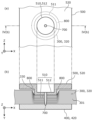
次に、電極体300の積層部320と、集電体400の電極接続部420と、当て板500の突出部510とのレーザ溶接部700の構成について、詳細に説明する。図4は、本実施の形態に係る電極体300、集電体400、当て板500及びレーザ溶接部700の構成を示す正面図及び断面図である。具体的には、図4の(a)は、図2に示したレーザ溶接部700及びその周囲の構成をY軸マイナス方向から見て拡大して示す正面図である。図4の(b)は、図4の(a)の構成を、IV(b)-IV(b)断面で切断した場合の構成を示す断面図である。図4では、図2に示したレーザ溶接部700のうちの一つのレーザ溶接部700及びその周囲の構成について示しているが、その他のレーザ溶接部700及びその周囲の構成についても、同様の構成を有している。
[2 Description of laser welding section 700]
[2.1 Description of configuration of laser welding section 700]
Next, the configuration of the laser welded portion 700 of the laminated portion 320 of the electrode body 300, the electrode connection portion 420 of the current collector 400, and the protrusion portion 510 of the backing plate 500 will be described in detail. FIG. 4 is a front view and a cross-sectional view showing the configuration of an electrode body 300, a current collector 400, a backing plate 500, and a laser welding part 700 according to the present embodiment. Specifically, (a) of FIG. 4 is an enlarged front view showing the laser welding part 700 shown in FIG. 2 and the configuration around it as viewed from the negative direction of the Y-axis. FIG. 4(b) is a sectional view showing the configuration of FIG. 4(a) taken along the IV(b)-IV(b) cross section. Although FIG. 4 shows the configuration of one of the laser welded parts 700 shown in FIG. 2 and its surroundings, the other laser welded parts 700 and their surroundings have similar structures. have.

これらの図に示すように、電極体300の積層部320のY軸プラス方向に集電体400の電極接続部420が配置され、かつ、積層部320のY軸マイナス方向に当て板500が配置されて、電極体300、集電体400及び当て板500が接合されたレーザ溶接部700が形成されている。当て板500は、上述した突出部510に加えて、突出部510と隣り合う位置に、平坦な部位(非突出部)である平坦部520を有している。突出部510は、平坦部520からY軸プラス方向に膨出した、Y軸方向から見て円形状の部位(膨出部)である。平坦部520は、Y軸方向から見て、突出部510の周囲(全周)を囲むように配置される環状の部位である。平坦部とは完全に平面となる形状に限定されない。つまり、平坦部は、平坦といえる程度に凹凸形状を有してもよいし、一部が欠けてもよいし、傾斜してもよい。 As shown in these figures, the electrode connection part 420 of the current collector 400 is arranged in the Y-axis positive direction of the laminated part 320 of the electrode body 300, and the backing plate 500 is arranged in the Y-axis negative direction of the laminated part 320. As a result, a laser welded portion 700 is formed in which the electrode body 300, the current collector 400, and the backing plate 500 are joined. In addition to the protrusion 510 described above, the backing plate 500 has a flat portion 520 that is a flat portion (non-protrusion) at a position adjacent to the protrusion 510 . The protruding portion 510 is a circular portion (bulging portion) that bulges out from the flat portion 520 in the Y-axis plus direction when viewed from the Y-axis direction. The flat portion 520 is an annular portion disposed so as to surround the periphery (entire circumference) of the protrusion portion 510 when viewed from the Y-axis direction. The flat portion is not limited to a completely flat shape. That is, the flat portion may have an uneven shape to the extent that it can be called flat, may be partially chipped, or may be sloped.

図4に示すように、突出部510は、Y軸プラス方向に向けて(積層部320に向けて)突出した凸部511と、凸部511と対向する位置に形成され、かつ、凸部511に向けて凹んだ凹部512とを有している。つまり、突出部510が、凸部511と対向する位置に、凸部511に向けて凹んだ凹部512を有している。凸部511は、平坦部520のY軸プラス方向の面からY軸プラス方向に突出した、Y軸方向から見て円形状の凸部である。凹部512は、平坦部520のY軸マイナス方向の面からY軸プラス方向に凹んだ、Y軸方向から見て円形状の凹部である。凹部512の内周面は、Y軸方向から見て、凸部511の外周面よりも小さい。つまり、当て板500のY軸マイナス方向の面が凹むことで、凹部512が形成され、かつ、当て板500のY軸プラス方向の面が突出して、凹部512と反対側の位置に、凸部511が形成される。 As shown in FIG. 4, the protrusion 510 is formed at a position opposite to the protrusion 511 that protrudes in the positive direction of the Y-axis (toward the laminated portion 320), and the protrusion 510 It has a concave portion 512 that is concave toward. That is, the protrusion 510 has a recess 512 that is recessed toward the protrusion 511 at a position facing the protrusion 511 . The convex portion 511 is a circular convex portion that protrudes in the Y-axis positive direction from the Y-axis positive direction surface of the flat portion 520 when viewed from the Y-axis direction. The recess 512 is a circular recess that is recessed in the Y-axis positive direction from the surface of the flat portion 520 in the Y-axis negative direction when viewed from the Y-axis direction. The inner circumferential surface of the recessed portion 512 is smaller than the outer circumferential surface of the convex portion 511 when viewed from the Y-axis direction. In other words, the surface of the backing plate 500 in the negative direction of the Y-axis is recessed to form a recess 512, and the surface of the backing plate 500 in the positive direction of the Y-axis protrudes to form a convex portion at a position opposite to the recess 512. 511 is formed.

図4の(b)に示すように、突出部510の突出部分の厚み(Y軸方向の厚み)は、電極接続部420(第一部)及び当て板500(第二部)の少なくとも一方(本実施の形態では当て板500)の、突出部510と隣り合う部位(本実施の形態では平坦部520)の厚み(Y軸方向の厚み)よりも薄くなっている。このように、電極接続部420(第一部)及び当て板500(第二部)の少なくとも一方(本実施の形態では当て板500)は、他方(本実施の形態では電極接続部420)に向けて突出する凸部511が形成された突出部510を有している。当該他方(電極接続部420)の少なくとも一部は、第一方向(Y軸方向)において、突出部510とで積層部320を挟む位置に配置されている。当て板500の突出部410によって積層部320が圧迫されるが、当て板500の平坦部520と積層部320とは接触しておらず、隙間があいている。レーザ溶接部700は突出部510に形成されるため、平坦部520と積層部320との間の隙間はあいていてもよいし、あいていなくてもよい。 As shown in FIG. 4(b), the thickness of the protruding portion of the protruding portion 510 (thickness in the Y-axis direction) is equal to at least one of the electrode connecting portion 420 (first part) and the backing plate 500 (second part) In this embodiment, it is thinner than the thickness (thickness in the Y-axis direction) of the portion (flat portion 520 in this embodiment) adjacent to protrusion 510 of backing plate 500). In this way, at least one of the electrode connection portion 420 (first part) and the caul plate 500 (second portion) (the caul plate 500 in this embodiment) is connected to the other (the electrode connection portion 420 in this embodiment). It has a protrusion 510 in which a protrusion 511 is formed to protrude toward the terminal. At least a portion of the other (electrode connection portion 420) is arranged at a position sandwiching the laminated portion 320 between the protrusion portion 510 and the protrusion portion 510 in the first direction (Y-axis direction). Although the laminated portion 320 is pressed by the protruding portion 410 of the caul plate 500, the flat portion 520 of the caul plate 500 and the laminated portion 320 are not in contact with each other, leaving a gap. Since the laser welded portion 700 is formed on the protruding portion 510, there may or may not be a gap between the flat portion 520 and the laminated portion 320.

レーザ溶接部700は、レーザ溶接によって形成される。そのため、レーザ溶接部700は、レーザ溶接によって形成された溶接部の形状を有する。具体的には、図4の(b)に示すように、レーザ溶接部700は、レーザ光が入射された面から離れるほど先細りする形状を有する。言い換えると、レーザ溶接部700は、レーザ照射された面に形成されたレーザ溶接部の大きさが、レーザ光から離れた位置で形成されるレーザ溶接部700の先端部の大きさよりも大きい。具体的には、Y軸マイナス方向からY軸プラス方向に向かってレーザ照射された場合、凹部512のY軸マイナス方向の面に形成されたレーザ溶接部の大きさ(XY平面におけるX軸方向のレーザ溶接部700の凹部512に形成された幅)は、レーザ溶接部700の先端部の大きさ(XY平面におけるX軸方向のレーザ溶接部700の先端部の幅)よりも大きい。 Laser welding section 700 is formed by laser welding. Therefore, the laser welded portion 700 has the shape of a welded portion formed by laser welding. Specifically, as shown in FIG. 4B, the laser welded portion 700 has a shape that tapers away from the surface onto which the laser beam is incident. In other words, in the laser weld 700, the size of the laser weld formed on the laser irradiated surface is larger than the size of the tip of the laser weld 700 formed at a position away from the laser beam. Specifically, when the laser is irradiated from the Y-axis minus direction to the Y-axis plus direction, the size of the laser weld formed on the surface of the recess 512 in the Y-axis minus direction (in the X-axis direction on the The width formed in the concave portion 512 of the laser welded portion 700 is larger than the size of the tip of the laser welded portion 700 (width of the tip of the laser welded portion 700 in the X-axis direction in the XY plane).

図4の(b)に示すように、電極接続部420(第一部)及び当て板500(第二部)の一方(本実施の形態では当て板500)は、凸部511としての第一凸部511を有している。電極接続部420(第一部)及び当て板500(第二部)の他方(本実施の形態では電極接続部420)は、第一凸部511と対向する位置に、第一凸部511よりも大きな平面を有している。具体的には、突出部510の凸部(第一凸部に相当する)511のY軸プラス方向の面と積層部320を挟んで対向する電極接続部420は、凸部511よりもY軸方向から見て大きいサイズ(面積)の平面である。これにより、当て板500の突出部510は、より容易に積層部320に当てられ、部材同士の境界面(集電体400と極板301との境界面、極板301同士の境界面、当て板500と極板301との境界面、又は集電体400と当て板500との境界面)をより容易に接触させられる。 As shown in FIG. 4(b), one of the electrode connecting portion 420 (first part) and the backing plate 500 (second part) (the backing plate 500 in this embodiment) has the first part as the convex part 511. It has a convex portion 511. The other of the electrode connecting part 420 (first part) and the backing plate 500 (second part) (electrode connecting part 420 in the present embodiment) is located at a position facing the first convex part 511, It also has a large flat surface. Specifically, the electrode connecting portion 420, which faces the Y-axis plus direction surface of the convex portion (corresponding to the first convex portion) 511 of the protruding portion 510 with the laminated portion 320 in between, It is a plane with a large size (area) when viewed from the direction. As a result, the protruding portion 510 of the patch plate 500 can be more easily applied to the laminated portion 320, and the interface between the members (the interface between the current collector 400 and the electrode plate 301, the interface between the electrode plates 301, the contact The interface between the plate 500 and the electrode plate 301, or the interface between the current collector 400 and the backing plate 500) can be brought into contact more easily.

突出部510が積層部320を圧迫した状態(レーザ溶接部700が形成された状態)では、電極接続部420(第一部)及び当て板500(第二部)の間における突出部510と隣り合う位置に、隙間800が形成されている。図4の(a)に示すように、隙間800は、Y軸マイナス方向から見て、円形状の突出部510を囲むように円環状に形成されている。つまり、隙間800は、突出部510の全周に亘って連続的に形成されている。 In the state where the protrusion 510 presses the laminated part 320 (the laser welded part 700 is formed), the protrusion 510 and the adjacent part between the electrode connection part 420 (first part) and the backing plate 500 (second part) A gap 800 is formed at the matching position. As shown in FIG. 4A, the gap 800 is formed in an annular shape so as to surround the circular protrusion 510 when viewed from the negative direction of the Y-axis. That is, the gap 800 is continuously formed over the entire circumference of the protrusion 510.

図4の(b)に示すように、隙間800は、突出部510によって積層部320に形成された凹部330内に配置される空間である。つまり、隙間800は、積層部320に形成された凹部330の内周面と、突出部510の外周面と、平坦部520のY軸プラス方向の面と、で囲まれた空間である。隙間800は、突出部510の凸部511と集電体400との間に配置される複数の極板301間の隙間よりも大きく、かつ、平坦部520と集電体400との間に配置される複数の極板301間の隙間よりも大きい。複数の極板301は、積層部320を形成するように積層された極板のことである。これにより、突出部510をより容易に積層部320に当てることで、複数の極板301間をより密接にバランスよく圧迫できる。よって、より容易にレーザ溶接部700を形成できる。 As shown in FIG. 4B, the gap 800 is a space disposed within the recess 330 formed in the laminated portion 320 by the protrusion 510. That is, the gap 800 is a space surrounded by the inner circumferential surface of the recess 330 formed in the laminated portion 320, the outer circumferential surface of the protruding portion 510, and the surface of the flat portion 520 in the Y-axis plus direction. The gap 800 is larger than the gap between the plurality of electrode plates 301 arranged between the convex part 511 of the protruding part 510 and the current collector 400, and is arranged between the flat part 520 and the current collector 400. This gap is larger than the gap between the plurality of electrode plates 301. The plurality of electrode plates 301 are electrode plates stacked to form a laminated portion 320. Thereby, the protruding portion 510 can be more easily applied to the laminated portion 320, so that the plurality of electrode plates 301 can be compressed more closely and in a well-balanced manner. Therefore, the laser welded portion 700 can be formed more easily.

レーザ溶接部700は、第一方向(Y軸方向)から見て突出部510と重なる位置に、電極接続部420(第一部)と積層部320とがレーザ溶接されて形成されている。つまり、レーザ溶接部700は、当て板500の突出部510と電極体300の積層部320と集電体400電極接続部420とが重ね合わされた部分において、突出部510と積層部320と電極接続部420とがレーザ溶接されて形成された溶接部である。図4の(a)に示すように、レーザ溶接部700は、突出部510の中央部に形成されている。図4の(b)に示すように、レーザ溶接部700は、突出部510及び積層部320をY軸方向に貫通し、電極接続部420までに亘ってY軸方向に延びる溶接部(溶融部)である。具体的には、レーザ溶接部700は、当て板500の突出部510と電極体300の積層部320と集電体400電極接続部420とが重ね合わされた部分において、突出部510と積層部320と電極接続部420とがレーザ溶接されて形成されたレーザ溶接痕である。 The laser welded portion 700 is formed by laser welding the electrode connection portion 420 (first portion) and the laminated portion 320 at a position overlapping the protrusion 510 when viewed from the first direction (Y-axis direction). In other words, the laser welding portion 700 connects the protruding portion 510, the laminated portion 320, and the electrode in the portion where the protruding portion 510 of the patch plate 500, the laminated portion 320 of the electrode body 300, and the electrode connection portion 420 of the current collector 400 are overlapped. The portion 420 is a welded portion formed by laser welding. As shown in FIG. 4A, the laser welded portion 700 is formed at the center of the protrusion 510. As shown in FIG. As shown in FIG. 4B, the laser welded portion 700 penetrates the protruding portion 510 and the laminated portion 320 in the Y-axis direction, and extends in the Y-axis direction up to the electrode connection portion 420. ). Specifically, in the laser welding portion 700, the protruding portion 510 and the laminated portion 320 are overlapped in the portion where the protruding portion 510 of the patch plate 500, the laminated portion 320 of the electrode body 300, and the electrode connection portion 420 of the current collector 400 are overlapped. This is a laser welding mark formed by laser welding the electrode connecting portion 420 and the electrode connecting portion 420.

レーザ溶接部700は、第一方向(Y軸方向)において、電極接続部420(本実施の形態における第一部)及び当て板500(本実施の形態における第二部)の少なくとも一方(本実施の形態では当て板500)を貫通して形成されている。具体的には、レーザ溶接部700は、Y軸方向から見て、極板301同士が接触した領域内に形成されている。さらに具体的には、レーザ溶接部700は、突出部510の凹部512におけるY軸マイナス方向の面から、凸部511の積層部320に対向する面を貫通し、積層部320を貫通し、電極接続部420の一部(Y軸マイナス方向の部位)までに亘って形成されている。つまり、レーザ溶接部700は、突出部510、積層部320、及び、電極接続部420のY軸マイナス方向の部位が溶融して形成された溶融痕である。 In the first direction (Y-axis direction), the laser welding part 700 is connected to at least one of the electrode connecting part 420 (the first part in this embodiment) and the backing plate 500 (the second part in this embodiment). In the embodiment, it is formed to penetrate through the backing plate 500). Specifically, the laser welded portion 700 is formed in a region where the electrode plates 301 are in contact with each other when viewed from the Y-axis direction. More specifically, the laser welded portion 700 penetrates from the Y-axis minus direction surface of the concave portion 512 of the protrusion portion 510, through the surface of the convex portion 511 that faces the laminated portion 320, penetrates the laminated portion 320, and passes through the electrode. It is formed over a part of the connecting portion 420 (a portion in the negative direction of the Y-axis). In other words, the laser welded portion 700 is a melting trace formed by melting the portions of the protruding portion 510, the laminated portion 320, and the electrode connection portion 420 in the negative Y-axis direction.

本実施の形態では、レーザ溶接部700は、電極接続部420のY軸マイナス方向の部位まで形成されるが、電極接続部420のY軸方向中央部まで形成されてもよいし、電極接続部420をY軸方向に貫通して形成されてもよい。具体的には、レーザ溶接部700は、電極接続部420における積層部320と対向する面を溶融し、電極接続部420を貫通しなくてもよいし、電極接続部420における積層部320と対向する面の反対の面(電極接続部420のY軸プラス方向の面)まで貫通してもよい。このとき、電極接続部420における積層部320と対向する面の反対の面(電極接続部420のY軸プラス方向の面にはレーザ溶接痕が形成されてもよい。 In this embodiment, the laser welding part 700 is formed up to the part of the electrode connection part 420 in the negative Y-axis direction, but it may be formed up to the center part of the electrode connection part 420 in the Y-axis direction, or 420 in the Y-axis direction. Specifically, the laser welding portion 700 may melt the surface of the electrode connection portion 420 facing the laminated portion 320 and may not penetrate through the electrode connection portion 420 or may melt the surface of the electrode connection portion 420 facing the lamination portion 320. It may also penetrate to the surface opposite to the surface (the surface of the electrode connection portion 420 in the positive direction of the Y-axis). At this time, laser welding marks may be formed on the surface of the electrode connection section 420 opposite to the surface facing the laminated section 320 (the surface of the electrode connection section 420 in the Y-axis positive direction).

[2.2 レーザ溶接部700の形成方法の説明]
次に、蓄電素子10の製造方法のうち、上述したレーザ溶接部700の形成方法、つまり電極体300と集電体400との接合方法について、詳細に説明する。図5は、本実施の形態に係る電極体300と集電体400とを接合してレーザ溶接部700を形成する方法を示す断面図である。具体的には、図5の(a)は、蓄電素子10の製造方法(レーザ溶接部700の形成方法)のうち、治具20を当て板500に当てる前の状態を示し、図5の(b)は、治具20を当て板500に当てて積層部320を圧迫した状態を示し、図5の(c)は、レーザ溶接工程を示している。
[2.2 Description of method for forming laser welded portion 700]
Next, among the methods for manufacturing power storage element 10, a method for forming laser welded portion 700, that is, a method for joining electrode body 300 and current collector 400, will be described in detail. FIG. 5 is a cross-sectional view showing a method of joining electrode body 300 and current collector 400 to form laser welded portion 700 according to the present embodiment. Specifically, (a) in FIG. 5 shows a state before the jig 20 is applied to the patch plate 500 in the method for manufacturing the electricity storage element 10 (method for forming the laser welded portion 700), and (a) in FIG. b) shows a state in which the jig 20 is applied to the caul plate 500 to press the laminated portion 320, and FIG. 5(c) shows a laser welding process.

まず、図5の(a)に示すように、当て板500と集電体400とで電極体300を挟むように配置する。具体的には、当て板500の突出部510と集電体400の電極接続部420とで、電極体300の極板301が積層された積層部320を挟む。さらに具体的には、積層部320のY軸マイナス方向に配置された突出部510の凸部511の面と、積層部320のY軸プラス方向に配置された電極接続部420とで、極板301の積層方向(Y軸方向)において積層部320を挟む。積層部320を圧迫するための治具20が、当て板500のY軸マイナス方向の面に対向するように配置される。具体的には、治具20は、X軸方向において当て板500の突出部と隣り合う平坦な部位(非突出部)である平坦部520の、Y軸マイナス方向の面に対向するように配置される。 First, as shown in FIG. 5A, the electrode body 300 is placed between the backing plate 500 and the current collector 400. Specifically, the protruding portion 510 of the backing plate 500 and the electrode connection portion 420 of the current collector 400 sandwich the laminated portion 320 in which the electrode plates 301 of the electrode body 300 are laminated. More specifically, the surface of the convex part 511 of the protruding part 510 arranged in the negative direction of the Y-axis of the laminated part 320 and the electrode connection part 420 arranged in the positive direction of the Y-axis of the laminated part 320 connect the electrode plate. The laminated portion 320 is sandwiched in the laminated direction (Y-axis direction) of 301. A jig 20 for pressing the laminated portion 320 is arranged so as to face the surface of the backing plate 500 in the negative direction of the Y-axis. Specifically, the jig 20 is arranged so as to face the surface in the negative Y-axis direction of a flat portion 520, which is a flat portion (non-protruding portion) adjacent to the protruding portion of the backing plate 500 in the X-axis direction. be done.

図5の(b)に示すように、治具20を当て板500に当て、Y軸方向において積層部320を圧迫して、X軸方向において突出部510と隣り合う位置に隙間800を形成する。具体的には、治具20によって、当て板500がY軸プラス方向に押されることで、突出部510の凸部511のY軸プラス方向の面(積層部320と対向する面)がY軸プラス方向に押される。これにより、突出部510と対向する部材同士の境界面(集電体400と積層部320との間の境界面、積層部320の積層された極板301同士の間の境界面、及び、突出部510と積層部320との間の境界面)が圧迫される。その結果、当該部材同士の境界面における隙間が小さくなり、X軸方向において突出部510と隣り合う位置に隙間800が形成される。 As shown in FIG. 5(b), the jig 20 is applied to the backing plate 500 and the laminated portion 320 is pressed in the Y-axis direction to form a gap 800 at a position adjacent to the protrusion 510 in the X-axis direction. . Specifically, by pushing the backing plate 500 in the Y-axis positive direction by the jig 20, the surface of the convex portion 511 of the protruding portion 510 in the Y-axis positive direction (the surface facing the laminated portion 320) is aligned with the Y-axis. Pushed in the positive direction. As a result, the interface between the members facing the protrusion 510 (the interface between the current collector 400 and the laminated part 320, the interface between the laminated electrode plates 301 of the laminated part 320, and the interface between the members facing the protrusion 510), The interface between the portion 510 and the laminated portion 320) is compressed. As a result, the gap at the interface between the members becomes smaller, and a gap 800 is formed at a position adjacent to the protrusion 510 in the X-axis direction.

次に、図5の(c)に示すように、レーザ溶接工程として、Y軸方向において、当て板500と電極体300と集電体400とが重ね合わされた状態で、突出部510のY軸マイナス方向の面に向けて、レーザ光Lを照射する。これにより、当て板500と電極体300と集電体400とがレーザ溶接されて、レーザ溶接部700が形成される。具体的には、レーザ溶接工程では、レーザ光Lが、突出部510の凹部512のY軸マイナス方向の面から照射され、凸部511のY軸プラス方向の面を通り、積層部320の極板301同士が接触した領域を貫通して集電体400の電極接続部420の一部を溶融することで、レーザ溶接部700が形成される。レーザ溶接部700のレーザ溶接痕は、凹部512のY軸マイナス方向の面に形成される。本実施の形態では、レーザ溶接部700は、レーザ光Lの照射方向(Y軸方向)から見て、突出部510の凹部512の中央部に形成されるが、中央部でなくてもよい。 Next, as shown in FIG. 5C, as a laser welding process, the protruding portion 510 is Laser light L is irradiated toward the surface in the negative direction. Thereby, the caul plate 500, the electrode body 300, and the current collector 400 are laser welded, and a laser welded portion 700 is formed. Specifically, in the laser welding process, the laser beam L is irradiated from the surface of the concave portion 512 of the protruding portion 510 in the Y-axis negative direction, passes through the surface of the convex portion 511 in the Y-axis positive direction, and reaches the pole of the laminated portion 320. A laser welded portion 700 is formed by penetrating the region where the plates 301 are in contact with each other and melting a portion of the electrode connection portion 420 of the current collector 400. The laser welding marks of the laser welded portion 700 are formed on the surface of the recessed portion 512 in the negative direction of the Y-axis. In this embodiment, the laser welded portion 700 is formed at the center of the recess 512 of the protrusion 510 when viewed from the irradiation direction (Y-axis direction) of the laser beam L, but it does not have to be at the center.

突出部510の凹部512は、X軸方向において当て板500の突出部510と隣り合う部位(非突出部)である平坦部520よりも、Y軸プラス方向に向けて凹んだ凹部である。そのため、突出部510の突出部分の厚み(Y軸方向の厚み)は、突出部510と隣り合う部位である平坦部520の厚み(Y軸方向の厚み)よりも薄い。突出部510で積層部320が圧迫されるため、Y軸方向において、突出部510と電極接続部420との距離は、平坦部520と電極接続部420との距離よりも小さい。つまり、積層部320の厚みは、突出部510で圧迫される前よりも薄い。Y軸方向において、突出部510の厚みと積層部320の厚みとが薄いことで、レーザ照射時のレーザ光Lの出力を下げられる。このため、レーザ溶接部700の温度上昇を抑制できる。 The concave portion 512 of the protruding portion 510 is a concave portion that is recessed toward the Y-axis plus direction relative to the flat portion 520 that is a portion (non-protruding portion) adjacent to the protruding portion 510 of the backing plate 500 in the X-axis direction. Therefore, the thickness of the protruding portion of the protruding portion 510 (thickness in the Y-axis direction) is thinner than the thickness (thickness in the Y-axis direction) of the flat portion 520, which is a portion adjacent to the protruding portion 510. Since the stacked portion 320 is pressed by the protrusion 510, the distance between the protrusion 510 and the electrode connection portion 420 is smaller than the distance between the flat portion 520 and the electrode connection portion 420 in the Y-axis direction. In other words, the thickness of the laminated portion 320 is thinner than before being pressed by the protruding portion 510. In the Y-axis direction, since the thickness of the protruding portion 510 and the thickness of the laminated portion 320 are thin, the output of the laser beam L during laser irradiation can be lowered. Therefore, the temperature rise in the laser welded portion 700 can be suppressed.

Y軸方向において、突出部510の位置は、平坦部520の位置よりもY軸マイナス方向に低い(突出部510に凹部512が形成されている)。これにより、凹部512を目印として、レーザ照射時にレーザ光Lの位置をより正確に調整できる。本実施の形態のように、治具20が、突出部510の凹部512の大きさに合った、レーザ照射のための空間を有していないとしても、凹部512を目印として突出部510の位置を容易に確認し、レーザ溶接部700を形成できる。 In the Y-axis direction, the position of the protrusion 510 is lower than the position of the flat part 520 in the negative Y-axis direction (a recess 512 is formed in the protrusion 510). Thereby, the position of the laser beam L can be adjusted more accurately during laser irradiation using the recess 512 as a mark. As in this embodiment, even if the jig 20 does not have a space for laser irradiation that matches the size of the recess 512 of the protrusion 510, the position of the protrusion 510 can be determined using the recess 512 as a landmark. can be easily confirmed and the laser welded portion 700 can be formed.

[3 効果の説明]
以上のように、本発明の実施の形態に係る蓄電素子10は、第一方向(Y軸方向)において、集電体400の一部である第一部(本実施の形態では、電極接続部420)と、集電体400の他の一部または当て板500である第二部(本実施の形態では、当て板500)とで挟まれた状態で配置される積層部320を有している。第一部及び第二部の少なくとも一方(本実施の形態では、当て板500)は、他方(本実施の形態では、電極接続部420)に向けて突出する凸部511が形成された突出部510を有している。当該他方(電極接続部420)の少なくとも一部は、第一方向(Y軸方向)において、突出部510とで積層部320を挟む位置に配置されている。第一部(電極接続部420)及び第二部(当て板500)の間における突出部510と隣り合う位置には、隙間800が形成されている。第一方向(Y軸方向)から見て突出部510と重なる位置に、第一部(電極接続部420)と積層部320とがレーザ溶接されたレーザ溶接部700が形成されている。
[3. Explanation of effects]
As described above, in the first direction (Y-axis direction), the power storage element 10 according to the embodiment of the present invention has a first part (in this embodiment, an electrode connection part) that is a part of the current collector 400. 420) and a second part that is another part of the current collector 400 or the patch plate 500 (in this embodiment, the patch plate 500). There is. At least one of the first part and the second part (in this embodiment, the backing plate 500) has a protrusion in which a convex part 511 that protrudes toward the other part (in this embodiment, the electrode connection part 420) is formed. 510. At least a portion of the other (electrode connection portion 420) is arranged at a position sandwiching the laminated portion 320 between the protrusion portion 510 and the protrusion portion 510 in the first direction (Y-axis direction). A gap 800 is formed between the first part (electrode connection part 420) and the second part (covering plate 500) at a position adjacent to the protrusion part 510. A laser welded portion 700 in which the first portion (electrode connection portion 420) and the laminated portion 320 are laser welded is formed at a position overlapping the protrusion 510 when viewed from the first direction (Y-axis direction).

つまり、第一部(電極接続部420)及び第二部(当て板500)の少なくとも一方(当て板500)に、他方(電極接続部420)に向けて突出する凸部511が形成された突出部510を設けて積層部320に当て、他方(電極接続部420)の少なくとも一部とで積層部320を挟むことで、部材同士の境界面が圧迫される。この際、第一部(電極接続部420)及び第二部(当て板500)の間における突出部510と隣り合う位置には、隙間800が形成されることとなる。これにより、治具20によって、積層部320において積層された複数の極板301のそれぞれを容易に圧迫し、従来構造より高い面圧で極板301を固定することで、積層部320における極板301の浮きが抑制される。つまり、レーザ溶接対象部位に隙間が生じることが抑制される。これにより、溶融時に極板301が変形することを抑制し、電極体の積層部320と集電体400との接合の品質の向上を図ることができる。隙間800は、突出部510の凸部511と集電体400との間に配置される複数の極板301間の隙間よりも大きく、かつ、平坦部520と集電体400との間に配置される複数の極板301間の隙間よりも大きい隙間である。レーザ溶接部700は、点状でも線状でもよいし、環状でもよい。 That is, a protrusion in which a protrusion 511 protruding toward the other (electrode connection part 420) is formed on at least one of the first part (electrode connection part 420) and the second part (pattern plate 500) (battling plate 500). By providing the portion 510 and applying it to the laminated portion 320 and sandwiching the laminated portion 320 with at least a portion of the other (electrode connection portion 420), the boundary surface between the members is compressed. At this time, a gap 800 is formed between the first part (electrode connection part 420) and the second part (covering plate 500) at a position adjacent to the protrusion part 510. As a result, the jig 20 easily presses each of the plurality of electrode plates 301 stacked in the stacked section 320 and fixes the electrode plates 301 with a higher surface pressure than the conventional structure. 301 is suppressed from floating. In other words, the formation of a gap in the laser welding target area is suppressed. Thereby, deformation of the electrode plate 301 during melting can be suppressed, and the quality of bonding between the laminated portion 320 of the electrode body and the current collector 400 can be improved. The gap 800 is larger than the gap between the plurality of electrode plates 301 arranged between the convex part 511 of the protruding part 510 and the current collector 400, and is arranged between the flat part 520 and the current collector 400. This gap is larger than the gap between the plurality of electrode plates 301. The laser welding portion 700 may be dotted, linear, or annular.

突出部510は、凸部511と対向する位置に、凸部511に向けて凹んだ凹部512を有する。このように、突出部510が、凸部511と対向する位置に凸部511に向けて凹んだ凹部512を有することで、第一方向(Y軸方向)における突出部510の厚みが薄くなるため、レーザ溶接時の出力を下げられる。これにより、レーザ溶接部700の温度上昇を抑制できるため、さらに電極体300の積層部320と集電体400との接合の品質の向上を図ることができる。本実施の形態では突出部510を有する第二部(本実施の形態では、当て板500)から積層部320に向かってレーザ照射したが、突出部510を有さない第二部から積層部320に向かってレーザ照射する場合であっても、熱容量を下げられる。このため、突出部510を有さない第二部から積層部320に向かってレーザ照射する場合でも、突出部510を有する第一部から積層部320に向かってレーザ照射する場合と同様に、レーザ溶接部700の温度上昇を抑制できる。 The protrusion 510 has a recess 512 that is recessed toward the protrusion 511 at a position facing the protrusion 511 . In this way, the thickness of the protrusion 510 in the first direction (Y-axis direction) is reduced because the protrusion 510 has the recess 512 that is recessed toward the protrusion 511 at a position facing the protrusion 511. , the output during laser welding can be lowered. This makes it possible to suppress the temperature rise in the laser welded portion 700, thereby further improving the quality of the bond between the laminated portion 320 of the electrode body 300 and the current collector 400. In this embodiment, the laser is irradiated toward the laminated part 320 from the second part having the protruding part 510 (in this embodiment, the caul plate 500), but the laminated part 320 is irradiated from the second part not having the protruding part 510. Even when laser irradiation is performed toward the target, the heat capacity can be reduced. Therefore, even when laser irradiation is performed from the second part that does not have the protruding part 510 toward the laminated part 320, the laser irradiation is performed from the first part that has the protruded part 510 toward the laminated part 320. A rise in temperature of the welded portion 700 can be suppressed.

突出部510の突出部分の厚みは、第一部(本実施の形態では、電極接続部420)及び第二部(本実施の形態では、当て板500)の少なくとも一方(本実施の形態では、当て板500)の、突出部510と平坦部520の厚みよりも薄い。これによれば、突出部510を有する第二部(当て板500)から積層部320に向かってレーザ照射する場合、第一部(電極接続部420)及び第二部(当て板500)の少なくとも一方(当て板500)の、突出部510の突出部分の厚みが、平坦部520の厚みよりも薄くされることで、さらにレーザ溶接時の出力を下げられる。このため、レーザ溶接部700の温度上昇をさらに抑制できる。したがって、電極体300の積層部320と集電体と400の接合の品質の向上を図ることができる。 The thickness of the protruding portion of the protruding portion 510 is determined by the thickness of at least one of the first part (in this embodiment, electrode connection part 420) and the second part (in this embodiment, backing plate 500) (in this embodiment, It is thinner than the thickness of the protruding portion 510 and the flat portion 520 of the backing plate 500). According to this, when laser irradiation is performed toward the laminated part 320 from the second part (the patch plate 500) having the protruding part 510, at least the first part (the electrode connection part 420) and the second part (the patch plate 500) By making the thickness of the protruding portion of the protruding portion 510 on one side (the patch plate 500) thinner than the thickness of the flat portion 520, the output during laser welding can be further reduced. Therefore, the temperature rise in the laser welded portion 700 can be further suppressed. Therefore, it is possible to improve the quality of the bond between the laminated portion 320 of the electrode body 300, the current collector, and 400.

第一部が突出部510を有し、第二部が突出部510を有していない場合、第二部から積層部320に向かってレーザ照射する場合でも、熱容量を下げられるため、第一部から積層部320に向かってレーザ照射する場合と同様に、レーザ溶接部700の温度上昇を抑制できる。突出部510の突出部分の厚みは、当て板500の突出部ではない部位(突出部と隣り合う部位)である平坦部520の厚みに対して、30~80%であるのが好ましく、40~60%であるのがより好ましく、50%程度であるのがさらに好ましい。突出部510の突出部分の厚みが、平坦部520の厚みに対して30~80%であれば、レーザ出力を下げてレーザ溶接することで、レーザ溶接部700の温度上昇を抑制できる。突出部510の突出部分の厚みが、平坦部520の厚みに対して40~60%であれば、よりレーザ溶接部700の温度上昇を抑制でき、さらに突出部510の強度を保ったまま当て板500を圧迫できる。突出部510の突出部分の厚みが、平坦部520の厚みに対して50%程度であれば、レーザ溶接部700の温度上昇をさらに抑制でき、さらに突出部510の強度を保ったまま当て板500を圧迫し、これらの効果をバランスよく発揮できる。 If the first part has the protruding part 510 and the second part does not have the protruding part 510, the heat capacity can be lowered even when laser irradiation is performed from the second part toward the laminated part 320. Similarly to the case where laser irradiation is performed toward the laminated portion 320, the temperature rise in the laser welded portion 700 can be suppressed. The thickness of the protruding portion of the protruding portion 510 is preferably 30 to 80%, and preferably 40 to 80%, of the thickness of the flat portion 520, which is a portion of the backing plate 500 that is not a protruding portion (a portion adjacent to the protruding portion). More preferably, it is 60%, and even more preferably about 50%. If the thickness of the protruding portion of the protruding portion 510 is 30 to 80% of the thickness of the flat portion 520, temperature rise in the laser welded portion 700 can be suppressed by performing laser welding with a lower laser output. If the thickness of the protruding portion of the protruding portion 510 is 40 to 60% of the thickness of the flat portion 520, the temperature rise in the laser welded portion 700 can be further suppressed, and the strength of the protruding portion 510 can be maintained while the backing plate is removed. I can press 500. If the thickness of the protruding portion of the protruding portion 510 is approximately 50% of the thickness of the flat portion 520, the temperature rise in the laser welded portion 700 can be further suppressed, and the strength of the protruding portion 510 can be maintained while the patch plate 500 can exert pressure on these effects in a well-balanced manner.

突出部510の突出部分とは、突出部510のうちの電極体300の積層部320に接触する部分である。レーザ溶接されない突出部510の厚みは薄くてもよいし、薄くなくてもよい。突出部510が凸部511を有しているが、凹部512を有していない場合でも、第一方向(Y軸方向)における凸部511の厚みが、平坦部520の厚みと同等かそれより薄ければ、従来構造より高い面圧で積層部320を圧迫しつつ、レーザ出力を高くすることなく、レーザ溶接できる。 The protruding portion of the protruding portion 510 is a portion of the protruding portion 510 that contacts the laminated portion 320 of the electrode body 300. The thickness of the protrusion 510 that is not laser welded may or may not be thin. Even if the protruding portion 510 has the convex portion 511 but does not have the concave portion 512, the thickness of the convex portion 511 in the first direction (Y-axis direction) is equal to or greater than the thickness of the flat portion 520. If it is thin, laser welding can be performed without increasing the laser output while pressing the laminated portion 320 with a higher surface pressure than in the conventional structure.

第一部(本実施の形態では、電極接続部420)及び第二部(本実施の形態では、当て板500)の一方(本実施の形態では、当て板500)は、凸部511(第一凸部511)を有している。第一部(電極接続部420)及び第二部(当て板500)の他方(本実施の形態では、電極接続部420)は、第一凸部511と対向する位置に、第一凸部511よりも大きな平面を有している。つまり、第一部及び第二部の一方(当て板500)が第一凸部511を有し、他方(電極接続部420)が、第一凸部511と対向する位置に、第一凸部511よりも大きな平面を有する。 One of the first part (in this embodiment, electrode connection part 420) and the second part (in this embodiment, patch plate 500) has a convex part 511 (in this embodiment, patch plate 500). It has one convex portion 511). The other of the first part (electrode connecting part 420) and the second part (covering plate 500) (in this embodiment, the electrode connecting part 420) has the first convex part 511 at a position facing the first convex part 511. It has a larger plane. That is, one of the first part and the second part (the patch plate 500) has the first convex part 511, and the other part (electrode connection part 420) has the first convex part at a position facing the first convex part 511. It has a plane larger than 511.

これにより、突出部510をより容易に積層部320に当て、部材同士の境界面(集電体400と極板301との境界面、極板301同士の境界面、当て板500と極板301との境界面、又は集電体400と当て板500との境界面)をより容易に接触させられる。このため、治具20によって、積層部320において積層された極板301のそれぞれを容易に圧迫し、従来構造より高い面圧で積層部を固定することで、積層部320における極板301の浮きが抑制される。したがって、さらに電極体300の積層部320と集電体400との接合の品質の向上を図ることができる。 As a result, the protruding portion 510 can be more easily applied to the laminated portion 320, and the interface between the members (the interface between the current collector 400 and the electrode plate 301, the interface between the electrode plates 301, the contact plate 500 and the electrode plate 301, or the interface between the current collector 400 and the backing plate 500). For this reason, the jig 20 easily presses each of the electrode plates 301 stacked in the stacked part 320 and fixes the stacked part with a higher surface pressure than the conventional structure. is suppressed. Therefore, the quality of the bond between the laminated portion 320 of the electrode body 300 and the current collector 400 can be further improved.

第一方向(Y軸方向)と直交する第二方向(X軸方向)において、第一部(本実施の形態では、電極接続部420)及び第二部(本実施の形態では、当て板500)の間における突出部510を挟む位置に、一対の隙間800が形成されている。これによれば、第一方向(Y軸方向)と直交する第二方向(X軸方向)において、第一部(電極接続部420)及び第二部(当て板500)の間における突出部510を挟む位置に、一対の隙間800が形成されることで、より容易に突出部510を積層部320に当てられる。このため、突出部510をよりバランスよく圧迫できる。したがって、さらに電極体300の積層部320と集電体400との接合の品質の向上を図ることができる。 In the second direction (X-axis direction) orthogonal to the first direction (Y-axis direction), the first part (in this embodiment, electrode connection part 420) and the second part (in this embodiment, backing plate 500) ) A pair of gaps 800 are formed at positions sandwiching the protrusion 510 between the gaps 800 . According to this, in the second direction (X-axis direction) orthogonal to the first direction (Y-axis direction), the protrusion 510 between the first part (electrode connection part 420) and the second part (backing plate 500) By forming a pair of gaps 800 at positions sandwiching the protrusion 510, the protrusion 510 can be more easily applied to the laminated portion 320. Therefore, the protruding portion 510 can be compressed in a more balanced manner. Therefore, the quality of the bond between the laminated portion 320 of the electrode body 300 and the current collector 400 can be further improved.

レーザ溶接部700は、第一方向(Y軸方向)において、上記一方(本実施の形態では、当て板500)を貫通して形成される。これによれば、レーザ溶接部700は、第一方向(Y軸方向)において、第一部及び第二部の少なくとも一方(本実施の形態では、当て板500)を貫通して形成されることで、他方(本実施の形態では、電極接続部420)に向けて突出する凸部511が形成された突出部510を貫通して形成される。これにより、従来構造より高い面圧で固定された積層部320を、より容易にレーザ溶接できる。したがって、さらに電極体300の積層部320と集電体400との接合の品質の向上を図ることができる。 Laser welding portion 700 is formed to penetrate through one of the above (in this embodiment, patch plate 500) in the first direction (Y-axis direction). According to this, the laser welded portion 700 is formed by penetrating at least one of the first part and the second part (in this embodiment, the patch plate 500) in the first direction (Y-axis direction). A convex portion 511 that protrudes toward the other side (electrode connecting portion 420 in this embodiment) is formed so as to penetrate through the formed protrusion portion 510 . Thereby, the laminated portion 320, which is fixed with a higher surface pressure than the conventional structure, can be more easily laser welded. Therefore, the quality of the bond between the laminated portion 320 of the electrode body 300 and the current collector 400 can be further improved.

[4 変形例の説明]
次に、上記実施の形態の変形例について説明する。図6は、本実施の形態の変形例1に係るレーザ溶接部701の構成を示す断面図である。図7は、本実施の形態の変形例2に係るレーザ溶接部702の構成を示す断面図である。図8は、本実施の形態の変形例3に係るレーザ溶接部703の構成を示す断面図である。図9Aは、本実施の形態の変形例4に係るレーザ溶接部704の構成を示す断面図である。図9Bは、本実施の形態の変形例5に係るレーザ溶接部704及び705の構成を示す断面図である。具体的には、図6~図9Bは、いずれも図4の(b)に対応する図である。
[4 Description of modification]
Next, a modification of the above embodiment will be described. FIG. 6 is a cross-sectional view showing the configuration of a laser welding section 701 according to Modification 1 of the present embodiment. FIG. 7 is a cross-sectional view showing the configuration of a laser welding section 702 according to a second modification of the present embodiment. FIG. 8 is a cross-sectional view showing the configuration of a laser welding section 703 according to Modification 3 of the present embodiment. FIG. 9A is a cross-sectional view showing the configuration of a laser welding section 704 according to Modification 4 of the present embodiment. FIG. 9B is a cross-sectional view showing the configuration of laser welding parts 704 and 705 according to Modification 5 of the present embodiment. Specifically, FIGS. 6 to 9B are all diagrams corresponding to FIG. 4(b).

図6に示すように、変形例1におけるレーザ溶接部701は、上記実施の形態におけるレーザ溶接部700に代えて形成される。上記実施の形態では、レーザ溶接部700は、Y軸マイナス方向からレーザ溶接されることとしたが、レーザ溶接部701は、Y軸プラス方向からレーザ溶接される。つまり、レーザ溶接部701は、レーザ溶接痕を、集電体400の電極接続部420のY軸プラス方向の面に有する。 As shown in FIG. 6, a laser welded portion 701 in Modification 1 is formed in place of the laser welded portion 700 in the above embodiment. In the embodiment described above, laser welding portion 700 is laser welded from the negative direction of the Y-axis, but laser welding portion 701 is laser welded from the positive direction of the Y-axis. That is, the laser welding portion 701 has laser welding marks on the surface of the electrode connection portion 420 of the current collector 400 in the Y-axis positive direction.

レーザ溶接部701は、Y軸方向における溶接の深さが、レーザ溶接部700と同等でもよいし、レーザ溶接部700よりも浅くてもよい。図6では、レーザ溶接部701は当て板500の突出部510を貫通しないとしたが、レーザ溶接部701は、当て板500を貫通して形成されてもよい。つまり、当て板500の突出部510の凹部512のY軸マイナス方向の面に、レーザ溶接痕が形成されてもよい。 The welding depth in the Y-axis direction of the laser welded portion 701 may be the same as that of the laser welded portion 700 or may be shallower than the laser welded portion 700. Although in FIG. 6 the laser welded portion 701 does not penetrate the protrusion 510 of the caul plate 500, the laser welded portion 701 may be formed to penetrate the caul plate 500. In other words, laser welding marks may be formed on the surface of the recess 512 of the protrusion 510 of the backing plate 500 in the negative Y-axis direction.

図7に示すように、変形例2における集電体401の電極接続部421は、突出部410を有する。本変形例における当て板501は、上記実施の形態における突出部510を有さない。つまり、突出部は集電体401に形成されてもよいし、当て板501に形成されてもよい。具体的には、図7では、レーザ溶接部702は、突出部410の凹部412のY軸マイナス方向の面からレーザ照射され、凸部411を貫通し、積層部320を貫通して、当て板501の一部を溶融して形成される。 As shown in FIG. 7 , the electrode connection portion 421 of the current collector 401 in Modification 2 has a protrusion 410 . The patch plate 501 in this modification does not have the protrusion 510 in the above embodiment. That is, the protrusion may be formed on the current collector 401 or on the backing plate 501. Specifically, in FIG. 7, the laser welded portion 702 is irradiated with the laser from the surface of the recessed portion 412 of the protruding portion 410 in the negative Y-axis direction, penetrates the convex portion 411, penetrates the laminated portion 320, and is attached to the backing plate. It is formed by melting a part of 501.

レーザ溶接部702は、Y軸方向における溶接の深さが、レーザ溶接部700と同等でもよいし、レーザ溶接部700よりも浅くてもよい。図7では、レーザ溶接部702は当て板501を貫通しないとしたが、レーザ溶接部702は、当て板501を貫通して形成されてもよい。レーザ溶接部702は、当て板501のY軸プラス方向の面からレーザ照射により形成されてもよい。 The welding depth in the Y-axis direction of the laser welding part 702 may be the same as that of the laser welding part 700 or may be shallower than the laser welding part 700. In FIG. 7, the laser welded portion 702 does not penetrate the caul plate 501, but the laser welded portion 702 may be formed to penetrate the caul plate 501. The laser welding portion 702 may be formed by laser irradiation from the surface of the backing plate 501 in the Y-axis plus direction.

図8に示すように、変形例3における集電体402の電極接続部422は、上記変形例2と同様に、突出部410を有する。つまり、図8は、図7に示す変形例2から、当て板501を取り外した蓄電素子10を示す。本変形例では、上記変形例2と同様に、レーザ溶接部703は突出部410と積層部320とを貫通して形成される。具体的には、図8では、レーザ溶接部703は、突出部410の凹部412のY軸マイナス方向の面からレーザ照射され、凸部411を貫通し、かつ、積層部320を貫通して形成される。レーザ溶接痕は、凹部412のY軸マイナス方向の面と積層部320のY軸プラス方向の面とに形成される。 As shown in FIG. 8, the electrode connection portion 422 of the current collector 402 in Modification 3 has a protrusion 410 as in Modification 2 described above. That is, FIG. 8 shows the power storage element 10 from modification 2 shown in FIG. 7, with the backing plate 501 removed. In this modification, the laser welded portion 703 is formed to penetrate the protrusion 410 and the laminated portion 320, similarly to the second modification. Specifically, in FIG. 8, the laser welded portion 703 is formed by irradiating the laser from the surface of the concave portion 412 of the protruding portion 410 in the negative Y-axis direction, penetrating the convex portion 411, and penetrating the laminated portion 320. be done. The laser welding marks are formed on the surface of the recess 412 in the negative Y-axis direction and on the surface of the laminated portion 320 in the positive Y-axis direction.

図8のようなレーザ溶接部703は、レーザ溶接後に当て板を取り外して形成されてもよい。当て板がタングステンなどの高い融点を有する材質で形成される場合、レーザ溶接しても当て板を取り外せるため、何度も当て板をレーザ溶接に使用できる。このため、部品点数の削減及び蓄電素子の軽量化を図ることができる。容器100内において部品が占有する面積を削減することで、エネルギー密度の向上の効果が得られる。 The laser welded portion 703 as shown in FIG. 8 may be formed by removing the caul plate after laser welding. When the caul plate is made of a material with a high melting point such as tungsten, the caul plate can be removed even after laser welding, so the caul plate can be used many times for laser welding. Therefore, it is possible to reduce the number of parts and the weight of the power storage element. By reducing the area occupied by the components within the container 100, the effect of improving energy density can be obtained.

上記実施の形態の図5を参考に、レーザ溶接部703の形成方法(蓄電素子の製造方法)について説明する。図5の(a)のように、積層部320は、集電体402の突出部410と当て板とにY軸方向(第一方向)において挟まれ、治具20は集電体402のY軸マイナス方向に配置される。図5の(b)のように、治具20は、Y軸方向において積層部320を圧迫するように当て板に向かって接近し、隙間800がX軸方向において突出部410と隣り合う位置に形成される。図5の(c)のように、レーザ溶接部703は、突出部410の凹部412のY軸マイナス方向の面からレーザ照射され、凸部411を貫通し、積層部320を貫通して形成される。このとき、当て板はレーザ照射によって溶解しない程度の高い融点を有する材質で形成されているので、レーザ溶接部703は当て板に形成されない。これにより、図8のような当て板を有さないレーザ溶接部703が形成される。 A method for forming laser welded portion 703 (method for manufacturing a power storage element) will be described with reference to FIG. 5 of the above embodiment. As shown in FIG. 5A, the laminated portion 320 is sandwiched between the protruding portion 410 of the current collector 402 and the backing plate in the Y-axis direction (first direction), and the jig 20 is It is placed in the negative direction of the axis. As shown in FIG. 5(b), the jig 20 approaches the backing plate so as to press the laminated portion 320 in the Y-axis direction, and reaches a position where the gap 800 is adjacent to the protrusion 410 in the X-axis direction. It is formed. As shown in FIG. 5C, the laser welded portion 703 is formed by irradiating the laser from the surface of the concave portion 412 of the protruding portion 410 in the negative Y-axis direction, penetrating the convex portion 411, and penetrating the laminated portion 320. Ru. At this time, since the caul plate is made of a material having a high melting point that will not be melted by laser irradiation, the laser welded portion 703 is not formed on the caul plate. As a result, a laser welded portion 703 without a caul plate as shown in FIG. 8 is formed.

当て板は、レーザ溶接時に、治具20とで、集電体402と積層部320とを挟む部材であればなんでもよい。レーザ溶接部703は、高い融点を有する部材で形成され、レーザ溶接時の温度で溶けない材質で形成された台のような部材と集電体402とで積層部320を挟んでレーザ溶接し、レーザ溶接後に集電体402と積層部320とを、台から離すような方法で形成されてもよい。レーザ溶接部703がこのような方法で形成されていても、図8に示すように、レーザ溶接部703は、Y軸方向(第一方向)において、集電体402の電極接続部422の突出部410と積層部320とを貫通して形成されていればよい。 The patch plate may be any member as long as it sandwiches the current collector 402 and the laminated portion 320 with the jig 20 during laser welding. The laser welding part 703 is formed by laser welding the laminated part 320 between the current collector 402 and a table-like member made of a material that has a high melting point and does not melt at the temperature during laser welding, and The current collector 402 and the laminated portion 320 may be formed by separating them from the table after laser welding. Even if the laser welded part 703 is formed by such a method, as shown in FIG. It suffices if it is formed to penetrate through the portion 410 and the laminated portion 320.

図8に示すように、変形例3における蓄電素子10は、極板301が積層された積層部320を有する電極体300と、積層部320に接続される集電体402とを備える蓄電素子10であることを含む。積層部320は、第一方向(Y軸方向)において、集電体402の一部である第一部(本変形例では、電極接続部422)と並んだ状態で配置されていることを含む。第一部(電極接続部422)は、積層部320に向けて突出する凸部411が形成された突出部410を有し、第一部(電極接続部422)及び積層部320の間における突出部410と隣り合う位置には、隙間800が形成されることを含む。第一方向(Y軸方向)から見て突出部410と重なる位置に、第一部(電極接続部422)と積層部320とがレーザ溶接されたレーザ溶接部703が形成され、レーザ溶接部703は、第一方向(Y軸方向)において、第一部(電極接続部422)と積層部320とを貫通して形成されていることを含む。 As shown in FIG. 8, a power storage element 10 according to modification 3 includes an electrode body 300 having a laminated part 320 on which electrode plates 301 are laminated, and a current collector 402 connected to the laminated part 320. Including being. The laminated part 320 includes being arranged in a state lined up with a first part (in this modification, the electrode connection part 422) which is a part of the current collector 402 in the first direction (Y-axis direction). . The first part (electrode connection part 422) has a protrusion part 410 in which a convex part 411 that protrudes toward the laminated part 320 is formed, and the protrusion between the first part (electrode connection part 422) and the laminated part 320 A gap 800 may be formed at a position adjacent to portion 410. A laser welded portion 703 in which the first portion (electrode connection portion 422) and the laminated portion 320 are laser welded is formed at a position overlapping with the protrusion 410 when viewed from the first direction (Y-axis direction). includes being formed so as to penetrate through the first part (electrode connection part 422) and the laminated part 320 in the first direction (Y-axis direction).

つまり、積層部320に向けて突出する凸部411が形成された突出部410が設けられた第一部(電極接続部422)を積層部320に当て、レーザ溶接時に第一部(電極接続部422)と治具20とで積層部320を挟む。これにより、部材同士の境界面(集電体400と極板301との境界面、極板301同士の境界面、当て板500と極板301との境界面、又は集電体400と当て板500との境界面)が圧迫される。この際、第一部(電極接続部422)及び積層部320の間における突出部410と隣り合う位置には、隙間800が形成されることとなる。 That is, the first part (electrode connecting part 422) provided with the protruding part 410 in which the convex part 411 that protrudes toward the laminated part 320 is applied to the laminated part 320, and the first part (electrode connecting part 422) and the jig 20 sandwich the laminated portion 320. As a result, the interface between the members (the interface between the current collector 400 and the electrode plate 301, the interface between the electrode plates 301, the interface between the patch plate 500 and the electrode plate 301, or the interface between the current collector 400 and the patch plate) 500) is compressed. At this time, a gap 800 is formed between the first part (electrode connection part 422) and the laminated part 320 at a position adjacent to the protrusion part 410.

隙間800は、突出部410によって積層部320に形成された凹部330内に配置される空間である。つまり、隙間800は、積層部320に形成された凹部330の内周面と、突出部410の外周面と、平坦部430のY軸プラス方向の面と、で囲まれた空間である。隙間800は、突出部410の凸部411と集電体402との間に配置される複数の極板301間の隙間よりも大きく、かつ、平坦部430と集電体402との間に配置される複数の極板301間の隙間よりも大きい。これにより、治具20によって、積層部320において積層された複数の極板301のそれぞれを容易に圧迫し、従来構造より高い面圧で積層部320を固定することで、積層部320における極板301の浮きが抑制される。したがって、電極体300の積層部320と集電体402との接合の品質の向上を図ることができる。 The gap 800 is a space disposed within the recess 330 formed in the laminated portion 320 by the protrusion 410 . That is, the gap 800 is a space surrounded by the inner circumferential surface of the recess 330 formed in the laminated portion 320, the outer circumferential surface of the protrusion 410, and the surface of the flat portion 430 in the Y-axis plus direction. The gap 800 is larger than the gap between the plurality of electrode plates 301 arranged between the convex part 411 of the protruding part 410 and the current collector 402, and is arranged between the flat part 430 and the current collector 402. This gap is larger than the gap between the plurality of electrode plates 301. As a result, the jig 20 easily presses each of the plurality of electrode plates 301 stacked in the stacked part 320, and fixes the stacked part 320 with a higher surface pressure than the conventional structure. 301 is suppressed from floating. Therefore, it is possible to improve the quality of bonding between the laminated portion 320 of the electrode body 300 and the current collector 402.

図9Aに示すように、変形例4における集電体403は二つの電極接続部423を有し、それぞれの電極接続部423に突出部が形成される。具体的には、図3で示した集電体400と同様に、集電体403は、端子接続部414と、端子接続部414からZ軸マイナス方向に向けて延びた二つの電極接続部(たとえば脚部)423とを有する。Y軸マイナス方向に配置された一方の電極接続部423を電極接続部4231とも称し、Y軸プラス方向に配置されたもう一方の電極接続部423を電極接続部4232とも称する。 As shown in FIG. 9A, the current collector 403 in Modification 4 has two electrode connection parts 423, and a protrusion is formed in each electrode connection part 423. Specifically, similar to the current collector 400 shown in FIG. 3, the current collector 403 includes a terminal connection portion 414 and two electrode connection portions ( For example, it has a leg portion) 423. One electrode connection part 423 arranged in the negative direction of the Y-axis is also referred to as an electrode connection part 4231, and the other electrode connection part 423 arranged in the positive direction of the Y-axis is also referred to as an electrode connection part 4232.

電極接続部4231の突出部4101と電極接続部4232の突出部4102とで積層部320を挟んだ状態で、突出部4101の凹部4121のY軸マイナス方向の面からレーザ照射されて、レーザ溶接部704が形成される。つまり、積層部320は、第一方向(Y軸方向)において、集電体403の一部である第一部(電極接続部4231)と、集電体403の他の一部である第二部(電極接続部4232)とで挟まれた状態で配置される。このように積層部320を圧迫することで、隙間800が、X軸方向においてそれぞれの突出部と隣り合う位置に形成される。つまり、第一部(電極接続部4231)及び第二部(電極接続部4232)の一方(電極接続部4231)は、凸部としての第一凸部4111を有し、第一部及び第二部の他方(電極接続部4232)は、第一凸部4111と対向する位置に、第一凸部4111に向けて突出する凸部としての第二凸部4112を有している。Y軸方向において突出部4101と突出部4102とが互いに対向して積層部320を挟むことで、積層部320は、従来よりも強く圧迫できる。 With the laminated part 320 sandwiched between the protruding part 4101 of the electrode connecting part 4231 and the protruding part 4102 of the electrode connecting part 4232, the laser is irradiated from the Y-axis minus direction surface of the recessed part 4121 of the protruding part 4101, and the laser welding part is welded. 704 is formed. That is, in the first direction (Y-axis direction), the laminated part 320 includes a first part (electrode connection part 4231) that is a part of the current collector 403 and a second part that is another part of the current collector 403. (electrode connection portion 4232). By compressing the laminated portion 320 in this manner, a gap 800 is formed at a position adjacent to each protrusion in the X-axis direction. In other words, one of the first part (electrode connecting part 4231) and the second part (electrode connecting part 4232) has the first convex part 4111 as a convex part, and the first part and the second part have the first convex part 4111 as a convex part. The other part (electrode connection part 4232) has a second protrusion 4112 as a protrusion that protrudes toward the first protrusion 4111 at a position facing the first protrusion 4111. Since the protrusion 4101 and the protrusion 4102 face each other in the Y-axis direction and sandwich the laminated part 320, the laminated part 320 can be compressed more strongly than before.

レーザ溶接部704は、電極接続部4232の突出部4102の凹部4122のY軸プラス方向の面を貫通して形成されてもよいし、電極接続部4232の突出部4102の凹部4122のY軸プラス方向の面からレーザ照射されて形成されてもよい。本変形例では、集電体403が二つの電極接続部423を有し、電極接続部4231が突出部4101を有し、電極接続部4232が突出部4102を有することとしたが、積層部320を挟む部材の組み合わせはこれに限定されない。集電体の電極接続部の突出部と当て板の突出部とで積層部を挟む構成でもよい。 The laser welding part 704 may be formed by penetrating the surface of the recess 4122 of the protrusion 4102 of the electrode connection part 4232 in the Y-axis positive direction, or It may also be formed by laser irradiation from the directional surface. In this modification, the current collector 403 has two electrode connecting parts 423, the electrode connecting part 4231 has the protruding part 4101, and the electrode connecting part 4232 has the protruding part 4102. The combination of members sandwiching the two is not limited to this. The laminated portion may be sandwiched between the protrusion of the electrode connection portion of the current collector and the protrusion of the backing plate.

図9Bに示すように、変形例5では、レーザ溶接部704とレーザ溶接部705とが形成されている。具体的には、本変形例では、変形例4と同様に、集電体403は、二つの電極接続部423を有し、それぞれの電極接続部423が突出部を有する。レーザ溶接部704は、電極接続部4231の突出部4101の凹部4121のY軸マイナス方向の面からレーザ照射して形成される。レーザ溶接部705は、電極接続部4232の突出部4102の凹部4122のY軸プラス方向の面からレーザ照射して形成される。二つの電極接続部423にそれぞれ突出部(4101、4102)の凹部(4121、4122)が設けられているので、どちらの突出部(4101、4102)の凹部(4121、4122)の面からレーザ照射しても、低いレーザ出力でレーザ溶接できる。凹部412が設けられていない場合でも、突出部(4101、4102)がない場合に比べて、突出部(4101、4102)の凸部(4111、4112)によって、積層部320がより強く圧迫されるため、溶融時に箔が変形し、接合品質が低下することをより容易に抑制できる。これにより、電極体300と集電体403との接合の品質の向上をより容易に図ることができる。 As shown in FIG. 9B, in modification 5, a laser welded portion 704 and a laser welded portion 705 are formed. Specifically, in this modification, as in modification 4, the current collector 403 has two electrode connection parts 423, and each electrode connection part 423 has a protrusion. The laser welded portion 704 is formed by laser irradiation from the surface of the recessed portion 4121 of the protruding portion 4101 of the electrode connection portion 4231 in the negative Y-axis direction. The laser welded portion 705 is formed by laser irradiation from the surface of the recessed portion 4122 of the protruding portion 4102 of the electrode connection portion 4232 in the Y-axis positive direction. Since the two electrode connecting portions 423 are provided with recesses (4121, 4122) of the protrusions (4101, 4102), respectively, laser irradiation is performed from the surface of the recess (4121, 4122) of either protrusion (4101, 4102). However, laser welding can be performed with low laser power. Even when the recess 412 is not provided, the laminated portion 320 is pressed more strongly by the convex parts (4111, 4112) of the protrusions (4101, 4102) than when the protrusions (4101, 4102) are not provided. Therefore, deformation of the foil during melting and deterioration of bonding quality can be more easily suppressed. Thereby, the quality of bonding between the electrode body 300 and the current collector 403 can be improved more easily.

(その他の変形例)
以上、本発明の実施の形態(その変形例も含む)に係る蓄電素子及びその製造方法について説明したが、本発明は、この実施の形態に限定されない。今回開示された実施の形態は全ての点で例示であり、本発明の範囲には、特許請求の範囲と均等の意味及び範囲内での全ての変更が含まれる。下記に示す変形例のその他の構成については、上記実施の形態と同様であるため、詳細な説明は省略する。
(Other variations)
Although the power storage element and the method for manufacturing the same according to the embodiment of the present invention (including variations thereof) have been described above, the present invention is not limited to this embodiment. The embodiments disclosed herein are illustrative in all respects, and the scope of the present invention includes all changes within the meaning and range equivalent to the scope of the claims. The other configurations of the modified example shown below are the same as those of the above embodiment, so detailed explanation will be omitted.

上記実施の形態では、当て板500と積層部320との間には隙間があいていてもよいし、あいていなくてもよいとした。どちらの場合であっても、当て板500の突出部510によって積層部320を圧迫できるため、従来構造よりも高い面圧で積層部320を固定できる。変形例2に示すように、電極接続部421が突出部410を有する場合も同様に、電極接続部421と積層部320との間には隙間があいていてもよいし、あいていなくてもよい。他の変形例についても同様である。 In the embodiment described above, there may or may not be a gap between the backing plate 500 and the laminated portion 320. In either case, since the protruding portion 510 of the backing plate 500 can press the laminated portion 320, the laminated portion 320 can be fixed with a higher surface pressure than in the conventional structure. Similarly, when the electrode connecting portion 421 has the protruding portion 410 as shown in Modification 2, there may or may not be a gap between the electrode connecting portion 421 and the laminated portion 320. good. The same applies to other modified examples.

上記実施の形態では、突出部510は、凸部511と対向する位置に、凸部511に向けて凹んだ凹部512を有することとしたが、突出部510は、凹部512を有さなくてもよい。この場合でも、突出部510で積層部320を圧迫でき、従来構造よりも高い面圧で積層部320を固定できる。 In the above embodiment, the protrusion 510 has the recess 512 that is recessed toward the protrusion 511 at a position facing the protrusion 511. However, the protrusion 510 does not need to have the recess 512. good. Even in this case, the protrusion 510 can press the laminated part 320, and the laminated part 320 can be fixed with a higher surface pressure than in the conventional structure.

上記実施の形態では、突出部510の突出部分の厚みは、第一部及び第二部の少なくとも一方の、突出部510と隣り合う平坦部520の厚みより薄くてもよいとした。突出部510の突出部分の厚みは、突出部510と隣り合う平坦部520の厚みより薄くなくてもよい。つまり、突出部510の突出部分の厚みは、突出部510と隣り合う平坦部520の厚みより厚くてもよいし、隣り合う平坦部520の厚みと同じでもよい。突出部分とは、突出部のうち電極体300の積層部320に接触する部分のことであるが、レーザ溶接部を形成しない突出部の厚みは、突出部と隣り合う部位の厚みより薄くてもよいし、薄くなくてもよい。積層部を挟んで対向する第二部が配置された方向からレーザ照射される場合、突出部を有する第一部は貫通されなくてもよいため、突出部の厚みは厚くてもよい。 In the embodiment described above, the thickness of the protruding portion of the protruding portion 510 may be thinner than the thickness of the flat portion 520 adjacent to the protruding portion 510 in at least one of the first portion and the second portion. The thickness of the protruding portion of the protruding portion 510 does not need to be thinner than the thickness of the flat portion 520 adjacent to the protruding portion 510. That is, the thickness of the protruding portion of the protrusion 510 may be thicker than the thickness of the flat portion 520 adjacent to the protrusion 510, or may be the same as the thickness of the flat portion 520 adjacent to the protrusion 510. The protruding portion is a portion of the protruding portion that comes into contact with the laminated portion 320 of the electrode body 300, but the thickness of the protruding portion that does not form a laser weld may be thinner than the thickness of the portion adjacent to the protruding portion. It's fine and doesn't have to be thin. When laser irradiation is performed from the direction in which the second parts facing each other with the laminated part in between are arranged, the first part having the protruding part does not need to be penetrated, so the thickness of the protruding part may be thick.

上記実施の形態では、第一部及び第二部の一方は、凸部511としての第一凸部を有し、第一部及び第二部の他方は、第一凸部と対向する位置に、第一凸部よりも大きな平面、又は、第一凸部に向けて突出する凸部511としての第二凸部を有してもよいとした。第一凸部と対向する位置に、第一凸部よりも大きな平面がなくてもよく、第二凸部がなくてもよい。第一凸部と、第一凸部よりも小さな平面とで積層部320を挟む場合でも、第一凸部によって積層部320を圧迫でき、従来構造よりも高い面圧で積層部320を固定できる。第一部及び第二部の他方が、凸部と対向する位置に、凸部に向けて凹んだ凹部を有してもよい。第一部及び第二部の一方が、凸部を有していれば、凸部と凹部とで積層部320を挟み、凸部によって積層部320を圧迫でき、従来構造よりも高い面圧で積層部320を固定できるという効果を得られる。 In the above embodiment, one of the first part and the second part has the first convex part as the convex part 511, and the other of the first part and the second part is located at a position facing the first convex part. , it is also possible to have a second convex portion as a flat surface larger than the first convex portion, or a convex portion 511 that protrudes toward the first convex portion. There may not be a plane larger than the first protrusion at a position facing the first protrusion, and there may be no second protrusion. Even when the laminated portion 320 is sandwiched between the first convex portion and a plane smaller than the first convex portion, the laminated portion 320 can be compressed by the first convex portion, and the laminated portion 320 can be fixed with a higher surface pressure than the conventional structure. . The other of the first part and the second part may have a recess that is recessed toward the projection at a position facing the projection. If one of the first part and the second part has a convex part, the laminated part 320 can be sandwiched between the convex part and the concave part, and the laminated part 320 can be pressed by the convex part, with a surface pressure higher than that of the conventional structure. The effect that the laminated portion 320 can be fixed can be obtained.

上記実施の形態では、第一方向(Y軸方向)と直交する第二方向(X軸方向)において、第一部及び第二部の間における突出部510を挟む位置に、一対の隙間800が形成されてもよいとした。より具体的には、隙間800は突出部510を囲むように全周に亘って連続的に形成されているとした。隙間800は、第一部及び第二部の間における突出部510と隣り合う位置にあれば、どこにあってもよい。隙間800は、突出部510と隣り合う位置であれば断続的に形成されてもよく、環状に形成されなくてもよい。つまり、隙間800は、レーザ溶接部700を囲むように形成されてもよいし、突出部510と隣り合う一か所だけに形成されてもよい。隙間800は、突出部510を挟んで対向する二か所に形成されてもよい。第二方向は、X軸方向であってもよいし、Z軸方向であってもよい。 In the embodiment described above, a pair of gaps 800 are provided at positions sandwiching the protrusion 510 between the first part and the second part in the second direction (X-axis direction) orthogonal to the first direction (Y-axis direction). It is said that it may be formed. More specifically, it is assumed that the gap 800 is continuously formed all around the protrusion 510 so as to surround the protrusion 510. The gap 800 may be located anywhere as long as it is adjacent to the protrusion 510 between the first part and the second part. The gap 800 may be formed intermittently at a position adjacent to the protrusion 510, and may not be formed in an annular shape. That is, the gap 800 may be formed so as to surround the laser welded portion 700, or may be formed only at one location adjacent to the protrusion 510. The gap 800 may be formed at two locations facing each other with the protrusion 510 in between. The second direction may be the X-axis direction or the Z-axis direction.

上記実施の形態では、レーザ溶接部700は、第一方向(Y軸方向)において、突出部510を有する、第一部及び第二部の少なくとも一方を貫通して形成されてもよいとした。レーザ溶接部700は、突出部510を有する一方を貫通して形成されなくてもよい。レーザ溶接部700は、第一方向において、突出部を有していない、集電体又は当て板(挟持部材でもよい)を貫通し、積層部320を貫通して形成されてもよい。突出部を有さない集電体又は突出部を有さない当て板と積層部320を挟んで対向する集電体又は当て板は、突出部を有する。この形態でも、積層部320は、突出部510の凸部511によって圧迫されるため、熱容量を下げられ、レーザ溶接部700の温度上昇を抑制できる。よって、電極体の積層部と集電体との接合の品質の向上を図ることができる。 In the embodiment described above, the laser welded part 700 may be formed to penetrate at least one of the first part and the second part having the protrusion part 510 in the first direction (Y-axis direction). The laser weld portion 700 does not have to be formed through one side having the protrusion 510. The laser welded portion 700 may be formed by penetrating a current collector or a backing plate (which may be a clamping member) that does not have a protruding portion, and penetrating the laminated portion 320 in the first direction. A current collector or a patch plate that faces the current collector without a protrusion or a patch plate that does not have a protrusion with the laminated portion 320 in between has a protrusion. Also in this form, since the laminated portion 320 is pressed by the convex portion 511 of the protruding portion 510, the heat capacity can be lowered, and the temperature rise in the laser welded portion 700 can be suppressed. Therefore, it is possible to improve the quality of the bond between the laminated portion of the electrode body and the current collector.

上記実施の形態では、一つのレーザ溶接部700が形成されることとした。レーザ溶接部700は一つでなくてもよい。二つ以上のレーザ溶接部700が形成されてもよい。図9Bで示したように、レーザ溶接部704とレーザ溶接部705とが形成されてもよい。図9Bにおいて、レーザ溶接部704とレーザ溶接部705とは、二つの電極接続部(4231、4232)のそれぞれの凹部(4121、4122)からレーザ照射されて形成されることとしたが、一つの電極接続部(たとえば4231)のからレーザ照射されて形成されてもよい。レーザ溶接部704とレーザ溶接部705は両方とも、電極接続部4231の凹部4121のY軸マイナス方向の面からレーザ照射されて形成されてもよい。レーザ溶接部700は、突出部510の形状に合わせて周状にレーザ照射され、二か所にレーザ溶接部が形成されてもよい。本実施の形態では、レーザ溶接部700は、凹部512の中央部に形成されているが、突出部に形成されていればよく、中央部に形成されなくてもよい。レーザ溶接部は、X軸方向(第二方向)において二か所形成されてもよいし、断続的に点を打ち、円形状となるように形成されてもよい。 In the embodiment described above, one laser welded portion 700 is formed. The number of laser welded portions 700 may not be one. More than one laser weld 700 may be formed. As shown in FIG. 9B, a laser weld 704 and a laser weld 705 may be formed. In FIG. 9B, the laser welded portion 704 and the laser welded portion 705 are formed by laser irradiation from the respective concave portions (4121, 4122) of the two electrode connection portions (4231, 4232). It may also be formed by laser irradiation from the electrode connection portion (eg 4231). Both the laser welding portion 704 and the laser welding portion 705 may be formed by laser irradiation from the surface of the recess 4121 of the electrode connection portion 4231 in the negative Y-axis direction. The laser welded portion 700 may be irradiated with laser in a circumferential manner according to the shape of the protruding portion 510, and the laser welded portion may be formed at two locations. In this embodiment, the laser welded portion 700 is formed at the center of the recess 512, but it may be formed at the protrusion and does not need to be formed at the center. The laser welding portion may be formed at two locations in the X-axis direction (second direction), or may be formed intermittently at points to form a circular shape.

上記実施の形態では、集電体400は、端子接続部414と電極接続部420とを備える形状としたが、クリップのような形状であってもよい。集電体400は、Y軸方向(第一方向)において、積層部320を挟む部材でもよい。積層部320は、クリップの一部である第一部と、クリップの他の一部である第二部とで挟まれた状態で配置される。このような場合でも、積層部320は、突出部の凸部によって圧迫されるため、電極体の積層部と集電体との接合の品質の向上を図ることができる。クリップの一部である第一部と、集電体400の電極接続部420とが、Y軸方向において重ねられて、共に接合されてもよい。この構成であれば、レーザ溶接部を形成した後で、蓄電素子10の電極端子200と集電体400とを接続できる。 In the embodiment described above, the current collector 400 has a shape including the terminal connection part 414 and the electrode connection part 420, but it may have a shape like a clip. The current collector 400 may be a member that sandwiches the laminated portion 320 in the Y-axis direction (first direction). The laminated portion 320 is arranged to be sandwiched between a first part that is a part of the clip and a second part that is another part of the clip. Even in such a case, since the laminated portion 320 is pressed by the convex portion of the protrusion, it is possible to improve the quality of the bond between the laminated portion of the electrode body and the current collector. The first part, which is a part of the clip, and the electrode connection part 420 of the current collector 400 may be overlapped in the Y-axis direction and joined together. With this configuration, electrode terminal 200 of power storage element 10 and current collector 400 can be connected after forming the laser welded portion.

上記実施の形態では、集電体403は、端子接続部414と、端子接続部414からZ軸マイナス方向に向けて延びた二つの電極接続部(たとえば脚部)423とを有するとした。集電体403は、端子接続部414からZ軸マイナス方向に向けて延びた電極接続部420の一部と、当て板500の一部とが接続されてもよい。当て板500と電極接続部420とは別体でなくてもよく、当て板500と電極接続部420とが一体的に形成(一体化)されてもよい。電極接続部420の一部と当て板500の一部とが接続されていても、積層部320は、突出部510の凸部511によって圧迫されるため、電極体300の積層部320と集電体400との接合の品質の向上を図ることができる。容器100内において部品が占有する面積を削減することで、エネルギー密度の向上の効果が得られる。部品点数が削減するため、コストを削減することができる。 In the embodiment described above, the current collector 403 includes a terminal connection portion 414 and two electrode connection portions (for example, leg portions) 423 extending from the terminal connection portion 414 in the negative Z-axis direction. In the current collector 403, a part of the electrode connection part 420 extending from the terminal connection part 414 in the negative Z-axis direction and a part of the backing plate 500 may be connected. The cover plate 500 and the electrode connection part 420 do not need to be separate bodies, and the cover plate 500 and the electrode connection part 420 may be integrally formed (integrated). Even if a part of the electrode connecting part 420 and a part of the backing plate 500 are connected, the laminated part 320 is pressed by the convex part 511 of the protruding part 510, so that the laminated part 320 of the electrode body 300 and the current collector The quality of bonding with the body 400 can be improved. By reducing the area occupied by the components within the container 100, the effect of improving energy density can be obtained. Since the number of parts is reduced, costs can be reduced.

上記実施の形態では、集電体400に一つの電極接続部420が設けられ、一つの電極接続部420に対して、一枚の当て板500が配置されて、二つのレーザ溶接部700が形成されることとした。集電体400に設けられる電極接続部420の数、一つの電極接続部420に形成されるレーザ溶接部700の数、及び、一つの電極接続部420に配置される当て板500の枚数は、特に限定されない。 In the embodiment described above, one electrode connection part 420 is provided on the current collector 400, one patch plate 500 is arranged for one electrode connection part 420, and two laser welded parts 700 are formed. It was decided that it would be done. The number of electrode connection parts 420 provided in the current collector 400, the number of laser welded parts 700 formed in one electrode connection part 420, and the number of backing plates 500 arranged in one electrode connection part 420 are as follows: Not particularly limited.

上記実施の形態では、突出部510、凸部511、凹部512、レーザ溶接部700、及び、隙間800等は、Y軸方向(第一方向)から見て円形状を有していることとした。これらの形状は特に限定されず、Y軸方向から見て、楕円形状、長円形状、矩形状、または、その他の多角形状等であってもよい。 In the above embodiment, the protrusion 510, the convex part 511, the recess 512, the laser welded part 700, the gap 800, etc. have a circular shape when viewed from the Y-axis direction (first direction). . These shapes are not particularly limited, and may be elliptical, oval, rectangular, or other polygonal shapes when viewed from the Y-axis direction.

上記実施の形態では、集電体400と電極体300と当て板500とが接合されることとしたが、これら以外の部材も一緒に接合されてもよい。当て板500は設けられておらず、電極体300及び集電体400が接合されてもよい。 In the embodiment described above, the current collector 400, the electrode body 300, and the backing plate 500 are joined together, but members other than these may also be joined together. The backing plate 500 may not be provided, and the electrode body 300 and the current collector 400 may be joined.

上記実施の形態では、電極体300は、巻回軸が蓋体120に平行となる巻回型電極体であることとした。電極体300は、巻回軸が蓋体120に垂直となる巻回型電極体であってもよい。電極体300の形状は巻回型に限らず、平板状極板を積層したスタック型、または、極板及び/又はセパレータを蛇腹状に折り畳んだ形状(セパレータを蛇腹状にして矩形の極板を挟む形態、極板とセパレータとを重ねた後に蛇腹状にする形態等)等であってもよい。積層部320は、電極体300の電極体本体部310から突出するタブであってもよい。具体的には、積層部320は、電極体300の電極体本体部310から蓋体120に向かって突出し、電極体本体部310と一体に形成されたタブであってもよい。このタブは、X軸方向において、容器本体110から離れて、電極体本体部310から突出するタブであってもよい。 In the embodiment described above, the electrode body 300 is a wound type electrode body in which the winding axis is parallel to the lid body 120. The electrode body 300 may be a wound type electrode body in which the winding axis is perpendicular to the lid body 120. The shape of the electrode body 300 is not limited to the wound type, but may also be a stacked type in which flat plates are laminated, or a shape in which the plates and/or separators are folded into a bellows shape (the separator is made into a bellows shape and a rectangular plate is formed). It may be a sandwiched form, a form in which the electrode plate and the separator are overlapped and then made into a bellows shape, etc.). The laminated portion 320 may be a tab protruding from the electrode body body portion 310 of the electrode body 300. Specifically, the laminated portion 320 may be a tab that protrudes from the electrode body 310 of the electrode body 300 toward the lid 120 and is integrally formed with the electrode body 310 . This tab may be a tab that projects from the electrode body portion 310 and away from the container body 110 in the X-axis direction.

上記実施の形態では、全てのレーザ溶接部700について上記の構成が適用されることとしたが、いずれかのレーザ溶接部700については上記の構成が適用されなくてもよい。全てのレーザ溶接部700に突出部が設けられなくてもよい。 In the embodiment described above, the above configuration is applied to all the laser welding parts 700, but the above configuration does not need to be applied to any of the laser welding parts 700. Not all laser welding parts 700 need to be provided with protrusions.

上記実施の形態及びその変形例に含まれる構成要素を任意に組み合わせて構築される形態も、本発明の範囲内に含まれる。 Embodiments constructed by arbitrarily combining the components included in the above embodiments and their modifications are also included within the scope of the present invention.

本発明は、このような蓄電素子の製造方法、及び、蓄電素子として実現できるだけでなく、電極体300と集電体400との接合方法、電極体300と集電体400との組み合わせ、電極体300と集電体400との接合部、または、電極体300の積層部320と集電体400との組み合わせとしても実現できる。 The present invention not only provides a method for manufacturing such a power storage element and can be realized as a power storage element, but also a method for joining an electrode body 300 and a current collector 400, a combination of an electrode body 300 and a current collector 400, and an electrode body. 300 and the current collector 400, or a combination of the laminated portion 320 of the electrode body 300 and the current collector 400.

本発明は、リチウムイオン二次電池などの蓄電素子に適用できる。 The present invention can be applied to power storage elements such as lithium ion secondary batteries.

10 蓄電素子
20 治具
100 容器
110 容器本体
111 短側壁部
112 長側壁部
113 底壁部
120 蓋体
200 電極端子
201 軸部
300 電極体
301 極板
310 電極体本体部
320 積層部
330 凹部
400、401、402、403、404、405 集電体
410、4101、4102、510 突出部
411 凸部
511、4111 凸部(第一凸部)
4112 凸部(第二凸部)
412、512、4121、4122 凹部
414 端子接続部
420、421、422、423、4231、4232 電極接続部
430、520 平坦部
500、501 当て板
700、701、702、703、704、705 レーザ溶接部
800 隙間
10 Energy storage element 20 Jig 100 Container 110 Container body 111 Short side wall 112 Long side wall 113 Bottom wall 120 Lid 200 Electrode terminal 201 Shaft 300 Electrode body 301 Plate 310 Electrode body 320 Laminated portion 330 Recess 400, 401, 402, 403, 404, 405 Current collector 410, 4101, 4102, 510 Projection 411 Projection 511, 4111 Projection (first projection)
4112 Convex part (second convex part)
412, 512, 4121, 4122 Recessed portion 414 Terminal connection portion 420, 421, 422, 423, 4231, 4232 Electrode connection portion 430, 520 Flat portion 500, 501 Backing plate 700, 701, 702, 703, 704, 705 Laser welding portion 800 gap

Claims (7)

極板が積層された積層部を有する電極体と、前記積層部に接続される集電体とを備える蓄電素子であって、
前記積層部は、第一方向において、前記集電体の一部である第一部と、前記集電体の他の一部または当て板である第二部とで挟まれた状態で配置され、
前記第一部及び前記第二部の少なくとも一方は、他方に向けて突出する凸部が形成された突出部を有し、
前記他方の少なくとも一部は、前記第一方向において、前記突出部とで前記積層部を挟む位置に配置され、
前記第一部及び前記第二部の間における前記突出部と隣り合う位置には、隙間が形成され、
前記第一方向から見て前記突出部と重なる位置に、前記第一部と前記積層部とがレーザ溶接されたレーザ溶接部が形成されている
蓄電素子。
A power storage element comprising an electrode body having a laminated part in which electrode plates are laminated, and a current collector connected to the laminated part,
The laminated portion is arranged in a state in which it is sandwiched in a first direction between a first part that is a part of the current collector and a second part that is another part of the current collector or a backing plate. ,
At least one of the first part and the second part has a protrusion in which a convex part protrudes toward the other,
At least a portion of the other is disposed at a position sandwiching the laminated portion between the protruding portion and the protruding portion in the first direction,
A gap is formed between the first part and the second part at a position adjacent to the protrusion,
A power storage element, wherein a laser welded portion in which the first portion and the laminated portion are laser welded is formed at a position overlapping with the protrusion when viewed from the first direction.
前記突出部は、前記凸部と対向する位置に、前記凸部に向けて凹んだ凹部を有する
請求項1に記載の蓄電素子。
The power storage element according to claim 1, wherein the protrusion has a recess that is recessed toward the protrusion at a position facing the protrusion.
前記突出部の突出部分の厚みは、前記第一部及び前記第二部の少なくとも一方の、前記突出部と隣り合う部位の厚みよりも薄い
請求項2に記載の蓄電素子。
The electricity storage element according to claim 2, wherein the thickness of the protruding portion of the protruding portion is thinner than the thickness of a portion of at least one of the first portion and the second portion adjacent to the protruding portion.
前記第一部及び前記第二部の一方は、前記凸部としての第一凸部を有し、
前記第一部及び前記第二部の他方は、前記第一凸部と対向する位置に、前記第一凸部よりも大きな平面、又は、前記第一凸部に向けて突出する前記凸部としての第二凸部を有する
請求項1~3のいずれか一項に記載の蓄電素子。
One of the first part and the second part has a first convex part as the convex part,
The other of the first part and the second part has a flat surface larger than the first protrusion, or a protrusion that protrudes toward the first protrusion, at a position facing the first protrusion. The electricity storage element according to any one of claims 1 to 3, having a second convex portion.
前記第一方向と直交する第二方向において、前記第一部及び前記第二部の間における前記突出部を挟む位置に、一対の前記隙間が形成されている
請求項1~4のいずれか一項に記載の蓄電素子。
Any one of claims 1 to 4, wherein a pair of gaps are formed at positions sandwiching the protrusion between the first part and the second part in a second direction orthogonal to the first direction. The energy storage element described in .
前記レーザ溶接部は、前記第一方向において、前記第一部及び前記第二部の少なくとも一方を貫通して形成される
請求項1~5のいずれか一項に記載の蓄電素子。
The power storage element according to any one of claims 1 to 5, wherein the laser welded portion is formed to penetrate at least one of the first part and the second part in the first direction.
極板が積層された積層部を有する電極体と、前記積層部に接続される集電体とを備える蓄電素子であって、
前記積層部は、第一方向において、前記集電体の一部である第一部と並んだ状態で配置され、
前記第一部は、前記積層部に向けて突出する凸部が形成された突出部を有し、
前記第一部及び前記積層部の間における前記突出部と隣り合う位置には、隙間が形成され、
前記第一方向から見て前記突出部と重なる位置に、前記第一部と前記積層部とがレーザ溶接されたレーザ溶接部が形成され、
前記レーザ溶接部は、前記第一方向において、前記第一部と前記積層部とを貫通して形成される
蓄電素子。
A power storage element comprising an electrode body having a laminated part in which electrode plates are laminated, and a current collector connected to the laminated part,
The laminated portion is arranged in a first direction in line with a first portion that is a part of the current collector,
The first part has a protrusion in which a convex part protrudes toward the laminated part,
A gap is formed between the first part and the laminated part at a position adjacent to the protrusion part,
A laser welded portion in which the first portion and the laminated portion are laser welded is formed at a position overlapping the protrusion when viewed from the first direction,
The laser welded portion is formed to penetrate the first portion and the laminated portion in the first direction. Electricity storage element.
JP2022058933A 2022-03-31 2022-03-31 Energy storage element Pending JP2023150049A (en)

Priority Applications (1)

Application Number Priority Date Filing Date Title
JP2022058933A JP2023150049A (en) 2022-03-31 2022-03-31 Energy storage element

Applications Claiming Priority (1)

Application Number Priority Date Filing Date Title
JP2022058933A JP2023150049A (en) 2022-03-31 2022-03-31 Energy storage element

Publications (1)

Publication Number Publication Date
JP2023150049A true JP2023150049A (en) 2023-10-16

Family

ID=88326270

Family Applications (1)

Application Number Title Priority Date Filing Date
JP2022058933A Pending JP2023150049A (en) 2022-03-31 2022-03-31 Energy storage element

Country Status (1)

Country Link
JP (1) JP2023150049A (en)

Citations (5)

* Cited by examiner, † Cited by third party
Publication number Priority date Publication date Assignee Title
JP2013165010A (en) * 2012-02-13 2013-08-22 Gs Yuasa Corp Power storage element
JP2014136242A (en) * 2013-01-17 2014-07-28 Amada Miyachi Co Ltd Lap-welding method and welding structure
WO2017057323A1 (en) * 2015-09-28 2017-04-06 株式会社Gsユアサ Power storage element, method for manufacturing power storage element, current collector, and cover member
JP2021192347A (en) * 2020-06-05 2021-12-16 株式会社Gsユアサ Manufacturing method of power storage element and power storage element
JP7123221B1 (en) * 2021-06-18 2022-08-22 ソフトバンク株式会社 Manufacturing method, program, manufacturing system, laminated current collector, battery, moving object, and flying object

Patent Citations (5)

* Cited by examiner, † Cited by third party
Publication number Priority date Publication date Assignee Title
JP2013165010A (en) * 2012-02-13 2013-08-22 Gs Yuasa Corp Power storage element
JP2014136242A (en) * 2013-01-17 2014-07-28 Amada Miyachi Co Ltd Lap-welding method and welding structure
WO2017057323A1 (en) * 2015-09-28 2017-04-06 株式会社Gsユアサ Power storage element, method for manufacturing power storage element, current collector, and cover member
JP2021192347A (en) * 2020-06-05 2021-12-16 株式会社Gsユアサ Manufacturing method of power storage element and power storage element
JP7123221B1 (en) * 2021-06-18 2022-08-22 ソフトバンク株式会社 Manufacturing method, program, manufacturing system, laminated current collector, battery, moving object, and flying object

Similar Documents

Publication Publication Date Title
JP7592983B2 (en) Manufacturing method of electric storage element, and electric storage element
KR102568341B1 (en) Energy storage device
US10734654B2 (en) Secondary battery and secondary battery manufacturing method
JP6705358B2 (en) Method for manufacturing power storage device
US10615447B2 (en) Secondary cell and manufacturing method thereof
US20250201973A1 (en) Energy storage device
JP2022055793A (en) Power storage element
JP2025081655A (en) Power storage element
WO2019116914A1 (en) Electricity storage element
WO2018012465A1 (en) Power storage element and power storage element production method
US20210359378A1 (en) Energy storage device
JP7413784B2 (en) Energy storage element
JP2023150049A (en) Energy storage element
JP2021057135A (en) Electric storage element
JP2023038811A (en) Power storage element
JP7331573B2 (en) Storage element
JP7354556B2 (en) Energy storage element
JP2023135233A (en) Energy storage element
JP7346856B2 (en) Energy storage element and its manufacturing method
JP2021057168A (en) Power storage element
JP7745583B2 (en) Method for manufacturing an electricity storage device
JP2020166969A (en) Power storage element and method for manufacturing the same
JP7718040B2 (en) Energy storage element
JP2020149790A (en) Power storage element and method for manufacturing the same
JP2020145118A (en) Power storage element

Legal Events

Date Code Title Description
A621 Written request for application examination

Free format text: JAPANESE INTERMEDIATE CODE: A621

Effective date: 20250108

A977 Report on retrieval

Free format text: JAPANESE INTERMEDIATE CODE: A971007

Effective date: 20251119

A131 Notification of reasons for refusal

Free format text: JAPANESE INTERMEDIATE CODE: A131

Effective date: 20251125

A521 Request for written amendment filed

Free format text: JAPANESE INTERMEDIATE CODE: A523

Effective date: 20260108

A01 Written decision to grant a patent or to grant a registration (utility model)

Free format text: JAPANESE INTERMEDIATE CODE: A01

Effective date: 20260414