JP2023130590A - semiconductor storage device - Google Patents
semiconductor storage device Download PDFInfo
- Publication number
- JP2023130590A JP2023130590A JP2022034959A JP2022034959A JP2023130590A JP 2023130590 A JP2023130590 A JP 2023130590A JP 2022034959 A JP2022034959 A JP 2022034959A JP 2022034959 A JP2022034959 A JP 2022034959A JP 2023130590 A JP2023130590 A JP 2023130590A
- Authority
- JP
- Japan
- Prior art keywords
- transistor
- potential
- memory
- data
- source line
- Prior art date
- Legal status (The legal status is an assumption and is not a legal conclusion. Google has not performed a legal analysis and makes no representation as to the accuracy of the status listed.)
- Pending
Links
Images


Classifications
-
- G—PHYSICS
- G11—INFORMATION STORAGE
- G11C—STATIC STORES
- G11C16/00—Erasable programmable read-only memories
- G11C16/02—Erasable programmable read-only memories electrically programmable
- G11C16/06—Auxiliary circuits, e.g. for writing into memory
- G11C16/32—Timing circuits
-
- G—PHYSICS
- G11—INFORMATION STORAGE
- G11C—STATIC STORES
- G11C16/00—Erasable programmable read-only memories
- G11C16/02—Erasable programmable read-only memories electrically programmable
- G11C16/06—Auxiliary circuits, e.g. for writing into memory
- G11C16/26—Sensing or reading circuits; Data output circuits
- G11C16/28—Sensing or reading circuits; Data output circuits using differential sensing or reference cells, e.g. dummy cells
-
- G—PHYSICS
- G11—INFORMATION STORAGE
- G11C—STATIC STORES
- G11C11/00—Digital stores characterised by the use of particular electric or magnetic storage elements; Storage elements therefor
- G11C11/56—Digital stores characterised by the use of particular electric or magnetic storage elements; Storage elements therefor using storage elements with more than two stable states represented by steps, e.g. of voltage, current, phase, frequency
- G11C11/5621—Digital stores characterised by the use of particular electric or magnetic storage elements; Storage elements therefor using storage elements with more than two stable states represented by steps, e.g. of voltage, current, phase, frequency using charge storage in a floating gate
- G11C11/5628—Programming or writing circuits; Data input circuits
- G11C11/5635—Erasing circuits
-
- G—PHYSICS
- G11—INFORMATION STORAGE
- G11C—STATIC STORES
- G11C11/00—Digital stores characterised by the use of particular electric or magnetic storage elements; Storage elements therefor
- G11C11/56—Digital stores characterised by the use of particular electric or magnetic storage elements; Storage elements therefor using storage elements with more than two stable states represented by steps, e.g. of voltage, current, phase, frequency
- G11C11/5621—Digital stores characterised by the use of particular electric or magnetic storage elements; Storage elements therefor using storage elements with more than two stable states represented by steps, e.g. of voltage, current, phase, frequency using charge storage in a floating gate
- G11C11/5642—Sensing or reading circuits; Data output circuits
-
- G—PHYSICS
- G11—INFORMATION STORAGE
- G11C—STATIC STORES
- G11C16/00—Erasable programmable read-only memories
- G11C16/02—Erasable programmable read-only memories electrically programmable
- G11C16/04—Erasable programmable read-only memories electrically programmable using variable threshold transistors, e.g. FAMOS
- G11C16/0483—Erasable programmable read-only memories electrically programmable using variable threshold transistors, e.g. FAMOS comprising cells having several storage transistors connected in series
-
- G—PHYSICS
- G11—INFORMATION STORAGE
- G11C—STATIC STORES
- G11C16/00—Erasable programmable read-only memories
- G11C16/02—Erasable programmable read-only memories electrically programmable
- G11C16/06—Auxiliary circuits, e.g. for writing into memory
- G11C16/08—Address circuits; Decoders; Word-line control circuits
-
- G—PHYSICS
- G11—INFORMATION STORAGE
- G11C—STATIC STORES
- G11C16/00—Erasable programmable read-only memories
- G11C16/02—Erasable programmable read-only memories electrically programmable
- G11C16/06—Auxiliary circuits, e.g. for writing into memory
- G11C16/10—Programming or data input circuits
- G11C16/14—Circuits for erasing electrically, e.g. erase voltage switching circuits
- G11C16/16—Circuits for erasing electrically, e.g. erase voltage switching circuits for erasing blocks, e.g. arrays, words, groups
-
- G—PHYSICS
- G11—INFORMATION STORAGE
- G11C—STATIC STORES
- G11C16/00—Erasable programmable read-only memories
- G11C16/02—Erasable programmable read-only memories electrically programmable
- G11C16/06—Auxiliary circuits, e.g. for writing into memory
- G11C16/24—Bit-line control circuits
-
- G—PHYSICS
- G11—INFORMATION STORAGE
- G11C—STATIC STORES
- G11C16/00—Erasable programmable read-only memories
- G11C16/02—Erasable programmable read-only memories electrically programmable
- G11C16/06—Auxiliary circuits, e.g. for writing into memory
- G11C16/26—Sensing or reading circuits; Data output circuits
-
- G—PHYSICS
- G11—INFORMATION STORAGE
- G11C—STATIC STORES
- G11C16/00—Erasable programmable read-only memories
- G11C16/02—Erasable programmable read-only memories electrically programmable
- G11C16/06—Auxiliary circuits, e.g. for writing into memory
- G11C16/34—Determination of programming status, e.g. threshold voltage, overprogramming or underprogramming, retention
- G11C16/3436—Arrangements for verifying correct programming or erasure
- G11C16/3454—Arrangements for verifying correct programming or for detecting overprogrammed cells
- G11C16/3459—Circuits or methods to verify correct programming of nonvolatile memory cells
-
- G—PHYSICS
- G11—INFORMATION STORAGE
- G11C—STATIC STORES
- G11C2211/00—Indexing scheme relating to digital stores characterized by the use of particular electric or magnetic storage elements; Storage elements therefor
- G11C2211/56—Indexing scheme relating to G11C11/56 and sub-groups for features not covered by these groups
- G11C2211/562—Multilevel memory programming aspects
- G11C2211/5621—Multilevel programming verification
Landscapes
- Engineering & Computer Science (AREA)
- Microelectronics & Electronic Packaging (AREA)
- Computer Hardware Design (AREA)
- Read Only Memory (AREA)
- Semiconductor Memories (AREA)
- Non-Volatile Memory (AREA)
Abstract
Description
本発明の実施形態は、半導体記憶装置に関する。 Embodiments of the present invention relate to semiconductor memory devices.
例えばNAND型フラッシュメモリのような半導体記憶装置は、データを記憶するメモリセルトランジスタを複数備えている。メモリセルトランジスタは、複数のワード線層を貫通するメモリピラーに沿って並ぶよう形成される。メモリピラーの端部はソース線層に接続される。 For example, a semiconductor memory device such as a NAND flash memory includes a plurality of memory cell transistors that store data. The memory cell transistors are formed so as to be lined up along memory pillars that pass through a plurality of word line layers. The ends of the memory pillars are connected to the source line layer.
開示された実施形態によれば、ソース線層の電位を適切に調整することのできる半導体記憶装置が提供される。 According to the disclosed embodiments, a semiconductor memory device is provided in which the potential of a source line layer can be adjusted appropriately.
実施形態に係る半導体記憶装置は、互いに間隔を空けて積層された複数のワード線層と、複数のワード線層を貫通する柱状体であって、ワード線層と交差している部分がメモリセルトランジスタとして機能するメモリピラーと、メモリピラーの端部が接続されたソース線層と、ソース線層の電位を取得する取得回路と、ソース線層の電位を所定の目標電位となるよう調整する第1調整回路と、を備える。取得回路には、複数のワード線層を貫通し、端部がソース線層に接続された柱状体であって、ワード線層と交差している部分がトランジスタとして機能するダミーピラー、が含まれる。 A semiconductor memory device according to an embodiment includes a plurality of word line layers stacked at intervals, and a columnar body penetrating through the plurality of word line layers, the portions intersecting with the word line layers forming memory cells. A memory pillar that functions as a transistor, a source line layer to which an end of the memory pillar is connected, an acquisition circuit that acquires the potential of the source line layer, and a circuit that adjusts the potential of the source line layer to a predetermined target potential. 1 adjustment circuit. The acquisition circuit includes a dummy pillar, which is a columnar body that passes through a plurality of word line layers and whose end portion is connected to a source line layer, and whose portion that intersects with the word line layer functions as a transistor.
以下、添付図面を参照しながら本実施形態について説明する。説明の理解を容易にするため、各図面において同一の構成要素に対しては可能な限り同一の符号を付して、重複する説明は省略する。 This embodiment will be described below with reference to the accompanying drawings. In order to facilitate understanding of the description, the same components in each drawing are denoted by the same reference numerals as much as possible, and redundant description will be omitted.
本実施形態に係る半導体記憶装置2は、NAND型フラッシュメモリとして構成された不揮発性の記憶装置である。図1には、半導体記憶装置2を含むメモリシステムの構成例がブロック図として示されている。このメモリシステムは、メモリコントローラ1と、半導体記憶装置2とを備える。尚、半導体記憶装置2は、図1のメモリシステムにおいて実際には複数設けられているのであるが、図1においてはそのうちの1つのみが図示されている。半導体記憶装置2の具体的な構成については後に説明する。このメモリシステムは、不図示のホストと接続可能である。ホストは、例えば、パーソナルコンピュータや携帯端末等の電子機器である。
The
メモリコントローラ1は、ホストからの書き込みリクエストに従って半導体記憶装置2へのデータの書き込みを制御する。また、メモリコントローラ1は、ホストからの読み出しリクエストに従って半導体記憶装置2からのデータの読み出しを制御する。
The
メモリコントローラ1と半導体記憶装置2との間では、チップイネーブル信号/CE、レディービジー信号R/B、コマンドラッチイネーブル信号CLE、アドレスラッチイネーブル信号ALE、ライトイネーブル信号/WE、リードイネーブル信号/RE、RE、ライトプロテクト信号/WP、データである信号DQ<7:0>、データストローブ信号DQS、/DQS、の各信号が送受信される。
Between the
チップイネーブル信号/CEは、半導体記憶装置2をイネーブルにするための信号である。レディービジー信号R/Bは、半導体記憶装置2がレディ状態であるか、ビジー状態であるかを示すための信号である。「レディ状態」とは、外部からの命令を受け付ける状態である。「ビジー状態」とは、外部からの命令を受け付けない状態である。コマンドラッチイネーブル信号CLEは、信号DQ<7:0>がコマンドであることを示す信号である。アドレスラッチイネーブル信号ALEは、信号DQ<7:0>がアドレスであることを示す信号である。ライトイネーブル信号/WEは、受信した信号を半導体記憶装置2に取り込むための信号であり、メモリコントローラ1によりコマンド、アドレス、及びデータを受信する都度アサートされる。メモリコントローラ1は、信号/WEが“L(Low)”レベルである間に信号DQ<7:0>を取り込むよう半導体記憶装置2に指示する。
Chip enable signal /CE is a signal for enabling
リードイネーブル信号/REは、メモリコントローラ1が、半導体記憶装置2からデータを読み出すための信号である。信号REは信号/REの相補信号である。これらは例えば、信号DQ<7:0>を出力する際の半導体記憶装置2の動作タイミングを制御するために使用される。ライトプロテクト信号/WPは、データ書き込み及び消去の禁止を半導体記憶装置2に指示するための信号である。信号DQ<7:0>は、半導体記憶装置2とメモリコントローラ1との間で送受信されるデータの実体であり、コマンド、アドレス、及びデータを含む。データストローブ信号DQSは、信号DQ<7:0>の入出力のタイミングを制御するための信号である。信号/DQSは信号DQSの相補信号である。
Read enable signal /RE is a signal used by
メモリコントローラ1は、RAM11と、プロセッサ12と、ホストインターフェイス13と、ECC回路14と、メモリインターフェイス15と、を備える。RAM11、プロセッサ12、ホストインターフェイス13、ECC回路14、及びメモリインターフェイス15は、互いに内部バス16で接続されている。
The
ホストインターフェイス13は、ホストから受信したリクエスト、ユーザデータ(書き込みデータ)等を内部バス16に出力する。また、ホストインターフェイス13は、半導体記憶装置2から読み出されたユーザデータ、プロセッサ12からの応答等をホストへ送信する。
The
メモリインターフェイス15は、プロセッサ12の指示に基づいて、ユーザデータ等を半導体記憶装置2へ書き込む処理、及び、半導体記憶装置2から読み出す処理を制御する。
The
プロセッサ12は、メモリコントローラ1を統括的に制御する。プロセッサ12は、例えばCPUやMPU等である。プロセッサ12は、ホストからホストインターフェイス13経由でリクエストを受けた場合に、そのリクエストに従った制御を行う。例えば、プロセッサ12は、ホストからのリクエストに従って、半導体記憶装置2へのユーザデータ及びパリティの書き込みをメモリインターフェイス15へ指示する。また、プロセッサ12は、ホストからのリクエストに従って、半導体記憶装置2からのユーザデータ及びパリティの読み出しをメモリインターフェイス15へ指示する。
The
プロセッサ12は、RAM11に蓄積されるユーザデータに対して、半導体記憶装置2上の格納領域(メモリ領域)を決定する。ユーザデータは、内部バス16経由でRAM11に格納される。プロセッサ12は、メモリ領域の決定を、書き込み単位であるページ単位のデータ(ページデータ)に対して実施する。半導体記憶装置2の1ページに格納されるユーザデータのことを、以下では「ユニットデータ」とも称する。ユニットデータは、一般的には符号化されて、符号語として半導体記憶装置2に格納される。本実施形態では、符号化は必須ではない。メモリコントローラ1は、符号化せずにユニットデータを半導体記憶装置2に格納してもよいが、図1では、一構成例として符号化を行う構成を示している。メモリコントローラ1が符号化を行わない場合には、ページデータはユニットデータと一致する。また、1つのユニットデータに基づいて1つの符号語が生成されてもよいし、ユニットデータが分割された分割データに基づいて1つの符号語が生成されてもよい。また、複数のユニットデータを用いて1つの符号語が生成されてもよい。
The
プロセッサ12は、ユニットデータごとに書き込み先の半導体記憶装置2のメモリ領域を決定する。半導体記憶装置2のメモリ領域には物理アドレスが割当てられている。プロセッサ12は、ユニットデータの書き込み先のメモリ領域を、物理アドレスを用いて管理する。プロセッサ12は、決定したメモリ領域(物理アドレス)を指定してユーザデータを半導体記憶装置2へ書き込むようメモリインターフェイス15へ指示する。プロセッサ12は、ユーザデータの論理アドレス(ホストが管理する論理アドレス)と物理アドレスとの対応を管理する。プロセッサ12は、ホストからの論理アドレスを含む読み出しリクエストを受信した場合は、論理アドレスに対応する物理アドレスを特定し、物理アドレスを指定してユーザデータの読み出しをメモリインターフェイス15へ指示する。
The
ECC回路14は、RAM11に格納されたユーザデータを符号化して、符号語を生成する。また、ECC回路14は、半導体記憶装置2から読み出された符号語を復号する。ECC回路14は、例えばユーザデータに付与されたチェックサム等を利用することで、データにおけるエラーの検出、及び当該エラーの訂正を行う。
The
RAM11は、ホストから受信したユーザデータを半導体記憶装置2へ記憶するまでに一時格納したり、半導体記憶装置2から読み出したデータをホストへ送信するまでに一時格納したりする。RAM11は、例えば、SRAMやDRAM等の汎用メモリである。
The
図1では、メモリコントローラ1が、ECC回路14とメモリインターフェイス15をそれぞれ備える構成例が示されている。しかしながら、ECC回路14がメモリインターフェイス15に内蔵されていてもよい。また、ECC回路14が、半導体記憶装置2に内蔵されていてもよい。図1に示される各要素の具体的な構成や配置は、特に限定されない。
FIG. 1 shows a configuration example in which the
ホストから書き込みリクエストを受信した場合、図1のメモリシステムは次のように動作する。プロセッサ12は、書き込み動作の対象となるデータをRAM11に一時記憶させる。プロセッサ12は、RAM11にストアされたデータを読み出し、ECC回路14に入力する。ECC回路14は、入力されたデータを符号化し、符号語をメモリインターフェイス15に入力する。メモリインターフェイス15は、入力された符号語を半導体記憶装置2に書き込む。
When a write request is received from the host, the memory system of FIG. 1 operates as follows. The
ホストから読み出しリクエストを受信した場合、図1のメモリシステムは次のように動作する。メモリインターフェイス15は、半導体記憶装置2から読み出した符号語をECC回路14に入力する。ECC回路14は、入力された符号語を復号し、復号されたデータをRAM11にストアする。プロセッサ12は、RAM11にストアされたデータを、ホストインターフェイス13を介してホストに送信する。
When a read request is received from the host, the memory system of FIG. 1 operates as follows. The
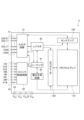
半導体記憶装置2の構成について説明する。図2に示されるように、半導体記憶装置2は、メモリセルアレイ110と、センスアンプ120と、ロウデコーダ130と、入出力回路21と、ロジック制御回路22と、シーケンサ41と、レジスタ42と、電圧生成回路43と、入出力用パッド群31と、ロジック制御用パッド群32と、電源入力用端子群33と、を備えている。
The configuration of the
メモリセルアレイ110は、データを記憶する部分である。図3には、メモリセルアレイ110の構成が等価回路図として示されている。メモリセルアレイ110は複数のブロックBLKにより構成されているのであるが、図3においては、これらのうちの1つのブロックBLKのみが図示されている。メモリセルアレイ110が有する他のブロックBLKの構成も、図3に示されるものと同じである。
図3に示されるように、ブロックBLKは、例えば4つのストリングユニットSU(SU0~SU3)を含む。また各々のストリングユニットSUは、複数のNANDストリングNSを含む。NANDストリングNSの各々は、例えば8個のメモリセルトランジスタMT(MT0~MT7)と、選択トランジスタST1、ST2とを含む。 As shown in FIG. 3, block BLK includes, for example, four string units SU (SU0 to SU3). Further, each string unit SU includes a plurality of NAND strings NS. Each NAND string NS includes, for example, eight memory cell transistors MT (MT0 to MT7) and selection transistors ST1 and ST2.
尚、メモリセルトランジスタMTの個数は8個に限られず、例えば、32個、48個、64個、96個でもよい。例えばカットオフ特性を高めるために、選択トランジスタST1、ST2のそれぞれが、単一ではなく複数のトランジスタにより構成されていてもよい。さらに、メモリセルトランジスタMTと選択トランジスタST1、ST2との間には、ダミーセルトランジスタが設けられていてもよい。 Note that the number of memory cell transistors MT is not limited to eight, and may be, for example, 32, 48, 64, or 96. For example, in order to improve cutoff characteristics, each of the selection transistors ST1 and ST2 may be composed of a plurality of transistors instead of a single transistor. Furthermore, a dummy cell transistor may be provided between the memory cell transistor MT and the selection transistors ST1 and ST2.
メモリセルトランジスタMTは、選択トランジスタST1と選択トランジスタST2との間において、直列接続されるようにして配置されている。一端側のメモリセルトランジスタMT7が、選択トランジスタST1のソースに接続され、他端側のメモリセルトランジスタMT0が、選択トランジスタST2のドレインに接続されている。 The memory cell transistor MT is arranged so as to be connected in series between the selection transistor ST1 and the selection transistor ST2. The memory cell transistor MT7 at one end is connected to the source of the selection transistor ST1, and the memory cell transistor MT0 at the other end is connected to the drain of the selection transistor ST2.
ストリングユニットSU0~SU3の各々の選択トランジスタST1のゲートは、それぞれセレクトゲート線SGD0~SGD3に共通接続されている。選択トランジスタST2のゲートは、同一のブロックBLK内にある複数のストリングユニットSU間で同一のセレクトゲート線SGSに共通接続されている。同一のブロックBLK内にあるメモリセルトランジスタMT0~MT7の制御ゲートは、それぞれワード線WL0~WL7に共通接続される。すなわち、ワード線WL0~WL7及びセレクトゲート線SGSは、同一ブロックBLK内の複数のストリングユニットSU0~SU3間で共通となっているのに対し、セレクトゲート線SGDは、同一ブロックBLK内であってもストリングユニットSU0~SU3毎に個別に設けられている。 The gates of the selection transistors ST1 of each of the string units SU0 to SU3 are commonly connected to select gate lines SGD0 to SGD3, respectively. The gates of the selection transistors ST2 are commonly connected to the same selection gate line SGS among a plurality of string units SU in the same block BLK. The control gates of memory cell transistors MT0 to MT7 in the same block BLK are commonly connected to word lines WL0 to WL7, respectively. That is, the word lines WL0 to WL7 and the select gate line SGS are common to multiple string units SU0 to SU3 within the same block BLK, whereas the select gate line SGD is common to multiple string units SU0 to SU3 within the same block BLK. are also provided individually for each string unit SU0 to SU3.
メモリセルアレイ110には、m本のビット線BL(BL0、BL1、・・・、BL(m-1))が設けられている。上記の「m」は、1つのストリングユニットSUに含まれるNANDストリングNSの本数を表す整数である。それぞれのNANDストリングNSのうち、選択トランジスタST1のドレインは、対応するビット線BLに接続されている。選択トランジスタST2のソースは、ソース線SLに接続されている。ソース線SLは、ブロックBLKが有する複数の選択トランジスタST2のソースに対し、共通接続されている。
The
同一のブロックBLK内にある複数のメモリセルトランジスタMTに記憶されているデータは、一括して消去される。一方、データの読み出し及び書き込みは、1つのワード線WLに接続され、且つ1つのストリングユニットSUに属する複数のメモリセルトランジスタMTに対して一括して行われる。それぞれのメモリセルは、上位ビット、中位ビット、及び下位ビットからなる3ビットのデータを保持することができる。 Data stored in a plurality of memory cell transistors MT in the same block BLK is erased all at once. On the other hand, reading and writing of data is performed at once on a plurality of memory cell transistors MT connected to one word line WL and belonging to one string unit SU. Each memory cell can hold 3-bit data consisting of an upper bit, a middle bit, and a lower bit.
つまり、本実施形態に係る半導体記憶装置2は、メモリセルトランジスタMTへのデータの書き込み方式として、1つのメモリセルトランジスタMTに3ビットデータを記憶させるTLC方式を採用している。このような態様に替えて、メモリセルトランジスタMTへのデータの書き込み方式としては、1つのメモリセルトランジスタMTに2ビットデータを記憶させるMLC方式や、1つのメモリセルトランジスタMTに1ビットデータを記憶させるSLC方式等を採用してもよい。
That is, the
尚、以下の説明では、1つのワード線WLに接続され、且つ1つのストリングユニットSUに属する複数のメモリセルトランジスタMTが記憶する1ビットデータの集合のことを「ページ」と称する。図3では、上記のような複数のメモリセルトランジスタMTからなる集合の一つに、符号「MG」が付してある。 In the following description, a set of 1-bit data stored in a plurality of memory cell transistors MT connected to one word line WL and belonging to one string unit SU will be referred to as a "page." In FIG. 3, one of the sets made up of the plurality of memory cell transistors MT as described above is labeled "MG".
本実施形態のように、1つのメモリセルトランジスタMTに3ビットのデータが記憶される場合、1つのストリングユニットSU内で共通のワード線WLに接続された複数のメモリセルトランジスタMTの集合は、3ページ分のデータを記憶することができる。 When 3 bits of data are stored in one memory cell transistor MT as in this embodiment, a set of a plurality of memory cell transistors MT connected to a common word line WL in one string unit SU is as follows: It can store three pages of data.
図4には、ビット線BLが伸びる方向に沿ってメモリセルアレイ110を切断した場合の断面が模式的に描かれている。同図に示されるように、メモリセルアレイ110では、ソース線層320の上に複数のNANDストリングNSが形成されている。ソース線層320は、埋め込みソース線(BSL)とも称されるものであり、図3のソース線SLに該当するものである。ソース線層320は例えばポリシリコンにより形成される。
FIG. 4 schematically shows a cross section of the
ソース線層320の上方には、セレクトゲート線SGSとして機能する複数の配線層333、ワード線WLとして機能する複数の配線層332、及びセレクトゲート線SGDとして機能する複数の配線層331が積層されている。これらはいずれも、互いに間隔を空けて上下に並ぶよう積層されている。積層された配線層333、332、331のそれぞれの間には、不図示の絶縁層が配置されている。本実施形態では、複数のワード線WLのそれぞれが、上記のように層状の配線層332として形成されている。配線層332は、本実施形態における「ワード線層」に該当する。
Above the
メモリセルアレイ110には複数のメモリホール334が形成されている。メモリホール334は、上記の配線層333、332、331、及びこれらの間にある不図示の絶縁層を上下方向に貫通しており、且つソース線層320に達する穴である。メモリホール334の側面には、ブロック絶縁膜335、電荷蓄積層336、及びゲート絶縁膜337が順次形成され、更にその内側に導電体柱338が埋め込まれている。導電体柱338は、例えばポリシリコンからなり、NANDストリングNSに含まれるメモリセルトランジスタMT並びに選択トランジスタST1及びST2の動作時にチャネルが形成される領域として機能する。このように、メモリホール334の内側には、ブロック絶縁膜335、電荷蓄積層336、ゲート絶縁膜337、及び導電体柱338からなる柱状体が形成されている。この柱状体のことを、以下では「メモリピラーMP」とも称する。メモリピラーMPは、配線層333、332、331を上下に貫通しており、その下端部はソース線層320に接続されている。
A plurality of
メモリホール334の内側に形成されたメモリピラーMPのうち、積層された配線層333、332、331のそれぞれと交差している各部分は、トランジスタとして機能する。これら複数のトランジスタのうち、配線層331と交差している部分にあるものは、選択トランジスタST1として機能する。複数のトランジスタのうち、配線層332と交差している部分にあるものは、メモリセルトランジスタMT(MT0~MT7)として機能する。複数のトランジスタのうち、配線層333と交差している部分にあるものは、選択トランジスタST2として機能する。このような構成により、各メモリホール334の内側に形成されたメモリピラーMPのそれぞれは、図3を参照しながら説明したNANDストリングNSとして機能する。メモリピラーMPの内側にある導電体柱338は、メモリセルトランジスタMTや選択トランジスタST1、ST2のチャンネルとして機能する部分である。
Of the memory pillar MP formed inside the
導電体柱338よりも上側には、ビット線BLとして機能する配線層が形成される。導電体柱338の上端には、導電体柱338とビット線BLとを接続するコンタクトプラグ339が形成されている。それぞれのビット線BLは、複数の配線層332等が積層されている方向とは交差する方向(図4では左右方向)に伸びる導体であって、上記のように、メモリピラーMPのうちソース線層320とは反対側の端部に対し、コンタクトプラグ339を介して接続されている。
A wiring layer functioning as a bit line BL is formed above the
図4に示される構成と同様の構成が、図4の紙面の奥行き方向に沿って複数配列されている。図4の紙面の奥行き方向に沿って一列に並ぶ複数のNANDストリングNSの集合によって、1つのストリングユニットSUが形成されている。 A plurality of configurations similar to the configuration shown in FIG. 4 are arranged along the depth direction of the paper surface of FIG. One string unit SU is formed by a collection of a plurality of NAND strings NS lined up in a row along the depth direction of the paper in FIG.
図4に示される複数のメモリピラーMPは、同一のブロックBLKに属している。メモリセルアレイ110に含まれるその他のブロックBLKは、図4に示されるブロックBLKの左右両側に配置されているのであるが、図4においてはその図示が省略されている。複数のブロックBLKの配置については、図9等を参照しながら後に説明する。
A plurality of memory pillars MP shown in FIG. 4 belong to the same block BLK. Other blocks BLK included in the
互いに隣り合うブロックBLKの間には、導体LIが配置されている。導体LIは、図4の紙面奥行き方向に沿って伸びる平板状に形成された導体であって、ブロックBLKの間を仕切るように配置されている。導体LIの下端はソース線層320に接続されている。導体LIの上端は不図示の配線層に接続されている。
A conductor LI is arranged between mutually adjacent blocks BLK. The conductor LI is a conductor formed in a flat plate shape extending along the depth direction of the plane of FIG. 4, and is arranged so as to partition between the blocks BLK. The lower end of conductor LI is connected to source
本実施形態に係る半導体記憶装置2では、ソース線層320と半導体基板300との間となる位置、すなわち、ソース線層320を挟んでメモリピラーMPとは反対側となる位置に、周辺回路PERが設けられている。周辺回路PERは、メモリセルトランジスタMTの動作を制御するための回路であって、メモリセルアレイ110におけるデータの書き込み動作や読み出し動作、及び消去動作等を実現するものである。図2に示されるセンスアンプ120、ロウデコーダ130、及び電圧生成回路43等は、周辺回路PERの一部となっている。周辺回路PERは、各種のトランジスタやRC回路等を含んでいる。図4に示される例では、半導体基板300上に形成されたトランジスタTRと、メモリセルアレイ110の上方側にあるビット線BLとの間が、コンタクト924を介して電気的に接続されている。
In the
尚、このような構成に換えて、半導体基板300の上に直接メモリセルアレイ110が設けられている構成としてもよい。この場合、半導体基板300のp型ウェル領域が、ソース線SLすなわちソース線層として機能することとなる。また、周辺回路PERは、半導体基板300の表面に沿ってメモリセルアレイ110と隣り合う位置に設けられることとなる。
Note that instead of this configuration, a configuration in which the
図2に戻って説明を続ける。センスアンプ120は、ビット線BLに印加される電圧を調整したり、ビット線BLの電圧を読み出してデータに変換したりするための回路である。センスアンプ120は、データの読み出し時には、メモリセルトランジスタMTからビット線BLに読み出された読み出しデータを取得し、取得した読み出しデータを入出力回路21に転送する。センスアンプ120は、データの書き込み時には、ビット線BLを介して書き込まれる書き込みデータをメモリセルトランジスタMTに転送する。センスアンプ120の動作は、後述のシーケンサ41により制御される。
Returning to FIG. 2, the explanation will be continued. The
センスアンプ120は、複数のビット線BLのそれぞれ対応した複数のセンスアンプユニットSAUを含んでいる。1つのビット線BLには、1つのセンスアンプユニットSAUが接続されている。つまり、センスアンプユニットSAUは、ストリングユニットSUのメモリセルトランジスタMTに対しビット線BLを介して接続された回路、ということができる。図5には、1つのセンスアンプユニットSAUの詳細な回路構成が抽出して示されている。
The
図5に示されるように、センスアンプユニットSAUは、センスアンプ部SAと、ラッチ回路SDL、ADL、BDL、CDL、XDLとを含んでいる。センスアンプ部SA、ラッチ回路SDL、ADL、BDL、CDL、XDLは、互いにデータを送受信可能なように、バスLBUSによって接続されている。 As shown in FIG. 5, the sense amplifier unit SAU includes a sense amplifier section SA and latch circuits SDL, ADL, BDL, CDL, and XDL. The sense amplifier section SA and the latch circuits SDL, ADL, BDL, CDL, and XDL are connected by a bus LBUS so that they can send and receive data to and from each other.
センスアンプ部SAは、例えば読み出し動作において、対応するビット線BLに読み出されたデータをセンスして、読み出したデータが“0”であるか“1”であるかを判定する。センスアンプ部SAは、例えば、pチャネルMOSトランジスタであるトランジスタTR1と、nチャネルMOSトランジスタであるトランジスタTR2~TR9と、キャパシタC10とを含んでいる。 For example, in a read operation, the sense amplifier section SA senses the data read to the corresponding bit line BL and determines whether the read data is "0" or "1". The sense amplifier section SA includes, for example, a transistor TR1 which is a p-channel MOS transistor, transistors TR2 to TR9 which are n-channel MOS transistors, and a capacitor C10.
トランジスタTR1の一端は電源線に接続されており、トランジスタTR1の他端はトランジスタTR2に接続されている。トランジスタTR1のゲートは、ラッチ回路SDL内のノードINV_Sに接続されている。トランジスタTR2の一端はトランジスタTR1に接続されており、トランジスタTR2の他端はノードCOMに接続されている。トランジスタTR2のゲートには信号BLXが入力される。トランジスタTR3の一端はノードCOMに接続されており、トランジスタTR3の他端はトランジスタTR4に接続されている。トランジスタTR3のゲートには信号BLCが入力される。トランジスタTR4は、高耐圧のMOSトランジスタである。トランジスタTR4の一端はトランジスタTR3に接続されている。トランジスタTR4の他端は対応するビット線BLに接続されている。トランジスタTR4のゲートには信号BLSが入力される。 One end of the transistor TR1 is connected to a power supply line, and the other end of the transistor TR1 is connected to a transistor TR2. The gate of transistor TR1 is connected to node INV_S in latch circuit SDL. One end of the transistor TR2 is connected to the transistor TR1, and the other end of the transistor TR2 is connected to the node COM. A signal BLX is input to the gate of the transistor TR2. One end of the transistor TR3 is connected to the node COM, and the other end of the transistor TR3 is connected to the transistor TR4. A signal BLC is input to the gate of the transistor TR3. The transistor TR4 is a high voltage MOS transistor. One end of the transistor TR4 is connected to the transistor TR3. The other end of the transistor TR4 is connected to the corresponding bit line BL. A signal BLS is input to the gate of the transistor TR4.
トランジスタTR5の一端はノードCOMに接続されており、トランジスタTR5の他端はノードSRCに接続されている。トランジスタTR5のゲートはノードINV_Sに接続されている。トランジスタTR6の一端は、トランジスタTR1とトランジスタTR2との間に接続されており、トランジスタTR6の他端はノードSENに接続されている。トランジスタTR6のゲートには信号HLLが入力される。トランジスタTR7の一端はノードSENに接続されており、トランジスタTR7の他端はノードCOMに接続されている。トランジスタTR7のゲートには信号XXLが入力される。 One end of the transistor TR5 is connected to the node COM, and the other end of the transistor TR5 is connected to the node SRC. The gate of transistor TR5 is connected to node INV_S. One end of the transistor TR6 is connected between the transistor TR1 and the transistor TR2, and the other end of the transistor TR6 is connected to the node SEN. A signal HLL is input to the gate of the transistor TR6. One end of the transistor TR7 is connected to the node SEN, and the other end of the transistor TR7 is connected to the node COM. A signal XXL is input to the gate of the transistor TR7.
トランジスタTR8の一端は接地されており、トランジスタTR8の他端はトランジスタTR9に接続されている。トランジスタTR8のゲートはノードSENに接続されている。トランジスタTR9の一端はトランジスタTR8に接続されており、トランジスタTR9の他端はバスLBUSに接続されている。トランジスタTR9のゲートには信号STBが入力される。キャパシタC10の一端はノードSENに接続されている。キャパシタC10の他端にはクロックCLKが入力される。 One end of the transistor TR8 is grounded, and the other end of the transistor TR8 is connected to the transistor TR9. The gate of transistor TR8 is connected to node SEN. One end of the transistor TR9 is connected to the transistor TR8, and the other end of the transistor TR9 is connected to the bus LBUS. A signal STB is input to the gate of the transistor TR9. One end of capacitor C10 is connected to node SEN. A clock CLK is input to the other end of the capacitor C10.
信号SW、BLX、BLC、BLS、HLL、XXL、及びSTBは、例えばシーケンサ41によって生成される。また、トランジスタTR1の一端に接続された電源線には、例えば半導体記憶装置2の内部電源電圧である電圧Vddが印加され、ノードSRCには、例えば半導体記憶装置2の接地電圧である電圧Vssが印加される。
The signals SW, BLX, BLC, BLS, HLL, XXL, and STB are generated by the
ラッチ回路SDL、ADL、BDL、CDL、XDLは、読み出しデータや書き込みデータを一時的に保持する。ラッチ回路XDLは入出力回路21に接続され、センスアンプユニットSAUと入出力回路21との間のデータの入出力に使用される。
The latch circuits SDL, ADL, BDL, CDL, and XDL temporarily hold read data and write data. The latch circuit XDL is connected to the input/
ラッチ回路SDLは、例えば、インバータIV11、IV12と、nチャネルMOSトランジスタであるトランジスタTR13、TR14とを含んでいる。インバータIV11の入力ノードはノードLAT_Sに接続されている。インバータIV11の出力ノードはノードINV_Sに接続されている。インバータIV12の入力ノードはノードINV_Sに接続されている。インバータIV12の出力ノードはノードLAT_Sに接続されている。トランジスタTR13の一端はノードINV_Sに接続されており、トランジスタTR13の他端はバスLBUSに接続されている。トランジスタTR13のゲートには信号STI_Sが入力される。トランジスタTR13の一端はノードLAT_Sに接続されており、トランジスタTR14の他端はバスLBUSに接続されている。トランジスタTR14のゲートには信号STL_Sが入力される。例えば、ノードLAT_Sにおいて保持されるデータがラッチ回路SDLに保持されるデータに相当する。また、ノードINV_Sにおいて保持されるデータは、ノードLAT_Sに保持されるデータの反転データに相当する。ラッチ回路ADL、BDL、CDL、XDLの回路構成は、例えば、ラッチ回路SDLの回路構成と同様のため、説明を省略する。 The latch circuit SDL includes, for example, inverters IV11 and IV12, and transistors TR13 and TR14, which are n-channel MOS transistors. The input node of inverter IV11 is connected to node LAT_S. The output node of inverter IV11 is connected to node INV_S. The input node of inverter IV12 is connected to node INV_S. The output node of inverter IV12 is connected to node LAT_S. One end of the transistor TR13 is connected to the node INV_S, and the other end of the transistor TR13 is connected to the bus LBUS. A signal STI_S is input to the gate of the transistor TR13. One end of the transistor TR13 is connected to the node LAT_S, and the other end of the transistor TR14 is connected to the bus LBUS. A signal STL_S is input to the gate of the transistor TR14. For example, data held at node LAT_S corresponds to data held in latch circuit SDL. Further, the data held at the node INV_S corresponds to the inverted data of the data held at the node LAT_S. The circuit configurations of the latch circuits ADL, BDL, CDL, and XDL are similar to, for example, the circuit configuration of the latch circuit SDL, and therefore the description thereof will be omitted.
図2に戻って説明を続ける。ロウデコーダ130は、ワード線WLのそれぞれに電圧を印加するための、不図示のスイッチ群として構成された回路である。ロウデコーダ130は、レジスタ42からブロックアドレス及びロウアドレスを受け取り、当該ブロックアドレスに基づいて対応するブロックBLKを選択するとともに、当該ロウアドレスに基づいて対応するワード線WLを選択する。ロウデコーダ130は、選択されたワード線WLに対して電圧生成回路43からの電圧が印加されるよう、上記のスイッチ群の開閉を切り換える。ロウデコーダ130の動作はシーケンサ41により制御される。
Returning to FIG. 2, the explanation will be continued. The
入出力回路21は、メモリコントローラ1との間で、信号DQ<7:0>、及び、データストローブ信号DQS、/DQSを送受信する。入出力回路21は、信号DQ<7:0>内のコマンド及びアドレスをレジスタ42に転送する。また、入出力回路21は、書き込みデータ及び読み出しデータを、センスアンプ120との間で送受信する。
The input/
ロジック制御回路22は、メモリコントローラ1からチップイネーブル信号/CE、コマンドラッチイネーブル信号CLE、アドレスラッチイネーブル信号ALE、ライトイネーブル信号/WE、リードイネーブル信号RE、/RE、及びライトプロテクト信号/WPを受信する。また、ロジック制御回路22は、レディービジー信号R/Bをメモリコントローラ1に転送して、半導体記憶装置2の状態を外部に通知する。
The
シーケンサ41は、メモリコントローラ1からインターフェイス回路20へと入力された制御信号に基づいて、メモリセルアレイ110を含む各部の動作を制御する。シーケンサ41は、半導体記憶装置10の全体の動作を統括する「制御回路」として機能するものである。
The
レジスタ42は、コマンドやアドレスを一時的に保持する部分である。レジスタ42には、書き込み動作や読み出し動作、及び消去動作等を指示するコマンドが保持される。当該コマンドは、メモリコントローラ1から入出力回路21に入力された後、入出力回路21からレジスタ42に転送され保持される。
The
また、レジスタ42は、上記のコマンドに対応するアドレスも保持される。当該アドレスは、メモリコントローラ1から入出力回路21に入力された後、入出力回路21からレジスタ42に転送され保持される。
The
更に、レジスタ42は、半導体記憶装置2の動作状態を示すステータス情報も保持される。ステータス情報は、メモリセルアレイ110等の動作状態に応じて、シーケンサ41によって都度更新される。ステータス情報は、メモリコントローラ1からの要求に応じて、状態信号として入出力回路21からメモリコントローラ1へと出力される。
Furthermore, the
電圧生成回路43は、メモリセルアレイ110におけるデータの書き込み動作、読み出し動作、及び、消去動作のそれぞれに必要な電圧を生成する部分である。このような電圧には、例えば、それぞれのワード線WLに印加される電圧や、それぞれのビット線BLに印加される電圧等が含まれる。電圧生成回路43の動作はシーケンサ41によって制御される。
The
入出力用パッド群31は、メモリコントローラ1と入出力回路21との間で各信号の送受信を行うための、複数の端子(パッド)が設けられた部分である。それぞれの端子は、信号DQ<7:0>、及び、データストローブ信号DQS、/DQSのそれぞれに対応して個別に設けられている。
The input/
ロジック制御用パッド群32は、メモリコントローラ1とロジック制御回路22との間で各信号の送受信を行うための、複数の端子(パッド)が設けられた部分である。それぞれの端子は、チップイネーブル信号/CE、コマンドラッチイネーブル信号CLE、アドレスラッチイネーブル信号ALE、ライトイネーブル信号/WE、リードイネーブル信号RE、/RE、ライトプロテクト信号/WP、及び、レディービジー信号R/Bのそれぞれに対応して個別に設けられている。
The logic
電源入力用端子群33は、半導体記憶装置2の動作に必要な各電圧の印加を受けるための、複数の端子が設けられた部分である。それぞれの端子に印加される電圧には、電源電圧Vcc、VccQ、Vpp、及び接地電圧Vssが含まれる。
The power
電源電圧Vccは、動作電源として外部から与えられる回路電源電圧であり、例えば3.3V程度の電圧である。電源電圧VccQは、例えば1.2Vの電圧である。電源電圧VccQは、メモリコントローラ1と半導体記憶装置2との間で信号を送受信する際に用いられる電圧である。電源電圧Vppは、電源電圧Vccよりも高圧の電源電圧であり、例えば12Vの電圧である。
The power supply voltage Vcc is a circuit power supply voltage applied from the outside as an operating power supply, and is, for example, a voltage of about 3.3V. Power supply voltage VccQ is, for example, a voltage of 1.2V. Power supply voltage VccQ is a voltage used when transmitting and receiving signals between
メモリセルアレイ110へデータを書き込んだり、データを消去したりする際には、20V程度の高い電圧が必要となる。この際に、約3.3Vの電源電圧Vccを電圧生成回路43の昇圧回路で昇圧するよりも、約12Vの電源電圧Vppを昇圧するほうが、高速且つ低消費電力で所望の電圧を生成することができる。一方で、例えば、高電圧を供給することができない環境において半導体記憶装置2が用いられる場合、電源電圧Vppには電圧が供給されなくともよい。電源電圧Vppが供給されない場合であっても、半導体記憶装置2は、電源電圧Vccが供給されていれば、各種の動作を実行することができる。すなわち、電源電圧Vccは、半導体記憶装置2に標準的に供給される電源であり、電源電圧Vppは、例えば使用環境に応じて追加的・任意的に供給される電源である。
When writing data to or erasing data from the
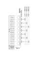
図6は、メモリセルトランジスタMTの閾値分布等を模式的に示す図である。図6の中段にある図は、メモリセルトランジスタMTの閾値電圧(横軸)と、メモリセルトランジスタMTの個数(縦軸)との対応関係を表している。 FIG. 6 is a diagram schematically showing the threshold distribution and the like of the memory cell transistor MT. The diagram in the middle of FIG. 6 shows the correspondence between the threshold voltage of the memory cell transistor MT (horizontal axis) and the number of memory cell transistors MT (vertical axis).
本実施形態のようにTLC方式を採用した場合においては、複数のメモリセルトランジスタMTは、図6の中段に示されるように、8つの閾値分布を形成する。この8個の閾値分布(書き込みレベル)のことを、閾値電圧の低い方から順に“ER”レベル、“A”レベル、“B”レベル、“C”レベル、“D”レベル、“E”レベル、“F”レベル、“G”レベルと称する。 When the TLC method is adopted as in this embodiment, the plurality of memory cell transistors MT form eight threshold distributions, as shown in the middle part of FIG. These eight threshold distributions (write levels) are defined as "ER" level, "A" level, "B" level, "C" level, "D" level, and "E" level in order from the lowest threshold voltage. , "F" level, and "G" level.
図6の上段にある表は、閾値電圧の上記各レベルのそれぞれに対応して、割り当てられるデータの例を表している。同表に示されるように、“ER”レベル、“A”レベル、“B”レベル、“C”レベル、“D”レベル、“E”レベル、“F”レベル、及び“G”レベルには、例えば以下に示すような、それぞれ異なる3ビットデータが割り当てられている。
“ER”レベル:“111”(“下位ビット/中位ビット/上位ビット”)
“A”レベル:“011”
“B”レベル:“001”
“C”レベル:“000”
“D”レベル:“010”
“E”レベル:“110”
“F”レベル:“100”
“G”レベル:“101”
The table in the upper part of FIG. 6 shows examples of data allocated to each of the above-mentioned levels of threshold voltage. As shown in the table, the "ER" level, "A" level, "B" level, "C" level, "D" level, "E" level, "F" level, and "G" level are , for example, different 3-bit data as shown below are assigned.
“ER” level: “111” (“lower bit/middle bit/upper bit”)
“A” level: “011”
“B” level: “001”
“C” level: “000”
“D” level: “010”
“E” level: “110”
“F” level: “100”
“G” level: “101”
互いに隣り合う一対の閾値分布の間には、それぞれ書き込み動作で使用されるベリファイ電圧が設定される。具体的には、“A”レベル、“B”レベル、“C”レベル、“D”レベル、“E”レベル、“F”レベル、及び“G”レベルにそれぞれ対応して、ベリファイ電圧VfyA、VfyB、VfyC、VfyD、VfyE、VfyF、及びVfyGが設定される。 A verify voltage used in a write operation is set between a pair of threshold distributions adjacent to each other. Specifically, the verify voltages VfyA, VfyB, VfyC, VfyD, VfyE, VfyF, and VfyG are set.
ベリファイ電圧VfyAは、“ER”レベルにおける最大の閾値電圧と“A”レベルにおける最小の閾値電圧との間に設定される。ワード線WLにベリファイ電圧VfyAが印加されると、当該ワード線WLに繋がるメモリセルトランジスタMTのうち、閾値電圧が“ER”レベルに含まれるメモリセルトランジスタMTがオン状態になり、閾値電圧が“A”レベル以上の閾値分布に含まれるメモリセルトランジスタMTがオフ状態になる。 The verify voltage VfyA is set between the maximum threshold voltage at the "ER" level and the minimum threshold voltage at the "A" level. When the verify voltage VfyA is applied to the word line WL, among the memory cell transistors MT connected to the word line WL, the memory cell transistors MT whose threshold voltages are included in the "ER" level are turned on, and the threshold voltages become " Memory cell transistors MT included in the threshold distribution of level A'' or higher are turned off.
その他のベリファイ電圧VfyB、VfyC、VfyD、VfyE、VfyF、及びVfyGも、上記のベリファイ電圧VfyAと同様に設定される。ベリファイ電圧VfyBは、“A”レベルと“B”レベルとの間に設定され、ベリファイ電圧VfyCは、“B”レベルと“C”レベルとの間に設定され、ベリファイ電圧VfyDは、“C”レベルと“D”レベルとの間に設定され、ベリファイ電圧VfyEは、“D”レベルと“E”レベルとの間に設定され、ベリファイ電圧VfyFは、“E”レベルと“F”レベルとの間に設定され、ベリファイ電圧VfyGは、“F”レベルと“G”レベルとの間に設定される。 Other verify voltages VfyB, VfyC, VfyD, VfyE, VfyF, and VfyG are also set in the same manner as the above verify voltage VfyA. Verify voltage VfyB is set between "A" level and "B" level, verify voltage VfyC is set between "B" level and "C" level, and verify voltage VfyD is set between "C" level. The verify voltage VfyE is set between the "D" level and the "D" level, and the verify voltage VfyF is set between the "E" level and the "F" level. The verify voltage VfyG is set between the "F" level and the "G" level.
例えば、ベリファイ電圧VfyAは0.8Vに、ベリファイ電圧VfyBは1.6Vに、ベリファイ電圧VfyCは2.4Vに、ベリファイ電圧VfyDは3.1Vに、ベリファイ電圧VfyEは3.8Vに、ベリファイ電圧VfyFは4.6Vに、ベリファイ電圧VfyGは5.6Vに、それぞれ設定してもよい。しかし、これに限定されることなく、ベリファイ電圧VfyA、VfyB、VfyC、VfyD、VfyE、VfyF、及びVfyGは、例えば、0V~7.0Vの範囲で、適宜、段階的に設定してもよい。 For example, verify voltage VfyA is 0.8V, verify voltage VfyB is 1.6V, verify voltage VfyC is 2.4V, verify voltage VfyD is 3.1V, verify voltage VfyE is 3.8V, verify voltage VfyF may be set to 4.6V, and the verify voltage VfyG may be set to 5.6V. However, the present invention is not limited thereto, and the verify voltages VfyA, VfyB, VfyC, VfyD, VfyE, VfyF, and VfyG may be set stepwise as appropriate within the range of 0V to 7.0V, for example.
また、隣り合う閾値分布の間には、それぞれ読み出し動作で使用される読み出し電圧が設定される。「読み出し電圧」とは、読み出し動作時において、読み出し対象となるメモリセルトランジスタMTに繋がるワード線WL、すなわち選択ワード線に対し印加される電圧である。読み出し動作では、読み出し対象となるメモリセルトランジスタMTの閾値電圧が、印加された読み出し電圧よりも高いか否かの判定結果に基づいてデータが決定される。 Furthermore, read voltages used in read operations are set between adjacent threshold distributions. The "read voltage" is a voltage applied to the word line WL connected to the memory cell transistor MT to be read, that is, the selected word line, during a read operation. In the read operation, data is determined based on a determination result of whether the threshold voltage of the memory cell transistor MT to be read is higher than the applied read voltage.
図6の下段の図において模式的に示されるように、具体的には、メモリセルトランジスタMTの閾値電圧が“ER”レベルに含まれるのか“A”レベル以上に含まれるのかを判定する読み出し電圧VrAは、“ER”レベルにおける最大の閾値電圧と“A”レベルにおける最小の閾値電圧との間に設定される。 As schematically shown in the lower diagram of FIG. 6, specifically, the read voltage for determining whether the threshold voltage of the memory cell transistor MT is included in the "ER" level or higher than the "A" level VrA is set between the maximum threshold voltage at the "ER" level and the minimum threshold voltage at the "A" level.
その他の読み出し電圧VrB、VrC、VrD、VrE、VrF、及びVrGも、上記の読み出し電圧VrAと同様に設定される。読み出し電圧VrBは、“A”レベルと“B”レベルとの間に設定され、読み出し電圧VrCは、“B”レベルと“C”レベルとの間に設定され、読み出し電圧VrDは、“C”レベルと“D”レベルとの間に設定され、読み出し電圧VrEは、“D”レベルと“E”レベルとの間に設定され、読み出し電圧VrFは、“E”レベルと“F”レベルとの間に設定され、読み出し電圧VrGは、“F”レベルと“G”レベルとの間に設定される。 The other read voltages VrB, VrC, VrD, VrE, VrF, and VrG are also set in the same way as the above read voltage VrA. Read voltage VrB is set between "A" level and "B" level, read voltage VrC is set between "B" level and "C" level, and read voltage VrD is set between "C" level. The read voltage VrE is set between the "D" level and the "D" level, and the read voltage VrF is set between the "E" level and the "F" level. The read voltage VrG is set between the "F" level and the "G" level.
そして、最も高い閾値分布(例えば“G”レベル)の最大の閾値電圧よりも高い電圧に、読み出しパス電圧VPASS_READが設定される。読み出しパス電圧VPASS_READがゲートに印加されたメモリセルトランジスタMTは、記憶するデータに依らずにオン状態になる。 Then, the read pass voltage VPASS_READ is set to a voltage higher than the maximum threshold voltage of the highest threshold distribution (for example, "G" level). The memory cell transistor MT to which the read pass voltage VPASS_READ is applied to its gate is turned on regardless of the data to be stored.
尚、ベリファイ電圧VfyA、VfyB、VfyC、VfyD、VfyE、VfyF、及びVfyGは、例えば、読み出し電圧VrA、VrB、VrC、VrD、VrE、VrF、及びVrGよりもそれぞれ高い電圧に設定される。つまり、ベリファイ電圧VfyA、VfyB、VfyC、VfyD、VfyE、VfyF、及びVfyGは、それぞれ“A”レベル、“B”レベル、“C”レベル、“D”レベル、“E”レベル、“F”レベル、及び“G”レベルの閾値分布の下裾近傍に設定される。 Note that the verify voltages VfyA, VfyB, VfyC, VfyD, VfyE, VfyF, and VfyG are set to higher voltages than the read voltages VrA, VrB, VrC, VrD, VrE, VrF, and VrG, respectively, for example. In other words, the verify voltages VfyA, VfyB, VfyC, VfyD, VfyE, VfyF, and VfyG are "A" level, "B" level, "C" level, "D" level, "E" level, and "F" level, respectively. , and near the lower tail of the "G" level threshold distribution.
以上に説明したようなデータの割り付けが適用された場合、読み出し動作において下位ビットの1ページデータ(下位ページデータ)は、読み出し電圧VrA及びVrEを用いた読み出し結果によって確定させることができる。中位ビットの1ページデータ(中位ページデータ)は、読み出し電圧VrB、VrD、及びVrFを用いた読み出し結果によって確定させることができる。上位ビットの1ページデータ(上位ページデータ)は、読み出し電圧VrC及びVrGを用いた読み出し結果によって確定させることができる。このように、下位ページデータ、中位ページデータ、及び上位ページデータがそれぞれ、2回、3回、及び2回の読み出し動作によって確定するため、以上のようなデータの割り付けは“2-3-2コード”と称される。 When the data allocation as described above is applied, one page data (lower page data) of lower bits in a read operation can be determined by the read result using read voltages VrA and VrE. One page data of middle bits (middle page data) can be determined by the read result using read voltages VrB, VrD, and VrF. One page data (upper page data) of upper bits can be determined by the read result using read voltages VrC and VrG. In this way, since the lower page data, middle page data, and upper page data are determined by two, three, and two read operations, respectively, the above data allocation is performed as follows. 2 code".
尚、以上で説明したようなデータの割り付けはあくまで一例であり、実際のデータの割り付けはこれに限定されない。例えば、2ビット又は4ビット以上のデータが1つのメモリセルトランジスタMTに記憶されてもよい。また、データが割り付けられる閾値分布の数は7以下であってもよく、9以上であってもよい。例えば、“2-3-2コード”に代えて、“1-3-3コード”又は“1-2-4コード”を用いてもよい。また、例えば、下位ビット/中位ビット/上位ビットの割り当てを変更してもよい。より具体的には、例えば、“2-3-2コード”において、下位ページデータを読み出し電圧VrC及びVrBを用いた読み出し結果によって確定させ、中位ページデータを読み出し電圧VrB、VrD、及びVrFを用いた読み出し結果によって確定させ、上位ページデータを読み出し電圧VrA及びVrEを用いた読み出し結果によって確定させるようにデータを割り当ててもよい。すなわち、例えば、下位ビットと上位ビットの割り当てを入れ替えてもよい。この場合、閾値電圧の各レベルのそれぞれに対応して、以下のようにデータが割り当てられる。
“ER”レベル:“111”(“下位ビット/中位ビット/上位ビット”)
“A”レベル:“110”
“B”レベル:“100”
“C”レベル:“000”
“D”レベル:“010”
“E”レベル:“011”
“F”レベル:“001”
“G”レベル:“101”
Note that the data allocation as described above is just an example, and the actual data allocation is not limited to this. For example, 2 bits or 4 bits or more of data may be stored in one memory cell transistor MT. Further, the number of threshold distributions to which data is allocated may be 7 or less, or may be 9 or more. For example, instead of the "2-3-2 code", a "1-3-3 code" or a "1-2-4 code" may be used. Furthermore, for example, the allocation of lower bits/middle bits/upper bits may be changed. More specifically, for example, in the "2-3-2 code", lower page data is determined by the read result using read voltages VrC and VrB, and middle page data is determined by read voltages VrB, VrD, and VrF. Data may be allocated such that the upper page data is determined by the read result using the read voltages VrA and VrE. That is, for example, the allocation of lower bits and upper bits may be exchanged. In this case, data is allocated as follows, corresponding to each level of threshold voltage.
“ER” level: “111” (“lower bit/middle bit/upper bit”)
“A” level: “110”
“B” level: “100”
“C” level: “000”
“D” level: “010”
“E” level: “011”
“F” level: “001”
“G” level: “101”
半導体記憶装置2において行われる書き込み動作について説明する。書き込み動作では、プログラム動作及びベリファイ動作が行われる。「プログラム動作」とは、一部のメモリセルトランジスタMTの電荷蓄積層336に電子を注入することにより、当該メモリセルトランジスタMTの閾値電圧を変化させる動作のことである。「ベリファイ動作」とは、上記のプログラム動作の後、データを読み出すことで、メモリセルトランジスタMTの閾値電圧がターゲットレベルまで達したか否かを判定し検証する動作である。閾値電圧がターゲットレベルまで達したメモリセルトランジスタMTは、その後、書き込み禁止とされる。
A write operation performed in the
書き込み動作では、以上のプログラム動作及びベリファイ動作が繰り返し実行される。これにより、メモリセルトランジスタMTの閾値電圧がターゲットレベルまで上昇する。 In the write operation, the above program operation and verify operation are repeatedly executed. This increases the threshold voltage of memory cell transistor MT to the target level.
複数のワード線WLのうち、書き込み動作の対象(つまり、閾値電圧を変化させる対象)であるメモリセルトランジスタMTに繋がっているワード線WLのことを、以下では「選択ワード線」とも称する。また、書き込み動作の対象ではないメモリセルトランジスタMTに繋がっているワード線WLのことを、以下では「非選択ワード線」とも称する。 Among the plurality of word lines WL, the word line WL connected to the memory cell transistor MT that is the target of the write operation (that is, the target of changing the threshold voltage) is also referred to as a "selected word line" below. Further, the word line WL connected to the memory cell transistor MT that is not the target of the write operation is also referred to as an "unselected word line" below.
複数のストリングユニットSUのうち、書き込み動作の対象となるストリングユニットSUのことを、以下では「選択ストリングユニット」とも称する。また、書き込み動作の対象とはならないストリングユニットSUのことを、以下では「非選択ストリングユニット」とも称する。 Among the plurality of string units SU, the string unit SU that is the target of the write operation is also referred to as a "selected string unit" below. In addition, the string units SU that are not targets of the write operation are also referred to as "unselected string units" below.
プログラム動作について説明する。図7は、プログラム動作時における各配線の電位変化を示している。プログラム動作では、センスアンプ120が、プログラムデータに対応して各ビット線BLの電位を変化させる。プログラム対象の(閾値電圧を上昇させるべき)メモリセルトランジスタMTに繋がるビット線BLには、“L”レベルとして例えば接地電圧Vss(0V)が印加される。プログラム対象ではない(閾値電圧を維持させるべき)メモリセルトランジスタMTに繋がるビット線BLには、“H”レベルとして、例えば2.5Vが印加される。前者のビット線BLは、図7においては「BL(0)」と表記されている。後者のビット線BLは、図7においては「BL(1)」と表記されている。
The program operation will be explained. FIG. 7 shows potential changes of each wiring during a program operation. In the program operation, the
ロウデコーダ130は、書き込み動作の対象としていずれかのブロックBLKを選択し、更にいずれかのストリングユニットSUを選択する。より具体的には、選択されたストリングユニットSUにおけるセレクトゲート線SGD(選択セレクトゲート線SGDsel)には、電圧生成回路43からロウデコーダ130を介して例えば5Vが印加される。これにより、選択トランジスタST1はオン状態となる。他方で、セレクトゲート線SGSには、電圧生成回路43からロウデコーダ130を介して例えば電圧Vssが印加される。これにより、選択トランジスタST2はオフ状態となる。
The
また、選択ブロックBLKにおける非選択ストリングユニットSUのセレクトゲート線SGD(非選択セレクトゲート線SGDusel)には、電圧生成回路43からロウデコーダ130を介して例えば電圧5Vが印加される。これにより、選択トランジスタST1がオン状態となる。なお、各ブロックBLKに含まれるストリングユニットSUにおいて、セレクトゲート線SGSは共通に接続されている。従って、非選択ストリングユニットSUにおいても、選択トランジスタST2はオフ状態となる。
Furthermore, a voltage of 5 V, for example, is applied from the
更に、非選択ブロックBLKにおけるセレクトゲート線SGD及びセレクトゲート線SGSには、電圧生成回路43からロウデコーダ130を介して例えば電圧Vssが印加される。これにより、選択トランジスタST1及び選択トランジスタST2はオフ状態となる。
Furthermore, a voltage Vss, for example, is applied from the
ソース線SLは、セレクトゲート線SGSの電位よりも高い電位とされる。当該電位は、例えば1Vである。 The source line SL is set to a higher potential than the select gate line SGS. The potential is, for example, 1V.
その後、選択ブロックBLKにおける選択セレクトゲート線SGDselの電位を、例えば2.5Vとする。この電位は、上記の例で0Vが与えられたビット線BL(0)に対応する選択トランジスタST1はオンさせるが、2.5Vが与えられたビット線BL(1)に対応する選択トランジスタST1はカットオフさせる電圧である。これにより、選択ストリングユニットSUにおいては、ビット線BL(0)に対応する選択トランジスタST1はオンされ、2.5Vが与えられたビット線BL(1)に対応する選択トランジスタST1はカットオフされる。一方で、非選択セレクトゲート線SGDuselの電位を、例えば電圧Vssとする。これにより、非選択ストリングユニットSUにおいては、ビット線BL(0)及びビット線BL(1)の電位に関わらず、選択トランジスタST1はカットオフされる。 Thereafter, the potential of the selected select gate line SGDsel in the selected block BLK is set to 2.5V, for example. This potential turns on the selection transistor ST1 corresponding to the bit line BL(0) to which 0V is applied in the above example, but the selection transistor ST1 corresponding to the bit line BL(1) to which 2.5V is applied turns on. This is the voltage to be cut off. As a result, in the selected string unit SU, the selection transistor ST1 corresponding to the bit line BL(0) is turned on, and the selection transistor ST1 corresponding to the bit line BL(1) to which 2.5V is applied is cut off. . On the other hand, the potential of the unselected select gate line SGDusel is set to, for example, voltage Vss. As a result, in the unselected string unit SU, the selection transistor ST1 is cut off regardless of the potentials of the bit line BL(0) and bit line BL(1).
そしてロウデコーダ130は、選択ブロックBLKにおいて、書き込み動作の対象としていずれかのワード線WLを選択する。書き込み動作の対象となるワード線WL(選択ワード線WLsel)に、電圧生成回路43からロウデコーダ130を介して例えば電圧VPGMが印加される。一方で、その他のワード線WL(非選択ワード線WLusel)に、電圧生成回路43からロウデコーダ130を介して例えば電圧VPASS_PGMが印加される。電圧VPGMは、トンネル現象により電子を電荷蓄積層336に注入するための高電圧である。電圧VPASS_PGMは、ワード線WLに繋がるメモリセルトランジスタMTをONとする一方で、閾定電圧は変化させない程度の電圧である。VPGMはVPASS_PGMよりも高い電圧である。
The
プログラム対象のビット線BL(0)に対応するNANDストリングNSでは、選択トランジスタST1がオン状態となる。そのため、選択ワード線WLselに接続されたメモリセルトランジスタMTのチャネル電位は0Vとなる。制御ゲートとチャネルとの間の電位差が大きくなり、その結果、電子が電荷蓄積層336に注入されるので、メモリセルトランジスタMTの閾値電圧が上昇される。
In the NAND string NS corresponding to the bit line BL(0) to be programmed, the selection transistor ST1 is turned on. Therefore, the channel potential of the memory cell transistor MT connected to the selected word line WLsel becomes 0V. The potential difference between the control gate and the channel increases, and as a result, electrons are injected into the
プログラム対象ではないビット線BL(1)に対応するNANDストリングNSでは、選択トランジスタST1がカットオフ状態となる。そのため、選択ワード線WLselに接続されたメモリセルトランジスタMTのチャネルは電気的にフローティングとなり、ワード線WL等との容量カップリングによりチャネル電位は電圧VPGM近くまで上昇される。制御ゲートとチャネルとの間の電位差が小さくなり、その結果、電子は電荷蓄積層336に注入されないので、メモリセルトランジスタMTの閾値電圧は維持される。正確にいうと、閾値分布レベルがより高い分布に遷移するほどには、閾値電圧は変動しない。
In the NAND string NS corresponding to the bit line BL(1) which is not the program target, the selection transistor ST1 is in the cut-off state. Therefore, the channel of the memory cell transistor MT connected to the selected word line WLsel becomes electrically floating, and the channel potential is raised to near the voltage VPGM due to capacitive coupling with the word line WL and the like. The potential difference between the control gate and the channel is reduced, and as a result, no electrons are injected into the
読み出し動作について説明する。尚、プログラム動作に続いて行われるベリファイ動作は、以下に説明する読み出し動作と同じである。図8は、読み出し動作時における各配線の電位変化を示している。読み出し動作では、読み出し動作の対象となるメモリセルトランジスタMT、を含むNANDストリングNSが選択される。あるいは、読み出し動作の対象となるページを含むストリングユニットSUが選択される。 The read operation will be explained. Note that the verify operation performed following the program operation is the same as the read operation described below. FIG. 8 shows potential changes of each wiring during a read operation. In the read operation, a NAND string NS including the memory cell transistor MT that is the target of the read operation is selected. Alternatively, a string unit SU containing a page to be read is selected.
まず、選択セレクトゲート線SGDsel、非選択セレクトゲート線SGDusel及びセレクトゲート線SGSには、電圧生成回路43からロウデコーダ130を介して例えば5Vが印加される。これにより、選択ブロックBLKに含まれる選択トランジスタST1及び選択トランジスタST2はオン状態となる。また、選択ワード線WLsel及び非選択ワード線には、電圧生成回路43からロウデコーダ130を介して例えば読み出しパス電圧VPASS_READが印加される。読み出しパス電圧VPASS_READは、メモリセルトランジスタMTの閾値電圧にかかわらず、メモリセルトランジスタMTをONとすることができ、且つ、閾定電圧は変化させない程度の電圧である。これにより、選択ストリングユニットSUであるか非選択ストリングユニットSUであるかにかかわらず、選択ブロックBLKに含まれる全てのNANDストリングNSにおいて、ビット線BLとソース線層320との間が導通する。
First, for example, 5V is applied to the selected select gate line SGDsel, the unselected select gate line SGDusel, and the select gate line SGS from the
次に、読み出し動作の対象となるメモリセルトランジスタMTに繋がるワード線WL(選択ワード線WLsel)に対し、電圧生成回路43からロウデコーダ130を介して例えばVrAのような読み出し電圧Vrが印加される。それ以外のワード線(非選択ワード線WLusel)に対しては、読み出しパス電圧VPASS_READが印加される。
Next, a read voltage Vr such as VrA is applied from the
また、選択セレクトゲート線SGDsel及びセレクトゲート線SGSに印加する電圧は維持しつつ、非選択セレクトゲート線SGDuselには、電圧生成回路43からロウデコーダ130を介して例えば電圧Vssが印加される。これにより、選択ストリングユニットSUに含まれる選択トランジスタST1はオン状態を維持するが、非選択ストリングユニットSUに含まれる選択トランジスタST1はオフ状態となる。なお、選択ストリングユニットSUであるか非選択ストリングユニットSUであるかにかかわらず、選択ブロックBLKに含まれる選択トランジスタST2はオン状態となる。
Further, while maintaining the voltage applied to the selected select gate line SGDsel and the select gate line SGS, for example, a voltage Vss is applied to the unselected select gate line SGDusel from the
これにより、非選択ストリングユニットSUに含まれるNANDストリングNSは、少なくとも選択トランジスタST1がオフ状態となるため、電流パスを形成しない。一方で、選択ストリングユニットSUに含まれるNANDストリングNSは、選択ワード線WLselに印加される読み出し電圧VrとメモリセルトランジスタMTの閾値電圧との関係に応じて、電流パスが形成され、または、形成されない。 As a result, in the NAND string NS included in the unselected string unit SU, at least the selection transistor ST1 is turned off, so that no current path is formed. On the other hand, in the NAND string NS included in the selected string unit SU, a current path is formed or not formed depending on the relationship between the read voltage Vr applied to the selected word line WLsel and the threshold voltage of the memory cell transistor MT. Not done.
センスアンプ120は、選択されたNANDストリングNSに繋がるビット線BLに対して、例えば1.5Vの電圧を印加する。また、このときのソース線SLの電位は例えば0.5Vとされる。
The
この状態で、センスアンプ120は、上記ビット線BLを流れる電流の値に基づいてデータの読み出しを行う。具体的には、読み出し動作の対象となるメモリセルトランジスタMTの閾値電圧が、当該メモリセルトランジスタMTに印加された読み出し電圧よりも高いか否かを判定する。尚、データの読み出しは、ビット線BLを流れる電流の値に基づくのではなく、ビット線BLにおける電位の時間変化に基づいて行われてもよい。後者の場合、ビット線BLは、予め所定の電位となるようにプリチャージされる。
In this state, the
先に述べたベリファイ動作も、上記のような読み出し動作と同様に行われる。ベリファイ動作では、ベリファイの対象となるメモリセルトランジスタMTに繋がるワード線WLに対し、例えばVfyAのようなベリファイ電圧が電圧生成回路43からロウデコーダ130を介して印加されることとなる。
The verify operation described above is also performed in the same way as the read operation described above. In the verify operation, a verify voltage such as VfyA is applied from the
なお、先に述べたプログラム動作の初期段階における選択セレクトゲート線SGDsel及び非選択セレクトゲート線SGDuselに5Vの電圧を印加する動作は、省略される場合がある。同様に、先に述べた読み出し動作(ベリファイ動作)の初期段階における非選択セレクトゲート線SGDuselに5Vの電圧を印加し選択ワード線WLselに読み出しパス電圧VPASS_READを印加する動作は、省略される場合がある。 Note that the operation of applying a voltage of 5 V to the selected select gate line SGDsel and the unselected select gate line SGDusel in the initial stage of the program operation described above may be omitted. Similarly, the operations of applying a voltage of 5V to the unselected select gate line SGDusel and applying the read pass voltage VPASS_READ to the selected word line WLsel in the initial stage of the read operation (verify operation) described above may be omitted. be.
消去動作について説明する。消去動作では、対象となるブロックBLKに含まれるすべてのメモリセルトランジスタMTのデータが一括で消去される。 The erase operation will be explained. In the erase operation, data of all memory cell transistors MT included in the target block BLK is erased at once.
消去動作の際には、ビット線BL及びソース線SLの電位が、いずれもVERAとされる。「VERA」は、メモリセルトランジスタMTのデータを消去するために必要な電位であって、例えば20Vである。 During the erase operation, the potentials of the bit line BL and source line SL are both set to VERA. "VERA" is a potential necessary to erase data in the memory cell transistor MT, and is, for example, 20V.
セレクトゲート線SGD、SGSのそれぞれの電位は、上記のVERAよりも低い電位であって、例えば13Vとされる。選択トランジスタST1、ST2のそれぞれにおいては、各ゲート線の電位とVERAとの電位差に基づいてGIDLが生じ、生成されたホールによって各NANDストリングNSのチャンネルが充電される。その結果、NANDストリングNSのチャンネルの電位はVERAまで上昇する。 The respective potentials of the select gate lines SGD and SGS are lower than the above-mentioned VERA, and are set to, for example, 13V. In each of the selection transistors ST1 and ST2, GIDL is generated based on the potential difference between the potential of each gate line and VERA, and the channel of each NAND string NS is charged by the generated holes. As a result, the potential of the channel of the NAND string NS rises to VERA.
このとき、それぞれのワード線WLの電位は、上記のVERAよりも十分に低い電位(例えば接地電位)とされる。それぞれのメモリセルトランジスタMTでは、外側のワード線WLと内部のチャネルとの電位差に起因して閾値電圧が低下し、これによりデータが消去される。 At this time, the potential of each word line WL is set to a sufficiently lower potential (eg, ground potential) than the above-mentioned VERA. In each memory cell transistor MT, the threshold voltage decreases due to the potential difference between the outer word line WL and the inner channel, thereby erasing data.
ところで、プログラム動作中及び読み出し動作中のいずれにおいても、ソース線SLの電位、すなわちソース線層320の電位は、上記で述べたように所定の目標電位に維持する必要がある。例えば、図8に示される読み出し動作において、ソース線層320の電位が目標電位(この例では0.5V)よりも高くなってしまった場合には、メモリセルトランジスタMTの閾値電圧を適切に判定することができなくなり、正確にデータを読み出すことが難しくなってしまう。
By the way, both during the program operation and during the read operation, the potential of the source line SL, that is, the potential of the
しかしながら、ソース線層320では、多数のメモリピラーMPから電流が流入することに伴い、局所的な電位の変動が生じることがある。特に、本実施形態のように、比較的高抵抗のポリシリコンによってソース線層320が形成されている場合には、ソース線層320における局所的な電位の変動が生じやすい。
However, in the
そこで、本実施形態に係る半導体記憶装置2では、ソース線層320の電位を調整するための回路を備えている。当該回路について説明するに先立ち、メモリセルアレイ110の具体的な構成について先ず説明する。
Therefore, the
図9は、メモリセルアレイ110が有する複数のブロックBLKの配置を、上面視で模式的に描いた図である。同図に示されるように、複数のブロックBLKは、ビット線BLが伸びる方向(図9では上下方向)に沿って複数並ぶように配置されている。先に述べたように、互いに隣り合うブロックBLKの間には導体LIが配置されている。
FIG. 9 is a diagram schematically depicting the arrangement of a plurality of blocks BLK included in the
図9に示されるように、ソース線層320は、メモリセルアレイ110の全体において1つだけ設けられており、上面視で全てのブロックBLKを包含し得る範囲に形成されている。つまり、本実施形態では、単一のソース線層320が全てのブロックBLKで共有されている。
As shown in FIG. 9, only one
それぞれのビット線BLは、それぞれのブロックBLKと交差するように伸びており、その一端が図2のセンスアンプ120に繋がっている。ビット線BLは、図9の左右方向に沿って等間隔で並ぶよう配置されている。ただし、左右方向における中央部分、具体的には符号「302」が付されている領域においては、ビット線BLが設けられていない。当該領域のことを、以下では「接続領域302」とも称する。
Each bit line BL extends to intersect with each block BLK, and one end thereof is connected to the
各ブロックBLKの接続領域302においては、ビット線BLのみならずメモリピラーMPも設けられていない。ブロックBLKのうち、接続領域302以外の領域、すなわち、メモリピラーMPが設けられている領域のことを、以下では「セル領域301」とも称する。上記の接続領域302は、左右両側にある2つのセル領域301を接続する領域となっている。
In the
図10には、接続領域302及びその近傍の構成が断面図として示されている。図10に示される断面は、メモリセルアレイ110を、ビット線BLが伸びる方向に対し垂直に切断した場合の断面である。
FIG. 10 shows the configuration of the
セル領域301においては、配線層333、332、331が互いに間隔を空けて積層されており、それぞれの間には絶縁層350が形成されている。また、セル領域301の上方側に配置されたビット線BLやコンタクトプラグ339の周囲には、絶縁層352が形成されている。なお、図10の下方側において符号「360」が付されている部分は、ソース線層320と半導体基板300との間に形成された絶縁層、すなわち、周辺回路PERの周囲を覆う絶縁層である。
In the
メモリピラーMPは、図9のような上面視においては格子状に分布しており、その結果、図9や図10の左右方向に沿って複数並んでいる。このように並ぶメモリピラーMPのうち、最も端部に配置されたメモリピラーMPよりも更に外側となる位置には、ダミーピラーDPが配置されている。図10の断面においては、セル領域301のうち接続領域302側の端部近傍となる位置に、2本のダミーピラーDPが配置されている。
The memory pillars MP are distributed in a grid pattern when viewed from above as shown in FIG. 9, and as a result, a plurality of them are lined up along the left and right direction in FIGS. 9 and 10. Among the memory pillars MP arranged in this manner, a dummy pillar DP is arranged at a position further outside the memory pillar MP arranged at the end. In the cross section of FIG. 10, two dummy pillars DP are arranged in the vicinity of the end of the
ダミーピラーDPは、メモリピラーMPと同一の構成を有する柱状体であって、メモリピラーMPを形成する過程で同時に形成されるものである。ダミーピラーDPは、メモリピラーMPと同様に、配線層333、332、331を上下方向に貫通しており、その下端がソース線層320に接続されている。このため、ダミーピラーDPのうち各配線層と交差している部分のそれぞれは、トランジスタとして機能する。ただし、ダミーピラーDPは、データの記憶には利用されない。
The dummy pillar DP is a columnar body having the same configuration as the memory pillar MP, and is formed simultaneously in the process of forming the memory pillar MP. Like the memory pillar MP, the dummy pillar DP passes through the wiring layers 333, 332, and 331 in the vertical direction, and its lower end is connected to the
このように、セル領域301において複数形成された柱状体のうち、端部に形成されたものは、データを記憶するためのメモリピラーMPとしては用いられず、ダミーピラーDPとなっている。つまり、格子状に配置された複数の柱状体のうち、内側の領域にあるものだけがメモリピラーMPとして用いられる。均一な形状から外れやすい端部の柱状体をメモリピラーMPから除外することで、データの書き込みや読み出しを精度良く行うことが可能となっている。
In this way, among the plurality of columnar bodies formed in the
ダミーピラーDPの上方側には、ダミービット線DBLが設けられている。ダミービット線DBLは、ビット線BLと平行に伸びる導体であって、ダミーピラーDPのうちソース線層320とは反対側の端部に対し、コンタクトプラグ340を介して接続されている。ダミービット線DBLの形状(例えば幅寸法等)は、ビット線BLの形状と同じであってもよく、異なっていてもよい。
A dummy bit line DBL is provided above the dummy pillar DP. The dummy bit line DBL is a conductor extending parallel to the bit line BL, and is connected to the end of the dummy pillar DP on the opposite side from the
図9及び図10に示されるように、セル領域301においては、接続領域302側の端部近傍となる位置だけでなく、接続領域302とは反対側の端部近傍となる位置にも、ダミーピラーDPが設けられており、これに繋がるダミービット線DBLも設けられている。
As shown in FIGS. 9 and 10, in the
接続領域302においては、図10において左側にあるセル領域301から、それぞれの配線層333、332、331が階段状に引き出されている。すなわち、それぞれの配線層333、332、331は、下層側に行くほど、接続領域302の内側に向けて長く伸びるように形成されている。
In the
接続領域302においては、それぞれの配線層333、332、331の一部が上方に向けて露出した状態となっており、それぞれの露出している部分に対し、上方から伸びるコンタクト341の下端が接続されている。コンタクト341は、例えばタングステンのような導電性の材料で形成された柱状の部材である。コンタクト341の上端は、コンタクト342を介して配線370に接続されている。配線370は、配線層333、332、331に電圧を印加するための配線である。尚、コンタクト342及び配線370は、それぞれのコンタクト341に対応して個別に設けられているのであるが、図10においてはそのうちの1組のみが図示されている。接続領域302のうち、配線層333、332、331の上方側、すなわち、コンタクト341や次に述べる支持柱SPの周囲には、絶縁層351が形成されている。
In the
接続領域302には、複数の支持柱SPが形成されている。支持柱SPは、半導体記憶装置10の製造工程において、階段状に形成された絶縁層350のそれぞれを補強する目的で設けられるものである。支持柱SPは、例えば酸化シリコンによって形成されている。
A plurality of support columns SP are formed in the
階段形状に形成された配線層333、332、331のそれぞれと、図10において左側にあるセル領域301の配線層333、332、331との間は、直接的に繋がっている。また、階段形状に形成された配線層333、332、331のそれぞれと、図10において右側にあるセル領域301の配線層333、332、331との間は、紙面奥側もしくは手前側において左右方向に伸びるように形成されたブリッジ部BR、を介して電気的に接続されている。尚、図10においては、上下方向に沿って複数並ぶように設けられたブリッジ部BRのうちの一つのみが点線で示されている。
Each of the wiring layers 333, 332, and 331 formed in a staircase shape is directly connected to the wiring layers 333, 332, and 331 of the
このような構成により、セル領域301の配線層333、332、331のそれぞれには、コンタクト341を介して個別に電圧を印加することが可能となっている。ブロックBLKの中央部に接続領域302を設け、接続領域302から、左右両側にあるセル領域301の配線層333、332、331に対し電圧を印加する構成とすることで、配線層331等の電位を短時間のうちに目標の電位まで到達させることができる。
With such a configuration, it is possible to individually apply a voltage to each of the wiring layers 333, 332, and 331 in the
ソース線層320の電位を調整するための回路について、図11を参照しながら説明する。図11には、ソース線層320と、ソース線層320上に設けられた複数のダミーピラーDPと、が模式的に描かれている。尚、図11に示される複数のダミーピラーDPは、互いに別のブロックBLKに設けられたものであって、且つ、同一のダミービット線DBLに接続されたダミーピラーDPである。また、メモリセルアレイ110が有するそれぞれのブロックBLKには、図11に示されるダミービット線DBLに繋がるダミーピラーDPが、少なくとも1本存在している。
A circuit for adjusting the potential of the
複数のダミーピラーDPが接続されたダミービット線DBLは、配線401を介して、トランジスタTR11の一端に接続されている。トランジスタTR11は、後述の比較器CPやトランジスタTR12、TR13、TR14と共に、周辺回路PERの一部として半導体基板300上に設けられた回路素子である。配線401には、例えば、半導体基板300の表面に対して垂直に伸びるコンタクトが含まれる。
A dummy bit line DBL to which a plurality of dummy pillars DP are connected is connected to one end of the transistor TR11 via a
トランジスタTR11の他端は、比較器CPの入力端子IP1に接続されている。比較器CPが有するもう一つの入力端子IP2には、参照電位REFが入力されている。比較器CPの出力端子は、トランジスタTR14のゲートに接続されている。 The other end of the transistor TR11 is connected to the input terminal IP1 of the comparator CP. A reference potential REF is input to another input terminal IP2 of the comparator CP. The output terminal of comparator CP is connected to the gate of transistor TR14.
トランジスタTR14は、一端が配線405及び導体LIを介してソース線層320に接続されており、他端が接地されている。配線405には、例えば、半導体基板300の表面に対して垂直に伸びるコンタクトが含まれる。尚、配線405が接続される導体LIは、メモリセルアレイ110に含まれる複数の導体LIのうちの一部であってもよく、全部であってもよい。
The transistor TR14 has one end connected to the
比較器CPは、入力端子IP1、IP2のそれぞれに入力される電圧の大小関係に応じて、トランジスタTR14の開度を調節する。具体的には、入力端子IP1に入力される電圧が大きくなると、トランジスタTR14の開度を大きくし、トランジスタTR14を介して接地側に流れる電流を大きくする。 The comparator CP adjusts the opening degree of the transistor TR14 according to the magnitude relationship of the voltages input to each of the input terminals IP1 and IP2. Specifically, when the voltage input to the input terminal IP1 increases, the opening degree of the transistor TR14 is increased, and the current flowing to the ground side via the transistor TR14 is increased.
配線401のうち、ダミービット線DBLとトランジスタTR11との間の部分には、配線402が接続されている。配線402は、配線403及び配線404の2つに分岐している。配線403には、トランジスタTR12を介して電位VERAが入力されている。配線404には、トランジスタTR13を介して電位VDDSAが入力されている。トランジスタTR11、TR12、TR13の開閉動作は、いずれもシーケンサ41により制御される。
A
図11においてソース線層320の下方側に描かれている回路は、例えば、図2に示される電圧生成回路43の一部として構成することができる。
The circuit drawn below the
読み出し動作が行われる際の回路動作について説明する。読み出し動作が行われる際に、シーケンサ41は、トランジスタTR11を閉状態(ON)にし、トランジスタTR12、TR13をそれぞれ開状態(OFF)にする。
The circuit operation when a read operation is performed will be explained. When a read operation is performed, the
図8を参照しながら先に説明したように、読み出し動作においては、選択セレクトゲート線SGDsel、及びセレクトゲート線SGSに、例えば5Vの電圧が印加される。また、選択ワード線WLselには読み出し電圧Vrが印加され、それ以外の非選択ワード線WLuselには読み出しパス電圧VPASS_READが印加される。 As described above with reference to FIG. 8, in the read operation, a voltage of, for example, 5V is applied to the selected select gate line SGDsel and the select gate line SGS. Further, a read voltage Vr is applied to the selected word line WLsel, and a read pass voltage VPASS_READ is applied to the other unselected word lines WLsel.
このような各配線への電圧は、同じ選択ブロックBLKに含まれるダミーピラーDPにも印加されることとなる。当該ダミーピラーDPでは、その長手方向に沿って並ぶ全てのトランジスタが閉状態になり、当該ダミーピラーDPを介して、ダミービット線DBLとソース線層320との間が導通する。その他の非選択ブロックBLKに含まれるダミーピラーDPでは、それぞれのトランジスタが開状態となるので、非選択ブロックBLKにおいてはダミービット線DBLとソース線層320との間は導通しない。
Such voltages to each wiring are also applied to dummy pillars DP included in the same selected block BLK. In the dummy pillar DP, all the transistors arranged along its longitudinal direction are closed, and conduction is established between the dummy bit line DBL and the
このとき、比較器CPの入力端子IP1には、ソース線層320のうち、選択ブロックBLKに含まれるダミーピラーDPの下端が接続されている部分、の電位が入力される。比較器CPの出力端子OPから出力される信号により、トランジスタTR14の開度が調整されることで、ソース線層320の電位が調整される。その結果、最終的には、入力端子IP1に入力される電位が、参照電位REFに一致した状態となる。つまり、ソース線層320のうち、選択ブロックBLKに含まれるダミーピラーDPの下端が接続されている部分の電位が、参照電位REFに一致した状態となる。従って、参照電位REFを、読み出し動作時におけるソース線SLの目標電位(図8の例では0.5V)に予め設定しておけば、ソース線層320のうち少なくとも選択ブロックBLKの直下における電位が、自動的に目標電位となるように調整されることとなる。
At this time, the potential of the portion of the
図11に示される回路のうち、ダミーピラーDP、コンタクトプラグ340、ダミービット線DBL、配線401、トランジスタTR11、及びトランジスタTR11から入力端子IP1までの配線は、ソース線層320の電位を取得するための回路として機能するため、本実施形態における「取得回路」に該当する。
Of the circuit shown in FIG. 11, the dummy pillar DP, the
また、図11に示される回路のうち、比較器CP、トランジスタTR14、配線405、及び導体LIは、ソース線層320の電位を所定の目標電位(つまり参照電位REF)となるよう調整する回路として機能するため、本実施形態における「第1調整回路」に該当する。
Further, in the circuit shown in FIG. 11, the comparator CP, the transistor TR14, the
取得回路によるソース線層320の電位の取得は、上記のように読み出し動作時に行われる。また、第1調整回路によるソース線層320の電位の調整も、やはり読み出し動作時に行われる。
The potential of the
ところで、ダミーピラーDPに含まれる複数のトランジスタにおいて、仮に、一部の閾値電圧が上昇し読み出し電圧Vrよりも高くなっていた場合には、当該トランジスタが開状態のままとなりダミーピラーDPによる導通が行われないので、取得回路は、ソース線層320の電位を上記のように取得することができなくなってしまう。
By the way, if the threshold voltage of some of the plurality of transistors included in the dummy pillar DP rises and becomes higher than the read voltage Vr, the transistor remains open and conduction is performed by the dummy pillar DP. Therefore, the acquisition circuit cannot acquire the potential of the
従って、プログラム動作が行われる際には、ダミーピラーDPの各トランジスタにおける閾値電圧の上昇を防止し、各閾値電圧を“ER”レベルに維持する必要がある。そこで、本実施形態のシーケンサ41は、プログラム動作時において、トランジスタTR11、TR12を開状態にする一方で、トランジスタTR13を閉状態にする。これにより、各ブロックBLKに繋がるダミービット線DBLの電位は、電位VDDSAとなる。電位VDDSAは、例えば2.5Vであり、図7の例においてBL(1)に印加される電位である。ダミービット線DBLの電位が電位VDDSAとなっている状態においては、ダミーピラーDPのうち選択トランジスタST1に対応するトランジスタはカットオフの状態となるので、ダミーピラーDPに含まれる各トランジスタの閾値電圧は上昇しない。電位VDDSAは、「ダミーピラーDPのトランジスタにデータが書き込まれない電位」ということができる。
Therefore, when a programming operation is performed, it is necessary to prevent the threshold voltage of each transistor of the dummy pillar DP from increasing and maintain each threshold voltage at the "ER" level. Therefore, during the program operation, the
このように、プログラム動作時においては、ダミービット線DBLの電位が電位VDDSAとなるよう調整されることにより、ダミーピラーDPに含まれる各トランジスタの閾値電圧は上昇せず、当初の“ER”レベルのままに維持される。 In this way, during the program operation, the potential of the dummy bit line DBL is adjusted to the potential VDDSA, so that the threshold voltage of each transistor included in the dummy pillar DP does not increase and remains at the initial "ER" level. will be maintained as is.
図11に示される回路のうち、トランジスタTR13、配線404、配線401、ダミービット線DBL、及びコンタクトプラグ340は、ダミービット線DBLの電位を調整する回路として機能するため、本実施形態における「第2調整回路」に該当する。
Among the circuits shown in FIG. 11, the transistor TR13, the
本実施形態のシーケンサ41は、消去動作時において、トランジスタTR11、TR13を開状態にする一方で、トランジスタTR12を閉状態にする。これにより、各ブロックBLKに繋がるダミービット線DBLの電位は、電位VERAとなる。先に述べたように、「VERA」は、メモリセルトランジスタMTのデータを消去するために必要な電位であって、例えば20Vである。消去動作時においてダミービット線DBLの電位が電位VERAとなるので、ダミービット線DBLに繋がるダミーピラーDPでは、同じブロックに含まれるその他のメモリピラーMPと同様に、各トランジスタの閾値電圧が“ER”レベルまで低下する。消去動作時に以上のような動作を行うことにより、メモリピラーMPの各トランジスタの閾値電圧を、より確実に“ER”レベルに維持することができる。電位VERAは、「ダミーピラーDPのトランジスタからデータが消去される電位」ということができる。
During the erase operation, the
図11に示される回路のうち、トランジスタTR12、配線403、配線401、ダミービット線DBL、及びコンタクトプラグ340は、ダミービット線DBLの電位を調整する回路として機能するため、本実施形態におけるもう一つの「第2調整回路」に該当する。
Among the circuits shown in FIG. 11, the transistor TR12, the
尚、取得回路の一部となっているトランジスタTR11には、消去動作時等において、例えば20Vのような比較的高い電圧が印加されることとなる。このため、トランジスタTR11としては、高耐圧トランジスタが用いられる。トランジスタTR12、TR13、TR14についても、同様に、高耐圧トランジスタが用いられる。高耐圧トランジスタは、比較的高い電圧が印加されたとしても絶縁破壊を生じないように構成されており、通常のトランジスタと比べて大きい。 Note that a relatively high voltage such as 20 V, for example, is applied to the transistor TR11, which is part of the acquisition circuit, during an erase operation or the like. Therefore, a high voltage transistor is used as the transistor TR11. Similarly, high voltage transistors are used for the transistors TR12, TR13, and TR14. High-voltage transistors are constructed so as not to cause dielectric breakdown even when a relatively high voltage is applied, and are larger than normal transistors.
本実施形態の構成としたことの利点を説明するために、図12に示される比較例について説明する。この比較例においても、ソース線層320の電位を調整するための回路要素として、比較器CPとトランジスタTR14とを備えている。ただし、この比較例においては、ダミーピラーDPやダミービット線DBLは設けられていない。
In order to explain the advantage of having the configuration of this embodiment, a comparative example shown in FIG. 12 will be explained. This comparative example also includes a comparator CP and a transistor TR14 as circuit elements for adjusting the potential of the
トランジスタTR14から伸びる配線は、ソース線層320に接続されている。
A wiring extending from the transistor TR14 is connected to the
比較器CPの入力端子IP1には、配線401が接続されている。配線401は、ソース線層320のうち、読み出し動作における選択ブロックBLKの近傍の電位を取得するための配線である。配線401には、配線410、413、416、419のそれぞれが接続されている。配線410は、ソース線層320のうちブロックBLK0の直下の部分に接続された配線である。配線413は、ソース線層320のうちブロックBLK3の直下の部分に接続された配線である。配線416は、ソース線層320のうちブロックBLK6の直下の部分に接続された配線である。配線419は、ソース線層320のうちブロックBLK9の直下の部分に接続された配線である。
A
配線410の途中にはトランジスタTR20が配置されている。配線413の途中にはトランジスタTR23が配置されている。配線416の途中にはトランジスタTR26が配置されている。配線419の途中にはトランジスタTR29が配置されている。これら各トランジスタの開閉動作は、シーケンサ41により制御される。トランジスタTR20、TR23、TR26、TR29としては、高耐圧トランジスタが用いられる。
A transistor TR20 is arranged in the middle of the
例えば、ブロックBLK0が、読み出し動作における選択ブロックBLKとなっているときには、その直下に繋がるトランジスタTR20が閉状態とされる一方で、トランジスタTR23、TR26、TR29が開状態とされる。これにより、ソース線層320のうち、選択ブロックであるブロックBLK0の近傍の電位が、参照電位REFとなるよう調整される。同様に、例えば、ブロックBLK6が、読み出し動作における選択ブロックBLKとなっているときには、その直下に繋がるトランジスタTR26が閉状態とされる一方で、トランジスタTR20、TR23、TR29が開状態とされる。これにより、ソース線層320のうち、選択ブロックであるブロックBLK6の近傍の電位が、参照電位REFとなるよう調整される。
For example, when the block BLK0 is the selected block BLK in a read operation, the transistor TR20 connected directly below it is closed, while the transistors TR23, TR26, and TR29 are opened. As a result, the potential near the block BLK0, which is the selected block, in the
一方、ブロックBLK1が、読み出し動作における選択ブロックBLKとなっているときには、その近くに繋がるトランジスタTR20が閉状態とされる一方で、トランジスタTR23、TR26、TR29が開状態とされる。この場合、ソース線層320のうちブロックBLK0の近傍の電位が、参照電位REFとなるよう調整される。
On the other hand, when the block BLK1 is the selected block BLK in the read operation, the transistor TR20 connected nearby is closed, while the transistors TR23, TR26, and TR29 are opened. In this case, the potential near block BLK0 in
ここで、選択ブロックであるブロックBLK1は、ブロックBLK0とは離れた位置にある。読み出し動作時において、ソース線層320には各メモリピラーMPからの電流が流れており、且つ、ソース線層320の電気抵抗は比較的高い。このため、ブロックBLK1の直下におけるソース線層320の電位と、ブロックBLK0の直下におけるソース線層320の電位と、の間には差が生じやすい。その結果、読み出し動作における選択ブロック(BLK1)においては、その直下にあるソース線層320の電位が、目標電位(参照電位REF)とは異なる電位となってしまい、データの読み出しが正確に行われない可能性がある。
Here, block BLK1, which is the selected block, is located away from block BLK0. During a read operation, current from each memory pillar MP flows through the
このような問題を解決するためには、メモリセルアレイ110が有するすべてのブロックBLKの直下に対し、配線410等と同様の配線を接続し、当該配線の途中にトランジスタTR20等と同様のトランジスタを配置すればよい。しかしながら、そのような構成は、半導体記憶装置2を大型化させてしまうために好ましくない。特に、ソース線層320の下方側に周辺回路PERが設けられている構成においては、ビット線BL等が配置された上方側の配線と、下方側の周辺回路PERとを接続するための既存の配線が多く引き回されており、追加の配線を設けることが難しい場合が多い。また、トランジスタTR20等としては、比較的高い電圧が印加されたとしても絶縁破壊を生じないように、通常のトランジスタと比べて大きい高耐圧トランジスタが用いられている。このため、図12の比較例のように、従来は、ソース線層320のうち電位調整の対象となり得る部分の数を少なくする必要があり、ソース線層320の電位調整を適切には行えない場合があった。
In order to solve this problem, a wiring similar to the
これに対し、本実施形態に係る半導体記憶装置2では、先に述べたように、ソース線層320のうち選択ブロックBLKの直下における電位がダミーピラーDPを介して取得され、当該電位が自動的に目標電位となるよう調整される。本実施形態では、図12に示されるトランジスタTR20等を設けることや、選択ブロックBLKに応じてトランジスタTR20等の開閉を切り換える制御も不要であるから、半導体記憶装置2の構成を簡素化することもできる。
On the other hand, in the
尚、取得回路の一部であるダミーピラーDPは、本実施形態のように、階段状の接続領域302の近傍となる位置に配置されてもよいが、その他の位置に配置されてもよい。例えば、セル領域301の一部において、上方側の配線と下方側の周辺回路PERとを電気的に接続するための領域(つまり、上下に伸びるコンタクトを配置するための領域)、が形成される場合には、当該領域の近傍となる位置にダミーピラーDPが配置されていてもよい。
Note that the dummy pillar DP, which is part of the acquisition circuit, may be placed in the vicinity of the stepped
以上、具体例を参照しつつ本実施形態について説明した。しかし、本開示はこれらの具体例に限定されるものではない。これら具体例に、当業者が適宜設計変更を加えたものも、本開示の特徴を備えている限り、本開示の範囲に包含される。前述した各具体例が備える各要素およびその配置、条件、形状などは、例示したものに限定されるわけではなく適宜変更することができる。前述した各具体例が備える各要素は、技術的な矛盾が生じない限り、適宜組み合わせを変えることができる。 The present embodiment has been described above with reference to specific examples. However, the present disclosure is not limited to these specific examples. Design changes made by those skilled in the art as appropriate to these specific examples are also included within the scope of the present disclosure as long as they have the characteristics of the present disclosure. The elements included in each of the specific examples described above, their arrangement, conditions, shapes, etc. are not limited to those illustrated, and can be changed as appropriate. The elements included in each of the specific examples described above can be appropriately combined as long as no technical contradiction occurs.
2:半導体記憶装置、331,332,333:配線層、ソース線層320、MP:メモリピラー、DP:ダミーピラー、MT:メモリセルトランジスタ。
2: semiconductor memory device, 331, 332, 333: wiring layer,
Claims (8)
複数の前記ワード線層を貫通する柱状体であって、前記ワード線層と交差している部分がメモリセルトランジスタとして機能するメモリピラーと、
前記メモリピラーの端部が接続されたソース線層と、
前記ソース線層の電位を取得する取得回路と、
前記ソース線層の電位を所定の目標電位となるよう調整する第1調整回路と、を備え、
前記取得回路には、
複数の前記ワード線層を貫通し、端部が前記ソース線層に接続された柱状体であって、前記ワード線層と交差している部分がトランジスタとして機能するダミーピラー、が含まれる、半導体記憶装置。 a plurality of word line layers stacked at intervals;
a memory pillar that is a columnar body that penetrates the plurality of word line layers, and a portion that intersects with the word line layer functions as a memory cell transistor;
a source line layer to which the ends of the memory pillars are connected;
an acquisition circuit that acquires the potential of the source line layer;
a first adjustment circuit that adjusts the potential of the source line layer to a predetermined target potential;
The acquisition circuit includes:
A semiconductor memory including a dummy pillar that is a columnar body that penetrates a plurality of word line layers and whose end portion is connected to the source line layer, and whose portion that intersects with the word line layer functions as a transistor. Device.
前記取得回路には、
前記ビット線と平行に伸びる導体であって、前記ダミーピラーのうち前記ソース線層とは反対側の端部に接続されたダミービット線、が含まれる、請求項1に記載の半導体記憶装置。 The bit line further includes a conductor extending in a direction crossing the direction in which the plurality of word line layers are stacked, and connected to an end of the memory pillar on the opposite side from the source line layer. ,
The acquisition circuit includes:
2. The semiconductor memory device according to claim 1, further comprising a dummy bit line that is a conductor extending parallel to the bit line and connected to an end of the dummy pillar on the opposite side to the source line layer.
前記メモリセルトランジスタからデータを読み出すための読み出し動作が行われる際に、前記ソース線層の電位を取得する、請求項2に記載の半導体記憶装置。 The acquisition circuit includes:
3. The semiconductor memory device according to claim 2, wherein the potential of the source line layer is acquired when a read operation for reading data from the memory cell transistor is performed.
前記第2調整回路は、
前記メモリセルトランジスタからデータを消去するための消去動作が行われる際に、前記ダミービット線の電位を、前記ダミーピラーの前記トランジスタからデータが消去される電位となるように調整する、請求項3に記載の半導体記憶装置。 further comprising a second adjustment circuit that adjusts the potential of the dummy bit line,
The second adjustment circuit is
4. The method according to claim 3, wherein when an erase operation for erasing data from the memory cell transistor is performed, the potential of the dummy bit line is adjusted to a potential at which data is erased from the transistor of the dummy pillar. The semiconductor storage device described above.
前記第2調整回路は、
前記メモリセルトランジスタにデータを書き込むためのプログラム動作が行われる際に、前記ダミービット線の電位を、前記ダミーピラーの前記トランジスタにデータが書き込まれない電位となるように調整する、請求項3に記載の半導体記憶装置。 further comprising a second adjustment circuit that adjusts the potential of the dummy bit line,
The second adjustment circuit is
4. The potential of the dummy bit line is adjusted to a potential at which no data is written to the transistor of the dummy pillar when a programming operation for writing data to the memory cell transistor is performed. semiconductor storage device.
前記ダミーピラーは、前記所定方向に沿って最も端部に配置された前記メモリピラーから、前記所定方向に沿って更に外側となる位置に設けられている、請求項1乃至6のいずれか1項に記載の半導体記憶装置。 A plurality of the memory pillars are lined up along a predetermined direction,
7. The dummy pillar according to claim 1, wherein the dummy pillar is provided at a position further outside along the predetermined direction from the memory pillar disposed at the end of the memory pillar along the predetermined direction. The semiconductor storage device described above.
Priority Applications (4)
| Application Number | Priority Date | Filing Date | Title |
|---|---|---|---|
| JP2022034959A JP2023130590A (en) | 2022-03-08 | 2022-03-08 | semiconductor storage device |
| TW111116149A TWI827027B (en) | 2022-03-08 | 2022-04-28 | semiconductor memory device |
| CN202210624580.6A CN116778999A (en) | 2022-03-08 | 2022-06-02 | Semiconductor memory device |
| US17/899,951 US12211561B2 (en) | 2022-03-08 | 2022-08-31 | Semiconductor storage device acquiring voltage from dummy pillars |
Applications Claiming Priority (1)
| Application Number | Priority Date | Filing Date | Title |
|---|---|---|---|
| JP2022034959A JP2023130590A (en) | 2022-03-08 | 2022-03-08 | semiconductor storage device |
Publications (1)
| Publication Number | Publication Date |
|---|---|
| JP2023130590A true JP2023130590A (en) | 2023-09-21 |
Family
ID=87932190
Family Applications (1)
| Application Number | Title | Priority Date | Filing Date |
|---|---|---|---|
| JP2022034959A Pending JP2023130590A (en) | 2022-03-08 | 2022-03-08 | semiconductor storage device |
Country Status (4)
| Country | Link |
|---|---|
| US (1) | US12211561B2 (en) |
| JP (1) | JP2023130590A (en) |
| CN (1) | CN116778999A (en) |
| TW (1) | TWI827027B (en) |
Families Citing this family (2)
| Publication number | Priority date | Publication date | Assignee | Title |
|---|---|---|---|---|
| TWI876657B (en) * | 2023-11-06 | 2025-03-11 | 財團法人工業技術研究院 | Array switch circuit system |
| JP2025106722A (en) * | 2024-01-04 | 2025-07-16 | キオクシア株式会社 | Semiconductor memory device |
Family Cites Families (15)
| Publication number | Priority date | Publication date | Assignee | Title |
|---|---|---|---|---|
| JP4907897B2 (en) | 2005-04-15 | 2012-04-04 | 株式会社東芝 | Nonvolatile semiconductor memory device |
| JP2012204684A (en) * | 2011-03-25 | 2012-10-22 | Toshiba Corp | Nonvolatile semiconductor memory device |
| US9099202B2 (en) * | 2012-11-06 | 2015-08-04 | Sandisk Technologies Inc. | 3D stacked non-volatile storage programming to conductive state |
| KR102116674B1 (en) * | 2014-03-21 | 2020-06-08 | 삼성전자주식회사 | Nonvolatile memory device and storage device having the same and operation method thereof |
| JP2016170837A (en) * | 2015-03-12 | 2016-09-23 | 株式会社東芝 | Semiconductor memory device |
| CN106158035B (en) * | 2015-04-09 | 2019-09-27 | 旺宏电子股份有限公司 | memory device |
| KR102530757B1 (en) * | 2016-01-18 | 2023-05-11 | 삼성전자주식회사 | Memory device |
| KR102618562B1 (en) * | 2016-05-16 | 2023-12-27 | 삼성전자주식회사 | semiconductor chip and method of manufacturing the same |
| JP2017224370A (en) * | 2016-06-15 | 2017-12-21 | 東芝メモリ株式会社 | Semiconductor memory device and memory system |
| KR102427324B1 (en) * | 2017-07-25 | 2022-07-29 | 삼성전자주식회사 | Three dimensional semiconductor device |
| JP2020038930A (en) * | 2018-09-05 | 2020-03-12 | キオクシア株式会社 | Semiconductor memory device and method of manufacturing semiconductor memory device |
| US10726923B2 (en) * | 2018-11-21 | 2020-07-28 | Sandisk Technologies Llc | Bias scheme for dummy lines of data storage devices |
| KR102654488B1 (en) * | 2019-05-20 | 2024-04-05 | 에스케이하이닉스 주식회사 | Semiconductor memory device |
| JP2021040028A (en) * | 2019-09-03 | 2021-03-11 | キオクシア株式会社 | Semiconductor storage device and method for manufacturing semiconductor storage device |
| JP2021047939A (en) | 2019-09-17 | 2021-03-25 | キオクシア株式会社 | Semiconductor storage device |
-
2022
- 2022-03-08 JP JP2022034959A patent/JP2023130590A/en active Pending
- 2022-04-28 TW TW111116149A patent/TWI827027B/en active
- 2022-06-02 CN CN202210624580.6A patent/CN116778999A/en active Pending
- 2022-08-31 US US17/899,951 patent/US12211561B2/en active Active
Also Published As
| Publication number | Publication date |
|---|---|
| US20230290417A1 (en) | 2023-09-14 |
| TW202337007A (en) | 2023-09-16 |
| TWI827027B (en) | 2023-12-21 |
| CN116778999A (en) | 2023-09-19 |
| US12211561B2 (en) | 2025-01-28 |
Similar Documents
| Publication | Publication Date | Title |
|---|---|---|
| JP7404203B2 (en) | semiconductor storage device | |
| CN115620777B (en) | Semiconductor memory devices | |
| JP2022142226A (en) | semiconductor storage device | |
| US12211561B2 (en) | Semiconductor storage device acquiring voltage from dummy pillars | |
| JP2023045252A (en) | Semiconductor memory device | |
| CN111696998B (en) | Semiconductor memory device | |
| TWI767789B (en) | semiconductor memory device | |
| JP2023137230A (en) | semiconductor storage device | |
| US11423980B2 (en) | Semiconductor storage device | |
| JP4273558B2 (en) | Nonvolatile semiconductor memory device and erase verify method thereof | |
| JP2023149587A (en) | semiconductor storage device | |
| JP2023136234A (en) | Semiconductor storage device and memory system | |
| CN115841837A (en) | Semiconductor memory device and data erasing method | |
| TWI919676B (en) | Semiconductor memory devices | |
| US12125528B2 (en) | Semiconductor memory device | |
| US20260038597A1 (en) | Semiconductor memory device | |
| US20240233838A1 (en) | Semiconductor storage device | |
| JP2024136643A (en) | Semiconductor Device | |
| JP2024034598A (en) | semiconductor storage device | |
| TW202607736A (en) | Semiconductor memory devices | |
| JP2022134271A (en) | semiconductor storage device |