JP2021168374A - Light emitting device, light emitting module, and manufacturing method of light emitting module - Google Patents

Light emitting device, light emitting module, and manufacturing method of light emitting module Download PDF

Info

Publication number
JP2021168374A
JP2021168374A JP2020161124A JP2020161124A JP2021168374A JP 2021168374 A JP2021168374 A JP 2021168374A JP 2020161124 A JP2020161124 A JP 2020161124A JP 2020161124 A JP2020161124 A JP 2020161124A JP 2021168374 A JP2021168374 A JP 2021168374A
Authority
JP
Japan
Prior art keywords
light emitting
emitting device
substrate
module
support member
Prior art date
Legal status (The legal status is an assumption and is not a legal conclusion. Google has not performed a legal analysis and makes no representation as to the accuracy of the status listed.)
Granted
Application number
JP2020161124A
Other languages
Japanese (ja)
Other versions
JP7157345B2 (en
Inventor
弘明 ▲蔭▼山
Hiroaki Kageyama
貴士 石井
Takashi Ishii
Current Assignee (The listed assignees may be inaccurate. Google has not performed a legal analysis and makes no representation or warranty as to the accuracy of the list.)
Nichia Chemical Industries Ltd
Original Assignee
Nichia Chemical Industries Ltd
Priority date (The priority date is an assumption and is not a legal conclusion. Google has not performed a legal analysis and makes no representation as to the accuracy of the date listed.)
Filing date
Publication date
Application filed by Nichia Chemical Industries Ltd filed Critical Nichia Chemical Industries Ltd
Priority to US17/224,816 priority Critical patent/US11655947B2/en
Priority to CN202110376146.6A priority patent/CN113497019A/en
Publication of JP2021168374A publication Critical patent/JP2021168374A/en
Application granted granted Critical
Publication of JP7157345B2 publication Critical patent/JP7157345B2/en
Active legal-status Critical Current
Anticipated expiration legal-status Critical

Links

Images

Landscapes

  • Led Device Packages (AREA)

Abstract

【課題】複数の発光面を高密度に精度よく配置することのできる発光装置及び発光モジュール、並びに、発光モジュールの製造方法を提供する。【解決手段】発光装置100は、基板10と、発光素子20と、透光性部材30と、を備え、少なくとも3個が一方向Xに沿って配置される複数の素子構造体15と、それぞれの素子構造体15の基板10と発光素子20と透光性部材30の側面を被覆する第1被覆部材51と、第1被覆部材51の側面を被覆し、一方向Xにおいて複数の素子構造体15の側方に亘って配置され、第1被覆部材51よりも剛性が高い支持部材60と、を備えている。【選択図】図1BPROBLEM TO BE SOLVED: To provide a light emitting device and a light emitting module capable of arranging a plurality of light emitting surfaces with high density and high accuracy, and a method for manufacturing the light emitting module. A light emitting device 100 includes a substrate 10, a light emitting element 20, and a translucent member 30, and a plurality of element structures 15 in which at least three are arranged along one direction X, respectively. The first covering member 51 that covers the substrate 10 of the element structure 15, the light emitting element 20, and the side surface of the translucent member 30, and a plurality of element structures that cover the side surfaces of the first covering member 51 in one direction X. A support member 60, which is arranged on the side of the fifteenth surface and has a higher rigidity than the first covering member 51, is provided. [Selection diagram] FIG. 1B

Description

本開示は、発光装置及び発光モジュール、並びに、発光モジュールの製造方法に関する。 The present disclosure relates to a light emitting device and a light emitting module, and a method for manufacturing the light emitting module.

複数の発光面を備える発光装置が知られている。例えば、特許文献1には、発光ダイオードが基板上に24個ずつ4列に配列された光源ユニットが開示されている。 A light emitting device having a plurality of light emitting surfaces is known. For example, Patent Document 1 discloses a light source unit in which 24 light emitting diodes are arranged in four rows on a substrate.

特開2018−81832号公報JP-A-2018-81832

複数の発光面を高密度に精度よく配置することについて、その構造には更なる改善の余地がある。
本開示に係る実施形態は、複数の発光面を高密度に精度よく配置することのできる発光装置及び発光モジュール、並びに、発光モジュールの製造方法を提供することを課題とする。
There is room for further improvement in the structure of arranging a plurality of light emitting surfaces with high density and accuracy.
An object of the present embodiment is to provide a light emitting device and a light emitting module capable of arranging a plurality of light emitting surfaces with high density and accuracy, and a method for manufacturing the light emitting module.

本開示の実施形態に係る発光装置は、基板と、前記基板上に載置された発光素子と、前記発光素子上に配置された透光性部材と、を備える素子構造体であって、少なくとも3個が一方向に沿って配置される複数の素子構造体と、それぞれの前記素子構造体の前記基板と前記発光素子と前記透光性部材の側面を被覆する第1被覆部材と、前記第1被覆部材の側面を被覆し、前記一方向において複数の前記素子構造体の側方に亘って配置され、前記第1被覆部材よりも剛性が高い支持部材と、を備えている。 The light emitting device according to the embodiment of the present disclosure is an element structure including a substrate, a light emitting element mounted on the substrate, and a translucent member arranged on the light emitting element, and is at least an element structure. A plurality of element structures in which three elements are arranged along one direction, a first covering member that covers the substrate of each element structure, the light emitting element, and the side surface of the translucent member, and the first covering member. (1) A support member that covers the side surface of the covering member, is arranged over the sides of the plurality of element structures in the one direction, and has higher rigidity than the first covering member.

本開示の実施形態に係る発光モジュールは、前記記載の発光装置と、前記基板が対面するように前記発光装置が載置されたモジュール基板と、を備えている。 The light emitting module according to the embodiment of the present disclosure includes the light emitting device described above and a module substrate on which the light emitting device is placed so that the substrates face each other.

本開示の実施形態に係る発光モジュールの製造方法は、前記記載の発光装置を準備する工程と、前記発光装置を前記基板がモジュール基板に対面するように載置する工程と、を含み、前記モジュール基板は、前記支持部材のそれぞれの貫通孔が対向する位置に孔を有し、前記載置する工程は、前記支持部材の貫通孔と、前記モジュール基板の孔との位置を合わせて前記発光装置を前記モジュール基板に載置する。 The method for manufacturing a light emitting module according to the embodiment of the present disclosure includes a step of preparing the light emitting device according to the above description and a step of placing the light emitting device so that the substrate faces the module substrate. The substrate has holes at positions where the through holes of the support member face each other, and in the step described above, the light emitting device is formed by aligning the through holes of the support member with the holes of the module substrate. Is placed on the module substrate.

本開示に係る実施形態の発光装置は、複数の発光面を高密度に、所望の位置に精度よく配置することができる。
本開示に係る実施形態の発光モジュールは、複数の発光面を高密度に、所望の位置に精度よく配置することができる。
本開示に係る実施形態の発光モジュールの製造方法は、複数の発光面を高密度に、所望の位置に精度よく配置することができる。
In the light emitting device of the embodiment according to the present disclosure, a plurality of light emitting surfaces can be arranged at a desired position with high density.
In the light emitting module of the embodiment according to the present disclosure, a plurality of light emitting surfaces can be arranged at a desired position with high density.
In the method for manufacturing a light emitting module according to the present disclosure, a plurality of light emitting surfaces can be arranged at a desired position with high density.

実施形態に係る発光装置を備えた発光モジュールの一例を模式的に示す斜視図である。It is a perspective view which shows typically an example of the light emitting module provided with the light emitting device which concerns on embodiment. 実施形態に係る発光装置を備えた発光モジュールの一例を模式的に示す平面図である。It is a top view which shows typically an example of the light emitting module which comprises the light emitting device which concerns on embodiment. 図1BのIC−IC線における模式断面図である。It is a schematic cross-sectional view in the IC-IC line of FIG. 1B. 図1BのID−ID線における模式断面図である。It is a schematic cross-sectional view in the ID-ID line of FIG. 1B. 実施形態に係る発光装置の一例を模式的に示す断面図である。It is sectional drawing which shows typically an example of the light emitting device which concerns on embodiment. 実施形態に係る発光装置の一例を模式的に示す下面図である。It is a bottom view which shows typically an example of the light emitting device which concerns on embodiment. 実施形態に係る発光装置の支持部材の一例を模式的に示す模式平面図である。It is a schematic plan view which shows typically an example of the support member of the light emitting device which concerns on embodiment. 実施形態に係る発光装置の製造方法のフローチャートである。It is a flowchart of the manufacturing method of the light emitting device which concerns on embodiment. 実施形態に係る発光モジュールの製造方法のフローチャートである。It is a flowchart of the manufacturing method of the light emitting module which concerns on embodiment. 実施形態に係る発光装置の製造方法の一例を模式的に示す断面図である。It is sectional drawing which shows typically an example of the manufacturing method of the light emitting device which concerns on embodiment. 実施形態に係る発光装置の製造方法の一例を模式的に示す断面図である。It is sectional drawing which shows typically an example of the manufacturing method of the light emitting device which concerns on embodiment. 実施形態に係る発光装置の製造方法の一例を模式的に示す断面図である。It is sectional drawing which shows typically an example of the manufacturing method of the light emitting device which concerns on embodiment. 実施形態に係る発光装置の製造方法の一例を模式的に示す断面図である。It is sectional drawing which shows typically an example of the manufacturing method of the light emitting device which concerns on embodiment. 実施形態に係る発光装置の製造方法の一例を模式的に示す断面図である。It is sectional drawing which shows typically an example of the manufacturing method of the light emitting device which concerns on embodiment. 実施形態に係る発光装置の製造方法の一例を模式的に示す平面図である。It is a top view which shows typically an example of the manufacturing method of the light emitting device which concerns on embodiment. 実施形態に係る発光装置の製造方法の一例を模式的に示す断面図である。It is sectional drawing which shows typically an example of the manufacturing method of the light emitting device which concerns on embodiment. 実施形態に係る発光装置の製造方法の一例を模式的に示す断面図である。It is sectional drawing which shows typically an example of the manufacturing method of the light emitting device which concerns on embodiment. 実施形態に係る発光装置の製造方法の一例を模式的に示す断面図である。It is sectional drawing which shows typically an example of the manufacturing method of the light emitting device which concerns on embodiment. 実施形態に係る発光装置の製造方法の一例を模式的に示す断面図である。It is sectional drawing which shows typically an example of the manufacturing method of the light emitting device which concerns on embodiment. 実施形態に係る発光モジュールの製造方法の一例を模式的に示す断面図である。It is sectional drawing which shows typically an example of the manufacturing method of the light emitting module which concerns on embodiment. 第1変形例に係る発光装置を備えた発光モジュールの一例を模式的に示す平面図である。It is a top view which shows typically an example of the light emitting module provided with the light emitting device which concerns on 1st modification. 第2変形例に係る発光装置を備えた発光モジュールの一例を模式的に示す平面図である。It is a top view which shows typically an example of the light emitting module provided with the light emitting device which concerns on 2nd modification. 第3変形例に係る発光装置を備えた発光モジュールの一例を模式的に示す平面図である。It is a top view which shows typically an example of the light emitting module provided with the light emitting device which concerns on 3rd modification. 第4変形例に係る発光装置を備えた発光モジュールの一例を模式的に示す平面図である。It is a top view which shows typically an example of the light emitting module provided with the light emitting device which concerns on 4th modification. 第5変形例に係る発光装置を備えた発光モジュールの一例を模式的に示す平面図である。It is a top view which shows typically an example of the light emitting module provided with the light emitting device which concerns on 5th modification. 第6変形例に係る発光装置を備えた発光モジュールの一例を模式的に示す平面図である。It is a top view which shows typically an example of the light emitting module provided with the light emitting device which concerns on 6th modification. 第7変形例に係る発光装置を備えた発光モジュールの一例を模式的に示す平面図である。It is a top view which shows typically an example of the light emitting module provided with the light emitting device which concerns on 7th modification. 第8変形例に係る発光モジュールの製造方法の一例を模式的に示す断面図である。It is sectional drawing which shows typically an example of the manufacturing method of the light emitting module which concerns on 8th modification. 第9変形例に係る発光装置を備えた発光モジュールの一例を模式的に示す平面図である。FIG. 5 is a plan view schematically showing an example of a light emitting module provided with a light emitting device according to a ninth modification. 第9変形例に係る発光装置の一例を模式的に示す下面図である。It is a bottom view which shows typically an example of the light emitting device which concerns on 9th modification. 図6AのVIC−VIC線における模式断面図である。6 is a schematic cross-sectional view taken along the line VIC-VIC of FIG. 6A. 第9変形例に係る発光モジュールに用いるモジュール基板の一例を模式的に示す平面図である。It is a top view which shows typically an example of the module substrate used for the light emitting module which concerns on 9th modification. 第9変形例に係る発光モジュールの一例を一部を拡大して模式的に示す平面図であり、図6Dのモジュール基板と図6Aの発光装置との位置関係を示す平面図である。It is a top view which shows typically the example of the light emitting module which concerns on 9th modification by enlarging a part, and is the top view which shows the positional relationship between the module substrate of FIG. 6D and the light emitting device of FIG. 6A. 第10変形例に係る発光モジュールに用いるモジュール基板の一例を模式的に示す平面図である。It is a top view which shows typically an example of the module substrate used for the light emitting module which concerns on 10th modification. 第10変形例に係る発光モジュールの一例を一部を拡大して模式的に示す平面図であり、図6Fのモジュール基板と図6Aの発光装置との位置関係を示す平面図である。It is a top view which shows typically the example of the light emitting module which concerns on the 10th modification by enlarging a part, and is the top view which shows the positional relationship between the module substrate of FIG. 6F, and the light emitting device of FIG. 6A. 第11変形例に係る発光装置を備えた発光モジュールの一例を模式的に示す平面図である。It is a top view which shows typically an example of the light emitting module provided with the light emitting device which concerns on 11th modification. 第11変形例に係る発光装置の一例を模式的に示す下面図である。It is a bottom view which shows typically an example of the light emitting device which concerns on 11th modification. 第11変形例に係る発光モジュールに用いるモジュール基板の一例を模式的に示す平面図である。It is a top view which shows typically an example of the module substrate used for the light emitting module which concerns on 11th modification. 第11変形例に係る発光モジュールの一例を一部を拡大して模式的に示す平面図であり、図7Cのモジュール基板と図7Aの発光装置との位置関係を示す平面図である。It is a top view which shows typically the example of the light emitting module which concerns on 11th modification by enlarging a part, and is the top view which shows the positional relationship between the module substrate of FIG. 7C, and the light emitting device of FIG. 7A. 第12変形例に係る発光モジュールに用いるモジュール基板の一例を模式的に示す平面図である。It is a top view which shows typically an example of the module substrate used for the light emitting module which concerns on 12th modification. 第12変形例に係る発光モジュールの一例を一部を拡大して模式的に示す平面図であり、図7Eのモジュール基板と図7Aの発光装置との位置関係を示す平面図である。It is a top view which shows typically the example of the light emitting module which concerns on the 12th modification by enlarging a part, and is the top view which shows the positional relationship between the module substrate of FIG. 7E, and the light emitting device of FIG. 7A. 実施形態に係る発光装置の他の製造方法のフローチャートである。It is a flowchart of another manufacturing method of the light emitting device which concerns on embodiment.

実施形態を、以下に図面を参照しながら説明する。但し、以下に示す形態は、本実施形態の技術思想を具現化するための発光装置及び発光モジュール、並びに、発光モジュールの製造方法を例示するものであって、以下に限定するものではない。また、実施の形態に記載されている構成部品の寸法、材質、形状、その相対的配置等は、特定的な記載がない限り、本発明の範囲をそれのみに限定する趣旨ではなく、単なる例示に過ぎない。なお、各図面が示す部材の大きさや位置関係等は、説明を明確にするために誇張又は簡略化していることがある。断面図は、切断面のみを示す端面図を用いる場合がある。また、各図で示す発光素子、素子構造体、支持体等の各部材は、構成を理解し易いように一例として設定した数で図示している。また、実施形態について、「被覆」とは直接接する場合に限らず、間接的に、例えば他の部材を介して被覆する場合も含む。 Embodiments will be described below with reference to the drawings. However, the embodiments shown below exemplify a light emitting device and a light emitting module for embodying the technical idea of the present embodiment, and a method for manufacturing the light emitting module, and are not limited to the following. Further, the dimensions, materials, shapes, relative arrangements, etc. of the components described in the embodiments are not intended to limit the scope of the present invention to the specific description, but are merely examples. It's just that. The size and positional relationship of the members shown in each drawing may be exaggerated or simplified in order to clarify the explanation. As the cross-sectional view, an end view showing only the cut surface may be used. Further, each member such as a light emitting element, an element structure, and a support shown in each figure is shown by a number set as an example so that the configuration can be easily understood. Further, the embodiment is not limited to the case of being in direct contact with the "coating", but also includes the case of indirectly covering the "coating", for example, via another member.

《実施形態》
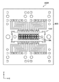
図1Aは、実施形態に係る発光装置を備えた発光モジュールの一例を模式的に示す斜視図である。図1Bは、実施形態に係る発光装置を備えた発光モジュールの一例を模式的に示す平面図である。図1Cは、図1BのIC−IC線における模式断面図である。図1Dは、図1BのID−ID線における模式断面図である。図1Eは、実施形態に係る発光装置の一例を模式的に示す断面図である。図1Fは、実施形態に係る発光装置の一例を模式的に示す下面図である。図1Gは、実施形態に係る発光装置の支持部材の一例を模式的に示す模式平面図である。
<< Embodiment >>
FIG. 1A is a perspective view schematically showing an example of a light emitting module including the light emitting device according to the embodiment. FIG. 1B is a plan view schematically showing an example of a light emitting module including the light emitting device according to the embodiment. FIG. 1C is a schematic cross-sectional view taken along the IC-IC line of FIG. 1B. FIG. 1D is a schematic cross-sectional view taken along the ID-ID line of FIG. 1B. FIG. 1E is a cross-sectional view schematically showing an example of a light emitting device according to an embodiment. FIG. 1F is a bottom view schematically showing an example of a light emitting device according to an embodiment. FIG. 1G is a schematic plan view schematically showing an example of a support member of the light emitting device according to the embodiment.

発光モジュール200は、発光装置100と、発光装置100が載置されたモジュール基板80と、を備えている。 The light emitting module 200 includes a light emitting device 100 and a module substrate 80 on which the light emitting device 100 is mounted.

[発光装置]
はじめに、発光装置100について説明する。
発光装置100は、上面に複数の発光面を備える。
発光装置100は、基板10と、基板10上に載置された発光素子20と、発光素子20上に配置された透光性部材30と、を備える素子構造体15であって、少なくとも3個が一方向Xに沿って配置される複数の素子構造体15と、それぞれの素子構造体15の基板10と発光素子20と透光性部材30の側面を被覆する第1被覆部材51と、第1被覆部材51の側面を被覆し、一方向Xにおいて複数の素子構造体15の側方に亘って配置され、第1被覆部材51よりも剛性が高い支持部材60と、を備えている。
[Light emitting device]
First, the light emitting device 100 will be described.
The light emitting device 100 includes a plurality of light emitting surfaces on the upper surface.
The light emitting device 100 is an element structure 15 including a substrate 10, a light emitting element 20 mounted on the substrate 10, and a translucent member 30 arranged on the light emitting element 20, and is at least three. A plurality of element structures 15 in which the elements are arranged along one direction X, a first covering member 51 that covers the side surfaces of the substrate 10, the light emitting element 20, and the translucent member 30 of each element structure 15, and a first It is provided with a support member 60 that covers the side surface of one covering member 51, is arranged over the sides of a plurality of element structures 15 in one direction X, and has higher rigidity than the first covering member 51.

発光装置100は、主として、素子構造体15と、第1被覆部材51と、支持部材60と、を備えている。
素子構造体15は、主として、基板10と、発光素子20と、保護素子25と、透光性部材30と、導光部材40と、第3被覆部材53と、第2被覆部材52と、を備えている。素子構造体15の外観形状は、例えば、略直方体である。素子構造体15の上面は透光性部材30の上面と、透光性部材30の上面を取り囲む第2被覆部材52の上面とを含む。素子構造体15の側面は第2被覆部材52の側面と基板10の側面とを含む。素子構造体15の下面は、基板10の下面を含む。また、素子構造体15は、透光性部材30の上面に垂直な方向からの平面視で、発光素子20及び透光性部材30は基板10に内包されている。更に、発光素子20及び透光性部材30はどちらか一方がもう一方に内包されていることが好ましい。
発光装置100は、複数の素子構造体15それぞれが発光素子20を備えるため、複数の素子構造体15毎に発光素子20を個別に駆動させることができる。
以下、発光装置100の各構成について説明する。
The light emitting device 100 mainly includes an element structure 15, a first covering member 51, and a support member 60.
The element structure 15 mainly includes a substrate 10, a light emitting element 20, a protective element 25, a translucent member 30, a light guide member 40, a third covering member 53, and a second covering member 52. I have. The external shape of the element structure 15 is, for example, a substantially rectangular parallelepiped. The upper surface of the element structure 15 includes an upper surface of the translucent member 30 and an upper surface of a second covering member 52 surrounding the upper surface of the translucent member 30. The side surface of the element structure 15 includes a side surface of the second covering member 52 and a side surface of the substrate 10. The lower surface of the element structure 15 includes the lower surface of the substrate 10. Further, the element structure 15 is viewed in a plan view from a direction perpendicular to the upper surface of the translucent member 30, and the light emitting element 20 and the translucent member 30 are included in the substrate 10. Further, it is preferable that one of the light emitting element 20 and the translucent member 30 is included in the other.
In the light emitting device 100, since each of the plurality of element structures 15 includes a light emitting element 20, the light emitting element 20 can be individually driven for each of the plurality of element structures 15.
Hereinafter, each configuration of the light emitting device 100 will be described.

基板10は、発光素子20及び保護素子25を載置する部材である。基板10は、例えば平面視略矩形の板状である。これにより、発光装置100において、複数の素子構造体15を近接させて配置することができる。
基板10は、基体1と、基体1の上面、下面、及び内部に、発光素子20や外部電源と電気的に接続するための配線を備えている。配線の材料としては、例えば、Fe、Cu、Ni、Al、Ag、Au、Pt、Ti、W、Pd等の金属又は、これらの少なくとも一種を含む合金等が挙げられる。
基板10としては、例えば発光素子20が載置される上面に発光素子20と接続される上面配線2を備え、発光素子20が載置される上面と反対側の下面に外部電源と電気的に接続される外部接続電極3(例えば、アノード電極3a及びカソード電極3b)を備えるものが挙げられる。この場合、上面配線2と外部接続電極3とは、上面及び下面の双方におよぶ、つまり基体1を貫通するビア4を備えていてもよい。これによって、上面配線2と外部接続電極3とが電気的に接続される。基体1は単層からなるものであってもよいし、複数の層からなるものであってもよい。基体1が複数の層からなる場合、各層を貫通するビアが各層間に配置される内層配線を介して、上面配線2と下面の外部接続電極3とを電気的に接続してもよい。
The substrate 10 is a member on which the light emitting element 20 and the protective element 25 are placed. The substrate 10 has, for example, a plate shape having a substantially rectangular shape in a plan view. As a result, in the light emitting device 100, a plurality of element structures 15 can be arranged in close proximity to each other.
The substrate 10 includes a substrate 1 and wiring on the upper surface, the lower surface, and the inside of the substrate 1 for electrically connecting to the light emitting element 20 and an external power source. Examples of the wiring material include metals such as Fe, Cu, Ni, Al, Ag, Au, Pt, Ti, W, and Pd, or alloys containing at least one of these.
The substrate 10 is provided with, for example, an upper surface wiring 2 connected to the light emitting element 20 on the upper surface on which the light emitting element 20 is mounted, and is electrically connected to an external power source on the lower surface opposite to the upper surface on which the light emitting element 20 is mounted. Examples include those provided with an external connection electrode 3 (for example, an anode electrode 3a and a cathode electrode 3b) to be connected. In this case, the upper surface wiring 2 and the external connection electrode 3 may include vias 4 extending over both the upper surface and the lower surface, that is, penetrating the substrate 1. As a result, the top surface wiring 2 and the external connection electrode 3 are electrically connected. The substrate 1 may be composed of a single layer or may be composed of a plurality of layers. When the substrate 1 is composed of a plurality of layers, the upper surface wiring 2 and the lower surface external connection electrode 3 may be electrically connected via the inner layer wiring in which vias penetrating each layer are arranged between the layers.

基体1としては、絶縁性材料を用いることが好ましく、かつ、発光素子20から出射される光や外光等を透過しにくい材料を用いることが好ましい。例えば、アルミナ、窒化アルミニウム、ムライト等のセラミックス、PA(ポリアミド)、PPA(ポリフタルアミド)、PPS(ポリフェニレンサルファイド)、又は、液晶ポリマー等の熱可塑性樹脂や、エポキシ樹脂、シリコーン樹脂、変性エポキシ樹脂、ウレタン樹脂、又は、フェノール樹脂等の樹脂を用いることができる。なかでも放熱性に優れるセラミックスを用いることが好ましい。 As the substrate 1, it is preferable to use an insulating material, and it is preferable to use a material that does not easily transmit light emitted from the light emitting element 20, external light, or the like. For example, ceramics such as alumina, aluminum nitride and mulite, thermoplastic resins such as PA (polyamide), PPA (polyphthalamide), PPS (polyphenylene sulfide) or liquid crystal polymers, epoxy resins, silicone resins and modified epoxy resins. , Urethane resin, or resin such as phenol resin can be used. Of these, it is preferable to use ceramics having excellent heat dissipation.

発光装置100において、隣接する素子構造体15間の距離L1は0.01mm以上0.15mm以下とすることが好ましい。これにより、素子構造体15間に配置される第1被覆部材51の厚みを0.01mm以上0.15mm以下として、隣接する素子構造体15同士を近接させて接合させることができる。また、複数の素子構造体15を備える発光装置100において、複数の素子構造体15それぞれが基板10を備え、かつ、基板10間に第1被覆部材51が配置されることにより、個々の素子構造体15で発生した熱及び発光装置実装時の熱履歴等に起因する基板10の膨張又は縮小による熱応力の影響を抑制することができる。 In the light emitting device 100, the distance L1 between the adjacent element structures 15 is preferably 0.01 mm or more and 0.15 mm or less. As a result, the thickness of the first covering member 51 arranged between the element structures 15 is set to 0.01 mm or more and 0.15 mm or less, and the adjacent element structures 15 can be brought close to each other and joined to each other. Further, in the light emitting device 100 including the plurality of element structures 15, each of the plurality of element structures 15 is provided with the substrate 10, and the first covering member 51 is arranged between the substrates 10, whereby the individual element structures are formed. It is possible to suppress the influence of thermal stress due to expansion or contraction of the substrate 10 due to the heat generated in the body 15 and the heat history at the time of mounting the light emitting device.

発光素子20は、基板10上に載置されている。発光素子20の形状や大きさ等は任意のものを選択できる。発光素子20の平面視形状は、例えば矩形状である。また例えば、高出力な発光装置を実現するために、発光素子20の平面視における縦及び横の寸法は600μm以上であることが好ましく、800μm以上であることがより好ましい。また、発光強度の均一性、実装のし易さ等の観点から、縦及び横の寸法は1500μm以下であることが好ましい。
発光素子20の発光色としては、用途に応じて任意の波長のものを選択することができる。例えば、青色系(波長430〜500nmの光)、緑色系(波長500〜570nmの光)の発光素子20としては、窒化物系半導体(InAlGa1−X−YN、0≦X、0≦Y、X+Y≦1)、GaP等を用いたものを使用することができる。赤色系(波長610〜700nmの光)の発光素子20としては、窒化物系半導体素子の他にもGaAlAs、AlInGaP等を用いることができる。
The light emitting element 20 is mounted on the substrate 10. Any shape, size, etc. of the light emitting element 20 can be selected. The plan view shape of the light emitting element 20 is, for example, a rectangular shape. Further, for example, in order to realize a high-power light emitting device, the vertical and horizontal dimensions of the light emitting element 20 in a plan view are preferably 600 μm or more, and more preferably 800 μm or more. Further, from the viewpoint of uniformity of light emission intensity, ease of mounting, etc., the vertical and horizontal dimensions are preferably 1500 μm or less.
As the emission color of the light emitting element 20, one having an arbitrary wavelength can be selected depending on the intended use. For example, as the light emitting element 20 of a blue system (light having a wavelength of 430 to 500 nm) and a green system (light having a wavelength of 500 to 570 nm), a nitride semiconductor (In X Al Y Ga 1-XY N, 0 ≦ X) , 0 ≦ Y, X + Y ≦ 1), GaP and the like can be used. As the red light emitting device 20 (light having a wavelength of 610 to 700 nm), GaAlAs, AlInGaP, or the like can be used in addition to the nitride semiconductor device.

発光素子20は、一つの面に正負の素子電極を備えるものを用いることが好ましく、これにより、導電性接着材8により基板10上で配線にフリップチップ実装することができる。導電性接着材8としては、例えば共晶はんだ、導電ペースト、バンプ等を用いればよい。 As the light emitting element 20, it is preferable to use one having positive and negative element electrodes on one surface, whereby the conductive adhesive material 8 can be flip-chip mounted on the wiring on the substrate 10. As the conductive adhesive material 8, for example, eutectic solder, conductive paste, bumps, or the like may be used.

保護素子25は、例えば、ツェナーダイオードを用いることができる。保護素子25は、一つの面に正負の素子電極を備え、導電性接着材8により基板10上で配線にフリップチップ実装されている。なお、発光装置は、保護素子25を備えないものであってもよい。保護素子25の平面視形状は、例えば矩形状である。 As the protection element 25, for example, a Zener diode can be used. The protective element 25 is provided with positive and negative element electrodes on one surface, and is flip-chip mounted on the wiring on the substrate 10 by the conductive adhesive material 8. The light emitting device may not include the protective element 25. The plan view shape of the protective element 25 is, for example, a rectangular shape.

透光性部材30は、発光素子20上に配置され、発光素子20から出射される光を透過して外部に放出する部材である。透光性部材30は、発光素子20からの光及び/又は発光素子20からの光が波長変換された光(例えば、波長320nm〜850nmの範囲の光)の60%以上を透過するものが挙げられ、70%以上の光を透過するものが好ましい。
透光性部材30は、個々の素子構造体15及び発光装置100の主たる発光面となる上面と、上面と対向する下面とを有する板状の部材である。透光性部材30は、例えば、ガラス、セラミックス、サファイア等の無機材料、シリコーン樹脂、変性シリコーン樹脂、エポキシ樹脂、変性エポキシ樹脂、アクリル樹脂、フェノール樹脂、フッ素樹脂のうちの一種以上を含む樹脂又はハイブリッド樹脂等の有機材料のいずれによって形成されていてもよい。透光性部材30は、発光素子20上に配置されている。透光性部材30は、発光素子20の上面よりも広い上面及び/又は下面を有していることが好ましく、平面視で発光素子20を内包するように配置されていることが好ましい。
The translucent member 30 is a member that is arranged on the light emitting element 20 and transmits the light emitted from the light emitting element 20 and emits it to the outside. Examples of the translucent member 30 include those that transmit 60% or more of the light from the light emitting element 20 and / or the light from the light emitting element 20 with wavelength-converted light (for example, light in the wavelength range of 320 nm to 850 nm). It is preferable that the light is transmitted by 70% or more.
The translucent member 30 is a plate-shaped member having an upper surface serving as a main light emitting surface of each element structure 15 and a light emitting device 100, and a lower surface facing the upper surface. The translucent member 30 is, for example, a resin containing one or more of inorganic materials such as glass, ceramics, and sapphire, silicone resin, modified silicone resin, epoxy resin, modified epoxy resin, acrylic resin, phenol resin, and fluororesin. It may be formed of any organic material such as a hybrid resin. The translucent member 30 is arranged on the light emitting element 20. The translucent member 30 preferably has an upper surface and / or a lower surface wider than the upper surface of the light emitting element 20, and is preferably arranged so as to include the light emitting element 20 in a plan view.

発光装置100の上面において、隣接する透光性部材30間の距離L2は0.2mm以下とすることが好ましい。これにより、例えば、発光装置100を車の配光可変型ヘッドライトの光源に用いる場合、光源を小さくすることができ、ヘッドライトレンズのサイズを小さくすることができる。
つまり、発光装置100の上面において、隣接する透光性部材30間(つまり隣接する発光面間)は非発光領域であるため、隣接する透光性部材30を同時に点灯させた際に、被照射領域に暗部が生じる虞がある。このため、被照射領域において暗部が生じないように、例えば、プライマリーレンズを用いて複数の発光面の焦点位置を調節する等、光学系の構成を最適化する必要がある。これに対して、本実施形態に係る発光装置100では、隣接する発光面(つまり透光性部材30の上面)間の距離L2を0.2mm以下と小さくすることができる。このため、光学系においてプライマリーレンズを省略する等、レンズ等の光学系を含む灯具全体の構成の簡略化や小型化を図ることができる。また、レンズを省略することで、光学系を通過する際の光のロスを少なくすることができる。
隣接する透光性部材30間の距離L2は、より好ましくは0.1mm以下である。透光性部材30間の距離L2は、素子構造体15及び発光装置100の製造のし易さの観点から、例えば、0.02mm以上が挙げられる。
On the upper surface of the light emitting device 100, the distance L2 between the adjacent translucent members 30 is preferably 0.2 mm or less. Thereby, for example, when the light emitting device 100 is used as a light source of a variable light distribution type headlight of a car, the light source can be reduced and the size of the headlight lens can be reduced.
That is, on the upper surface of the light emitting device 100, since the space between the adjacent translucent members 30 (that is, the space between the adjacent light emitting surfaces) is a non-light emitting region, when the adjacent translucent members 30 are turned on at the same time, the light is irradiated. There is a risk of dark areas appearing in the area. Therefore, it is necessary to optimize the configuration of the optical system, for example, by adjusting the focal positions of a plurality of light emitting surfaces by using a primary lens so that a dark portion does not occur in the irradiated region. On the other hand, in the light emitting device 100 according to the present embodiment, the distance L2 between adjacent light emitting surfaces (that is, the upper surface of the translucent member 30) can be reduced to 0.2 mm or less. Therefore, the configuration of the entire lamp including the optical system such as the lens can be simplified or downsized by omitting the primary lens in the optical system. Further, by omitting the lens, it is possible to reduce the loss of light when passing through the optical system.
The distance L2 between the adjacent translucent members 30 is more preferably 0.1 mm or less. The distance L2 between the translucent members 30 is, for example, 0.02 mm or more from the viewpoint of ease of manufacturing the element structure 15 and the light emitting device 100.

透光性部材30の平面形状は、例えば、矩形状である。これにより、複数の発光面を高密度に近接させて配置することができる。なかでも、発光素子20の平面形状と類似する形状であることがより好ましい。透光性部材30の下面の面積は、発光素子20の上面の面積の0.8〜1.5倍程度であることが好ましい。透光性部材30の厚みは、全体にわたって一定であってもよいし、一部が薄く又は厚くてもよい。透光性部材30の厚みは、例えば、50μm以上300μm以下の範囲とすることができる。 The planar shape of the translucent member 30 is, for example, a rectangular shape. As a result, a plurality of light emitting surfaces can be arranged in close proximity to each other at high density. Above all, it is more preferable that the shape is similar to the planar shape of the light emitting element 20. The area of the lower surface of the translucent member 30 is preferably about 0.8 to 1.5 times the area of the upper surface of the light emitting element 20. The thickness of the translucent member 30 may be constant throughout, or may be partially thin or thick. The thickness of the translucent member 30 can be, for example, in the range of 50 μm or more and 300 μm or less.

透光性部材30は、入射された光の少なくとも一部を波長変換可能な蛍光体を含有してもよい。蛍光体を含有する透光性部材30は、例えば、蛍光体の焼結体や、上述した材料に蛍光体を含有させたものが挙げられる。また、透光性部材30は、樹脂、ガラス、セラミック等の成形体の表面に蛍光体を含有する樹脂層や蛍光体を含有するガラス層等の蛍光体層を備えるものでもよい。また、透光性部材30は、目的に応じて、拡散材等のフィラーを含有してもよい。また、拡散材等のフィラーを含有する場合、透光性部材30は、上述した材料にフィラーを含有させたものでもよいし、樹脂、ガラス、セラミック等の成形体の表面にフィラーを含有する樹脂層やフィラーを含有するガラス層等の拡散材層を備えたものでもよい。 The translucent member 30 may contain a phosphor capable of wavelength-converting at least a part of the incident light. Examples of the translucent member 30 containing a fluorescent substance include a sintered body of the fluorescent substance and a material in which the fluorescent substance is contained in the above-mentioned material. Further, the translucent member 30 may be provided with a phosphor layer such as a resin layer containing a phosphor or a glass layer containing a phosphor on the surface of a molded body such as resin, glass or ceramic. Further, the translucent member 30 may contain a filler such as a diffusing material, depending on the purpose. When a filler such as a diffusing material is contained, the translucent member 30 may be a material containing a filler in the above-mentioned material, or a resin containing a filler on the surface of a molded product such as resin, glass, or ceramic. It may be provided with a diffuser layer such as a layer or a glass layer containing a filler.

蛍光体としては、当該分野で公知のものを使用することができる。例えば、緑色発光する蛍光体としては、イットリウム・アルミニウム・ガーネット系蛍光体(例えばY(Al,Ga)12:Ce)、ルテチウム・アルミニウム・ガーネット系蛍光体(例えばLu(Al,Ga)12:Ce)、テルビウム・アルミニウム・ガーネット系蛍光体(例えばTb(Al,Ga)12:Ce)系蛍光体、シリケート系蛍光体(例えば(Ba,Sr)SiO:Eu)、クロロシリケート系蛍光体(例えばCaMg(SiOl2:Eu)、βサイアロン系蛍光体(例えばSi6−zAl8−z:Eu(0<z<4.2))、SGS系蛍光体(例えばSrGa:Eu)等が挙げられる。黄色発光する蛍光体としては、αサイアロン系蛍光体(例えばMz(Si,Al)12(O,N)16(但し、0<z≦2であり、MはLi、Mg、Ca、Y、及びLaとCeを除くランタニド元素)等が挙げられる。この他、上記緑色発光する蛍光体の中には黄色発光する蛍光体もある。 As the phosphor, those known in the art can be used. For example, a phosphor emitting green light, yttrium-aluminum-garnet fluorescent material (e.g., Y 3 (Al, Ga) 5 O 12: Ce), lutetium-aluminum-garnet fluorescent material (e.g., Lu 3 (Al, Ga ) 5 O 12 : Ce), terbium-aluminum-garnet-based phosphor (for example, Tb 3 (Al, Ga) 5 O 12 : Ce) -based phosphor, silicate-based phosphor (for example, (Ba, Sr) 2 SiO 4 : Eu), chlorosilicate-based phosphors (for example, Ca 8 Mg (SiO 4 ) 4 C l2 : Eu), β-sialon-based phosphors (for example, Si 6-z Al z Oz N 8-z : Eu (0 <z < 4.2)), SGS-based phosphors (for example, SrGa 2 S 4 : Eu) and the like can be mentioned. Examples of the fluorescent substance that emits yellow light include α-sialon-based phosphors (for example, Mz (Si, Al) 12 (O, N) 16 (where 0 <z ≦ 2 and M is Li, Mg, Ca, Y, and (Lanthanide element excluding La and Ce) and the like. In addition, among the above-mentioned phosphors that emit green light, there are also phosphors that emit yellow light.

また例えば、イットリウム・アルミニウム・ガーネット系蛍光体は、Yの一部をGdで置換することにより、発光ピーク波長を長波長側にシフトさせることができ、黄色発光が可能である。また、これらの中には、橙色発光が可能な蛍光物質もある。赤色発光する蛍光体としては、窒素含有アルミノ珪酸カルシウム(CASN又はSCASN)系蛍光体(例えば(Sr,Ca)AlSiN:Eu)、BSESN系蛍光体(例えば(Ba,Sr,Ca)Si:Eu)等が挙げられる。この他、マンガン賦活フッ化物系蛍光体(一般式(I)A[M1−aMn]で表される蛍光体である(但し、上記一般式(I)中、Aは、K、Li、Na、Rb、Cs及びNHからなる群から選ばれる少なくとも一種であり、Mは、第4族元素及び第14族元素からなる群から選ばれる少なくとも一種の元素であり、aは0<a<0.2を満たす))が挙げられる。このマンガン賦活フッ化物系蛍光体の代表例としては、マンガン賦活フッ化珪酸カリウムの蛍光体(例えばKSiF:Mn)がある。 Further, for example, in the yttrium aluminum garnet-based phosphor, the emission peak wavelength can be shifted to the long wavelength side by substituting a part of Y with Gd, and yellow emission is possible. In addition, some of these fluorescent substances can emit orange light. Examples of the phosphor that emits red light include a nitrogen-containing calcium aluminosilicate (CASN or SCASN) -based phosphor (for example, (Sr, Ca) AlSiN 3 : Eu) and a BSESN-based phosphor (for example, (Ba, Sr, Ca) 2 Si 5). N 8 : Eu) and the like. In addition, it is a manganese-activated fluoride-based phosphor (general formula (I) A 2 [M 1-a Mn a F 6 ]) (however, in the above general formula (I), A is a phosphor. At least one element selected from the group consisting of K, Li, Na, Rb, Cs and NH 4 , M is at least one element selected from the group consisting of Group 4 elements and Group 14 elements, and a is 0 <a <0.2 is satisfied)). Typical examples of the manganese-activated fluoride phosphors, phosphor manganese-activated fluoride potassium silicate (e.g. K 2 SiF 6: Mn) is.

拡散材としては、当該分野で公知のものを使用することができる。例えば、シリカ、アルミナ、チタン酸バリウム、酸化チタン等を用いることができる。
また蛍光体層や拡散材層のバインダーとして樹脂を用いる場合、樹脂としては、例えば、エポキシ樹脂、変性エポキシ樹脂、シリコーン樹脂、変性シリコーン樹脂等の熱硬化性樹脂等が挙げられる。
As the diffusing material, a material known in the art can be used. For example, silica, alumina, barium titanate, titanium oxide and the like can be used.
When a resin is used as a binder for the phosphor layer and the diffusing material layer, examples of the resin include thermosetting resins such as epoxy resin, modified epoxy resin, silicone resin, and modified silicone resin.

導光部材40は、透光性部材30と発光素子20の間及び/又は発光素子20の側面に配置される。導光部材40は、発光素子20から光を取り出し易くし、発光素子20からの光を透光性部材30に導光する部材である。導光部材40は、例えば、発光素子20と透光性部材30とを接合する接着部材である。発光素子20と透光性部材30とを接合する導光部材40は、透光性部材30と発光素子20の間から延在し、発光素子20の側面にも配置されていることが好ましい。これにより、発光素子20の側面から出射される光を透光性部材30へと導光させて、発光素子20からの光の取り出し効率を向上させることができる。 The light guide member 40 is arranged between the translucent member 30 and the light emitting element 20 and / or on the side surface of the light emitting element 20. The light guide member 40 is a member that facilitates the extraction of light from the light emitting element 20 and guides the light from the light emitting element 20 to the translucent member 30. The light guide member 40 is, for example, an adhesive member that joins the light emitting element 20 and the translucent member 30. It is preferable that the light guide member 40 that joins the light emitting element 20 and the translucent member 30 extends from between the translucent member 30 and the light emitting element 20 and is also arranged on the side surface of the light emitting element 20. As a result, the light emitted from the side surface of the light emitting element 20 can be guided to the translucent member 30, and the efficiency of extracting the light from the light emitting element 20 can be improved.

導光部材40は、断面視で、発光素子20の下面側(つまり、基板10との接合面側)から透光性部材30に向かって、幅が広がるように傾斜した形状を有する。このような形態とすることで、発光素子20から横方向に進む光が上方に反射され易くなるため、光の取り出し効率がより向上する。ただし、導光部材40の外側面の断面形状は、直線形状であってもよく、湾曲形状であってもよい。例えば、断面視における導光部材40の外側面が湾曲形状である場合、湾曲形状は、第3被覆部材53側に凹む湾曲形状でもよいし、発光素子20側に凹む湾曲形状でもよい。 The light guide member 40 has a shape that is inclined so as to widen from the lower surface side of the light emitting element 20 (that is, the joint surface side with the substrate 10) toward the translucent member 30 in a cross-sectional view. With such a form, the light traveling in the lateral direction from the light emitting element 20 is easily reflected upward, so that the light extraction efficiency is further improved. However, the cross-sectional shape of the outer surface of the light guide member 40 may be a straight line shape or a curved shape. For example, when the outer surface of the light guide member 40 in the cross-sectional view is a curved shape, the curved shape may be a curved shape recessed toward the third covering member 53 side or a curved shape recessed toward the light emitting element 20 side.

導光部材40は、発光素子20の側面のうち発光部を含む領域を被覆すればよいが、光の取り出し効率を向上させる観点から、発光素子20の側面の略全部を被覆していることがより好ましい。
導光部材40としては、例えば、透光性の樹脂を用いることができる。また、導光部材40は、例えば、前記した透光性部材30に用いる樹脂等が挙げられる。また、前記した拡散材が含有されていてもよい。これにより、透光性部材30に、より均等に光を入射することができ、発光装置100の色ムラを抑制することができる。
The light guide member 40 may cover a region of the side surface of the light emitting element 20 including the light emitting portion, but from the viewpoint of improving the light extraction efficiency, it may cover almost all the side surfaces of the light emitting element 20. More preferred.
As the light guide member 40, for example, a translucent resin can be used. Further, the light guide member 40 includes, for example, the resin used for the translucent member 30 described above. Further, the above-mentioned diffusing material may be contained. As a result, the light can be more evenly incident on the translucent member 30, and the color unevenness of the light emitting device 100 can be suppressed.

第3被覆部材53は、基板10上において発光素子20の周囲に設けられる。第3被覆部材53は発光素子20の側面を被覆し、発光素子20の側面から基板10の上面まで延在して設けられている。第3被覆部材53は、基板10と発光素子20との接着力を高めることができる。第3被覆部材53は、ここでは導光部材40を介して発光素子20の側面を被覆している。
第3被覆部材53は、透光性部材30側から基板10側に向かって、発光素子20の側面に沿ってフィレット状に形成されている。言い換えると、第3被覆部材53の外側面の断面形状は、例えば透光性部材30側から基板10に向かって部材幅が広がるように傾斜した形状を有する。第3被覆部材53の外側面の断面形状は、直線形状であってもよく、湾曲形状であってもよい。例えば、断面視における第3被覆部材53の外側面が湾曲形状である場合、第3被覆部材53の湾曲形状は、第2被覆部材52側に凹む湾曲形状でもよいし、発光素子20側に凹む湾曲形状でもよい。
The third covering member 53 is provided around the light emitting element 20 on the substrate 10. The third covering member 53 covers the side surface of the light emitting element 20, and is provided so as to extend from the side surface of the light emitting element 20 to the upper surface of the substrate 10. The third covering member 53 can increase the adhesive force between the substrate 10 and the light emitting element 20. Here, the third covering member 53 covers the side surface of the light emitting element 20 via the light guide member 40.
The third covering member 53 is formed in a fillet shape along the side surface of the light emitting element 20 from the translucent member 30 side toward the substrate 10 side. In other words, the cross-sectional shape of the outer surface of the third covering member 53 has, for example, a shape inclined so that the width of the member widens from the translucent member 30 side toward the substrate 10. The cross-sectional shape of the outer surface of the third covering member 53 may be a straight line shape or a curved shape. For example, when the outer surface of the third covering member 53 in cross-sectional view has a curved shape, the curved shape of the third covering member 53 may be a curved shape recessed toward the second covering member 52 or recessed toward the light emitting element 20 side. It may have a curved shape.

第3被覆部材53は、樹脂を用いることが好ましい。第3被覆部材53は、例えば、光反射性を有する白色樹脂により形成することができる。
第3被覆部材53としては、例えば、透光性の樹脂に反射材を含有させたものを用いることができる。第3被覆部材53に用いる樹脂としては、例えば、エポキシ樹脂、変性エポキシ樹脂、シリコーン樹脂、変性シリコーン樹脂等が挙げられる。特に、耐光性、耐熱性に優れるシリコーン樹脂を用いることが好ましい。反射材としては、例えば、酸化チタン、シリカ、アルミナ、酸化ジルコニウム、酸化マグネシウム、チタン酸カリウム、酸化亜鉛、窒化ケイ素、窒化硼素等が挙げられる。なかでも、光反射の観点から、屈折率が比較的高い酸化チタンを用いることが好ましい。
It is preferable to use a resin for the third covering member 53. The third covering member 53 can be formed of, for example, a white resin having light reflectivity.
As the third covering member 53, for example, a translucent resin containing a reflective material can be used. Examples of the resin used for the third coating member 53 include an epoxy resin, a modified epoxy resin, a silicone resin, and a modified silicone resin. In particular, it is preferable to use a silicone resin having excellent light resistance and heat resistance. Examples of the reflective material include titanium oxide, silica, alumina, zirconium oxide, magnesium oxide, potassium titanate, zinc oxide, silicon nitride, boron nitride and the like. Among them, it is preferable to use titanium oxide having a relatively high refractive index from the viewpoint of light reflection.

第3被覆部材53は、発光素子20の側面の少なくとも一部を被覆すればよい。好ましくは、第3被覆部材53が発光素子20の側面全体を被覆するのがよい。更に好ましくは、発光素子20の側面から延在して透光性部材30の側面の少なくとも一部を被覆することがよい。これにより、個々の素子構造体15において、発光素子20の側面から出射された光の横方向への漏れを抑制することができる。そして、複数の素子構造体15を備える発光装置100において、隣接する素子構造体15への光漏れが抑制され、発光むらの少ない発光装置100とすることができる。また、第3被覆部材53が透光性部材30の側面を被覆することで、素子構造体15の光学特性を測定する際に、素子構造体15の色度座標を把握し易くなる等、より容易に測定することができる。また、後述するように、素子構造体15毎に個片化された後に選別工程を行う際に、素子構造体15の色度座標をより把握し易くなる。 The third covering member 53 may cover at least a part of the side surface of the light emitting element 20. Preferably, the third covering member 53 covers the entire side surface of the light emitting element 20. More preferably, it extends from the side surface of the light emitting element 20 and covers at least a part of the side surface of the translucent member 30. As a result, in each element structure 15, it is possible to suppress lateral leakage of light emitted from the side surface of the light emitting element 20. Then, in the light emitting device 100 including the plurality of element structures 15, light leakage to the adjacent element structures 15 is suppressed, and the light emitting device 100 with less uneven light emission can be obtained. Further, since the third covering member 53 covers the side surface of the translucent member 30, it becomes easier to grasp the chromaticity coordinates of the element structure 15 when measuring the optical characteristics of the element structure 15. It can be easily measured. Further, as will be described later, when the sorting step is performed after each element structure 15 is separated into individual pieces, the chromaticity coordinates of the element structure 15 can be more easily grasped.

第3被覆部材53は、発光素子20と基板10との間にも配置されることが好ましい。これにより、発光素子20から下方に進む光が第3被覆部材53で反射され、発光装置100の光取り出し効率をより向上させることができる。 It is preferable that the third covering member 53 is also arranged between the light emitting element 20 and the substrate 10. As a result, the light traveling downward from the light emitting element 20 is reflected by the third coating member 53, and the light extraction efficiency of the light emitting device 100 can be further improved.

発光装置100は、複数の素子構造体15を備え、複数の素子構造体15それぞれが発光素子20の側面を被覆する第3被覆部材53を備えるため、発光素子20から出射された光の横方向への光漏れを抑制することができる。これにより、個々の素子構造体15の光取り出し効率を低下させることなく、複数の素子構造体15をより近接して配置させることが可能となる。 Since the light emitting device 100 includes a plurality of element structures 15 and each of the plurality of element structures 15 includes a third covering member 53 that covers the side surface of the light emitting element 20, the light emitted from the light emitting element 20 in the lateral direction. It is possible to suppress light leakage to. This makes it possible to arrange the plurality of element structures 15 closer to each other without lowering the light extraction efficiency of the individual element structures 15.

第2被覆部材52は、基板10上で発光素子20の側面及び透光性部材30の側面を被覆する部材である。第2被覆部材52は、導光部材40及び第3被覆部材53を介して発光素子20の側面を被覆すると共に透光性部材30の側面を被覆している。
第2被覆部材52を備えることにより、素子構造体15は、外観形状を略直方体とすることができる。これにより、発光装置100は、素子構造体15間において、第1被覆部材51を素子構造体15の下面から上面まで略同じ幅で配置することができる。
The second covering member 52 is a member that covers the side surface of the light emitting element 20 and the side surface of the translucent member 30 on the substrate 10. The second covering member 52 covers the side surface of the light emitting element 20 and the side surface of the translucent member 30 via the light guide member 40 and the third covering member 53.
By providing the second covering member 52, the element structure 15 can have a substantially rectangular parallelepiped appearance. As a result, the light emitting device 100 can arrange the first covering member 51 between the element structures 15 with substantially the same width from the lower surface to the upper surface of the element structure 15.

第2被覆部材52は樹脂を用いることが好ましい。第2被覆部材52は、例えば、光反射性を有する白色樹脂により形成することができる。第2被覆部材52は、発光素子20の側面及び透光性部材30の側面を被覆する。第2被覆部材52に用いる樹脂としては、例えば、第3被覆部材53に用いる樹脂として例示したものが挙げられる。第2被覆部材52に用いる樹脂に含有する反射材としては、例えば、第3被覆部材53に用いる反射材として例示したものが挙げられる。 It is preferable to use a resin for the second covering member 52. The second covering member 52 can be formed of, for example, a white resin having light reflectivity. The second covering member 52 covers the side surface of the light emitting element 20 and the side surface of the translucent member 30. Examples of the resin used for the second covering member 52 include those exemplified as the resin used for the third covering member 53. Examples of the reflective material contained in the resin used for the second coating member 52 include those exemplified as the reflective material used for the third coating member 53.

第1被覆部材51は、複数の素子構造体15の周囲に設けられた部材である。第1被覆部材51は樹脂を用いることが好ましい。第1被覆部材51は、例えば、透光性の樹脂に反射材を含有させた白色樹脂により形成することができる。第1被覆部材51は、素子構造体15の側面を被覆する。すなわち、第1被覆部材51は、基板10の側面を被覆し、導光部材40、第3被覆部材53及び第2被覆部材52を介して発光素子20の側面を被覆し、第2被覆部材52を介して透光性部材30の側面を被覆している。第1被覆部材51は、互いに隣接する素子構造体15間にも設けられており、素子構造体15の上面を露出させて、複数の素子構造体15それぞれの側面を被覆している。 The first covering member 51 is a member provided around the plurality of element structures 15. It is preferable to use a resin for the first covering member 51. The first covering member 51 can be formed of, for example, a white resin in which a reflective material is contained in a translucent resin. The first covering member 51 covers the side surface of the element structure 15. That is, the first covering member 51 covers the side surface of the substrate 10 and covers the side surface of the light emitting element 20 via the light guide member 40, the third covering member 53, and the second covering member 52, and the second covering member 52. Covers the side surface of the translucent member 30 via. The first covering member 51 is also provided between the element structures 15 adjacent to each other, and exposes the upper surface of the element structure 15 to cover the side surfaces of each of the plurality of element structures 15.

第1被覆部材51に用いる樹脂としては、例えば、第3被覆部材53に用いる樹脂として例示したものが挙げられる。第1被覆部材51に用いる樹脂に含有する反射材としては、例えば、第3被覆部材53に用いる反射材として例示したものが挙げられる。 Examples of the resin used for the first covering member 51 include those exemplified as the resin used for the third covering member 53. Examples of the reflective material contained in the resin used for the first coating member 51 include those exemplified as the reflective material used for the third coating member 53.

第1被覆部材51は、白色以外の着色された樹脂であってもよい。着色された樹脂とは、例えば、黒色樹脂、灰色樹脂等が挙げられる。黒色樹脂及び灰色樹脂は白色樹脂と比較して光吸収率が高い。このため、素子構造体15間に黒色樹脂又は灰色樹脂である第1被覆部材51が設けられることで、素子構造体15間における横方向への光漏れを効果的に抑制することができる。なお、第1被覆部材51として、黒色樹脂又は灰色樹脂を用いる場合は、黒色樹脂又は灰色樹脂と透光性部材30とが離間して配置されるように、素子構造体15は第2被覆部材52を備える構成とすることが好ましい。これにより、素子構造体15間に黒色樹脂又は灰色樹脂を用いることによる光吸収の影響を抑制することができる。そのため、発光面の光取り出し効率の低下を抑制し、かつ、個別点灯させた際の発光領域と非発光領域とのコントラストが高い、「見切り性」の良好な発光装置とすることができる。黒色樹脂や灰色樹脂としては、例えば、カーボンブラックやグラファイト等の黒色顔料を含有させた樹脂が挙げられる。黒色顔料と上述した反射材等の白色顔料とを組み合わせて、それぞれの添加量を調整することで、黒色や灰色等の色の濃度を調整することができる。また、赤色、青色、緑色等の顔料を組み合わせることで、黒色、灰色、それ以外の所望の色に着色してもよい。
発光装置100は、それぞれが発光面を有する複数の素子構造体15が第1被覆部材51で保持されている。第1被覆部材51により、それぞれの素子構造体15を所望の配置で保持することができるため、複数の発光面を高密度に配置することができる。
The first covering member 51 may be a colored resin other than white. Examples of the colored resin include black resin, gray resin and the like. The black resin and the gray resin have a higher light absorption rate than the white resin. Therefore, by providing the first coating member 51 which is a black resin or a gray resin between the element structures 15, light leakage in the lateral direction between the element structures 15 can be effectively suppressed. When a black resin or a gray resin is used as the first covering member 51, the element structure 15 is a second covering member so that the black resin or the gray resin and the translucent member 30 are arranged apart from each other. It is preferable to have a configuration including 52. Thereby, the influence of light absorption due to the use of the black resin or the gray resin between the element structures 15 can be suppressed. Therefore, it is possible to obtain a light emitting device having a good "parting property", which suppresses a decrease in the light extraction efficiency of the light emitting surface and has a high contrast between the light emitting region and the non-light emitting region when individually lit. Examples of the black resin and gray resin include resins containing a black pigment such as carbon black and graphite. The density of colors such as black and gray can be adjusted by combining the black pigment and the white pigment such as the above-mentioned reflective material and adjusting the addition amount of each. Further, by combining pigments such as red, blue, and green, black, gray, and other desired colors may be colored.
In the light emitting device 100, a plurality of element structures 15 each having a light emitting surface are held by the first covering member 51. Since each element structure 15 can be held in a desired arrangement by the first covering member 51, a plurality of light emitting surfaces can be arranged at a high density.

支持部材60は、第1被覆部材51の側面を被覆し、一方向Xにおいて複数の素子構造体15の側方に亘って配置される部材である。支持部材60は、複数の素子構造体15と対向する辺であって、一方向Xと平行な辺を有する。例えば、支持部材60は、複数の素子構造体15を囲む枠状の部材であってもよい。ここでは、支持部材60は、複数の素子構造体15を取り囲み、第1被覆部材51を支持するための枠体として設けられている。支持部材60は、平面視で例えば略長方形の枠状であり、複数の素子構造体15の周囲に設けられている。 The support member 60 is a member that covers the side surface of the first covering member 51 and is arranged over the sides of the plurality of element structures 15 in one direction X. The support member 60 is a side facing the plurality of element structures 15 and has a side parallel to one direction X. For example, the support member 60 may be a frame-shaped member that surrounds the plurality of element structures 15. Here, the support member 60 is provided as a frame body for surrounding the plurality of element structures 15 and supporting the first covering member 51. The support member 60 has, for example, a substantially rectangular frame shape in a plan view, and is provided around the plurality of element structures 15.

支持部材60は、第1被覆部材51よりも剛性が高い部材、或いは構造で形成されている。具体的には、支持部材60は、第1被覆部材51に反りを生じさせる応力の値(剛性)より高い剛性を有する。ここで、「剛性」とは、曲げや引っ張りの力に対する変形のしづらさを示し、単位変形(曲げ又は引っ張り)を起こすのに必要な力(荷重÷変形量)で表される。部材の剛性の比較は、弾性変形とみなし得る範囲の同じ量の変形を比較する部材に起こすのに必要な力の大小を比較して行う。剛性は、ヤング率(引張弾性率)等の弾性率が大きい材料を使うことによって高くなる。また、剛性は、同じ材料でも板厚を変えられる場合は板厚を厚くすること等により高くなる。複合材料においても、単位変形(曲げ又は引っ張り)を起こすのに必要な力(荷重÷変形量)の大きさで、剛性を比較する。例えば、曲げ試験では、JIS K 7171:2016に則り、曲げ歪み0.05%と0.25%の時の応力を求め、剛性を比較することもできる。 The support member 60 is formed of a member or structure having a higher rigidity than the first covering member 51. Specifically, the support member 60 has a rigidity higher than the value (rigidity) of the stress that causes the first covering member 51 to warp. Here, "rigidity" indicates the difficulty of deformation with respect to bending or pulling force, and is expressed by the force (load ÷ deformation amount) required to cause unit deformation (bending or pulling). The rigidity of the members is compared by comparing the magnitude of the force required to cause the members to be compared with the same amount of deformation within the range that can be regarded as elastic deformation. Rigidity is increased by using a material having a large elastic modulus such as Young's modulus (tensile elastic modulus). Further, if the plate thickness can be changed even with the same material, the rigidity is increased by increasing the plate thickness or the like. Even in composite materials, the rigidity is compared by the magnitude of the force (load ÷ deformation amount) required to cause unit deformation (bending or pulling). For example, in the bending test, the stresses at bending strains of 0.05% and 0.25% can be obtained and the rigidity can be compared according to JIS K 7171: 2016.

発光装置100は、第1被覆部材51よりも剛性が高い支持部材60を有することで、第1被覆部材51の反りの発生が抑制されることにより、発光装置100の反りの発生が抑制される。これにより、発光装置100の実装面が平坦となり、発光装置100をモジュール基板80の所望の位置に精度よく配置することができる。発光装置100は、複数の素子構造体15が第1被覆部材51により連結されている。このため、第1被覆部材51に樹脂を用いる場合、樹脂が硬化時に収縮すること等により、発光装置100に反りが発生する虞がある。しかし、支持部材60に第1被覆部材51よりも剛性が高い材料、例えば、非可撓性の材料を用いることで反りの発生を抑制することができる。これにより、発光装置100のモジュール基板80への実装性が良好となり、複数の発光面が高密度に配置された発光装置100を、モジュール基板80の所望の位置により精度よく配置することができる。 Since the light emitting device 100 has a support member 60 having a higher rigidity than the first covering member 51, the occurrence of warpage of the first covering member 51 is suppressed, so that the generation of warpage of the light emitting device 100 is suppressed. .. As a result, the mounting surface of the light emitting device 100 becomes flat, and the light emitting device 100 can be accurately arranged at a desired position on the module substrate 80. In the light emitting device 100, a plurality of element structures 15 are connected by a first covering member 51. Therefore, when a resin is used for the first covering member 51, the light emitting device 100 may be warped due to shrinkage of the resin during curing or the like. However, by using a material having a higher rigidity than the first covering member 51 for the support member 60, for example, a non-flexible material, the occurrence of warpage can be suppressed. As a result, the mountability of the light emitting device 100 on the module substrate 80 is improved, and the light emitting device 100 in which a plurality of light emitting surfaces are arranged at high density can be accurately arranged at a desired position of the module substrate 80.

支持部材60としては、例えば、金属、合金等の導電性部材、又は、セラミック等の絶縁性部材を用いることができる。導電性部材としては、例えば、Fe、Cu、Ni、Al、Ti、W等の金属や、例えば、Fe、Cu、Ni、Al、Ag、Au、Pt、Ti、W、Pd等のうちの少なくとも一種を含む合金が挙げられる。絶縁性部材としては、例えば、酸化アルミニウム、窒化アルミニウム等のセラミックス、フェノール樹脂、エポキシ樹脂、シリコーン樹脂、ポリイミド樹脂、BTレジン、ポリフタルアミド等の樹脂成型体が挙げられる。樹脂を用いる場合には、必要に応じて、ガラス繊維、酸化ケイ素、酸化チタン、酸化アルミニウム等の無機フィラーを樹脂に混合してもよい。また、例えば樹脂成型体に金属部材が埋設された支持部材等、支持部材は、これらの材料の複合体を用いてもよい。 As the support member 60, for example, a conductive member such as a metal or an alloy, or an insulating member such as a ceramic can be used. Examples of the conductive member include metals such as Fe, Cu, Ni, Al, Ti, and W, and at least one of Fe, Cu, Ni, Al, Ag, Au, Pt, Ti, W, Pd, and the like. Examples include alloys containing one type. Examples of the insulating member include ceramics such as aluminum oxide and aluminum nitride, and resin molded bodies such as phenol resin, epoxy resin, silicone resin, polyimide resin, BT resin, and polyphthalamide. When a resin is used, an inorganic filler such as glass fiber, silicon oxide, titanium oxide, or aluminum oxide may be mixed with the resin, if necessary. Further, a composite of these materials may be used as the support member, for example, a support member in which a metal member is embedded in a resin molded body.

支持部材60は、複数の素子構造体15を囲む枠状の部材であることが好ましい。更に、支持部材60は、複数の素子構造体15を挟む一方向Xに平行な二辺と、複数の素子構造体15を挟む一方向Xと直交する二辺とを含む平面視略長方形状の開口を有する枠状であることがより好ましい。これにより、支持部材60と接する第1被覆部材51の側面の全てを支持部材60により固定することができるため、反りの発生をより効果的に抑制することができる。 The support member 60 is preferably a frame-shaped member that surrounds the plurality of element structures 15. Further, the support member 60 has a substantially rectangular shape in a plan view including two sides parallel to one direction X sandwiching the plurality of element structures 15 and two sides orthogonal to the one direction X sandwiching the plurality of element structures 15. It is more preferable that it has a frame shape with an opening. As a result, all the side surfaces of the first covering member 51 in contact with the support member 60 can be fixed by the support member 60, so that the occurrence of warpage can be suppressed more effectively.

支持部材60の上面から下面までの高さHは、素子構造体15の上面から下面までの高さより低いことが好ましい。これにより、発光装置100において、支持部材60の上面を、素子構造体15の上面よりも低い位置(つまり発光装置100の下面側)に配置することができる。このような構成とすることで、発光装置100の製造時における、透光性部材30の上面への第1被覆部材51の這い上がりが抑制される。
支持部材60の高さHは、0.1mm以上1.0mm以下であることが好ましい。支持部材60の高さHが0.1mm以上であれば、支持部材60自体の剛性が確保され、発光装置100の反りの発生の抑制効果がより高まり、所望の位置により精度よく配置することができる。一方、支持部材60の高さHが1.0mm以下であれば、発光装置100をより軽量化することができ、また、より小型化することができる。
支持部材60は、複数の素子構造体15の側方に亘って配置される部位の幅Wが0.5mm以上2.0mm以下であることが好ましい。ここで、幅Wとは、支持部材60の、一方向Xに平行な辺であって、素子構造体15と対向して配置される辺における、一方向Xと直交する方向における最短長さを意味する。幅Wが0.5mm以上であれば、支持部材60自体の剛性が確保され、発光装置100の反りの発生の抑制効果がより高まり、所望の位置により精度よく配置することができる。一方、幅Wが2.0mm以下であれば、発光装置100をより軽量化することができ、また、より小型化することができる。
The height H from the upper surface to the lower surface of the support member 60 is preferably lower than the height from the upper surface to the lower surface of the element structure 15. As a result, in the light emitting device 100, the upper surface of the support member 60 can be arranged at a position lower than the upper surface of the element structure 15 (that is, the lower surface side of the light emitting device 100). With such a configuration, the crawling of the first covering member 51 onto the upper surface of the translucent member 30 at the time of manufacturing the light emitting device 100 is suppressed.
The height H of the support member 60 is preferably 0.1 mm or more and 1.0 mm or less. When the height H of the support member 60 is 0.1 mm or more, the rigidity of the support member 60 itself is ensured, the effect of suppressing the occurrence of warpage of the light emitting device 100 is further enhanced, and the support member 60 can be arranged accurately at a desired position. can. On the other hand, when the height H of the support member 60 is 1.0 mm or less, the light emitting device 100 can be made lighter and smaller.
It is preferable that the width W of the portion of the support member 60 arranged over the sides of the plurality of element structures 15 is 0.5 mm or more and 2.0 mm or less. Here, the width W is the shortest length of the support member 60 on the side parallel to the one direction X and arranged opposite to the element structure 15 in the direction orthogonal to the one direction X. means. When the width W is 0.5 mm or more, the rigidity of the support member 60 itself is ensured, the effect of suppressing the occurrence of warpage of the light emitting device 100 is further enhanced, and the support member 60 can be arranged more accurately at a desired position. On the other hand, when the width W is 2.0 mm or less, the light emitting device 100 can be made lighter and smaller.

支持部材60は、モジュール基板80への実装を容易にするために貫通孔を有することが好ましい。例えば、支持部材60は、一方向Xに平行な二辺と、一方向Xと直交する二辺とを含む、平面視略長方形状の開口を有する枠体であって、一方向Xと直交する二辺のそれぞれに対応する位置に貫通孔60a1、60a2を有することが好ましい。貫通孔60a1、60a2は、ここでは、一方向Xに沿って1行に配列される素子構造体15の列の延長線上に設けられている。支持部材60が貫通孔60a1、60a2を有することで、発光装置100をモジュール基板80に載置する際に、後記するように、貫通孔60a1とモジュール基板80の孔80a1、及び、貫通孔60a2とモジュール基板80の孔80a2の位置を合わせることにより位置ずれが抑制され、実装精度がよくなる。これにより、発光装置100をモジュール基板80に実装し易くなる。また、例えば、発光装置100が実装されたモジュール基板80を、更にヘッドライト等の車両用灯具に用いる場合に、灯具側に設けられた位置決めピンにモジュール基板80の孔80a1、80a2を合わせることで、位置ずれを防止することができる。これにより、発光モジュール200を車両用灯具に実装し易くなる。
また、一方の貫通孔60a1と他方の貫通孔60a2とは、大きさ、例えば直径が異なることが好ましい。大きさが異なる貫通孔60a1、60a2を有することで、発光装置100の製造工程において、二次元に配列された複数の支持部材60内それぞれに素子構造体15を配置する際、支持部材60の左右方向の誤認識を防止することができる。
The support member 60 preferably has a through hole for easy mounting on the module substrate 80. For example, the support member 60 is a frame having a substantially rectangular opening in a plan view including two sides parallel to one direction X and two sides orthogonal to one direction X, and is orthogonal to one direction X. It is preferable to have through holes 60a1 and 60a2 at positions corresponding to the two sides, respectively. The through holes 60a1 and 60a2 are provided here on an extension of the row of the element structures 15 arranged in one row along one direction X. Since the support member 60 has through holes 60a1 and 60a2, when the light emitting device 100 is mounted on the module substrate 80, the through holes 60a1, the holes 80a1 of the module substrate 80, and the through holes 60a2 are described as described later. By aligning the positions of the holes 80a2 of the module substrate 80, the misalignment is suppressed and the mounting accuracy is improved. This makes it easier to mount the light emitting device 100 on the module substrate 80. Further, for example, when the module board 80 on which the light emitting device 100 is mounted is further used for a vehicle lamp such as a headlight, the holes 80a1 and 80a2 of the module board 80 are aligned with the positioning pins provided on the lamp side. , It is possible to prevent misalignment. This makes it easier to mount the light emitting module 200 on the vehicle lamp.
Further, it is preferable that one through hole 60a1 and the other through hole 60a2 have different sizes, for example, diameters. By having the through holes 60a1 and 60a2 having different sizes, when the element structure 15 is arranged in each of the plurality of support members 60 arranged two-dimensionally in the manufacturing process of the light emitting device 100, the left and right sides of the support member 60 are arranged. It is possible to prevent misrecognition of the direction.

貫通孔60a1、60a2の形状は、円形に限らず、楕円形や、三角形、四角形等の多角形であってもよい。また、貫通孔60a1、60a2は、平面視で支持部材の側面から離隔していてもよいし、側面に開口していていもよい。言い換えると、貫通孔は、平面視で、支持部材の外縁の一部を半円形状や半楕円形状等に切欠いたような形状であってもよい。つまり図5Cに示すように、支持部材の側面に開口する貫通孔60b1、60b2であってもよい。また、貫通孔60a1、60a2の大きさは、支持部材60のサイズ等に応じて適宜調整すればよい。一例としては、貫通孔60a1の直径が1.5mm以上2.5mm以下、貫通孔60a2の直径が0.5mm以上1.5mm以下である。貫通孔60a1、60a2の大きさがこの範囲であれば、貫通孔60a1、60a2が適度に大きいことでモジュール基板80の孔80a1、80a2との位置合わせが行い易くなると共に、貫通孔60a1、60a2が適度に小さいことで支持部材60の強度化を図ることができる。 The shapes of the through holes 60a1 and 60a2 are not limited to a circle, but may be an ellipse, a triangle, a quadrangle, or a polygon. Further, the through holes 60a1 and 60a2 may be separated from the side surface of the support member in a plan view, or may be opened to the side surface. In other words, the through hole may have a shape in which a part of the outer edge of the support member is cut out in a semicircular shape, a semi-elliptical shape, or the like in a plan view. That is, as shown in FIG. 5C, the through holes 60b1 and 60b2 may be opened on the side surface of the support member. Further, the sizes of the through holes 60a1 and 60a2 may be appropriately adjusted according to the size of the support member 60 and the like. As an example, the diameter of the through hole 60a1 is 1.5 mm or more and 2.5 mm or less, and the diameter of the through hole 60a2 is 0.5 mm or more and 1.5 mm or less. When the size of the through holes 60a1 and 60a2 is within this range, the through holes 60a1 and 60a2 are appropriately large so that the module substrate 80 can be easily aligned with the holes 80a1 and 80a2, and the through holes 60a1 and 60a2 are formed. The strength of the support member 60 can be increased by making it appropriately small.

また、支持部材60は、中央に素子構造体15及び第1被覆部材51を配置するための開口60a3を有している。開口60a3の平面形状は、例えば、一方向Xに長い略長方形状である。開口60a3の大きさは、一方向Xに沿って開口60a3内に配置される複数の素子構造体15と開口60a3の内側面との距離が少なくとも0.4mm以上となる大きさとすることが好ましい。これにより、素子構造体15及び第1被覆部材51の開口60a3内への配置が容易となる。なお、開口60a3は支持部材60を貫通していることが好ましい。これにより、素子構造体15の上面(つまり透光性部材30の上面)と下面(つまり基板10の下面)とを支持部材60及び第1被覆部材51から露出させて、発光装置100の発光面及び外部電極面とすることができる。 Further, the support member 60 has an opening 60a3 for arranging the element structure 15 and the first covering member 51 in the center. The planar shape of the opening 60a3 is, for example, a substantially rectangular shape that is long in one direction X. The size of the opening 60a3 is preferably such that the distance between the plurality of element structures 15 arranged in the opening 60a3 along the unidirectional X and the inner side surface of the opening 60a3 is at least 0.4 mm or more. As a result, the element structure 15 and the first covering member 51 can be easily arranged in the opening 60a3. The opening 60a3 preferably penetrates the support member 60. As a result, the upper surface (that is, the upper surface of the translucent member 30) and the lower surface (that is, the lower surface of the substrate 10) of the element structure 15 are exposed from the support member 60 and the first covering member 51, and the light emitting surface of the light emitting device 100 is exposed. And can be an external electrode surface.

発光装置100は、素子構造体15を複数備える。ここでは、一方向Xに沿って1行に配置された11個の素子構造体15が第1被覆部材51により保持されている。しかし、発光装置は、素子構造体15を10個以下備えるものであってもよく、12個以上備えるものであってもよい。ただし、発光装置100は、少なくとも3個の素子構造体15を一方向Xに沿って配置する。発光装置は、支持部材60を設けずに3個以上の素子構造体15を一方向Xに沿って配置した場合に、第1被覆部材51の硬化時の樹脂の収縮が複数個所で生じる。一方向Xにおける第1被覆部材51による接合部の数が増えるほど、発光装置の反りの問題が生じやすくなる。また樹脂の収縮は、硬化後の発光装置をモジュール基板に実装する際の熱履歴により生じることもあり、実装時に発光装置に反りが生じると、実装が困難となる。本実施形態の発光装置100は、支持部材60を有するため、3個以上の素子構造体15を一方向Xに沿って配置した場合でも、発光装置100の反りの発生が抑制されたものとなり、所望の位置に精度よく配置することができる。また、素子構造体15は、一方向Xに沿って複数行に配置されたものであってもよい。なお、本実施形態では、一方向Xが行方向であり、一方向Xと直交する方向が列方向である。 The light emitting device 100 includes a plurality of element structures 15. Here, 11 element structures 15 arranged in one row along one direction X are held by the first covering member 51. However, the light emitting device may include 10 or less element structures 15, or may include 12 or more element structures 15. However, the light emitting device 100 arranges at least three element structures 15 along the unidirectional X. In the light emitting device, when three or more element structures 15 are arranged along the unidirectional X without providing the support member 60, the resin shrinks at a plurality of places when the first covering member 51 is cured. As the number of joints formed by the first covering member 51 in one direction X increases, the problem of warpage of the light emitting device becomes more likely to occur. Further, the shrinkage of the resin may occur due to the thermal history when the cured light emitting device is mounted on the module substrate, and if the light emitting device is warped during mounting, mounting becomes difficult. Since the light emitting device 100 of the present embodiment has the support member 60, even when three or more element structures 15 are arranged along the one direction X, the occurrence of warpage of the light emitting device 100 is suppressed. It can be placed at a desired position with high accuracy. Further, the element structure 15 may be arranged in a plurality of rows along one direction X. In this embodiment, one direction X is the row direction, and the direction orthogonal to the one direction X is the column direction.

素子構造体15を一方向Xに沿って配置するとは、平面視で、複数の素子構造体15の上下の側面が直線上に揃うように並列に配置する場合の他、隣り合う素子構造体15の上下の側面が互いにずれるように、配置する場合も含む。すなわち、発光装置は、平面視で、一方向Xの直線上にそれぞれの素子構造体15の一部が配置されていればよい。好ましくは、一方向Xの直線上にそれぞれの素子構造体15の上面の略中心が配置されることである。なお、後記するように、素子構造体15を複数行に配置した場合も、一方向Xの複数の直線上のそれぞれに、それぞれの素子構造体15の一部が配置されていればよい。好ましくは、素子構造体15の透光性部材30の上面が一方向に沿って行列状に配置されることである。
また、発光装置100は、素子構造体15を複数備えることで、複数の発光面を高密度に、発光装置100の所望の位置に精度よく配置したものとなる。
Arranging the element structures 15 along one direction X means that the element structures 15 are arranged in parallel so that the upper and lower side surfaces of the plurality of element structures 15 are aligned on a straight line in a plan view, and the adjacent element structures 15 are arranged in parallel. This includes the case where the upper and lower sides of the are arranged so as to be offset from each other. That is, the light emitting device may have a part of each element structure 15 arranged on a straight line in one direction X in a plan view. Preferably, the substantially center of the upper surface of each element structure 15 is arranged on a straight line in one direction X. As will be described later, even when the element structures 15 are arranged in a plurality of rows, it is sufficient that a part of each element structure 15 is arranged on each of the plurality of straight lines in one direction X. Preferably, the upper surfaces of the translucent members 30 of the element structure 15 are arranged in a matrix along one direction.
Further, the light emitting device 100 includes a plurality of element structures 15, so that the plurality of light emitting surfaces are arranged at a desired position of the light emitting device 100 with high density.

[発光モジュール]
次に、発光モジュール200について説明する。
発光モジュール200は、既に説明した構成の発光装置100と、発光装置100の基板10が対面するように発光装置100が載置されたモジュール基板80と、を備えている。
なお、発光装置100が保護素子25を備えない場合、モジュール基板80側に保護素子25を備える構成とすることが好ましい。また、モジュール基板80は、発光装置100に対して電力を供給するコネクタ等、保護素子25以外の他の電子部品を備える構成としてもよい。
[Light emitting module]
Next, the light emitting module 200 will be described.
The light emitting module 200 includes a light emitting device 100 having the configuration already described, and a module substrate 80 on which the light emitting device 100 is placed so that the substrate 10 of the light emitting device 100 faces each other.
When the light emitting device 100 does not include the protective element 25, it is preferable to provide the protective element 25 on the module substrate 80 side. Further, the module substrate 80 may be configured to include electronic components other than the protective element 25, such as a connector for supplying electric power to the light emitting device 100.

発光装置100は前記説明した通りである。
モジュール基板80は、発光装置100を載置する部材であり、発光装置100を電気的に外部と接続する。モジュール基板80は、例えば平面視で略長方形である。モジュール基板80は、基体部6と、基体部6の表面に配置された配線部7と、を備えている。
基体部6の材料としては、例えば、基板10の基体1に用いる材料として例示したものが挙げられる。配線部7の材料としては、例えば、基板10の配線に用いる材料として例示したものが挙げられる。
The light emitting device 100 is as described above.
The module substrate 80 is a member on which the light emitting device 100 is placed, and electrically connects the light emitting device 100 to the outside. The module substrate 80 is, for example, substantially rectangular in a plan view. The module substrate 80 includes a base portion 6 and a wiring portion 7 arranged on the surface of the base portion 6.
Examples of the material of the substrate portion 6 include those exemplified as the material used for the substrate 1 of the substrate 10. Examples of the material of the wiring portion 7 include those exemplified as the material used for the wiring of the substrate 10.

モジュール基板80は、支持部材60の貫通孔60a1、60a2が対向する位置に、それぞれ、モジュール基板80を貫通する孔80a1、80a2を有する。孔80a1は、平面視で、貫通孔60a1と略同じ形状及び大きさであり、孔80a2は、平面視で、貫通孔60a2と略同じ形状及び大きさである。
発光装置100は、貫通孔60a1、60a2が、それぞれ、孔80a1、80a2と重なるようにモジュール基板80の上面に実装されている。また、発光装置100は、導電性接着材9を介して外部接続電極3と配線部7とが接合するようにモジュール基板80の上面に実装されている。導電性接着材9としては、例えば、前記した導電性接着材8で例示したものが挙げられる。
The module substrate 80 has holes 80a1 and 80a2 penetrating the module substrate 80 at positions facing the through holes 60a1 and 60a2 of the support member 60, respectively. The hole 80a1 has substantially the same shape and size as the through hole 60a1 in a plan view, and the hole 80a2 has substantially the same shape and size as the through hole 60a2 in a plan view.
The light emitting device 100 is mounted on the upper surface of the module substrate 80 so that the through holes 60a1 and 60a2 overlap the holes 80a1 and 80a2, respectively. Further, the light emitting device 100 is mounted on the upper surface of the module substrate 80 so that the external connection electrode 3 and the wiring portion 7 are joined via the conductive adhesive material 9. Examples of the conductive adhesive 9 include those exemplified in the above-mentioned conductive adhesive 8.

また、発光モジュール200は、支持部材60が導電性接着材9を介してモジュール基板80に接合されている。これにより、発光装置100から生じる熱が支持部材60を介してモジュール基板80に放熱される。そのため、発光モジュール200は、より放熱性に優れる。なお、支持部材60は、導電性接着材9の代わりに絶縁性の接着材を介してモジュール基板80上に接合されていてもよい。また、支持部材60はモジュール基板80に固定せずに、支持部材60と離隔又は接して支持部材60上に配置してもよい。 Further, in the light emitting module 200, the support member 60 is bonded to the module substrate 80 via the conductive adhesive material 9. As a result, the heat generated from the light emitting device 100 is dissipated to the module substrate 80 via the support member 60. Therefore, the light emitting module 200 is more excellent in heat dissipation. The support member 60 may be joined onto the module substrate 80 via an insulating adhesive instead of the conductive adhesive 9. Further, the support member 60 may be arranged on the support member 60 separately or in contact with the support member 60 without being fixed to the module substrate 80.

[発光モジュールの動作]
発光モジュール200を駆動すると、外部電源から発光素子20に電流が供給され、発光素子20が発光する。発光素子20が発光した光は、上方へ進む光が、透光性部材30を介して発光装置100の上方の外部に取り出される。また、下方へ進む光は、基板10又は第3被覆部材53で反射され、透光性部材30を介して発光装置100の外部に取り出される。また、横方向へ進む光は、第1被覆部材51、第2被覆部材52、及び、第3被覆部材53のうちの1つ以上で反射され、透光性部材30を介して発光装置100の外部に取り出される。この際、透光性部材30間を狭く(例えば0.2mm以下)することで、例えば、発光モジュール200を車両用ヘッドライトの光源に用いる場合、光学系の構成を簡単かつ小型なものとすることができる。また、発光モジュール200は、放熱性に優れ、かつ支持部材60があることで、熱による変形も抑制できる。
[Operation of light emitting module]
When the light emitting module 200 is driven, a current is supplied to the light emitting element 20 from an external power source, and the light emitting element 20 emits light. As for the light emitted by the light emitting element 20, the light traveling upward is taken out to the outside above the light emitting device 100 via the translucent member 30. Further, the light traveling downward is reflected by the substrate 10 or the third coating member 53, and is taken out of the light emitting device 100 via the translucent member 30. Further, the light traveling in the lateral direction is reflected by one or more of the first covering member 51, the second covering member 52, and the third covering member 53, and is reflected by the light emitting device 100 via the translucent member 30. Taken out. At this time, by narrowing the space between the translucent members 30 (for example, 0.2 mm or less), for example, when the light emitting module 200 is used as a light source for a vehicle headlight, the configuration of the optical system can be simplified and compacted. be able to. Further, since the light emitting module 200 has excellent heat dissipation and has a support member 60, deformation due to heat can be suppressed.

[発光装置の製造方法]
はじめに、発光装置100の製造方法の一例について説明する。
図2は、実施形態に係る発光装置の製造方法のフローチャートである。
発光装置100の製造方法は、素子構造体準備工程S101と、支持部材準備工程S102と、素子構造体配置工程S103と、第1被覆部材形成工程S104と、シート部材除去工程S105と、を含む。
なお、各部材の材質や配置等については、前記した発光装置100の説明で述べた通りであるので、ここでは適宜、説明を省略する。
[Manufacturing method of light emitting device]
First, an example of a method for manufacturing the light emitting device 100 will be described.
FIG. 2 is a flowchart of a method for manufacturing a light emitting device according to an embodiment.
The method for manufacturing the light emitting device 100 includes an element structure preparation step S101, a support member preparation step S102, an element structure arrangement step S103, a first covering member forming step S104, and a sheet member removing step S105.
Since the materials and arrangement of each member are as described in the above description of the light emitting device 100, the description thereof will be omitted here as appropriate.

(素子構造体準備工程)
素子構造体準備工程S101は、基板10と、発光素子20と、透光性部材30と、導光部材40と、第3被覆部材53と、第2被覆部材52と、を備える素子構造体15を複数準備する工程である。
素子構造体15は購入等により準備してもよく、或いは基板10、発光素子20、透光性部材30、導光部材40、第3被覆部材53及び第2被覆部材52を準備し、後述する各工程の一部又は全部を経ることで準備することができる。
(Element structure preparation process)
The element structure preparation step S101 includes an element structure 15 including a substrate 10, a light emitting element 20, a translucent member 30, a light guide member 40, a third covering member 53, and a second covering member 52. It is a process of preparing a plurality of.
The element structure 15 may be prepared by purchase or the like, or the substrate 10, the light emitting element 20, the translucent member 30, the light guide member 40, the third covering member 53, and the second covering member 52 are prepared and described later. It can be prepared by going through a part or all of each step.

素子構造体準備工程S101は、例えば、集合基板準備工程S101aと、発光素子載置工程S101bと、透光性部材配置工程S101cと、導光部材配置工程S101dと、第3被覆部材形成工程S101eと、第2被覆部材形成工程S101fと、素子構造体個片化工程S101gと、を含む。 The element structure preparation step S101 includes, for example, an assembly substrate preparation step S101a, a light emitting element mounting step S101b, a translucent member arranging step S101c, a light guide member arranging step S101d, and a third covering member forming step S101e. The second covering member forming step S101f and the element structure individualizing step S101g are included.

〈集合基板準備工程〉
集合基板準備工程S101aは、集合基板11の分割後に基板10となる第1領域12を複数含む集合基板11を準備する工程である。
集合基板11は、発光素子20を載置する複数の第1領域12を含む一枚の基板である。図4Aでは、便宜上、2つの第1領域12を含む集合基板11を図示しているが、第1領域12の数は、適宜、調整すればよい。
<Assembly board preparation process>
The assembly substrate preparation step S101a is a step of preparing the assembly substrate 11 including a plurality of first regions 12 to be the substrate 10 after the assembly substrate 11 is divided.
The collective substrate 11 is a single substrate including a plurality of first regions 12 on which the light emitting element 20 is placed. In FIG. 4A, for convenience, the assembly substrate 11 including the two first regions 12 is shown, but the number of the first regions 12 may be adjusted as appropriate.

〈発光素子載置工程〉
図4Aは、発光素子を載置する工程を模式的に示す断面図である。
発光素子載置工程S101bは、複数の第1領域12に発光素子20を載置する工程である。
この工程S101bでは、複数の発光素子20のそれぞれを、複数の第1領域12のそれぞれに載置する。発光素子20は、電極形成面を実装面として、導電性接着材8により第1領域12に配置される上面配線2上にフリップチップ実装されている。
発光素子20は、半導体成長等の工程を経る等、製造工程の一部又は全部を経ることで準備することができ、或いは、購入等により準備することができる。
<Light emitting element mounting process>
FIG. 4A is a cross-sectional view schematically showing a step of mounting the light emitting element.
The light emitting element mounting step S101b is a step of mounting the light emitting element 20 in the plurality of first regions 12.
In this step S101b, each of the plurality of light emitting elements 20 is placed in each of the plurality of first regions 12. The light emitting element 20 is flip-chip mounted on the upper surface wiring 2 arranged in the first region 12 by the conductive adhesive 8 with the electrode forming surface as the mounting surface.
The light emitting element 20 can be prepared by undergoing a part or all of a manufacturing process such as undergoing a process such as semiconductor growth, or can be prepared by purchasing or the like.

この工程S101bは、複数の第1領域12に保護素子25を載置する工程を含む。すなわち、この工程S101bでは、複数の保護素子25のそれぞれを、複数の第1領域12のそれぞれに載置する。 This step S101b includes a step of placing the protective element 25 in the plurality of first regions 12. That is, in this step S101b, each of the plurality of protective elements 25 is placed in each of the plurality of first regions 12.

〈透光性部材配置工程〉
図4Bは、透光性部材を配置する工程を模式的に示す断面図である。
透光性部材配置工程S101cは、それぞれの発光素子20上に透光性部材30を配置する工程である。
この工程S101cでは、例えば、発光素子20の電極形成面と反対側の上面(つまり主たる光取り出し面側)に、所定形状の透光性部材30を接合する。
<Translucent member placement process>
FIG. 4B is a cross-sectional view schematically showing a step of arranging the translucent member.
The translucent member arranging step S101c is a step of arranging the translucent member 30 on each light emitting element 20.
In this step S101c, for example, the translucent member 30 having a predetermined shape is joined to the upper surface (that is, the main light extraction surface side) on the side opposite to the electrode forming surface of the light emitting element 20.

この工程S101cでは、例えば、上面に透光性の接着部材を配置した発光素子20上に、透光性部材30を載置する。これにより、接着部材を介して透光性部材30を発光素子20の上面に接合する。後記するように、接着部材は、透光性部材30により押圧され、所定の厚みの導光部材40となる。透光性部材30の下面は、発光素子20の上面より幅広であるのが好ましい。これにより、接着部材が発光素子20の側面に延在し易くなる。なお、透光性部材30上に接着部材を配置してから、透光性部材30上の接着部材が発光素子20の上面に配置されるように透光性部材30を発光素子20上に載置してもよい。
発光素子20に透光性部材30を接合する場合、接着部材を用いずに、直接接合法で接合させてもよい。
In this step S101c, for example, the translucent member 30 is placed on the light emitting element 20 in which the translucent adhesive member is arranged on the upper surface. As a result, the translucent member 30 is joined to the upper surface of the light emitting element 20 via the adhesive member. As will be described later, the adhesive member is pressed by the translucent member 30 to become a light guide member 40 having a predetermined thickness. The lower surface of the translucent member 30 is preferably wider than the upper surface of the light emitting element 20. This makes it easier for the adhesive member to extend to the side surface of the light emitting element 20. After arranging the adhesive member on the translucent member 30, the translucent member 30 is placed on the light emitting element 20 so that the adhesive member on the translucent member 30 is arranged on the upper surface of the light emitting element 20. You may place it.
When the translucent member 30 is joined to the light emitting element 20, it may be joined by a direct joining method without using an adhesive member.

〈導光部材配置工程〉
導光部材配置工程S101dは、それぞれの発光素子20の側面に導光部材40を配置する工程である。
導光部材配置工程S101dは、透光性部材配置工程S101cと同じ工程として行うことができる。透光性部材配置工程S101cで用いる接着部材の量及び粘度を調整することで、発光素子20と透光性部材30との間に設けた接着部材を発光素子20の側面に延在させ、導光部材40を形成することができる。
導光部材配置工程S101dを透光性部材配置工程S101cの後に行う場合は、発光素子20と透光性部材30とを接着部材を用いて又は直接接合法で接合した後、発光素子20の側面に導光部材40を配置する。
<Light guide member placement process>
The light guide member arranging step S101d is a step of arranging the light guide member 40 on the side surface of each light emitting element 20.
The light guide member arranging step S101d can be performed as the same step as the translucent member arranging step S101c. By adjusting the amount and viscosity of the adhesive member used in the translucent member arranging step S101c, the adhesive member provided between the light emitting element 20 and the translucent member 30 is extended to the side surface of the light emitting element 20 to guide the light emitting element 20. The optical member 40 can be formed.
When the light guide member arranging step S101d is performed after the translucent member arranging step S101c, the light emitting element 20 and the translucent member 30 are joined by an adhesive member or by a direct joining method, and then the side surface of the light emitting element 20 is joined. The light guide member 40 is arranged in.

透光性部材配置工程S101cにて、導光部材40に発光素子20と透光性部材30とを接合する透光性の接着部材を用いる場合、透光性部材配置工程と導光部材配置工程とは、同じ工程として行うことが好ましい。これにより、工程を簡略化することができる。 When a translucent adhesive member for joining the light emitting element 20 and the translucent member 30 is used for the light guide member 40 in the translucent member arranging step S101c, the translucent member arranging step and the light guide member arranging step It is preferable to carry out the same process. This makes it possible to simplify the process.

〈第3被覆部材形成工程〉
図4Cは、第3被覆部材を形成する工程を模式的に示す断面図である。
第3被覆部材形成工程S101eは、それぞれの発光素子20の側面を被覆する第3被覆部材53を集合基板11上に形成する工程である。
この工程S101eでは、発光素子20の側面に設けた導光部材40を介してそれぞれの発光素子20の側面を被覆する第3被覆部材53を集合基板11上に形成する。また、第3被覆部材53は、発光素子20と集合基板11との間にも配置されていてもよく、この工程S101eでは、それぞれの発光素子20の下面を被覆するように第3被覆部材53を設けることが好ましい。
<Third covering member forming process>
FIG. 4C is a cross-sectional view schematically showing a step of forming the third covering member.
The third covering member forming step S101e is a step of forming the third covering member 53 covering the side surface of each light emitting element 20 on the collective substrate 11.
In this step S101e, a third covering member 53 that covers the side surface of each light emitting element 20 is formed on the collective substrate 11 via the light guide member 40 provided on the side surface of the light emitting element 20. Further, the third covering member 53 may also be arranged between the light emitting element 20 and the collective substrate 11, and in this step S101e, the third covering member 53 covers the lower surface of each light emitting element 20. It is preferable to provide.

この工程S101eでは、例えば、ポッティングやスプレー等により、集合基板11上に第3被覆部材53となる未硬化の樹脂を塗布する。集合基板11上に塗布された樹脂は発光素子20と集合基板11との間に隙間がある場合はその隙間に濡れ広がり、更に表面張力によって発光素子20の側面を這い上がり被覆する。その後、樹脂を硬化させ、発光素子20の側面を被覆する第3被覆部材53を形成する。 In this step S101e, for example, an uncured resin to be a third coating member 53 is applied onto the assembly substrate 11 by potting, spraying, or the like. If there is a gap between the light emitting element 20 and the collecting substrate 11, the resin applied on the collecting substrate 11 wets and spreads in the gap, and further crawls up and covers the side surface of the light emitting element 20 by surface tension. After that, the resin is cured to form a third coating member 53 that covers the side surface of the light emitting element 20.

〈第2被覆部材形成工程〉
図4Dは、第2被覆部材を形成する工程を模式的に示す断面図である。
第2被覆部材形成工程S201fは、それぞれの発光素子20の側面及びそれぞれの透光性部材30の側面を被覆する第2被覆部材52を集合基板11上に形成する工程である。
この工程S201fでは、発光素子20の側面に設けた導光部材40を介してそれぞれの発光素子20の側面を被覆すると共に、それぞれの透光性部材30の側面を被覆する第2被覆部材52を集合基板11上に形成する。
<Second covering member forming process>
FIG. 4D is a cross-sectional view schematically showing a step of forming the second covering member.
The second covering member forming step S201f is a step of forming the second covering member 52 covering the side surface of each light emitting element 20 and the side surface of each translucent member 30 on the collective substrate 11.
In this step S201f, the side surface of each light emitting element 20 is covered via the light guide member 40 provided on the side surface of the light emitting element 20, and the second covering member 52 that covers the side surface of each translucent member 30 is provided. It is formed on the collective substrate 11.

この工程S101fでは、例えば、ポッティングやスプレー等により、集合基板11上に第2被覆部材52となる未硬化の樹脂を塗布する。集合基板11上に塗布された樹脂は表面張力によって発光素子20の側面及び透光性部材30の側面を這い上がり、被覆する。その後、樹脂を硬化させ、発光素子20の側面及び透光性部材30の側面を被覆する第2被覆部材52を形成する。
この工程S101fでは、発光素子20の側面及び透光性部材30の側面を被覆し、透光性部材30の上面が露出するように第2被覆部材52を設ける。第2被覆部材52は、金型等を用いて、射出成型、トランスファーモールド、圧縮成形等によって形成してもよい。なお、第2被覆部材52は、透光性部材30の上面を被覆するように設けた後、透光性部材30の上面が露出するように第2被覆部材52の一部を研磨、研削、切削等により除去することで形成してもよい。
In this step S101f, for example, the uncured resin to be the second coating member 52 is applied onto the assembly substrate 11 by potting, spraying, or the like. The resin applied on the collective substrate 11 crawls up and covers the side surface of the light emitting element 20 and the side surface of the translucent member 30 by surface tension. After that, the resin is cured to form a second covering member 52 that covers the side surface of the light emitting element 20 and the side surface of the translucent member 30.
In this step S101f, the side surface of the light emitting element 20 and the side surface of the translucent member 30 are covered, and the second coating member 52 is provided so that the upper surface of the translucent member 30 is exposed. The second covering member 52 may be formed by injection molding, transfer molding, compression molding or the like using a mold or the like. The second covering member 52 is provided so as to cover the upper surface of the translucent member 30, and then a part of the second covering member 52 is polished and ground so that the upper surface of the translucent member 30 is exposed. It may be formed by removing it by cutting or the like.

〈素子構造体個片化工程〉
図4Eは、素子構造体を個片化する工程を模式的に示す断面図である。
素子構造体個片化工程S101gは、集合基板11を第1領域12毎に分割して複数の素子構造体15を得る工程である。
この工程S101gでは、集合基板11の所定位置で分割することにより個片化して、複数の素子構造体15とする。
<Individualization process of element structure>
FIG. 4E is a cross-sectional view schematically showing a step of individualizing the element structure.
The element structure individualization step S101g is a step of dividing the assembly substrate 11 into each first region 12 to obtain a plurality of element structures 15.
In this step S101g, the assembly substrate 11 is divided into individual pieces by dividing the assembly substrate 11 at a predetermined position to form a plurality of element structures 15.

発光装置100の製造方法は、個片化された複数の素子構造体15を組み合わせて製造する。つまり、素子構造体15毎に個片化された後に選別工程を行うことができるため、個片化された素子構造体15から所定範囲の発光特性を有するものを選別して、所望の組み合わせで発光装置100を形成することができる。これにより、色のバラつきの少ない、所望の発光色の発光装置100を得ることができる。
また、各素子構造体15が第3被覆部材53を備えることにより、例えば透光性部材30が波長変換部材を含む等、素子構造体15の発光色と発光素子20の発光色とが異なる場合でも、所定範囲の発光特性を有するものを容易に選別することができる。
The light emitting device 100 is manufactured by combining a plurality of individualized element structures 15. That is, since the sorting step can be performed after each element structure 15 is individualized, those having light emitting characteristics within a predetermined range are selected from the individualized element structures 15 and in a desired combination. The light emitting device 100 can be formed. As a result, it is possible to obtain a light emitting device 100 having a desired light emitting color with little color variation.
Further, when each element structure 15 includes the third coating member 53, the emission color of the element structure 15 and the emission color of the light emitting element 20 are different, for example, the translucent member 30 includes a wavelength conversion member. However, those having a predetermined range of light emitting characteristics can be easily selected.

また、製造工程において、一部の素子構造体15に不具合が生じた場合、第1被覆部材51を配置する前に、不具合のある素子構造体15のみを廃棄することができる。一枚の基板上に複数の発光素子を載置した発光装置の場合は、部材の一部に不具合が生じた場合、発光装置全体を廃棄する必要がある。そのため、本実施形態の発光装置の製造方法は、工程中に不具合が生じた際に廃棄する部材を少なくすることができる。 Further, when a defect occurs in a part of the element structure 15 in the manufacturing process, only the defective element structure 15 can be discarded before the first covering member 51 is arranged. In the case of a light emitting device in which a plurality of light emitting elements are mounted on one substrate, if a defect occurs in a part of the members, it is necessary to discard the entire light emitting device. Therefore, the method for manufacturing the light emitting device of the present embodiment can reduce the number of members to be discarded when a defect occurs during the process.

(支持部材準備工程)
図4Fは、支持部材準備工程における支持部材集合体を模式的に示す平面図である。図4Gは、支持部材をシート部材上に配置した状態を模式的に示す断面図である。
支持部材準備工程S102は、支持部材60を準備する工程である。
図4Fに示すように、支持部材60は、例えば、開口60a3を有する枠状の支持部材60が連結部61により行列状に繋がった支持部材集合体65として準備することができる。
図4Gに示すように、支持部材集合体65は、例えばシート部材70上に固定することで、支持部材60を基準として素子構造体15をシート部材70上に載置することができる。これにより、素子構造体15を載置するためのアライメントマークの無いシート部材70上においても精度よく素子構造体15を載置することができる。また、直径が異なる貫通孔60a1、60a2を有する支持部材60とすることで、支持部材集合体65における左右方向の誤認識を防止することができる。なお、図4Gでは、便宜上、1つの支持部材60をシート部材70上に配置した状態で図示している。
(Support member preparation process)
FIG. 4F is a plan view schematically showing the support member assembly in the support member preparation step. FIG. 4G is a cross-sectional view schematically showing a state in which the support member is arranged on the seat member.
The support member preparation step S102 is a step of preparing the support member 60.
As shown in FIG. 4F, the support member 60 can be prepared, for example, as a support member assembly 65 in which frame-shaped support members 60 having openings 60a3 are connected in a matrix by connecting portions 61.
As shown in FIG. 4G, by fixing the support member assembly 65 on the seat member 70, for example, the element structure 15 can be placed on the seat member 70 with the support member 60 as a reference. As a result, the element structure 15 can be accurately mounted even on the sheet member 70 having no alignment mark for mounting the element structure 15. Further, by using the support member 60 having through holes 60a1 and 60a2 having different diameters, it is possible to prevent erroneous recognition in the left-right direction in the support member assembly 65. In FIG. 4G, for convenience, one support member 60 is shown in a state of being arranged on the seat member 70.

(素子構造体配置工程)
図4Hは、素子構造体をシート上に配置する工程を模式的に示す断面図である。図4Hでは、便宜上、1つの支持部材60に対して配置される素子構造体15について図示している。
素子構造体配置工程S103は、素子構造体15の基板10がシート部材70に対面するように複数の素子構造体15をシート部材70上に配置する工程である。
この工程S102では、開口60a3を有する枠状の支持部材60の開口60a3内に複数の素子構造体15を一方向Xに沿って配置する。複数の素子構造体15は、基板10の下面(つまり発光素子20が載置される面と反対側の面)がシート部材70の上面と接するように、シート部材70上に載置される。シート部材70は、支持体71上に粘着剤72が設けられている。なお、素子構造体15が下面に外部接続電極3を備える場合は、外部接続電極3がシート部材70の粘着剤72に埋設するように、素子構造体15の下面を粘着剤72に押し込むようにシート部材70上に配置することが好ましい。これにより、後述する第1被覆部材形成工程S104において、外部接続電極3の表面への第1被覆部材51の回り込みを抑制することができる。
(Element structure placement process)
FIG. 4H is a cross-sectional view schematically showing a step of arranging the element structure on the sheet. In FIG. 4H, for convenience, the element structure 15 arranged with respect to one support member 60 is shown.
The element structure arranging step S103 is a step of arranging a plurality of element structures 15 on the sheet member 70 so that the substrate 10 of the element structure 15 faces the sheet member 70.
In this step S102, a plurality of element structures 15 are arranged along the unidirectional X in the opening 60a3 of the frame-shaped support member 60 having the opening 60a3. The plurality of element structures 15 are placed on the sheet member 70 so that the lower surface of the substrate 10 (that is, the surface opposite to the surface on which the light emitting element 20 is placed) is in contact with the upper surface of the sheet member 70. The sheet member 70 is provided with an adhesive 72 on the support 71. When the element structure 15 is provided with the external connection electrode 3 on the lower surface, the lower surface of the element structure 15 is pushed into the adhesive 72 so that the external connection electrode 3 is embedded in the adhesive 72 of the sheet member 70. It is preferable to arrange it on the sheet member 70. As a result, in the first covering member forming step S104 described later, it is possible to suppress the wraparound of the first covering member 51 to the surface of the external connection electrode 3.

この工程S102では、個片化された後の素子構造体15をシート部材70上に配置するため、例えば個片化時にブレードを用いる場合、ブレードの幅よりも短い距離で素子構造体15を配置することができる。これにより、発光面間が狭い発光装置100とすることができる。また、この工程S102では、個片化された後の素子構造体15をシート部材70上に配置するため、複数の発光面を高密度に、支持部材60の枠内の所望の位置に精度よく配置することができる。
シート部材70としては、例えば、耐熱性の樹脂シート、UV硬化シート等、当該分野で公知のものが挙げられる。
In this step S102, the element structure 15 after being individualized is arranged on the sheet member 70. Therefore, for example, when a blade is used at the time of individualization, the element structure 15 is arranged at a distance shorter than the width of the blade. can do. As a result, the light emitting device 100 can be formed with a narrow space between the light emitting surfaces. Further, in this step S102, since the element structure 15 after being individualized is arranged on the sheet member 70, a plurality of light emitting surfaces are densely arranged and accurately located at a desired position in the frame of the support member 60. Can be placed.
Examples of the sheet member 70 include heat-resistant resin sheets, UV-curable sheets, and the like known in the art.

(第1被覆部材形成工程)
図4Iは、第1被覆部材を形成する工程を模式的に示す断面図である。
第1被覆部材形成工程S104は、それぞれの素子構造体15の基板10と発光素子20と透光性部材30の側面を被覆する第1被覆部材51を開口60a3から露出するシート部材70上に形成する工程である。
この工程S104では、例えば、ポッティングやスプレー等により、支持部材60の枠内に素子構造体15の側面まで第1被覆部材51が設けられるようにシート部材70上に第1被覆部材51となる未硬化の樹脂を配置する。開口60a3内に配置された樹脂は、毛管現象により、隣接する素子構造体15間を這い上がる。これにより、素子構造体15の透光性部材30の側面を被覆することができる。そして、シート部材70上に配置される支持部材60の上面の高さを、素子構造体15の上面よりも低くすることにより、透光性部材30の上面への第1被覆部材51の這い上がりを抑制することができる。
(First covering member forming step)
FIG. 4I is a cross-sectional view schematically showing a step of forming the first covering member.
In the first covering member forming step S104, the substrate 10 of each element structure 15, the light emitting element 20, and the first covering member 51 covering the side surfaces of the translucent member 30 are formed on the sheet member 70 exposed from the opening 60a3. It is a process to do.
In this step S104, for example, the first covering member 51 is not formed on the sheet member 70 so that the first covering member 51 is provided in the frame of the support member 60 up to the side surface of the element structure 15 by potting, spraying, or the like. Place the cured resin. The resin arranged in the opening 60a3 crawls up between the adjacent element structures 15 due to the capillary phenomenon. Thereby, the side surface of the translucent member 30 of the element structure 15 can be covered. Then, by lowering the height of the upper surface of the support member 60 arranged on the sheet member 70 to be lower than the upper surface of the element structure 15, the first covering member 51 crawls up to the upper surface of the translucent member 30. Can be suppressed.

この工程S104では、素子構造体15の側面(つまり基板10の側面、発光素子20の側面及び透光性部材30の側面)を被覆し、透光性部材30の上面が露出するように第1被覆部材51を設ける。なお、第1被覆部材51は、素子構造体15の上面を被覆するように設けた後、素子構造体15の上面が露出するように第1被覆部材51の一部を研磨、研削、切削等により除去することで形成してもよい。
なお、第1被覆部材51は、金型成形、印刷等によって形成してもよい。
In this step S104, the first side surface of the element structure 15 (that is, the side surface of the substrate 10, the side surface of the light emitting element 20 and the side surface of the translucent member 30) is covered so that the upper surface of the translucent member 30 is exposed. A covering member 51 is provided. The first covering member 51 is provided so as to cover the upper surface of the element structure 15, and then a part of the first covering member 51 is polished, ground, cut, etc. so that the upper surface of the element structure 15 is exposed. It may be formed by removing with.
The first covering member 51 may be formed by mold molding, printing, or the like.

(シート部材除去工程)
図4Jは、シート部材を除去する工程を模式的に示す断面図である。
シート部材除去工程S105は、シート部材70を除去する工程である。
この工程S105では、素子構造体15等が載置されたシート部材70を剥がして発光装置100とする。
なお、実際には、発光装置100は支持部材集合体65の連結部61により連結されており、連結部61を切断して個々の発光装置100が得られる。
(Sheet member removal process)
FIG. 4J is a cross-sectional view schematically showing a step of removing the sheet member.
The sheet member removing step S105 is a step of removing the sheet member 70.
In this step S105, the sheet member 70 on which the element structure 15 and the like are placed is peeled off to form a light emitting device 100.
Actually, the light emitting device 100 is connected by the connecting portion 61 of the support member assembly 65, and the connecting portion 61 is cut to obtain each light emitting device 100.

このようにして得られた発光装置100は、発光面間が狭いため、レンズ等の光学系による配光の調整が容易となる。また、複数の発光面を高密度に、発光装置100の所望の位置に精度よく配置したものとなる。また、発光装置100の反りの発生が抑制されたものとなり、発光装置100をモジュール基板80の所望の位置に精度よく配置することができる。 Since the light emitting device 100 thus obtained has a narrow space between light emitting surfaces, it is easy to adjust the light distribution by an optical system such as a lens. In addition, the plurality of light emitting surfaces are densely arranged at a desired position of the light emitting device 100 with high accuracy. In addition, the occurrence of warpage of the light emitting device 100 is suppressed, and the light emitting device 100 can be accurately arranged at a desired position on the module substrate 80.

[発光モジュールの製造方法]
次に、発光モジュール200の製造方法の一例について説明する。
図3は、実施形態に係る発光モジュールの製造方法のフローチャートである。
発光モジュール200の製造方法は、発光装置準備工程S11と、発光装置載置工程S12と、を含む。
モジュール基板80は、支持部材60のそれぞれの貫通孔60a1、60a2が対向する位置に孔80a1、80a2を有することが好ましい。そして、発光装置載置工程S12は、図4Kに示すように、支持部材60の貫通孔60a1、60a2と、モジュール基板80の孔80a1、80a2との位置を合わせて発光装置100をモジュール基板80に載置する。
なお、各部材の材質や配置等については、前記した発光モジュール200の説明で述べた通りであるので、ここでは適宜、説明を省略する。
[Manufacturing method of light emitting module]
Next, an example of a method for manufacturing the light emitting module 200 will be described.
FIG. 3 is a flowchart of a method of manufacturing a light emitting module according to an embodiment.
The method for manufacturing the light emitting module 200 includes a light emitting device preparation step S11 and a light emitting device mounting step S12.
The module substrate 80 preferably has holes 80a1 and 80a2 at positions where the through holes 60a1 and 60a2 of the support member 60 face each other. Then, in the light emitting device mounting step S12, as shown in FIG. 4K, the light emitting device 100 is placed on the module substrate 80 by aligning the through holes 60a1 and 60a2 of the support member 60 with the holes 80a1 and 80a2 of the module substrate 80. Place it.
The materials and arrangement of each member are as described in the above description of the light emitting module 200, and thus the description thereof will be omitted here as appropriate.

(発光装置準備工程)
発光装置準備工程S11は、前記した発光装置100を準備する工程である。
この工程S11では、例えば、前記した工程S101〜工程S105を行うことで発光装置100を製造する。
(Light emitting device preparation process)
The light emitting device preparation step S11 is a step of preparing the light emitting device 100 described above.
In this step S11, for example, the light emitting device 100 is manufactured by performing the above-mentioned steps S101 to S105.

(発光装置載置工程)
図4Kは、発光装置を載置する工程を示す断面図である。
発光装置載置工程S12は、発光装置100の基板10がモジュール基板80に対面するように発光装置100を載置する工程である。
この工程S12では、発光装置100をモジュール基板80の上面に載置する。発光装置100は、基板10側を実装面として、導電性接着材9を介してモジュール基板80の上面に実装されている。
この工程S12では、支持部材60の貫通孔60a1とモジュール基板80の孔80a1、及び、支持部材60の貫通孔60a2とモジュール基板80の孔80a2の位置を合わせ、位置決め冶具90の留め具91aを貫通孔60a1及び孔80a1に挿入し、留め具91bを貫通孔60a2及び孔80a2に挿入する。これにより、発光装置100とモジュール基板80との位置合わせを行い、発光装置100をモジュール基板80に載置する。
(Light emitting device mounting process)
FIG. 4K is a cross-sectional view showing a process of mounting the light emitting device.
The light emitting device mounting step S12 is a step of mounting the light emitting device 100 so that the substrate 10 of the light emitting device 100 faces the module substrate 80.
In this step S12, the light emitting device 100 is placed on the upper surface of the module substrate 80. The light emitting device 100 is mounted on the upper surface of the module substrate 80 via the conductive adhesive material 9 with the substrate 10 side as the mounting surface.
In this step S12, the through hole 60a1 of the support member 60 and the hole 80a1 of the module substrate 80, and the through hole 60a2 of the support member 60 and the hole 80a2 of the module substrate 80 are aligned and penetrated through the fastener 91a of the positioning jig 90. It is inserted into the holes 60a1 and 80a1, and the fastener 91b is inserted into the through holes 60a2 and the holes 80a2. As a result, the light emitting device 100 and the module board 80 are aligned with each other, and the light emitting device 100 is placed on the module board 80.

以上、発光装置及び発光モジュール、並びに、発光装置の製造方法及び発光モジュールの製造方法について、発明を実施するための形態により具体的に説明したが、本発明の趣旨はこれらの記載に限定されるものではなく、特許請求の範囲の記載に基づいて広く解釈されなければならない。また、これらの記載に基づいて種々変更、改変等したものも本発明の趣旨に含まれる。 Although the light emitting device and the light emitting module, and the method for manufacturing the light emitting device and the method for manufacturing the light emitting module have been specifically described above in terms of embodiments for carrying out the invention, the gist of the present invention is limited to these descriptions. It must be broadly interpreted based on the description of the scope of claims. In addition, various changes, modifications, etc. based on these descriptions are also included in the gist of the present invention.

《変形例》
図5A〜図5Gは、それぞれ第1変形例から第7変形例に係る発光装置を備えた発光モジュールの一例を模式的に示す平面図である。図5Hは、第8変形例に係る発光モジュールの製造方法の一例を模式的に示す断面図である。
なお、各図面において、部材の大きさや位置関係等は、適宜、簡略化している。
<< Modification example >>
5A to 5G are plan views schematically showing an example of a light emitting module provided with a light emitting device according to the first to seventh modified examples, respectively. FIG. 5H is a cross-sectional view schematically showing an example of a method for manufacturing a light emitting module according to an eighth modification.
In each drawing, the size and positional relationship of the members are simplified as appropriate.

第1変形例として、発光モジュール200A及び発光装置100Aは、支持部材60Aが1本の棒状部材である。棒状の支持部材60Aは、一方向Xにおいて複数の素子構造体15の側方に亘って配置されている。
第2変形例として、発光モジュール200B及び発光装置100Bは、支持部材60Bが2本の棒状部材である。支持部材60Bは、棒状部材が複数の素子構造体15を挟んで、一方向Xにおいて複数の素子構造体15の側方に亘って平行して2つ配置されている。
第1変形例及び第2変形例で示すように、発光装置は、棒状の支持部材を用いた場合であっても、一方向Xにおいて複数の素子構造体15の側方に亘って配置することで発光装置の反りの発生を抑制することができる。また、棒状の支持部材を用いることで、支持部材を小型化することができるため、発光モジュール200C及び発光装置100Cの小型化や軽量化を図ることができる。なお、第1変形例及び第2変形例では、支持部材はモジュール基板との位置合わせのための貫通孔を有していてもよいし、有していなくてもよい。
As a first modification, the light emitting module 200A and the light emitting device 100A are rod-shaped members having one support member 60A. The rod-shaped support member 60A is arranged along the sides of the plurality of element structures 15 in one direction X.
As a second modification, the light emitting module 200B and the light emitting device 100B are rod-shaped members having two support members 60B. Two support members 60B are arranged in parallel across the sides of the plurality of element structures 15 in one direction X with the rod-shaped members sandwiching the plurality of element structures 15.
As shown in the first modification and the second modification, the light emitting device is arranged over the sides of the plurality of element structures 15 in one direction X even when a rod-shaped support member is used. It is possible to suppress the occurrence of warpage of the light emitting device. Further, by using the rod-shaped support member, the support member can be miniaturized, so that the light emitting module 200C and the light emitting device 100C can be reduced in size and weight. In the first modification and the second modification, the support member may or may not have a through hole for alignment with the module substrate.

第3変形例として、発光モジュール200C及び発光装置100Cは、支持部材60Cが、一方向Xに対向する側面のそれぞれに、外縁の一部を半楕円形状に切り欠いたような形状の貫通孔60b1、60b2を有する。貫通孔60b1及び60b2は大きさが異なっている。このように、貫通孔を側面に開口する貫通孔60b1、60b2とすることで、支持部材の一方向Xの長さを短くできるため、発光モジュール200C及び発光装置100Cの小型化や軽量化を図ることができる。なお、側面に開口する貫通孔60b1、60b2の形状は半楕円形状に限らず、半円形状、矩形状であってもよい。 As a third modification, the light emitting module 200C and the light emitting device 100C have a through hole 60b1 in which the support member 60C has a semi-elliptical shape cut out on each of the side surfaces facing the one direction X. , 60b2. The through holes 60b1 and 60b2 are different in size. By forming the through holes 60b1 and 60b2 that open the through holes to the side surfaces in this way, the length of the support member in one direction X can be shortened, so that the light emitting module 200C and the light emitting device 100C can be reduced in size and weight. be able to. The shapes of the through holes 60b1 and 60b2 that open on the side surface are not limited to the semi-elliptical shape, but may be a semi-circular shape or a rectangular shape.

第4変形例として、発光モジュール200D及び発光装置100Dは、複数の素子構造体15が2行11列の行列状に配置されたものである。
第5変形例として、発光モジュール200E及び発光装置100Eは、複数の素子構造体15が2行11列の行列状に配置されたものである。ここでは、各行の両端に位置する素子構造体15は、行方向において隣接する素子構造体15との距離が、行方向における他の素子構造体15間距離よりも長くなるように配置されている。
As a fourth modification, in the light emitting module 200D and the light emitting device 100D, a plurality of element structures 15 are arranged in a matrix of 2 rows and 11 columns.
As a fifth modification, in the light emitting module 200E and the light emitting device 100E, a plurality of element structures 15 are arranged in a matrix of 2 rows and 11 columns. Here, the element structures 15 located at both ends of each row are arranged so that the distance from the adjacent element structures 15 in the row direction is longer than the distance between the other element structures 15 in the row direction. ..

第6変形例として、発光モジュール200F及び発光装置100Fは、発光面の大きさの異なる素子構造体15を組み合わせたものである。ここでは、発光面の小さい素子構造体15が、発光装置100Fの中央部に2行6列の行列状に配置されている。また、発光面の大きい素子構造体15が、発光面の小さい素子構造体15の集合体の行方向における両側に、それぞれ行方向に3個並んで配置されている。このように、発光モジュール200F及び発光装置100Fは、発光面の異なる複数の素子構造体15が一方向に沿って配置されている。このように、発光モジュール200及び発光装置100は、素子構造体15が一方向に沿って配置される途中で複数行に配置されたものであってもよい。発光モジュール200F及び発光装置100Fは、中央部に発光面の小さい素子構造体15を配置することで、発光面の大きい素子構造体15を配置する場合よりも、中央部に多くの素子構造体15を密集させて配置することができる。発光モジュール200F及び発光装置100Fは、中央部に素子構造体15を密集させて配置することで、例えば、発光モジュール200Fを車両用ヘッドライトの光源に用いる場合、中央部(主に道路上)をより高精細に照射することができる。 As a sixth modification, the light emitting module 200F and the light emitting device 100F are a combination of element structures 15 having different light emitting surface sizes. Here, the element structures 15 having a small light emitting surface are arranged in a matrix of 2 rows and 6 columns in the central portion of the light emitting device 100F. Further, three element structures 15 having a large light emitting surface are arranged side by side in the row direction on both sides of the aggregate of the element structures 15 having a small light emitting surface in the row direction. As described above, in the light emitting module 200F and the light emitting device 100F, a plurality of element structures 15 having different light emitting surfaces are arranged along one direction. As described above, the light emitting module 200 and the light emitting device 100 may be arranged in a plurality of rows while the element structure 15 is arranged along one direction. In the light emitting module 200F and the light emitting device 100F, by arranging the element structure 15 having a small light emitting surface in the central portion, more element structures 15 are arranged in the central portion than in the case where the element structure 15 having a large light emitting surface is arranged. Can be arranged densely. In the light emitting module 200F and the light emitting device 100F, the element structures 15 are densely arranged in the central portion. For example, when the light emitting module 200F is used as a light source for a vehicle headlight, the central portion (mainly on the road) is used. It is possible to irradiate with higher definition.

第7変形例として、発光モジュール200G及び発光装置100Gは、素子構造体15が2行、かつ千鳥状に配置されている。ここでは、1行目の素子構造体15と、2行目の素子構造体15との行方向におけるギャップが0以下となるように、1行目の素子構造体15と、2行目の素子構造体15とを行方向にずらして配置している。このように、発光モジュール200G及び発光装置100Gは、複数の素子構造体15が一方向に沿って2行に配置されている。発光モジュール200G及び発光装置100Gは、行方向におけるギャップを0以下とできるため、例えば、発光モジュール200Gを車両用ヘッドライトの光源に用いる場合、横方向をより高精細に照射することができる。 As a seventh modification, in the light emitting module 200G and the light emitting device 100G, the element structures 15 are arranged in two rows and in a staggered pattern. Here, the element structure 15 in the first row and the element in the second row are set so that the gap between the element structure 15 in the first row and the element structure 15 in the second row in the row direction is 0 or less. The structure 15 and the structure 15 are arranged so as to be offset in the row direction. As described above, in the light emitting module 200G and the light emitting device 100G, a plurality of element structures 15 are arranged in two rows along one direction. Since the light emitting module 200G and the light emitting device 100G can have a gap of 0 or less in the row direction, for example, when the light emitting module 200G is used as a light source for a vehicle headlight, it is possible to irradiate with higher definition in the lateral direction.

このように、発光モジュール及び発光装置は、行数及び列数は限定されるものではなく、各行及び各列における素子構造体の数も所望の配光パターンに応じて適宜、調整すればよい。また、発光モジュール及び発光装置は、発光面の大きさの異なる素子構造体の組み合わせや、素子構造体の配置等も、配光パターンに応じて適宜、調整すればよい。 As described above, the number of rows and columns of the light emitting module and the light emitting device are not limited, and the number of element structures in each row and each column may be appropriately adjusted according to a desired light distribution pattern. Further, in the light emitting module and the light emitting device, the combination of element structures having different light emitting surface sizes, the arrangement of the element structures, and the like may be appropriately adjusted according to the light distribution pattern.

発光装置は、複数の素子構造体が、発光色が異なる2種類以上の素子構造体を備えるものであってもよい。ここで、素子構造体の発光色とは、透光性部材の上面から出射される光の発光色を意味する。例えば発光素子の発光色と素子構造体の発光色とが同じでもよい。発光色が異なる2種以上の素子構造体としては、例えば、発光色が異なる発光素子を用いることで、発光色が異なる素子構造体を得ることができる。また、発光色が同じ発光素子を用いた複数の素子構造体が、それぞれ異なる蛍光体を含有する透光性部材を備えることで、発光色が異なる複数の素子構造体を得ることができる。 The light emitting device may include a plurality of element structures having two or more types of element structures having different emission colors. Here, the emission color of the element structure means the emission color of the light emitted from the upper surface of the translucent member. For example, the emission color of the light emitting element and the emission color of the element structure may be the same. As two or more types of element structures having different emission colors, for example, by using light emitting elements having different emission colors, it is possible to obtain element structures having different emission colors. Further, by providing a translucent member containing a different phosphor in a plurality of element structures using light emitting elements having the same emission color, it is possible to obtain a plurality of element structures having different emission colors.

以上説明した発光装置及び発光モジュールは、第2被覆部材が発光素子の下面を被覆していてもよいし、発光素子の下面を被覆しないものであってもよい。
また、第1被覆部材、第2被覆部材、第3被覆部材、導光部材等の各部材には、所望の発光色、所望の部材表面の色、所望の配光特性等を得るための添加剤として、各種着色剤、フィラー、波長変換部材等を含有させてもよい。
また、基板、モジュール基板は、平面視で略正方形であってもよく、支持部材も平面視で略正方形状の枠体であってもよい。基板、モジュール基板、支持部材は、その他の形状であってもよい。また、支持部材が枠体の場合、枠体は、断続的に配置された部位を有していてもよい。また、支持部材は、例えば、多角形の一辺が欠けた形状(例えば、凹状)や、U字状等であってもよい。
In the light emitting device and the light emitting module described above, the second covering member may cover the lower surface of the light emitting element or may not cover the lower surface of the light emitting element.
Further, it is added to each member such as the first covering member, the second covering member, the third covering member, the light guide member, etc. in order to obtain a desired emission color, a desired member surface color, a desired light distribution characteristic, and the like. As the agent, various colorants, fillers, wavelength conversion members and the like may be contained.
Further, the substrate and the module substrate may be a substantially square shape in a plan view, and the support member may also be a frame body having a substantially square shape in a plan view. The substrate, module substrate, and support member may have other shapes. Further, when the support member is a frame body, the frame body may have a portion intermittently arranged. Further, the support member may have, for example, a shape in which one side of a polygon is missing (for example, a concave shape), a U shape, or the like.

第8変形例として、発光モジュール200Hは、発光装置100と、モジュール基板80Aとを備えている。モジュール基板80Aは、支持部材60のそれぞれの貫通孔60a1、60a2が対向する位置に孔80c1、80c2を有する。また、位置決め冶具90Aの留め具91Aa、91Abを挿入するための孔80d1、80d2を有する。第8変形例では、孔80c1、80c2及び孔80d1、80d2は、モジュール基板80Aの上面に設けられた、モジュール基板80Aを貫通しない孔である。
そして、発光装置載置工程S12において、支持部材60の貫通孔60a1とモジュール基板80Aの孔80c1、及び、支持部材60の貫通孔60a2とモジュール基板80Aの孔80c2の位置を合わせ、位置決め冶具90Aの留め具91aを貫通孔60a1及び孔80c1に挿入し、留め具91bを貫通孔60a2及び孔80c2に挿入する。また、留め具91Aaを孔80d1に挿入し、留め具91Abを孔80d2に挿入する。これにより、発光装置100とモジュール基板80Aとの位置合わせを行い、発光装置100をモジュール基板80Aに載置する。
As an eighth modification, the light emitting module 200H includes a light emitting device 100 and a module substrate 80A. The module substrate 80A has holes 80c1 and 80c2 at positions where the through holes 60a1 and 60a2 of the support member 60 face each other. Further, it has holes 80d1 and 80d2 for inserting fasteners 91Aa and 91Ab of the positioning jig 90A. In the eighth modification, the holes 80c1 and 80c2 and the holes 80d1 and 80d2 are holes provided on the upper surface of the module substrate 80A and do not penetrate the module substrate 80A.
Then, in the light emitting device mounting step S12, the through hole 60a1 of the support member 60 and the hole 80c1 of the module substrate 80A, and the through hole 60a2 of the support member 60 and the hole 80c2 of the module substrate 80A are aligned, and the positioning jig 90A The fastener 91a is inserted into the through hole 60a1 and the hole 80c1, and the fastener 91b is inserted into the through hole 60a2 and the hole 80c2. Further, the fastener 91Aa is inserted into the hole 80d1, and the fastener 91Ab is inserted into the hole 80d2. As a result, the light emitting device 100 and the module substrate 80A are aligned, and the light emitting device 100 is placed on the module substrate 80A.

図6Aは、第9変形例に係る発光装置を備えた発光モジュールの一例を模式的に示す平面図である。図6Bは、第9変形例に係る発光装置の一例を模式的に示す下面図である。図6Cは、図6AのVIC−VIC線における模式断面図である。図6Dは、第9変形例に係る発光モジュールに用いるモジュール基板の一例を模式的に示す平面図である。図6Eは、第9変形例に係る発光モジュールの一例を一部を拡大して模式的に示す平面図であり、図6Dのモジュール基板と図6Aの発光装置との位置関係を示す平面図である。図6Fは、第10変形例に係る発光モジュールに用いるモジュール基板の一例を模式的に示す平面図である。図6Gは、第10変形例に係る発光モジュールの一例を一部を拡大して模式的に示す平面図であり、図6Fのモジュール基板と図6Aの発光装置との位置関係を示す平面図である。図6E、図6Gは、発光装置を透過させて図示している。 FIG. 6A is a plan view schematically showing an example of a light emitting module provided with a light emitting device according to a ninth modification. FIG. 6B is a bottom view schematically showing an example of the light emitting device according to the ninth modification. FIG. 6C is a schematic cross-sectional view taken along the line VIC-VIC of FIG. 6A. FIG. 6D is a plan view schematically showing an example of a module substrate used for the light emitting module according to the ninth modification. FIG. 6E is a plan view schematically showing an example of the light emitting module according to the ninth modification by enlarging a part thereof, and is a plan view showing the positional relationship between the module substrate of FIG. 6D and the light emitting device of FIG. 6A. be. FIG. 6F is a plan view schematically showing an example of a module substrate used for the light emitting module according to the tenth modification. FIG. 6G is a plan view schematically showing an example of the light emitting module according to the tenth modification by enlarging a part thereof, and is a plan view showing the positional relationship between the module substrate of FIG. 6F and the light emitting device of FIG. 6A. be. 6E and 6G are shown with the light emitting device transmitted through.

第9変形例として、発光モジュール200I及び発光装置100Hは、放熱端子を備えている。発光装置100Hにおいて、素子構造体15Aが備える基板10は、発光素子20が載置される上面と反対側の下面に外部接続電極3Aと、第1放熱端子5とを備えている。基板10は平面視で長手方向と短手方向とを有する略直方体形状であって、基板10は、下面の長手方向における一端に外部接続電極3Aを、一端と反対側の他端に第1放熱端子5を備えている。第1放熱端子5は、長手方向において正負それぞれの外部接続電極(つまりアノード電極3Aa、カソード電極3Ab)と対向している。このため、発光装置100Hは、発光装置100の外部接続電極3に比べて、基板10の長手方向における長さが短い外部接続電極3Aを備える。
基板10は、下面に略矩形の第1放熱端子5を備え、素子構造体15Aにおいて、第1放熱端子5は、発光素子20の直下に配置されている。
第1放熱端子5の材料としては、外部接続電極3に用いる材料として例示したものが挙げられる。第1放熱端子5は、外部接続電極3Aと絶縁されている。つまり、第1放熱端子5と発光素子20とは絶縁されている。
また、発光装置100Hは、支持部材60Dの開口63aの大きさが発光装置100と異なる。
その他の事項は、発光装置100と同様である。
As a ninth modification, the light emitting module 200I and the light emitting device 100H are provided with a heat radiating terminal. In the light emitting device 100H, the substrate 10 included in the element structure 15A includes an external connection electrode 3A and a first heat radiation terminal 5 on the lower surface opposite to the upper surface on which the light emitting element 20 is placed. The substrate 10 has a substantially rectangular parallelepiped shape having a longitudinal direction and a lateral direction in a plan view, and the substrate 10 has an external connection electrode 3A at one end in the longitudinal direction of the lower surface and a first heat dissipation at the other end opposite to one end. It has a terminal 5. The first heat radiation terminal 5 faces each of the positive and negative external connection electrodes (that is, the anode electrode 3Aa and the cathode electrode 3Ab) in the longitudinal direction. Therefore, the light emitting device 100H includes an external connection electrode 3A whose length in the longitudinal direction of the substrate 10 is shorter than that of the external connection electrode 3 of the light emitting device 100.
The substrate 10 is provided with a substantially rectangular first heat radiating terminal 5 on the lower surface thereof, and in the element structure 15A, the first heat radiating terminal 5 is arranged directly below the light emitting element 20.
Examples of the material of the first heat radiation terminal 5 include those exemplified as the material used for the external connection electrode 3. The first heat radiation terminal 5 is insulated from the external connection electrode 3A. That is, the first heat radiation terminal 5 and the light emitting element 20 are insulated from each other.
Further, in the light emitting device 100H, the size of the opening 63a of the support member 60D is different from that of the light emitting device 100.
Other matters are the same as those of the light emitting device 100.

発光装置100Hを載置するモジュール基板80Bは、発光装置100Hが載置される上面において、正負の外部接続電極3Aに対向する位置に配置される正負の配線部7Aと、第1放熱端子5に対向する位置に配置される第2放熱端子17と、を備えている。
モジュール基板80Bは、発光装置100Hと接合される配線部7Aの形状及び位置を、外部接続電極3Aの形状及び位置に合わせた形状及び位置としている。具体的には、モジュール基板80Bは、発光装置100Hのアノード電極3Aa及びカソード電極3Abの形状と略一致するような形状の配線部7A(アノード電極側配線部7Aa及びカソード電極側配線部7Ab)を有する。
モジュール基板80Bは、複数の素子構造体15Aそれぞれの第1放熱端子5に対向する位置に配置される第2放熱端子17を備える。第2放熱端子17は、それぞれが、平面視で、第1放熱端子5に対向する位置から、一方向Xと垂直なY方向における支持部材60の下面と対向する位置まで連続して配置されている。これにより、放熱性をより向上させることができる。
The module substrate 80B on which the light emitting device 100H is mounted is provided on the positive and negative wiring portions 7A and the first heat radiation terminal 5 arranged at positions facing the positive and negative external connection electrodes 3A on the upper surface on which the light emitting device 100H is mounted. It includes a second heat dissipation terminal 17 arranged at a position facing each other.
The module substrate 80B has a shape and position of the wiring portion 7A joined to the light emitting device 100H that matches the shape and position of the external connection electrode 3A. Specifically, the module substrate 80B has a wiring portion 7A (anode electrode side wiring portion 7Aa and a cathode electrode side wiring portion 7Ab) having a shape substantially matching the shape of the anode electrode 3Aa and the cathode electrode 3Ab of the light emitting device 100H. Have.
The module substrate 80B includes a second heat radiation terminal 17 arranged at a position facing the first heat radiation terminal 5 of each of the plurality of element structures 15A. Each of the second heat radiating terminals 17 is continuously arranged from a position facing the first heat radiating terminal 5 to a position facing the lower surface of the support member 60 in the Y direction perpendicular to the one direction X. There is. Thereby, the heat dissipation property can be further improved.

第10変形例として、発光モジュール200Jは、モジュール基板80Cの第2放熱端子の形状がモジュール基板80Bと異なる。
発光装置100Hを載置するモジュール基板80Cは、複数の素子構造体15Aそれぞれの第1放熱端子5に対向する複数の領域を含む大きさの1つの第2放熱端子17Aを備える。つまり、モジュール基板80Cは発光装置100Hが備える複数の第1放熱端子5と一括して接続される1つの第2放熱端子17Aを備える。第2放熱端子17Aは、平面視で、第1放熱端子5に対向する位置から、一方向Xと垂直なY方向における支持部材60Dの下面と対向する位置まで連続して配置されている。これにより、放熱性をより向上させることができる。
その他の事項は、モジュール基板80Bと同様である。
なお、モジュール基板80B、モジュール基板80Cでは、第2放熱端子17、17Aの形状及び位置を第1放熱端子5の形状及び位置と異なるものとしたが、第2放熱端子17、17Aの形状及び位置を、第1放熱端子5の形状及び位置に合わせたモジュール基板を用いてもよい。
As a tenth modification, the light emitting module 200J has a different shape of the second heat radiation terminal of the module board 80C from that of the module board 80B.
The module substrate 80C on which the light emitting device 100H is mounted includes one second heat radiation terminal 17A having a size including a plurality of regions facing the first heat radiation terminal 5 of each of the plurality of element structures 15A. That is, the module substrate 80C includes one second heat radiation terminal 17A that is collectively connected to the plurality of first heat radiation terminals 5 included in the light emitting device 100H. The second heat radiation terminal 17A is continuously arranged from a position facing the first heat radiation terminal 5 to a position facing the lower surface of the support member 60D in the Y direction perpendicular to the one direction X in a plan view. Thereby, the heat dissipation property can be further improved.
Other matters are the same as those of the module substrate 80B.
In the module board 80B and the module board 80C, the shapes and positions of the second heat radiation terminals 17 and 17A are different from the shapes and positions of the first heat radiation terminal 5, but the shapes and positions of the second heat radiation terminals 17 and 17A are different. You may use a module board that matches the shape and position of the first heat dissipation terminal 5.

図7Aは、第11変形例に係る発光装置を備えた発光モジュールの一例を模式的に示す平面図である。図7Bは、第11変形例に係る発光装置の一例を模式的に示す下面図である。図7Cは、第11変形例に係る発光モジュールに用いるモジュール基板の一例を模式的に示す平面図である。図7Dは、第11変形例に係る発光モジュールの一例を一部を拡大して模式的に示す平面図であり、図7Cのモジュール基板と図7Aの発光装置との位置関係を示す平面図である。図7Eは、第12変形例に係る発光モジュールに用いるモジュール基板の一例を模式的に示す平面図である。図7Fは、第12変形例に係る発光モジュールの一例を一部を拡大して模式的に示す平面図であり、図7Eのモジュール基板と図7Aの発光装置との位置関係を示す平面図である。図7D、図7Fは、発光装置を透過させて図示している。 FIG. 7A is a plan view schematically showing an example of a light emitting module provided with a light emitting device according to the eleventh modification. FIG. 7B is a bottom view schematically showing an example of the light emitting device according to the eleventh modification. FIG. 7C is a plan view schematically showing an example of a module substrate used for the light emitting module according to the eleventh modification. FIG. 7D is a plan view schematically showing an example of the light emitting module according to the eleventh modification by enlarging a part thereof, and is a plan view showing the positional relationship between the module substrate of FIG. 7C and the light emitting device of FIG. 7A. be. FIG. 7E is a plan view schematically showing an example of a module substrate used for the light emitting module according to the twelfth modification. FIG. 7F is a plan view schematically showing an example of the light emitting module according to the twelfth modification by enlarging a part thereof, and is a plan view showing the positional relationship between the module substrate of FIG. 7E and the light emitting device of FIG. 7A. be. 7D and 7F are shown with the light emitting device transmitted through.

第11変形例として、発光モジュール200K及び発光装置100Iは、複数の素子構造体15Aが一方向Xに沿って2行11列の行列状に配置されたものである。複数の素子構造体15Aは、一方向Xに平行な直線を対称軸として線対称となるように2行配置されている。つまり、複数の素子構造体15Aは、一方向Xに沿って2行に配置されており、かつ、行間を通る直線に対して線対称となるように配置されている。
発光装置100Iは、平面視で、1行目の素子構造体15Aと、2行目の素子構造体15Aは、第1放熱端子5が配置される他端側の側面同士が対向するように配置されている。つまり、複数の素子構造体15Aが備える第1放熱端子5は、平面視において一方向Xと垂直な方向Yにおいて外部接続電極3Aよりも内側に配置されている。
その他の事項は、支持部材の開口63aの大きさが異なること以外は、発光装置100Hと同様である。
As an eleventh modification, in the light emitting module 200K and the light emitting device 100I, a plurality of element structures 15A are arranged in a matrix of 2 rows and 11 columns along one direction X. The plurality of element structures 15A are arranged in two rows so as to be line-symmetrical with a straight line parallel to one direction X as the axis of symmetry. That is, the plurality of element structures 15A are arranged in two rows along one direction X, and are arranged so as to be line-symmetric with respect to a straight line passing between the rows.
In the light emitting device 100I, the element structure 15A in the first row and the element structure 15A in the second row are arranged so that the side surfaces on the other end side on which the first heat radiation terminal 5 is arranged face each other in a plan view. Has been done. That is, the first heat radiation terminal 5 included in the plurality of element structures 15A is arranged inside the external connection electrode 3A in the direction Y perpendicular to the one direction X in the plan view.
Other matters are the same as those of the light emitting device 100H except that the size of the opening 63a of the support member is different.

発光装置100Iを載置するモジュール基板80Dは、発光装置100Iが載置される上面において、正負の外部接続電極3Aに対向する位置に配置される正負の配線部7Aと、第1放熱端子5に対向する位置に配置される第2放熱端子17Bと、を備えている。
モジュール基板80Dは、複数の素子構造体15Aそれぞれの第1放熱端子5に対向する複数の領域を含む大きさの1つの第2放熱端子17Bを備える。
また、モジュール基板80Dは、第2放熱端子17Bが、平面視で、一方向Xにおいて、第1放熱端子5に対向する位置から支持部材60の下面と対向する位置まで連続して配置されている。なおこの際、第2放熱端子17Bは、平面視において貫通孔60a1、60a2と離隔するように設けられている。
すなわち、モジュール基板80Dは、発光装置100Iが備える複数の第1放熱端子5を一括して実装でき、更に、平面視で、一方向Xにおける支持部材60の下面と対向する所定の位置にまで延伸した1つの第2放熱端子17Bを有する。これにより、放熱性をより向上させることができる。
その他の事項は、モジュール基板80Bと同様である。
The module substrate 80D on which the light emitting device 100I is mounted is provided on the positive and negative wiring portions 7A and the first heat radiation terminal 5 which are arranged at positions facing the positive and negative external connection electrodes 3A on the upper surface on which the light emitting device 100I is mounted. It includes a second heat dissipation terminal 17B arranged at a position facing each other.
The module substrate 80D includes one second heat radiation terminal 17B having a size including a plurality of regions facing the first heat radiation terminal 5 of each of the plurality of element structures 15A.
Further, in the module substrate 80D, the second heat radiation terminal 17B is continuously arranged from a position facing the first heat radiation terminal 5 to a position facing the lower surface of the support member 60 in one direction X in a plan view. .. At this time, the second heat radiation terminal 17B is provided so as to be separated from the through holes 60a1 and 60a2 in a plan view.
That is, the module substrate 80D can collectively mount the plurality of first heat radiation terminals 5 included in the light emitting device 100I, and further extends to a predetermined position facing the lower surface of the support member 60 in one direction X in a plan view. It has one second heat dissipation terminal 17B. Thereby, the heat dissipation property can be further improved.
Other matters are the same as those of the module substrate 80B.

第12変形例として、発光モジュール200Lは、モジュール基板80Eの第2放熱端子の形状がモジュール基板80Dと異なる。
第12変形例の発光モジュール200Lのモジュール基板80Eには、一方向Xに沿って複数行配置された複数の素子構造体15Aを備える発光装置100Iが載置されている。モジュール基板80Eは、素子構造体15Aが配置される複数の行に対応する複数の第2放熱端子17Cを有する。複数の第2放熱端子17Cには、それぞれ第1放熱端子5が接合されている。
具体的には、モジュール基板80Eは、第2放熱端子17Cとして、1行目に配置される素子構造体15Aそれぞれの第1放熱端子5と対向して配置される第2放熱端子17Caと、2行目に配置される素子構造体15Aそれぞれの第1放熱端子5と対向して配置される第2放熱端子17Cbと、を備える。
また、モジュール基板80Eは、第2放熱端子17Cが、平面視で、一方向Xにおいて、支持部材60の下面に対向する位置まで延伸させて配置されている。これにより、放熱性をより向上させることができる。なお、第2放熱端子17Cは、平面視において、支持部材60の貫通孔60a1、60a2と離隔するように設けられている。
その他の事項は、モジュール基板80Dと同様である。
なお、モジュール基板80D、モジュール基板80Eでは、第2放熱端子17B、17Cの形状を第1放熱端子5の形状及び位置と異なるものとしたが、第2放熱端子17B、17Cの形状及び位置を、第1放熱端子5の形状及び位置に合わせたモジュール基板を用いてもよい。
As a twelfth modification, in the light emitting module 200L, the shape of the second heat radiation terminal of the module substrate 80E is different from that of the module substrate 80D.
On the module substrate 80E of the light emitting module 200L of the twelfth modification, a light emitting device 100I including a plurality of element structures 15A arranged in a plurality of rows along one direction X is mounted. The module substrate 80E has a plurality of second heat dissipation terminals 17C corresponding to a plurality of rows in which the element structure 15A is arranged. A first heat radiation terminal 5 is joined to each of the plurality of second heat radiation terminals 17C.
Specifically, the module substrate 80E is a second heat radiation terminal 17C, which is a second heat radiation terminal 17Ca and 2 arranged so as to face the first heat radiation terminal 5 of each of the element structures 15A arranged in the first row. A second heat radiating terminal 17Cb is provided so as to face the first heat radiating terminal 5 of each of the element structures 15A arranged in the row.
Further, in the module substrate 80E, the second heat radiation terminal 17C is arranged so as to extend to a position facing the lower surface of the support member 60 in one direction X in a plan view. Thereby, the heat dissipation property can be further improved. The second heat radiation terminal 17C is provided so as to be separated from the through holes 60a1 and 60a2 of the support member 60 in a plan view.
Other matters are the same as those of the module board 80D.
In the module board 80D and the module board 80E, the shapes of the second heat radiation terminals 17B and 17C are different from the shape and position of the first heat radiation terminal 5, but the shapes and positions of the second heat radiation terminals 17B and 17C are different. A module board that matches the shape and position of the first heat dissipation terminal 5 may be used.

また、発光装置の製造方法及び発光モジュールの製造方法は、前記各工程に悪影響を与えない範囲において、前記各工程の間、或いは前後に、他の工程を含めてもよい。
図8は、実施形態に係る発光装置の他の製造方法のフローチャートである。
Further, the method for manufacturing the light emitting device and the method for manufacturing the light emitting module may include other steps during or before and after each of the steps as long as the steps are not adversely affected.
FIG. 8 is a flowchart of another manufacturing method of the light emitting device according to the embodiment.

例えば、実施形態に係る発光装置の製造方法において、第1被覆部材形成工程S104で第1被覆部材51に熱硬化性の樹脂を用いる場合、素子構造体配置工程S103を行った後、第1被覆部材形成工程S104を行う前に、シート部材70の粘着性樹脂、つまり粘着剤72を硬化させる工程である粘着剤硬化工程S500を行うこととしてもよい。樹脂を硬化する際の熱履歴及び/又は樹脂が硬化するまでの時間経過により、発光装置100をシート部材70から剥離しにくい、又は剥離後にシート部材70の粘着剤72の一部が発光装置100の裏面に付着してしまう虞がある。特に、素子構造体15が基板10の下面に外部接続電極3を備える場合、外部接続電極3の表面にシート部材70の粘着剤72が付着してしまうと、モジュール基板への実装時に電気的接続ができない虞がある。このため、第1被覆部材51を形成する前に、シート部材70の粘着剤72を硬化しておくことで、シート部材70を除去した後の発光装置100の外部接続電極3におけるシート部材70の粘着剤残りを抑制することができる。なお、通常、上記の問題が生じないように樹脂の硬化条件等を管理しているが、粘着剤72の付着等の抑制をより確実にするため、粘着剤硬化工程S500を行うこととしてもよい。 For example, in the method for manufacturing a light emitting device according to the embodiment, when a thermosetting resin is used for the first coating member 51 in the first coating member forming step S104, the first coating is performed after the element structure arrangement step S103. Before performing the member forming step S104, the pressure-sensitive adhesive curing step S500, which is a step of curing the adhesive resin of the sheet member 70, that is, the pressure-sensitive adhesive 72 may be performed. Due to the heat history when the resin is cured and / or the passage of time until the resin is cured, it is difficult to peel the light emitting device 100 from the sheet member 70, or after the peeling, a part of the adhesive 72 of the sheet member 70 is part of the light emitting device 100. There is a risk that it will adhere to the back surface of the. In particular, when the element structure 15 is provided with the external connection electrode 3 on the lower surface of the substrate 10, if the adhesive 72 of the sheet member 70 adheres to the surface of the external connection electrode 3, it is electrically connected at the time of mounting on the module substrate. May not be possible. Therefore, by curing the adhesive 72 of the sheet member 70 before forming the first covering member 51, the sheet member 70 in the external connection electrode 3 of the light emitting device 100 after the sheet member 70 is removed. The adhesive residue can be suppressed. Normally, the curing conditions of the resin and the like are controlled so that the above problems do not occur, but in order to more reliably suppress the adhesion of the pressure-sensitive adhesive 72, the pressure-sensitive adhesive curing step S500 may be performed. ..

また、素子構造体配置工程は、外部接続電極3がシート部材70の粘着剤72に埋設するように素子構造体をシート部材70上に配置するものとした。しかしながら、外部接続電極3がシート部材70の粘着剤72に埋設しないように素子構造体をシート部材70上に配置してもよい。この場合、第1被覆部材形成工程において、第1被覆部材が基板10の下面及び外部接続電極3の側面を被覆するようにしてもよい。 Further, in the element structure arranging step, the element structure is arranged on the sheet member 70 so that the external connection electrode 3 is embedded in the adhesive 72 of the sheet member 70. However, the element structure may be arranged on the sheet member 70 so that the external connection electrode 3 is not embedded in the adhesive 72 of the sheet member 70. In this case, in the first covering member forming step, the first covering member may cover the lower surface of the substrate 10 and the side surface of the external connection electrode 3.

また、例えば、製造途中に混入した異物を除去する異物除去工程等を含めてもよい。
また、発光装置の製造方法及び発光モジュールの製造方法において、一部の工程は、順序が限定されるものではなく、順序が前後してもよい。例えば、素子構造体準備工程は、基板10上に複数の発光素子20を載置した後、それぞれの発光素子20上に透光性部材30を設けるものとした。しかしながら、発光素子20上に透光性部材30を設けた後、基板10上に載置してもよい。また、集合基板11を分割した後、基板10上に発光素子20及び透光性部材30を載置してもよい。
また、例えば、前記した発光装置の製造方法は、支持部材準備工程は、素子構造体配置工程の前に行うものとした。しかし、支持部材準備工程は、素子構造体配置工程の後、第1被覆部材形成工程の前に行ってもよい。また、支持部材準備工程は、素子構造体準備工程の前に行ってもよい。
Further, for example, a foreign matter removing step of removing foreign matter mixed in during production may be included.
Further, in the method of manufacturing the light emitting device and the method of manufacturing the light emitting module, the order of some steps is not limited, and the order may be changed. For example, in the element structure preparation step, after mounting a plurality of light emitting elements 20 on the substrate 10, a translucent member 30 is provided on each light emitting element 20. However, after the translucent member 30 is provided on the light emitting element 20, it may be placed on the substrate 10. Further, after the assembly substrate 11 is divided, the light emitting element 20 and the translucent member 30 may be placed on the substrate 10.
Further, for example, in the above-mentioned manufacturing method of the light emitting device, the support member preparation step is performed before the element structure arrangement step. However, the support member preparation step may be performed after the element structure arranging step and before the first covering member forming step. Further, the support member preparation step may be performed before the element structure preparation step.

本開示の実施形態に係る発光装置及び発光モジュールは、車両用灯具として配光可変型ヘッドライト光源に好適に利用することができる。その他、本開示の実施形態に係る発光装置及び発光モジュールは、液晶ディスプレイのバックライト光源、各種照明器具、大型ディスプレイ、広告や行き先案内等の各種表示装置、更には、デジタルビデオカメラ、ファクシミリ、コピー機、スキャナ等における画像読取装置、プロジェクタ装置等に利用することができる。 The light emitting device and the light emitting module according to the embodiment of the present disclosure can be suitably used as a light distribution variable headlight light source as a vehicle lamp. In addition, the light emitting device and the light emitting module according to the embodiment of the present disclosure include a backlight source of a liquid crystal display, various lighting fixtures, a large display, various display devices such as advertisements and destination guides, a digital video camera, a facsimile, and a copy. It can be used for image readers, projector devices, etc. in machines, scanners, etc.

1 基体
2 上面配線
3、3A 外部接続電極
3a、3Aa アノード電極
3b、3Ab カソード電極
4 ビア
5 第1放熱端子
6 基体部
7、7A 配線部
7Aa アノード電極側配線部
7Ab カソード電極側配線部
8 導電性接着材
9 導電性接着材
10 基板
11 集合基板
12 第1領域
15、15A 素子構造体
17、17A、17B、17C、17Ca、17Cb 第2放熱端子
20 発光素子
25 保護素子
30 透光性部材
40 導光部材
51 第1被覆部材
52 第2被覆部材
53 第3被覆部材
60、60A、60B、60C、60D 支持部材
60a1、60a2、60b1、60b2 貫通孔
60a3 開口
61 連結部
65 支持部材集合体
70 シート部材
71 支持体
72 粘着剤
80、80A、80B、80C、80D、80E モジュール基板
80a1、80a2、80c1、80c2、80d1、80d2 孔
90、90A 位置決め冶具
91a、91b、91Aa、91Ab 留め具
100、100A、100B、100C、100D、100E、100F、100G、100H、100I 発光装置
200、200A、200B、200C、200D、200E、200F、200G、200H、200I、200J、200K、200L 発光モジュール
L1 隣接する基板間の距離
L2 隣接する透光性部材間の距離
H 支持部材の高さ
W 支持部材の幅
X 一方向
1 Base 2 Top wiring 3, 3A External connection electrode 3a, 3Aa Cathode electrode 3b, 3Ab Cathode electrode 4 Via 5 First heat dissipation terminal 6 Base part 7, 7A Wiring part 7Aa Electrode electrode side wiring part 7Ab Cathode electrode side wiring part 8 Conductive Sexual adhesive material 9 Conductive adhesive material 10 Substrate 11 Collective substrate 12 First region 15, 15A Element structure 17, 17A, 17B, 17C, 17Ca, 17Cb Second heat dissipation terminal 20 Light emitting element 25 Protective element 30 Translucent member 40 Light guide member 51 1st covering member 52 2nd covering member 53 3rd covering member 60, 60A, 60B, 60C, 60D Support members 60a1, 60a2, 60b1, 60b2 Through holes 60a3 Opening 61 Connecting part 65 Supporting member assembly 70 sheet Member 71 Support 72 Adhesive 80, 80A, 80B, 80C, 80D, 80E Module substrate 80a1, 80a2, 80c1, 80c2, 80d1, 80d2 Hole 90, 90A Positioning jig 91a, 91b, 91Aa, 91Ab Fastener 100, 100A, 100B, 100C, 100D, 100E, 100F, 100G, 100H, 100I Light emitting device 200, 200A, 200B, 200C, 200D, 200E, 200F, 200G, 200H, 200I, 200J, 200K, 200L Light emitting module L1 Between adjacent substrates Distance L2 Distance between adjacent translucent members H Height of support member W Width of support member X One direction

Claims (17)

基板と、前記基板上に載置された発光素子と、前記発光素子上に配置された透光性部材と、を備える素子構造体であって、少なくとも3個が一方向に沿って配置される複数の素子構造体と、
それぞれの前記素子構造体の前記基板と前記発光素子と前記透光性部材の側面を被覆する第1被覆部材と、
前記第1被覆部材の側面を被覆し、前記一方向において複数の前記素子構造体の側方に亘って配置され、前記第1被覆部材よりも剛性が高い支持部材と、を備える発光装置。
An element structure including a substrate, a light emitting element mounted on the substrate, and a translucent member arranged on the light emitting element, and at least three of them are arranged along one direction. With multiple element structures,
The substrate of each of the element structures, the light emitting element, and the first covering member that covers the side surfaces of the translucent member.
A light emitting device including a support member that covers the side surface of the first covering member, is arranged over the side of a plurality of the element structures in the one direction, and has a higher rigidity than the first covering member.
前記支持部材は、複数の前記素子構造体を挟んで、前記一方向において複数の前記素子構造体の側方に亘って2つ配置される請求項1に記載の発光装置。 The light emitting device according to claim 1, wherein two support members are arranged on the side of the plurality of element structures in one direction with the plurality of element structures interposed therebetween. 前記支持部材は、複数の前記素子構造体を囲む枠状の部材である請求項1又は請求項2に記載の発光装置。 The light emitting device according to claim 1 or 2, wherein the support member is a frame-shaped member surrounding the plurality of element structures. 前記支持部材は、金属、合金、又は、絶縁性部材である請求項1乃至請求項3のいずれか一項に記載の発光装置。 The light emitting device according to any one of claims 1 to 3, wherein the support member is a metal, an alloy, or an insulating member. 前記支持部材の上面は、前記素子構造体の上面よりも低い請求項1乃至請求項4のいずれか一項に記載の発光装置。 The light emitting device according to any one of claims 1 to 4, wherein the upper surface of the support member is lower than the upper surface of the element structure. 前記支持部材は、複数の前記素子構造体の側方に亘って配置される部位の幅が0.5mm以上2.0mm以下である請求項1乃至請求項5のいずれか一項に記載の発光装置。 The light emission according to any one of claims 1 to 5, wherein the support member has a width of 0.5 mm or more and 2.0 mm or less of a portion arranged along the side of the plurality of element structures. Device. 複数の前記素子構造体は、前記一方向に沿って複数行に配置されている請求項1乃至請求項6のいずれか一項に記載の発光装置。 The light emitting device according to any one of claims 1 to 6, wherein the plurality of element structures are arranged in a plurality of rows along the one direction. 前記第1被覆部材が着色された樹脂である請求項1乃至請求項7のいずれか一項に記載の発光装置。 The light emitting device according to any one of claims 1 to 7, wherein the first covering member is a colored resin. 前記素子構造体は、前記基板上で前記発光素子の側面及び前記透光性部材の側面を被覆する第2被覆部材を備え、前記第1被覆部材は、前記第2被覆部材を介して前記発光素子の側面及び前記透光性部材の側面を被覆する請求項1乃至請求項8のいずれか一項に記載の発光装置。 The element structure includes a second coating member that covers the side surface of the light emitting element and the side surface of the translucent member on the substrate, and the first coating member emits light via the second coating member. The light emitting device according to any one of claims 1 to 8, which covers the side surface of the element and the side surface of the translucent member. 前記支持部材は、前記一方向と直交する二辺を有し、前記二辺のそれぞれに対応する位置に貫通孔を有し、前記貫通孔は、それぞれの大きさが異なる請求項1乃至請求項9のいずれか一項に記載の発光装置。 Claims 1 to claim that the support member has two sides orthogonal to the one direction, has through holes at positions corresponding to the two sides, and the through holes have different sizes. The light emitting device according to any one of 9. 前記基板は、前記発光素子が載置される上面に配置される上面配線と、前記上面と反対側の下面に配置される外部接続電極と、第1放熱端子と、を備える請求項1乃至請求項10のいずれか一項に記載の発光装置。 Claims 1 to claim that the substrate includes an upper surface wiring arranged on an upper surface on which the light emitting element is placed, an external connection electrode arranged on a lower surface opposite to the upper surface, and a first heat radiation terminal. Item 2. The light emitting device according to any one of items 10. 複数の前記素子構造体は、前記一方向に平行な直線を対称軸として線対称となるように2行に配置されており、前記素子構造体の前記第1放熱端子は、前記外部接続電極よりも内側に配置されている請求項11に記載の発光装置。 The plurality of element structures are arranged in two rows so as to be line-symmetrical with a straight line parallel to the one direction as an axis of symmetry, and the first heat dissipation terminal of the element structure is from the external connection electrode. The light emitting device according to claim 11, which is also arranged inside. 請求項1乃至請求項12のいずれか一項に記載の発光装置と、
前記基板が対面するように前記発光装置が載置されたモジュール基板と、を備える発光モジュール。
The light emitting device according to any one of claims 1 to 12.
A light emitting module including a module board on which the light emitting device is placed so that the boards face each other.
請求項11に記載の発光装置と、
前記基板が対面するように前記発光装置が載置されたモジュール基板と、を備え、
前記モジュール基板は、前記発光装置が載置される上面において、複数の前記外部接続電極それぞれに対向する位置に配置される複数の配線部と、複数の前記第1放熱端子それぞれに対向する位置に配置される複数の第2放熱端子と、を備え、
前記第2放熱端子は、前記一方向と垂直な方向において、前記第1放熱端子に対向する位置から、前記支持部材に対向する位置まで延伸している発光モジュール。
The light emitting device according to claim 11,
A module substrate on which the light emitting device is mounted so that the substrates face each other is provided.
The module substrate is located on the upper surface on which the light emitting device is mounted, at a position facing each of the plurality of first heat radiation terminals and a plurality of wiring portions arranged at positions facing each of the plurality of external connection electrodes. It is equipped with a plurality of second heat dissipation terminals to be arranged.
The second heat radiation terminal is a light emitting module extending from a position facing the first heat radiation terminal to a position facing the support member in a direction perpendicular to the one direction.
請求項11に記載の発光装置と、
前記基板が対面するように前記発光装置が載置されたモジュール基板と、を備え、
前記モジュール基板は、前記発光装置が載置される上面において、複数の前記外部接続電極それぞれに対向する位置に配置される複数の配線部と、複数の前記第1放熱端子に対向する位置に配置される1つの第2放熱端子と、を備える発光モジュール。
The light emitting device according to claim 11,
A module substrate on which the light emitting device is mounted so that the substrates face each other is provided.
The module substrate is arranged at a plurality of wiring portions arranged at positions facing each of the plurality of external connection electrodes and at positions facing the plurality of first heat radiation terminals on the upper surface on which the light emitting device is mounted. A light emitting module comprising one second heat dissipation terminal.
請求項12に記載の発光装置と、
前記基板が対面するように前記発光装置が載置されたモジュール基板と、を備え、
前記モジュール基板は、前記発光装置が載置される上面において、複数の前記外部接続電極それぞれに対向する位置に配置される複数の配線部と、複数の前記第1放熱端子に対向する位置に配置される1つの第2放熱端子と、を備える発光モジュール。
The light emitting device according to claim 12,
A module substrate on which the light emitting device is mounted so that the substrates face each other is provided.
The module substrate is arranged at a plurality of wiring portions arranged at positions facing each of the plurality of external connection electrodes and at positions facing the plurality of first heat radiation terminals on the upper surface on which the light emitting device is mounted. A light emitting module comprising one second heat dissipation terminal.
請求項10、又は、請求項10を引用する請求項11又は請求項12に記載の発光装置を準備する工程と、
前記発光装置を前記基板がモジュール基板に対面するように載置する工程と、を含み、
前記モジュール基板は、前記支持部材のそれぞれの貫通孔が対向する位置に孔を有し、前記載置する工程は、前記支持部材の貫通孔と、前記モジュール基板の孔との位置を合わせて前記発光装置を前記モジュール基板に載置する発光モジュールの製造方法。
The step of preparing the light emitting device according to claim 10 or claim 11 or claim 12, which cites claim 10.
Including a step of placing the light emitting device so that the substrate faces the module substrate.
The module substrate has holes at positions where the through holes of the support member face each other, and in the step described above, the through holes of the support member and the holes of the module substrate are aligned with each other. A method for manufacturing a light emitting module in which a light emitting device is mounted on the module substrate.
JP2020161124A 2020-04-08 2020-09-25 light emitting module Active JP7157345B2 (en)

Priority Applications (2)

Application Number Priority Date Filing Date Title
US17/224,816 US11655947B2 (en) 2020-04-08 2021-04-07 Light emitting device, light emitting module, and method of manufacturing light emitting module
CN202110376146.6A CN113497019A (en) 2020-04-08 2021-04-08 Light-emitting device, light-emitting module, and method for manufacturing light-emitting module

Applications Claiming Priority (2)

Application Number Priority Date Filing Date Title
JP2020069883 2020-04-08

Publications (2)

Publication Number Publication Date
JP2021168374A true JP2021168374A (en) 2021-10-21
JP7157345B2 JP7157345B2 (en) 2022-10-20

Family

ID=78079946

Family Applications (1)

Application Number Title Priority Date Filing Date
JP2020161124A Active JP7157345B2 (en) 2020-04-08 2020-09-25 light emitting module

Country Status (1)

Country Link
JP (1) JP7157345B2 (en)

Cited By (1)

* Cited by examiner, † Cited by third party
Publication number Priority date Publication date Assignee Title
JP2023095356A (en) * 2021-12-24 2023-07-06 日亜化学工業株式会社 Light-emitting device

Citations (8)

* Cited by examiner, † Cited by third party
Publication number Priority date Publication date Assignee Title
JP2009026846A (en) * 2007-07-18 2009-02-05 Toyoda Gosei Co Ltd LED package and display device
JP2009094017A (en) * 2007-10-12 2009-04-30 Hitachi Displays Ltd Backlight device and liquid crystal display device
JP2012142382A (en) * 2010-12-28 2012-07-26 Showa Denko Kk Lighting device
JP2012227529A (en) * 2011-04-19 2012-11-15 Lg Innotek Co Ltd Light emitting element array
JP2013175531A (en) * 2012-02-24 2013-09-05 Stanley Electric Co Ltd Light-emitting device
WO2017086251A1 (en) * 2015-11-20 2017-05-26 株式会社小糸製作所 Lamp fitting unit
US20180052275A1 (en) * 2016-08-22 2018-02-22 Samsung Electronics Co., Ltd. Light source module and backlight assembly having the same
WO2019022026A1 (en) * 2017-07-25 2019-01-31 株式会社小糸製作所 LIGHT SOURCE MODULE AND LIGHTING APPARATUS FOR VEHICLES

Patent Citations (8)

* Cited by examiner, † Cited by third party
Publication number Priority date Publication date Assignee Title
JP2009026846A (en) * 2007-07-18 2009-02-05 Toyoda Gosei Co Ltd LED package and display device
JP2009094017A (en) * 2007-10-12 2009-04-30 Hitachi Displays Ltd Backlight device and liquid crystal display device
JP2012142382A (en) * 2010-12-28 2012-07-26 Showa Denko Kk Lighting device
JP2012227529A (en) * 2011-04-19 2012-11-15 Lg Innotek Co Ltd Light emitting element array
JP2013175531A (en) * 2012-02-24 2013-09-05 Stanley Electric Co Ltd Light-emitting device
WO2017086251A1 (en) * 2015-11-20 2017-05-26 株式会社小糸製作所 Lamp fitting unit
US20180052275A1 (en) * 2016-08-22 2018-02-22 Samsung Electronics Co., Ltd. Light source module and backlight assembly having the same
WO2019022026A1 (en) * 2017-07-25 2019-01-31 株式会社小糸製作所 LIGHT SOURCE MODULE AND LIGHTING APPARATUS FOR VEHICLES

Cited By (5)

* Cited by examiner, † Cited by third party
Publication number Priority date Publication date Assignee Title
JP2023095356A (en) * 2021-12-24 2023-07-06 日亜化学工業株式会社 Light-emitting device
JP7513907B2 (en) 2021-12-24 2024-07-10 日亜化学工業株式会社 Light-emitting device
JP2024114807A (en) * 2021-12-24 2024-08-23 日亜化学工業株式会社 Light-emitting device
US12078343B2 (en) 2021-12-24 2024-09-03 Nichia Corporation Light emitting device
JP7795123B2 (en) 2021-12-24 2026-01-07 日亜化学工業株式会社 Light-emitting device

Also Published As

Publication number Publication date
JP7157345B2 (en) 2022-10-20

Similar Documents

Publication Publication Date Title
JP7456858B2 (en) Light Emitting Module
US10141491B2 (en) Method of manufacturing light emitting device
JP7492151B2 (en) Light Emitting Module
US11655947B2 (en) Light emitting device, light emitting module, and method of manufacturing light emitting module
US11073654B2 (en) Light emitting module with recesses in light guide plate
US11114583B2 (en) Light emitting device encapsulated above electrodes
CN115207195A (en) Light-emitting device, manufacturing method thereof and display module
JP2014086549A (en) Semiconductor light-emitting device and manufacturing method of the same
WO2021002158A1 (en) Method for manufacturing light emitting device and method for manufacturing light emitting module, and light emitting device and light emitting module
JP7372526B2 (en) Method for manufacturing a light emitting device and method for manufacturing a light emitting module
JP2022120339A (en) Substrate structure, light-emitting device, and method for manufacturing substrate structure
US11194089B2 (en) Method for manufacturing light emitting module
JP2021168374A (en) Light emitting device, light emitting module, and manufacturing method of light emitting module
JP7137083B2 (en) Light-emitting device, light-emitting module, method for manufacturing light-emitting device, and method for manufacturing light-emitting module
JP7111993B2 (en) Method for manufacturing light-emitting module
JP7303453B2 (en) light emitting device
JP7502636B2 (en) Light emitting device manufacturing method and light emitting device
JP2023122866A (en) Light-emitting device and method for manufacturing light-emitting device
JP7037078B2 (en) Manufacturing method of light emitting device and manufacturing method of light emitting module, as well as light emitting device and light emitting module
JP7421145B2 (en) light emitting device
JP2021048218A (en) Manufacturing method of light-emitting module
CN118867087A (en) Light-emitting device
JP2022097370A (en) Manufacturing method of light-emitting device and light-emitting device
JP2023095228A (en) Light-emitting device and method for manufacturing light-emitting device

Legal Events

Date Code Title Description
A621 Written request for application examination

Free format text: JAPANESE INTERMEDIATE CODE: A621

Effective date: 20210713

A977 Report on retrieval

Free format text: JAPANESE INTERMEDIATE CODE: A971007

Effective date: 20220519

A131 Notification of reasons for refusal

Free format text: JAPANESE INTERMEDIATE CODE: A131

Effective date: 20220531

A521 Request for written amendment filed

Free format text: JAPANESE INTERMEDIATE CODE: A523

Effective date: 20220722

TRDD Decision of grant or rejection written
A01 Written decision to grant a patent or to grant a registration (utility model)

Free format text: JAPANESE INTERMEDIATE CODE: A01

Effective date: 20220906

A61 First payment of annual fees (during grant procedure)

Free format text: JAPANESE INTERMEDIATE CODE: A61

Effective date: 20220919

R151 Written notification of patent or utility model registration

Ref document number: 7157345

Country of ref document: JP

Free format text: JAPANESE INTERMEDIATE CODE: R151

R250 Receipt of annual fees

Free format text: JAPANESE INTERMEDIATE CODE: R250