JP2021150626A - Memory device and method for manufacturing memory device - Google Patents
Memory device and method for manufacturing memory device Download PDFInfo
- Publication number
- JP2021150626A JP2021150626A JP2020052006A JP2020052006A JP2021150626A JP 2021150626 A JP2021150626 A JP 2021150626A JP 2020052006 A JP2020052006 A JP 2020052006A JP 2020052006 A JP2020052006 A JP 2020052006A JP 2021150626 A JP2021150626 A JP 2021150626A
- Authority
- JP
- Japan
- Prior art keywords
- layer
- memory
- magnetic
- alumina
- memory cell
- Prior art date
- Legal status (The legal status is an assumption and is not a legal conclusion. Google has not performed a legal analysis and makes no representation as to the accuracy of the status listed.)
- Pending
Links
Images


Classifications
-
- H—ELECTRICITY
- H10—SEMICONDUCTOR DEVICES; ELECTRIC SOLID-STATE DEVICES NOT OTHERWISE PROVIDED FOR
- H10B—ELECTRONIC MEMORY DEVICES
- H10B61/00—Magnetic memory devices, e.g. magnetoresistive RAM [MRAM] devices
- H10B61/10—Magnetic memory devices, e.g. magnetoresistive RAM [MRAM] devices comprising components having two electrodes, e.g. diodes or MIM elements
-
- H—ELECTRICITY
- H10—SEMICONDUCTOR DEVICES; ELECTRIC SOLID-STATE DEVICES NOT OTHERWISE PROVIDED FOR
- H10B—ELECTRONIC MEMORY DEVICES
- H10B61/00—Magnetic memory devices, e.g. magnetoresistive RAM [MRAM] devices
-
- H—ELECTRICITY
- H10—SEMICONDUCTOR DEVICES; ELECTRIC SOLID-STATE DEVICES NOT OTHERWISE PROVIDED FOR
- H10B—ELECTRONIC MEMORY DEVICES
- H10B12/00—Dynamic random access memory [DRAM] devices
- H10B12/01—Manufacture or treatment
- H10B12/02—Manufacture or treatment for one transistor one-capacitor [1T-1C] memory cells
-
- H—ELECTRICITY
- H10—SEMICONDUCTOR DEVICES; ELECTRIC SOLID-STATE DEVICES NOT OTHERWISE PROVIDED FOR
- H10B—ELECTRONIC MEMORY DEVICES
- H10B12/00—Dynamic random access memory [DRAM] devices
- H10B12/30—DRAM devices comprising one-transistor - one-capacitor [1T-1C] memory cells
-
- H—ELECTRICITY
- H10—SEMICONDUCTOR DEVICES; ELECTRIC SOLID-STATE DEVICES NOT OTHERWISE PROVIDED FOR
- H10B—ELECTRONIC MEMORY DEVICES
- H10B12/00—Dynamic random access memory [DRAM] devices
- H10B12/50—Peripheral circuit region structures
-
- H—ELECTRICITY
- H10—SEMICONDUCTOR DEVICES; ELECTRIC SOLID-STATE DEVICES NOT OTHERWISE PROVIDED FOR
- H10B—ELECTRONIC MEMORY DEVICES
- H10B61/00—Magnetic memory devices, e.g. magnetoresistive RAM [MRAM] devices
- H10B61/20—Magnetic memory devices, e.g. magnetoresistive RAM [MRAM] devices comprising components having three or more electrodes, e.g. transistors
- H10B61/22—Magnetic memory devices, e.g. magnetoresistive RAM [MRAM] devices comprising components having three or more electrodes, e.g. transistors of the field-effect transistor [FET] type
-
- H—ELECTRICITY
- H10—SEMICONDUCTOR DEVICES; ELECTRIC SOLID-STATE DEVICES NOT OTHERWISE PROVIDED FOR
- H10W—GENERIC PACKAGES, INTERCONNECTIONS, CONNECTORS OR OTHER CONSTRUCTIONAL DETAILS OF DEVICES COVERED BY CLASS H10
- H10W46/00—Marks applied to devices, e.g. for alignment or identification
-
- H—ELECTRICITY
- H10—SEMICONDUCTOR DEVICES; ELECTRIC SOLID-STATE DEVICES NOT OTHERWISE PROVIDED FOR
- H10W—GENERIC PACKAGES, INTERCONNECTIONS, CONNECTORS OR OTHER CONSTRUCTIONAL DETAILS OF DEVICES COVERED BY CLASS H10
- H10W90/00—Package configurations
-
- G—PHYSICS
- G11—INFORMATION STORAGE
- G11C—STATIC STORES
- G11C11/00—Digital stores characterised by the use of particular electric or magnetic storage elements; Storage elements therefor
- G11C11/02—Digital stores characterised by the use of particular electric or magnetic storage elements; Storage elements therefor using magnetic elements
- G11C11/16—Digital stores characterised by the use of particular electric or magnetic storage elements; Storage elements therefor using magnetic elements using elements in which the storage effect is based on magnetic spin effect
- G11C11/161—Digital stores characterised by the use of particular electric or magnetic storage elements; Storage elements therefor using magnetic elements using elements in which the storage effect is based on magnetic spin effect details concerning the memory cell structure, e.g. the layers of the ferromagnetic memory cell
-
- G—PHYSICS
- G11—INFORMATION STORAGE
- G11C—STATIC STORES
- G11C11/00—Digital stores characterised by the use of particular electric or magnetic storage elements; Storage elements therefor
- G11C11/02—Digital stores characterised by the use of particular electric or magnetic storage elements; Storage elements therefor using magnetic elements
- G11C11/16—Digital stores characterised by the use of particular electric or magnetic storage elements; Storage elements therefor using magnetic elements using elements in which the storage effect is based on magnetic spin effect
- G11C11/165—Auxiliary circuits
- G11C11/1673—Reading or sensing circuits or methods
-
- G—PHYSICS
- G11—INFORMATION STORAGE
- G11C—STATIC STORES
- G11C11/00—Digital stores characterised by the use of particular electric or magnetic storage elements; Storage elements therefor
- G11C11/02—Digital stores characterised by the use of particular electric or magnetic storage elements; Storage elements therefor using magnetic elements
- G11C11/16—Digital stores characterised by the use of particular electric or magnetic storage elements; Storage elements therefor using magnetic elements using elements in which the storage effect is based on magnetic spin effect
- G11C11/165—Auxiliary circuits
- G11C11/1675—Writing or programming circuits or methods
-
- G—PHYSICS
- G11—INFORMATION STORAGE
- G11C—STATIC STORES
- G11C11/00—Digital stores characterised by the use of particular electric or magnetic storage elements; Storage elements therefor
- G11C11/21—Digital stores characterised by the use of particular electric or magnetic storage elements; Storage elements therefor using electric elements
- G11C11/34—Digital stores characterised by the use of particular electric or magnetic storage elements; Storage elements therefor using electric elements using semiconductor devices
- G11C11/40—Digital stores characterised by the use of particular electric or magnetic storage elements; Storage elements therefor using electric elements using semiconductor devices using transistors
- G11C11/401—Digital stores characterised by the use of particular electric or magnetic storage elements; Storage elements therefor using electric elements using semiconductor devices using transistors forming cells needing refreshing or charge regeneration, i.e. dynamic cells
- G11C11/403—Digital stores characterised by the use of particular electric or magnetic storage elements; Storage elements therefor using electric elements using semiconductor devices using transistors forming cells needing refreshing or charge regeneration, i.e. dynamic cells with charge regeneration common to a multiplicity of memory cells, i.e. external refresh
- G11C11/404—Digital stores characterised by the use of particular electric or magnetic storage elements; Storage elements therefor using electric elements using semiconductor devices using transistors forming cells needing refreshing or charge regeneration, i.e. dynamic cells with charge regeneration common to a multiplicity of memory cells, i.e. external refresh with one charge-transfer gate, e.g. MOS transistor, per cell
-
- G—PHYSICS
- G11—INFORMATION STORAGE
- G11C—STATIC STORES
- G11C11/00—Digital stores characterised by the use of particular electric or magnetic storage elements; Storage elements therefor
- G11C11/21—Digital stores characterised by the use of particular electric or magnetic storage elements; Storage elements therefor using electric elements
- G11C11/34—Digital stores characterised by the use of particular electric or magnetic storage elements; Storage elements therefor using electric elements using semiconductor devices
- G11C11/40—Digital stores characterised by the use of particular electric or magnetic storage elements; Storage elements therefor using electric elements using semiconductor devices using transistors
- G11C11/401—Digital stores characterised by the use of particular electric or magnetic storage elements; Storage elements therefor using electric elements using semiconductor devices using transistors forming cells needing refreshing or charge regeneration, i.e. dynamic cells
- G11C11/4063—Auxiliary circuits, e.g. for addressing, decoding, driving, writing, sensing or timing
- G11C11/407—Auxiliary circuits, e.g. for addressing, decoding, driving, writing, sensing or timing for memory cells of the field-effect type
-
- H—ELECTRICITY
- H10—SEMICONDUCTOR DEVICES; ELECTRIC SOLID-STATE DEVICES NOT OTHERWISE PROVIDED FOR
- H10B—ELECTRONIC MEMORY DEVICES
- H10B12/00—Dynamic random access memory [DRAM] devices
- H10B12/01—Manufacture or treatment
- H10B12/02—Manufacture or treatment for one transistor one-capacitor [1T-1C] memory cells
- H10B12/03—Making the capacitor or connections thereto
- H10B12/033—Making the capacitor or connections thereto the capacitor extending over the transistor
-
- H—ELECTRICITY
- H10—SEMICONDUCTOR DEVICES; ELECTRIC SOLID-STATE DEVICES NOT OTHERWISE PROVIDED FOR
- H10P—GENERIC PROCESSES OR APPARATUS FOR THE MANUFACTURE OR TREATMENT OF DEVICES COVERED BY CLASS H10
- H10P14/00—Formation of materials, e.g. in the shape of layers or pillars
- H10P14/60—Formation of materials, e.g. in the shape of layers or pillars of insulating materials
- H10P14/63—Formation of materials, e.g. in the shape of layers or pillars of insulating materials characterised by the formation processes
- H10P14/6302—Non-deposition formation processes
- H10P14/6304—Formation by oxidation, e.g. oxidation of the substrate
- H10P14/6314—Formation by oxidation, e.g. oxidation of the substrate of a metallic layer
-
- H—ELECTRICITY
- H10—SEMICONDUCTOR DEVICES; ELECTRIC SOLID-STATE DEVICES NOT OTHERWISE PROVIDED FOR
- H10P—GENERIC PROCESSES OR APPARATUS FOR THE MANUFACTURE OR TREATMENT OF DEVICES COVERED BY CLASS H10
- H10P14/00—Formation of materials, e.g. in the shape of layers or pillars
- H10P14/60—Formation of materials, e.g. in the shape of layers or pillars of insulating materials
- H10P14/63—Formation of materials, e.g. in the shape of layers or pillars of insulating materials characterised by the formation processes
- H10P14/6302—Non-deposition formation processes
- H10P14/6324—Formation by anodic treatments, e.g. anodic oxidation
-
- H—ELECTRICITY
- H10—SEMICONDUCTOR DEVICES; ELECTRIC SOLID-STATE DEVICES NOT OTHERWISE PROVIDED FOR
- H10W—GENERIC PACKAGES, INTERCONNECTIONS, CONNECTORS OR OTHER CONSTRUCTIONAL DETAILS OF DEVICES COVERED BY CLASS H10
- H10W46/00—Marks applied to devices, e.g. for alignment or identification
- H10W46/301—Marks applied to devices, e.g. for alignment or identification for alignment
-
- H—ELECTRICITY
- H10—SEMICONDUCTOR DEVICES; ELECTRIC SOLID-STATE DEVICES NOT OTHERWISE PROVIDED FOR
- H10W—GENERIC PACKAGES, INTERCONNECTIONS, CONNECTORS OR OTHER CONSTRUCTIONAL DETAILS OF DEVICES COVERED BY CLASS H10
- H10W46/00—Marks applied to devices, e.g. for alignment or identification
- H10W46/501—Marks applied to devices, e.g. for alignment or identification for use before dicing
- H10W46/503—Located in scribe lines
-
- H—ELECTRICITY
- H10—SEMICONDUCTOR DEVICES; ELECTRIC SOLID-STATE DEVICES NOT OTHERWISE PROVIDED FOR
- H10W—GENERIC PACKAGES, INTERCONNECTIONS, CONNECTORS OR OTHER CONSTRUCTIONAL DETAILS OF DEVICES COVERED BY CLASS H10
- H10W72/00—Interconnections or connectors in packages
- H10W72/90—Bond pads, in general
- H10W72/941—Dispositions of bond pads
-
- H—ELECTRICITY
- H10—SEMICONDUCTOR DEVICES; ELECTRIC SOLID-STATE DEVICES NOT OTHERWISE PROVIDED FOR
- H10W—GENERIC PACKAGES, INTERCONNECTIONS, CONNECTORS OR OTHER CONSTRUCTIONAL DETAILS OF DEVICES COVERED BY CLASS H10
- H10W80/00—Direct bonding of chips, wafers or substrates
- H10W80/161—Aligning
- H10W80/163—Aligning using active alignment, e.g. detecting marks and correcting position
-
- H—ELECTRICITY
- H10—SEMICONDUCTOR DEVICES; ELECTRIC SOLID-STATE DEVICES NOT OTHERWISE PROVIDED FOR
- H10W—GENERIC PACKAGES, INTERCONNECTIONS, CONNECTORS OR OTHER CONSTRUCTIONAL DETAILS OF DEVICES COVERED BY CLASS H10
- H10W80/00—Direct bonding of chips, wafers or substrates
- H10W80/301—Bonding techniques, e.g. hybrid bonding
- H10W80/312—Bonding techniques, e.g. hybrid bonding characterised by the direct bonding of electrically conductive pads
-
- H—ELECTRICITY
- H10—SEMICONDUCTOR DEVICES; ELECTRIC SOLID-STATE DEVICES NOT OTHERWISE PROVIDED FOR
- H10W—GENERIC PACKAGES, INTERCONNECTIONS, CONNECTORS OR OTHER CONSTRUCTIONAL DETAILS OF DEVICES COVERED BY CLASS H10
- H10W80/00—Direct bonding of chips, wafers or substrates
- H10W80/301—Bonding techniques, e.g. hybrid bonding
- H10W80/327—Bonding techniques, e.g. hybrid bonding characterised by the direct bonding of insulating parts, e.g. of silicon oxide layers
-
- H—ELECTRICITY
- H10—SEMICONDUCTOR DEVICES; ELECTRIC SOLID-STATE DEVICES NOT OTHERWISE PROVIDED FOR
- H10W—GENERIC PACKAGES, INTERCONNECTIONS, CONNECTORS OR OTHER CONSTRUCTIONAL DETAILS OF DEVICES COVERED BY CLASS H10
- H10W90/00—Package configurations
- H10W90/701—Package configurations characterised by the relative positions of pads or connectors relative to package parts
- H10W90/791—Package configurations characterised by the relative positions of pads or connectors relative to package parts of direct-bonded pads
- H10W90/792—Package configurations characterised by the relative positions of pads or connectors relative to package parts of direct-bonded pads between multiple chips
Landscapes
- Engineering & Computer Science (AREA)
- Manufacturing & Machinery (AREA)
- Mram Or Spin Memory Techniques (AREA)
- Hall/Mr Elements (AREA)
- Metal-Oxide And Bipolar Metal-Oxide Semiconductor Integrated Circuits (AREA)
- Semiconductor Memories (AREA)
Abstract
【課題】信頼性を向上する。
【解決手段】実施形態のメモリデバイスは、絶縁層61及び第1のパッド73を含む第1のチップ400と、絶縁層61の第1の領域A1内に設けられ、第1のチップ400の表面に対して平行な第1の方向において第1の間隔Dp1で並ぶ複数のメモリ部51と、絶縁層61の第2の領域A2内に設けられ、第1の方向において第2の間隔Dp2で並ぶ複数の第1のマーク部990と、第1のチップ400の表面に対して垂直な第2の方向において第1のチップ400と重なり、第1のパッド73に接続される第2のパッド38を含む第2のチップ410と、第2のチップ410内に設けられた回路CCと、を含む。
【選択図】 図5PROBLEM TO BE SOLVED: To improve reliability.
A memory device of an embodiment is provided in a first chip 400 including an insulating layer 61 and a first pad 73, and in a first region A1 of the insulating layer 61, and is a surface of the first chip 400. A plurality of memory units 51 arranged at a first interval Dp1 in the first direction parallel to the relative, and a plurality of memory units 51 provided in the second region A2 of the insulating layer 61 and arranged at a second interval Dp2 in the first direction. A second pad 38 that overlaps the plurality of first mark portions 990 and the first chip 400 in a second direction perpendicular to the surface of the first chip 400 and is connected to the first pad 73. Includes a second chip 410 and a circuit CC provided within the second chip 410.
[Selection diagram] Fig. 5
Description
本発明の実施形態は、メモリデバイス及びメモリデバイスの製造方法に関する。 Embodiments of the present invention relate to memory devices and methods of manufacturing memory devices.
新規の構造を有するメモリデバイスの研究及び開発が推進されている。 Research and development of memory devices with new structures are being promoted.
メモリデバイスの製造工程の信頼性の向上を図る。 Improve the reliability of the memory device manufacturing process.
実施形態のメモリデバイスは、第1の絶縁層及び第1のパッドを含む第1のチップと、前記第1の絶縁層の第1の領域内に設けられ、前記第1のチップの表面に対して平行な第1の方向において第1の間隔で並ぶ複数のメモリ部と、前記第1の絶縁層の第2の領域内に設けられ、前記第1の方向において第2の間隔で並ぶ複数の第1のマーク部と、前記第1のチップの表面に対して垂直な第2の方向において前記第1のチップと重なり、前記第1のパッドに接続される第2のパッドを含む第2のチップと、前記第2のチップ内に設けられた回路と、を含む。 The memory device of the embodiment is provided in a first chip including a first insulating layer and a first pad, and in a first region of the first insulating layer, with respect to the surface of the first chip. A plurality of memory units arranged at a first interval in a parallel first direction, and a plurality of memory units provided in a second region of the first insulating layer and arranged at a second interval in the first direction. A second mark portion includes a second pad that overlaps the first chip in a second direction perpendicular to the surface of the first chip and is connected to the first pad. It includes a chip and a circuit provided in the second chip.
図1乃至図28を参照して、実施形態のメモリデバイス及びメモリデバイスの製造方法について、説明する。 The memory device of the embodiment and a method of manufacturing the memory device will be described with reference to FIGS. 1 to 28.
以下、図面を参照しながら、本実施形態について詳細に説明する。以下の説明において、同一の機能及び構成を有する要素については、同一符号を付す。
また、以下の各実施形態において、末尾に区別化のための数字/英字を伴った参照符号を付された構成要素(例えば、回路、配線、各種の電圧及び信号など)が、相互に区別されなくとも良い場合、末尾の数字/英字が省略された記載(参照符号)が用いられる。
Hereinafter, the present embodiment will be described in detail with reference to the drawings. In the following description, elements having the same function and configuration are designated by the same reference numerals.
Further, in each of the following embodiments, components (for example, circuits, wirings, various voltages and signals, etc.) having a reference code with a number / letter for distinction at the end are distinguished from each other. If it is not necessary, the description (reference code) with the last number / letter omitted is used.
(1)第1の実施形態
図1乃至15を参照して、第1の実施形態のメモリデバイス及びメモリデバイスの製造方法について、説明する。
(1) First embodiment
The memory device of the first embodiment and the method of manufacturing the memory device will be described with reference to FIGS. 1 to 15.
(1a)構成例
図1乃至図6を参照して、第1の実施形態のメモリデバイスの構成例について、説明する。
(1a) Configuration example
A configuration example of the memory device of the first embodiment will be described with reference to FIGS. 1 to 6.
<回路構成>
図1は、本実施形態のメモリデバイスの構成例を示すブロック図である。
<Circuit configuration>
FIG. 1 is a block diagram showing a configuration example of the memory device of the present embodiment.
例えば、本実施形態のメモリデバイスは、磁気メモリ(例えば、磁壁メモリ)である。 For example, the memory device of this embodiment is a magnetic memory (for example, a domain wall memory).
図1に示されるように、本実施形態の磁壁メモリ(例えば、磁壁シフトメモリともよばれる)1は、メモリセルアレイ(メモリエリアともよばれる)100、ロウ制御回路110、カラム制御回路120、書き込み回路140、読み出し回路150、シフト回路160、I/O回路170、電圧生成回路180、及び、制御回路190などを含む。
As shown in FIG. 1, the domain wall memory (for example, also called a domain wall shift memory) 1 of the present embodiment includes a memory cell array (also called a memory area) 100, a
メモリセルアレイ100は、複数の磁性体51及び複数の配線を含む。各磁性体51は、対応する1つ以上の配線(例えば、ワード線及びビット線)に接続される。データは、磁性体51内のメモリセルMC内に格納される。
The
ロウ制御回路110は、メモリセルアレイ100の複数のロウを制御する。ロウ制御回路110に、アドレスのデコード結果(ロウアドレス)が供給される。ロウ制御回路110は、アドレスのデコード結果に基づいたロウ(例えば、ワード線)を、選択状態に設定する。以下において、選択状態に設定されたロウ(又はワード線)は、選択ロウ(又は選択ワード線)とよばれる。選択ロウ以外のロウは、非選択ロウ(又は非選択ワード線)とよばれる。
例えば、ロウ制御回路110は、マルチプレクサ(ワード線選択回路)及びワード線ドライバなどを有する。
The
For example, the
カラム制御回路120は、メモリセルアレイ100の複数のカラムを制御する。カラム制御回路120に、制御回路190からのアドレスのデコード結果(カラムアドレス)が供給される。カラム制御回路120は、アドレスのデコード結果に基づいたカラム(例えば、少なくとも1つのビット線)を、選択状態に設定する。以下において、選択状態に設定されたカラム(又はビット線)は、選択カラム(又は選択ビット線)とよばれる。選択カラム以外のカラムは、非選択カラム(又は非選択ビット線)とよばれる。
カラム制御回路120は、マルチプレクサ(ビット線選択回路)、ビット線ドライバなどを有する。
The
The
書き込み回路(書き込み制御回路、又は、書き込みドライバともよばれる)140は、書き込み動作(データの書き込み)のための各種の制御を行う。書き込み回路140は、書き込み動作時において、電流及び(又は)電圧によって形成される書き込みパルスを、メモリセルアレイ100に供給する。これによって、データが、メモリセルアレイ100内(メモリセル内)に書き込まれる。
例えば、書き込み回路140は、ロウ制御回路110を介して、メモリセルアレイ100に接続される。
書き込み回路140は、電圧源及び(又は)電流源、パルス生成回路、ラッチ回路などを有する。
The write circuit (also called a write control circuit or a write driver) 140 performs various controls for a write operation (write data). The
For example, the
The
読み出し回路(読み出し制御回路、又は、読み出しドライバともよばれる)150は、読み出し動作(データの読み出し)のための各種の制御を行う。読み出し回路150は、読み出し動作時において、読み出しパルス(例えば、読み出し電流)をメモリセルアレイ100に供給する。読み出し回路150は、ビット線BLの電位又は電流値をセンスする。このセンス結果に基づいて、磁性体51内のデータが、読み出される。
例えば、読み出し回路150は、カラム制御回路120を介して、メモリセルアレイ100に接続される。
読み出し回路150は、電圧源及び(又は)電流源、パルス生成回路、ラッチ回路、センスアンプ回路などを有する。
The read circuit (also called a read control circuit or a read driver) 150 performs various controls for a read operation (data read). The
For example, the
The
シフト回路(シフト制御回路、又は、シフトドライバともよばれる)160は、シフト動作(データのシフト)のための各種の制御を行う。シフト回路180は、シフト動作時において、磁性体51内の磁壁(磁区)を移動させるためのパルス(以下では、シフトパルスとよばれる)を、メモリセルアレイ100に供給する。
例えば、シフト回路160は、ロウ制御回路110及びカラム制御回路120を介して、メモリセルアレイ100に接続される。
シフト回路160は、電圧源及び(又は)電流源、パルス生成回路などを含む。
The shift circuit (also called a shift control circuit or a shift driver) 160 performs various controls for a shift operation (data shift). The
For example, the
The
尚、書き込み回路140、読み出し回路150及びシフト回路160は、互いに独立な回路に限定されない。例えば、書き込み回路、読み出し回路及びシフト回路は、相互に利用可能な共通な構成要素を有し、1つの統合的な回路として、磁壁メモリ1内に配置されてもよい。
The
I/O回路(入出力回路)170は、各種の信号の送受信のためのインターフェイス回路である。
I/O回路170は、書き込み動作時において、外部デバイス(コントローラ又はホストデバイス)2からのデータDTを、書き込みデータとして、書き込み回路140に転送する。I/O回路170は、読み出し動作時において、メモリセルアレイ100から読み出し回路150へ出力されたデータを、読み出しデータとして、外部デバイス2へ転送する。I/O回路170は、外部デバイス2からのアドレスADR及びコマンドCMDを、制御回路190に転送する。I/O回路170は、様々な制御信号CNTを、制御回路190と外部デバイス2との間で送受信する。
The I / O circuit (input / output circuit) 170 is an interface circuit for transmitting and receiving various signals.
The I /
電圧生成回路180は、外部デバイス2(又は電源)から提供された電源電圧を用いて、メモリセルアレイ100の各種の動作のための電圧を生成する。例えば、電圧生成回路180は、書き込み動作時において、書き込み動作のために生成された様々な電圧を、書き込み回路140に出力する。電圧生成回路180は、読み出し動作時において、読み出し動作のために生成された様々な電圧を、読み出し回路150に出力する。電圧生成回路180は、シフト動作時において、シフト動作のために生成された様々な電圧を、シフト回路160に出力する。
The
制御回路(ステートマシーン、シーケンサ又は内部コントローラともよばれる)190は、制御信号CNT、アドレスADR及びコマンドCMDに基づいて、メモリデバイス1内の各回路の動作を制御する。
制御回路190は、例えば、コマンドデコーダ、アドレスデコーダ、及びラッチ回路などを有する。
The control circuit (also called a state machine, sequencer, or internal controller) 190 controls the operation of each circuit in the memory device 1 based on the control signal CNT, the address ADR, and the command CMD.
The
例えば、コマンドCMDは、磁壁メモリ1が実行すべき動作を示す信号である。例えば、アドレスADRは、メモリセルアレイ100内の動作対象の1以上のメモリセル(以下では、選択セルとよばれる)の座標を示す信号である。アドレスADRは、選択セルのロウアドレス及びカラムアドレスを含む。例えば、制御信号CNTは、磁気メモリ1と外部デバイス2との間の動作タイミング及び磁気メモリ1の内部の動作タイミングを制御するための信号である。
For example, the command CMD is a signal indicating an operation to be executed by the domain wall memory 1. For example, the address ADR is a signal indicating the coordinates of one or more memory cells (hereinafter, referred to as selected cells) to be operated in the
図2は、本実施形態の磁壁メモリにおけるメモリセルアレイの構成例を示す模式図である。 FIG. 2 is a schematic view showing a configuration example of a memory cell array in the domain wall memory of the present embodiment.
図2に示されるように、本実施形態の磁壁メモリにおいて、複数の磁性体51が、メモリセルアレイ100内に設けられている。
As shown in FIG. 2, in the domain wall memory of the present embodiment, a plurality of
磁性体51は、基板(図示せず)内のメモリセルアレイ100に2次元に配列されている。各磁性体51は、基板の上面(X−Y平面)に対して垂直な方向(Z方向)に延在している。Z方向は、X−Y平面に対して垂直な方向である。Z方向は、X方向及びY方向に交差する。
The
複数のワード線WL及び複数のビット線BLが、メモリセルアレイ100内に設けられている。複数のワード線WLは、Y方向に配列される。ワード線WLは、X方向に延在する。複数のビット線BLは、X方向に配列される。ビット線BLは、Y方向に延在する。ビット線BLは、Z方向においてワード線の上方に設けられている。
A plurality of word line WLs and a plurality of bit line BLs are provided in the
磁性体51は、ワード線WLとビット線BLとの間に設けられている。磁性体51の一端は、ワード線WLに接続される。磁性体51の他端は、ビット線BLに接続される。
X方向に並ぶ複数の磁性体51は、同じワード線WLに接続される。Y方向に並ぶ複数の磁性体51は、同じビット線BLに接続される。
The
A plurality of
例えば、ビット線BLと磁性体51との間に、再生素子10及びスイッチング素子20が、接続されている。
For example, the reproduction element 10 and the switching
再生素子10は、磁性体51とスイッチング素子20との間に設けられている。再生素子10は、磁性体51とスイッチング素子20とに、電気的に接続される。例えば、再生素子10は、磁性層59を介して、磁性体51に接続されている。
再生素子10は、磁壁メモリ1の読み出し動作時において、磁性体51内のデータの読み出しのための素子(以下では、読み出し素子ともよばれる)として機能する。
The reproducing element 10 is provided between the
The reproducing element 10 functions as an element for reading data in the magnetic body 51 (hereinafter, also referred to as a reading element) during the reading operation of the domain wall memory 1.
スイッチング素子20は、再生素子10とビット線BLとの間に設けられている。スイッチング素子20は、再生素子10とビット線とに電気的に接続されている。
The switching
スイッチング素子20は、磁性体51とビット線BLとの接続の制御に用いられる。スイッチング素子20がオン状態に設定された場合、磁性体51は、ビット線BLに電気的に接続される。スイッチング素子20がオフ状態に設定された場合、磁性体51は、ビット線BLから電気的に分離される。
例えば、スイッチング素子20のオン/オフは、ビット線BLとワード線WLとの間の電位差の制御によって、制御される。これによって、メモリセルアレイ100の複数の磁性体51のうち動作対象の1つ以上の磁性体が、選択される。
The switching
For example, the on / off of the switching
導電層(配線)WRLが、Z方向において磁性層59の上方に設けられている。導電層WRLは、例えば、ビット線BLと磁性層59との間の領域内を、X方向に延在する。導電層WRLは、複数の磁性層59にまたがる。
A conductive layer (wiring) WRL is provided above the
導電層WRLは、磁壁メモリ1の書き込み動作時における、磁場書き込み方式のデータの書き込みのための配線(以下では、書き込み配線ともよばれる)である。磁場書き込み方式の書き込み動作時に、書き込みパルス(以下では、書き込み電流ともよばれる)が、書き込み配線WRLに供給される。書き込み電流によって、書き込み配線WRLの周りに、磁場が発生する。発生した磁場が、磁性層59に印加される。発生した磁場の向きに応じて、磁性層59及び磁性層59に接続された磁性体51の磁化MMの向きが、設定される。これによって、データが、磁性体51内に書き込まれる。
磁場の向きは、書き込み配線WRL内における書き込み電流の流れる方向に応じて、変わる。それゆえ、書き込むべきデータに応じて、書き込み配線WRL内における書き込み電流の流れる向きが、設定される。
The conductive layer WRL is wiring (hereinafter, also referred to as write wiring) for writing data of the magnetic field writing method during the writing operation of the domain wall memory 1. During the writing operation of the magnetic field writing method, a writing pulse (hereinafter, also referred to as a writing current) is supplied to the writing wiring WRL. The write current creates a magnetic field around the write wiring WRL. The generated magnetic field is applied to the
The direction of the magnetic field changes depending on the direction in which the write current flows in the write wiring WRL. Therefore, the direction in which the write current flows in the write wiring WRL is set according to the data to be written.
複数のメモリセルMCが、各磁性体51内に設けられている。複数のメモリセルMCは、磁性体51内においてZ方向に配列される。これによって、メモリセルMCは、メモリセルアレイ100内に3次元に配列される。
A plurality of memory cell MCs are provided in each
メモリセルMCのそれぞれは、セル部(以下では、メモリ部、データ保持部又はセル領域ともよばれる)511を含む。セル部511は、メモリセルMCに対応するように磁性体51内に設けられた領域(部分)である。セル部511は、磁化MMを有することが可能な磁性領域(磁性部)である。
メモリセルMCがデータを保持している場合、セル部511は、磁化MMを有する。メモリセルMC内に格納されるデータは、セル部511の磁化MMの向きと関連付けられている。
Each of the memory cell MCs includes a cell unit (hereinafter, also referred to as a memory unit, a data holding unit, or a cell area) 511. The
When the memory cell MC holds data, the
磁性体51は、垂直磁気異方性又は面内磁気異方性を有する。セル部511の磁化容易軸方向は、磁性体51の磁気異方性に応じる。
The
以下において、磁性体51内に設けられた1つ以上のメモリセルMC、再生素子10及びスイッチング素子20を含む構成は、メモリセルユニット(又はメモリセルストリング)とよばれる。
<メモリセルユニット>
図3は、本実施形態の磁壁メモリにおけるメモリセルユニットの構造例を示す模式的な鳥瞰図である。図4は、本実施形態の磁壁メモリにおけるメモリセルユニットの構造例を示す模式的な断面図である。
In the following, a configuration including one or more memory cell MCs, a reproducing element 10 and a switching
<Memory cell unit>
FIG. 3 is a schematic bird's-eye view showing a structural example of the memory cell unit in the domain wall memory of the present embodiment. FIG. 4 is a schematic cross-sectional view showing a structural example of the memory cell unit in the domain wall memory of the present embodiment.
図3及び図4に示されるように、磁性体51は、Z方向において、基板(以下では、ベース層ともよばれる)79の上方に設けられている。磁性体51は、磁性層(以下では、磁壁移動層ともよばれる)を含む。磁性体51は、Z方向に延在する筒状の構造を有する磁性層である。例えば、磁性体51は、基板79の上面に対して平行方向において、2つの絶縁体(図示せず)に挟まれている。尚、筒状の磁性体51に囲まれた領域は、絶縁体で埋め込まれることなしに、エアギャップが設けられてもよい。
As shown in FIGS. 3 and 4, the
例えば、磁性体51の材料は、コバルト(Co)、鉄(Fe)、ニッケル(Ni)、マンガン(Mn)、クロム(Cr)からなるグループから選択された少なくとも1つの元素と、白金(Pt)、パラジウム(Pd)、イリジウム(Ir)、ルテニウム(Ru)、ロジウム(Rh)からなるグループから選択された少なくとも1つの元素と、を含む材料である。より具体的な例としては、磁性体51の材料は、CoPt、CoCrPt、FePt、CoPd、又はFePdなどである。尚、磁性体51の材料は、上記の材料に限定されず、他の磁性材料が用いられてもよい。
For example, the material of the
磁性層59が、Z方向において磁性体51と重なる位置に設けられている。例えば、磁性層59は、Z方向から見て円形の平面形状を有している。但し、磁性層59は、四角形の平面形状を有していてもよい。基板79の表面に対して平行な方向における磁性層59の寸法は、基板79の表面に対して平行な方向における磁性体51の寸法D3より大きい。
The
磁性層59は、磁性体51に接続されている。例えば、磁性層59は、磁性体51に連続する層である。
The
磁性層59の磁化は、磁性層51の磁化に応じて変化する。例えば、磁性層59の磁化の向きは、磁性層59に直接接続されるセル部511の磁化の向きと同じである。磁性層59に直接接続されたセル部511は、メモリセルユニットMU内の複数のメモリセルのうちの最もビット線側に位置するメモリセルMCAに対応する。
The magnetization of the
メモリセルMCAは、読み出し動作時に読み出しセルとして機能し、書き込み動作時に書き込みセルとして機能する。読み出しセルは、読み出し動作時に、読み出し対象のメモリセルからのデータを保持するためのメモリセルである。書き込みセルは、書き込み動作時に、書き込みデータが一時的に書き込まれるメモリセルである。 The memory cell MCA functions as a read cell during a read operation and as a write cell during a write operation. The read cell is a memory cell for holding data from the memory cell to be read during the read operation. The write cell is a memory cell in which write data is temporarily written during the write operation.
磁性層59上に、再生素子10及びスイッチング素子20を含む積層体が、設けられている。
A laminate including the reproducing element 10 and the switching
再生素子10は、磁気抵抗効果素子である。
磁気抵抗効果素子10は、Z方向において磁性層59と重なる位置に設けられている。例えば、磁気抵抗効果素子10は、Z方向において磁性体51と重ならない位置に配置されている。磁気抵抗効果素子10は、磁性層59のY方向における一端側に配置されている。
磁気抵抗効果素子10は、磁性層59に電気的に接続されている。
The reproducing element 10 is a magnetoresistive effect element.
The magnetoresistive element 10 is provided at a position overlapping the
The magnetoresistive element 10 is electrically connected to the
例えば、磁気抵抗効果素子10は、2つの磁性層11,12と非磁性層13とを含む。非磁性層13は、Z方向において2つの磁性層11,12の間に設けられている。2つの磁性層11,12及び非磁性層13は、磁気トンネル接合(MTJ)を形成する。以下において、磁気トンネル接合を含む磁気抵抗効果素子10は、MTJ素子とよばれる。MTJ素子10の非磁性層13は、トンネルバリア層とよばれる。
For example, the magnetoresistive element 10 includes two
磁性層11,12は、例えば、コバルト、鉄、及びボロンなどを含む強磁性層である。磁性層11,12は、単層膜でもよいし、多層膜(例えば、人工格子膜)でもよい。トンネルバリア層13は、例えば、酸化マグネシウムを含む絶縁膜である。トンネルバリア層は、単層膜でもよいし、多層膜でもよい。
The
例えば、各磁性層11,12は、面内磁気異方性又は垂直磁気異方性を有する。
面内磁気異方性を有する磁性層11,12の磁化容易軸方向は、磁性層の層面(膜面)に対して実質的に平行である。この場合において、各磁性層11,12は、磁性層11,12の層面に対して実質的に平行な磁化を有する。面内磁気異方性を有する磁性層11,12の磁化の方向は、磁性層11,12の配列方向(Z方向)に対して垂直である。
For example, each of the
The easy axial direction of magnetization of the
垂直磁気異方性を有する磁性層11,12の磁化容易軸方向は、磁性層の層面(膜面)に対して実質的に垂直である。この場合において、各磁性層11,12は、磁性層11,12の層面に対して実質的に垂直な磁化を有する。垂直磁気異方性を有する磁性層11,12の磁化の方向は、磁性層11,12の配列方向(Z方向)に対して平行である。
The easy axial direction of magnetization of the
磁性層11の磁化の向きは、可変である。磁性層12の磁化の向きは、不変(固定状態)である。以下において、磁化の向きが可変な磁性層11は、記憶層とよばれる。以下において、磁化の向きが不変(固定状態)の磁性層12は、参照層とよばれる。尚、記憶層11は、自由層、磁化自由層、又は、磁化可変層とよばれる場合もある。参照層12は、ピン層、ピンド層、磁化不変層、又は、磁化固定層とよばれる場合もある。
The direction of magnetization of the
記憶層11の磁化の向きと磁性層59の磁化の向きとは、互いに連動して変化する。例えば、記憶層11の磁化の向きは、磁性層59の磁化の向きと同じになる。
The direction of magnetization of the
尚、磁性層59が、MTJ素子10の記憶層として用いられてもよい。この場合において、磁性層11の配置無しに、非磁性層13が、磁性層59に直接接触するように、磁性層59上に設けられる。
The
本実施形態において、「参照層(磁性層)の磁化の向きが不変である」、又は、「参照層(磁性層)の磁化の向きが固定状態である」とは、記憶層の磁化の向きが変わる電流、電圧又は磁気的エネルギー(例えば、磁場)が磁気抵抗効果素子10に供給された場合において、参照層の磁化の向きは電流、電圧又は磁気的エネルギーの供給の前後で変化しないことを、意味する。 In the present embodiment, "the direction of magnetization of the reference layer (magnetic layer) is unchanged" or "the direction of magnetization of the reference layer (magnetic layer) is fixed" means the direction of magnetization of the storage layer. When a changing current, voltage or magnetic energy (eg, magnetic field) is supplied to the magnetic resistance effect element 10, the direction of magnetization of the reference layer does not change before and after the supply of current, voltage or magnetic energy. ,means.
スイッチング素子20は、Z方向においてMTJ素子10の上方に設けられている。
スイッチング素子20は、例えば、コンタクトプラグCP1(又は導電層)を介して、MTJ素子10に電気的に接続される。スイッチング素子20は、他の部材を介さずに、MTJ素子10に直接接続されてもよい。
The switching
The switching
スイッチング素子20は、例えば、2つの電極21,22とスイッチング層23とを含む。スイッチング層23は、2つの電極21,22の間に設けられている。電極21は、Z方向においてコンタクトプラグCP1上に設けられている。スイッチング層23は、Z方向において電極21上に設けられている。電極22は、Z方向においてスイッチング層23上に設けられている。スイッチング層23の材料は、遷移金属酸化物、又は、カルコゲナイド化合物などである。
The switching
スイッチング素子20は、メモリセルユニットMUとビット線BLとの電気的な接続を、切り替える。この結果として、メモリセルユニットMUの活性化/非活性化(選択/非選択)が、制御され得る。
The switching
スイッチング層23の抵抗状態は、供給された電流(又は電圧)に応じて、高抵抗状態又は低抵抗状態に変化する。
これによって、スイッチング素子20は、スイッチング素子20のしきい値電流以上の電流(又はしきい値電圧以上の電圧)がメモリセルユニットMUに供給された場合において、オン状態(低抵抗状態、導通状態)に設定される。スイッチング素子20は、スイッチング素子20のしきい値電流未満の電流がメモリセルユニットMUに供給された場合に、オフ状態(高抵抗状態、非導通状態)に設定される。
The resistance state of the
As a result, the switching
オフ状態のスイッチング素子20は、メモリセルユニットMUをビット線BLから電気的に分離する。
オン状態のスイッチング素子20は、電流をメモリセルMC内に流すことが可能である。オン状態のスイッチング素子20は、ビット線BLとワード線WLとの間の電位差に応じて、ビット線BL側からワード線WL側に向かって流れる電流、又は、ワード線WL側からビット線BL側に向かって流れる電流を、メモリセルユニットMUに供給する。このように、スイッチング素子20は、メモリセルユニットMUに双方向に電流を流すことが可能な素子である。
The switching
The switching
導電層70は、磁性体51と基板79との間に設けられている。導電層70は、基板79の上面を覆う絶縁層(図示せず)上に設けられている。導電層70は、X方向に延在する。尚、磁性層又は導電層が、導電層70と磁性体51との間に設けられてもよい。
導電層70は、ワード線WLとして用いられる。ワード線WLとしての導電層70は、ロウ制御回路110に電気的に接続される。ワード線WLの活性化/非活性化(選択/非選択)は、ロウ制御回路110によって制御される。
The
The
導電層71は、Z方向においてスイッチング素子20の上方に設けられている。導電層71は、コンタクトプラグCP2を介して、スイッチング素子20に電気的に接続される。導電層71は、Y方向に延在する。
導電層71は、ビット線BLとして用いられる。ビット線BLとしての導電層71は、カラム制御回路120に電気的に接続される。ビット線BLの活性化/非活性化(選択/非選択)は、カラム制御回路120によって制御される。
The
The
導電層75は、磁性層59とビット線BLとの間の絶縁層98内に設けられている。導電層75は、MTJ素子10及びスイッチング素子20を含む積層体に、Y方向において隣り合う。導電層75は、X方向に延在する。
導電層75は、書き込み配線WRLとして用いられる。書き込み配線としての導電層75は、ロウ制御回路110及び書き込み回路140に電気的に接続される。書き込み配線75の活性化/非活性化は、ロウ制御回路110によって制御される。書き込み配線WRLに対する書き込み電流PWRの供給は、書き込み回路140によって制御される。
The
The
図3及び図4に示されるように、本実施形態の磁壁メモリにおいて、基板79の上面に対して平行な方向(X方向又はY方向)における磁性体51の寸法(例えば、筒状の磁性層の径)は、Z方向に沿って周期的に変化する。磁性体51は、Z方向における所定の間隔(周期)で、くびれている。
本実施形態において、周期的な寸法の変化(周期的なくびれ)を有する構造は、くびれ構造とよばれる。
As shown in FIGS. 3 and 4, in the domain wall memory of the present embodiment, the dimensions of the
In the present embodiment, a structure having a periodic dimensional change (periodic constriction) is called a constriction structure.
以下において、磁性体51のくびれた部分519は、凹部(又はくびれ部)519とよばれる。
凹部519を含むZ方向における或る寸法を有する範囲(領域)は、くびれ領域(又は、磁壁存在領域)とよばれる。例えば、くびれ領域は、凹部519を中心とするある範囲を有する領域である。尚、凹部519は、或る寸法DBを有する領域である。それゆえ、くびれ領域が、凹部519とみなされていてもよい。
In the following, the
A range (region) having a certain dimension in the Z direction including the
基板の上面に対して平行な方向(X方向又はY方向)における凹部519の寸法(筒状部の径)D1は、くびれ領域AR1内の凹部519以外の部分より小さい。
寸法D1は、くびれ構造の磁性体51のX方向(又はY方向)における最小寸法である。
The dimension (diameter of the tubular portion) D1 of the
The dimension D1 is the minimum dimension of the
磁性体51は、複数の部分511を含む。1つの部分511は、Z方向に並ぶ2つの凹部519間に設けられている。部分511は、凹部519よりも相対的に基板79の上面に対して平行な方向において筒状の磁性体の外側に向かって突出している。以下において、部分511は、凸部511とよばれる。
凸部511は、メモリセルMCのセル部に実質的に対応する。
The
The
凸部511は、磁性体51における2つの凹部519間の領域内に設けられている。以下において、2つの凹部519間の領域(範囲)は、セル領域(磁化領域又は磁壁移動領域)とよばれる。
The
1つの凸部511は、Z方向において2つの凹部519間に設けられている。凹部(くびれ領域)519は、Z方向に隣り合うメモリセルMCの境界部分に実質的に対応する。
One
凸部511は、基板79の上面に対して平行な方向(X方向又はY方向)において、寸法(筒状部の径)D2を有する。凸部511の寸法D2は、凹部519の寸法D1より大きい。例えば、寸法D2は、くびれ構造の磁性体51のX方向(又はY方向)における最大寸法である。
The
凸部(セル領域)511のX方向(又はY方向)における寸法は、凸部511の中央部から凹部519側に向かうにしたがって、徐々に減少する。凹部519の磁性体(磁性層)の体積は、凸部511の磁性体の体積より小さい。
The dimension of the convex portion (cell region) 511 in the X direction (or Y direction) gradually decreases from the central portion of the
1つの磁性体51内の各凸部(セル領域)511は、磁化(磁区)を有し得る。
例えば、磁性体51は、垂直磁気異方性を有する。筒状の磁性体51の膜面(層面)は、Z方向に沿う方向となる。それゆえ、垂直磁気異方性を有する磁性体51の磁化容易軸方向は、Z方向に交差する。磁性体51が垂直磁気異方性を有する場合、例えば、垂直磁気異方性を有する磁性層が、MTJ素子10の磁性層11,12に用いられる。但し、この場合において、面尚磁気異方性を有する磁性層が、MTJ素子10の磁性層11,12に用いられてもよい。
Each convex portion (cell region) 511 in one
For example, the
尚、磁性体51は、面内磁気異方性を有していてもよい。この場合において、磁性体51の磁化容易軸方向は、Z方向に対して平行である。磁性体51が面内磁気異方性を有する場合、例えば、面内磁気異方性を有する磁性層が、MTJ素子10の磁性層11,12に用いられる。但し、この場合において、垂直磁気異方性を有する磁性層が、MTJ素子10の磁性層11,12に用いられてもよい。
The
<構造例>
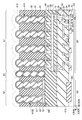
図5は、本実施形態の磁気メモリの構造例を示す断面図である。図5において、本実施形態の磁壁メモリのY方向に沿う断面(Y−Z断面)が示されている。
<Structural example>
FIG. 5 is a cross-sectional view showing a structural example of the magnetic memory of the present embodiment. In FIG. 5, a cross section (YZ cross section) of the domain wall memory of the present embodiment along the Y direction is shown.
図6は、本実施形態の磁気メモリの構造例を示す上面図(平面図)である。 FIG. 6 is a top view (plan view) showing a structural example of the magnetic memory of the present embodiment.
図5に示されるように、本実施形態の磁気メモリは、2つのチップの貼合構造を有する。 As shown in FIG. 5, the magnetic memory of the present embodiment has a two-chip bonding structure.
本実施形態において、メモリセルアレイを含むチップ(以下では、メモリセルアレイチップともよばれる)400が、メモリ制御回路CCを含むチップ(以下では、メモリ制御回路チップともよばれる)410に貼合されている。 In the present embodiment, a chip (hereinafter, also referred to as a memory cell array chip) 400 including a memory cell array is attached to a chip (hereinafter, also referred to as a memory control circuit chip) 410 containing a memory control circuit CC.
メモリセルアレイチップ400は、Z方向においてメモリ制御回路チップ410と重なる。
The memory
メモリ制御回路チップ410は、複数の電界効果トランジスタ(以下では、単にトランジスタともよばれる)TRを含む。トランジスタTRによって、磁気メモリ1のメモリセルアレイ以外の各回路110〜190が構成される。複数のトランジスタTRは、チップ410のエリア(以下では、回路エリアとよばれる)A5内に設けられる。
The memory
各トランジスタTRは、半導体基板(例えば、シリコン基板)41内のアクティブ領域AA内に、配置されている。アクティブ領域AAは、シリコン基板41内において素子分離領域(絶縁層49)によって区画された半導体領域である。
Each transistor TR is arranged in the active region AA in the semiconductor substrate (for example, a silicon substrate) 41. The active region AA is a semiconductor region partitioned by an element separation region (insulating layer 49) in the
ある導電型のウェル領域45が、アクティブ領域AA内に設けられている。トランジスタTRは、ウェル領域45に設けられている。
A
トランジスタTRのゲート電極31は、ゲート絶縁層30を介して、ウェル領域45の上方に設けられている。トランジスタTRのソース/ドレイン領域32a,32bは、ウェル領域45内に設けられている。2つのソース/ドレイン領域32a,32bは、トランジスタTRのチャネル領域を、基板41の上面に対して平行方向に挟む。ゲート電極31は、ゲート絶縁層30を介してチャネル領域に対向する。
The
トランジスタTRのゲート電極31は、シリコン基板41上の層間絶縁層39に覆われている。層間絶縁層39内に、複数のプラグ34,36、導電層(配線)35及びパッド38が、設けられている。
The
プラグ(コンタクト部)34が、ソース/ドレイン領域32(32a,32b)上に設けられている。導電層(中間配線)35が、プラグ34を介して、ソース/ドレイン領域32に接続されている。プラグ(コンタクト部)36が、導電層35上に設けられている。パッド38が、プラグ36を介して導電層35に接続されている。
A plug (contact portion) 34 is provided on the source / drain regions 32 (32a, 32b). The conductive layer (intermediate wiring) 35 is connected to the source / drain region 32 via the
例えば、メモリ制御回路チップ410は、アライメントマーク991が設けられたエリア(以下では、アライメントマークエリアとよばれる)A6を含む。アライメントマークエリアA6は、チップ410の表面に対して平行な方向において、回路エリアA5に隣り合う。
For example, the memory
メモリセルアレイチップ400が、Z方向においてメモリ制御回路チップ410の上方に設けられている。
メモリセルアレイチップ400は、上述(図3及び図4参照)の複数のメモリセルユニットMUを含む。
The memory
The memory
各メモリセルユニットMUは、磁性層51を含む。複数の磁性層51が、絶縁層61内に設けられている。
Each memory cell unit MU includes a
図5に示されるように、複数のメモリセルユニットMUが設けられた領域(以下では、メモリセルアレイエリアとよばれる)A1が、メモリセルアレイチップ(以下では、アルミナプレートともよばれる)400内に設けられている。 As shown in FIG. 5, an area (hereinafter referred to as a memory cell array area) A1 in which a plurality of memory cell units MUs are provided is provided in a memory cell array chip (hereinafter also referred to as an alumina plate) 400. ing.
メモリセルアレイエリアA1において、磁性体51は、絶縁層61内のホール910内に設けられている。例えば、絶縁層61は、アルミナ層(例えば、多孔質アルミナ層)61である。以下では、アルミナ層61内のホール910は、アルミナホール910とよばれる。
In the memory cell array area A1, the
アルミナホール910内において、磁性体51は、アルミナ層61と絶縁層62との間に設けられている。
In the
磁性体51は、Z方向に延在する。磁性体51は、筒状の形状を有する。磁性体51は、Z方向において周期的にくびれている。磁性体51のチップの表面に対して平行方向の寸法(磁性体51の径)は、Z方向に沿って周期的に変化する。
The
メモリセルアレイエリアA1内において、複数のアルミナホール910(ホール内の部材51,62)は、所定のピッチDp1で配列されている。ピッチDp1は、チップ400の表面(上面)に対して平行な方向(例えば、Y方向)における2つのアルミナホール910の中心間の間隔である。
In the memory array area A1, a plurality of alumina holes 910 (
メモリセルユニットMUの再生素子10及びスイッチング素子20は、Z方向における磁性体51とメモリ制御回路チップ410との間に設けられている。再生素子10は、磁性層59を介して、磁性体51に接続されている。再生素子10は、スイッチング素子20を介して配線71(ビット線BL)に接続されている。書き込み配線75(WRL)は、Z方向における磁性層59と配線71との間に設けられている。再生素子10、スイッチング素子20、配線71,75は、層間絶縁層69に覆われている。層間絶縁層69は、Z方向において、アルミナ層61と層間絶縁層39との間に設けられている。
再生素子10、スイッチング素子20、配線71,75は、Z方向における、メモリセルMCの下方、及び、メモリ制御回路チップ410の上方に、設けられている。
The reproduction element 10 and the switching
The reproducing element 10, the switching
複数のパッド73は、Z方向における配線71の下方に設けられている。パッド73は、メモリセルアレイチップ400内の配線(例えば、配線71)に接続されている。複数のパッド73は、メモリセルアレイチップ400の第1の面(以下では、貼合面ともよばれる)側に設けられている。
The plurality of
複数のパッド73のうち1つ以上は、メモリ制御回路チップ410のパッド38に直接接触する。パッド73を介して、メモリセルユニットMUは、メモリ制御回路チップ410内のトランジスタTR(回路)に接続される。
One or more of the plurality of
パッド73,38は、チップ400,410の貼合のためのパッド(以下では、貼合パッドとよばれる)として機能する。例えば、2つのチップ400,410は、パッド38,73間及び(又は)絶縁層39,69間の共有結合によって結合する。
The
尚、複数のパッド73のうち1つ以上は、メモリセルアレイチップ400内の構成要素に接続されていなくてもよい。複数のパッド38のうち1つ以上は、メモリ制御回路チップ410内の構成要素に接続されていなくともよい。
複数のパッド78及び配線(例えば、ワード線)70が、貼合パッド73が設けられた面の反対側の面(メモリセルアレイチップの第2の面)側に設けられている。層間絶縁層79は、メモリセルアレイチップ400の第2の面を覆っている。
配線70は、磁性体51に接続されている。配線70は、層間絶縁層79に覆われている。パッド78は、磁気メモリと他のデバイスとを接続するための外部接続端子として、機能する。パッド78は、磁気メモリ内の配線(例えば、配線70)に電気的に接続されている。
It should be noted that one or more of the plurality of
A plurality of
The
尚、メモリ制御回路チップ410に、外部接続端子(図示せず)が、設けられてもよい。
The memory
本実施形態において、アライメントマークを含む領域(以下では、アライメントマークエリアとよばれる)A2が、メモリセルアレイチップ(アルミナプレート)400の端部に設けられている。アライメントマークエリアA2は、Z方向においてメモリ制御回路チップ410のアライメントマークエリアA6に対向する。
In the present embodiment, a region including the alignment mark (hereinafter referred to as an alignment mark area) A2 is provided at the end of the memory cell array chip (alumina plate) 400. The alignment mark area A2 faces the alignment mark area A6 of the memory
アライメントマークエリアA2内において、アルミナホール910Aが、アルミナ層61内に設けられている。例えば、アライメントマークエリアA2において、メモリセルアレイエリアA1のアルミナホール910内の構成部材51,62と実質的に同じ部材が、アルミナホール910A内に設けられている。
例えば、アライメントマークエリアA2において、導電層55が、Z方向において部材51,62と重なる位置に設けられている。導電層55は、メモリセルアレイチップ400の貼合パッド73が設けられた面側に設けられている。
In the alignment mark area A2, the
For example, in the alignment mark area A2, the
マーク部(マーク部材)990が、アライメントマークエリアA2のアルミナホール910A内に設けられている。例えば、マーク部990は、磁性体51、絶縁層62及び導電層55を含む。アライメントマークAMは、1つ以上のマーク部990を用いて、形成される。
The mark portion (mark member) 990 is provided in the
本実施形態において、メモリセルアレイチップ400のアライメントマークAMを用いて、メモリセルアレイチップ400の形成時の或る工程における部材間の位置合わせ(例えば、リソグラフィ時のマスクと基板との位置合わせ)が、行われる。
メモリセルアレイチップ400のアライメントマークAM及びメモリ制御回路チップ410のアライメントマーク991を用いて、2つのチップ(ウェハ)の貼合時における位置合わせが、実行される。
In the present embodiment, the alignment mark AM of the memory
Using the alignment mark AM of the memory
アライメントマークエリアA2内において、複数のアルミナホール910A(ホール910A内の部材51,62)は、所定のピッチDp2で配列されている。ピッチDp2は、チップ400の表面(上面)に対して平行な方向(例えば、Y方向)における2つのアルミナホール910Aの中心間の間隔である。
例えば、ピッチDp2は、ピッチDp1と同じ大きさを有する。但し、ピッチD2は、ピッチD1と異なる大きさを有していてもよい。
Within the alignment mark area A2, the plurality of
For example, pitch Dp2 has the same magnitude as pitch Dp1. However, the pitch D2 may have a size different from that of the pitch D1.
例えば、メモリセルアレイチップ400において、1つ以上のアルミナホール910Xが、メモリセルアレイエリアA1とアライメントマークエリアA2との間のエリアA3内に設けられている。
For example, in the memory
図6を用いて、アライメントマークエリアの構造について、説明する。 The structure of the alignment mark area will be described with reference to FIG.
図6は、本実施形態の磁気メモリにおける、メモリセルアレイチップ(アルミナプレート)の構造例を示す上面図である。図6において、メモリセルアレイチップ400のZ方向におけるアルミナホール910,910Aが設けられた平面が示されている。
FIG. 6 is a top view showing a structural example of a memory cell array chip (alumina plate) in the magnetic memory of the present embodiment. FIG. 6 shows a flat surface of the memory
図6に示されるように、メモリセルアレイエリアA1が、メモリセルアレイチップ400内に設けられている。
As shown in FIG. 6, the memory cell array area A1 is provided in the memory
メモリセルユニットMUの磁性体51は、メモリセルアレイエリアA1内に設けられている。磁性体51は、アルミナ層61内のホール(アルミナホール)910内に設けられている。
The
アルミナホール910及び複数の磁性体51は、例えば、Z方向から見て六方格子配列で、メモリセルアレイエリアA1内に、配列されている。六方格子配列は、1つの格子を形成する構成要素が、六角形の頂点及び中心に配置されたレイアウトである。
The alumina holes 910 and the plurality of
複数のアルミナホール910及び複数の磁性体51は、或るピッチDp1で規則的に配列されている。例えば、ピッチDp1は、チップ400をZ方向から見た場合における、Y方向に隣り合う2つのアルミナホールの中心間の間隔である。
図6において、メモリセルアレイエリアA1における、Y方向におけるアルミナホール(磁性体)のピッチDp1が、示されている。但し、メモリセルアレイエリアA1内の複数のアルミナホール910に関して、X方向に並ぶ2つのアルミナホール910のピッチ、及び、X−Y平面に対して斜め方向に並ぶ2つのアルミナホール910のピッチは、所定の大きさに、それぞれ設定されている。
The plurality of
In FIG. 6, the pitch Dp1 of the alumina holes (magnetic material) in the Y direction in the memory cell array area A1 is shown. However, with respect to the plurality of
アルミナホール910は、X−Y面に対して平行な方向において、寸法Da(寸法D1から寸法D2までの間の寸法)を有する。複数のアルミナホール910Aは、実質的に同じ寸法Dbを有する。
The
アライメントマークエリアA2は、チップ400の上面に対して平行な方向においてメモリセルアレイエリアA1に隣り合うように、チップ400内に設けられている。例えば、アライメントマークエリアA2は、チップ400の上面に対して平行方向におけるメモリセルアレイエリアA1の四方を囲んでいる。アライメントマークエリアA2は、四角形のリング状のエリアである。
The alignment mark area A2 is provided in the
例えば、アライメントマークエリアA2は、メモリセルアレイチップ(アルミナプレート)400を形成するためのウェハのダイシングエリア内に設けられている。メモリセルアレイチップ400は、ウェハのダイシングによって、ウェハから切り出される。
For example, the alignment mark area A2 is provided in the dicing area of the wafer for forming the memory cell array chip (alumina plate) 400. The memory
アライメントマークエリアA2内において、複数のアルミナホール910A及び複数の磁性体51は、メモリセルアレイエリアA1内のアルミナホール910及び磁性体51と同様に例えば、Z方向から見て六方格子配列で配列されている。
In the alignment mark area A2, the plurality of
アルミナホール910A内に、磁性体51及び絶縁層62が、設けられている。アルミナホール910A内の構成部材は、アルミナホール910内の構成部材と実質的に同じである。但し、アライメントマークエリアA2内において、アライメントの精度の向上のために、導電層55が、Z方向においてアルミナホール910A(磁性体51及び絶縁層62)と重なる位置に、設けられてもよい。
A
例えば、導電層55、磁性体51及び絶縁層62が、アライメントマークのマーク部990を構成する。
For example, the
複数のアルミナホール910A及び複数の磁性体51は、或るピッチDp2(例えば、Dp2=Dp1)で規則的に配列されている。例えば、ピッチDp2は、チップ400をZ方向から見た場合における、Y方向に隣り合う2つのメモリホールの中心間の間隔である。
The plurality of
例えば、Z方向からのある位置において、X−Y面に対して平行な方向におけるアルミナホール910Aの寸法Dbは、X−Y面に対して平行な方向におけるアルミナホール910の寸法Daと同じである。
複数のアルミナホール910Aは、実質的に同じ寸法Dbを有する。
For example, at a certain position from the Z direction, the dimension Db of the
The plurality of
図6において、アライメントマークエリアA2において、Y方向におけるアルミナホール(磁性体)のピッチDp2が、示されている。但し、アライメントマークエリアA2内の複数のアルミナホール910Aに関して、X方向に並ぶ2つのアルミナホール910Aのピッチ、及び、X−Y平面に対して斜め方向に並ぶ2つのアルミナホール910Aのピッチは、所定の大きさに、それぞれ設定されている。
In FIG. 6, in the alignment mark area A2, the pitch Dp2 of the alumina holes (magnetic material) in the Y direction is shown. However, with respect to the plurality of
尚、アライメントマークエリアA2において、アルミナホール910A(埋め込み部材51,62)間のピッチDp2は、アルミナホール910間のピッチDp1と異なっていてもよい。アルミナホール910Aの寸法(埋め込み部材51,62)Dbは、アルミナホール910の寸法Daと異なってもよい。
In the alignment mark area A2, the pitch Dp2 between the
アライメントマークAMは、1つ以上のマーク部材(例えば、六方格子配列を構成する7つのマーク部材)990から形成される。 The alignment mark AM is formed from one or more mark members (for example, seven mark members constituting a hexagonal lattice arrangement) 990.
尚、アライメントマークエリアA2内において、アライメントマークAMを形成するためのアルミナホール910A以外の複数のアルミナホール910Bは、エリアA2内で所定のピッチを有さずにランダムな配置で設けられていてもよい。複数のアルミナホール910Bの寸法は、均一な寸法を有さなくともよい。
この結果として、複数のアルミナホール910B内のそれぞれの部材51B,62Bは、ランダムな配列で、エリアA2内に設けられている。複数の部材51B,62Bの寸法は、均一な寸法を有さない。
In the alignment mark area A2, a plurality of
As a result, the
例えば、エリア(以下では、中間エリアともよばれる)A3が、メモリセルアレイエリアA1とアライメントマークエリアA2との間に設けられている。中間エリアA3は、メモリセルアレイエリアA1とアライメントマークエリアA2との間で、メモリセルアレイエリアA1の周りを囲んでいる。 For example, an area (hereinafter, also referred to as an intermediate area) A3 is provided between the memory cell array area A1 and the alignment mark area A2. The intermediate area A3 surrounds the memory cell array area A1 between the memory cell array area A1 and the alignment mark area A2.
中間エリアA3は、複数のアルミナホール910Xを含む。アルミナホール910X内に、磁性体51及び絶縁層62が設けられている。
The intermediate area A3 includes a plurality of
中間エリアA3の構造は、メモリセルアレイエリアA1の構造及びアライメントマークエリアA2の構造と異なる。
中間エリアA3内において、複数のアルミナホール910Xは、六方格子配列を有さずに、ランダムな配置で、設けられている。中間エリアA3内において、アルミナホール910Xは、不規則に並んでいる。或るアルミホール910Xと他の複数のアルミナホール910Xとの間の間隔(ピッチ)に関して、各間隔は、それぞれ異なる。
The structure of the intermediate area A3 is different from the structure of the memory cell array area A1 and the structure of the alignment mark area A2.
In the intermediate area A3, the plurality of
例えば、アルミナホール910X内の部材(磁性体51及び絶縁層62)は、メモリデバイス1の構成要素としての機能を有さない。以下では、アルミナホール910X内の部材51,62は、ダミー部材ともよばれる。
For example, the members (
中間エリアA3内において、X−Y面に対して平行な方向におけるアルミナホール910Xの寸法は、アルミナホール910Xごとに異なってもよい。Z方向におけるアルミナホール910Xの寸法(アルミナホール910Xの深さ)は、アルミナホール910Xごとに異なってもよい。
In the intermediate area A3, the dimensions of the alumina holes 910X in the direction parallel to the XY plane may differ for each
以下では、所定のピッチでホールが配列されたエリアA1,A2は、規則配列エリアともよばれる。不規則にホールが配列されたエリアA3は、不規則配列エリア(又は自由配列エリア)ともよばれる。 In the following, the areas A1 and A2 in which holes are arranged at a predetermined pitch are also referred to as regular arrangement areas. The area A3 in which holes are irregularly arranged is also called an irregular arrangement area (or free arrangement area).
本実施形態の磁壁メモリにおいて、アライメントマークを形成するための部材(マーク部)が、アライメントマークエリアA2内に、所定のピッチで規則的な配列で、設けられている。マーク部は、陽極酸化によって形成されたアルミナ層のホール内に設けられている。 In the domain wall memory of the present embodiment, members (mark portions) for forming alignment marks are provided in the alignment mark area A2 in a regular arrangement at a predetermined pitch. The mark portion is provided in the hole of the alumina layer formed by anodizing.
尚、本実施形態の磁壁メモリの動作は、周知の技術によって、実行される。
例えば、磁壁メモリの読み出しシーケンスにおいて、シフト動作によって、データの読み出し対象のメモリセルのデータが、読み出しセルにシフトされる。読み出しセルにシフトされたデータが、再生素子(MTJ素子)10によって読み出される。
例えば、磁壁メモリの書き込みシーケンスにおいて、書き込みデータに応じた方向に流れる書き込み電流が、書き込み配線に供給される。書き込み配線から生じる磁場によって、書き込みセル内に、データが書き込まれる。書き込みセル内に書き込まれたデータが、シフト動作によって、データの書き込み対象のメモリセルにシフトされる。
The operation of the domain wall memory of this embodiment is executed by a well-known technique.
For example, in the domain wall memory read sequence, the shift operation shifts the data in the memory cell to which the data is read to the read cell. The data shifted to the read cell is read by the reproduction element (MTJ element) 10.
For example, in the writing sequence of the domain wall memory, the writing current flowing in the direction corresponding to the writing data is supplied to the writing wiring. Data is written into the write cell by the magnetic field generated by the write wiring. The data written in the write cell is shifted to the memory cell to which the data is written by the shift operation.
(1b)製造方法
図7乃至図15を参照して、本実施形態の磁壁メモリの製造方法について、説明する。
(1b) Manufacturing method
The method of manufacturing the domain wall memory of the present embodiment will be described with reference to FIGS. 7 to 15.
図7は、本実施形態の磁気メモリの製造方法の一工程を説明するための図である。 FIG. 7 is a diagram for explaining one step of the method for manufacturing the magnetic memory of the present embodiment.
図7に示されるように、第1のシリコン基板40(シリコンウェハ9)上に、アルミニウム層60が形成される。例えば、アルミニウム層60の膜厚は、おおよそ数μmから数百μm程度である。アルミニウムの純度が99.90%以上の高純度アルミニウムが、アルミニウム層60に用いられことが好ましい。
As shown in FIG. 7, the
アルミニウム層60は、例えば、スパッタ法、メッキ法、CVD(Chemical Vapor Deposition)法、シリコン基板40に対するアルミニウム層(アルミニウム基板、アルミニウム箔)の貼合などを用いて、形成される。
The
図7の例において、アルミニウム層60がシリコン基板40に直接接している。但し、アルミニウム層60とシリコン基板40との間に、他の材料の膜(例えば、絶縁層)が、形成されていてもよい。この場合において、アルミニウム層60が、シリコン基板40を覆う絶縁層上に形成される。
In the example of FIG. 7, the
図8及び図9は、本実施形態の磁気メモリの製造方法の一工程を説明するための図である。図8は、本実施形態の磁気メモリの製造方法の一工程を説明するための模式的な断面工程図である。図9は、図8の工程に対応する模式的な上面図(平面図)である。 8 and 9 are diagrams for explaining one step of the method for manufacturing the magnetic memory of the present embodiment. FIG. 8 is a schematic cross-sectional process diagram for explaining one step of the method for manufacturing the magnetic memory of the present embodiment. FIG. 9 is a schematic top view (plan view) corresponding to the process of FIG.
図8に示されるように、リソグラフィ(例えば、フォトリソグラフィ)によって、Z方向におけるアルミニウム層60の表面(上面)上に、レジストマスク90が形成される。レジストマスク90は、アルミニウム層60に対する陽極酸化の反応起点を形成するための複数のパターン(開口部)901を有する。
As shown in FIG. 8, a resist mask 90 is formed on the surface (upper surface) of the
図9に示されるように、レジストマスク90の複数のパターン901は、六方格子配列(六方最密配置)でレイアウトされていることが望ましい。各パターン901は、ホールパターンを有する。ホールパターン901は、Z方向から見て、円形状(楕円形状)の平面形状を有する。
As shown in FIG. 9, it is desirable that the plurality of
ホールパターン901のピッチDPは、数十nmから数百nm程度である。ピッチDPは、Y方向における2つのパターン800の中心の間隔を示す。
The pitch DP of the
例えば、ホールパターン901は、メモリセルアレイエリアA1及びアライメントマークエリア(ウェハ9のダイシングエリア)A2内に、形成されている。例えば、メモリセルアレイエリアA1とアライメントマークエリアA2との間のエリアA3内において、ホールパターン901は、形成されていない。また、アライメントマークエリアA2内のアライメントマークが配置される領域以外において、ホールパターン901は、形成されなくともよい。
For example, the
尚、リソグラフィの前に、アルミニウム層60の上面が、CMP等の平坦化処理によって、平坦化されていることが望ましい。
It is desirable that the upper surface of the
ホールパターン901を有するレジストマスク90をマスクに用いて、アルミニウム層60の上面が、ドライエッチング又はウエットエッチングによってエッチングされる。
The upper surface of the
これによって、アルミニウム層60の上面に、リセス900が形成される。リセス900の深さ(基板40の表面に対して垂直方向の寸法)Dzは、例えば、数nmから数十nm程度である。
As a result, the
エッチングによって形成されたリセス900は、アルミニウム層60の陽極酸化の反応起点となる。
このように、本実施形態において、アルミニウム層60の陽極酸化のための反応起点900が、メモリセルアレイエリアA1及びアライメントマークエリア(ダイシングエリア)A2内に、形成される。
The
As described above, in the present embodiment, the
図10は、本実施形態の磁気メモリの製造方法の一工程を説明するための模式的な断面工程図である。 FIG. 10 is a schematic cross-sectional process diagram for explaining one step of the method for manufacturing the magnetic memory of the present embodiment.
図10に示されるように、アルミニウム層に対する陽極酸化が、実行される。 As shown in FIG. 10, anodization of the aluminum layer is performed.
アルミニウム層及びシリコン基板40は、陽極酸化装置内の電解質溶液(硫酸、シュウ酸、リン酸など)891内に、浸される。
電解質溶液891中において、シリコン基板40が陽極に設定される。陽極酸化のための電圧(以下では、陽極酸化電圧とよばれる)V1が、電圧回路899からシリコン基板40に印加される。
The aluminum layer and the
In the
これによって、アルミニウム層の酸化によって、アルミナ層(酸化アルミニウム層)61が、シリコン基板40上方に形成される。
As a result, the alumina layer (aluminum oxide layer) 61 is formed above the
陽極酸化電圧V1の適正化によって、あらかじめ形成された反応起点(リセス)900のピットと実質的に同じピッチDp1,Dp2でシリコン基板40の上面に対して垂直な方向(Z方向)に延在するホール(アルミナホール)910,910Aが、アルミナ層61(又はアルミニウム層60)内に形成される。 By optimizing the anodizing voltage V1, the pitches Dp1 and Dp2, which are substantially the same as the pits of the reaction starting point (recess) 900 formed in advance, extend in the direction perpendicular to the upper surface of the silicon substrate 40 (Z direction). Holes (alumina holes) 910 and 910A are formed in the alumina layer 61 (or aluminum layer 60).
アルミニウム層に対する陽極酸化中において、陽極酸化電圧V1の大きさが、周期的に(所定の時間の間隔で)変調されてもよい。これによって、陽極酸化電圧V1の大小に応じて、アルミナホール910,910Aに周期的なくびれ(凹部)519が生じる。この結果として、くびれ構造を有するアルミナホール910,910Aが、形成され得る。アルミナホール910は、球形の空間がZ方向に連なった構造を有する。
During anodizing the aluminum layer, the magnitude of the anodizing voltage V1 may be modulated periodically (at intervals of predetermined time). As a result, periodic constrictions (recesses) 519 are formed in the alumina holes 910 and 910A depending on the magnitude of the anodizing voltage V1. As a result, alumina holes 910,910A having a constricted structure can be formed. The
また、陽極酸化の時間の調整によって、アルミナホール910の深さ(Z方向における寸法)が、所望の大きさに調整され得る。これによって、アルミナホール910,910Aの下部に、未反応のアルミニウム層60Aが、残存されてもよい。
例えば、アルミニウム層60Aが、シリコン基板40上の絶縁層上に形成されている場合がある。アルミニウム層60Aの残存によって、シリコン基板40とアルミニウム層60Aとの間に絶縁層が存在していたとしても、アルミニウム層を電極として用いることで、陽極酸化電圧V1が、未反応のアルミニウム層60Aを介して、基板の外周部から基板の中心部までのアルミニウム層に供給され得る。
Further, the depth (dimension in the Z direction) of the
For example, the
陽極酸化によってZ方向に延在するアルミナホール910,910Aが形成される場合、アルミナバリア層619が、アルミナホール910,910Aの底部に形成される。
When the alumina holes 910 and 910A extending in the Z direction are formed by anodizing, the
このように、アルミニウム層に対する陽極酸化における反応起点の形成及び陽極酸化電圧の制御によって、形成されるアルミナホールの形状が、制御される。
したがって、メモリセルアレイエリアA1及びアライメントマークエリアA2において、規則的な配列(例えば、所定のピッチDp1,Dp2)を有する複数のアルミナホール910,910Aが、形成される。
In this way, the shape of the formed alumina holes is controlled by the formation of the reaction starting point in the anodizing of the aluminum layer and the control of the anodizing voltage.
Therefore, in the memory cell array area A1 and the alignment mark area A2, a plurality of
例えば、中間エリアA3内において、アルミナホール910Xが、アルミナホール910と同時に形成される。アルミナホール910Xは、反応起点(リセス)900無しに、アルミナ層61内に形成される。
それゆえ、中間エリアA3内のアルミナホール910Xは、エリアA1,A2内のアルミナホール910とは異なって、ランダムな配列でエリアA3内に形成される。また、中間エリアA3内の複数のアルミナホール910Xにおいて、アルミナホール910Xの深さは、ばらつく場合がある。
For example, in the intermediate area A3, the alumina holes 910X are formed at the same time as the alumina holes 910. The
Therefore, the alumina holes 910X in the intermediate area A3 are formed in the area A3 in a random arrangement unlike the alumina holes 910 in the areas A1 and A2. Further, in the plurality of
図11は、本実施形態の磁気メモリの製造方法の一工程を説明するための模式的な断面工程図である。 FIG. 11 is a schematic cross-sectional process diagram for explaining one step of the method for manufacturing the magnetic memory of the present embodiment.
図11に示されるように、メモリセルアレイエリアA1及びアライメントマークエリアA2において、磁性体(磁性層)51が、CVD法又はALD(Atomic layer deposition)法を用いて、アルミナホール910,910A内に形成される。例えば、形成された磁性体51は、アルミナホール910,910A内において、筒状の構造を有する。
As shown in FIG. 11, in the memory cell array area A1 and the alignment mark area A2, the magnetic material (magnetic layer) 51 is formed in the alumina holes 910 and 910A by using the CVD method or the ALD (Atomic layer deposition) method. Will be done. For example, the formed
形成された磁性体51は、アルミナホール910,910Aの形状に依存した構造を有する。
上述のように、アルミナホール910,910Aが周期的なくびれを有する場合、磁性体51は、周期的にくびれた構造を有する。磁性体51は、Z方向における或る間隔でくびれ部(凹部)519を有する。磁性体51において、磁性体51の外周側へ突出した凸部511が、Z方向に並ぶ凹部519間に設けられている。このように、くびれ構造の磁性体51において、凸部511と凹部519とが、Z方向に交互に並ぶように、アルミナホール910,910A内に形成される。
The formed
As described above, when the alumina holes 910 and 910A have a periodic constriction, the
絶縁体(例えば、酸化シリコン層)62が、CVD法、ALD法又は塗布法などによって、筒状の磁性層51の空隙内に、埋め込まれる。
The insulator (for example, the silicon oxide layer) 62 is embedded in the voids of the cylindrical
中間エリアA3内において、磁性体及び絶縁体が、エリアA1,A2内における磁性体51及び絶縁層62の形成と共通の工程によって、アルミナホール(図示せず)内に形成される。中間エリアA3において、複数の磁性体(及び絶縁体)は、不規則なピッチで配列されている。中間エリアA3内の複数の磁性体51の形状は、不均一に形成される。
In the intermediate area A3, the magnetic material and the insulator are formed in the alumina holes (not shown) by the same process as the formation of the
例えば、アライメントマークエリアA2内において、アルミナホール910内の磁性体51の上部が、エッチングによって除去される。これによって、リセスが、エリアA2内のアルミナ層61の上面に、形成される。導電層(例えば、金属層)55が、磁性体51の上方のリセス内に、形成される。
For example, in the alignment mark area A2, the upper part of the
図12は、本実施形態の磁気メモリの製造方法の一工程を説明するための模式的な断面工程図である。 FIG. 12 is a schematic cross-sectional process diagram for explaining one step of the method for manufacturing the magnetic memory of the present embodiment.
図12に示されるように、周知の技術によって、メモリセルユニットの構成素子10,20,59、複数の配線71,75及び層間絶縁膜68などが、アルミナ層61の第1の面の上方に形成される。
As shown in FIG. 12, by a well-known technique, the
例えば、複数の磁性層59が、周知の技術によって、アルミナ層61の上面上に形成される。各磁性層59は、対応する磁性体51に接続される。磁性層59の上方に、書き込み配線75が、形成される。
For example, a plurality of
再生素子(例えば、MTJ素子)10が、Z方向において磁性層59の上面上に形成される。スイッチング素子20が、Z方向において再生素子10上に形成される。
A reproducing element (for example, an MTJ element) 10 is formed on the upper surface of the
ビット線71が、スイッチング素子20に接続されるように、アルミナ層61の上方に形成される。複数のパッド(例えば、貼合パッド)73が、ビット線71の上方に形成される。
The
構成素子10,20,59,71,75の各部材のパターニングのために、リソグラフィ(例えば、フォトリソグラフィ)が実行される。本実施形態において、このリソグラフィのためのマスクと基板40(ウェハ9)との位置合わせは、陽極酸化時に形成されたアライメントマークAMを用いて、実行される。
Lithography (eg, photolithography) is performed to pattern each member of the
図13は、本実施形態の磁気メモリの製造方法の一工程を説明するための模式的な断面工程図である。 FIG. 13 is a schematic cross-sectional process diagram for explaining one step of the method for manufacturing the magnetic memory of the present embodiment.
図13に示されるように、メモリ制御回路(CMOS回路)CCが、周知の技術によって、第2のシリコン基板41(ウェハ9A)の回路エリアA5内に形成される。例えば、トランジスタTRのゲート絶縁層30及びゲート電極31が、シリコン基板41のアクティブ領域AA(ウェル領域45)上に形成される。トランジスタTRのソース/ドレイン領域32が、ウェル領域45内に形成される。
プラグ36及び配線が、トランジスタTRを覆う層間絶縁膜39内に形成される。
パッド38が、第2のシリコン基板41の上面の上方に形成される。
As shown in FIG. 13, a memory control circuit (CMOS circuit) CC is formed in the circuit area A5 of the second silicon substrate 41 (wafer 9A) by a well-known technique. For example, the gate insulating layer 30 and the
The
The
例えば、アライメントマーク991が、シリコン基板41(ウェハ)のアライメントマークエリア(ダイシングエリア)A6内に、形成されている。
For example, the
尚、メモリ制御回路CCの形成のためのプロセスは、メモリセルアレイ100の形成のためのプロセスと並行に実行されてもよいし、メモリセルアレイ100の形成のためのプロセスの前又は後に形成されてもよい。
The process for forming the memory control circuit CC may be executed in parallel with the process for forming the
2つのシリコン基板40,41が、貼合される。2つのシリコン基板(シリコンウェハ)40,41の上面(以下では、貼合面とよばれる)同士が、接着される。
Two
シリコン基板40,41の貼合時において、一方のシリコン基板40のパッド(例えば、貼合パッド)73が、他方のシリコン基板41のパッド(例えば、貼合パッド)38に対向するように、一方のシリコン基板40が、他方のシリコン基板41に貼り合わせられる。
例えば、Z方向においてシリコン基板41がシリコン基板40の下方に位置するように、貼合パッド73が、貼合パッド38に接着される。2つのシリコン基板40,41は、パッド73,38間に生じる共有結合(及び層間絶縁層68,39間に生じる共有結合)によって、結合される。
At the time of bonding the
For example, the
例えば、本実施形態において、シリコン基板40,41の貼合時におけるシリコン基板40,41間の位置合わせは、アルミナ層61内に設けられたアライメントマークAMとシリコン基板41内のアライメントマーク991とを用いて、実行される。
For example, in the present embodiment, the alignment mark AM provided in the
図14は、本実施形態の磁気メモリの製造方法の一工程を説明するための模式的な断面工程図である。 FIG. 14 is a schematic cross-sectional process diagram for explaining one step of the method for manufacturing the magnetic memory of the present embodiment.
図14に示されるように、貼り合わせた2つのシリコン基板40,41の上部側(ここでは、第1のシリコン基板40の裏面側)のシリコンが、バックグラインドのような研磨技術を用いて、除去される。これによって、未反応のアルミニウム層60Aが、露出する。シリコン基板(ウェハ)41が、薄くされた基板40を支持する。
As shown in FIG. 14, the silicon on the upper side (here, the back surface side of the first silicon substrate 40) of the two bonded
エッチング(例えば、ウェットエッチング)によって、未反応のアルミニウム層60Aが除去される。これによって、Z方向における磁性体51の上方のアルミナバリア層619(アルミナホール910の底部)が、露出する。
The
図15は、本実施形態の磁気メモリの製造方法の一工程を説明するための模式的な断面工程図である。 FIG. 15 is a schematic cross-sectional process diagram for explaining one step of the method for manufacturing the magnetic memory of the present embodiment.
図15に示されるように、例えば、リン酸を用いたウエットエッチングによって、露出したアルミナバリア層619がエッチングされる。これによって、アルミナホール910,910A内の磁性体51が、露出する。
As shown in FIG. 15, the exposed
図16は、本実施形態の磁気メモリの製造方法の一工程を説明するための模式的な断面工程図である。 FIG. 16 is a schematic cross-sectional process diagram for explaining one step of the method for manufacturing the magnetic memory of the present embodiment.
図16に示されるように、磁性体51及び絶縁層62に対して、CMPによる平坦化処理が、実行される。この時、アルミナ層61をストッパ層に用いて、磁性体51と絶縁層62とが研磨される。
As shown in FIG. 16, the
この後、図5に示されるように、磁性層51に接続されるように、電極、素子、配線及びパッド等の磁気メモリの構成部材が、周知の技術によって形成される。例えば、X方向に延在する配線(例えば、ワード線WL)が、磁性体51に接続されるように、アルミナ層61の第2の面上に形成される。配線70を覆うように層間絶縁層79が、アルミナ層61上に形成される。層間絶縁層79内に、複数のパッド(外部接続端子)78が形成される。パッド78は、層間絶縁層68,79内の配線70,71,75などに接続される。
After that, as shown in FIG. 5, constituent members of the magnetic memory such as electrodes, elements, wirings, and pads are formed by a well-known technique so as to be connected to the
配線70及びパッド78の形成時において、メモリセルアレイチップ400のアライメントマークAMが、リソグラフィのマスクとウェハとの位置合わせのために、用いられてもよい。
At the time of forming the
これによって、本実施形態の磁壁メモリ1が、メモリ制御回路チップ(ウェハ)41を支持基板として形成される。 As a result, the domain wall memory 1 of the present embodiment is formed with the memory control circuit chip (wafer) 41 as a support substrate.
この後、ウェハのダイシングによって、本実施形態の磁壁メモリ1が、チップ化される。この時、ダイシングエリア内のアライメントマークエリアA2のアライメントマークの一部又は全ては切断され、アライメントマークは、磁壁メモリのチップから除去される場合もある。 After that, the domain wall memory 1 of the present embodiment is made into a chip by dicing the wafer. At this time, a part or all of the alignment mark in the alignment mark area A2 in the dicing area may be cut, and the alignment mark may be removed from the chip of the domain wall memory.
以上のように、本実施形態の磁気メモリが、完成する。 As described above, the magnetic memory of the present embodiment is completed.
(c)まとめ
本実施形態において、磁気メモリは、2つのチップが貼り合わされた構造を有する。
本実施形態において、メモリセルアレイチップを形成するためのシリコン基板(ウェハ)に対するバックグラインド工程の後に実行される複数の工程において、メモリ制御回路チップを形成するための基板が、バックグライドされたメモリセルアレイチップに対する支持基板となる。
そのため、本実施形態において、大口径のウェハが基板に用いられた場合であっても、基板のハンドリングの問題は、生じない。
(C) Summary
In the present embodiment, the magnetic memory has a structure in which two chips are bonded together.
In the present embodiment, in a plurality of steps executed after the back grind step on the silicon substrate (wafer) for forming the memory cell array chip, the substrate for forming the memory control circuit chip is back glide memory cell array. It serves as a support substrate for the chip.
Therefore, in the present embodiment, even when a large-diameter wafer is used as the substrate, the problem of handling the substrate does not occur.
本実施形態の磁気メモリにおいて、メモリ部としての磁性体51は、絶縁層61内に形成されたホール910内に設けられている。ホール910は、アルミニウム層に対する陽極酸化によって形成される。
本実施形態の磁気メモリにおいて、磁気メモリを形成するための各種の工程において、アライメントマークAMが用いられる。
In the magnetic memory of the present embodiment, the
In the magnetic memory of the present embodiment, the alignment mark AM is used in various steps for forming the magnetic memory.
一般的なアライメントマークは、基板(ウェハ)の表面に対するリソグラフィ工程と同時に形成されたレジストパターンが、ドライエッチングを用いて、基板に転写されることで、形成される。
一方、ホールの形成のための陽極酸化がウェハ上のアルミニウム層に対して実行される場合、例えば、アライメントマークがアルミニウム層60の表面に或る材料を用いて陽極酸化の実行前に形成されたとしても、陽極酸化時における、アライメントマークの近傍のアルミニウムがアルミナに変化する時の体積膨張に起因して、アライメントマークの形状が、変形してしまう。そのため、陽極酸化工程を経たアライメントマークの使用は、好ましくない。
A general alignment mark is formed by transferring a resist pattern formed at the same time as a lithography process on the surface of a substrate (wafer) to the substrate by using dry etching.
On the other hand, if anodizing for the formation of holes is performed on the aluminum layer on the wafer, for example, alignment marks were formed on the surface of the
アルミニウム層内における陽極酸化の反応起点(リセス)を形成するための工程(例えば、レジストマスクのフォトリソグラフィ工程)において、リソグラフィ工程のためのアライメントマークが形成されることが、望ましい。 In a step for forming a reaction origin (recess) of anodization in an aluminum layer (for example, a photolithography step of a resist mask), it is desirable that an alignment mark for the lithography step is formed.
本実施形態において、アライメントマークAMを形成する部材は、陽極酸化によって形成された層61のホール910A内に、設けられている。
本実施形態において、図6、図8乃至図12に示されるように、アライメントマークAMが形成された領域A2と形成されない領域A3とが、メモリセルアレイチップ内に作り分けられる。アライメントマークAMのパターン990は、例えば、メモリ部(例えば、磁性体)を形成するためのホールパターンと同じホールパターンを用いて、形成される。
In the present embodiment, the member forming the alignment mark AM is provided in the
In the present embodiment, as shown in FIGS. 6, 8 to 12, a region A2 in which the alignment mark AM is formed and a region A3 in which the alignment mark AM is not formed are formed separately in the memory cell array chip. The
本実施形態において、アライメントマークAMは、六方格子配列の複数のホール910A内のマーク部990を、アライメントマークエリアA2内に含む。
In the present embodiment, the alignment mark AM includes the
アライメントマークエリアA2内において、陽極酸化によって、メモリ部を形成するためのアルミナホール(ホールパターン)910と同様に、配列制御されたアルミナホール910Aが、アライメントマークAMの配置のために、形成されている。
In the alignment mark area A2, array-controlled
アライメントマーク(及びメモリセルユニット)が配置されていないエリアA3内において、所定の配列を有するアルミナホールは、形成されていない。例えば、エリアA3内において、複数のアルミナホール910Xは、配列制御されていない状態(自然配列状態)で、アルミナ層61内に形成されている。
In the area A3 where the alignment mark (and the memory cell unit) is not arranged, the alumina hole having a predetermined arrangement is not formed. For example, in the area A3, the plurality of
この場合において、本実施形態によれば、複数の領域A2,A3(及び領域A1)で、アルミニウムの陽極酸化が生じるため、体積膨張によるアライメントマークの変形を、防止できる。 In this case, according to the present embodiment, since aluminum is anodized in the plurality of regions A2 and A3 (and regions A1), deformation of the alignment mark due to volume expansion can be prevented.
本実施形態において、このように形成されたアライメントマークの検出によって、スイッチング素子及び再生素子(書き込み素子又は読み出し素子)などの構成要素が、Z方向においてメモリセルアレイエリア内のアルミナホールの位置と重なる位置に、リソグラフィで形成されることが可能となる。 In the present embodiment, by detecting the alignment mark formed in this way, the components such as the switching element and the reproducing element (writing element or reading element) overlap with the position of the alumina hole in the memory cell array area in the Z direction. In addition, it can be formed by lithography.
本実施形態によれば、チップの貼合面の反対の面に、磁性層に接続される電極がリソグラフィで形成される場合において、陽極酸化に用いられるアルミニウム層は、チップの貼合面の反対の面に存在せずに、アライメントのための照明光が透過可能なアルミナ層へ、変化している。 According to the present embodiment, when the electrode connected to the magnetic layer is formed by lithography on the opposite surface of the bonding surface of the chip, the aluminum layer used for anodizing is the opposite of the bonding surface of the chip. It has changed to an alumina layer that does not exist on the surface of the surface and allows the illumination light for alignment to pass through.
それゆえ、本実施形態において、形成されたアライメントマークは、チップの貼合面の反対の面側から検出できる。その結果として、アルミナホール内のマーク部を用いて位置合わせを行うリソグラフィによって、電極が、チップの貼合面の反対の面側に形成できる。 Therefore, in the present embodiment, the formed alignment mark can be detected from the side opposite to the bonding surface of the chip. As a result, electrodes can be formed on the opposite side of the chip bonding surface by lithography that aligns using the mark portion in the alumina hole.
以上のように、本実施形態において、アライメントマークの形状の変化は、生じない。その結果として、本実施形態によれば、磁気メモリの製造工程においける位置合わせの精度は、向上する。 As described above, in the present embodiment, the shape of the alignment mark does not change. As a result, according to the present embodiment, the accuracy of alignment in the manufacturing process of the magnetic memory is improved.
尚、アライメントマークだけでなく、例えば、陽極酸化工程の後に実行される、リソグラフィ層との間のオーバーレイを測定するためのマークなども、アライメントマークの形成と実質的に同じ処理で形成されてもよい。 It should be noted that not only the alignment mark but also, for example, a mark for measuring the overlay with the lithography layer, which is executed after the anodizing step, may be formed by substantially the same process as the formation of the alignment mark. good.
陽極酸化よって酸化される層の膜厚が厚くなる場合、アルミナホールの深い部分(Z方向において反応起点の反対側の部分)において、ホールの形成の直進性が失われる場合がある。このため、アルミナホールの配列が制御された領域A2とアルミナホールの配列が制御されない領域A3との境界が、不明確になる恐れがある。 When the film thickness of the layer oxidized by anodization becomes thick, the straightness of hole formation may be lost in the deep portion of the alumina hole (the portion opposite to the reaction starting point in the Z direction). Therefore, the boundary between the region A2 in which the arrangement of the alumina holes is controlled and the region A3 in which the arrangement of the alumina holes is not controlled may become unclear.
本実施形態において、アライメントマークエリア領域(規則配列領域)A2と領域(自然配列領域)A3との境界が比較的明確なアルミナホールの表面側(貼合面側、反応起点の形成面側)において、アルミナと異なる材料(例えば、金属のような比較的高い反射率を有する材料)が埋め込まれてもよい。
これによって、本実施形態において、より高精度の位置合わせを実現することができる。
In the present embodiment, on the surface side (bonding surface side, reaction starting point forming surface side) of the alumina hole where the boundary between the alignment mark area region (regular arrangement region) A2 and the region (natural arrangement region) A3 is relatively clear. , A material different from alumina (eg, a material having a relatively high reflectance such as metal) may be embedded.
Thereby, in the present embodiment, more accurate alignment can be realized.
以上のように、本実施形態のメモリデバイス及びメモリデバイスの製造方法、製造工程の信頼性を向上できる。本実施形態のメモリデバイス及びメモリデバイスの製造方法は、形成されるデバイスの製造歩留まりを、向上できる。 As described above, the reliability of the memory device of the present embodiment, the manufacturing method of the memory device, and the manufacturing process can be improved. The memory device of the present embodiment and the method of manufacturing the memory device can improve the manufacturing yield of the formed device.
(2)第2の実施形態
図17乃至25を参照して、第2の実施形態のメモリデバイス及びメモリデバイスの製造方法について、説明する。
(2) Second embodiment
The memory device of the second embodiment and the method of manufacturing the memory device will be described with reference to FIGS. 17 to 25.
(2a)構造例
図17は、本実施形態のメモリデバイスの構成例を示すブロック図である。
(2a) Structural example
FIG. 17 is a block diagram showing a configuration example of the memory device of the present embodiment.
本実施形態のメモリデバイスは、半導体メモリである。 The memory device of this embodiment is a semiconductor memory.
図17に示されるように、本実施形態の半導体メモリは、メモリセルアレイ100A及びメモリ制御回路(CMOS回路)CCAを含む。
As shown in FIG. 17, the semiconductor memory of this embodiment includes a
本実施形態において、半導体メモリデバイスは、DRAM(Dynamic random access memory)である。 In the present embodiment, the semiconductor memory device is a DRAM (Dynamic random access memory).
本実施形態のDRAM1Aにおいて、メモリセルアレイ100Aの構成は、第1の実施形態の磁壁メモリのメモリセルアレイの構成と異なる。
In the
メモリセルアレイ100Aは、複数のメモリセルMCA、複数のワード線WL及び複数のビット線BLを含む。各メモリセルMCAは、少なくとも1つのワード線WL及び少なくとも1つのビット線BLに接続される。メモリセルMCAは、1ビット以上のデータを、格納できる。
DRAM1Aの各メモリセルMCは、電界効果トランジスタ(以下では、セルトランジスタともよばれる)、及び容量素子(以下では、セルキャパシタともよばれる)を含む。
The
Each memory cell MC of the
本実施形態のDRAM1Aは、メモリ制御回路(CMOS回路)CCAとして、ロウ制御回路110、カラム制御回路120、読み出し/書き込み回路145及びI/O回路170及び制御回路190などを含む。
The
ロウ制御回路110及びカラム制御回路は、第1の実施形態と実施的に同様に、アドレスADRに応じて、メモリセルアレイ100Aのロウ(例えば、ワード線)及びカラムの制御を行う。これによって、ワード線WLの選択及び非選択(活性化/非活性化)、ビット線BLの選択及び非選択(活性化/非活性化)、ワード線WL及びビット線BLに対する電圧の供給などが、実行される。
The
読み出し/書き込み回路145は、メモリセルアレイ100Aに対するデータの書き込み(書き込み動作)、及び、メモリセルアレイ100Aからのデータの読み出し(読み出し動作)を、行う。データの書き込み時において、読み出し/書き込み回路145は、書き込みデータに応じた信号(電圧又は電流)を、カラム制御回路120を介して、メモリセルアレイ100Aに送る。データの読み出し時において、読み出し/書き込み回路145は、読み出しデータとよばれるに応じた信号(電圧又は電流)を、カラム制御回路120を介して、メモリセルアレイ100Aから受ける。尚、データの書き込みのための回路とデータの読み出しのための回路とが、互いに独立に、DRAM1A内に設けられてもよい。
The read /
I/O回路(入出力回路)170は、外部デバイス(例えば、プロセッサ)2からのコマンドCMD、アドレスADR、データ(例えば、書き込みデータ)DT及び複数の制御信号CNTなどを受ける。I/O回路170は、制御信号CNT及びデータ(例えば、読み出しデータ)DTを、DRAM1Aの外部へ送る。
The I / O circuit (input / output circuit) 170 receives a command CMD, an address ADR, a data (for example, write data) DT, a plurality of control signal CNTs, and the like from an external device (for example, a processor) 2. The I /
制御回路190は、コマンドCMD及び制御信号CNTに基づいて、DRAM1Aの実行すべき動作に応じて、他の回路110,120,145,170の制御を行う。メモリデバイス1AがDRAMである場合、制御回路190は、データの書き込み及びデータの読み出しに加えて、メモリセルアレイ100A内のデータのリフレッシュ(リフレッシュ動作)を、制御及び実行する。
The
例えば、制御回路190は、クロック信号CLKに同期したタイミングで回路110〜170の制御を行う。この結果として、データの書き込み及びデータの読み出しは、クロック信号CLKに同期したタイミングで、実行される。クロック信号CLKは、DRAM1Aの内部で生成される、又は、外部デバイス2から供給される。
For example, the
尚、DRAM1Aは、リフレッシュ制御回路、クロック生成回路及び内部電圧生成回路などを、さらに含んでもよい。
The
<メモリセルアレイ>
図18は、本実施形態のメモリデバイスのメモリセルアレイの構成例を説明するための等価回路図である。
上述のように、メモリセルアレイ100Aは、複数のメモリセルMCdを含む。
複数のメモリセルMCdは、メモリセルアレイ100AにおけるX−Y平面内にマトリックス状に配置される。
<Memory cell array>
FIG. 18 is an equivalent circuit diagram for explaining a configuration example of a memory cell array of the memory device of the present embodiment.
As described above, the
The plurality of memory cells MCd are arranged in a matrix in the XY plane in the
メモリセルMCdの一方の端子(一端)は、ビット線BLに接続されている。
メモリセルMCdの他方の端子(他端)は、プレート線(プレート電極)PLに接続されている。
メモリセルMCdの制御端子は、ワード線WLに接続されている。
One terminal (one end) of the memory cell MCd is connected to the bit line BL.
The other terminal (the other end) of the memory cell MCd is connected to the plate wire (plate electrode) PL.
The control terminal of the memory cell MCd is connected to the word line WL.
X方向に配列された複数のメモリセルMCAは、或るワード線WLに共通に接続される。Y方向に配列された複数のメモリセルMCAは、或るビット線BLに共通に接続される。ある制御単位の複数のメモリセルMCAは、共通のプレート線PLに接続される。 A plurality of memory cells MCA arranged in the X direction are commonly connected to a certain word line WL. A plurality of memory cells MCA arranged in the Y direction are commonly connected to a certain bit line BL. A plurality of memory cells MCA of a certain control unit are connected to a common plate wire PL.
上述のように、メモリセルMCdは、セルキャパシタ80とセルトランジスタ81とを含む。
セルキャパシタ80は、1ビット以上のデータに関連付けられた電荷量を、保持する。セルキャパシタ80は、メモリセルMCのメモリ素子として機能する。
セルトランジスタ81は、メモリセルMCdとビット線BLとの接続を、スイッチングする。セルトランジスタ81は、メモリセルMCdの選択素子として機能する。
As described above, the memory cell MCd includes a
The
The
セルトランジスタ81の一方の端子(一方のソース/ドレイン)は、メモリセルMCdの端子として、ビット線BLに接続されている。
セルトランジスタ81の他方の端子(他方のソース/ドレイン)は、ノードNDを介して、セルキャパシタ80の一方の端子(一端)に接続されている。
One terminal (one source / drain) of the
The other terminal (the other source / drain) of the
セルキャパシタ80の他方の端子(他端)は、メモリセルMCdの端子として、プレート線PLに接続されている。
セルトランジスタ81のゲートは、ワード線WLに接続される。セルトランジスタ81のゲートは、メモリセルMCdの制御端子となる。
The other terminal (the other end) of the
The gate of the
図19は、本実施形態のDRAMにおける、メモリセルの構造例を示す鳥瞰図である。 FIG. 19 is a bird's-eye view showing a structural example of a memory cell in the DRAM of the present embodiment.
図19に示されるように、本実施形態において、セルトランジスタ81が、Z方向においてセルキャパシタ80と重なる。Z方向は、X−Y平面に対して垂直な方向である。Z方向は、X方向及びY方向に交差する。
As shown in FIG. 19, in this embodiment, the
セルキャパシタ80は、2つの電極801,803と、絶縁層802とを少なくとも含む。絶縁層(以下では、キャパシタ絶縁層ともよばれる)802は、2つの電極(以下では、キャパシタ電極ともよばれる)801,803間に設けられている。
The
一方のキャパシタ電極801は、プレート線PLに電気的に接続される。他方のキャパシタ電極801は、セルトランジスタ81のソース/ドレインに接続される。キャパシタ電極803とプレート線PLとの間に、キャパシタ絶縁層802とキャパシタ電極801とが設けられている。それゆえ、キャパシタ電極803は、プレート線PLに直接接触しない。
One
セルトランジスタ81は、半導体層810、ゲート絶縁層811及びゲート電極812を少なくとも含む。半導体層(以下では、チャネル層、ボディ部ともよばれる)810は、Z方向に延びる柱状の構造を有する。ゲート電極812は、ゲート絶縁層811を介して、柱状の半導体層810の側面に対向する。ゲート絶縁層811は、半導体層810の側面とゲート電極812との間に設けられている。
The
セルトランジスタ81のチャネル領域は、半導体層810内に設けられる。セルトランジスタ81の2つのソース/ドレイン領域は、半導体層810内に設けられる。以下では、柱状の半導体層810は、半導体ピラー(又はチャネルピラー)ともよばれる。
The channel region of the
本実施形態において、セルトランジスタ81は、縦型トランジスタである。
In the present embodiment, the
2つのソース/ドレイン領域のうち一方は、Z方向における半導体層810の一端(上部)側に設けられ、2つのソース/ドレイン領域のうち他方は、Z方向における半導体層810の他端(底部)側に設けられている。縦型のトランジスタ81の2つのソース/ドレインは、Z方向に並ぶ。2つのソース/ドレイン領域のうち一方は、Z方向において、2つのソース/ドレイン領域のうち他方の上方に配置されている。
セルトランジスタ81の上部側のソース/ドレイン領域は、ビット線BLに接続される。セルトランジスタ81の下部側のソース/ドレイン領域は、キャパシタ電極803に接続される。
One of the two source / drain regions is provided on one end (top) side of the
The source / drain region on the upper side of the
このように、縦型セルトランジスタ81の電流経路は、Z方向に沿う。セルトランジスタ81は、Z方向に電流を流す。
As described above, the current path of the
本実施形態において、セルトランジスタ81は、GAA(Gate all around)構造のゲート構造を有する。GAA構造のセルトランジスタ81に関して、ゲート電極812は、半導体層810内のチャネル領域の側面全体にオーバーラップする。ゲート電極812は、ゲート絶縁層811を介して、チャネル領域の側面(Z方向に沿う面)を円環状に覆う。これによって、セルトランジスタ81は、高いゲート静電制御力を有する。
In the present embodiment, the
本実施形態において、セルキャパシタ80は、アルミナ層61のアルミナホール内に設けられている。
In the present embodiment, the
<構造例>
図20は、本実施形態のDRAMの構造例を示す断面図である。図20において、DRAM1dのY方向に沿う断面(Y−Z平面)が、示されている。
<Structural example>
FIG. 20 is a cross-sectional view showing a structural example of the DRAM of the present embodiment. In FIG. 20, a cross section (YZ plane) of the DRAM 1d along the Y direction is shown.
図20に示されるように、本実施形態のDRAM1Aは、第1の実施形態の磁気メモリと同様に、複数のチップ400A,410の貼合構造を有する。
メモリセルアレイチップ400Aは、メモリセルアレイチップ400A内に設けられたパッド73とメモリ制御回路チップ410に設けられたパッド38とによって、メモリ制御回路CCAに電気的に接続されている。
As shown in FIG. 20, the
The memory
第1の実施形態と同様に、メモリ制御回路CCAは、シリコン基板41上に設けられている。メモリセルアレイチップ400Aは、Z方向においてメモリ制御回路チップ410Aの上方に設けられている。
Similar to the first embodiment, the memory control circuit CCA is provided on the
メモリセルアレイチップ400Aは、アルミナ層61を含む。アルミナ層61は、Z方向において基板(メモリ制御チップ)と重なる。
The memory
セルキャパシタ80は、アルミナ層61内に設けられている。セルトランジスタ81は、Z方向において、アルミナ層61の下方に設けられている。セルトランジスタ81は、Z方向においてセルキャパシタ80とメモリ制御回路CCAとの間に、配置されている。
The
アルミナ層61は、複数のアルミナホール911,911Aを有する。本実施形態において、アルミナホール911,911Aは、X方向(又はY方向)から見て四角形状の断面構造を有する。但し、本実施形態において、アルミナホール911,911Aは、第1の実施形態と同様に、くびれ構造を有していてもよい。
The
上述の第1の実施形態に示される例(例えば、図6参照)と同様に、複数のメモリセルMCdは、六方格子配列のレイアウト(パターン)によって、メモリセルアレイ100AのX−Y平面内に配列される。六方格子配列の1つの単位内に含まれる7つのメモリセルMCdのレイアウトに関して、6つのメモリセルMCdは、六角形の頂点にそれぞれ配置され、残りの1つのメモリセルMCdは、六角形の中央に配置される。
セルキャパシタ80(アルミナホール911)は、六方格子配列のレイアウトで、アルミナ層(アルミナプレート)61内に配列されている。
Similar to the example shown in the first embodiment described above (see, for example, FIG. 6), the plurality of memory cells MCd are arranged in the XY plane of the
The cell capacitors 80 (alumina holes 911) are arranged in the alumina layer (alumina plate) 61 in a hexagonal lattice arrangement layout.
尚、六方格子配列の複数のメモリセルにおいて、Y方向に隣り合う2つのワード線WLのそれぞれに接続された複数のメモリセルMCに関して、一方のワード線WLに接続されたメモリセルMCは、他方のワード線WLに接続されたメモリセルMCdに、Y方向(及びX方向)に対して斜め方向に並ぶ。
Y方向において或るワード線の一端側に隣り合うワード線及び他端側に隣り合うワード線に関して、一端側に隣り合うワード線に接続されたメモリセルは、他端側に隣り合うワード線に接続されたメモリセルと同じビット線に接続され、Y方向において同一直線状に配置されている。
In a plurality of memory cells in a hexagonal lattice arrangement, with respect to a plurality of memory cell MCs connected to each of two adjacent word line WLs in the Y direction, the memory cell MC connected to one word line WL is the other. The memory cells MCd connected to the word line WL are arranged diagonally with respect to the Y direction (and the X direction).
Regarding a word line adjacent to one end side of a certain word line and a word line adjacent to the other end side in the Y direction, a memory cell connected to the word line adjacent to one end side becomes a word line adjacent to the other end side. It is connected to the same bit line as the connected memory cell and is arranged in the same linear shape in the Y direction.
セルキャパシタ80は、陽極酸化を用いて形成されたアルミナ層61内に設けられている。
The
セルキャパシタ80は、2つのキャパシタ電極801,803、キャパシタ絶縁層802及びストレージノード電極(埋め込み電極)804を含む。
The
ストレージノード電極804は、例えば、円柱状(又は楕円柱状)の構造を有する。ストレージノード電極804は、Z方向から見て、円形状(又は楕円形状)の平面形状を有する。
The
キャパシタ電極801は、ストレージ電極804の側部及び底部に対向する。
キャパシタ電極801は、筒状(コップ状)の構造を有する。例えば、キャパシタ電極801は、円形状(又は楕円形状)の平面形状を有する底面にZ方向に延びる筒状部が接続された構造を有する。
The
The
キャパシタ電極803は、キャパシタ絶縁層802を介して、キャパシタ電極801の側部及び底部に対向する。キャパシタ電極803は、筒状(又はコップ状)の構造を有する。例えば、キャパシタ電極803は、円形状(又は楕円形状)の平面形状を有する底面にZ方向に延びる筒状部が接続された構造を有する。
尚、キャパシタ電極803とストレージノード電極804とは、1つの材料からなる1つの構造体であってもよい。
The
The
キャパシタ絶縁層802は、キャパシタ電極801とキャパシタ電極803との間に設けられている。キャパシタ絶縁層802は、キャパシタ電極801の側面及び底面に対向する。キャパシタ絶縁層802は、筒状の構造を有する。例えば、キャパシタ絶縁層802は、円形状(又は楕円形状)の平面形状を有する底面にZ方向に延びる筒状部が接続された構造を有する。
The
キャパシタ電極801及びキャパシタ絶縁層802が、キャパシタ電極803とプレート電極89(プレート線PL)との間に設けられている。キャパシタ電極803は、プレート電極89から分離されている。キャパシタ電極801は、プレート電極89に直接接続されている。
The
キャパシタ電極801,803は、導電性化合物層(例えば、窒化チタン層)を含む。キャパシタ絶縁層802は、単層又は多層の高誘電体層(例えば、酸化ジルコン層又は酸化アルミニウム層)を含む。ストレージノード電極804は、金属層(例えば、タングステン層)、又は導電性半導体層(例えば、ポリシリコン層)を含む。プレート電極89は、金属層(例えば、タングステン層)を含む。尚、これらの部材801,802,803,804,89の材料は、上述の材料に限定されない。
The
複数のセルトランジスタ(GAA構造を有する縦型電界効果トランジスタ)81は、六方格子配列で、X−Y平面内に配置されている。各メモリセルMC内において、セルトランジスタ81の位置は、キャパシタ80の位置にZ方向においてオーバーラップする。
である。
The plurality of cell transistors (vertical field effect transistors having a GAA structure) 81 are arranged in a hexagonal lattice arrangement in the XY plane. Within each memory cell MC, the position of the
Is.
セルトランジスタ81は、半導体層810、ゲート絶縁層811、ゲート電極812を有する。セルトランジスタ81のソース/ドレイン領域及びチャネル領域は、半導体層810内に設けられる。
The
半導体層810は、円柱状の構造を有する。半導体層810の平面形状は、円形状である。半導体層810は、Z方向に延びる。半導体層810は、シリコン層、ゲルマニウム層、化合物半導体層及び酸化物半導体層の中から選択される少なくとも1つを含む。例えば、InGaZnOのような酸化物半導体層が半導体層810に用いられた場合、セルトランジスタ81のオフリーク特性が、向上する。
The
ゲート絶縁層811は、円筒状の構造を有する。ゲート絶縁層811は、半導体層810の側面を覆う。円筒状のゲート絶縁層811は、円柱状の半導体層810に対して、同心円の関係を有する。ゲート絶縁層811は、半導体層810の側面(半導体層810のZ方向に沿う面)上に設けられている。ゲート絶縁層811は、半導体層810とゲート電極812との間に設けられている。ゲート絶縁層811は、例えば、酸化シリコン層及び高誘電体絶縁膜のうち少なくとも一方を含む。ゲート絶縁層811は、単層構造でもよいし、積層構造でもよい。
The
ゲート電極812は、円筒状の構造を有する。半導体層810は、ゲート電極812内を貫通する。ゲート電極812は、ゲート絶縁層811を介して、半導体層810の側面に対向する。ゲート電極812に対向する半導体層810内の部分が、セルトランジスタ81の実効的なチャネル領域となる。
The
ゲート電極812は、例えば、導電層(以下では、ゲート配線)819に接続される。例えば、ゲート電極812は、導電層819に連続する。X方向(又は、X−Y平面に平行且つX方向及びY方向に交差する斜め方向)に隣り合う複数のセルトランジスタ81のゲート電極812は、ゲート配線819を介して接続される。ゲート電極812及びゲート配線819は、ワード線WLとして機能する。
The
ゲート電極812及びゲート配線819は、例えば、タングステン層のような金属層、導電性半導体層、又は、導電性化合物層である。
The
複数のビット線BLは、Z方向においてセルトランジスタ81と重なる位置に設けられている。
例えば、ビット線BLは、Z方向においてセルトランジスタ81とシリコン基板41との間に設けられている。
The plurality of bit lines BL are provided at positions overlapping with the
For example, the bit wire BL is provided between the
メモリセルアレイエリアA1d内において、アルミナホール911は、所定のピッチ(間隔)Dp1で規則的に配列されている。複数のアルミナホール911は、六方格子配列のレイアウトで、X−Y平面内にレイアウトされている。
In the memory cell array area A1d, the alumina holes 911 are regularly arranged at a predetermined pitch (interval) Dp1. The plurality of
X方向(又はY方向)におけるメモリセルアレイチップ400A(アルミナ層61)の端部において、アライメントマークエリアA2dが、メモリセルアレイエリアA1dにX方向(又はY方向)に隣り合うように、設けられている。
At the end of the memory
本実施形態において、第1の実施形態と同様に、アライメントマークのためのマーク部990dが、アライメントマークエリアA2d内に設けられている。
In the present embodiment, as in the first embodiment, a
マーク部990dは、アライメントマークエリアA2d内の1つ以上のアルミナホール内の部材801,802,803,804を含む。
The
アライメントマークエリアA2d内において、複数のアルミナホール911A(マーク材990d)は、アルミナホール911(セルキャパシタ80)と同様に、所定のピッチ(間隔)Dp2で規則的な配列されている。複数のアルミナホール911Aは、六方格子配列のレイアウトで、X−Y平面内にレイアウトされている。
Within the alignment mark area A2d, the plurality of
アライメントマークエリアA2dは、メモリセルアレイエリアA1dのチップ化前のウェハのダイシングエリア内に設けられている。 The alignment mark area A2d is provided in the dicing area of the wafer before chipping in the memory cell array area A1d.
メモリセルアレイチップ400Aにおいて、中間エリア(不規則配列エリア)A3dが、メモリセルアレイエリアA1dとアライメントマークエリアA2dとの間に設けられている。
中間エリアA3dは、複数のアルミナホールを含む。但し、アルミナホール911Xは、ランダムなピッチで、不規則なパターンに配置されている。
In the memory
The intermediate area A3d includes a plurality of alumina holes. However, the alumina holes 911X are arranged in an irregular pattern at random pitches.
尚、本実施形態のDRAM1Aは、周知の動作によって、書き込みシーケンス及び読み出しシーケンスを実行する。それゆえ、本実施形態において、DRAM1Aの動作の説明は、省略する。
The
(2b)製造方法
図21乃至図25を参照して、第2の実施形態のメモリデバイス(例えば、DRAM)について、説明する。
尚、図21乃至図25において、中間エリアA3内に形成されるホール及びホール内の部材については、図示を省略する。但し、中間エリアA3内の部材は、エリアA1,A2に形成されるホール及びホール内の部材と形状及び寸法が異なるのみで、それらと実質的に同様に形成される。
(2b) Manufacturing method
The memory device (for example, DRAM) of the second embodiment will be described with reference to FIGS. 21 to 25.
In FIGS. 21 to 25, the holes formed in the intermediate area A3 and the members in the holes are not shown. However, the members in the intermediate area A3 are formed substantially in the same shape and dimensions as the holes formed in the areas A1 and A2 and the members in the holes, except that they are different in shape and dimensions.
図21は、本実施形態のDRAMの製造方法の一工程を示す模式的な断面工程図である。 FIG. 21 is a schematic cross-sectional process diagram showing one step of the DRAM manufacturing method of the present embodiment.
図21に示されるように、上述の図8から図10までの工程と実質的に同様の工程によって、反応起点(リセス)が形成されたアルミニウム層に、陽極酸化が施される。これによって、アルミナ層61が、シリコン基板40(ウェハ90)上に形成される。メモリセルアレイエリアA1d及びアライメントマークエリアA2d内において、所定のピッチDp1,Dp2を有する複数のアルミナホール911,911Aが、アルミナ層61内に形成される。
As shown in FIG. 21, the aluminum layer in which the reaction origin (recess) is formed is anodized by a step substantially similar to the steps of FIGS. 8 to 10 described above. As a result, the
本実施形態において、陽極酸化電圧V1の大きさは、変調されることなしに、一定の電圧値に維持される。これによって、X方向(又はY方向)から見たアルミナホール910dの断面形状は、実質的に四角形状になる。 In this embodiment, the magnitude of the anodizing voltage V1 is maintained at a constant voltage value without being modulated. As a result, the cross-sectional shape of the alumina hole 910d seen from the X direction (or the Y direction) becomes substantially a quadrangular shape.
導電層(例えば、窒化チタン層)801Aが、アルミナホール911,911A内及びアルミナ層61の上面上に、CVD法又はALD法によって、形成される。導電層801Aは、キャパシタ電極801を形成するための層である。
A conductive layer (for example, a titanium nitride layer) 801A is formed in the alumina holes 911, 911A and on the upper surface of the
アルミナホール910dが、導電層801Aによって閉塞されないように、導電層801Aの膜厚が制御される。導電層801Aの膜厚は、数nm程度である。
The film thickness of the
図22は、本実施形態のDRAMの製造方法の一工程を示す模式的な断面工程図である。 FIG. 22 is a schematic cross-sectional process diagram showing one step of the DRAM manufacturing method of the present embodiment.
図22に示されるように、アルミナ層61の上面を覆う導電層が、ウエットエッチング又はドライエッチングによって、除去される。これによって、導電層(キャパシタ電極)801が、アルミナホール911,911Aごとに分離される。
As shown in FIG. 22, the conductive layer covering the upper surface of the
高誘電体絶縁層(例えば、酸化ジルコニア層)802Aが、CVD法又はALD法によって、アルミナ層61の上面上及び導電層801上に形成される。
A high-dielectric insulating layer (for example, a zirconia oxide layer) 802A is formed on the upper surface of the
導電層(例えば、窒化チタン層)803Aが、CVD又はALDによって、絶縁層802A上に形成される。例えば、アルミナホール911,911Aが、絶縁層802A及び導電層803Aによって閉塞されないように、絶縁層802Aの膜厚及び導電層803Aの膜厚が制御される。導電層803Aの膜厚及び絶縁層802Aの膜厚のそれぞれは、数nm程度である。
A conductive layer (for example, a titanium nitride layer) 803A is formed on the insulating
導電層804Aが、アルミナホール911,911A内の導電層803A上に形成される。導電層804Aによって、アルミナホール911,911Aが、埋め込まれる。導電層804Aは、シリコン層又はシリコンゲルマニウム層などである。
The
図23は、本実施形態のDRAMの製造方法の一工程を示す模式的な断面工程図である。 FIG. 23 is a schematic cross-sectional process diagram showing one step of the DRAM manufacturing method of the present embodiment.
図23に示されるように、ウエットエッチング又はドライエッチングによって、アルミナ層61の上面上の導電層が、エッチバックされる。これによって、導電層803,804が、アルミナホール911,911Aごとに分離される。
セルキャパシタ80が、アルミナホール911内に形成される。
セルキャパシタ80の形成と実質的に同時に、マーク部990dが、アルミナホール911A内に形成される。
As shown in FIG. 23, the conductive layer on the upper surface of the
The
Substantially at the same time as the formation of the
尚、第1の実施形態と同様に、隣り合うエリアA1,A3間の境界の明確化のために、導電層55が、アルミナホール911Aの上部(アルミナホール911Aの開口部側)に形成されてもよい。
Similar to the first embodiment, the
このように、本実施形態において、所定のピッチで配列された複数のアルミナホール911,911Aが、以上の工程によって、メモリセルアレイエリアA1d及びアライメントマークエリアA2d内に形成される。
セルキャパシタ80及びアライメントマークAMは、メモリセルアレイエリアA1d及びアライメントマークエリアA2d内において、六方格子配列のレイアウトを有する。
As described above, in the present embodiment, a plurality of
The
図24は、本実施形態のDRAMの製造方法の一工程を示す模式的な断面工程図である。 FIG. 24 is a schematic cross-sectional process diagram showing one step of the DRAM manufacturing method of the present embodiment.
図24に示されるように、複数のセルトランジスタ81が、周知の技術によって、Z方向におけるアルミナ層61の上方に形成される。セルトランジスタ81は、Z方向において対応するキャパシタ80の上方にそれぞれ形成される。
この後、配線(例えば、ビット線)85及び貼合パッド73が、形成される。
As shown in FIG. 24, a plurality of
After this, the wiring (for example, bit wire) 85 and the
メモリセルアレイ100Aの構成素子81,85,73の各部材のパターニングのために、リソグラフィ(例えば、フォトリソグラフィ)が実行される。本実施形態において、このリソグラフィのためのマスクと基板40(ウェハ9)との位置合わせは、陽極酸化を用いて形成されたアライメントマークAMを用いて、実行される。
Lithography (eg, photolithography) is performed to pattern each member of the
図25は、本実施形態のDRAMの製造方法の一工程を示す模式的な断面工程図である。 FIG. 25 is a schematic cross-sectional process diagram showing one step of the DRAM manufacturing method of the present embodiment.
図25に示されるように、上述の図13の工程と実質的に同様の工程によって、第1のシリコン基板40の貼合パッド73が、第2のシリコン基板41の貼合パッド38に対向するように、第2のシリコン基板41が第1のシリコン基板40に貼り合わされる。
As shown in FIG. 25, the
ウェハの貼り合せ時において、第2のシリコン基板41のアライメントマーク991と第1のシリコン基板40のアライメントマーク990dとを用いて、第1のシリコン基板40と第2のシリコン基板41との位置合わせが、行われる。
At the time of bonding the wafers, the
この後、上述の図14及び図15に示される工程と実質的に同様な工程によって、メモリセルアレイが形成された基板(ウェハ)の第2の面(貼合面の反対側の面)のシリコンが、バックグラインド等の処理によって除去される。さらに、未反応のアルミニウム層が、除去される。露出したアルミナバリア層が、除去される。
これによって、アルミナホール911内のキャパシタ電極801が、露出する。
After that, silicon on the second surface (the surface opposite the bonding surface) of the substrate (wafer) on which the memory cell array was formed by a process substantially similar to the process shown in FIGS. 14 and 15 described above. However, it is removed by processing such as back grind. In addition, the unreacted aluminum layer is removed. The exposed alumina barrier layer is removed.
As a result, the
図20に示されるように、配線(プレート電極)89が、キャパシタ電極801上及びアルミナ層61上に形成される。層間絶縁層79が、配線89及びアルミナ層61上に形成される。パッド78が、層間絶縁層79内に形成される。
As shown in FIG. 20, the wiring (plate electrode) 89 is formed on the
配線89及びパッド78の形成時において、メモリセルアレイチップ400AのアライメントマークAMが、リソグラフィのマスクとウェハとの位置合わせのために、用いられてもよい。
At the time of forming the
これによって、本実施形態のDRAM1dが、メモリ制御回路チップ(ウェハ)41を支持基板として形成される。 As a result, the DRAM 1d of the present embodiment is formed with the memory control circuit chip (wafer) 41 as a support substrate.
この後、ウェハ9のダイシングによって、本実施形態のDRAM1dが、チップ化される。この時、ダイシングエリアA2d内のアライメントマーク990d(AM)の一部又は全ては、切断されたり、DRAM1dのチップから除去されたりする場合もある。
After that, the DRAM 1d of the present embodiment is made into a chip by dicing the
以上のように、本実施形態のDRAMが、完成する。 As described above, the DRAM of the present embodiment is completed.
本実施形態のメモリデバイス(及びメモリデバイスの製造方法)によれば、第1の実施形態で述べられた効果と実質的に同じ効果を、得ることができる。 According to the memory device (and the method for manufacturing the memory device) of the present embodiment, substantially the same effect as that described in the first embodiment can be obtained.
(3)変形例
図26乃至図28を参照して、実施形態のメモリデバイスの変形例について、説明する。
(3) Modification example
A modification of the memory device of the embodiment will be described with reference to FIGS. 26 to 28.
図26は、実施形態のメモリデバイスの変形例を説明するための模式的な上面図である。 FIG. 26 is a schematic top view for explaining a modification of the memory device of the embodiment.
図26に示されるように、本実施形態のメモリデバイス(例えば、磁壁メモリ)において、メモリセルアレイエリアA1とアライメントマークエリアA2との間のエリアA3において、複数のアルミナホール910Zが、所定のピッチDp3で規則的に配列されてもよい。
As shown in FIG. 26, in the memory device (for example, domain wall memory) of the present embodiment, in the area A3 between the memory cell array area A1 and the alignment mark area A2, a plurality of
例えば、エリアA3Z内において、複数のアルミナホール910Zは、エリアA1,A2内の複数のアルミナホール910,910Aのレイアウトと異なるレイアウトで、配置されている。
For example, in the area A3Z, the plurality of
この場合において、アルミナホール910ZのピッチDp3は、他のエリアA1,A2内のアルミナホール910,910AのピッチDp1,Dp2と異なってもよい。
また、基板の表面に対して平行方向におけるアルミナホール910Zの寸法Dzは、他のエリアA1,A2内のアルミナホール910,910Aの寸法Da,Dbと異なってもよい。
In this case, the pitch Dp3 of the
Further, the dimension Dz of the alumina holes 910Z in the direction parallel to the surface of the substrate may be different from the dimensions Da and Db of the alumina holes 910 and 910A in the other areas A1 and A2.
また、エリアA2内において、アライメントマークAMに用いられるアルミナホール910A以外のアルミナホール910C(及びホール910C内の部材51C,62C)が、所定のピッチ(例えば、ピッチDp2)で、配列されてもよい。
この場合において、アライメントマークAMは、導電層55の有無によって、アルミナホール910C内の部材51C,62Cと区別され得る。
Further, in the area A2, alumina holes 910C (and
In this case, the alignment mark AM can be distinguished from the
図27は、実施形態のメモリデバイスの変形例を説明するための模式的な断面図である。 FIG. 27 is a schematic cross-sectional view for explaining a modification of the memory device of the embodiment.
図27に示されるように、アライメントマークエリアA2内において、隣り合うエリアA2,A3間の境界を明瞭化するための層は、設けられなくともよい。
この場合、マーク部990Zは、メモリセルアレイエリアA1内のアルミナホール910内の部材51,62の構造と実質的に同じ構造を有する。
As shown in FIG. 27, a layer for clarifying the boundary between adjacent areas A2 and A3 may not be provided in the alignment mark area A2.
In this case, the
図28は、実施形態のメモリデバイスの製造工程の変形例を説明するための模式的な断面工程図である。 FIG. 28 is a schematic cross-sectional process diagram for explaining a modified example of the manufacturing process of the memory device of the embodiment.
2つのシリコン基板40,41間の位置合わせ、及び、基板40,41と各種のマスクとの位置合わせは、マークAMを用いて形成された他のアライメントマークAMX及びマーク991を用いて形成された他のアライメントマーク991Xの少なくとも一方を用いて、実行されてもよい。
The alignment between the two
例えば、マークAMに対してアライメントするマークAMXは、マークAMとZ方向において異なる位置(高さ)に配置されている。マークAMXは、ウェハ40上に形成される構成要素(例えば、配線)の形成工程中に、マークAMをリソグラフィの位置合わせに用いて、アルミナ層61の上面(貼合面側の面)を覆う絶縁層68内に形成される。
For example, the mark AMX that is aligned with the mark AM is arranged at a different position (height) from the mark AM in the Z direction. The mark AMX covers the upper surface (the surface on the bonding surface side) of the
例えば、マークAMXを用いて、ウェハ40におけるパッド及び配線の形成のためのリソグラフィの位置合わせ、又は、ウェハ40,41の位置合わせが行われる。
For example, the mark AMX is used to align lithography for forming pads and wiring on
図28において、マークAMXは、マークAMとZ方向において上下に重なる領域の近傍に設けられた例が示されている。但し、マークAMXがマークAMをリソグラフィの位置合わせに用いた製造プロセスで形成されたパターンであれば、マークAMXは、マークAMの近傍に配置されていなくともよい。マークAMXは、Z方向においてアライメントマークAMと重なる位置に設けられてもよい。また、マークAMXは、メモリセルアレイチップ400(シリコンウェハ40)の貼合面とは反対側に形成されてもよい。 In FIG. 28, an example is shown in which the mark AMX is provided in the vicinity of a region that overlaps the mark AM in the Z direction. However, if the mark AMX is a pattern formed by a manufacturing process using the mark AM for the alignment of lithography, the mark AMX does not have to be arranged in the vicinity of the mark AM. The mark AMX may be provided at a position overlapping the alignment mark AM in the Z direction. Further, the mark AMX may be formed on the side opposite to the bonding surface of the memory cell array chip 400 (silicon wafer 40).
例えば、マーク991に対してアライメントするマーク991Xは、マーク991とZ方向において異なる位置(高さ)に配置されている。マーク991Xは、ウェハ41上に形成される構成要素(例えば、配線)の形成工程中に、マーク991をリソグラフィの位置合わせに用いて、ウェハ41の上面(貼合面側の面)を覆う絶縁層39内に形成される。
For example, the
例えば、マーク991Xを用いて、ウェハ41におけるパッド及び配線の形成のためのリソグラフィの位置合わせ、又は、ウェハ40,41の位置合わせが行われる。
For example, the
図28において、マーク991Xは、マーク991とZ方向において上下に重なる領域の近傍に設けられた例が示されている。但し、マーク991Xがマーク991をリソグラフィの位置合わせに用いた製造プロセスで形成されたパターンであれば、マーク991Xは、マークAMの近傍に配置されていなくともよい。また、マーク991Xは、アライメントマーク991と重なる位置に設けられてもよい。
In FIG. 28, an example is shown in which the
尚、再生素子10、スイッチング素子20及び書き込み配線WRLのいずれかは、メモリセルアレイチップ400(シリコンウェハ40)の貼合面とは反対側に設けられてもよい。この場合において、再生素子10、スイッチング素子20及び書き込み配線WRLは、ウェハ40とウェハ41との貼合後に形成される。
図26乃至図28の変形例は、第2の実施形態のDRAMに適用されてもよい。
Any one of the reproduction element 10, the switching
The modifications of FIGS. 26 to 28 may be applied to the DRAM of the second embodiment.
図26乃至図28の変形例は、上述の実施形態と実質的に同じ効果を得ることができる。 The modified examples of FIGS. 26 to 28 can obtain substantially the same effect as the above-described embodiment.
(4) その他
本発明のいくつかの実施形態を説明したが、これらの実施形態は、例として提示したものであり、発明の範囲を限定することは意図していない。これら新規な実施形態は、その他の様々な形態で実施されることが可能であり、発明の要旨を逸脱しない範囲で、種々の省略、置き換え、変更を行うことができる。これら実施形態やその変形は、発明の範囲や要旨に含まれるとともに、特許請求の範囲に記載された発明とその均等の範囲に含まれる。
(4) Others
Although some embodiments of the present invention have been described, these embodiments are presented as examples and are not intended to limit the scope of the invention. These novel embodiments can be implemented in various other embodiments, and various omissions, replacements, and changes can be made without departing from the gist of the invention. These embodiments and modifications thereof are included in the scope and gist of the invention, and are also included in the scope of the invention described in the claims and the equivalent scope thereof.
1:メモリデバイス、61:酸化物層、910,910A,911,911A:ホール、400,410:チップ、51:磁性体、80:キャパシタ、81,TR:トランジスタ,990:マーク部。 1: Memory device, 61: Oxide layer, 910, 910A, 911, 911A: Hall, 400, 410: Chip, 51: Magnetic material, 80: Capacitor, 81, TR: Transistor, 990: Mark part.
Claims (14)
前記第1の絶縁層の第1の領域内に設けられ、前記第1のチップの表面に対して平行な第1の方向において第1の間隔で並ぶ複数のメモリ部と、
前記第1の絶縁層の第2の領域内に設けられ、前記第1の方向において第2の間隔で並ぶ複数の第1のマーク部と、
前記第1のチップの表面に対して垂直な第2の方向において前記第1のチップと重なり、前記第1のパッドに接続される第2のパッドを含む第2のチップと、
前記第2のチップ内に設けられた回路と、
を具備するメモリデバイス。 A first chip containing a first insulating layer and a first pad,
A plurality of memory units provided in the first region of the first insulating layer and arranged at first intervals in a first direction parallel to the surface of the first chip.
A plurality of first mark portions provided in the second region of the first insulating layer and arranged at a second interval in the first direction, and a plurality of first mark portions.
A second chip including a second pad that overlaps the first chip in a second direction perpendicular to the surface of the first chip and is connected to the first pad.
The circuit provided in the second chip and
A memory device comprising.
前記複数のマーク部のそれぞれは、前記第1の絶縁層内において前記第2の方向に延びる第2の柱状部を含む、
請求項1に記載のメモリデバイス。 Each of the plurality of memory units includes a first columnar portion extending in the second direction in the first insulating layer.
Each of the plurality of mark portions includes a second columnar portion extending in the second direction in the first insulating layer.
The memory device according to claim 1.
をさらに具備し、
前記複数のメモリ部は、第1のレイアウトパターンで、前記第1の領域内に配置され、
前記複数の第1のマーク部は、前記第1のレイアウトパターンで、前記第2の領域内に配置され、
前記複数の第1の部材は、ランダムなレイアウトパターンで、前記第3の領域内に配置される、
請求項1又は2に記載のメモリデバイス。 A plurality of first members provided in a third region between the first region and the second region in the first insulating layer, and a plurality of first members.
Further equipped,
The plurality of memory units are arranged in the first area in the first layout pattern.
The plurality of first mark portions are arranged in the second region in the first layout pattern.
The plurality of first members are arranged in the third region in a random layout pattern.
The memory device according to claim 1 or 2.
をさらに具備する請求項1乃至3のうちいずれか1項に記載のメモリデバイス。 A plurality of second members provided in the second region in a random layout pattern, and
The memory device according to any one of claims 1 to 3, further comprising.
請求項1乃至4のうちいずれか1項に記載のメモリデバイス。 The first insulating layer is an aluminum oxide layer.
The memory device according to any one of claims 1 to 4.
請求項1乃至5のうちいずれか1項に記載のメモリデバイス。 The memory unit includes a magnetic material and a reproducing element connected to one end of the magnetic material.
The memory device according to any one of claims 1 to 5.
請求項1乃至5のうちいずれか1項に記載のメモリデバイス。 The memory unit includes a capacitor.
The memory device according to any one of claims 1 to 5.
複数のメモリ部を前記複数の第1のホールにそれぞれ形成し、複数の第1のマーク部を前記複数の第2のホール内にそれぞれ形成することと、
前記酸化物層上の第1のパッドが設けられた第1の面を、第2の基板の第2のパッドが設けられた第2の面に貼合することと、
を具備するメモリデバイスの製造方法。 An oxide layer containing a plurality of first holes arranged with a first spacing and a plurality of second holes arranged with a second spacing is first subjected to anodizing. Forming on the substrate of
A plurality of memory portions are formed in the plurality of first holes, and a plurality of first mark portions are formed in the plurality of second holes, respectively.
The first surface of the oxide layer provided with the first pad is bonded to the second surface of the second substrate provided with the second pad.
A method of manufacturing a memory device comprising.
請求項8に記載のメモリデバイスの製造方法。 After forming the first member of the memory unit in each of the plurality of first holes and the plurality of second holes, the second member is attached to the plurality of second holes. Formed on the first member to form the first mark portion.
The method for manufacturing a memory device according to claim 8.
請求項8又は9に記載のメモリデバイスの製造方法。 The first mark portion and the second mark portion of the second substrate are used to align the first substrate and the second substrate.
The method for manufacturing a memory device according to claim 8 or 9.
請求項8又は9に記載のメモリデバイスの製造方法。 The second mark portion formed in the first insulating layer on the oxide layer by using the first mark portion, or the second mark portion of the second substrate is used. The first substrate and the second substrate are aligned with each other by using the fourth mark portion formed in the second insulating layer on the substrate of the above.
The method for manufacturing a memory device according to claim 8 or 9.
請求項8乃至11のうちいずれか1項に記載のメモリデバイスの製造方法。 Using the first mark portion, the lithographic alignment for forming the first pad is performed.
The method for manufacturing a memory device according to any one of claims 8 to 11.
請求項8乃至11のうちいずれか1項に記載のメモリデバイスの製造方法。 The third mark portion formed in the first insulating layer on the oxide layer by using the first mark portion is used to align the lithography for forming the first pad. ,
The method for manufacturing a memory device according to any one of claims 8 to 11.
をさらに具備する請求項8乃至13のうちいずれか1項に記載のメモリデバイスの製造方法。 After the first surface is bonded to the second surface, the first substrate is removed.
The method for manufacturing a memory device according to any one of claims 8 to 13, further comprising.
Priority Applications (5)
| Application Number | Priority Date | Filing Date | Title |
|---|---|---|---|
| JP2020052006A JP2021150626A (en) | 2020-03-24 | 2020-03-24 | Memory device and method for manufacturing memory device |
| TW109124047A TWI757798B (en) | 2020-03-24 | 2020-07-16 | Memory device and manufacturing method of memory device |
| CN202010699077.8A CN113451354B (en) | 2020-03-24 | 2020-07-20 | Storage device and method of manufacturing storage device |
| US17/017,101 US11387227B2 (en) | 2020-03-24 | 2020-09-10 | Memory device having multiple chips and method for manufacturing the same |
| US17/839,431 US11942466B2 (en) | 2020-03-24 | 2022-06-13 | Memory device having multiple chips and method for manufacturing the same |
Applications Claiming Priority (1)
| Application Number | Priority Date | Filing Date | Title |
|---|---|---|---|
| JP2020052006A JP2021150626A (en) | 2020-03-24 | 2020-03-24 | Memory device and method for manufacturing memory device |
Publications (1)
| Publication Number | Publication Date |
|---|---|
| JP2021150626A true JP2021150626A (en) | 2021-09-27 |
Family
ID=77808341
Family Applications (1)
| Application Number | Title | Priority Date | Filing Date |
|---|---|---|---|
| JP2020052006A Pending JP2021150626A (en) | 2020-03-24 | 2020-03-24 | Memory device and method for manufacturing memory device |
Country Status (4)
| Country | Link |
|---|---|
| US (2) | US11387227B2 (en) |
| JP (1) | JP2021150626A (en) |
| CN (1) | CN113451354B (en) |
| TW (1) | TWI757798B (en) |
Cited By (1)
| Publication number | Priority date | Publication date | Assignee | Title |
|---|---|---|---|---|
| WO2025029460A1 (en) * | 2023-08-02 | 2025-02-06 | Micron Technology, Inc. | Low resistance enhanced aspect ratio connector for semiconductor device assembly |
Families Citing this family (6)
| Publication number | Priority date | Publication date | Assignee | Title |
|---|---|---|---|---|
| KR102796871B1 (en) * | 2020-07-20 | 2025-04-17 | 삼성전자주식회사 | Vertical nonvolatile Memory Device including memory cell string |
| US11818877B2 (en) | 2020-11-02 | 2023-11-14 | Applied Materials, Inc. | Three-dimensional dynamic random access memory (DRAM) and methods of forming the same |
| CN117652215A (en) | 2022-03-04 | 2024-03-05 | 长江存储科技有限责任公司 | Three-dimensional storage device and manufacturing method thereof |
| CN117222232A (en) * | 2022-05-31 | 2023-12-12 | 长鑫存储技术有限公司 | Semiconductor structures and methods of forming them |
| CN115064565A (en) * | 2022-06-17 | 2022-09-16 | 长鑫存储技术有限公司 | Semiconductor structure and manufacturing method thereof |
| TWI828600B (en) * | 2023-07-03 | 2024-01-01 | 力晶積成電子製造股份有限公司 | Manufacturing method of semiconductor device structure |
Family Cites Families (33)
| Publication number | Priority date | Publication date | Assignee | Title |
|---|---|---|---|---|
| JPH10247664A (en) * | 1997-03-04 | 1998-09-14 | Hitachi Ltd | Semiconductor integrated circuit device and method of manufacturing the same |
| US6303460B1 (en) * | 2000-02-07 | 2001-10-16 | Mitsubishi Denki Kabushiki Kaisha | Semiconductor device and method for manufacturing the same |
| JPH11220103A (en) * | 1998-01-30 | 1999-08-10 | Toshiba Corp | Semiconductor memory device and method of manufacturing the same |
| US6507115B2 (en) * | 2000-12-14 | 2003-01-14 | International Business Machines Corporation | Multi-chip integrated circuit module |
| KR100399072B1 (en) * | 2001-05-03 | 2003-09-26 | 주식회사 하이닉스반도체 | Method for fabricating ferroelectric memory device |
| KR100580635B1 (en) | 2003-12-30 | 2006-05-16 | 삼성전자주식회사 | Electronic device and manufacturing method |
| JP2007142084A (en) * | 2005-11-17 | 2007-06-07 | Nikon Corp | Exposure method and device manufacturing method |
| TWI370515B (en) * | 2006-09-29 | 2012-08-11 | Megica Corp | Circuit component |
| US7772583B2 (en) * | 2008-08-21 | 2010-08-10 | Micron Technology, Inc. | Memory devices and methods of forming the same |
| CN105140136B (en) * | 2009-03-30 | 2018-02-13 | 高通股份有限公司 | Use top post-passivation technology and the IC chip of bottom structure technology |
| JP2012104551A (en) * | 2010-11-08 | 2012-05-31 | Elpida Memory Inc | Semiconductor storage device, and method of manufacturing the same |
| JP2012256737A (en) * | 2011-06-09 | 2012-12-27 | Sony Corp | Semiconductor device and manufacturing method therefor |
| US8456883B1 (en) * | 2012-05-29 | 2013-06-04 | Headway Technologies, Inc. | Method of spin torque MRAM process integration |
| JP2015082564A (en) * | 2013-10-22 | 2015-04-27 | ソニー株式会社 | Memory cell structure, memory manufacturing method, and memory device |
| US9570576B2 (en) * | 2013-12-10 | 2017-02-14 | Infineon Technologies Ag | Method for forming a semiconductor device having insulating parts or layers formed via anodic oxidation |
| US10014292B2 (en) * | 2015-03-09 | 2018-07-03 | Monolithic 3D Inc. | 3D semiconductor device and structure |
| US10658358B2 (en) * | 2015-03-09 | 2020-05-19 | Monolithic 3D Inc. | 3D semiconductor wafer, devices, and structure |
| US10297586B2 (en) * | 2015-03-09 | 2019-05-21 | Monolithic 3D Inc. | Methods for processing a 3D semiconductor device |
| JP6220292B2 (en) | 2014-03-11 | 2017-10-25 | 株式会社東芝 | Magnetic memory, reproducing method of magnetic memory, and recording method of magnetic memory |
| US9836234B2 (en) * | 2014-06-04 | 2017-12-05 | Pure Storage, Inc. | Storage cluster |
| JP6271350B2 (en) | 2014-06-25 | 2018-01-31 | 東芝メモリ株式会社 | Magnetic memory, shift register memory, and magnetic memory manufacturing method |
| JP6271370B2 (en) | 2014-08-25 | 2018-01-31 | 株式会社東芝 | Magnetic memory, magnetic memory device, and method of manufacturing magnetic memory |
| KR102346406B1 (en) * | 2015-05-13 | 2021-12-31 | 인텔 코포레이션 | Packages with double layer dielectric structures |
| US9614003B1 (en) * | 2015-10-21 | 2017-04-04 | Globalfoundries Inc. | Method of forming a memory device structure and memory device structure |
| US10411068B2 (en) * | 2015-11-23 | 2019-09-10 | Intel Corporation | Electrical contacts for magnetoresistive random access memory devices |
| US9704923B1 (en) * | 2015-12-23 | 2017-07-11 | Intel Corporation | Dual-layer dielectric in memory device |
| KR102565716B1 (en) * | 2015-12-24 | 2023-08-11 | 삼성전자주식회사 | Memory device |
| US9985046B2 (en) * | 2016-06-13 | 2018-05-29 | Sandisk Technologies Llc | Method of forming a staircase in a semiconductor device using a linear alignment control feature |
| US10037949B1 (en) * | 2017-03-02 | 2018-07-31 | Amkor Technology, Inc. | Semiconductor package and fabricating method thereof |
| KR20180107905A (en) * | 2017-03-23 | 2018-10-04 | 에스케이하이닉스 주식회사 | Semiconductor device and manufacturing method of the same |
| JP2019220612A (en) * | 2018-06-21 | 2019-12-26 | キオクシア株式会社 | Semiconductor memory |
| US11462480B2 (en) * | 2018-06-27 | 2022-10-04 | Intel Corporation | Microelectronic assemblies having interposers |
| US10629616B1 (en) * | 2019-02-13 | 2020-04-21 | Sandisk Technologies Llc | Bonded three-dimensional memory devices and methods of making the same by replacing carrier substrate with source layer |
-
2020
- 2020-03-24 JP JP2020052006A patent/JP2021150626A/en active Pending
- 2020-07-16 TW TW109124047A patent/TWI757798B/en active
- 2020-07-20 CN CN202010699077.8A patent/CN113451354B/en active Active
- 2020-09-10 US US17/017,101 patent/US11387227B2/en active Active
-
2022
- 2022-06-13 US US17/839,431 patent/US11942466B2/en active Active
Cited By (1)
| Publication number | Priority date | Publication date | Assignee | Title |
|---|---|---|---|---|
| WO2025029460A1 (en) * | 2023-08-02 | 2025-02-06 | Micron Technology, Inc. | Low resistance enhanced aspect ratio connector for semiconductor device assembly |
Also Published As
| Publication number | Publication date |
|---|---|
| US20220310581A1 (en) | 2022-09-29 |
| TW202137492A (en) | 2021-10-01 |
| US20210305230A1 (en) | 2021-09-30 |
| CN113451354B (en) | 2024-03-19 |
| TWI757798B (en) | 2022-03-11 |
| CN113451354A (en) | 2021-09-28 |
| US11942466B2 (en) | 2024-03-26 |
| US11387227B2 (en) | 2022-07-12 |
Similar Documents
| Publication | Publication Date | Title |
|---|---|---|
| CN113451354B (en) | Storage device and method of manufacturing storage device | |
| US11956942B2 (en) | Memory device and method for manufacturing the same | |
| US6462980B2 (en) | MRAM memory with drive logic arrangement | |
| US7504298B2 (en) | Method for forming memory cell and device | |
| WO2021106234A1 (en) | Memory device, and method for manufacturing memory device | |
| JP6271350B2 (en) | Magnetic memory, shift register memory, and magnetic memory manufacturing method | |
| JP4646485B2 (en) | Thin film magnetic memory device | |
| US20190096461A1 (en) | Memory device | |
| JP2012043995A (en) | Semiconductor device | |
| JP2019161163A (en) | Magnetic device | |
| JP2022147744A (en) | Chemical solution, etching method, and manufacturing method of semiconductor device | |
| CN113394340A (en) | Magnetic memory device and method for manufacturing magnetic memory device | |
| US11031405B2 (en) | Peripheral logic circuits under DRAM memory arrays | |
| JP2020155443A (en) | Magnetic device and memory device | |
| JP2021141276A (en) | Semiconductor storage device | |
| JP2801905B2 (en) | Semiconductor memory device | |
| JP4415745B2 (en) | Solid state memory device | |
| US12041788B2 (en) | Storage device and method for manufacturing storage device | |
| JP2002008366A (en) | Magnetic random access memory and method of manufacturing the same | |
| CN113394196A (en) | Semiconductor memory device with a plurality of memory cells | |
| JP2024172210A (en) | Semiconductor memory device |