JP2021012944A - Substrate processing apparatus and substrate delivery method - Google Patents
Substrate processing apparatus and substrate delivery method Download PDFInfo
- Publication number
- JP2021012944A JP2021012944A JP2019126198A JP2019126198A JP2021012944A JP 2021012944 A JP2021012944 A JP 2021012944A JP 2019126198 A JP2019126198 A JP 2019126198A JP 2019126198 A JP2019126198 A JP 2019126198A JP 2021012944 A JP2021012944 A JP 2021012944A
- Authority
- JP
- Japan
- Prior art keywords
- pin
- substrate
- support
- mounting table
- hole
- Prior art date
- Legal status (The legal status is an assumption and is not a legal conclusion. Google has not performed a legal analysis and makes no representation as to the accuracy of the status listed.)
- Withdrawn
Links
Images


Classifications
-
- H—ELECTRICITY
- H10—SEMICONDUCTOR DEVICES; ELECTRIC SOLID-STATE DEVICES NOT OTHERWISE PROVIDED FOR
- H10P—GENERIC PROCESSES OR APPARATUS FOR THE MANUFACTURE OR TREATMENT OF DEVICES COVERED BY CLASS H10
- H10P72/00—Handling or holding of wafers, substrates or devices during manufacture or treatment thereof
- H10P72/70—Handling or holding of wafers, substrates or devices during manufacture or treatment thereof for supporting or gripping
- H10P72/76—Handling or holding of wafers, substrates or devices during manufacture or treatment thereof for supporting or gripping using mechanical means, e.g. clamps or pinches
- H10P72/7604—Handling or holding of wafers, substrates or devices during manufacture or treatment thereof for supporting or gripping using mechanical means, e.g. clamps or pinches the wafers being placed on a susceptor, stage or support
- H10P72/7612—Handling or holding of wafers, substrates or devices during manufacture or treatment thereof for supporting or gripping using mechanical means, e.g. clamps or pinches the wafers being placed on a susceptor, stage or support characterised by lifting arrangements, e.g. lift pins
-
- H—ELECTRICITY
- H10—SEMICONDUCTOR DEVICES; ELECTRIC SOLID-STATE DEVICES NOT OTHERWISE PROVIDED FOR
- H10P—GENERIC PROCESSES OR APPARATUS FOR THE MANUFACTURE OR TREATMENT OF DEVICES COVERED BY CLASS H10
- H10P72/00—Handling or holding of wafers, substrates or devices during manufacture or treatment thereof
- H10P72/04—Apparatus for manufacture or treatment
- H10P72/0431—Apparatus for thermal treatment
- H10P72/0432—Apparatus for thermal treatment mainly by conduction
-
- H—ELECTRICITY
- H10—SEMICONDUCTOR DEVICES; ELECTRIC SOLID-STATE DEVICES NOT OTHERWISE PROVIDED FOR
- H10P—GENERIC PROCESSES OR APPARATUS FOR THE MANUFACTURE OR TREATMENT OF DEVICES COVERED BY CLASS H10
- H10P72/00—Handling or holding of wafers, substrates or devices during manufacture or treatment thereof
- H10P72/04—Apparatus for manufacture or treatment
- H10P72/0431—Apparatus for thermal treatment
- H10P72/0434—Apparatus for thermal treatment mainly by convection
-
- H—ELECTRICITY
- H10—SEMICONDUCTOR DEVICES; ELECTRIC SOLID-STATE DEVICES NOT OTHERWISE PROVIDED FOR
- H10P—GENERIC PROCESSES OR APPARATUS FOR THE MANUFACTURE OR TREATMENT OF DEVICES COVERED BY CLASS H10
- H10P72/00—Handling or holding of wafers, substrates or devices during manufacture or treatment thereof
- H10P72/04—Apparatus for manufacture or treatment
- H10P72/0441—Apparatus for sealing, encapsulating, glassing, decapsulating or the like
-
- H—ELECTRICITY
- H10—SEMICONDUCTOR DEVICES; ELECTRIC SOLID-STATE DEVICES NOT OTHERWISE PROVIDED FOR
- H10P—GENERIC PROCESSES OR APPARATUS FOR THE MANUFACTURE OR TREATMENT OF DEVICES COVERED BY CLASS H10
- H10P72/00—Handling or holding of wafers, substrates or devices during manufacture or treatment thereof
- H10P72/30—Handling or holding of wafers, substrates or devices during manufacture or treatment thereof for conveying, e.g. between different workstations
- H10P72/33—Handling or holding of wafers, substrates or devices during manufacture or treatment thereof for conveying, e.g. between different workstations into and out of processing chamber
- H10P72/3304—Handling or holding of wafers, substrates or devices during manufacture or treatment thereof for conveying, e.g. between different workstations into and out of processing chamber characterised by movements or sequence of movements of transfer devices
-
- H—ELECTRICITY
- H10—SEMICONDUCTOR DEVICES; ELECTRIC SOLID-STATE DEVICES NOT OTHERWISE PROVIDED FOR
- H10P—GENERIC PROCESSES OR APPARATUS FOR THE MANUFACTURE OR TREATMENT OF DEVICES COVERED BY CLASS H10
- H10P72/00—Handling or holding of wafers, substrates or devices during manufacture or treatment thereof
- H10P72/30—Handling or holding of wafers, substrates or devices during manufacture or treatment thereof for conveying, e.g. between different workstations
- H10P72/33—Handling or holding of wafers, substrates or devices during manufacture or treatment thereof for conveying, e.g. between different workstations into and out of processing chamber
- H10P72/3308—Vertical transfer of a single workpiece
-
- H—ELECTRICITY
- H10—SEMICONDUCTOR DEVICES; ELECTRIC SOLID-STATE DEVICES NOT OTHERWISE PROVIDED FOR
- H10P—GENERIC PROCESSES OR APPARATUS FOR THE MANUFACTURE OR TREATMENT OF DEVICES COVERED BY CLASS H10
- H10P72/00—Handling or holding of wafers, substrates or devices during manufacture or treatment thereof
- H10P72/70—Handling or holding of wafers, substrates or devices during manufacture or treatment thereof for supporting or gripping
- H10P72/76—Handling or holding of wafers, substrates or devices during manufacture or treatment thereof for supporting or gripping using mechanical means, e.g. clamps or pinches
- H10P72/7604—Handling or holding of wafers, substrates or devices during manufacture or treatment thereof for supporting or gripping using mechanical means, e.g. clamps or pinches the wafers being placed on a susceptor, stage or support
- H10P72/7614—Handling or holding of wafers, substrates or devices during manufacture or treatment thereof for supporting or gripping using mechanical means, e.g. clamps or pinches the wafers being placed on a susceptor, stage or support characterised by a plurality of individual support members, e.g. support posts or protrusions
Landscapes
- Container, Conveyance, Adherence, Positioning, Of Wafer (AREA)
- Drying Of Semiconductors (AREA)
- Physical Vapour Deposition (AREA)
- Chemical Vapour Deposition (AREA)
Abstract
【課題】基板の温度の面内均一性を改善すると共に、基板支持ピンの折れを防止する基板処理装置及び基板の受け渡し方法を提供する。【解決手段】成膜装置において、上下方向に貫通する貫通孔20aを有し、上面に基板Wが載置される載置台20と、載置台の上面から貫通孔を介して突出可能に構成された基板支持ピン30と、基板支持ピンを支持可能に構成されたピン支持部材100と、を備える。基板支持ピンには、載置台の下面より下側に位置する鍔部31aが設けられ、ピン支持部材が、鍔部との係合により基板支持ピンを支持する。載置台の貫通孔は、基板支持ピンの鍔部より細い。基板支持ピンは、鍔部を含む第1部材31と、第1部材とは別体であり、且つ、挿通部32aを含む第2部材32と、を有する。第1部材は、第2部材が載置され、第2部材を摺動自在に支持する摺動面を有する。【選択図】図3PROBLEM TO BE SOLVED: To provide a substrate processing apparatus and a substrate transfer method for improving the in-plane uniformity of the temperature of a substrate and preventing the substrate support pin from breaking. SOLUTION: In a film forming apparatus, a mounting table 20 having a through hole 20a penetrating in the vertical direction and a substrate W is mounted on the upper surface thereof, and a mounting table 20 capable of projecting from the upper surface of the mounting table through the through hole. The board support pin 30 and the pin support member 100 configured to support the board support pin are provided. The board support pin is provided with a flange portion 31a located below the lower surface of the mounting table, and the pin support member supports the substrate support pin by engaging with the collar portion. The through hole of the mounting table is thinner than the flange of the board support pin. The substrate support pin has a first member 31 including a flange portion, and a second member 32 that is separate from the first member and includes an insertion portion 32a. The first member has a sliding surface on which the second member is placed and slidably supports the second member. [Selection diagram] Fig. 3
Description
本開示は、基板処理装置及び基板の受け渡し方法に関する。 The present disclosure relates to a substrate processing apparatus and a substrate delivery method.
特許文献1には、基板を高温処理する場合に、プロセスガスの回り込み等により基板処理の均一性が悪影響を受けることを防止する基板処理装置が開示されている。この基板処理装置は、サセプタと、昇降駆動装置と、複数の基板支持ピンと、移動阻止部材と、を有する。サセプタは、水平に配設され、基板を上面に乗せるようにして支持する。昇降駆動装置は、サセプタを、基板を支持する第1の位置とこの第1の位置より低く基板の支持を待機する第2の位置との間で昇降駆動する。基板支持ピンは、サセプタに対して上下方向に移動自在に支持され、サセプタが第2の位置に位置決めされている場合、基板を支持する。移動阻止部材は、サセプタが第1の位置から第2の位置に移動させられるとき、基板支持ピンの下方への移動を阻止する。サセプタには、基板支持ピンを挿入するためのピン挿入孔が形成されており、また、基板支持ピンの上端部の径は、ピン挿入孔の径より大きくなるように設定されている。これにより、基板支持ピンが、サセプタに対して上下方向に移動自在に支持されている。なお、サセプタのピン挿入孔の上端部には、径大の基板支持ピンの上端部を収容するための凹部が形成されている。
本開示にかかる技術は、基板支持ピンが挿通される貫通孔を有する載置台に載置された基板を当該載置台で加熱したり冷却したりする場合において、基板の温度の面内均一性を改善すると共に、基板支持ピンの折れを防止する。 The technique according to the present disclosure provides in-plane uniformity of the temperature of a substrate when the substrate mounted on a mounting table having a through hole through which a board support pin is inserted is heated or cooled by the mounting table. It improves and prevents the board support pin from breaking.
本開示の一態様は、基板を処理する基板処理装置であって、上下方向に貫通する貫通孔を有し、上面に基板が載置されると共に載置された当該基板の加熱及び冷却の少なくともいずれか一方を行う載置台と、前記貫通孔に挿通される挿通部が設けられ、当該挿通部が前記載置台の上面から前記貫通孔を介して突出可能に構成された基板支持ピンと、前記基板支持ピンを支持可能に構成されたピン支持部材と、を備え、前記基板支持ピンは、前記載置台の下面より下側に位置する鍔部が設けられ、前記ピン支持部材は、前記鍔部との係合により前記基板支持ピンを支持し、前記載置台の前記貫通孔は、前記基板支持ピンの前記鍔部より細く、前記基板支持ピンは、前記鍔部を含む第1部材と、前記第1部材とは別体であり且つ前記挿通部を含む第2部材と、を有し、前記第1部材は、前記第2部材が載置され当該第2部材を摺動自在に支持する摺動面を有する。 One aspect of the present disclosure is a substrate processing apparatus for processing a substrate, which has a through hole penetrating in the vertical direction, and the substrate is mounted on the upper surface and at least heating and cooling of the mounted substrate. A mounting table for performing either of these, a substrate support pin provided with an insertion portion to be inserted into the through hole, and the insertion portion so as to project from the upper surface of the above-mentioned mounting table through the through hole, and the substrate. A pin support member configured to support the support pin is provided, and the substrate support pin is provided with a flange portion located below the lower surface of the above-mentioned pedestal, and the pin support member is formed with the flange portion. The substrate support pin is supported by the engagement of the substrate support pin, the through hole of the above-mentioned pedestal is thinner than the flange portion of the substrate support pin, and the substrate support pin is formed by the first member including the flange portion and the first member. It has a second member that is separate from the first member and includes the insertion portion, and the first member is a sliding body on which the second member is mounted and slidably supports the second member. Has a surface.
本開示によれば、基板支持ピンが挿通される貫通孔を有する載置台に載置された基板を当該載置台で加熱したり冷却したりする場合において、基板の温度の面内均一性を改善すると共に、基板支持ピンの折れを防止することができる。 According to the present disclosure, when a substrate mounted on a mounting table having a through hole through which a board support pin is inserted is heated or cooled by the mounting table, the in-plane uniformity of the temperature of the substrate is improved. At the same time, it is possible to prevent the substrate support pin from breaking.
例えば、半導体デバイスの製造プロセスでは、半導体ウェハ(以下、「ウェハ」という。)等の基板に対して、成膜処理等の基板処理が行われる。この基板処理は、基板処理装置を用いて行われる。基板処理装置が基板を一枚ずつ処理する枚葉式である場合、基板が上面に載置される載置台が装置内に設けられる。また、枚葉式の基板処理装置には、基板を搬送する基板搬送装置と載置台との間での基板の受け渡しのため、載置台に形成された孔に挿入される基板支持ピンが設けられている。基板支持ピンは、例えば、基板を収容する処理容器の底壁に対し固定される。 For example, in a semiconductor device manufacturing process, a substrate process such as a film forming process is performed on a substrate such as a semiconductor wafer (hereinafter, referred to as “wafer”). This substrate processing is performed using a substrate processing apparatus. When the substrate processing apparatus is a single-wafer type that processes substrates one by one, a mounting table on which the substrates are mounted is provided in the apparatus. Further, the single-wafer type substrate processing device is provided with a substrate support pin to be inserted into a hole formed in the mounting table for transferring the board between the board transporting device for transporting the board and the mounting table. ing. The substrate support pins are fixed, for example, to the bottom wall of the processing container that houses the substrate.
ところで、基板処理に際し、載置台に載置された基板を、当該載置台を介して加熱したり冷却したりする場合がある。この場合、上述のように基板支持ピンを処理容器の底壁に対し固定すると、載置台の熱膨張や熱収縮により、載置台の孔と基板支持ピンとの位置ずれが生じる。したがって、前述のように基板支持ピンを処理容器の底壁に固定しておくと、基板の受け渡し等のために基板支持ピンと載置台とを相対的に昇降させた際に、基板支持ピンの破損等が生じることがある。そのため、特許文献1では、基板支持ピンを処理容器の底壁に固定せずに、基板支持ピンの上端部の径をサセプタのピン挿入孔の径より大きくし、基板支持ピンを、サセプタに対して上下方向に移動自在に支持するようにしている。
By the way, in the substrate processing, the substrate mounted on the mounting table may be heated or cooled via the mounting table. In this case, when the substrate support pins are fixed to the bottom wall of the processing container as described above, the holes in the mounting table and the substrate support pins are displaced due to thermal expansion and contraction of the mounting table. Therefore, if the board support pin is fixed to the bottom wall of the processing container as described above, the board support pin is damaged when the board support pin and the mounting table are relatively raised and lowered for transfer of the board and the like. Etc. may occur. Therefore, in
しかし、基板支持ピンの上端部の径を大きくすると、その上端部を収容するため径が当該上端部より大きい凹所を載置台の上面に設ける必要がある。このような凹所を設けると、載置台上の基板の温度の面内均一性が損なわれる。 However, when the diameter of the upper end portion of the substrate support pin is increased, it is necessary to provide a recess having a diameter larger than the upper end portion on the upper surface of the mounting table in order to accommodate the upper end portion. If such a recess is provided, the in-plane uniformity of the temperature of the substrate on the mounting table is impaired.
また、基板支持ピンの支持方式によっては、載置台の熱膨張や熱収縮による載置台の孔と基板支持ピンとの位置ずれの結果、基板支持ピンが傾くことがある。そして、傾いた状態の基板支持ピンと載置台とを相対的に昇降させると、基板支持ピンが折れることがある。 Further, depending on the support method of the board support pin, the board support pin may be tilted as a result of the displacement between the hole of the mount and the board support pin due to thermal expansion or contraction of the board. Then, when the board support pin in the tilted state and the mounting table are relatively raised and lowered, the board support pin may be broken.
そこで本開示にかかる技術は、基板支持ピンが挿通される貫通孔を有する載置台に載置された基板を当該載置台で加熱したり冷却したりする場合において、基板の温度の面内均一性を改善すると共に、基板支持ピンの折れを防ぐ。 Therefore, the technique according to the present disclosure is the in-plane uniformity of the temperature of the substrate when the substrate mounted on the mounting table having a through hole through which the substrate support pin is inserted is heated or cooled by the mounting table. And prevent the board support pin from breaking.
以下、本実施形態にかかる基板処理装置及び基板の受け渡し方法について、図面を参照しながら説明する。なお、本明細書及び図面において、実質的に同一の機能構成を有する要素については、同一の符号を付することにより重複説明を省略する。 Hereinafter, the substrate processing apparatus and the substrate delivery method according to the present embodiment will be described with reference to the drawings. In the present specification and the drawings, elements having substantially the same functional configuration are designated by the same reference numerals, so that duplicate description will be omitted.
図1は、本実施形態にかかる基板処理装置としての成膜装置の構成の概略を模式的に示す説明図であり、成膜装置の一部を断面で示している。
図1の成膜装置1は、減圧可能に構成され、基板としてのウェハWを収容する処理容器10を有する。
FIG. 1 is an explanatory view schematically showing an outline of the configuration of a film forming apparatus as a substrate processing apparatus according to the present embodiment, and shows a part of the film forming apparatus in a cross section.
The
処理容器10は、有底の円筒形状に形成された容器本体10aを有する。
容器本体10aの側壁には、ウェハWの搬入出口11が設けられており、この搬入出口11には、当該搬入出口11を開閉するゲートバルブ12が設けられている。搬入出口11よりも上部側には、容器本体10aの側壁の一部をなす、後述の排気ダクト60が設けられている。容器本体10aの上部には、すなわち排気ダクト60には、開口10bが設けられており、この開口10bを塞ぐように蓋13が取り付けられている。排気ダクト60と蓋13との間には、処理容器10内を気密に保つためのOリング14が設けられている。
The
A wafer W carry-in
処理容器10内には、上面にウェハWが水平に載置される載置台20が設けられている。載置台20の内部には、ウェハWを加熱するためのヒータ21が設けられている。なお、ウェハWの冷却が必要な場合には、載置台20の内部に冷却機構が設けられる。載置台20の内部にヒータ21と冷却機構の両方を設け、ウェハWの加熱と冷却の両方を行うことができるようにしてもよい。
この載置台20には、その上面のウェハWの載置領域よりも外周側の領域及びその側周面を周方向に亘って覆うように、カバー部材22が設けられている。
In the
The mounting table 20 is provided with a
載置台20の下面中央部には、処理容器10の底壁に形成された開口15を通じて当該底壁を貫通し、上下方向に延在する台支持部材としての支軸部材23の上端が接続されている。支軸部材23の下端は移動機構としての駆動機構24に接続されている。駆動機構24は、支軸部材23を昇降及び回転させるための駆動力を発生するものであり、例えばエアシリンダ(図示せず)やモータ(図示せず)を有する。支軸部材23が駆動機構24の駆動により上下に移動することに伴って、載置台20は、二点鎖線で示す搬送位置と、その上方の処理位置との間とを上下に移動することができる。搬送位置とは、処理容器10の搬入出口11から処理容器10内に進入する基板搬送装置としてのウェハ搬送装置M(図5参照)と後述のリフトピン30との間で、ウェハWを受け渡している時に、載置台20が待機する位置である。また、処理位置とは、ウェハWに成膜処理が行われる位置である。また、支軸部材23が駆動機構24の駆動によりその軸線を中心に回転することに伴って、載置台20が上記軸線を中心に回転する。
The upper end of the
また、支軸部材23における処理容器10の外側には、フランジ25が設けられている。そして、このフランジ25と、処理容器10の底壁における支軸部材23の貫通部との間には、支軸部材23の外周部を囲むように、ベローズ26が設けられている。これによって、処理容器10の気密が保たれる。
Further, a
さらに、載置台20には、上下方向に貫通する貫通孔20aが複数形成されている。また、載置台20に対して、貫通孔20aに下方から挿通される基板支持ピンとしてのリフトピン30が設けられている。リフトピン30は、処理容器10の外部から当該処理容器10内に挿入されるウェハ搬送装置(図示せず)と載置台20との間でウェハWを受け渡すためのものである。このリフトピン30は、上述の搬送位置の載置台20の上面から貫通孔20aを介して突出可能に構成されている。なお、リフトピン30は、貫通孔20a毎に設けられている。
リフトピン30の形状や、リフトピン30の支持構造、リフトピン30を昇降するための構造については後述する。
Further, the mounting table 20 is formed with a plurality of through
The shape of the
さらに、処理容器10内における載置台20と蓋13との間には、載置台20との間に処理空間Sを形成するためのキャップ部材40が、載置台20と対向するように設けられている。キャップ部材40は蓋13とボルト(図示せず)により固定されている。
キャップ部材40の下部には、逆すり鉢状の凹部41が形成されている。凹部41の外側には、平坦なリム42が形成されている。
そして、前述の処理位置に位置する載置台20の上面とキャップ部材40の凹部41とにより、処理空間Sが形成される。処理空間Sが形成されたときの載置台20の高さは、キャップ部材40のリム42の下面と、カバー部材22の上面との間に隙間43が形成されるように設定される。凹部41は、例えば、処理空間Sの容積が極力小さくなると共に、処理ガスをパージガスで置換する際のガス置換性が良好になるように、形成される。
Further, a
A reverse mortar-shaped
Then, the processing space S is formed by the upper surface of the mounting table 20 located at the above-mentioned processing position and the
キャップ部材40の中央部には、処理空間S内へ処理ガスやパージガスを導入するためのガス導入路44が形成されている。ガス導入路44は、キャップ部材40の中央部を貫通し、その下端が、載置台20上のウェハWの中央部と対向するように設けられている。また、キャップ部材40の中央部には流路形成部材40aが嵌め込まれており、この流路形成部材40aにより、ガス導入路44の上側は分岐され、それぞれ蓋13を貫通するガス導入路45と連通している。
キャップ部材40のガス導入路44の下端の下方には、ガス導入路44から吐出されたガスを処理空間S内に分散させるための分散板46が設けられている。分散板46は、支持棒46aを介して、キャップ部材40に固定されている。
A
Below the lower end of the
ガス導入路45には、処理ガスとしてのTiCl4ガス、NH3ガスやパージ用のN2ガス等を、ガス供給源(図示せず)から処理容器10へ導くガス導入機構50が設けられている。ガス導入機構50と処理容器10との間、具体的には、ガス導入機構50と蓋13との間には、処理容器10内を気密に保つためのOリング(図示せず)が設けられている。
The
さらにまた、容器本体10aの排気ダクト60には、排気管61の一端部が接続されている。排気管61の他端部は、例えば真空ポンプにより構成される排気装置62が接続されている。また、排気管61の排気装置62より上流側には、処理空間S内の圧力を調整するためのAPCバルブ63が設けられている。
Furthermore, one end of the
なお、排気ダクト60は、縦断面形状が角型のガス通流路64を環状に形成したものである。排気ダクト60の内周面には、全周に亘ってスリット65が形成されている。排気ダクト60の外壁には、排気口66が設けられており、当該排気口66に排気管61が接続されている。スリット65は、載置台20が前述の処理位置まで上昇した際に形成される前述の隙間43に対応する位置に形成されている。したがって、処理空間S内のガスは、排気装置62を作動させることにより、隙間43及びスリット65を介して、排気ダクト60のガス通流路64に至り、排気管61を経て排出される。
The
以上のように構成される成膜装置1には、制御部Uが設けられている。制御部Uは、例えばCPUやメモリ等を備えたコンピュータにより構成され、プログラム格納部(図示せず)を有している。プログラム格納部には、成膜装置1における後述のウェハ処理を実現するためのプログラム等が格納されている。なお、上記プログラムは、コンピュータに読み取り可能な記憶媒体に記録されていたものであって、当該記憶媒体から制御部Uにインストールされたものであってもよい。また、プログラムの一部または全ては専用ハードウェア(回路基板)で実現してもよい。
The
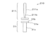
続いて、リフトピン30の形状や、リフトピン30の支持構造、リフトピン30を昇降するための構造について、図1を参照し、図2〜図5を用いて説明する。図2は、リフトピン30の構成の概略を示す説明図である。図3〜図5は、図1の成膜装置1の内部の状態を示す部分拡大断面図であり、図3は、載置台20が処理位置に移動されたときの状態を示し、図4は、載置台20が搬送位置に移動されたときの状態を示し、図5は、リフトピン30とウェハ搬送装置との間でウェハWが受け渡されるときの状態を示している。
Subsequently, the shape of the
リフトピン30は、図1〜図3に示すように、載置台20の下面より下側に位置する鍔部31aを含む第1部材31と、第1部材31とは別体であると共に載置台20の貫通孔20aに挿通される挿通部32aを含む第2部材32とを有する。第1部材31及び第2部材32は、例えばアルミナから形成される。
As shown in FIGS. 1 to 3, the
第1部材31は、上記鍔部31aが例えば上端に設けられている。この鍔部31aにより第1部材31が後述のピン支持部材100に係止される。また、第1部材31は、第2部材32が載置され当該第2部材を摺動自在に支持する摺動面31bを有する。言い換えると、第1部材31は、第2部材32が摺動面31bに沿って摺動自在となるように、第2部材32を下方から摺動面31bにより支持する。本例では、鍔部31aの上端面を含む第1部材31の上端面が上記摺動面31bとなる。また、第1部材31は、鍔部31aより下側の挿入部31cが棒状に形成されており、当該挿入部31cが図3に示すように後述のピン支持部材100の挿入孔101に挿入される。なお、上記挿入部31cは、第2部材32の挿通部32aに比べて、太く形成されている。
The
第2部材32は、図2に示すように、座部32bが、挿通部32aの下方、具体的には第2部材32の下端に設けられている。座部32bは、挿通部32aより大径であり且つ第1部材31の摺動面31bと当接する当接面32cを有する。
また、第2部材32の長さ(具体的には、第2部材32における、上端面から第1部材31の摺動面31bに対する当接面までの長さ)は、第1部材31から最も離間した位置すなわち処理位置の載置台20の下面から当該第1部材31の摺動面31bまでの距離より大きく設定されている。
As shown in FIG. 2, the
Further, the length of the second member 32 (specifically, the length from the upper end surface of the
上述のようなリフトピン30が下方から挿通される載置台20の貫通孔20aは、リフトピン30の第1部材31の鍔部31aより細く形成されている。言い換えると、載置台20の貫通孔20aの内径は、鍔部31aの直径より小さく設定されている。具体的には、例えば、リフトピン30の第2部材32の挿通部32aの直径は1.0mm〜3.0mmであり、鍔部31aの直径はその2倍以上であるのに対し、載置台20の貫通孔20aの内径はその1.2〜1.5倍に設定され、例えば、2.0〜4.0mmである。
The through
また、リフトピン30に対し、当該リフトピン30を支持可能に構成された部材であるピン支持部材100と、当該リフトピン30を支持可能に構成されると共に支持した当該リフトピン30を上下方向に移動させるピン移動機構110と、が設けられている。図1に示すように、ピン支持部材100は、載置台20と処理容器10の底壁との間に設けられ、ピン移動機構110は、ピン支持部材100と処理容器10の底壁との間に設けられている。言い換えると、ピン支持部材100は、処理容器10内において、載置台20とピン移動機構110との間に設けられている。
Further, with respect to the
ピン支持部材100は、リフトピン30の第1部材31の鍔部31aとの係合により当該リフトピン30を支持する。具体的には、ピン支持部材100は、鍔部31aとの係合により第1部材31を鉛直方向すなわち上下方向に移動自在に下方から支持し、これによりリフトピン30全体を上下方向に移動自在に下方から支持可能に構成されている。
ピン支持部材100は、図3に示すように、リフトピン30の第1部材31の挿入部31cが挿入され当該挿入部31cの外径よりその内径が大きい挿入孔101が形成されている。そして、ピン支持部材100は、当該ピン支持部材100における挿入孔101の周囲の上面と当該挿入孔101に挿入された第1部材31の鍔部31aの下面とが当接することにより、当該第1部材31を吊持し、これによりリフトピン30全体を吊持することができるように構成されている。また、上述のような構成により、第1部材31の挿入部31cが挿入孔101に挿入された状態で、水平方向に延びるピン支持部材100の上面に沿って当該第1部材31が摺動し、これによりリフトピン30全体がピン支持部材100の上面に沿って摺動可能となっている。なお、リフトピン30の第1部材31は、挿入部31cと挿入孔101とで規定される範囲内で、ピン支持部材100の上面に沿って水平方向に移動可能である。
挿入孔101の内径は、第1部材31の挿入部31cの直径の例えば1.2〜1.5倍に設定されている。
The
As shown in FIG. 3, the
The inner diameter of the
また、ピン支持部材100は、載置台20に対して固定されている。具体的には、ピン支持部材100は、例えば載置台20に接続された支軸部材23に取り付けられている。したがって、ピン支持部材100は、駆動機構24によって、載置台20と一体的に上下方向に移動され、また、載置台20と一体的に回転される。
Further, the
図3のように載置台20が処理位置に移動されている状態において、ピン支持部材100とリフトピン30の第1部材31の鍔部31aとは係合している。なお、この状態において以下の条件(A)、(B)を満たすように、リフトピン30の第2部材32の挿通部32aの長さは設定されている。
(A)第2部材32の挿通部32aの上端面が載置台20の上面から突出しない(例えば第2部材32の上端面は載置台20の上端面から0.1mm〜0.3mm下方に位置する)。
(B)挿通部32aの上端面が載置台20の下面より上方に位置し、挿通部32aの少なくとも一部が載置台20の貫通孔20aに挿通されている。
In a state where the mounting table 20 is moved to the processing position as shown in FIG. 3, the
(A) The upper end surface of the
(B) The upper end surface of the
上述の、ピン支持部材100とリフトピン30の第1部材31の鍔部31aとの係合は、図4に示すように、載置台20が搬送位置に移動されるだけでは解除されない。載置台20が搬送位置に移動されている状態において、図5に示すように、ピン移動機構110によりリフトピン30が上昇したときに、上記係合は解除される。ただし、載置台20が搬送位置に移動され、それと共にリフトピン30が下降する過程において、リフトピン30の第1部材31の下面とピン移動機構110の上面とが当接しリフトピン30のさらなる下降が妨げられ、載置台20の搬送位置への移動が完了した状態のときには上記係合が解除されているようにしてもよい。
As shown in FIG. 4, the above-mentioned engagement between the
なお、ピン支持部材100は、例えば、アルミナや石英等の低熱伝導率材料を用いた、平面視円環状の板状部材から構成される。ピン支持部材100の材料として低熱伝導材料を用いることにより、例えば、ピン支持部材100が取り付けられた載置台20の熱が当該ピン支持部材100により奪われるのを抑制することができる。また、ピン支持部材100に鉄系材料等を用いる場合、成膜装置1で形成する膜への鉄の混入が生じることがあるが、ピン支持部材100にアルミナや石英を用いることにより上記混入を防ぐことができる。
The
ピン移動機構110は、リフトピン30の第1部材31を支持可能に構成される共に、支持した第1部材31を上下方向に移動させ、これによりリフトピン30全体を上下方向に移動させる。ピン移動機構110は、リフトピン30の第1部材31の下端部との係合により当該リフトピン30を支持する。具体的には、ピン移動機構110は、当接部材111を有し、ピン支持部材100の挿入孔101に挿入され当該ピン支持部材100の下面から露出したリフトピン30の第1部材31の下端面と上記当接部材111の上面とが当接することにより、当該リフトピン30を支持する。当接部材111は、例えば平面視円環状の部材から構成される。
The
当接部材111の下面側には支持柱112が設けられており、支持柱112は、処理容器10の底壁を貫通して、処理容器10の外側に設けられた駆動機構113に接続されている。駆動機構113は、支持柱112を昇降させるための駆動力を発生する。支持柱112が駆動機構113の駆動により上下に移動することに伴って、当接部材111が上下に移動し、これにより当該当接部材111に支持されたリフトピン30が載置台20と独立して上下に移動する。特に、支持柱112が駆動機構113の駆動により上方に移動することに伴って、リフトピン30が上方に移動し、図5に示すように、当該リフトピン30の第2部材32の上端部が、搬送位置に移動された載置台20の上面から突出する。
A
ここで、リフトピン30が載置台20の上面から最も突出したときのリフトピン30の上端面から載置台20の下面までの距離、すなわち、リフトピン30の第2部材32における載置台20の貫通孔20aを通りうる部分の長さをL0とする。第2部材32の挿通部32aの長さ(より具体的にはリフトピン30の上端面から座部32bの上面までの距離)L1は、上記長さL0の1.1倍から1・5倍に設定されている。
Here, the distance from the upper end surface of the
なお、上述の駆動機構113と処理容器10の底壁における支持柱112の貫通部との間には、支持柱112の外周部を囲むように、ベローズ114が設けられている。これによって、処理容器10の気密が保たれる。
A bellows 114 is provided between the
ここで、リフトピン30の取付方法の一例について説明する。
例えば、支軸部材23を含む載置台20を裏返しておき、その載置台20の貫通孔20aそれぞれに、第1部材31と第2部材32とが冶具(図示せず)で互いに固定されたリフトピン30が挿入される。そして、そのリフトピン30の第1部材31がピン支持部材100の挿入孔101に挿入され、その状態でピン支持部材100が支軸部材23に取り付けられる。そして、裏返しにされていた載置台20が戻され、処理容器10内に取り付けられる。その後、第1部材31と第2部材32とを固定していた上記冶具が取り外される。リフトピン30の取付は例えばこのようにして行われる。
Here, an example of how to attach the
For example, the mounting table 20 including the
続いて、成膜装置1を用いて行われるウェハ処理について説明する。
まず、ゲートバルブ12が開かれ、処理容器10に隣接する真空雰囲気の搬送室(図示せず)から、搬入出口11を介して、ウェハWを保持したウェハ搬送装置M(図5参照)が処理容器10内に挿入される。そして、ウェハWが、前述の待機位置に移動されている載置台20の上方に搬送される。次いで、ピン支持部材100に吊持されていたリフトピン30が、ピン移動機構110により上昇する。具体的には、第2部材32を支持した第1部材31がピン移動機構110により載置台20及びウェハ搬送装置Mに対して上昇する。これにより、上記吊持が解除される共に、当該リフトピン30が載置台20の上面から所定距離突出し、当該リフトピン30の上に、具体的には、第2部材32の上にウェハWが受け渡される。
Subsequently, the wafer processing performed by using the
First, the
上述のようにウェハWの受け渡しのためにリフトピン30が上昇する際に、載置台20の貫通孔20aの位置が、当該載置台20の熱膨張や熱収縮等により、ピン支持部材100の挿入孔101に対してずれている場合がある。
上述の貫通孔20aの位置ずれが小さければ、リフトピンを上下方向に移動自在に支持すること、すなわち、リフトピンをフロート支持することで、上述の貫通孔20aの位置ずれに合わせてリフトピンの位置もずれるため、上述の貫通孔20aの位置ずれの影響はない。
しかし、本実施形態と異なりリフトピンが一体物であると(リフトピン30が互いに別体である第1部材31と第2部材32とで構成されず、一体物となっている場合)、上述の貫通孔20aの位置ずれが大きい場合、以下のような問題がある。
すなわち、上述の貫通孔20aの位置ずれが大きい場合、図6に示すようにリフトピン500が一体物であると、当該リフトピン500が傾くことがある。したがって、リフトピン500を上昇させたときに、当該リフトピン500が載置台20の下面等に当接することがある。また、当接後、リフトピン500の上昇が維持されると、リフトピン500における載置台20の貫通孔20aへの挿通部501の根元Bに大きな応力が生じ、リフトピン500が折れることがある。それに対し、本実施形態では、リフトピン30が、互いに別体である第1部材31と第2部材32とを有し、リフトピン30の第2部材32が第1部材31の摺動面31bに沿って摺動することができる。そのため、上述の貫通孔20aの位置ずれが大きい場合でも、図7に示すように、第2部材32は傾かず、または第2部材32の傾きは小さい。したがって、上述の貫通孔20aの位置ずれが大きい場合において、リフトピン30を上昇させても、第2部材32の挿通部32a等、当該リフトピン30には大きな応力が生じない。よって、リフトピン30の折れを防ぐことができる。
As described above, when the
If the misalignment of the through
However, unlike the present embodiment, if the lift pin is an integral body (when the
That is, when the above-mentioned through
リフトピン30上へのウェハWの受け渡し後、ウェハ搬送装置Mが処理容器10から抜き出され、ゲートバルブ12が閉じられる。それと共に、ピン移動機構110によるリフトピン30の下降、駆動機構24による載置台20の上昇が行われる。ピン移動機構110によるリフトピン30の下降では、具体的には、ウェハWが受け渡された第2部材32を支持した第1部材31が、ピン移動機構110により、載置台20に対して下降する。
上述のリフトピン30の下降、載置台20の上昇により、ピン移動機構110によるリフトピン30の支持が解除されリフトピン30が再びピン支持部材100により吊持される。それと共に、リフトピン30の上端部が載置台20の貫通孔20aに収納され上面から突出していない状態となり、リフトピン30の第2部材32から載置台20上へウェハWが受け渡される。次いで、処理容器10内が所定の圧力に調整され、駆動機構24により載置台20が処理位置へ移動され、処理空間Sが形成される。
After the wafer W is delivered onto the
When the
この状態で、ガス導入機構50を介して、処理空間Sに、パージガスであるN2ガスが供給されると共にTiCl4ガスとNH3ガスが交互に且つ間欠的に供給され、ALD法によりウェハW上にTiN膜が成膜される。この成膜の際、ウェハWは載置台20により加熱され、例えば、ウェハWの温度(具体的には載置台20の温度)は300℃〜600℃とされる。
In this state, N 2 gas, which is a purge gas, is supplied to the processing space S via the
上述のようなALD法でのTiN膜の成膜終了後、ウェハWが載置された載置台20が搬送位置まで下降される。次いで、ピン移動機構110によりリフトピン30が上昇する。具体的には、第2部材32を支持した第1部材31がピン移動機構110により載置台20及びウェハ搬送装置Mに対して上昇する。これにより、上記吊持が解除される共に、当該リフトピン30が載置台20の上面から所定距離突出し、当該リフトピン30の上に、具体的には、第2部材32の上にウェハWが受け渡される。その後、ゲートバルブ12が開かれ、搬入出口11を介して、ウェハWを保持していないウェハ搬送装置Mが処理容器10内に挿入される。ウェハ搬送装置Mは、リフトピン30に保持されたウェハWと搬送位置の載置台20との間まで挿入される。次いで、ピン移動機構110によりリフトピン30が下降する。具体的には、ウェハWが受け渡された第2部材32を支持した第1部材31が、ピン移動機構110により、ウェハ搬送装置Mに対して下降する。これにより、リフトピン30の第2部材32上のウェハWがウェハ搬送装置Mに受け渡される。そして、ウェハ搬送装置Mが処理容器10から抜き出され、ゲートバルブ12が閉じられる。これにより、一連のウェハ処理が完了する。
その後、他のウェハWに対し、上述の一連のウェハ処理が行われる。
After the formation of the TiN film by the ALD method as described above is completed, the mounting table 20 on which the wafer W is mounted is lowered to the transport position. Next, the
After that, the above-mentioned series of wafer processing is performed on the other wafer W.
以上のように、本実施形態では、載置台20に載置されたウェハWを当該載置台20で加熱する成膜装置1において、リフトピン30の載置台20の下面より下側に鍔部31aが設けられ、ピン支持部材100が、リフトピン30の鍔部31aとの係合により当該リフトピン30を支持している。つまりは、リフトピン30がピン支持部材100等に固定されていない。そのため、載置台20の熱膨張等の影響で、リフトピン30の破損や、リフトピン30の円滑な昇降動作が損なわれる可能性が低い。そして、本実施形態では、リフトピン30が挿通される載置台20の貫通孔20a(特にその上端部)が、リフトピン30の鍔部31aより細く形成され、従来のリフトピンよりも細径のリフトピンとすることができる。したがって、本実施形態によれば、例えば特許文献1のような形態に比べて、ウェハWの貫通孔20aに対応する部分の温度が低下するのを抑制することができるため、ウェハWの温度の面内均一性を改善することができる。さらに、本実施形態では、リフトピン30が、鍔部31aを含む第1部材31と、第1部材31とは別体であると共に挿通部32aを含む第2部材32とを有し、第1部材31が、第2部材32が載置され当該第2部材32を摺動自在に支持する摺動面31bを有する。したがって、載置台20の熱膨張等の影響で、リフトピン30の破損や、リフトピン30の円滑な昇降動作が損なわれる可能性をさらに低減することができる。特に、リフトピン30の折れを防止することができる。
なお、ウェハWの温度の面内均一性を改善する技術として、ウェハWのエッジを支持するエッジピンを用いる技術がある。しかし、この技術では、載置台にエッジピンが挿通される貫通孔を設ける必要があり、この挿通孔上にウェハWのエッジが位置するため、ウェハ裏面にも成膜されてしまう。本実施形態では、このようなウェハ裏面への成膜も生じない。
As described above, in the present embodiment, in the
As a technique for improving the in-plane uniformity of the temperature of the wafer W, there is a technique using an edge pin that supports the edge of the wafer W. However, in this technique, it is necessary to provide a through hole through which the edge pin is inserted in the mounting table, and since the edge of the wafer W is located on the insertion hole, a film is formed on the back surface of the wafer. In the present embodiment, such a film formation on the back surface of the wafer does not occur.
また、本実施形態では、リフトピン30を支持するために、異物の放出源と成り得るクランプ等の動作部材を用いていない。そのため、本実施形態によれば、ウェハW上に形成されたTiN膜の低品質化を防ぐことができる。
Further, in the present embodiment, in order to support the
さらに、本実施形態では、リフトピン30の第1部材31の挿入部31cが、第2部材32の挿通部32aに比べて、太く形成されている。したがって、リフトピン30をその下方からピン移動機構110で支持するときに、リフトピン30を安定的に支持することができる。
Further, in the present embodiment, the
さらにまた、本実施形態では、リフトピン30の第2部材32の挿通部32aの長さL1は、リフトピン30の第2部材32における載置台20の貫通孔20aを通りうる部分の長さL0の1.1倍から1・5倍に設定されている。つまり、本実施形態では、リフトピン30の挿通部32aの長さL1は、極力短く設定されている。そのため、リフトピン30の昇降時等に当該リフトピン30が載置台20に当接したとしても第2部材32に生じる応力が小さい。したがって、該応力による第2部材32の破損が生じにくいので、第2部材32の径を細くすることができ、載置台20の貫通孔20aの内径を細くすることができる。よって、ウェハWの温度の面内均一性をさらに改善することができる。
Furthermore, in the present embodiment, the length L1 of the
さらに、本実施形態では、上下方向に関し載置台20とピン移動機構110との間に設けられたピン支持部材100によりリフトピン30を支持するようにしている。したがって、ピン支持部材100を省略してピン移動機構110でリフトピン30を支持する構成に比べて、リフトピン30の第2部材32の長さを短くすることができる。したがって、上述と同様に、上記応力による第2部材32の破損が生じにくいので、第2部材32の径を細くすることができ、載置台20の貫通孔20aの内径を細くすることができる。よって、ウェハWの温度の面内均一性をさらに改善することができる。
Further, in the present embodiment, the
また、本実施形態では、第2部材32の長さが、第1部材31から最も離間した処理位置の載置台20の下面から当該第1部材31の摺動面31bまでの距離より大きい。言い換えると、第2部材32が、第1部材31に支持された状態において、挿通部32aの上端が成膜処理中に載置台20の貫通孔20a内に常に位置する長さを有する。そのため、成膜処理中に、第2部材32の上端が載置台20の貫通孔20aから抜けることがない。したがって、第2部材32が処理容器10内に落下するのを防止することができる。また、第2部材32と載置台20の貫通孔20aとの位置合わせが不要となる。
Further, in the present embodiment, the length of the
図8は、リフトピンの第2部材の他の例を説明する図である。
以上の例の第2部材32は座部32bが設けられていたが、図8のリフトピン200の第2部材201のように座部が設けられず全体として棒状に形成されていてもよい。ただし、図2のように座部32bを第2部材に設けることにより、第2部材を、より簡単に、傾いていない状態で支持することができる。
FIG. 8 is a diagram illustrating another example of the second member of the lift pin.
The
図9は、リフトピンの第2部材の他の例を説明する図である。図10は、載置台20の貫通孔20aに挿入された状態の図9のリフトピンの部分拡大断面図である。
図9のリフトピン210の第2部材211は、載置台20の貫通孔20aに挿通される挿通部211aに、細径部211bを有する。このように細径部211bに設けることにより、図10に示すように、第2部材211が傾いたとしても、そのまま上昇したときに、載置台20の貫通孔20aのエッジ20bに当たることがない。したがって、より確実に第2部材211の折れ、すなわちリフトピン210の折れを防止することができる。
FIG. 9 is a diagram illustrating another example of the second member of the lift pin. FIG. 10 is a partially enlarged cross-sectional view of the lift pin of FIG. 9 in a state of being inserted into the through
The
なお、細径部211bは、例えば、第2部材211において、当該第2部材211が最も上昇されたときの載置台20の貫通孔20aの下部に対応する位置に設けられる。図9の例では、挿通部211aの根元すなわち下端に設けられている。
また、細径部211bは、例えば下方に向かって小径になるテーパ形状を有する。この形状であれば、円筒状に比べて、第2部材211の強度を保ちながら当該第2部材211と載置台20の貫通孔20aのエッジ20bとの衝突を防ぐことができる。
The
Further, the
図11は、リフトピンの第2部材の他の例を説明する図である。
図11のリフトピン220のように第2部材221に鍔部が設けられていない場合においても、第2部材221に細径部211bを設けるようにしてもよい。
FIG. 11 is a diagram illustrating another example of the second member of the lift pin.
Even when the
図12は、リフトピンの第1部材の他の例を説明する部分断面図である。
図12のリフトピン230の第1部材231は、第2部材201の下側の部分が挿入される凹部231aを上側に有する。このように凹部231aを設けることにより、第2部材201の上端が載置台20の貫通孔20aから抜けたとしても、当該第2部材201が処理容器10内に落下するのを防ぐことができる。
なお、本例では、凹部231aの底面231bが第2部材201を摺動自在に支持する摺動面となる。
FIG. 12 is a partial cross-sectional view illustrating another example of the first member of the lift pin.
The
In this example, the
図13〜図15は、リフトピン30を吊持するピン支持部材の他の例を説明する図である。
図1の例のピン支持部材100は支軸部材23に取り付けられていたがリフトピン30を吊持する部材の取り付け位置はこの例に限られない。
13 to 15 are views for explaining another example of the pin support member for suspending the
The
図13の例のピン支持部材300は、載置台20に取り付けられている。このピン支持部材300は、小型化することができるため、当該ピン支持部材300の熱容量を小さくすることができる。したがって、ピン支持部材300により奪われる熱量を少なくすることができるため、ウェハWを効率的に加熱することができる。
The
図14の例のピン支持部材310は、被固定部材としてのフランジ25に取り付けられている。具体的には、ピン支持部材310は、上下方向に延在する脚部311を介して、フランジ25に取り付けられている。このピン支持部材310は、支軸部材23及び載置台20に取り付けられていないため、載置台20の熱が、直接または支軸部材23を介して、ピン支持部材310に奪われないため、ウェハWをより効率的に加熱することができる。
The
図15の例のピン支持部材320は、カバー部材330に取り付けられている。本例では、ピン支持部材320が、リフトピン30の第1部材31が挿入される挿入孔101が形成された平面視円環状の本体部321と、本体部321から外方に延びる複数の舌片部322とを有する。また、カバー部材330が、その上端から下方に延びるように形成されたL字状の爪部331を複数有する。ピン支持部材320の舌片部322とカバー部材330の爪部331との係合により、ピン支持部材320はカバー部材330に取り付けられる。
図14や図15の例のピン支持部材は、支軸部材23を含む載置台20の設計を変更せずに取り付けることができる。
The
The pin support members of the examples of FIGS. 14 and 15 can be attached without changing the design of the mounting
図16は、図1の例のピン支持部材100の変形例を示す平面図である。図1の例のピン支持部材100は、支軸部材23に取り付けられリフトピン30を支持するものであり、平面視円形の板状部材に主として支軸部材23の挿入孔及びリフトピン30の挿入孔101のみが設けたものである。しかし、支軸部材23に取り付けられるリフトピン30を支持する部材の形状はこの例に限られない。
FIG. 16 is a plan view showing a modified example of the
図16の例のピン支持部材340は、肉抜き部341を有する形状である。肉抜き部341は、リフトピン30と係合する領域以外の領域に形成されている。具体的には、肉抜き部341は、平面視において、リフトピン30が挿入される挿入孔101が形成された領域及び支軸部材23の挿入孔342が形成された領域以外の領域に形成されている。肉抜き部341は貫通孔であっても凹所であってもよい。
このピン支持部材340は、肉抜き部341を有するため、当該ピン支持部材340の熱容量を小さくすることができる。したがって、ピン支持部材340により奪われる熱量を少なくすることができるため、ウェハWを効率的に加熱することができる。
なお、肉抜き部は、図13〜図15の例のように、載置台20やフランジ25、カバー部材330に取り付けられるピン支持部材に設けてもよい。
The
Since the
The lightening portion may be provided on the mounting
以上の例では、リフトピン30を上下方向に移動させるピン移動機構110が設けられていたが、以下の条件(C)、(D)を満たす場合は、ピン移動機構110は省略しても良い。
(C)ウェハ搬送装置Mが上下方向に移動可能に構成されている。
(D)載置台20が搬送位置に移動されている状態においてリフトピン30の上端部が当該載置台20の上面から突出している。
In the above example, the
(C) The wafer transfer device M is configured to be movable in the vertical direction.
(D) The upper end of the
なお、この場合は、載置台20が搬送位置に移動される過程において、リフトピン30の下面と例えば処理容器10の底壁とが当接しリフトピン30のさらなる下方への移動が妨げられることで、載置台20が搬送位置に移動されている状態においてリフトピン30の上端部が当該載置台20の上面から突出する。
In this case, in the process of moving the mounting table 20 to the transport position, the lower surface of the
また、以上では、リフトピンの第1部材の載置面と当該載置面に対する第2部材の当接面とは共に平坦面であったが、いずれか一方または両方が曲面であってもよい。 Further, in the above, both the mounting surface of the first member of the lift pin and the contact surface of the second member with respect to the mounting surface are flat surfaces, but either one or both may be curved surfaces.
以上では、ALD法で成膜を行っていたが、本開示にかかる技術は、CVD法で成膜を行う場合にも適用することができる。例えば、Si含有ガスを使用してCVD法でSi膜やSiN膜を形成する場合にも、本開示にかかる技術を適用することができる。 In the above, the film formation was performed by the ALD method, but the technique according to the present disclosure can also be applied to the case where the film formation is performed by the CVD method. For example, the technique according to the present disclosure can be applied even when a Si film or a SiN film is formed by a CVD method using a Si-containing gas.
以上では、成膜装置を例に説明したが、本開示にかかる技術は、載置台を有する、成膜処理以外の処理を行う基板処理装置にも適用することができる。例えば、検査処理を行う検査装置やエッチング装置にも適用することができる。 In the above, the film forming apparatus has been described as an example, but the technique according to the present disclosure can also be applied to a substrate processing apparatus having a mounting table and performing a process other than the film forming process. For example, it can be applied to an inspection device or an etching device that performs an inspection process.
今回開示された実施形態はすべての点で例示であって制限的なものではないと考えられるべきである。上記の実施形態は、添付の請求の範囲及びその主旨を逸脱することなく、様々な形態で省略、置換、変更されてもよい。 It should be considered that the embodiments disclosed this time are exemplary in all respects and not restrictive. The above-described embodiment may be omitted, replaced, or changed in various forms without departing from the scope of the appended claims and the gist thereof.
なお、以下のような構成も本開示の技術的範囲に属する。
(1)基板を処理する基板処理装置であって、
上下方向に貫通する貫通孔を有し、上面に基板が載置されると共に載置された当該基板の加熱及び冷却の少なくともいずれか一方を行う載置台と、
前記貫通孔に挿通される挿通部が設けられ、当該挿通部が前記載置台の上面から前記貫通孔を介して突出可能に構成された基板支持ピンと、
前記基板支持ピンを支持可能に構成されたピン支持部材と、を備え、
前記基板支持ピンは、前記載置台の下面より下側に位置する鍔部が設けられ、
前記ピン支持部材は、前記鍔部との係合により前記基板支持ピンを支持し、
前記載置台の前記貫通孔は、前記基板支持ピンの前記鍔部より細く、
前記基板支持ピンは、前記鍔部を含む第1部材と、前記第1部材とは別体であり且つ前記挿通部を含む第2部材と、を有し、
前記第1部材は、前記第2部材が載置され当該第2部材を摺動自在に支持する摺動面を有する、基板処理装置。
前記(1)によれば、基板の温度の面内均一性を改善することができる。また、基板支持ピンの破損や、基板支持ピンの円滑な昇降動作が損なわれることを防止することができる。特に、基板支持ピンの折れを防止することができる。
The following configurations also belong to the technical scope of the present disclosure.
(1) A substrate processing device that processes a substrate.
A mounting table having a through hole penetrating in the vertical direction, in which a substrate is mounted on the upper surface and at least one of heating and cooling of the mounted substrate is performed.
A substrate support pin provided with an insertion portion to be inserted through the through hole, and the insertion portion can be projected from the upper surface of the above-mentioned pedestal through the through hole.
A pin support member configured to support the substrate support pin is provided.
The substrate support pin is provided with a flange portion located below the lower surface of the above-mentioned stand.
The pin support member supports the substrate support pin by engaging with the collar portion, and the pin support member supports the substrate support pin.
The through hole of the above-mentioned stand is thinner than the flange portion of the substrate support pin.
The substrate support pin has a first member including the collar portion and a second member that is separate from the first member and includes the insertion portion.
The first member is a substrate processing device having a sliding surface on which the second member is placed and slidably supports the second member.
According to the above (1), the in-plane uniformity of the temperature of the substrate can be improved. Further, it is possible to prevent the substrate support pin from being damaged and the smooth ascending / descending operation of the substrate support pin from being impaired. In particular, it is possible to prevent the substrate support pin from breaking.
(2)前記第2部材は、前記挿通部より大径であり且つ前記摺動面と当接する当接面を有する座部を含む、前記(1)に記載の基板処理装置。
前記(2)によれば、第2部材を、より簡単に、傾いていない状態で支持することができる。
(2) The substrate processing apparatus according to (1) above, wherein the second member includes a seat portion having a diameter larger than that of the insertion portion and having a contact surface that comes into contact with the sliding surface.
According to the above (2), the second member can be supported more easily in a non-tilted state.
(3)前記第2部材は、前記挿通部に細径部を有する、前記(1)または(2)に記載の基板処理装置。
前記(3)によれば、第2部材の折れをより確実に防止することができる。
(3) The substrate processing apparatus according to (1) or (2), wherein the second member has a small diameter portion in the insertion portion.
According to the above (3), it is possible to more reliably prevent the second member from breaking.
(4)前記第1部材は、前記第2部材の下側の部分が挿入される凹部を有する、前記(1)〜(3)のいずれか1に記載の基板処理装置。
前記(4)によれば、第2部材の上端が載置台の貫通孔から抜けたとしても、当該第2部材が処理容器内に落下するのを防ぐことができる。
(4) The substrate processing apparatus according to any one of (1) to (3) above, wherein the first member has a recess into which a lower portion of the second member is inserted.
According to the above (4), even if the upper end of the second member comes out of the through hole of the mounting table, it is possible to prevent the second member from falling into the processing container.
(5)前記第2部材の長さは、前記第1部材から最も離間した位置の前記載置台の下面から当該第1部材の前記摺動面までの距離より大きい、前記(1)〜(4)のいずれか1に記載の基板処理装置。
前記(5)によれば、基板処理中に、第2部材の上端が載置台の貫通孔から抜けることがない。
(5) The length of the second member is larger than the distance from the lower surface of the previously described pedestal at the position farthest from the first member to the sliding surface of the first member, the above (1) to (4). The substrate processing apparatus according to any one of).
According to the above (5), the upper end of the second member does not come out from the through hole of the mounting table during the substrate processing.
(6)前記基板支持ピンを上下方向に移動させるピン移動機構を備え、
前記ピン支持部材は、前記載置台と前記ピン移動機構との間に設けられている、前記(1)〜(5)のいずれか1に記載の基板処理装置。
前記(6)によれば、ピン支持部材を省略してピン移動機構で基板支持ピンを支持する構成に比べて、第2部材の長さを短くすることができる。そのため、基板支持ピンの昇降時等に当該基板支持ピンが貫通孔の内壁等に当接したときに当該基板支持ピンに生じる応力を小さくすることができる。したがって、基板支持ピンの径を細くすることができ、貫通孔の内径を細くすることができる。よって、基板の温度の面内均一性をさらに改善することができる。
(6) A pin moving mechanism for moving the board support pin in the vertical direction is provided.
The substrate processing device according to any one of (1) to (5) above, wherein the pin support member is provided between the above-mentioned stand and the pin moving mechanism.
According to the above (6), the length of the second member can be shortened as compared with the configuration in which the pin support member is omitted and the substrate support pin is supported by the pin moving mechanism. Therefore, it is possible to reduce the stress generated in the substrate support pin when the substrate support pin comes into contact with the inner wall of the through hole or the like when the substrate support pin is raised or lowered. Therefore, the diameter of the substrate support pin can be reduced, and the inner diameter of the through hole can be reduced. Therefore, the in-plane uniformity of the temperature of the substrate can be further improved.
(7)前記ピン支持部材は、前記第1部材の前記鍔部より下側の部分が挿入される挿入孔を有する、前記(1)〜(6)のいずれか1に記載の基板処理装置。
前記(7)によれば、ピン支持部材で第1部材を吊持することができる。
(7) The substrate processing apparatus according to any one of (1) to (6) above, wherein the pin support member has an insertion hole into which a portion of the first member below the collar portion is inserted.
According to (7) above, the first member can be suspended by the pin support member.
(8)前記載置台を上下方向に移動させる移動機構を備える、前記(1)〜(7)のいずれか1に記載の基板処理装置。 (8) The substrate processing apparatus according to any one of (1) to (7) above, further comprising a moving mechanism for moving the above-mentioned stand in the vertical direction.
(9)前記第2部材の前記挿通部の直径は1.0〜3.0mmであり、前記貫通孔の内径は2.0〜4.0mmである、前記(1)〜(8)のいずれか1に記載の基板処理装置。 (9) Any of the above (1) to (8), wherein the diameter of the insertion portion of the second member is 1.0 to 3.0 mm, and the inner diameter of the through hole is 2.0 to 4.0 mm. The substrate processing apparatus according to 1.
(10)前記載置台の下面に上端部が接続され前記載置台を支持する台支持部材を備え、
前記ピン支持部材は、前記台支持部材に取り付けられている、前記(1)〜(9)のいずれか1に記載の基板処理装置。
(10) A table support member having an upper end connected to the lower surface of the previously described table to support the previously described table is provided.
The substrate processing apparatus according to any one of (1) to (9) above, wherein the pin support member is attached to the base support member.
(11)前記ピン支持部材は、前記載置台の下面に取り付けられている、前記(1)〜(9)のいずれか1に記載の基板処理装置。 (11) The substrate processing apparatus according to any one of (1) to (9) above, wherein the pin support member is attached to the lower surface of the above-mentioned stand.
(12)前記載置台の下面に上端部が接続され前記載置台を支持する台支持部材と
前記台支持部材が固定される被固定部材と、を備え、
前記ピン支持部材は、前記被固定部材に取り付けられている、前記(1)〜(9)のいずれか1に記載の基板処理装置。
(12) A pedestal support member whose upper end is connected to the lower surface of the previously described pedestal to support the previously described pedestal and a fixed member to which the pedestal support member is fixed are provided.
The substrate processing apparatus according to any one of (1) to (9) above, wherein the pin support member is attached to the fixed member.
(13)前記載置台の側面を覆うカバー部材を備え、
前記ピン支持部材は、前記カバー部材に支持されている、前記(1)〜(9)のいずれか1に記載の基板処理装置。
(13) A cover member for covering the side surface of the above-mentioned stand is provided.
The substrate processing apparatus according to any one of (1) to (9) above, wherein the pin support member is supported by the cover member.
(14)前記ピン支持部材は、前記基板支持ピンの前記鍔部と係合する領域以外の領域に、肉抜き部を有する、前記(1)〜(13)のいずれか1に記載の基板処理装置。
前記(14)によれば、ピン支持部材の熱容量を小さくすることができる。したがって、基板を効率的に加熱または冷却することができる。
(14) The substrate treatment according to any one of (1) to (13) above, wherein the pin support member has a lightening portion in a region other than the region of the substrate support pin that engages with the collar portion. apparatus.
According to (14) above, the heat capacity of the pin support member can be reduced. Therefore, the substrate can be efficiently heated or cooled.
(15)基板処理装置における基板搬送装置との間での基板の受け渡し方法であって、
前記基板処理装置は、
上下方向に貫通する貫通孔を有し、上面に基板が載置されると共に載置された当該基板の加熱及び冷却の少なくともいずれか一方を行う載置台と、
前記貫通孔に挿通される挿通部が設けられ、当該挿通部が前記載置台の上面から前記貫通孔を介して突出可能に構成された基板支持ピンと、
前記基板支持ピンを支持可能に構成されたピン支持部材と、を備え、
前記基板支持ピンは、前記載置台の下面より下側に位置する鍔部が設けられ、
前記ピン支持部材は、前記鍔部との係合により前記基板支持ピンを支持し、
前記載置台の前記貫通孔は、前記基板支持ピンの前記鍔部より細く、
前記基板支持ピンは、前記鍔部を含む第1部材と、前記第1部材とは別体であり且つ前記挿通部を含む第2部材と、を有し、
前記第1部材は、前記第2部材が載置され当該第2部材を摺動自在に支持する摺動面を有し、
当該基板の受け渡し方法は、
前記第2部材を支持した前記第1部材を前記載置台または前記基板搬送装置に対して上昇させ、当該載置台または当該基板搬送装置の前記基板を当該第2部材に受け渡す工程と、
前記載置台から前記基板が受け渡された前記第2部材を支持した前記第1部材を前記基板搬送装置に対して下降させ当該第2部材から当該基板搬送装置上に前記基板を受け渡し、または、前記基板搬送装置から前記基板が受け渡された前記第2部材を支持した前記第1部材を前記載置台に対して下降させ当該第2部材から当該載置台上に前記基板を受け渡す工程と、を含む、基板の受け渡し方法。
(15) A method of delivering a substrate to and from a substrate transporting apparatus in a substrate processing apparatus.
The substrate processing device is
A mounting table having a through hole penetrating in the vertical direction, in which a substrate is mounted on the upper surface and at least one of heating and cooling of the mounted substrate is performed.
A substrate support pin provided with an insertion portion to be inserted through the through hole, and the insertion portion can be projected from the upper surface of the above-mentioned pedestal through the through hole.
A pin support member configured to support the substrate support pin is provided.
The substrate support pin is provided with a flange portion located below the lower surface of the above-mentioned stand.
The pin support member supports the substrate support pin by engaging with the collar portion, and the pin support member supports the substrate support pin.
The through hole of the above-mentioned stand is thinner than the flange portion of the substrate support pin.
The substrate support pin has a first member including the collar portion and a second member that is separate from the first member and includes the insertion portion.
The first member has a sliding surface on which the second member is placed and slidably supports the second member.
The method of delivering the board is
A step of raising the first member supporting the second member with respect to the above-mentioned stand or the substrate transfer device, and delivering the substrate of the mount or the substrate transfer device to the second member.
The first member supporting the second member to which the substrate has been delivered from the above-mentioned stand is lowered with respect to the substrate transfer device, and the substrate is delivered from the second member onto the substrate transfer device, or A step of lowering the first member supporting the second member to which the substrate has been delivered from the substrate transfer device with respect to the above-mentioned pedestal and delivering the substrate from the second member onto the pedestal. How to deliver the board, including.
1 成膜装置
20 載置台
20a 貫通孔
30、200、210、220、230 リフトピン
31、231 第1部材
31a 鍔部
31b 摺動面
32、201、211、221 第2部材
32a、211a 挿通部
100、300、310、320、340 ピン支持部材
M ウェハ搬送装置
W ウェハ
1
Claims (15)
上下方向に貫通する貫通孔を有し、上面に基板が載置されると共に載置された当該基板の加熱及び冷却の少なくともいずれか一方を行う載置台と、
前記貫通孔に挿通される挿通部が設けられ、当該挿通部が前記載置台の上面から前記貫通孔を介して突出可能に構成された基板支持ピンと、
前記基板支持ピンを支持可能に構成されたピン支持部材と、を備え、
前記基板支持ピンは、前記載置台の下面より下側に位置する鍔部が設けられ、
前記ピン支持部材は、前記鍔部との係合により前記基板支持ピンを支持し、
前記載置台の前記貫通孔は、前記基板支持ピンの前記鍔部より細く、
前記基板支持ピンは、前記鍔部を含む第1部材と、前記第1部材とは別体であり且つ前記挿通部を含む第2部材と、を有し、
前記第1部材は、前記第2部材が載置され当該第2部材を摺動自在に支持する摺動面を有する、基板処理装置。 A substrate processing device that processes substrates
A mounting table having a through hole penetrating in the vertical direction, in which a substrate is mounted on the upper surface and at least one of heating and cooling of the mounted substrate is performed.
A substrate support pin provided with an insertion portion to be inserted through the through hole, and the insertion portion can be projected from the upper surface of the above-mentioned pedestal through the through hole.
A pin support member configured to support the substrate support pin is provided.
The substrate support pin is provided with a flange portion located below the lower surface of the above-mentioned stand.
The pin support member supports the substrate support pin by engaging with the collar portion, and the pin support member supports the substrate support pin.
The through hole of the above-mentioned stand is thinner than the flange portion of the substrate support pin.
The substrate support pin has a first member including the collar portion and a second member that is separate from the first member and includes the insertion portion.
The first member is a substrate processing device having a sliding surface on which the second member is placed and slidably supports the second member.
前記ピン支持部材は、前記載置台と前記ピン移動機構との間に設けられている、請求項1〜5のいずれか1項に記載の基板処理装置。 A pin moving mechanism for moving the board support pin in the vertical direction is provided.
The substrate processing device according to any one of claims 1 to 5, wherein the pin support member is provided between the above-mentioned stand and the pin moving mechanism.
前記ピン支持部材は、前記台支持部材に取り付けられている、請求項1〜9のいずれか1項に記載の基板処理装置。 A stand support member whose upper end is connected to the lower surface of the above-mentioned stand to support the above-mentioned stand is provided.
The substrate processing apparatus according to any one of claims 1 to 9, wherein the pin support member is attached to the base support member.
前記台支持部材が固定される被固定部材と、を備え、
前記ピン支持部材は、前記被固定部材に取り付けられている、請求項1〜9のいずれか1項に記載の基板処理装置。 A stand support member whose upper end is connected to the lower surface of the above-mentioned stand to support the above-mentioned stand and a fixed member to which the stand support member is fixed are provided.
The substrate processing apparatus according to any one of claims 1 to 9, wherein the pin support member is attached to the fixed member.
前記ピン支持部材は、前記カバー部材に支持されている、請求項1〜9のいずれか1項に記載の基板処理装置。 Equipped with a cover member that covers the side surface of the above-mentioned stand
The substrate processing apparatus according to any one of claims 1 to 9, wherein the pin support member is supported by the cover member.
前記基板処理装置は、
上下方向に貫通する貫通孔を有し、上面に基板が載置されると共に載置された当該基板の加熱及び冷却の少なくともいずれか一方を行う載置台と、
前記貫通孔に挿通される挿通部が設けられ、当該挿通部が前記載置台の上面から前記貫通孔を介して突出可能に構成された基板支持ピンと、
前記基板支持ピンを支持可能に構成されたピン支持部材と、を備え、
前記基板支持ピンは、前記載置台の下面より下側に位置する鍔部が設けられ、
前記ピン支持部材は、前記鍔部との係合により前記基板支持ピンを支持し、
前記載置台の前記貫通孔は、前記基板支持ピンの前記鍔部より細く、
前記基板支持ピンは、前記鍔部を含む第1部材と、前記第1部材とは別体であり且つ前記挿通部を含む第2部材と、を有し、
前記第1部材は、前記第2部材が載置され当該第2部材を摺動自在に支持する摺動面を有し、
当該基板の受け渡し方法は、
前記第2部材を支持した前記第1部材を前記載置台または前記基板搬送装置に対して上昇させ、当該載置台または当該基板搬送装置の前記基板を当該第2部材に受け渡す工程と、
前記載置台から前記基板が受け渡された前記第2部材を支持した前記第1部材を前記基板搬送装置に対して下降させ当該第2部材から当該基板搬送装置上に前記基板を受け渡し、または、前記基板搬送装置から前記基板が受け渡された前記第2部材を支持した前記第1部材を前記載置台に対して下降させ当該第2部材から当該載置台上に前記基板を受け渡す工程と、を含む、基板の受け渡し方法。 It is a method of transferring a substrate to and from a substrate transporting apparatus in a substrate processing apparatus.
The substrate processing device is
A mounting table having a through hole penetrating in the vertical direction, in which a substrate is mounted on the upper surface and at least one of heating and cooling of the mounted substrate is performed.
A substrate support pin provided with an insertion portion to be inserted through the through hole, and the insertion portion can be projected from the upper surface of the above-mentioned pedestal through the through hole.
A pin support member configured to support the substrate support pin is provided.
The substrate support pin is provided with a flange portion located below the lower surface of the above-mentioned stand.
The pin support member supports the substrate support pin by engaging with the collar portion, and the pin support member supports the substrate support pin.
The through hole of the above-mentioned stand is thinner than the flange portion of the substrate support pin.
The substrate support pin has a first member including the collar portion and a second member that is separate from the first member and includes the insertion portion.
The first member has a sliding surface on which the second member is placed and slidably supports the second member.
The method of delivering the board is
A step of raising the first member supporting the second member with respect to the above-mentioned stand or the substrate transfer device, and delivering the substrate of the mount or the substrate transfer device to the second member.
The first member supporting the second member to which the substrate has been delivered from the above-mentioned stand is lowered with respect to the substrate transfer device, and the substrate is delivered from the second member onto the substrate transfer device, or A step of lowering the first member supporting the second member to which the substrate has been delivered from the substrate transfer device with respect to the above-mentioned pedestal and delivering the substrate from the second member onto the pedestal. How to deliver the board, including.
Priority Applications (4)
| Application Number | Priority Date | Filing Date | Title |
|---|---|---|---|
| JP2019126198A JP2021012944A (en) | 2019-07-05 | 2019-07-05 | Substrate processing apparatus and substrate delivery method |
| KR1020200077637A KR102437343B1 (en) | 2019-07-05 | 2020-06-25 | Substrate processing apparatus and substrate delivery method |
| CN202010600872.7A CN112185882B (en) | 2019-07-05 | 2020-06-28 | Substrate processing apparatus and substrate transfer method |
| US16/915,046 US11664266B2 (en) | 2019-07-05 | 2020-06-29 | Substrate processing apparatus and substrate delivery method |
Applications Claiming Priority (1)
| Application Number | Priority Date | Filing Date | Title |
|---|---|---|---|
| JP2019126198A JP2021012944A (en) | 2019-07-05 | 2019-07-05 | Substrate processing apparatus and substrate delivery method |
Publications (1)
| Publication Number | Publication Date |
|---|---|
| JP2021012944A true JP2021012944A (en) | 2021-02-04 |
Family
ID=73919120
Family Applications (1)
| Application Number | Title | Priority Date | Filing Date |
|---|---|---|---|
| JP2019126198A Withdrawn JP2021012944A (en) | 2019-07-05 | 2019-07-05 | Substrate processing apparatus and substrate delivery method |
Country Status (4)
| Country | Link |
|---|---|
| US (1) | US11664266B2 (en) |
| JP (1) | JP2021012944A (en) |
| KR (1) | KR102437343B1 (en) |
| CN (1) | CN112185882B (en) |
Cited By (2)
| Publication number | Priority date | Publication date | Assignee | Title |
|---|---|---|---|---|
| JP2022148699A (en) * | 2021-03-24 | 2022-10-06 | 東京エレクトロン株式会社 | Plasma processing system and method for fitting annular member |
| JP2023000780A (en) * | 2021-06-18 | 2023-01-04 | 東京エレクトロン株式会社 | Plasma processing apparatus |
Families Citing this family (8)
| Publication number | Priority date | Publication date | Assignee | Title |
|---|---|---|---|---|
| JP2020177967A (en) * | 2019-04-16 | 2020-10-29 | 東京エレクトロン株式会社 | Board processing equipment |
| JP7394554B2 (en) * | 2019-08-07 | 2023-12-08 | 東京エレクトロン株式会社 | Substrate processing system |
| CN115142045B (en) * | 2021-03-29 | 2023-12-19 | 鑫天虹(厦门)科技有限公司 | Bearing disc capable of accurately adjusting temperature and thin film deposition device |
| FI130021B (en) | 2021-05-10 | 2022-12-30 | Picosun Oy | Substrate processing apparatus and method |
| JP7708512B2 (en) * | 2021-07-28 | 2025-07-15 | 東京エレクトロン株式会社 | Substrate Processing Equipment |
| JP7715464B2 (en) * | 2021-09-02 | 2025-07-30 | 東京エレクトロン株式会社 | Substrate Processing Equipment |
| KR102835218B1 (en) | 2022-04-12 | 2025-07-18 | 삼성디스플레이 주식회사 | Exposure device and method of manufacturing display device using the same |
| JP7845787B2 (en) * | 2022-05-06 | 2026-04-14 | 東京エレクトロン株式会社 | Substrate processing apparatus and method for manufacturing a substrate processing apparatus |
Family Cites Families (23)
| Publication number | Priority date | Publication date | Assignee | Title |
|---|---|---|---|---|
| JPH11111821A (en) | 1997-10-03 | 1999-04-23 | Kokusai Electric Co Ltd | Substrate support device |
| JP3602324B2 (en) * | 1998-02-17 | 2004-12-15 | アルプス電気株式会社 | Plasma processing equipment |
| JP3398936B2 (en) * | 1999-04-09 | 2003-04-21 | 日本エー・エス・エム株式会社 | Semiconductor processing equipment |
| DE10003639C2 (en) * | 2000-01-28 | 2003-06-18 | Steag Rtp Systems Gmbh | Device for the thermal treatment of substrates |
| JP4203206B2 (en) * | 2000-03-24 | 2008-12-24 | 株式会社日立国際電気 | Substrate processing equipment |
| JP2003100855A (en) * | 2001-09-27 | 2003-04-04 | Shin Etsu Handotai Co Ltd | Silicon single crystal wafer processing apparatus, silicon single crystal wafer, and method for manufacturing silicon epitaxial wafer |
| US20030178145A1 (en) * | 2002-03-25 | 2003-09-25 | Applied Materials, Inc. | Closed hole edge lift pin and susceptor for wafer process chambers |
| KR20030091301A (en) * | 2002-05-27 | 2003-12-03 | 삼성전자주식회사 | wafer lifter of semiconductor device manufacturing equipment |
| JP4363401B2 (en) * | 2003-03-26 | 2009-11-11 | 信越半導体株式会社 | Heat treatment wafer support and heat treatment apparatus |
| JP4628964B2 (en) * | 2005-04-26 | 2011-02-09 | 大日本スクリーン製造株式会社 | Substrate processing equipment |
| CN100477147C (en) * | 2006-03-16 | 2009-04-08 | 东京毅力科创株式会社 | Substrate table and substrate processing apparatus |
| JP4795899B2 (en) * | 2006-08-31 | 2011-10-19 | 東京エレクトロン株式会社 | Substrate mounting mechanism and substrate delivery method |
| JP4799325B2 (en) * | 2006-09-05 | 2011-10-26 | 東京エレクトロン株式会社 | Substrate delivery apparatus, substrate processing apparatus, and substrate delivery method |
| KR100854500B1 (en) * | 2007-02-12 | 2008-08-26 | 삼성전자주식회사 | Chuck Assembly and High Density Plasma Equipment |
| JP5262878B2 (en) * | 2009-03-17 | 2013-08-14 | 東京エレクトロン株式会社 | Mounting table structure and plasma deposition apparatus |
| WO2012046397A1 (en) * | 2010-10-07 | 2012-04-12 | キヤノンアネルバ株式会社 | Substrate processing device |
| JP5214774B2 (en) * | 2010-11-19 | 2013-06-19 | 株式会社日立国際電気 | Substrate processing apparatus and semiconductor device manufacturing method |
| US20130025538A1 (en) * | 2011-07-27 | 2013-01-31 | Applied Materials, Inc. | Methods and apparatus for deposition processes |
| TWI624903B (en) * | 2013-03-15 | 2018-05-21 | 應用材料股份有限公司 | On-site temperature measurement in a noise environment |
| JP6494536B2 (en) * | 2016-01-12 | 2019-04-03 | 東京エレクトロン株式会社 | Substrate processing apparatus and substrate processing apparatus cleaning method |
| JP6685216B2 (en) * | 2016-01-26 | 2020-04-22 | 東京エレクトロン株式会社 | Film forming apparatus, film forming method, program, and computer-readable storage medium |
| WO2017169032A1 (en) * | 2016-03-28 | 2017-10-05 | 株式会社日立国際電気 | Substrate-processing device, temperature-measuring unit, and method for manufacturing semiconductor device |
| DE102016212780A1 (en) * | 2016-07-13 | 2018-01-18 | Siltronic Ag | Device for handling a semiconductor wafer in an epitaxial reactor and method for producing a semiconductor wafer with an epitaxial layer |
-
2019
- 2019-07-05 JP JP2019126198A patent/JP2021012944A/en not_active Withdrawn
-
2020
- 2020-06-25 KR KR1020200077637A patent/KR102437343B1/en active Active
- 2020-06-28 CN CN202010600872.7A patent/CN112185882B/en active Active
- 2020-06-29 US US16/915,046 patent/US11664266B2/en active Active
Cited By (6)
| Publication number | Priority date | Publication date | Assignee | Title |
|---|---|---|---|---|
| JP2022148699A (en) * | 2021-03-24 | 2022-10-06 | 東京エレクトロン株式会社 | Plasma processing system and method for fitting annular member |
| JP7534249B2 (en) | 2021-03-24 | 2024-08-14 | 東京エレクトロン株式会社 | Plasma processing system and method for mounting an annular member - Patents.com |
| JP2024153861A (en) * | 2021-03-24 | 2024-10-29 | 東京エレクトロン株式会社 | Plasma processing system and method for mounting an annular member - Patents.com |
| JP7763302B2 (en) | 2021-03-24 | 2025-10-31 | 東京エレクトロン株式会社 | Plasma processing system and method for mounting an annular member |
| JP2023000780A (en) * | 2021-06-18 | 2023-01-04 | 東京エレクトロン株式会社 | Plasma processing apparatus |
| JP7617816B2 (en) | 2021-06-18 | 2025-01-20 | 東京エレクトロン株式会社 | Plasma Processing Equipment |
Also Published As
| Publication number | Publication date |
|---|---|
| CN112185882B (en) | 2024-05-03 |
| US11664266B2 (en) | 2023-05-30 |
| KR102437343B1 (en) | 2022-08-30 |
| KR20210004847A (en) | 2021-01-13 |
| US20210005505A1 (en) | 2021-01-07 |
| CN112185882A (en) | 2021-01-05 |
Similar Documents
| Publication | Publication Date | Title |
|---|---|---|
| JP2021012944A (en) | Substrate processing apparatus and substrate delivery method | |
| KR102398454B1 (en) | Substrate processing apparatus | |
| KR102097109B1 (en) | Deposition apparatus | |
| JP2021097162A (en) | Substrate processing device and mounting table | |
| US20210005502A1 (en) | Stage, substrate processing apparatus and stage assembling method | |
| US11104991B2 (en) | Processing apparatus and cover member | |
| CN101097844B (en) | Semiconductor processing equipment | |
| TWI442510B (en) | Base unit and device for processing the substrate using the base unit | |
| TW201621977A (en) | Device and wafer processing method and device for changing gas flow mode | |
| TW201708601A (en) | Processing kit with flow isolation ring | |
| KR20110112074A (en) | Substrate Processing Apparatus and Method | |
| US20250354259A1 (en) | Film formation apparatus, film formation method, and substrate support member | |
| KR101139692B1 (en) | Chemical vapor deposition device | |
| TW201528415A (en) | Lift pin assembly and substrate processing device having lift pin assembly | |
| KR20190063286A (en) | Movement method of Lift pin and Substrate process apparatus | |
| US12297536B2 (en) | Substrate processing apparatus and substrate processing method | |
| KR20100045072A (en) | Apparatus for treatment of plural substrates | |
| JP2020193379A (en) | Stage structure, substrate processing device and method of controlling stage structure | |
| JP2021068871A (en) | Epitaxial growth device and method of manufacturing epitaxial wafer | |
| KR101771901B1 (en) | Substrate processing apparatus | |
| TW202419681A (en) | Single piece or two piece susceptor | |
| JP2004186552A (en) | Substrate processing equipment | |
| JP2022083011A (en) | Susceptor and cvd equipment | |
| KR20080051838A (en) | Particle removal apparatus and method using N2 purge nozzle of epitaxial equipment |
Legal Events
| Date | Code | Title | Description |
|---|---|---|---|
| A621 | Written request for application examination |
Free format text: JAPANESE INTERMEDIATE CODE: A621 Effective date: 20220316 |
|
| A761 | Written withdrawal of application |
Free format text: JAPANESE INTERMEDIATE CODE: A761 Effective date: 20221227 |