JP2019105623A - Transmission/reception module for optoelectronic sensor, and method of detecting objects - Google Patents
Transmission/reception module for optoelectronic sensor, and method of detecting objects Download PDFInfo
- Publication number
- JP2019105623A JP2019105623A JP2018197512A JP2018197512A JP2019105623A JP 2019105623 A JP2019105623 A JP 2019105623A JP 2018197512 A JP2018197512 A JP 2018197512A JP 2018197512 A JP2018197512 A JP 2018197512A JP 2019105623 A JP2019105623 A JP 2019105623A
- Authority
- JP
- Japan
- Prior art keywords
- light
- receiver
- emitter
- optical system
- receiving
- Prior art date
- Legal status (The legal status is an assumption and is not a legal conclusion. Google has not performed a legal analysis and makes no representation as to the accuracy of the status listed.)
- Granted
Links
Images


Classifications
-
- G—PHYSICS
- G01—MEASURING; TESTING
- G01S—RADIO DIRECTION-FINDING; RADIO NAVIGATION; DETERMINING DISTANCE OR VELOCITY BY USE OF RADIO WAVES; LOCATING OR PRESENCE-DETECTING BY USE OF THE REFLECTION OR RERADIATION OF RADIO WAVES; ANALOGOUS ARRANGEMENTS USING OTHER WAVES
- G01S17/00—Systems using the reflection or reradiation of electromagnetic waves other than radio waves, e.g. lidar systems
- G01S17/02—Systems using the reflection of electromagnetic waves other than radio waves
- G01S17/06—Systems determining position data of a target
- G01S17/08—Systems determining position data of a target for measuring distance only
-
- G—PHYSICS
- G01—MEASURING; TESTING
- G01S—RADIO DIRECTION-FINDING; RADIO NAVIGATION; DETERMINING DISTANCE OR VELOCITY BY USE OF RADIO WAVES; LOCATING OR PRESENCE-DETECTING BY USE OF THE REFLECTION OR RERADIATION OF RADIO WAVES; ANALOGOUS ARRANGEMENTS USING OTHER WAVES
- G01S17/00—Systems using the reflection or reradiation of electromagnetic waves other than radio waves, e.g. lidar systems
- G01S17/02—Systems using the reflection of electromagnetic waves other than radio waves
- G01S17/06—Systems determining position data of a target
- G01S17/42—Simultaneous measurement of distance and other co-ordinates
-
- G—PHYSICS
- G01—MEASURING; TESTING
- G01C—MEASURING DISTANCES, LEVELS OR BEARINGS; SURVEYING; NAVIGATION; GYROSCOPIC INSTRUMENTS; PHOTOGRAMMETRY OR VIDEOGRAMMETRY
- G01C3/00—Measuring distances in line of sight; Optical rangefinders
- G01C3/02—Details
- G01C3/06—Use of electric means to obtain final indication
- G01C3/08—Use of electric radiation detectors
-
- G—PHYSICS
- G01—MEASURING; TESTING
- G01S—RADIO DIRECTION-FINDING; RADIO NAVIGATION; DETERMINING DISTANCE OR VELOCITY BY USE OF RADIO WAVES; LOCATING OR PRESENCE-DETECTING BY USE OF THE REFLECTION OR RERADIATION OF RADIO WAVES; ANALOGOUS ARRANGEMENTS USING OTHER WAVES
- G01S17/00—Systems using the reflection or reradiation of electromagnetic waves other than radio waves, e.g. lidar systems
- G01S17/02—Systems using the reflection of electromagnetic waves other than radio waves
- G01S17/06—Systems determining position data of a target
- G01S17/08—Systems determining position data of a target for measuring distance only
- G01S17/10—Systems determining position data of a target for measuring distance only using transmission of interrupted, pulse-modulated waves
-
- G—PHYSICS
- G01—MEASURING; TESTING
- G01S—RADIO DIRECTION-FINDING; RADIO NAVIGATION; DETERMINING DISTANCE OR VELOCITY BY USE OF RADIO WAVES; LOCATING OR PRESENCE-DETECTING BY USE OF THE REFLECTION OR RERADIATION OF RADIO WAVES; ANALOGOUS ARRANGEMENTS USING OTHER WAVES
- G01S7/00—Details of systems according to groups G01S13/00, G01S15/00, G01S17/00
- G01S7/48—Details of systems according to groups G01S13/00, G01S15/00, G01S17/00 of systems according to group G01S17/00
- G01S7/4808—Evaluating distance, position or velocity data
-
- G—PHYSICS
- G01—MEASURING; TESTING
- G01S—RADIO DIRECTION-FINDING; RADIO NAVIGATION; DETERMINING DISTANCE OR VELOCITY BY USE OF RADIO WAVES; LOCATING OR PRESENCE-DETECTING BY USE OF THE REFLECTION OR RERADIATION OF RADIO WAVES; ANALOGOUS ARRANGEMENTS USING OTHER WAVES
- G01S7/00—Details of systems according to groups G01S13/00, G01S15/00, G01S17/00
- G01S7/48—Details of systems according to groups G01S13/00, G01S15/00, G01S17/00 of systems according to group G01S17/00
- G01S7/481—Constructional features, e.g. arrangements of optical elements
-
- G—PHYSICS
- G01—MEASURING; TESTING
- G01S—RADIO DIRECTION-FINDING; RADIO NAVIGATION; DETERMINING DISTANCE OR VELOCITY BY USE OF RADIO WAVES; LOCATING OR PRESENCE-DETECTING BY USE OF THE REFLECTION OR RERADIATION OF RADIO WAVES; ANALOGOUS ARRANGEMENTS USING OTHER WAVES
- G01S7/00—Details of systems according to groups G01S13/00, G01S15/00, G01S17/00
- G01S7/48—Details of systems according to groups G01S13/00, G01S15/00, G01S17/00 of systems according to group G01S17/00
- G01S7/481—Constructional features, e.g. arrangements of optical elements
- G01S7/4811—Constructional features, e.g. arrangements of optical elements common to transmitter and receiver
- G01S7/4812—Constructional features, e.g. arrangements of optical elements common to transmitter and receiver transmitted and received beams following a coaxial path
-
- G—PHYSICS
- G01—MEASURING; TESTING
- G01S—RADIO DIRECTION-FINDING; RADIO NAVIGATION; DETERMINING DISTANCE OR VELOCITY BY USE OF RADIO WAVES; LOCATING OR PRESENCE-DETECTING BY USE OF THE REFLECTION OR RERADIATION OF RADIO WAVES; ANALOGOUS ARRANGEMENTS USING OTHER WAVES
- G01S7/00—Details of systems according to groups G01S13/00, G01S15/00, G01S17/00
- G01S7/48—Details of systems according to groups G01S13/00, G01S15/00, G01S17/00 of systems according to group G01S17/00
- G01S7/481—Constructional features, e.g. arrangements of optical elements
- G01S7/4814—Constructional features, e.g. arrangements of optical elements of transmitters alone
-
- G—PHYSICS
- G01—MEASURING; TESTING
- G01S—RADIO DIRECTION-FINDING; RADIO NAVIGATION; DETERMINING DISTANCE OR VELOCITY BY USE OF RADIO WAVES; LOCATING OR PRESENCE-DETECTING BY USE OF THE REFLECTION OR RERADIATION OF RADIO WAVES; ANALOGOUS ARRANGEMENTS USING OTHER WAVES
- G01S7/00—Details of systems according to groups G01S13/00, G01S15/00, G01S17/00
- G01S7/48—Details of systems according to groups G01S13/00, G01S15/00, G01S17/00 of systems according to group G01S17/00
- G01S7/481—Constructional features, e.g. arrangements of optical elements
- G01S7/4816—Constructional features, e.g. arrangements of optical elements of receivers alone
-
- G—PHYSICS
- G01—MEASURING; TESTING
- G01S—RADIO DIRECTION-FINDING; RADIO NAVIGATION; DETERMINING DISTANCE OR VELOCITY BY USE OF RADIO WAVES; LOCATING OR PRESENCE-DETECTING BY USE OF THE REFLECTION OR RERADIATION OF RADIO WAVES; ANALOGOUS ARRANGEMENTS USING OTHER WAVES
- G01S7/00—Details of systems according to groups G01S13/00, G01S15/00, G01S17/00
- G01S7/48—Details of systems according to groups G01S13/00, G01S15/00, G01S17/00 of systems according to group G01S17/00
- G01S7/481—Constructional features, e.g. arrangements of optical elements
- G01S7/4817—Constructional features, e.g. arrangements of optical elements relating to scanning
-
- G—PHYSICS
- G01—MEASURING; TESTING
- G01S—RADIO DIRECTION-FINDING; RADIO NAVIGATION; DETERMINING DISTANCE OR VELOCITY BY USE OF RADIO WAVES; LOCATING OR PRESENCE-DETECTING BY USE OF THE REFLECTION OR RERADIATION OF RADIO WAVES; ANALOGOUS ARRANGEMENTS USING OTHER WAVES
- G01S7/00—Details of systems according to groups G01S13/00, G01S15/00, G01S17/00
- G01S7/48—Details of systems according to groups G01S13/00, G01S15/00, G01S17/00 of systems according to group G01S17/00
- G01S7/497—Means for monitoring or calibrating
- G01S7/4972—Alignment of sensor
-
- G—PHYSICS
- G02—OPTICS
- G02B—OPTICAL ELEMENTS, SYSTEMS OR APPARATUS
- G02B26/00—Optical devices or arrangements for the control of light using movable or deformable optical elements
- G02B26/08—Optical devices or arrangements for the control of light using movable or deformable optical elements for controlling the direction of light
- G02B26/10—Scanning systems
Landscapes
- Engineering & Computer Science (AREA)
- Physics & Mathematics (AREA)
- General Physics & Mathematics (AREA)
- Radar, Positioning & Navigation (AREA)
- Remote Sensing (AREA)
- Computer Networks & Wireless Communication (AREA)
- Electromagnetism (AREA)
- Optics & Photonics (AREA)
- Optical Radar Systems And Details Thereof (AREA)
- Measurement Of Optical Distance (AREA)
- Switches Operated By Changes In Physical Conditions (AREA)
- Optical Couplings Of Light Guides (AREA)
Abstract
【課題】高精度の位置決めが可能な改良された送受光モジュールを提供する。【解決手段】光電センサ10用の送受光モジュール12を提示する。該モジュールは、発光光学系16を有する発光器14と、受光光学系16を有する受光器26とを備え、発光器14の発射光18の放射角(αS)が受光器26上に入射する受信光24の受光角(αE)よりも小さく、発光器14と受光器26が同軸に配置され、発光光学系16と受光光学系16が共通の光学系16として構成されている。また、発光器14と受光器26が少なくとも間接的にマイクロメカニカルに相互に結合されている。【選択図】図1An improved light transmitting / receiving module capable of performing high-precision positioning is provided. A light transmitting / receiving module for a photoelectric sensor is provided. The module includes a light emitting device 14 having a light emitting optical system 16 and a light receiving device 26 having a light receiving optical system 16, and a radiation angle (αS) of emitted light 18 of the light emitting device 14 is incident on the light receiving device 26. The light-emitting device 14 and the light-receiving device 26 are arranged coaxially and smaller than the light-receiving angle (αE) of the light 24, and the light-emitting optical system 16 and the light-receiving optical system 16 are configured as a common optical system 16. Further, the light emitter 14 and the light receiver 26 are at least indirectly micromechanically coupled to each other. [Selection diagram] Fig. 1
Description
本発明は、請求項1又は15のプレアンブルに記載の光電センサ用送受光モジュール及び監視領域内の物体の検出方法に関する。 The present invention relates to a light transmitting and receiving module for a photoelectric sensor and a method of detecting an object in a monitoring area according to the preamble of claim 1 or 15.
多くの光電センサは、監視領域内へ光線を送出し、物体により反射された光線を再び受光して、受光信号を電子的に評価する、という検知原理により作動する。また、公知の位相法又はパルス法で光伝播時間を測定することで、検知された物体の距離を特定することも多い。この種の距離測定はToF(Time of Flight)又はLIDAR(Light Detection and Ranging)とも呼ばれる。 Many photoelectric sensors operate according to the detection principle that they emit light into the surveillance area, receive again the light reflected by the object, and evaluate the received signal electronically. In addition, the distance of the detected object is often specified by measuring the light propagation time by a known phase method or pulse method. This kind of distance measurement is also called ToF (Time of Flight) or LIDAR (Light Detection and Ranging).
測定領域を広げるために、例えばレーザスキャナで行われるように走査光線を動かすことが可能である。この場合、レーザから発せられた光線が偏向ユニットを介して周期的に監視領域を掃引する。測定された距離情報に加えて、偏向ユニットの角度位置から監視領域内での物体の位置が推定され、以て監視領域内での物体の位置が2次元極座標で検出される。ほとんどのレーザスキャナでは走査運動が回転鏡によって達成される。もっとも、例えば特許文献1に記載されているように、発光器と受光器を有する測定ヘッド全体を回転させるという方法も知られている。 It is possible to move the scanning beam, as is done, for example, with a laser scanner, in order to widen the measurement area. In this case, the light emitted from the laser sweeps the monitoring area periodically via the deflection unit. In addition to the measured distance information, the position of the object in the monitoring area is estimated from the angular position of the deflection unit, so that the position of the object in the monitoring area is detected in two-dimensional polar coordinates. In most laser scanners the scanning movement is achieved by a rotating mirror. However, as described in, for example, Patent Document 1, there is also known a method of rotating the entire measuring head having a light emitter and a light receiver.
前述のものを始めとする数多くの光電センサにおける検出は発光器と受光器を基礎としている。ほとんどの場合、発光器と受光器には発光光学系と受光光学系が割り当てられている。これらの光学系により発射光の平行化や反射された受信光の収束を行うことで、射程が長くなり、解像度が高まる。センサ自身の光以外の外部光をできるだけ検出しないようにするため、また電子的な応答時間を短くするため、受光器は非常に小型に設計される。発光器の感光面の典型的な寸法は数百μm程度である。 The detection in many photoelectric sensors, including those mentioned above, is based on a light emitter and a light receiver. In most cases, light emitting optics and light receiving optics are assigned to the light emitter and the light receiver. The collimation of the emitted light and the convergence of the reflected received light by these optical systems increase the range and increase the resolution. The receiver is designed to be very compact in order to minimize the detection of external light other than that of the sensor itself and to reduce the electronic response time. Typical dimensions of the photosensitive surface of the light emitter are on the order of hundreds of micrometers.
これに合わせて機械的に前述の各部品の相対位置を決める必要がある。この調整には複数の自由度が関係し得る。まず、発光器から発光レンズまでの距離を通じて発射光線を所望の平行化状態に調整する。この方向をここではZ方向と呼ぶ。更に、受光スポットができるだけ正確に受光器に当たるように、関係部品の少なくとも1つの横方向の位置を調整する必要がある。このようなXY方向の調整は発光器側又は受光器側のどちらで行ってもよい。加えて別の関係部品も横方向に調整すれば、発射光線がセンサから出て行く際の絶対的な方向を決めること、つまりいわば装置の視線方向又は斜視角を変えることもできる。 In accordance with this, it is necessary to mechanically determine the relative positions of the above-mentioned parts. This adjustment may involve multiple degrees of freedom. First, the emitted light beam is adjusted to a desired collimated state through the distance from the light emitter to the light emitting lens. This direction is referred to herein as the Z direction. Furthermore, it is necessary to adjust the lateral position of at least one of the components concerned so that the receiving spot strikes the receiver as precisely as possible. Such adjustment in the X and Y directions may be performed on either the light emitter side or the light receiver side. In addition, other related parts can also be adjusted laterally to determine the absolute direction of the emitted beam as it leaves the sensor, i.e. to change the viewing direction or oblique angle of the device.
従来のセンサでは様々な幾何学的配置が利用されているが、それぞれ調整上の要求に関して長所と短所がある。ここで区別すべきなのが二軸配置と同軸配置である。 While various geometrical arrangements are used in conventional sensors, each has advantages and disadvantages with regard to adjustment requirements. What should be distinguished here is a biaxial arrangement and a coaxial arrangement.
二軸配置では発射光の幾何学的な軸が受信光の幾何学的な軸と異なっている。これには発光レンズと受光レンズが分かれた変形と、共通の部品として二重レンズを用いた変形がある。レンズが分かれている場合、先に紹介した調整プログラムが全て不可欠である。また、光スポットそのものは寸法が非常に小さいが、受光器の感光面はその光スポットが許容する寸法より大きめに確保されることが多い。これは、調整時の固定部の接着の遅れや温度変化又は外からの作用力による横方向のずれに対する許容差を見込んでおくためである。受光器の感光面が大きくなれば外部光の入射が増える。その結果、信号雑音比が低下し、同じ発光出力での射程が短くなる。また、受光素子が大きくなれば応答時間が長くなるため、高い周波数、特に短いパルスや急峻なエッジを用いた処理能力が低下する。 In the two-axis arrangement the geometrical axis of the emitted light is different from the geometrical axis of the received light. This includes a deformation in which the light emitting lens and the light receiving lens are separated, and a deformation in which a double lens is used as a common part. If the lens is separate, all the adjustment programs introduced above are essential. Also, although the light spot itself is very small in size, the photosensitive surface of the light receiver is often secured larger than the size allowed by the light spot. This is to allow for a tolerance for a delay in adhesion of the fixed part during adjustment and a lateral shift due to a temperature change or an external force. As the photosensitive surface of the light receiver becomes larger, the incidence of external light increases. As a result, the signal-to-noise ratio decreases and the range at the same light emission output becomes shorter. In addition, when the size of the light receiving element is increased, the response time is increased, so that the processing capability using high frequencies, particularly short pulses and sharp edges is reduced.
共通の二重レンズの場合、理論的には前述のXY方向の調整は省略できる。しかし、実際には、規模は小さいにせよ調整が必要になることがほとんどである。なぜなら、発光器と受光器を装備する際の位置決めに100μm程度の許容差があるほか、該位置決めがしばしばケーシング要素に対して行われ、そのケーシング要素自体の位置決めが不正確で許容差を有しているからである。故に、このような構成でも、感光面は光スポットそのものが許容する寸法よりも大きめに確保される。 In the case of a common doublet, theoretically, the aforementioned adjustment in the X and Y directions can be omitted. However, in practice, although the scale is small, it is almost always necessary to make adjustments. Because there is a tolerance of about 100 μm in positioning when mounting the light emitter and the receiver, the positioning is often performed on the casing element, and the positioning of the casing element itself is inaccurate and has a tolerance. It is because Therefore, even with such a configuration, the photosensitive surface is secured to be larger than the size permitted by the light spot itself.
同軸配置では発射光の幾何学的な軸と受信光の幾何学的な軸が一致する。最も直接的には、これは発光器を受光器の前に配置することで達成される。別の構成では、偏向鏡又は分割鏡を介して両者の光路を1つにする。発光光学系及び受光光学系には、受光レンズの中心に発射光を通過させるための開口があるもの、受光レンズ内の中心に発光レンズがあるもの、発光レンズが別体であるもの等、様々な変形がある。 In the coaxial arrangement, the geometrical axis of the emitted light coincides with the geometrical axis of the received light. Most directly, this is achieved by placing the light emitter in front of the light receiver. In another configuration, both light paths are brought together via the deflecting mirror or the splitting mirror. The light emission optical system and the light reception optical system have an opening for letting the emitted light pass at the center of the light reception lens, a light emission lens at the center of the light reception lens, a separate light emission lens, etc. There is a
同軸配置でもやはり前述の調整プログラムの全てが必要である。中心に発光レンズを備える一体型の受光レンズでもXY方向の調整の代わりにはならない。なぜなら、前述のように発光器と受光器の位置決めは十分に精確ではないからである。鏡を追加した配置では調整ステップが増えるおそれがある。従ってこの場合も許容差を補うために感光面を大きめにする。 The coaxial arrangement also requires all of the aforementioned adjustment programs. Even an integral light receiving lens having a light emitting lens at the center does not replace the adjustment in the XY direction. This is because, as described above, the positioning of the light emitter and the light receiver is not sufficiently accurate. Arrangements with additional mirrors may increase the number of adjustment steps. Therefore, in this case as well, the photosensitive surface is made larger to compensate for the tolerance.
非特許文献1から、受光器の穴の中に発光器がある組み合わせ型の電子部品アセンブリを用いるアプローチが知られている。しかし、これについては漠然とした提案が成されているに過ぎず、それを基にした具体的な光学系を有する実用化可能な送受光ユニットはない。また、一見したところ、この電子部品アセンブリの前方に発光レンズ及び受光レンズを配置するだけでは不十分である可能性がある。なぜなら各レンズ内の光路は可逆的だからである。従って、このような共通レンズでは発光器から出る全ての光が常に発光器へ戻って結像すると想定すべきである。そうなると、受信光のうち有効光の部分が全て穴の中に結像され、検出が全く行われない可能性がある。また、穴の寸法について直径500μmという値が提示さているが、これは大きすぎて都合が悪い。 From NPL 1 an approach is known which uses a combination type electronic component assembly in which the light emitter is in the hole of the light receiver. However, only vague proposals have been made for this, and there is no practicable transmission / reception unit having a specific optical system based thereon. Also, at first glance, it may not be sufficient just to arrange the light emitting lens and the light receiving lens in front of the electronic component assembly. Because the light path in each lens is reversible. Thus, it should be assumed that in such a common lens all light exiting the emitter always focuses back to the emitter. If this happens, all the effective light portion of the received light may be imaged in the hole, and detection may not be performed at all. Also, a value of 500 μm diameter is presented for the dimension of the hole, which is too large to be convenient.
特許文献2には回転角を検出するための光電センサが開示されている。このセンサでは、発射光が測定標準器の表面で反射され、再び受光されて評価される。発光器は受光器の穴の後ろにあり、この受光器が光線形成のための絞りとなる。追加の光学系はなく、あったとしても測定原理の妨げになるだけである。
特許文献3に記載の別の光電センサは同軸配置であって、第1の導光板部分の上にある発光器が第2の導光板部分の上にある受光器の光路内にある。中心に発光レンズを有する受光レンズが第1の導光板部分の複数の穴に挿通されたピンで第2の導光板部分の上に支持されており、Z方向に所望の間隔を空けたり横方向にある程度の調整を行ったりできる。もっとも、例えば発光器と受光器の間隔はなおセンチメートルのオーダーである。このスケールでなら受光レンズを通じて機械的な固定の粗めの予備調整ができる。しかし、高精度の位置決めには前述のようなステップで微調整を行わなければならない。 Another photoelectric sensor described in Patent Document 3 has a coaxial arrangement, and the light emitter on the first light guide plate portion is in the light path of the light receiver on the second light guide plate portion. A light receiving lens having a light emitting lens at its center is supported on the second light guide plate portion by pins inserted into a plurality of holes of the first light guide plate portion, and a desired distance is provided in the Z direction or a lateral direction Can make some adjustments. However, for example, the distance between the light emitter and the light receiver is still on the order of centimeters. With this scale, mechanical fixed rough pre-adjustment can be performed through the light receiving lens. However, fine adjustment must be performed in the above-described steps for high precision positioning.
故に、本発明の課題は、改良された送受光モジュールを提示することである。 Therefore, the object of the present invention is to present an improved transmission and reception module.
この課題は、請求項1又は15に記載の光電センサ用送受光モジュール及び監視領域内の物体の検出方法により解決される。本発明の送受光モジュールは、同軸の発光器と受光器を有する送受光アセンブリであり、しかもそれらが分割鏡等による光線の折り畳みがない直線的な同軸配置になっている。「同軸」とは送受光モジュールが少なくとも外部に対して同軸の送受光モジュールとして振る舞うという意味であり、好ましくは前記配置そのものが既に同軸である。共通の光学系が、少なくとも近似的に平行化された発射光を生成するための発光光学系及び少なくとも近似的に収束された受信光を生成するための受光光学系として機能する。その発光器の発散角、つまり発射光の放射角は受信光の角度よりも小さい。 This problem is solved by the light emitting and receiving module for photoelectric sensors and the method for detecting an object in a monitoring area according to claim 1 or 15. The light transmitting / receiving module of the present invention is a light transmitting / receiving assembly having coaxial light emitters and light receivers, which are in a straight coaxial arrangement without folding of light beams by a split mirror or the like. "Coaxial" means that the transmitting and receiving module acts as a transmitting and receiving module coaxial with at least the outside, preferably the arrangement itself is already coaxial. A common optical system functions as a light emitting optical system for generating at least approximately collimated emission light and a light receiving optical system for generating at least approximately converged reception light. The divergence angle of the light emitter, that is, the emission angle of the emitted light is smaller than the angle of the received light.
本発明の出発点となる基本思想は、発光器と受光器が最初から十分に規定された空間的な配置で相互に保持されるということにある。そのために、発光器と受光器が少なくとも間接的に微小機械的(マイクロメカニカル)に相互に結合される。この発光器と受光器はマイクロシステム技術における通常の精度で相互に配置された事実上単一の部品とみなすことができる。「少なくとも間接的に」とは、発光器と受光器が互いにマイクロメカニカルに結合されている、又は発光器と受光器にマイクロメカニカルに結合された少なくとも1つの中間部品がある(つまり発光器と受光器の間接的な結合)という意味である。 The basic idea on which the invention is based is that the light emitter and the light receiver are mutually held in a well-defined spatial arrangement from the beginning. For this purpose, the light emitter and the light receiver are at least indirectly coupled to one another in a micromechanical manner. The light emitter and the light receiver can be regarded as virtually one single piece arranged to one another with the usual precision in microsystem technology. "At least indirectly" means that the light emitter and the light receiver are micromechanically coupled to each other or there is at least one intermediate component micromechanically coupled to the light emitter and the light receiver (ie the light emitter and the light receiver (Direct connection of
本発明には、受光スポットが受光器に当たるようにするために横方向乃至はXY方向の調整を行う必要がない、又はせいぜい簡単な粗めの調整でよいという利点がある。つまり正確に言えば、この調整ステップは、発光器と受光器を少なくとも間接的にマイクロメカニカルに相互に結合する電子的サブアセンブリの製造時に既に行われている。マクロな方法でセンサや光学的な送受光モジュールを大量生産する場合、費用がかかって誤差の生じやすい方法でなければ100μmの精度でさえ達成できないのに対し、マイクロシステム技術では1μmの位置決め精度が何の問題もなく標準的に達成できる。従って、製造手段のための投資コストや費用がかかって誤差の生じやすい調整プロセスの維持コストが不要になる。まだ残っているZ方向の調整における固定の遅れ、温度変化、外からの作用力といった要因による横方向の位置の変動に対する許容差を見込んでおく必要はない。なぜなら、これは発光器と受光器の相対的な位置決めにもはや影響しないからである。従って、受光器の感光面全体を最大限に利用するために光スポットを大きくすることもできる。これにより信号雑音比及び高周波数特性が改善される。 The invention has the advantage that no lateral or XY adjustments need to be made in order for the receiving spot to strike the receiver, or at most a simple rough adjustment. That is to say exactly, this adjustment step has already taken place in the production of electronic subassemblies which couple the emitter and the receiver micromechanically at least indirectly. When mass-producing sensors and optical transmission / reception modules in a macroscopic manner, it is impossible to achieve even an accuracy of 100 μm unless it is an expensive and error-prone method, whereas in microsystem technology a positioning accuracy of 1 μm is It can be achieved normally without any problems. Thus, the investment costs for the manufacturing means and the costly and costly maintenance of the error-prone adjustment process are eliminated. It is not necessary to anticipate tolerances for lateral position variations due to factors such as fixed delays in temperature adjustment in the Z direction, temperature variations, and external forces. Because this no longer affects the relative positioning of the light emitter and the light receiver. Accordingly, the light spot can also be enlarged to take full advantage of the entire photosensitive surface of the receiver. This improves signal to noise ratio and high frequency characteristics.
共通の光学系は共通のレンズとして構成されていることが好ましい。この構成では、複数のレンズから成る対物系のようなものではなく、非常に簡素で安価な光学系が用いられる。また、特に専用の発光レンズが設けられない。 The common optical system is preferably configured as a common lens. In this configuration, a very simple and inexpensive optical system is used rather than an objective system consisting of a plurality of lenses. In addition, no special light emitting lens is provided.
発光器は共通のレンズの焦点に配置されていることが好ましい。これにより発光スポットがより鮮明でより小さくなる。本発明に係る配置には、発光器と受光器が光軸に沿って、つまりZ方向に相互にずれているものが多い。そうすると、同時に受光器が焦点から若干ずれることになり、焦点ぼけによって受光スポットが大きくなる。これは、反射光のうち発光器に再入射しない部分の割合が大きくなり、より多くの有効光が検出される、という有利な効果につながる。 The light emitters are preferably arranged at the common lens focus. This makes the light emission spot clearer and smaller. In the arrangement according to the invention, the light emitter and the light receiver are often mutually offset along the optical axis, ie in the Z direction. Then, at the same time, the light receiver slightly deviates from the focal point, and the light receiving spot becomes large due to defocusing. This leads to the advantageous effect that the proportion of the reflected light not re-incident on the light emitter is increased, and more effective light is detected.
共通のレンズは発光域と受光域を有する複領域レンズとして構成されていることが好ましい。これにより、レンズの特性を発射光と受信光に対して個別に最適化することが可能となる。この追加の設計自由度を利用すれば、発光器上で失われる受信光を最小限にするという目標と、それでもなお小さな発光スポットを維持するという目標を、それらがそもそも両立できる限りにおいて達成できる。 The common lens is preferably configured as a multi-zone lens having a light emitting area and a light receiving area. This makes it possible to individually optimize the characteristics of the lens for emitted light and received light. With this additional design freedom, the goal of minimizing the received light lost on the light emitter and still the goal of maintaining a small luminous spot can be achieved as long as they are originally compatible.
更に、発光域が中心に配置され、受光域が発光域を囲むように配置されていることがより好ましい。これは特に、発散角の小さい発光器を用いて発光器と受光器の同軸配置を行う場合に良く合っている。 Furthermore, it is more preferable that the light emitting area is disposed at the center and the light receiving area is disposed so as to surround the light emitting area. This is particularly well suited to the coaxial arrangement of the emitter and receiver using emitters with small divergence angles.
発光域は受光域よりも短い焦点距離を有していることが好ましい。同時に発光器が焦点面に配置されていれば更に好ましい。受光域の焦点距離を大きくすると焦点ぼけが生じ、従来の見方では普通ではない大きな受光スポットが生じる。しかし、本発明ではXY方向の位置決め精度が高いため、それは問題ではない。なぜなら、大きめの受光スポットでも許容差を見込むことなく確実に捕らえられるからである。従って、受光器に当たって失われる有効光の面積割合は非常に小さい。 The light emitting area preferably has a focal length shorter than the light receiving area. It is even more preferable if the light emitters are arranged at the focal plane at the same time. When the focal length of the light receiving area is increased, defocusing occurs and a large light receiving spot which is not usual in the conventional view is generated. However, in the present invention, this is not a problem because the positioning accuracy in the X and Y directions is high. This is because even large light receiving spots can be reliably captured without an allowance. Therefore, the area ratio of the effective light lost to the light receiver is very small.
受光域は円錐成分を含んでいることが好ましい。これにより意図的に結像誤差が導入され、その結果、物体点が円環の上に結像するようになる。レンズの形状としては、平凸レンズを基本形状とし、その平面側が受光域の範囲で追加的な円錐成分を含んでいる、というものが考えられる。あるいは、非球面パラメータのうち奇数次の多項式係数も利用することにより、非球面側を修正してもよい。 The light receiving area preferably contains a conical component. This deliberately introduces imaging errors, as a result of which the object points are imaged on the torus. As the shape of the lens, it is conceivable that a plano-convex lens is a basic shape, and the plane side includes an additional conical component in the range of the light receiving area. Alternatively, the aspheric surface side may be corrected by using odd-order polynomial coefficients among the aspheric parameters.
円錐成分により生じる円形の光線プロファイルは受光器に対応する大きさの中心領域を有していることが好ましい。「大きさ」とは半径や面積のような特徴的な幾何学的寸法を意味する。つまり、受光スポットから生じる円環が発光器をできるだけ正確に取り囲むように円錐成分が設計される。このようにすれば、受信光は、発光器に入って失われてしまう中心領域から、受光器上へとほぼ完全に偏向される。好ましくはそれが無限遠からの受信光に当てはまるようにするが、そうすると近くの物体からの受信光はもはや完全には発光器を避けることができなくなる。受信光のうち発光域を通って入射する部分もなお別個に観察すべき場合もある。しかし、発射光及び受信光に発散特性があるため、その部分は比較的少ない。 Preferably, the circular beam profile produced by the conical component has a central area of corresponding size to the light receiver. "Size" means characteristic geometric dimensions such as radius or area. That is, the conical component is designed such that the torus resulting from the light receiving spot surrounds the light emitter as precisely as possible. In this way, the received light is deflected almost completely onto the light receiver from the central region which is lost to the light emitter. Preferably it is applied to the received light from infinity, but then the received light from nearby objects can no longer completely avoid the light emitter. In some cases, the part of the received light that is incident through the light emitting area should also be observed separately. However, since the emitted light and the received light have diverging characteristics, the portion is relatively small.
発光器と受光器の相互の間隔は最大でも300μmであることが好ましい。より好ましくはその間隔が最大でも200μm、あるいは最大でも100μmである。これらはマイクロシステムに対応する寸法レベルであり、念のために言えば、既にセンサの製造時に典型的な許容差で達成されている。更に好ましくは、前記間隔はZ方向における間隔である。多くの実施形態では、Z方向に沿ってXY平面へ投影した発光器は実際には間隔を空けずに受光器に隣接しているに等しいか、そのほぼ中心に位置している。別の実施形態では最大で500μm又はそれ以上という、より大きな間隔も考えられる。 The distance between the light emitter and the light receiver is preferably at most 300 μm. More preferably, the spacing is at most 200 μm, or at most 100 μm. These are the dimensional levels corresponding to the microsystems and, to be sure, they have already been achieved with typical tolerances in the manufacture of the sensor. More preferably, the spacing is in the Z direction. In many embodiments, the light emitters projected onto the XY plane along the Z direction are actually equal to, or approximately centered on, adjacent to the light receiver without spacing. Larger spacings of up to 500 μm or more are also conceivable in alternative embodiments.
受光器が開口を有し、その中に発光器が配置されていることが好ましい。このようにすると、発光器が受光器から発射光を送出し、実質的に同一の平面で発光と受光が行われる。この開口は差し当たり感光面だけに関わる。従って、発光器を受光器の回路基板上において感光面内に配置することができる。もっとも、専用の回路基板を用いることも考えられる。この実施形態では発光器と受光器が一平面上にあるため、製造及び他の加工が容易になる。 Preferably, the light receiver has an opening, in which the light emitter is arranged. In this way, the light emitter emits emitted light from the light receiver, and light emission and light reception are performed in substantially the same plane. This opening initially only involves the photosensitive surface. Thus, the light emitter can be disposed on the photosensitive surface of the light receiver circuit board. However, it is also conceivable to use a dedicated circuit board. In this embodiment, the light emitter and light receiver are coplanar, which facilitates manufacturing and other processing.
受光器が開口を有し、その後ろに発光器が配置されていてもよい。この実施形態では発光器が受光器を貫通して発射光を発する。その結果、光源がZ方向に沿って受光部よりも後方にずれる。これもまずは感光面だけに関わるものとすることができる。その場合、発光器の方が高さが小さいため、発光器は開口内に隠れてしまうが、これは受光器の土台部を通じて到達可能である。発光器を受光器の開口の後ろに配置する別のやり方として受光器の回路基板に開口を設けることも可能である。この開口は単に発光面の大きさがあれば十分であり、発光器の他の部分は受光器の後ろで開口からはみ出ていてもよい。そうすれば、発光器が開口内にある場合よりも小さい開口を実現することができる。 The light receiver may have an opening, behind which the light emitter may be arranged. In this embodiment, the light emitter penetrates the light receiver to emit light. As a result, the light source is displaced rearward relative to the light receiving unit along the Z direction. This too can be concerned only with the photosensitive surface. In that case, the smaller height of the light emitter hides the light emitter in the aperture, which can be reached through the base of the light receiver. It is also possible to provide an opening in the receiver circuit board as an alternative to placing the light emitter behind the opening of the light receiver. It is sufficient if the size of the opening is merely the size of the light emitting surface, and other parts of the light emitter may protrude beyond the opening behind the light receiver. Then a smaller aperture can be realized than if the light emitter is in the aperture.
開口の大きさは最大でも300μmであることが好ましい。より好ましくは、開口の大きさは最大で200μm、又は最大で100μmである。ここでも、「大きさ」とは直径、面積又は辺の長さのような特徴的な幾何学的寸法のことである。受光器のうち受信光を記録できない中心領域も開口に応じて小さくとどまり、有効光の損失も少なくなる。もっとも、別の実施形態では開口をより大きく、例えば最大で500μm又はそれ以上にすることもできる。特にSPAD検出器を用いれば、それに必要な1mm以上の広がりが容易に得られる。 The size of the opening is preferably at most 300 μm. More preferably, the size of the openings is at most 200 μm, or at most 100 μm. Again, "size" refers to a characteristic geometric dimension such as diameter, area or side length. The central region of the light receiver which can not record the received light remains small according to the aperture, and the loss of the effective light also decreases. However, in other embodiments the aperture may be larger, eg up to 500 μm or more. In particular, if a SPAD detector is used, the necessary spread of 1 mm or more can be easily obtained.
開口の後ろに発光器を配置する場合、発射光を開口内へ導く導光素子を発光器と受光器の間に配置することで、開口が事実上の光源となるようにすることが好ましい。このような実施形態は、発光器と受光器の間に一定の間隔を空けて両者をまさに間接的にマイクロメカニカルに結合する一例である。発光器の光は導光素子により開口内へ導かれるため、発光器と受光器の間に隙間があるにも関わらず、ほぼ全ての発射光が、開口内にある又は開口に隣接した事実上の仮想光源から射出する。ここで「仮想」という概念を光学的結像の虚像と取り違えてはならない。それは、送受光モジュールが、あらゆる実際的な事項に関して、開口の中又は少なくともそのすぐ後ろに配置されている発光器を持つモジュールのように振る舞う、ということである。 When the light emitter is arranged behind the opening, it is preferable to arrange the light guiding element for guiding the emitted light into the opening between the light emitter and the light receiver so that the opening becomes a virtual light source. Such an embodiment is an example of micromechanical coupling of the light emitter and the light receiver with a certain spacing just between the two. Because the light of the light emitter is directed into the aperture by the light guiding element, virtually all emitted light is within the aperture or adjacent to the aperture despite the gap between the light emitter and the receiver. Emit from a virtual light source. Here, the concept of "virtual" should not be mistaken for a virtual image of optical imaging. That is, the transmit / receive module behaves like a module with a light emitter located in or at least just behind the aperture for all practical matters.
発光器から開口までの間隔を大きくすることで多くの利点が得られる。まず、開口そのものをより小さくすることができる。これにより受光面積の損失が減り、その結果、信号雑音比及び射程が改善する。また、例えば端面放射型発光器等、より寸法の大きい発光器も利用できる。VCSEL発光器も同様に利用可能であるが、その場合、寸法の問題は比較的小さいことが多い。更に、光学的な混信が減り、とりわけ近接領域の検出が改善される。なぜなら、発射光のうち例えば放射角が広いため監視領域内へ到達しないような部分は導光素子と開口により早々に遮られるため、受光素子に到達し得ないからである。 There are many advantages to increasing the distance from the light emitter to the aperture. First, the opening itself can be made smaller. This reduces the loss of light receiving area and results in improved signal to noise ratio and range. In addition, light emitters with larger dimensions, such as edge-emitting light emitters, can also be used. Although VCSEL emitters are available as well, in that case the dimensional issues are often relatively small. Furthermore, optical interference is reduced and, in particular, the detection of the proximity region is improved. This is because, for example, a portion of the emitted light which does not reach the monitoring area due to a wide radiation angle is blocked early by the light guide element and the opening and can not reach the light receiving element.
導光素子は光ファイバ素子を備えていることが好ましい。光ファイバは、バルク材で製造された内的な全反射に基づくものでもよいし、内側に追加的に鏡面が形成されたものや、内側が鏡面加工された中空の光導波路として構成されたものでもよい。あるいは、導光素子は開口の中又は前に光源の像を生成するものでもよい。そのためにはレンズ、特にマイクロレンズを設けることが好ましい。開口内の光源の像(実像)は外から見ると発射光の事実上の源となる。 Preferably, the light guiding element comprises an optical fiber element. The optical fiber may be based on internal total reflection made of bulk material, or may be additionally provided with a mirror surface on the inner side, or may be configured as a hollow optical waveguide whose inner surface is mirror-finished. May be. Alternatively, the light guiding element may generate an image of the light source in or in front of the aperture. For this purpose, it is preferable to provide a lens, in particular a microlens. The image of the light source in the aperture (real image) is a virtual source of emitted light when viewed from the outside.
発光器は受光器上に配置されていてもよい。これは、受光器に開口を設けるべきでない場合の代替の配置である。例えば、受光器上に発光器用の小さな土台部が設けられる。この場合も、両者の間隔は数十μmから最大100μmの範囲というマイクロシステム技術のスケールに過ぎない。 The light emitter may be disposed on the light receiver. This is an alternative arrangement where the light receiver should not be provided with an opening. For example, a small base for the light emitter is provided on the light receiver. Also in this case, the distance between the two is only a scale of microsystem technology in the range of several tens of μm to a maximum of 100 μm.
共通の光学系には視野絞りが割り当てられていることが好ましい。この視野絞りは共通のレンズと発光器又は受光器との間に配置することが好ましい。視野絞りにより、反射された有効光ではあり得ず、信号雑音比を低下させるだけの横からの外部光が遮られる。これにより外部光が低減されるが、それは10倍以上にも十分達し得る。外部光に対する頑強性と射程の改善は別としても、例えばSPAD(シングルフォトンアバランシェダイオード)等、ある種の受光器では外部光により不要なエネルギーの吸収と発熱が生じるが、これも視野絞りにより防止される。導光素子を有する実施形態では、発射光を開口内へ導くだけでなく、更に視野絞りを通るように光を導くことで、その利用をより最適化することができる。特にそのためには光源の実像を絞り開口の範囲内に生成する。 A field stop is preferably assigned to the common optical system. This field stop is preferably arranged between the common lens and the light emitter or light receiver. The field stop can not be the reflected effective light, but blocks out side light from the side which only reduces the signal-to-noise ratio. Although this reduces external light, it can reach well over 10 times. Aside from the robustness to external light and the improvement of range, for example, in some light receivers such as SPAD (single photon avalanche diode), external light causes unnecessary energy absorption and heat generation, which is also prevented by the field stop Be done. In the embodiment having the light guiding element, not only guiding the emitted light into the aperture but also guiding the light through the field stop can further optimize its use. In particular, for this purpose, a real image of the light source is generated within the range of the aperture.
共通の光学系、特に受光域は、視野絞りの絞り開口の大きさまでしか受信光を収束しないように構成されていることが好ましい。視野絞りはたった今説明したような利点を有している。ただし、近接した物体の場合、視野絞りは実質的に中央の光しか通さない。この光は発光器上に収束され、検出されずに無駄になってしまう。従って、本発明に係る送受光モジュールに視野絞りを設けると近接領域が見えなくなる。共通の光学系乃至は受光域の焦点をぼかすことでこれに対処することができる。その場合、好ましくは、受光路がちょうど絞り開口に対応した広めのくびれを呈し、受光器の面上では鮮明な焦点ではなくより大きな光スポットが生じ、該光スポットが十分な割合で感光面に当たり、受光器には当たらないようにする。 Preferably, the common optical system, in particular the light receiving area, is configured to converge the received light only up to the size of the stop aperture of the field stop. The field stop has the advantages just described. However, in the case of close objects, the field stop substantially only allows central light. This light is focused on the light emitter and is wasted without being detected. Therefore, when the field stop is provided in the light transmitting and receiving module according to the present invention, the proximity region can not be seen. This can be dealt with by defocusing the common optics or the receiving area. In that case, preferably, the light receiving path has a wide constriction corresponding to the aperture opening, and on the surface of the light receiver there is not a sharp focus but a larger light spot, and the light spot strikes the photosensitive surface at a sufficient rate. , Do not hit the light receiver.
共通の光学系は、発光路に対する受光路の傾きを補うために光線偏向特性を備えていることが好ましい。これは、発光器乃至は事実上の光源と受光器がそれら自体同軸ではなく、隣接して配置されている実施形態に適している。この送受光モジュールは外部に対しては同軸に振る舞う。なぜなら、隣接配置により生じる発光路に対する受光路の傾きはそもそもわずかであり、しかもそれが共通の光学系で補償されるからである。共通の光学系、より正確にはその受光域は、そのために例えばくさび形状又はプリズム特性を有しており、その結果、発光路に対する傾きを補償するように受光路を傾ける作用が集光特性に重畳される。 The common optical system is preferably provided with light beam deflection characteristics in order to compensate for the inclination of the light receiving path with respect to the light emitting path. This is suitable for embodiments in which the light emitter or the light source and the light receiver are not themselves coaxial themselves but are arranged adjacent to one another. The transmitting and receiving module behaves coaxially to the outside. This is because the inclination of the light receiving path with respect to the light emitting path caused by the adjacent arrangement is small originally and is compensated by the common optical system. The common optical system, more precisely its light-receiving area, therefore has eg wedge-shaped or prismatic properties, so that the effect of tilting the light-receiving path to compensate for the tilt relative to the light-emitting path is It is superimposed.
発光器と共通の光学系の間には発光鏡胴が配置されていることが好ましい。これにより送受光モジュール内での光学的な混信が防止される。ただし、この発光鏡胴は受信光のうち発光鏡胴の範囲内で共通の光学系に当たる部分も同時に遮ってしまう。しかし、このような光はいずれにせよほぼ全てが発光器に入射するため検出には寄与しない。 Preferably, a light emitting barrel is disposed between the light emitter and the common optical system. This prevents optical interference in the transmission / reception module. However, the light emitting barrel simultaneously intercepts a portion of the received light which falls on a common optical system within the range of the light emitting barrel. However, such light does not contribute to detection in any case because almost all is incident on the light emitter.
発光器の前には、該発光器へ向かう方向に入射する受信光を受光器の方へ偏向させる光学素子が配置されていることが好ましい。発射光の発散角のせいでこの光学素子は発射光の放射の際に邪魔にはならない。外側から横方向に受光器に入射しようとする受信光線は再び外側へ戻され、受光器の方へ偏向される。つまりこれによっても受信光のうち検出可能な部分の割合を高めることができる。 Preferably, an optical element is disposed in front of the light emitter for deflecting received light incident in a direction toward the light emitter toward the light receiver. Because of the divergence angle of the emitted light, this optical element does not disturb the emission of the emitted light. Received light beams which are to be incident on the receiver laterally from the outside are returned again outward and deflected towards the receiver. That is, this also makes it possible to increase the proportion of the detectable part of the received light.
好ましい発展形態では、光電センサに少なくとも1つの本発明に係る送受光モジュールが設けられる。このセンサは、受光器の受光信号から光伝播時間を求めるとともに該光伝播時間から被検出物体までの距離を特定するように構成された評価ユニットを備えていることが好ましい。このような光伝播時間測定型又はToF型のシステムは例えば光検知器やレーザスキャナとして利用される。あるいは、距離分解能はなく角度分解能しか持たないシンプルな光検知器、光遮断機、光格子又はレーザスキャナのように、光伝播時間の測定を行わないようにしてもよい。 In a preferred development, the photoelectric sensor is provided with at least one transmitting and receiving module according to the invention. Preferably, the sensor includes an evaluation unit configured to obtain a light propagation time from a light reception signal of the light receiver and to specify a distance from the light propagation time to the object to be detected. Such a light propagation time measurement type or ToF type system is used as, for example, a light detector or a laser scanner. Alternatively, the light propagation time may not be measured as in a simple light detector, light blocker, light grating or laser scanner, which has only distance resolution and no distance resolution.
このようなセンサにおいては、多光線型システムを構成するために複数の送受光モジュールを有利に用いることもできる。3次元走査の近似として複数の走査平面を有する光格子又は光スキャナがその例である。特に、構成部品と製造コストを節約するために複数の送受光モジュールを同じ共通の光学系に割り当ててもよい。 In such sensors, multiple transmit and receive modules can be advantageously used to construct a multi-beam system. An example is a light grid or light scanner having a plurality of scan planes as an approximation of a three dimensional scan. In particular, multiple transmit and receive modules may be assigned to the same common optical system to save components and manufacturing costs.
本発明に係る方法は、前記と同様のやり方で仕上げていくことが可能であり、それにより同様の効果を奏する。そのような効果をもたらす特徴は、例えば本願の独立請求項に続く従属請求項に記載されているが、それらに限定されるものではない。 The method according to the present invention can be finished in the same manner as described above, thereby achieving the same effect. Features providing such an effect are for example described in the dependent claims following the independent claims of the present application, but are not limited thereto.
以下、本発明について、更なる特徴及び利点をも考慮しつつ、模範的な実施形態に基づき、添付の図面を参照しながら詳しく説明する。 The invention will now be described in detail on the basis of exemplary embodiments and with reference to the attached drawings, taking into account further features and advantages.
図1は光電センサ10の概略断面図である。描かれているのは光検知器であるが、これは説明のための一例に過ぎず、光遮断機や光格子、レーザスキャナ等、他のセンサであってもよい。
FIG. 1 is a schematic cross-sectional view of the
送受光モジュール12は発光器14を備えている。発光器14は共通の送受光光学系16を通じて発射光束18を監視領域20内へ送出する。該領域内で発射光束18が物体22に当たると、その光の一部が反射光束24として送受光モジュール12に戻り、共通の送受光光学系16により受光器26へ収束される。本実施形態の受光器26は中央に開口28又は穴を備えている。この開口の後ろに発光器14があり、該開口を通って発射光束18が送出される。他の実施形態ではこれが様々に変えられる。いずれにせよ、発光器14と受光器26は空間的に相互に近接しており、マイクロメカニカルに相互に固定されている。図の受光器26が二つの部分に分かれているのは断面図のせいである。上面図で見ればそれらが空間的につながっており、中心に開口28を備えていることが分かる。もっとも、受光器26が空間的につながっていない実施形態も考えられる。その場合、分離した2つ以上の感光面が開口28を取り囲む。それらは少なくとも角部又は縁部で互いにほぼ接触していてもよいが、必須ではない。送受光モジュール12の配置は同軸である。つまり発光器14と受光器26は同一の光軸上にある。光路は折り畳まれておらず、特に、同軸配置を最初に作り出す分割鏡や偏向鏡はない。ただし、例えば設置スペースや取り付けの最適化のために、発光路と受光路の両方に関わる共通の偏向鏡を設けることは原則としてあり得る。
The transmission /
発光器14はLED又はレーザ、特にVCSELレーザ又は端面放射型レーザダイオードとして構成することができる。受光器26は例えばPINダイオード、APD(アバランシェフォトダイオード)若しくはSPAD(シングルフォトンAPD)を一つ又は複数配置したものである。SPADには、極めて感度が高いほか、感度の有無を高速に切り換え可能である(「能動クエンチ(active quenching)」、時間ゲーティング(time gating)、時間窓、バイアス電圧の適応化)という利点がある。これを利用して、混信信号は既に低減したが測定信号はまだ近距離からも戻って来ていないという時間窓を有感状態に設定することにより、光学的又は電気的な混信によるノイズ成分を非常に効果的に遮ることができる。また、SPADの配置は1mm以上の寸法で使用することが容易にできる。これは、以下に説明するいくつかの実施形態における大きな受光スポットにとって有利になると思われる。
The
評価ユニット30は発光器14を制御し、受光器26の受光信号を評価して物体22を検出する。この評価は、例えば光伝播時間法による物体22までの距離の測定を含んでいてもよい。その方法自体は、個別パルス法、複数パルス法又は位相法等、公知である。評価ユニット30はセンサ10に含まれうる他の電子的な構成部分も代表しているが、その詳細には立ち入らない。
The
図1に示した共通の光学系16は共通のレンズとして構成されている。これは、発射光束18と受信光束24の両方を担当する、機械的に分かれていない好ましくは一体成形された共通の素子を意味する。共通のレンズは例えばプラスチック又はガラスで製造される。ガラスレンズを用いれば発射光束18に対して温度変動を十分に小さくできるため、工業的な応用の場合に非常に有利である。
The common
発光器14の発散角、つまり発射光束18の発散角αSは受信光束24の角度αEより小さい。このようにすると十分な受信光が受光器26に入射するようになる。ただし、受信光の一部は開口内つまり発光器14上で失われ、また別の実施形態では発光器14の影により失われる。これは、図1に示した概略的な光線の進路と二つの角αS、αEを見れば容易に実感として理解できる。
The divergence angle of the
これについて以下に数値例を示す。模範例として受光光学系16は共通のレンズであるものとする。後述する多くの例とは異なり、このレンズは、発射光束18が射出する中心部の特性と外側の特性が同じであり、例えば全域で同じ焦点距離を有している。このレンズはガラス製の平面・非球面レンズとして構成され、中心の厚さが13mm、屈折率がn=1.515、焦点距離がf=30mm、有効口径が35mmであって、非球面パラメータのうち半径r、円錐定数k並びに二つの偶数次の多項式係数a4及びa6が用いられている。発光器14の放射角αSは±15°、受信光束24の最大角αEは±38°である。発光器14はレンズの焦点に配置されている。受光器26内の開口28の直径は130μm、受光器26のチップの機械的な厚みは150μmであり、この厚みが開口28の深さも規定する。発光器14の寸法は300μmで、そのうち50μmが発光面に割り当てられている。なお、必要な口径はこれらの数値からも求まる。即ち、50μm+2*tan(15°)*150μm=130μmである。この場合、受光器26上に生じる受光スポットの大きさは、2*tan(38°)*150μm=235μmである。従って、受信光束24のうち、およそ(2352−1302)/2352=70%が開口28に入ることなく検出される。発射光束18を若干焦点ぼけの状態にすることにより、スポット径をより大きくして70%を超えるような高い受光効率を達成することもできる。
A numerical example is shown below about this. As an example, the light receiving
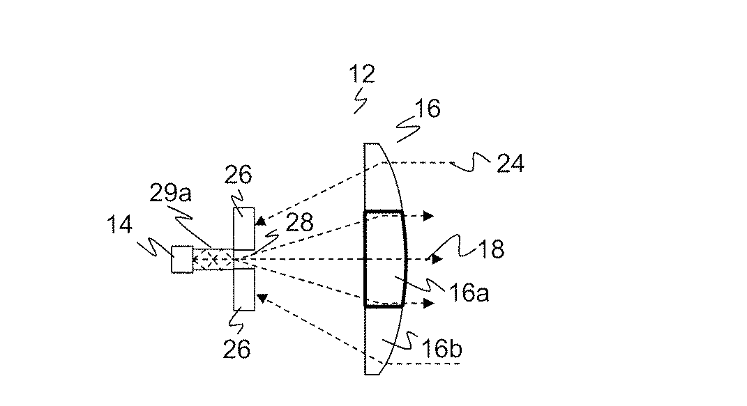
図2は送受光モジュール12の別の実施形態を示している。その構造は図1に大体対応しているが、共通の光学系16はもはや全域で同じ特性を持つ均一なレンズとして構成されてはいない。本実施形態のレンズは複領域レンズであり、発射光束18に対応する中心のレンズ部分としての発光域16aと、受信光束24に対応する外側のレンズ部分として発光域16aを取り囲む受光域16bとを備えている。この複領域レンズも一体成形された単一のレンズであることが好ましいが、領域毎に異なる光学的特性が実現され、しかもその複数の領域が好ましくは同軸に配置されている。念のため述べておくが、当然ながらこのレンズでも受信光束24の一部が中央で発光域16aに当たる。しかし、この部分は基本的に開口18内又は発光器14上で消え、検出されずに無駄になるため、本明細書では多くの箇所でこの消失部分を無視している。
FIG. 2 shows another embodiment of the light transmitting and receiving
複領域レンズにより、発射光束18と受信光束24に対してレンズの作用が異なるように調整することができる。特に、発光域16aの焦点距離を受光域16bの焦点距離とは異なるように選ぶことができる。発光域16aにおいて短い焦点距離を選べば、受光器26上での受信光束24の受光スポットが大きくなるため有利である。このようにすれば、受信光束24のうち開口28内又は発光器14上で失われる部分の相対的な割合が小さくなる。同様に考えると、普通ではない大きな受光スポットを得るためには、受光器26は受光域16bの焦点にあるべきではない。従来の見方ではそのような焦点ぼけと受光スポットの拡大は問題にならなかった。むしろ、受光器26の受光面上に小さな受光スポットを鮮明に結像させたり、更に許容差を見込んで周囲に余白となる外縁領域を残したりするよう努めていた。本発明では発光器26に対する受光器14のXY方向の調整は予め極めて高い精度で達成されているため、そのような許容差は不要である。
The multi-zone lens allows the effect of the lens to be adjusted differently for the emitted
図3は送受光モジュール12の別の実施形態を示している。図2とは異なり、ここでは発光器14が開口28の後ろではなくその中に配置されている。両者には長所と短所がある。図2の配置では開口28を相対的に小さくしておくことができる。なぜなら、発光器14の発光面だけが開口28を通じて光を発すればよいからである。図1に関する前述の数値例では、発光器14全体の寸法300μmに対して発光面は50μmであった。これには発光面の他に電子的な接触のための接続領域が必要である。その上、開口28は放射角αSを制限する絞りとして作用する。故に、図3の配置では発光器14全体を収容するために開口28を十分に大きくしなければならない。その代わり、ここでは全ての要素が一つの平面上にある。これはチップの設計と製造を容易にする。
FIG. 3 shows another embodiment of the light transmitting and receiving
図4は送受光モジュール12の別の実施形態を示している。この実施形態には開口28がない。代わりに発光器14が受光器26上で中央に配置されている。この形態は開口28が不要であるため、発光器14と受光器26のためのチップを一緒に製造することが容易である。もっとも、発光器14は受信光束24のうち比較的大きな部分を隠してしまう上、それ自身にも結合用のスペースが必要である。故にやや大きめの受光スポットが必要であり、例えば寸法が500μmのAPDでは辛うじて実現可能であるに過ぎない。それ故、例えば1mm程度の寸法を持つSPAD検出器のような大きめの受光器26を用いることが有利になり得る。
FIG. 4 shows another embodiment of the light transmitting and receiving
発光器14が開口28内にある図2及び3の実施形態では、特に開口28に必要な直径に関して短所があり得る。光学的には開口28が発射光18の光束の直径にちょうど一致することが理想的であるが、実際には様々な理由からそれより大きな開口28が必要である。まず、図3のように開口28内に発光器14を配置する場合、明白な理由として挙げられるのは、その光学的な作用面が全体の大きさより小さいという発光器14の寸法設定である。一方、開口28の後ろに発光器14を配置する場合にも、受光器26と直接接触させてはならない電導路や他の半導体材料が存在する。他の例として、端面放射型発光器を発光器14として用いる場合がある。側方へ光を射出するには受光器26の面に対して斜めの配置が必要になるため、図2のように発光器14と受光器26を直接重ねて配置することができない。
The embodiment of FIGS. 2 and 3 in which the
更に、発光器14と受光器26が空間的に隣接、場合によっては接触していると、発光器14から受光器26へ電流又は電磁場が入り込む可能性がある。このような電気的な混信があると偽の受光信号が生じ、特に1GHz以上という高い周波数域にそれが現れる。ところがこれはまさに光伝播時間の測定に是非とも使いたい周波数域である。
Furthermore, if the
別の問題点は光学的な混信である。発光器14から放射される発射光のなかには、例えば大きな発散角で放射されるため有効利用できないものがある。このような部分の光が発光効率を損なうことはほとんどないが、その光が受光器26に達して本来の受光信号を歪める恐れがある。図2のような配置は、例えば開口28の内面を経てこの混信を助長する可能性がある。
Another problem is optical interference. Some of the emitted light emitted from the
図5〜7は、発光器14と受光器26の間に一定の間隔を空けて追加の導光素子29a〜cを設けることにより前述の問題を解消又は少なくとも緩和する実施形態を示している。これらの実施形態は、発光器14を受光器26から物理的に遠ざけるという共通の考え方に基づいている。しかし、実際には開口28が発射光18の射出点又は事実上の光源となることに変わりはない。なぜなら、発光器14の発射光18は導光素子29a〜cで開口28内へ導かれるからである。更に、発光器14と受光器26は中間部品を介して間接的にマイクロメカニカルに接続されているため、調整上の利点も維持されている。
5-7 illustrate an embodiment that eliminates or at least mitigates the aforementioned problems by providing additional
事実上の光源又は仮想的な光源を受光器の近傍に生成するために用いられる導光素子29a〜cの具体的な選択のため、図5〜7は3つの例を示している。図5の導光素子29aは、ガラスやプラスチック等の透明材料で体積要素として作製された、全反射で発射光18を導く光ファイバである。図6の導光素子29bは内側が鏡面加工された中空体である。また、体積要素も鏡面を備えるものとすることができる。
FIGS. 5-7 show three examples for the specific choice of
図7の導光素子29cは結像素子として形成されている。この例では集光レンズであり、好ましくはマイクロレンズである。これにより発光器14又はその発光面の実像が開口28内に生成される。この像は図7に示した位置ではなく開口28のわずかに前又は後ろにあってもよい。
The
図8〜11は共通の光学系16として利用されるレンズの有利な発展形態を示している。このレンズは追加の円錐成分を有している。円錐成分は受光域16bのみに関わっていることが好ましい。また、平面・非球面レンズの場合、平面側を円錐形状にすること、つまりアキシコンとして構成することができる。あるいは、非球面側をいわゆる「奇数次非球面」にすることも可能である。この場合、サグ量の多項式表現には半径の偶数次の累乗だけでなく奇数次の累乗も現れる。最も簡単な場合、そのために多項式係数a1が考慮される。この係数は、a1*「レンズの中心からの距離」に比例するサグ量、つまり所望の円錐形状を生じさせる。もっとも、レンズの輪郭を適宜修正するために他の奇数次の多項式係数を用いてもよい。
8 to 11 show advantageous developments of the lenses used as the common
これについて、以下に補足として非球面方程式を再現する。
ここで、zはサグ量、rは光軸に対する垂直距離(入射高さ)、ρは頂点曲率(頂点半径R=1/ρ)、kは円錐係数、a2i、a(2i+1)はそれぞれ補正多項式の偶数次又は奇数次の係数であり、max(2n,2m+1)が多項式の次数である。
For this, the aspheric equation is reproduced as a supplement below.
Here, z is the sag amount, r is the vertical distance (incident height) to the optical axis, ρ is the apex curvature (apex radius R = 1 / ρ), k is the conic coefficient, and a 2i and a (2i + 1) are respectively corrected It is an even-order or odd-order coefficient of the polynomial, and max (2 n, 2 m + 1) is the polynomial order.
円錐成分を導入する場合、それが平面側であろうと、あるいは奇数次の多項式係数又は全く別のレンズ形状を通じたものであろうと、一つの物体点はもはや受光器26で一つの画像点に結像されず、細い円環の上に結像される。つまり、円錐成分を有するレンズは、焦点位置に依存した輪郭を持つ円形の光線プロファイルを生成する。
When introducing a conical component, one object point is no longer connected to one image point at the
図8はそれを様々な焦点位置におけるスポットプロファイルについて示している。中央のスポットプロファイルは焦点の合った配置に対応しており、理想的にはここで鮮明な円環が生じる。受光平面をレンズに近付く方向(図8では右方向)に動かすと、中心に光の穴のようなものがある「ドーナツ」又はトーラスが生じる。逆方向に動かすと光スポットが閉じ、焦点位置から遠ざかるにつれてスポットが大きくなる。この関係は多項式の係数a1の符号を変えることにより水平方向に反転させることができる。つまりこれにより、光の穴を持つトーラスと閉じた光スポットをそれぞれ鮮明な焦点位置のどちら側に形成するか選択することができる。 FIG. 8 shows that for spot profiles at various focus positions. The central spot profile corresponds to the in-focus arrangement, which ideally results in a sharp torus. Moving the light receiving plane towards the lens (right in FIG. 8) results in a "donut" or torus with something like a hole of light in the center. When moved in the reverse direction, the light spot is closed, and the spot becomes larger as it goes away from the focal position. This relationship can be reversed in the horizontal direction by changing the sign of the coefficient a 1 of the polynomial. In other words, it is possible to select on which side of the sharp focus position the torus with the light hole and the closed light spot are respectively formed.
図9は光路を再び断面図で示している。共通の光学系16のレンズの円錐成分により光の穴32を持つ円形の光線プロファイルが生じている。この穴は鮮明な焦点位置がある方向にのみ出現する。図中に受光器26の受光平面が描かれているが、これは図8の中央にある鮮明な円環に対応している。受光平面を右又は左方向へ動かした場合のスポットプロファイルが図8のどれに当たるかも同様に直ちに理解できる。既に述べたように、a1の符号を変えることで、図9の光の穴32を図中に描かれた受光平面に対してほぼ反転させることができる。
FIG. 9 shows the light path again in cross section. The conical component of the lens of the common
受光器26が鮮明な円環の平面内にある図9の配置は特に好ましい。なぜなら、受信光束24の全ての光がまだ開口の外側、又は実施形態によっては発光器14の影の外側にまっすぐ入射するからである。同時にそのためには、生成される円環が開口28を取り囲むような半径を持つように円錐成分を設計する必要がある。係数a1を通じて円錐形状を生じさせるという最も簡単な場合ではおよそ次式で円環の直径を見積もることができる。
ここで、fEは受光域16bの公称焦点距離、nはレンズの屈折率である。
The arrangement of FIG. 9 in which the
Here, f E is the nominal focal length of the
具体的な数値例としてa1に−0.005という値を選んだとする。改めて述べるが、これは受光域16bのみに関係するものであり、発光域16aでは奇数次の多項式係数の値はゼロのままであることが好ましい。残りの非球面パラメータを含むその他の寸法及びパラメータは図1に関する上記数値例と同じで、焦点距離fEは30mm、レンズの屈折率nは1.5とする。この場合、前の段落に記載の見積もりから、円環のおよその直径は2*30mm*0.005*(1.5−1)=150μmとなる。従って、図2の直径130μmの開口28を取り囲むことができる。
Suppose that a value of -0.005 is selected as a 1 as a specific numerical example. Again, this concerns only the
別の数値例として、a1に+0.01という値を選び、他の値は前の例と同じとする。この場合、円の直径は2*30mm*0.01*(1.5−1)=300μmとなる。これは、いずれも寸法が300μmである図3の大きめの開口28や図4の発光器14の影を取り囲むのにちょうど足りる。必要に応じてa1に少し大きめの値を選んでもよい。
As another numerical example, a value of +0.01 is selected for a 1 and the other values are the same as in the previous example. In this case, the diameter of the circle is 2 * 30 mm * 0.01 * (1.5-1) = 300 μm. This is just enough to surround the
これらの数値例では、無限遠の物体22だけでなくより近くに接近している物体22も光スポットを生成し、それが更に開口28内や発光器14上で完全に消えてしまわずに受光器26の感光面に当たるように、a1の符号により配慮が成されている。配置や符号の選択を誤るとそれが発生し易く、その結果、送受光モジュール12の近くに数メートルの大きさの不感域(デッドゾーン)が生じる恐れがある。
In these numerical examples, not only the
図10は、前述のようにa1が合理的に選ばれた場合の様々な物体距離についてスポット図を示している。図示した物体間隔は左から右へ無限遠、8m、4m、2mである。容易に分かるように、受光器26上での受光スポットは、無限遠にある物体22に対する鮮明な円環のままではないが、それでも中央部に達する光はその後もほとんどない。しかも、近付いた物体22の受光スポットは引き続き不鮮明化により拡大した状態で受光器26により受光される。
FIG. 10 shows spot diagrams for various object distances when a 1 is rationally selected as described above. The illustrated object intervals are from left to right at infinity, 8 m, 4 m and 2 m. As can be easily seen, the light receiving spot on the
図11は視野絞り34を追加した別の実施形態の送受光モジュール12を示している。受信光束24の受光路は絞りの位置付近に中間焦点を有している。故に、受光器26の視野を大幅に小さくして、発光器14及びその発射光束18からは発生し得ない外部光を遮るという視野絞り34としての作用が生じる。その結果、信号雑音比が明らかに向上する。
FIG. 11 shows another embodiment of the light transmitting / receiving
その際、相反する二つの利益の対立がある。まず、できるだけ多くの発射光18を視野絞り34に通すためには大きな絞り開口を非常に近くに置くことが望まれる。一方、受光の視野を効果的に縮小するには小さな絞りを受光器からある程度遠くに置く必要がある。従ってここで妥協点を見出さなければならない。
At that time, there are two conflicting interests that conflict. First, it is desirable to place the large stop very close in order to pass as much of the emitted light 18 to the
図12は、発光器14が導光素子29a〜cを介して受光器26から多少ずらされている図7〜9のような好ましい実施形態の場合は前述の対立を解決できることを示している。図12は実際には結像型の導光素子29cを有する図9の実施形態と図11の視野絞り34との組み合わせである。この場合、視野絞り34が極めて細くてもほぼ全ての発射光18がその視野絞り34を通過するような位置まで発光器14の像を開口28の前方で視野絞り34の近傍へ又はその平面内へずらすことができる。絞りが大きい場合は、発射光18を視野絞り34の場所に収束させることができるため、発光側に対する要求事項はない。
FIG. 12 illustrates that the aforementioned conflict can be resolved in the case of the preferred embodiment as in FIGS. 7-9, in which the
導光素子29a〜bとして光ファイバを用いる図7又は9の実施形態も同様に視野絞り34と組み合わせることができる。しかしその場合、発射光18の射出点を視野絞りの開口内まで移動させることはできない。なぜなら、そうすると導光素子29a〜bが受信光の邪魔になるからである。もっとも、射出点を受光器26と視野絞り34の間の領域に少し入り込ませることは十分にできる。
The embodiment of FIG. 7 or 9 using optical fibers as the
図13(a)及び(b)は受信光束24のための中間焦点を有する前述のような構成の基本的な問題を示している。図13(a)及び(b)にはそれぞれ遠方の物体22及び近接した物体22に対する受光路が描かれている。物体の接近に応じて受光焦点が共通の光学系16のレンズから離れて受光器26へ近付いてゆく。物体22が一定の距離まで近付くと受信光束24が開口28に強く収束されるため、ほぼ全ての光がそこで消えてしまい、物体22はもはや検出できなくなる。このような不感域は距離が2〜3メートルを下回ると既に生じ得る。
FIGS. 13a and 13b illustrate the basic problem of the above-described arrangement with an intermediate focus for the received
しかし、レンズの最適化によりこの近接領域の問題も解消できる。即ち、光線のうちほぼ受光焦点にある最も細いくびれ部がもはやあまり細くならず、意図的に視野絞り34を辛うじて通過できる程度の最小直径になるように、レンズの設計、特に受光域16bの設計を行う。つまり、近接した物体の場合でも受光スポットはもはや視野絞り34の絞り開口より小さくならないため、視野絞りが適切に設計されていれば受信光束24のうち十分な量の光が開口28で消えずに残る。
However, the optimization of the lens can solve the problem of the near area. That is, the design of the lens, in particular the
レンズ設計においてこの効果を得るには様々な方法が考えられる。例えば、意図的に結像誤差を残しておくことで前述のような大きな受光スポットを生じさせる。あるいは、ここでもまた非球面のパラメータa1を利用し、それを通じて焦点における光線の最小直径を調整することができる。その場合、受信光束24の断面がそれより小さくなる箇所はどこにもない。このような措置をとれば、図8〜10について説明した小さな円環の利点が視野絞り34の利点と組み合わされる。
Various methods can be considered to achieve this effect in lens design. For example, by intentionally leaving an imaging error, a large light receiving spot as described above is generated. Alternatively, again also using parameters a 1 aspheric, through which it is possible to adjust the minimum diameter of the beam at the focal point. In that case, there is no place where the cross section of the received
視野絞り34を有する実施形態についても数値例をいくつか示す。これらの例は、それと関係のある大きな物体距離に対する制限なしで最適化されている。以下、いずれも前述の例と大部分が一致するが、発光器14のチップの寸法が300μmで、発光側の放射角がαS=±15°、受光側の最大角がαE=±30°、チップの厚みが150μm、発光面が50μmである。受光器26については寸法を1mmとするが、これには計算上の役割はなく、単に受光スポットを受けるために十分な面積が利用できればよい。特に視野絞り34の絞り開口は受光器26よりも小さくしなければならない。受光スポットの大きさの見積もりとそれに続く受光効率の見積もりでは、視野絞り34が受光路の中間焦点に正確に位置しているというやや単純な仮定を行っている。
Some numerical examples are also shown for the embodiment having the
第1の例は開口28の後ろに発光器14がある図2の状況に対応している。開口28の直径は130μmで、受光器26から260μmの距離に口径280μmの視野絞り34が配置される。この場合、受光器26上の受光スポットの直径は約300μmになり、受光効率は約80%となる。
A first example corresponds to the situation of FIG. 2 with the
第2の例は開口28内に発光器14がある図3の状況に対応している。開口28の直径は300μmで、受光器26から480μmの距離に口径300μmの視野絞り34が配置される。この場合、受光器26上の受光スポットの直径は約550μmになり、受光効率は約70%となる。
A second example corresponds to the situation of FIG. 3 with the
第3の例は受光器26のすぐ前に発光器14がある図4の状況に対応している。発光器14は直径480μmの影を作る。受光器26から690μmの距離に口径340μmの視野絞り34が配置される。受光器26上の受光スポットの直径は約800μmになり、受光効率は約65%となる。
A third example corresponds to the situation of FIG. 4 in which the
図14は送受光モジュール12の別の実施形態の概略図である。この送受光モジュール12は受光器26の前に発光器14がある図4の配置に基づいているが、他の実施形態、特に図2又は3のように開口28を有する形態にも同様に適用できる。
FIG. 14 is a schematic view of another embodiment of the light transmitting and receiving
本発明に従って発光器14と受光器26を空間的に隣接させると、発光路から受光路へ直接的に光学的又は電気的な混信が起きるという問題が発生しうる。パルス式システムの場合、発光器14の作動フェーズは短く、従って混信も短い。とりわけ、例えば最大で1nsという短いパルス長を選んだ場合にそうなる。ところが近接領域では、発光器14がまだパルスを発生している間、受光器26での検出がずっと妨害され、結果的に検出能力がほぼ完全に失われてしまう。
When the
これを解決するため、図14の実施形態では近接領域用の追加の受光器26aが設けられている。この追加の受光器26aは、混信を阻止する光学的な遮蔽体36、場合によっては電気的にも有効な遮蔽体36の外側に配置されることが好ましい。例えば500mmまでの近接領域にある物体22は送受光モジュール12から見ると非常に広い範囲に発射光束18を反射するため、追加の受光器26aは専用の受光光学系がなくても十分な光を受け取る。もっとも、追加の受光レンズを増設することも考えられる。これは共通の受光光学系16と結合された二重レンズの形にしてもよいが、その場合は該レンズ内の移行部分に統合された遮蔽体を用いることが好ましい。追加の受光器26aも評価ユニット30に接続することが好ましいが、独自の電子機器によって制御及び評価を行うようにしてもよい。
To solve this, the embodiment of FIG. 14 is provided with an additional
混信を防止する又は少なくともその作用を制限するための他の対策として、既に言及したゲーティングが考えられる。あるいは、追加の受光器26aの代わりに近接領域用の別の補足センサ、例えば誘導型、容量型、磁気型、超音波型、レーダ型等のセンサを使用することも考えられる。本発明又は従来技術による構成を有する完全な光電式の追加モジュールや、別体となった追加の光電センサの使用も考えられる。
As other measures to prevent interference or at least limit its effect, the gating already mentioned can be considered. Alternatively, it is also conceivable to use another supplementary sensor for the near field, for example an inductive, capacitive, magnetic, ultrasound, radar, etc., sensor instead of the additional
図15は同軸配置の変形を有する送受光モジュール12の概略図である。厳密に言うと、同軸配置の場合は発光器14と受光器26が完全に一つの軸上にあるか、少なくともその光路が合流した後で一つの軸上に載る必要がある。この厳密な概念解釈は本発明に係る全ての実施形態に対して前提とされることが好ましい。しかし、図15で説明しているような多少広めの定義も差し当たり許容し、それを同軸と呼んでもよい。なぜなら、送受光モジュール12の外側の光路は全ての実際的な事項に関して同軸系に該当し、二軸系には該当しないからである。
FIG. 15 is a schematic view of the light transmitting and receiving
図15では発光器14と受光器26が並んでいる。しかし開口28はなお一方側に制限されている。それでも、発光器14と受光器26はやはり近接しており、その間隔は既に何度も述べたように最大で300μm又はそれ未満であるが、SPAD検出器の場合のように最大で例えば500μm又はそれより大きくなることもある。いずれにせよ、発光器14と受光器はマイクロメカニカルに相互に固定され、それにより高い精度の位置決めが可能である。
In FIG. 15, the
共通の光学系16のレンズは、発光域16aが中心にあり、受光域16bに取り囲まれているという意味では依然として同軸であるが、中心からわずかにずれていてもよい。マイクロメートルのオーダーである発光器14と受光器26の間隔とレンズまでの距離とを比較すれば、そのようなずれはほとんど実際的な影響を及ぼさない。
The lens of the common
一方、レンズの形状には好ましい相違がある。このレンズは受光域16bの範囲ではもはや回転対称ではなく、くさび形状又はプリズム特性を有している。このような変形は平面側に施すことができる。あるいは、追加的に考え得る円錐成分について既に説明したのと同様に、その補正を曲面側に統合する。図15では傾きが誇張して描かれており、実際には20ミリラジアン又は1°で十分である。この値は、焦点距離が50mm、屈折率が1.5である場合に発光器14と受光器26の間の横方向のずれ500μmにほぼ対応する。
On the other hand, there is a preferable difference in the shape of the lens. This lens is no longer rotationally symmetrical in the region of the receiving
このような配置とレンズを用いた場合、送受光モジュール12の外側における光線の進み方は同心且つ共線的である。なぜなら、送受光モジュール12内での受光路の発光路に対するわずかな傾きが受光域16bのくさび形状により補償され、実質的に同軸となるからである。ただし、発光器14と受光器26は並んでいるため、前述の厳密な概念解釈によれば同軸ではない。
When such an arrangement and a lens are used, the ray traveling on the outside of the transmitting and receiving
図16は、受光域16bに傾き特性を持つ上述の共通の光学系16を、側方に光を射出する発光器14(特に端面放射型発光器)のためにいかに利用できるかを示している。そのために、発光器14と受光器が同一平面上に並べて配置され、マイクロメカニカルに相互に結合されている。ここでは例として、共通のマイクロメカニカルな支持板35上に載置することで両者を結合している。横方向に出る発射光14はまず支持板35の面に平行に進んだ後、偏向素子37により所望の放射方向に方向転換される。その後の光路は図15とほぼ同じである。
FIG. 16 shows how the above-mentioned common
図17は送受光モジュール12の別の実施形態を示している。ここでは発光路が発光鏡胴38により遮蔽されている。これは、光学的な混信、そして場合によっては電気的な混信をも防止するためのあらゆる形態の機械的な経路分離手段を意味している。当然ながら、発光鏡胴38は、受信光束24のうち中心付近に入射して受光器26に達する可能性がある部分も妨害する。しかし、発光域16a内の光路には可逆性があるから、そのような部分はいずれにせよほとんど存在しない。
FIG. 17 shows another embodiment of the light transmitting and receiving
図18は別の実施形態を示している。この例では複数の送受光モジュール12a〜cが共通の光学系16の後ろに配置されている。送受光モジュール12a〜c同士の横方向の間隔がレンズ全体の寸法よりも明らかに小さければ、複数の発射光束18a〜cに対する一つの中央の発光域16aと複数の受信光束24に対する一つの外側の受光域16bとを有する単一のレンズを構成することがなおも可能である。なお、図18の描画は尺度が不均一であることに注意されたい。複数の送受光モジュール12a〜cと1枚のレンズの組み合わせにより非常に簡素で小型の多光線モジュールが得られる。これは例えば光格子や多重センサ、複数の操作平面を有するレーザスキャナ等に利用できる。もちろん、より多くの光線を得るために複数の多光線モジュールを互いに組み合わせることもできる。
FIG. 18 shows another embodiment. In this example, a plurality of light transmitting and receiving
図19及び20は送受光モジュール12の更に別の実施形態を示している。この実施形態は発光器14が受光器26上にある図4の配置に特に適しているが、これに限るものではない。本実施形態では受光器26と発光器14の前に追加の光学素子40が配置される。ただし、図20では幾何学的な形状が異なるためそれが発光器14の前だけにある。光学素子40は、出射する発射光束18にはその入射角及び出射角が小さいためほとんど影響を与えないような形状になっている。しかし、受信光束24については、受光器14に向かって進み、検出されずに無駄になってしまっていたはずの一部の光線24aが、その入射角がやや大きいことと、光学素子が円周状に中心を取り囲んで外へ向かって上る形状であることから、屈折して少なくとも部分的に受光器26に当たる。従って、光学素子40は、光線24aを受光器26の方へ方向転換させることにより、光線24aにとって発光器14を見えなくする一種の隠れ蓑のように作用する。これにより、発光器14及びその影のせいで失われる光の量が減る。光学素子40は例えば発光器14又は受光器26上にグラウト材として実現される。
FIGS. 19 and 20 show another embodiment of the light transmitting and receiving
本発明を実施形態に基づいて説明した。各実施形態は第一にそれぞれ特定の有利な修正に向けられているが、時には特定の修正を組み合わせて説明した。本発明は有利な修正を他のやり方で組み合わせた様々な変形も含んでいる。例えば、受光器14の配置は開口28の後ろ、開口28内又は受光器26の前から、またレンズの設計は複領域、円錐成分及び/又は焦点誤差から、それぞれ互いに十分に独立して選ぶことができる。また、距離及び絞り開口の大きさが様々に異なる視野絞り34、追加の受光器26a、又は理想的な同軸配置からわずかに逸脱した配置とそれに合った受光光学系16、発光鏡胴38及び/又は光学素子40は、追加又は省略が可能である。また、様々な形態の同種又は異種の送受光モジュール12a〜cを図18のように集めて1つの多光線モジュールにすることができる。
The present invention has been described based on the embodiments. Although each embodiment is primarily directed to specific advantageous modifications, sometimes specific combinations have been described in combination. The invention also includes various modifications that combine advantageous modifications in other ways. For example, the arrangement of the
Claims (15)
前記発光器(14)と前記受光器(16)が少なくとも間接的にマイクロメカニカルに相互に結合されていることを特徴とする送受光モジュール(12)。 A light emitter (14) having a light emission optical system (16, 16a) and a light receiver (26) having a light reception optical system (16, 16b), the emission of the emitted light (18) of the light emitter (14) The angle (α s ) is smaller than the light receiving angle (α E ) of the received light (24) incident on the light receiver (26), and the light emitter (14) and the light receiver (26) are arranged coaxially A light emitting and receiving module (12) for a photoelectric sensor (10), wherein the light emitting optical system (16, 16a) and the light receiving optical system (16, 16b) are configured as a common optical system (16);
Transmitting / receiving module (12), characterized in that said light emitter (14) and said light receiver (16) are micromechanically coupled to each other at least indirectly.
を特徴とする請求項1に記載の送受光モジュール(12)。 Transmission and reception according to claim 1, characterized in that the common optical system (16) is configured as a common lens, in particular the light emitter (14) is arranged at the focal point of the common lens. Module (12).
を特徴とする請求項2に記載の送受光モジュール(12)。 The common lens is configured as a multi-region lens having a light emission area (16a) and a light reception area (16b), and in particular, the light emission area (16a) is disposed at the center, and the light reception area (16b) The light transmitting / receiving module (12) according to claim 2, characterized in that it is arranged so as to surround it.
を特徴とする請求項3に記載の送受光モジュール(12)。 The light emitting and receiving module (12) according to claim 3, characterized in that the light emitting area (16a) has a focal length shorter than the light receiving area (16b).
を特徴とする請求項3又は4に記載の送受光モジュール(12)。 That said light receiving area (16b) comprises a conical component, in particular that the circular beam profile produced by said conical component has a central area (32) of a size corresponding to said light receiver (26) The light transmitting / receiving module (12) according to claim 3 or 4, characterized in that:
を特徴とする請求項1〜5のいずれかに記載の送受光モジュール(12)。 The light transmitting / receiving module (12) according to any of the preceding claims, characterized in that the distance between the light emitter (14) and the light receiver (26) is at most 300 m.
を特徴とする請求項1〜6のいずれかに記載の送受光モジュール(12)。 The light receiver (26) comprises an opening (28), wherein the light emitter (14) is arranged in or behind the opening, and in particular the size of the opening (28) is at most 300 μm. The light transmitting / receiving module (12) according to any one of claims 1 to 6.
を特徴とする請求項7に記載の送受光モジュール(12)。 A light guiding element (29a-c) for guiding the emitted light (18) into the opening (28) is disposed behind the opening (28) and the light emitting element (14) together with the light emitting element (14) A light transmitting and receiving module (12) according to claim 7, characterized in that the aperture is effectively a light source by being disposed between light receivers (26).
を特徴とする請求項7又は8に記載の送受光モジュール(12)。 9. A device according to claim 7 or 8, characterized in that the light guiding element comprises optical fiber elements (29a-b) or is that which generates an image of the light source in or before the opening (29c). Transmission / reception module (12) as described.
を特徴とする請求項1〜6のいずれかに記載の送受光モジュール(12)。 The light transmitting / receiving module (12) according to any of the preceding claims, wherein the light emitter (14) is arranged on the light receiver (26).
を特徴とする請求項1〜10のいずれかに記載の送受光モジュール(12)。 A field stop (34) is assigned to the common optical system (16), in particular, the received light (24) only up to the size of the stop aperture of the field stop (34). The light transmitting / receiving module (12) according to any one of claims 1 to 10, wherein the light transmitting / receiving module (12) is configured not to converge.
を特徴とする請求項1〜11のいずれかに記載の送受光モジュール(12)。 The light transmitting and receiving module (12) according to any one of claims 1 to 11, wherein the common optical system (16) has a light beam deflection characteristic to compensate for the inclination of the light receiving path with respect to the light emitting path. .
を特徴とする請求項1〜12のいずれかに記載の送受光モジュール(12)。 A light emitting barrel (38) is disposed between the light emitter (14) and the common optical system (16), and / or before the light emitter (14), the light emitter (14) 13. An optical element (40) according to any of the preceding claims, characterized in that it is arranged for deflecting the incoming light (24a) incident in the direction towards) towards the light receiver (26). Transmitting / receiving module (12).
前記受光器(14)と前記発光器(26)が少なくとも間接的にマイクロメカニカルに相互に結合されていることにより、前記受信光(24)の少なくとも一部が、前記発射光(18)が放射される箇所から最大でも500μmの近傍で受光されることを特徴とする方法。 A method for detecting an object (22) in a monitoring area (20), wherein a light emitter (14) sends out emitted light into the monitoring area (20) through a light emitting optical system (16, 16a), and a light receiver (26) receives the received light (24) together with the emitted light (18) reflected in the monitoring area (20) through the light receiving optical system (16, 16b), and emits the radiation angle of the received light (18) alpha S) of the light receiving angle (alpha E) less than the received light (24), said emitter (14) and the light receiver (26) is disposed coaxially, the light emitting optical system (16, 16a ) And the light receiving optical system (16, 16b) are configured as a common optical system (16),
The receiver (14) and the emitter (26) are micromechanically coupled to each other at least indirectly, so that at least a portion of the received light (24) is emitted by the emitted light (18). Light is received in the vicinity of at most 500 μm from the location where
Applications Claiming Priority (4)
| Application Number | Priority Date | Filing Date | Title |
|---|---|---|---|
| DE102017124535.9 | 2017-10-20 | ||
| DE102017124535.9A DE102017124535A1 (en) | 2017-10-20 | 2017-10-20 | Transceiver module for an optoelectronic sensor and method for detecting objects |
| EP18177007.4A EP3474033B1 (en) | 2017-10-20 | 2018-06-11 | Transmit-receive module for an optoelectronic sensor and method for detecting objects |
| EP18177007.4 | 2018-06-11 |
Publications (2)
| Publication Number | Publication Date |
|---|---|
| JP2019105623A true JP2019105623A (en) | 2019-06-27 |
| JP6736629B2 JP6736629B2 (en) | 2020-08-05 |
Family
ID=62599488
Family Applications (1)
| Application Number | Title | Priority Date | Filing Date |
|---|---|---|---|
| JP2018197512A Active JP6736629B2 (en) | 2017-10-20 | 2018-10-19 | Transmitting/receiving module for photoelectric sensor and object detecting method |
Country Status (5)
| Country | Link |
|---|---|
| US (1) | US20190120962A1 (en) |
| EP (1) | EP3474033B1 (en) |
| JP (1) | JP6736629B2 (en) |
| CN (1) | CN109696688A (en) |
| DE (1) | DE102017124535A1 (en) |
Cited By (3)
| Publication number | Priority date | Publication date | Assignee | Title |
|---|---|---|---|---|
| JP2023512528A (en) * | 2020-01-30 | 2023-03-27 | ロベルト・ボッシュ・ゲゼルシャフト・ミト・ベシュレンクテル・ハフツング | Transmission unit and LIDAR device with improved optical efficiency |
| JP2023116279A (en) * | 2022-02-09 | 2023-08-22 | 株式会社小糸製作所 | Emitter, receiver and measuring device |
| WO2025205473A1 (en) * | 2024-03-27 | 2025-10-02 | 北陽電機株式会社 | Optical ranging device |
Families Citing this family (70)
| Publication number | Priority date | Publication date | Assignee | Title |
|---|---|---|---|---|
| US11609336B1 (en) | 2018-08-21 | 2023-03-21 | Innovusion, Inc. | Refraction compensation for use in LiDAR systems |
| FR3056524B1 (en) * | 2016-09-28 | 2018-10-12 | Valeo Systemes D'essuyage | DETECTION SYSTEM FOR MOTOR VEHICLE |
| US11300683B2 (en) | 2016-12-30 | 2022-04-12 | Innovusion Ireland Limited | Multiwavelength LiDAR design |
| US10942257B2 (en) | 2016-12-31 | 2021-03-09 | Innovusion Ireland Limited | 2D scanning high precision LiDAR using combination of rotating concave mirror and beam steering devices |
| US11009605B2 (en) | 2017-01-05 | 2021-05-18 | Innovusion Ireland Limited | MEMS beam steering and fisheye receiving lens for LiDAR system |
| US10969475B2 (en) | 2017-01-05 | 2021-04-06 | Innovusion Ireland Limited | Method and system for encoding and decoding LiDAR |
| US11054508B2 (en) | 2017-01-05 | 2021-07-06 | Innovusion Ireland Limited | High resolution LiDAR using high frequency pulse firing |
| DE102017117694A1 (en) * | 2017-08-04 | 2019-02-07 | Sick Ag | Opto-electronic sensor and method for detecting objects in a surveillance area |
| EP3470872B1 (en) * | 2017-10-11 | 2021-09-08 | Melexis Technologies NV | Sensor device |
| WO2019079642A1 (en) | 2017-10-19 | 2019-04-25 | Innovusion Ireland Limited | Lidar with large dynamic range |
| US11493601B2 (en) | 2017-12-22 | 2022-11-08 | Innovusion, Inc. | High density LIDAR scanning |
| WO2019139895A1 (en) | 2018-01-09 | 2019-07-18 | Innovusion Ireland Limited | Lidar detection systems and methods that use multi-plane mirrors |
| US11675050B2 (en) | 2018-01-09 | 2023-06-13 | Innovusion, Inc. | LiDAR detection systems and methods |
| US11927696B2 (en) | 2018-02-21 | 2024-03-12 | Innovusion, Inc. | LiDAR systems with fiber optic coupling |
| WO2019165130A1 (en) | 2018-02-21 | 2019-08-29 | Innovusion Ireland Limited | Lidar detection systems and methods with high repetition rate to observe far objects |
| WO2019165289A1 (en) | 2018-02-22 | 2019-08-29 | Innovusion Ireland Limited | Receive path for lidar system |
| WO2019165095A1 (en) | 2018-02-23 | 2019-08-29 | Innovusion Ireland Limited | Distributed lidar systems |
| CN112292608B (en) | 2018-02-23 | 2024-09-20 | 图达通智能美国有限公司 | 2D Manipulation Systems for LIDAR Systems |
| WO2020013890A2 (en) | 2018-02-23 | 2020-01-16 | Innovusion Ireland Limited | Multi-wavelength pulse steering in lidar systems |
| US11567182B2 (en) | 2018-03-09 | 2023-01-31 | Innovusion, Inc. | LiDAR safety systems and methods |
| US11289873B2 (en) | 2018-04-09 | 2022-03-29 | Innovusion Ireland Limited | LiDAR systems and methods for exercising precise control of a fiber laser |
| WO2019199796A1 (en) | 2018-04-09 | 2019-10-17 | Innovusion Ireland Limited | Compensation circuitry for lidar receiver systems and method of use thereof |
| DE102018209394A1 (en) * | 2018-06-13 | 2019-12-19 | Robert Bosch Gmbh | Coaxial LiDAR system |
| CN112585492B (en) | 2018-06-15 | 2024-10-25 | 图达通智能美国有限公司 | LIDAR system and method for focusing on a range of interest |
| US11860316B1 (en) | 2018-08-21 | 2024-01-02 | Innovusion, Inc. | Systems and method for debris and water obfuscation compensation for use in LiDAR systems |
| US11579300B1 (en) | 2018-08-21 | 2023-02-14 | Innovusion, Inc. | Dual lens receive path for LiDAR system |
| US11614526B1 (en) | 2018-08-24 | 2023-03-28 | Innovusion, Inc. | Virtual windows for LIDAR safety systems and methods |
| US11796645B1 (en) | 2018-08-24 | 2023-10-24 | Innovusion, Inc. | Systems and methods for tuning filters for use in lidar systems |
| US11579258B1 (en) | 2018-08-30 | 2023-02-14 | Innovusion, Inc. | Solid state pulse steering in lidar systems |
| US12313788B1 (en) | 2018-10-09 | 2025-05-27 | Seyond, Inc. | Ultrashort pulses in LiDAR systems |
| CN114114606B (en) | 2018-11-14 | 2024-09-06 | 图达通智能美国有限公司 | LIDAR systems and methods using polygonal mirrors |
| DE112020000407B4 (en) | 2019-01-10 | 2024-02-15 | Innovusion, Inc. | LIDAR SYSTEMS AND METHODS WITH RADIATION DEFLECTION AND WIDE ANGLE SIGNAL DETECTION |
| US11486970B1 (en) | 2019-02-11 | 2022-11-01 | Innovusion, Inc. | Multiple beam generation from a single source beam for use with a LiDAR system |
| US11977185B1 (en) | 2019-04-04 | 2024-05-07 | Seyond, Inc. | Variable angle polygon for use with a LiDAR system |
| CN110456373A (en) * | 2019-08-30 | 2019-11-15 | 上海禾赛光电科技有限公司 | The receiving circuit of laser radar, laser radar and laser radar ranging method |
| CN110471078B (en) * | 2019-09-25 | 2023-06-30 | 浙江缔科新技术发展有限公司 | Light quantum height measurement telescope and height measurement method |
| DE102019125906A1 (en) * | 2019-09-26 | 2021-04-01 | Blickfeld GmbH | Emitter array for light detection and distance measurement, LIDAR |
| CN110613401A (en) * | 2019-10-31 | 2019-12-27 | 珠海格力电器股份有限公司 | Dust detection device and dust collector |
| WO2021083016A1 (en) * | 2019-11-01 | 2021-05-06 | 上海禾赛科技股份有限公司 | Laser radar and method for performing detection by using same |
| CN110865386B (en) * | 2019-12-12 | 2025-07-04 | 武汉徕得智能技术有限公司 | Laser optical path system and laser distance measuring device |
| CN111221031B (en) * | 2020-01-21 | 2021-08-24 | 中国工程物理研究院流体物理研究所 | A collimator for measuring the effective area of a Si-PIN detector and a method of using the same |
| WO2021184381A1 (en) * | 2020-03-20 | 2021-09-23 | 华为技术有限公司 | Ranging system and vehicle |
| EP3885789A1 (en) * | 2020-03-26 | 2021-09-29 | Leica Geosystems AG | Distance measuring device |
| CN111398974A (en) * | 2020-04-10 | 2020-07-10 | 广东博智林机器人有限公司 | Laser detection device |
| IT202000007837A1 (en) * | 2020-04-14 | 2021-10-14 | Tecnosens S P A | NON-CONTACT DIMENSIONAL MEASURING DEVICE WITH MICROMETRIC RESOLUTION |
| DE102020113647A1 (en) | 2020-05-20 | 2021-11-25 | Blickfeld GmbH | Optical System for Light Detection and Ranging, LIDAR |
| CN112731314B (en) * | 2020-12-21 | 2024-03-19 | 北京仿真中心 | Vehicle-mounted radar and visible light combined detection simulation device |
| CN112835017B (en) * | 2020-12-31 | 2022-11-18 | 武汉万集信息技术有限公司 | Scanning system of multi-line laser radar, multi-line laser radar and scanning method |
| CN112800559B (en) * | 2021-02-02 | 2024-03-08 | 中海石油(中国)有限公司 | A sensor arrangement method and system |
| US12061289B2 (en) | 2021-02-16 | 2024-08-13 | Innovusion, Inc. | Attaching a glass mirror to a rotating metal motor frame |
| US11422267B1 (en) | 2021-02-18 | 2022-08-23 | Innovusion, Inc. | Dual shaft axial flux motor for optical scanners |
| EP4260086B1 (en) | 2021-03-01 | 2024-11-27 | Seyond, Inc. | Fiber-based transmitter and receiver channels of light detection and ranging systems |
| US11555895B2 (en) | 2021-04-20 | 2023-01-17 | Innovusion, Inc. | Dynamic compensation to polygon and motor tolerance using galvo control profile |
| US11614521B2 (en) | 2021-04-21 | 2023-03-28 | Innovusion, Inc. | LiDAR scanner with pivot prism and mirror |
| US11662439B2 (en) | 2021-04-22 | 2023-05-30 | Innovusion, Inc. | Compact LiDAR design with high resolution and ultra-wide field of view |
| WO2022225859A1 (en) | 2021-04-22 | 2022-10-27 | Innovusion, Inc. | A compact lidar design with high resolution and ultra-wide field of view |
| CN115327555A (en) | 2021-05-10 | 2022-11-11 | 信泰光学(深圳)有限公司 | Optical device |
| TWI792305B (en) * | 2021-05-10 | 2023-02-11 | 大陸商信泰光學(深圳)有限公司 | Optical device with coaxial optical path |
| EP4314885A1 (en) | 2021-05-12 | 2024-02-07 | Innovusion, Inc. | Systems and apparatuses for mitigating lidar noise, vibration, and harshness |
| CN117413199A (en) | 2021-05-21 | 2024-01-16 | 图达通智能美国有限公司 | Mobile profiles for smart scanning using the galvanometer mirror inside the LIDAR scanner |
| WO2023278761A1 (en) * | 2021-07-01 | 2023-01-05 | Banner Engineering Corp. | Photoelectric sensor boresighting improvement |
| US11768294B2 (en) | 2021-07-09 | 2023-09-26 | Innovusion, Inc. | Compact lidar systems for vehicle contour fitting |
| CN113687335B (en) * | 2021-08-16 | 2025-04-22 | 昆山丘钛微电子科技股份有限公司 | A lens module testing structure, method and device |
| US12468017B2 (en) | 2021-10-15 | 2025-11-11 | Seyond, Inc. | Integrated mirror motor galvanometer |
| CN216356147U (en) | 2021-11-24 | 2022-04-19 | 图达通智能科技(苏州)有限公司 | Vehicle-mounted laser radar motor, vehicle-mounted laser radar and vehicle |
| US11871130B2 (en) | 2022-03-25 | 2024-01-09 | Innovusion, Inc. | Compact perception device |
| US12204033B2 (en) | 2022-03-25 | 2025-01-21 | Seyond, Inc. | Multimodal detection with integrated sensors |
| CN114719750A (en) * | 2022-03-30 | 2022-07-08 | 北京烁科精微电子装备有限公司 | Wafer side cut position detection device |
| EP4375702A1 (en) * | 2022-11-23 | 2024-05-29 | Scantinel Photonics GmbH | Device for scanning fmcw lidar range measurement |
| CN115856912B (en) * | 2023-02-06 | 2023-05-30 | 宜科(天津)电子有限公司 | Data processing system for detecting movement direction of object |
Citations (7)
| Publication number | Priority date | Publication date | Assignee | Title |
|---|---|---|---|---|
| JPS5922017A (en) * | 1982-06-30 | 1984-02-04 | イ−ストマン コダック カンパニ− | Apparatus for determining distance of object |
| JPS616782U (en) * | 1984-06-19 | 1986-01-16 | 誠幹 西川 | light wave distance meter |
| US20030066954A1 (en) * | 2001-09-03 | 2003-04-10 | Sick Ag | Optoelectronic detection device |
| US20060001859A1 (en) * | 2004-06-26 | 2006-01-05 | Lutz Lohmann | Optical sensor |
| US20060109450A1 (en) * | 2004-11-19 | 2006-05-25 | Yi Liu | Laser distance measuring device |
| EP2312919A1 (en) * | 2009-10-08 | 2011-04-20 | Sick Ag | Optoelectronic sensor |
| US20170269215A1 (en) * | 2016-03-19 | 2017-09-21 | Velodyne Lidar, Inc. | Integrated Illumination And Detection For LIDAR Based 3-D Imaging |
Family Cites Families (16)
| Publication number | Priority date | Publication date | Assignee | Title |
|---|---|---|---|---|
| DE19757849C5 (en) | 1997-12-24 | 2013-11-21 | Sick Ag | Scanner and device for the optical detection of obstacles, and their use |
| DE19860464C2 (en) * | 1998-12-28 | 2001-02-01 | Jenoptik Jena Gmbh | Laser distance measuring device for large measuring ranges |
| JP4121803B2 (en) * | 2002-08-08 | 2008-07-23 | 株式会社トプコン | Lightwave distance measuring device |
| US7894044B1 (en) * | 2008-03-11 | 2011-02-22 | Oceanit Laboratories, Inc. | Laser for coherent LIDAR |
| CN101430377B (en) * | 2008-11-18 | 2011-06-22 | 北京航空航天大学 | APD array-based non-scanning 3D imaging lidar optical system |
| US20110293215A1 (en) * | 2010-03-30 | 2011-12-01 | Anthony Ruggiero | Low loss laser transmission through telescopes with mirror obscurations |
| EP2607924A1 (en) * | 2011-12-23 | 2013-06-26 | Leica Geosystems AG | Distance sensor adjustment |
| US9651417B2 (en) * | 2012-02-15 | 2017-05-16 | Apple Inc. | Scanning depth engine |
| DE102012025281A1 (en) * | 2012-12-21 | 2014-06-26 | Valeo Schalter Und Sensoren Gmbh | Optical object detection device with a MEMS and motor vehicle with such a detection device |
| EP2860497B2 (en) | 2013-10-09 | 2019-04-10 | SICK STEGMANN GmbH | Optoelectronic sensor and method for manufacturing the same |
| DE102014105781B4 (en) * | 2014-04-24 | 2016-04-07 | Sick Ag | Optoelectronic sensor and method for acquiring measurement information from a surveillance area |
| CN104330843A (en) * | 2014-07-22 | 2015-02-04 | 凯迈(洛阳)环测有限公司 | Laser ceilometer optical system and light-splitting reflector thereof |
| US10088557B2 (en) * | 2015-03-20 | 2018-10-02 | MSOTEK Co., Ltd | LIDAR apparatus |
| DE102015112656A1 (en) * | 2015-07-31 | 2017-02-02 | Sick Ag | Distance sensor |
| DE102015121839A1 (en) * | 2015-12-15 | 2017-06-22 | Sick Ag | Optoelectronic sensor and method for detecting an object |
| DE102016114995A1 (en) * | 2016-03-30 | 2017-10-05 | Triple-In Holding Ag | Apparatus and method for taking distance images |
-
2017
- 2017-10-20 DE DE102017124535.9A patent/DE102017124535A1/en not_active Withdrawn
-
2018
- 2018-06-11 EP EP18177007.4A patent/EP3474033B1/en active Active
- 2018-10-18 US US16/164,217 patent/US20190120962A1/en not_active Abandoned
- 2018-10-18 CN CN201811212765.6A patent/CN109696688A/en active Pending
- 2018-10-19 JP JP2018197512A patent/JP6736629B2/en active Active
Patent Citations (8)
| Publication number | Priority date | Publication date | Assignee | Title |
|---|---|---|---|---|
| JPS5922017A (en) * | 1982-06-30 | 1984-02-04 | イ−ストマン コダック カンパニ− | Apparatus for determining distance of object |
| US4511248A (en) * | 1982-06-30 | 1985-04-16 | Eastman Kodak Company | Active electro-optical distance detection methods and devices |
| JPS616782U (en) * | 1984-06-19 | 1986-01-16 | 誠幹 西川 | light wave distance meter |
| US20030066954A1 (en) * | 2001-09-03 | 2003-04-10 | Sick Ag | Optoelectronic detection device |
| US20060001859A1 (en) * | 2004-06-26 | 2006-01-05 | Lutz Lohmann | Optical sensor |
| US20060109450A1 (en) * | 2004-11-19 | 2006-05-25 | Yi Liu | Laser distance measuring device |
| EP2312919A1 (en) * | 2009-10-08 | 2011-04-20 | Sick Ag | Optoelectronic sensor |
| US20170269215A1 (en) * | 2016-03-19 | 2017-09-21 | Velodyne Lidar, Inc. | Integrated Illumination And Detection For LIDAR Based 3-D Imaging |
Cited By (4)
| Publication number | Priority date | Publication date | Assignee | Title |
|---|---|---|---|---|
| JP2023512528A (en) * | 2020-01-30 | 2023-03-27 | ロベルト・ボッシュ・ゲゼルシャフト・ミト・ベシュレンクテル・ハフツング | Transmission unit and LIDAR device with improved optical efficiency |
| JP7385048B2 (en) | 2020-01-30 | 2023-11-21 | ロベルト・ボッシュ・ゲゼルシャフト・ミト・ベシュレンクテル・ハフツング | Transmission unit and LIDAR device with improved optical efficiency |
| JP2023116279A (en) * | 2022-02-09 | 2023-08-22 | 株式会社小糸製作所 | Emitter, receiver and measuring device |
| WO2025205473A1 (en) * | 2024-03-27 | 2025-10-02 | 北陽電機株式会社 | Optical ranging device |
Also Published As
| Publication number | Publication date |
|---|---|
| US20190120962A1 (en) | 2019-04-25 |
| EP3474033A1 (en) | 2019-04-24 |
| EP3474033B1 (en) | 2020-04-22 |
| JP6736629B2 (en) | 2020-08-05 |
| DE102017124535A1 (en) | 2019-04-25 |
| CN109696688A (en) | 2019-04-30 |
Similar Documents
| Publication | Publication Date | Title |
|---|---|---|
| JP6736629B2 (en) | Transmitting/receiving module for photoelectric sensor and object detecting method | |
| US10739460B2 (en) | Time-of-flight detector with single-axis scan | |
| US9285266B2 (en) | Object detector including a light source with light emitting region of a first size in a first direction and a second size in a second direction | |
| US10996322B2 (en) | Lidar sensor | |
| US9316495B2 (en) | Distance measurement apparatus | |
| US20200355801A1 (en) | Transmitting device for a lidar scanner having a scanning mirror covered by a cover element | |
| JP2014029317A (en) | Laser radar device | |
| JP2004521355A (en) | Optical distance measuring device | |
| CN110312947B (en) | Lidar sensor for detecting objects | |
| JP2020034547A (en) | Photoelectric sensor and object detection method | |
| US6603534B2 (en) | Laser range finder for large ranges of measurement with a special receiver | |
| WO2020116078A1 (en) | Laser radar | |
| US6281968B1 (en) | Laser distance-measuring instrument for large measuring ranges | |
| US12487335B2 (en) | Receiving system for lidar, lidar and method for inhibiting ghost lines | |
| US20070030474A1 (en) | Optical range finder | |
| JP3947159B2 (en) | Sensor device for quick optical distance measurement according to the confocal optical imaging principle | |
| CN110140060B (en) | Optical component for a lidar system, lidar system and working device | |
| CN108885260B (en) | Time-of-flight detector with single axis scanning | |
| US11486967B2 (en) | Module for a lidar sensor and lidar sensor | |
| US11762066B2 (en) | Multi-beam scanning system | |
| CN110596673A (en) | Coaxial laser radar system | |
| US5815272A (en) | Filter for laser gaging system | |
| JP2000147311A (en) | Positioning method in optical waveguide coupling device and optical waveguide coupling device realized using the same | |
| CN113030912B (en) | Laser radar system based on scanning galvanometer | |
| US20250189635A1 (en) | Light source module including an optical path and a method of operating the light source module |
Legal Events
| Date | Code | Title | Description |
|---|---|---|---|
| A621 | Written request for application examination |
Free format text: JAPANESE INTERMEDIATE CODE: A621 Effective date: 20190212 |
|
| A977 | Report on retrieval |
Free format text: JAPANESE INTERMEDIATE CODE: A971007 Effective date: 20200228 |
|
| A131 | Notification of reasons for refusal |
Free format text: JAPANESE INTERMEDIATE CODE: A131 Effective date: 20200310 |
|
| A521 | Request for written amendment filed |
Free format text: JAPANESE INTERMEDIATE CODE: A523 Effective date: 20200609 |
|
| TRDD | Decision of grant or rejection written | ||
| A01 | Written decision to grant a patent or to grant a registration (utility model) |
Free format text: JAPANESE INTERMEDIATE CODE: A01 Effective date: 20200714 |
|
| A61 | First payment of annual fees (during grant procedure) |
Free format text: JAPANESE INTERMEDIATE CODE: A61 Effective date: 20200715 |
|
| R150 | Certificate of patent or registration of utility model |
Ref document number: 6736629 Country of ref document: JP Free format text: JAPANESE INTERMEDIATE CODE: R150 |
|
| R250 | Receipt of annual fees |
Free format text: JAPANESE INTERMEDIATE CODE: R250 |
|
| R250 | Receipt of annual fees |
Free format text: JAPANESE INTERMEDIATE CODE: R250 |
|
| R250 | Receipt of annual fees |
Free format text: JAPANESE INTERMEDIATE CODE: R250 |