JP2019080457A - Non-contact power supply device - Google Patents
Non-contact power supply device Download PDFInfo
- Publication number
- JP2019080457A JP2019080457A JP2017207127A JP2017207127A JP2019080457A JP 2019080457 A JP2019080457 A JP 2019080457A JP 2017207127 A JP2017207127 A JP 2017207127A JP 2017207127 A JP2017207127 A JP 2017207127A JP 2019080457 A JP2019080457 A JP 2019080457A
- Authority
- JP
- Japan
- Prior art keywords
- power
- antenna
- power transmission
- power receiving
- receiving antenna
- Prior art date
- Legal status (The legal status is an assumption and is not a legal conclusion. Google has not performed a legal analysis and makes no representation as to the accuracy of the status listed.)
- Withdrawn
Links
- 230000005540 biological transmission Effects 0.000 claims abstract description 190
- 238000003860 storage Methods 0.000 claims abstract description 23
- 239000000758 substrate Substances 0.000 claims description 51
- 239000000463 material Substances 0.000 claims description 31
- 239000010949 copper Substances 0.000 claims description 21
- RYGMFSIKBFXOCR-UHFFFAOYSA-N Copper Chemical compound [Cu] RYGMFSIKBFXOCR-UHFFFAOYSA-N 0.000 claims description 20
- 229910052802 copper Inorganic materials 0.000 claims description 20
- 239000011347 resin Substances 0.000 claims description 6
- 229920005989 resin Polymers 0.000 claims description 6
- 238000010586 diagram Methods 0.000 abstract description 7
- 238000000034 method Methods 0.000 description 15
- 230000006870 function Effects 0.000 description 12
- 238000004519 manufacturing process Methods 0.000 description 10
- 230000005684 electric field Effects 0.000 description 9
- PXHVJJICTQNCMI-UHFFFAOYSA-N Nickel Chemical compound [Ni] PXHVJJICTQNCMI-UHFFFAOYSA-N 0.000 description 7
- 239000010408 film Substances 0.000 description 7
- 239000000696 magnetic material Substances 0.000 description 7
- 239000004020 conductor Substances 0.000 description 6
- 239000011521 glass Substances 0.000 description 6
- 230000000694 effects Effects 0.000 description 5
- 230000005674 electromagnetic induction Effects 0.000 description 5
- 239000003822 epoxy resin Substances 0.000 description 4
- 239000010931 gold Substances 0.000 description 4
- 229920000647 polyepoxide Polymers 0.000 description 4
- XEEYBQQBJWHFJM-UHFFFAOYSA-N Iron Chemical compound [Fe] XEEYBQQBJWHFJM-UHFFFAOYSA-N 0.000 description 3
- BQCADISMDOOEFD-UHFFFAOYSA-N Silver Chemical compound [Ag] BQCADISMDOOEFD-UHFFFAOYSA-N 0.000 description 3
- 238000009713 electroplating Methods 0.000 description 3
- PCHJSUWPFVWCPO-UHFFFAOYSA-N gold Chemical compound [Au] PCHJSUWPFVWCPO-UHFFFAOYSA-N 0.000 description 3
- 229910052737 gold Inorganic materials 0.000 description 3
- 230000005389 magnetism Effects 0.000 description 3
- 229910052759 nickel Inorganic materials 0.000 description 3
- 238000000206 photolithography Methods 0.000 description 3
- 238000007747 plating Methods 0.000 description 3
- 229920000139 polyethylene terephthalate Polymers 0.000 description 3
- 239000005020 polyethylene terephthalate Substances 0.000 description 3
- 229910052709 silver Inorganic materials 0.000 description 3
- 239000004332 silver Substances 0.000 description 3
- 238000004544 sputter deposition Methods 0.000 description 3
- 239000010409 thin film Substances 0.000 description 3
- 229920000178 Acrylic resin Polymers 0.000 description 2
- 239000004925 Acrylic resin Substances 0.000 description 2
- ZOXJGFHDIHLPTG-UHFFFAOYSA-N Boron Chemical compound [B] ZOXJGFHDIHLPTG-UHFFFAOYSA-N 0.000 description 2
- 229910000990 Ni alloy Inorganic materials 0.000 description 2
- VYPSYNLAJGMNEJ-UHFFFAOYSA-N Silicium dioxide Chemical compound O=[Si]=O VYPSYNLAJGMNEJ-UHFFFAOYSA-N 0.000 description 2
- XUIMIQQOPSSXEZ-UHFFFAOYSA-N Silicon Chemical compound [Si] XUIMIQQOPSSXEZ-UHFFFAOYSA-N 0.000 description 2
- MCMNRKCIXSYSNV-UHFFFAOYSA-N Zirconium dioxide Chemical compound O=[Zr]=O MCMNRKCIXSYSNV-UHFFFAOYSA-N 0.000 description 2
- HZEWFHLRYVTOIW-UHFFFAOYSA-N [Ti].[Ni] Chemical compound [Ti].[Ni] HZEWFHLRYVTOIW-UHFFFAOYSA-N 0.000 description 2
- 229910045601 alloy Inorganic materials 0.000 description 2
- 239000000956 alloy Substances 0.000 description 2
- 229910052782 aluminium Inorganic materials 0.000 description 2
- XAGFODPZIPBFFR-UHFFFAOYSA-N aluminium Chemical compound [Al] XAGFODPZIPBFFR-UHFFFAOYSA-N 0.000 description 2
- 229910052796 boron Inorganic materials 0.000 description 2
- 230000000747 cardiac effect Effects 0.000 description 2
- 229910017052 cobalt Inorganic materials 0.000 description 2
- 239000010941 cobalt Substances 0.000 description 2
- GUTLYIVDDKVIGB-UHFFFAOYSA-N cobalt atom Chemical compound [Co] GUTLYIVDDKVIGB-UHFFFAOYSA-N 0.000 description 2
- 238000005530 etching Methods 0.000 description 2
- 239000007943 implant Substances 0.000 description 2
- 229910010272 inorganic material Inorganic materials 0.000 description 2
- 239000011147 inorganic material Substances 0.000 description 2
- 229910052751 metal Inorganic materials 0.000 description 2
- 239000002184 metal Substances 0.000 description 2
- 230000010355 oscillation Effects 0.000 description 2
- 239000005011 phenolic resin Substances 0.000 description 2
- -1 polyethylene terephthalate Polymers 0.000 description 2
- 229910001285 shape-memory alloy Inorganic materials 0.000 description 2
- 238000007493 shaping process Methods 0.000 description 2
- 229910052710 silicon Inorganic materials 0.000 description 2
- 239000010703 silicon Substances 0.000 description 2
- 239000010935 stainless steel Substances 0.000 description 2
- 229910001220 stainless steel Inorganic materials 0.000 description 2
- 230000000638 stimulation Effects 0.000 description 2
- 229910000859 α-Fe Inorganic materials 0.000 description 2
- 229910018072 Al 2 O 3 Inorganic materials 0.000 description 1
- PIGFYZPCRLYGLF-UHFFFAOYSA-N Aluminum nitride Chemical compound [Al]#N PIGFYZPCRLYGLF-UHFFFAOYSA-N 0.000 description 1
- HBBGRARXTFLTSG-UHFFFAOYSA-N Lithium ion Chemical compound [Li+] HBBGRARXTFLTSG-UHFFFAOYSA-N 0.000 description 1
- 229910052779 Neodymium Inorganic materials 0.000 description 1
- 229910052581 Si3N4 Inorganic materials 0.000 description 1
- CDBYLPFSWZWCQE-UHFFFAOYSA-L Sodium Carbonate Chemical compound [Na+].[Na+].[O-]C([O-])=O CDBYLPFSWZWCQE-UHFFFAOYSA-L 0.000 description 1
- ATJFFYVFTNAWJD-UHFFFAOYSA-N Tin Chemical compound [Sn] ATJFFYVFTNAWJD-UHFFFAOYSA-N 0.000 description 1
- PNEYBMLMFCGWSK-UHFFFAOYSA-N aluminium oxide Inorganic materials [O-2].[O-2].[O-2].[Al+3].[Al+3] PNEYBMLMFCGWSK-UHFFFAOYSA-N 0.000 description 1
- 239000005388 borosilicate glass Substances 0.000 description 1
- 239000003990 capacitor Substances 0.000 description 1
- 230000008859 change Effects 0.000 description 1
- 238000005229 chemical vapour deposition Methods 0.000 description 1
- 238000000576 coating method Methods 0.000 description 1
- 210000003298 dental enamel Anatomy 0.000 description 1
- 238000007772 electroless plating Methods 0.000 description 1
- 230000004907 flux Effects 0.000 description 1
- 229910052742 iron Inorganic materials 0.000 description 1
- 238000000608 laser ablation Methods 0.000 description 1
- 229910001416 lithium ion Inorganic materials 0.000 description 1
- 239000007769 metal material Substances 0.000 description 1
- 230000004048 modification Effects 0.000 description 1
- 238000012986 modification Methods 0.000 description 1
- 210000003205 muscle Anatomy 0.000 description 1
- QEFYFXOXNSNQGX-UHFFFAOYSA-N neodymium atom Chemical compound [Nd] QEFYFXOXNSNQGX-UHFFFAOYSA-N 0.000 description 1
- 239000011368 organic material Substances 0.000 description 1
- 230000000149 penetrating effect Effects 0.000 description 1
- 238000005498 polishing Methods 0.000 description 1
- 229920003217 poly(methylsilsesquioxane) Polymers 0.000 description 1
- 229920001721 polyimide Polymers 0.000 description 1
- 239000009719 polyimide resin Substances 0.000 description 1
- 239000004800 polyvinyl chloride Substances 0.000 description 1
- 238000002360 preparation method Methods 0.000 description 1
- 230000008569 process Effects 0.000 description 1
- 229910052594 sapphire Inorganic materials 0.000 description 1
- 239000010980 sapphire Substances 0.000 description 1
- HBMJWWWQQXIZIP-UHFFFAOYSA-N silicon carbide Chemical compound [Si+]#[C-] HBMJWWWQQXIZIP-UHFFFAOYSA-N 0.000 description 1
- 229910010271 silicon carbide Inorganic materials 0.000 description 1
- HQVNEWCFYHHQES-UHFFFAOYSA-N silicon nitride Chemical compound N12[Si]34N5[Si]62N3[Si]51N64 HQVNEWCFYHHQES-UHFFFAOYSA-N 0.000 description 1
- 229910052814 silicon oxide Inorganic materials 0.000 description 1
- 239000000126 substance Substances 0.000 description 1
- 239000011135 tin Substances 0.000 description 1
- 229910052718 tin Inorganic materials 0.000 description 1
- HGCGQDMQKGRJNO-UHFFFAOYSA-N xenon monochloride Chemical compound [Xe]Cl HGCGQDMQKGRJNO-UHFFFAOYSA-N 0.000 description 1
Images




Landscapes
- Coils Of Transformers For General Uses (AREA)
- Charge And Discharge Circuits For Batteries Or The Like (AREA)
Abstract
【課題】小型化が可能でかつ安価な非接触給電装置を提供する。【解決手段】非接触給電装置10は、電源部205と、ループ状に配置された第1の送電アンテナ231および第1の送電アンテナと電気的に接続され、第1の送電アンテナの周りに複数設けられた第2の送電アンテナ233を含み、電源部と接続された送電アンテナ部230と、を含む送電装置200と、蓄電部110と、ループ状に配置された第1の受電アンテナ131を含み、蓄電部と接続された受電アンテナ部130と、を含む受電装置100と、を有する。第2の送電アンテナは、第1の送電アンテナに対して直交して配置され、送電アンテナ部と受電アンテナ部とは、平行に配置される。【選択図】図1PROBLEM TO BE SOLVED: To provide a non-contact power feeding device capable of miniaturization and inexpensive. SOLUTION: A contactless power feeding device 10 is electrically connected to a power supply unit 205, a first power transmission antenna 231 arranged in a loop, and a first power transmission antenna, and a plurality of non-contact power transmission devices 10 are around the first power transmission antenna. Includes a second power transmission antenna 233 provided, a power transmission device 200 including a power transmission antenna unit 230 connected to a power supply unit, a power storage unit 110, and a first power reception antenna 131 arranged in a loop. It has a power receiving device 100 including a power receiving antenna unit 130 connected to the power storage unit. The second power transmission antenna is arranged orthogonally to the first power transmission antenna, and the power transmission antenna unit and the power reception antenna unit are arranged in parallel. [Selection diagram] Fig. 1
Description
本発明は、非接触給電装置に関する。 The present invention relates to a noncontact power feeding device.
近年、非接触方式の給電方法を用いた電子機器が広く用いられている。非接触給電の場合、送電アンテナと受電アンテナとが対向するように受電装置を含む電子機器を送電装置(給電機器)上に載置することによって、送電アンテナから受電アンテナに電力が伝送される。受電アンテナで発生した電力は、電子機器の二次電池に蓄電される。 BACKGROUND In recent years, electronic devices using a noncontact power feeding method are widely used. In the case of non-contact power feeding, power is transmitted from the power transmitting antenna to the power receiving antenna by mounting the electronic device including the power receiving device on the power transmitting device (power feeding device) such that the power transmitting antenna and the power receiving antenna face each other. The power generated by the power receiving antenna is stored in the secondary battery of the electronic device.
従来の非接触給電の場合、電界または磁界の影響が電子機器の他の電子部品に及ばないように、例えば、送電アンテナの一方の側に対して遮蔽材を設け、電界または磁界を遮蔽する必要がある。しかしながら、遮蔽材として金属板が用いられた場合、電子機器、または給電機器の小型化に伴い、金属板がアンテナの近傍に配置されると、送電されるまたは受電される電界または磁界も小さくなり、十分に給電できなくなる場合がある。一方で、遮蔽材として磁性体材料が用いられた場合、遮蔽材がアンテナの近傍に配置されても電界または磁界は小さくならず保持される。しかしながら、磁性体材料は高価であるため、アンテナの製造コストが高くなってしまう。 In the case of conventional non-contact power feeding, for example, it is necessary to provide a shielding material on one side of the power transmission antenna to shield the electric field or the magnetic field so that the influence of the electric field or the magnetic field does not affect other electronic components of the electronic device. There is. However, when a metal plate is used as the shielding material, when the metal plate is disposed in the vicinity of the antenna along with the miniaturization of the electronic device or the feeding device, the electric field or magnetic field to be transmitted or received becomes smaller. , It may not be possible to supply power enough. On the other hand, when a magnetic material is used as the shielding material, the electric field or the magnetic field is not reduced even if the shielding material is arranged in the vicinity of the antenna. However, since the magnetic material is expensive, the manufacturing cost of the antenna is increased.
上記課題を鑑み、本発明は、小型化が可能で、かつ安価な非接触給電装置を提供することを目的の一つとする。 In view of the above problems, an object of the present invention is to provide a non-contact power feeding apparatus which can be miniaturized and which is inexpensive.
本発明の一実施形態によれば、電源部と、ループ状に配置された第1の送電アンテナおよび第1の送電アンテナと電気的に接続され、第1の送電アンテナの周りに複数設けられた第2の送電アンテナを含み、電源部と接続された送電アンテナ部と、を含む送電装置と、蓄電部と、ループ状に配置された第1の受電アンテナを含み、蓄電部と接続された受電アンテナ部と、を含む受電装置と、を含み、第2の送電アンテナは、第1の送電アンテナに対して直交して配置され、送電アンテナ部と受電アンテナ部とは、平行に配置される、非接触給電装置が、提供される。 According to an embodiment of the present invention, a plurality of power supply units are electrically connected to the first power transmitting antenna and the first power transmitting antenna arranged in a loop and provided around the first power transmitting antenna. A power transmission device including a second power transmission antenna and including a power transmission antenna unit connected to a power supply unit, a power storage unit, and a first power receiving antenna arranged in a loop, and a power reception unit connected to the power storage unit And a second power transmitting antenna is disposed orthogonal to the first power transmitting antenna, and the power transmitting antenna and the power receiving antenna are disposed in parallel. A contactless power supply is provided.
上記非接触給電装置において、受電アンテナ部は、第1の受電アンテナと電気的に接続され、第1の受電アンテナの周りに複数設けられた第2の受電アンテナを含み、第2の受電アンテナは、第1の受電アンテナに対して直交して配置されてもよい。 In the non-contact power feeding apparatus, the power receiving antenna unit includes a second power receiving antenna electrically connected to the first power receiving antenna and provided in a plurality around the first power receiving antenna, and the second power receiving antenna is , And may be disposed orthogonal to the first power receiving antenna.
上記非接触給電装置において、第2の送電アンテナの大きさは、第1の送電アンテナよりも小さく、第2の受電アンテナの大きさは、第1の受電アンテナよりも小さくてもよい。 In the non-contact power feeding device, the size of the second power transmitting antenna may be smaller than that of the first power transmitting antenna, and the size of the second power receiving antenna may be smaller than that of the first power receiving antenna.
上記非接触給電装置において、第2の送電アンテナの巻き数は、第1の送電アンテナの巻き数よりも多く、第2の受電アンテナの巻き数は、第1の受電アンテナの巻き数よりも多くてもよい。 In the noncontact power feeding apparatus, the number of turns of the second power transmitting antenna is larger than the number of turns of the first power transmitting antenna, and the number of turns of the second power receiving antenna is larger than the number of turns of the first power receiving antenna May be
上記非接触給電装置において、送電装置は、断面視において、第1面と、第1面と反対側の第2面とを有し、受電装置は、断面視において、第1面と対向する第3面と、第3面と反対側の第4面とを有し、送電アンテナ部の第1面側の磁力は、第2面側の磁力と異なり、受電アンテナ部の第3面側の磁力は、第4面側の磁力と異なってもよい。 In the above non-contact power feeding device, the power transmission device has a first surface and a second surface opposite to the first surface in a cross sectional view, and the power receiving device faces the first surface in a cross sectional view The magnetic force on the first surface side of the power transmitting antenna unit is different from the magnetic force on the second surface side, and the magnetic force on the third surface side of the power receiving antenna unit has three surfaces and the fourth surface opposite to the third surface. May be different from the magnetic force on the fourth surface side.
上記非接触給電装置において、第1面側の磁力は、第2面側の磁力よりも強くてもよい。 In the non-contact power feeding device, the magnetic force on the first surface side may be stronger than the magnetic force on the second surface side.
上記非接触給電装置において、送電アンテナ部は、第1基板をさらに含み、第2の送電アンテナは、第1面側に第1上部配線、第1基板内に第1貫通配線、および第2面側に第1下部配線を含み、第1上部配線と第1下部配線とは第1貫通配線を介して接続され、受電アンテナ部は、第2基板をさらに含み、第2の受電アンテナは、第3面側に第2上部配線、第2基板内に第2貫通配線、および第4面側に第2下部配線を含み、第2上部配線と第2下部配線とは第2貫通配線を介して接続される、第2上部配線と第2下部配線とは第2貫通配線を介して接続されてもよい。 In the non-contact power feeding apparatus, the power transmission antenna unit further includes a first substrate, and the second power transmission antenna has a first upper wiring on the first surface side, a first through wiring in the first substrate, and a second surface. The first upper wiring and the first lower wiring are connected via the first through wiring, the power receiving antenna unit further includes the second substrate, and the second power receiving antenna is The third upper surface includes the second upper wiring, the second substrate includes the second through wiring, and the fourth surface includes the second lower wiring, and the second upper wiring and the second lower wiring are connected via the second through wiring. The second upper wiring and the second lower wiring to be connected may be connected via the second through wiring.
上記非接触給電装置において、第1の送電アンテナは、第2の送電アンテナおよび第2の送電アンテナのそれぞれを接続する第1接続配線を含み、第1の受電アンテナは、第2の受電アンテナおよび第2の受電アンテナのそれぞれを接続する第2接続配線を含んでもよい。 In the non-contact power feeding apparatus, the first power transmission antenna includes a first connection wire connecting the second power transmission antenna and the second power transmission antenna, and the first power receiving antenna is a second power receiving antenna and You may include the 2nd connection wiring which connects each of a 2nd power receiving antenna.
上記非接触給電装置において、第1基板および第2基板の少なくともいずれかは、樹脂材料を含んでもよい。 In the non-contact power feeding device, at least one of the first substrate and the second substrate may include a resin material.
上記非接触給電装置において、第1貫通配線および第2貫通配線の少なくともいずれかは、銅を含んでもよい。 In the non-contact power feeding device, at least one of the first through wiring and the second through wiring may include copper.
以下、本出願で開示される発明の各実施形態について、図面を参照しつつ説明する。但し、本発明は、その要旨を逸脱しない範囲において様々な形態で実施することができ、以下に例示する実施形態の記載内容に限定して解釈されるものではない。 Hereinafter, embodiments of the invention disclosed in the present application will be described with reference to the drawings. However, the present invention can be implemented in various forms without departing from the scope of the present invention, and the present invention is not interpreted as being limited to the description of the embodiments exemplified below.
なお、本実施形態で参照する図面において、同一部分または同様な機能を有する部分には同一の符号または類似の符号(数字の後に−1、−2等を付しただけの符号)を付し、その繰り返しの説明は省略する場合がある。また、図面の寸法比率は説明の都合上実際の比率とは異なったり、構成の一部が図面から省略されたりする場合がある。 In the drawings referred to in this embodiment, the same portions or portions having similar functions are denoted by the same reference numerals or similar reference numerals (reference numerals with only -1, -2, etc. appended after numbers), The repeated description may be omitted. Further, the dimensional ratio of the drawings may be different from the actual ratio for convenience of explanation, or part of the configuration may be omitted from the drawings.
<第1実施形態>
以下、本発明の一実施形態の非接触給電装置について説明する。
First Embodiment
Hereafter, the non-contact electric power supply of one Embodiment of this invention is demonstrated.
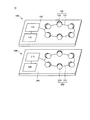
図1は、非接触給電装置10の模式図である。非接触給電装置10は、送電装置200および受電装置100を含む。
FIG. 1 is a schematic view of the non-contact
(1−1.送電装置の構成)
図1に示すように、送電装置200は、電源部205、制御部210、送電アンテナ部230および支持部240を含む。電源部205、制御部210および送電アンテナ部230は、支持部240の表面または内部に設けられる。なお、電源部205は、支持部240の外側に配置されてもよい。電源部205、制御部210および送電アンテナ部230は電気的に接続される。
(1-1. Configuration of power transmission device)
As shown in FIG. 1, the
電源部205には、例えば、交流電源が用いられる。なお、電源部205が、携帯型電源である場合には、直流電源が用いられてもよい。
For the
送電アンテナ部230は、制御部210からの命令に従い、電界または磁界を介して受電装置100に電力を供給する。
Power
支持部240は、電源部205、制御部210、および送電アンテナ部230を支持する機能を有する。支持部240は、筐体と言い換えることができる。支持部240には、例えばポリエチレンテレフタレート(PET)、ポリ塩化ビニル(PVC)などの樹脂材料が用いられる。支持部240は、上面240Aおよび下面240B(後述する図2にて記載)を有する。下面240Bは、上面240Aの反対側に設けられた面である。支持部240の厚さは、数百μmから数十cmの間で目的に応じて適宜選択される。
The
送電アンテナ部230は、送電アンテナ231および送電アンテナ233を有する。送電アンテナ231および送電アンテナ233は、電磁誘導方式のアンテナであり、ループアンテナとも呼ばれる。送電するための電流が送電アンテナ231および送電アンテナ233に送られ、磁界が発生する。送電アンテナ部230は、例えば短波(HF)や極超短波(UHF)の周波数帯域で共振するように構成される。具体的には、短波は13.56MHzの周波数帯域に相当する。また、極超短波は、860〜960MHz、さらに数GHzの周波数帯域に相当する。
The power
送電アンテナ231および送電アンテナ233には、抵抗率が低い材料が用いられる。例えば、送電アンテナ231および送電アンテナ233には銅(Cu)が用いられる。銅は、展延性が高く、加工しやすいためアンテナの材料として望ましい。なお、送電アンテナ231および送電アンテナ233には、銅に限定されず、アルミニウム(Al)、銀(Ag)、金(Au)などの抵抗率が低い材料が用いられてもよい。また、送電アンテナ231および送電アンテナ233には、鉄(Fe)、ニッケル(Ni)、コバルト(Co)、フェライトなど、磁性を有する導電体が用いられてもよい。また、磁性を有する導電体は、単体でもよいし、合金でもよい。また、磁性を有する導電体にホウ素を含んでもよい。また、チタンニッケル合金などの形状記憶合金、さらにステンレスなどが送電アンテナ231および送電アンテナ233に用いられてもよい。送電アンテナ231および送電アンテナ233の表面にはエナメルなどの被覆材が設けられてもよい。
For the
(1−2.受電装置の構成)
図1に示すように、受電装置100は、蓄電部110、制御部119、受電アンテナ部130および支持部140を含む。蓄電部110、制御部119、および受電アンテナ部130は、支持部140の表面または内部に設けられる。蓄電部110、制御部119および受電アンテナ部130は電気的に接続される。
(1-2. Configuration of power reception device)
As shown in FIG. 1,
受電アンテナ部130は、送電装置200から電界または磁界を介して受けた電力を蓄電部110、制御部119に送る。
Power
蓄電部110は、供給された電力を蓄電するバッテリ(二次電池)として機能する。蓄電部110には、例えばリチウムイオン電池が用いられる。
支持部140は、蓄電部110、制御部119、および受電アンテナ部130を支持する機能を有する。支持部140には、支持部240と同様の材料が用いられてもよい。支持部140の厚さは、数百μmから数cmの間で目的に応じて適宜選択される。
受電アンテナ部130は、受電アンテナ131および受電アンテナ133を有する。受電アンテナ部130は、送電アンテナ部230と同様の構成を有する。受電アンテナ131および受電アンテナ133は、電磁誘導方式のアンテナであり、ループアンテナである。受電アンテナ131および受電アンテナ133に囲まれた領域を通過する磁束密度の変化に応じた大きさの起電力(電圧)が受電アンテナ部130に発生する。発生した電圧は蓄電部110に与えられる。結果として、受電装置100が用いられた電子機器が駆動する。
The power
(1−3.アンテナ部の構成)
以下に、送電装置200の送電アンテナ部230および受電装置100の受電アンテナ部130について説明する。
(1-3. Configuration of antenna unit)
Hereinafter, the power
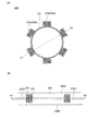
図2(A)は、送電アンテナ部230の上面図である。図2(B)は、送電アンテナ部230の上面図A1−A2間の断面図である。
FIG. 2A is a top view of the power
図2(A)および図2(B)に示すように、送電アンテナ231(第1の送電アンテナという場合がある)は、ループ状に配置される。なお、送電アンテナ231は、図2(A)に示す形状に限定されず、複数回巻く構成でもよい。送電アンテナ233(第2の送電アンテナという場合がある)は、送電アンテナ231の周りに複数個配置される。この例では、送電アンテナ231の外側に6つの送電アンテナ233が等間隔で配置される。また、送電アンテナ233は、送電アンテナ231よりも小さいものが用いられる。送電アンテナ231と、送電アンテナ233とは電気的に接続される。この例では、送電アンテナ231および複数の送電アンテナ233は、1本の配線を加工成型することで構成されている(具体的には、一筆書きのように構成される)。このとき、送電アンテナ233の一(送電アンテナ233A)とアンテナの他の一(送電アンテナ233B)とを結ぶ部分が送電アンテナ231となる。
As shown in FIGS. 2A and 2B, the power transmission antenna 231 (which may be referred to as a first power transmission antenna) is arranged in a loop. The
また、図2(B)に示すように、送電アンテナ233の中心233Cは、送電アンテナ231が配置された平面231Sに設けられる。また、送電アンテナ233は、送電アンテナ231の平面231Sに対して直交して配置される。この配置とすることにより、詳細は後述するが支持部240の上面240A側と下面240B側との間で磁力の差を設ける上でより大きな効果を得ることができる。
Moreover, as shown to FIG. 2 (B),
なお、上記の構成に限定されずに、送電アンテナ233は配置されてもよい。例えば、送電アンテナ233の中心233Cは、平面231Sから離れて配置されてもよい。また、製造工程等の影響などにより、送電アンテナ233は、送電アンテナ231の平面231Sに対して略直交して配置されてもよい。この場合の略直交するとは、直交した状態から1度以上20度以下で上側または下側に傾斜した状態をいう。また、送電アンテナ233は、必ずしも等間隔ではなく局在して配置されてもよい。
In addition, it is not limited to said structure, The
図2(A)および図2(B)に示すように、送電アンテナ233は、送電アンテナ231よりも小さい。この場合、送電アンテナ233の磁場(磁力)を高めるために、送電アンテナ233の巻き数は、送電アンテナ231の巻き数よりも多いほうが望ましい。これにより、送電アンテナ233における磁場(磁力)が高められる。
As shown in FIGS. 2A and 2B, the
図3(A)は、受電装置100の受電アンテナ部130の上面図である。図3(B)は、受電アンテナ部130の上面図A1−A2間の断面図である。
FIG. 3A is a top view of the power receiving
受電アンテナ部130は、送電装置200の送電アンテナ部230と同様の構成を有する。図3(A)および図3(B)に示すように、受電アンテナ131(第1の受電アンテナという場合がある)は、ループ状に配置される。なお、受電アンテナ131は、図3(A)に示す形状に限定されず、複数回巻く構成でもよい。受電アンテナ133(第2の受電アンテナという場合がある)は、受電アンテナ131の周りに複数個配置される。この例では、受電アンテナ131の外側に6つの受電アンテナ133が等間隔で配置される。また、受電アンテナ133は、受電アンテナ131よりも小さいものが用いられる。受電アンテナ131と、受電アンテナ133とは電気的に接続される。この例では、受電アンテナ131および複数の受電アンテナ133は、1本の配線を加工成型することで構成されている(具体的には、一筆書きのように構成される)。このとき、受電アンテナ133の一(受電アンテナ133A)とアンテナの他の一(受電アンテナ133B)とを結ぶ部分が受電アンテナ131となる。
The power
また、図3(B)に示すように、受電アンテナ133の中心133Cは、受電アンテナ131が配置された平面131Sに設けられる。また、受電アンテナ133は、受電アンテナ131の平面131Sに対して直交して配置される。
Further, as shown in FIG. 3B, the
図3(A)および図3(B)に示すように、受電アンテナ133は、受電アンテナ131よりも小さい。この場合、受電アンテナ133の磁場(磁力)を高めるために、受電アンテナ133の巻き数は、受電アンテナ131の巻き数よりも多いほうが望ましい。これにより、受電アンテナ133における磁場(磁力)が高められる。
As shown in FIGS. 3A and 3B, the
上記構造とすることで、受電アンテナ部130に送電アンテナ部230からの磁場が影響して誘導電流が流れる。
With the above-described structure, the magnetic field from the power
図4は、送電装置200の送電アンテナ部230および受電装置100の受電アンテナ部130の配置を示す断面図である。図4において、受電装置100の上面(支持部140の上面140A)と、送電装置200の上面(支持部240の上面240A)とは対向して配置されている。このとき、図4に示すように、送電アンテナ部230と受電アンテナ部130とは、平行に配置されている。この構成とすることにより、電磁誘導方式により送電装置200から受電装置100へ電力が送られる際に、電力損失を抑えることができる。また、上記において、受電アンテナ部130のうち受電アンテナ133は、送電アンテナ部230のうち送電アンテナ233と巻き方が逆になるように配置されている。これにより、受電装置100の上面側に磁界が発生することを抑えることができる。
FIG. 4 is a cross-sectional view showing the arrangement of the power transmitting
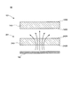
図5および図6は、送電アンテナ部230における磁力線を示す模式図である。図5に示すように、平面231Sより下方の領域R1において、送電アンテナ231の磁力線M231は、上方向に向いているのに対して、送電アンテナ233の磁力線M233は下方向に向いている。そのため、送電アンテナ231の磁力線M231と、送電アンテナ233の磁力線M233とが領域R1において干渉する。したがって、領域R1においては、送電アンテナ231の磁力線M231が邪魔される。一方、平面231Sより上方の領域R2において、送電アンテナ231の磁力線M231および送電アンテナ233の磁力線M233は、ともに上方向に向いている。したがって、領域R2においては、送電アンテナ231の磁力線M231が邪魔されない。したがって、図6に示すように、送電アンテナ部230において、平面231Sより下方、つまり支持部240の下面240Bの磁力より、平面231Sより上方、つまり支持部240の上面240A側の磁力は大きい。つまり、送電アンテナ部230の上面240A側の磁力は、下面240B側の磁力と異なっているということができる。
5 and 6 are schematic diagrams showing magnetic lines of force in the power
なお、受電装置100の受電アンテナ部130も同様の構成を有する。したがって、受電アンテナ部130の上面140A側の磁力は、下面140B側の磁力と異なっているということができる。
The power
(1−4.受電装置のブロック図)
次に、図7(A)に、受電装置100のブロック図を示す。
(1-4. Block diagram of power reception device)
Next, FIG. 7A shows a block diagram of the
受電装置100は、蓄電部110、制御部119、および受電アンテナ部130の他、電圧リミット回路111、整流回路113、記憶部121、抵抗123、および負荷部125などを有することができる。
The
電圧リミット回路111は、受電アンテナ部130において過大な電圧が誘起された場合に、入力される電圧から受電装置100を保護する機能を有する。過大な電圧が誘起された場合、発生する電流のうち不要な部分は抵抗123を用いて熱に変換され、外部へ放出される。
The
整流回路113は、受電アンテナ部130において誘起される交流電流を直流電流へ変換する機能を有する。整流回路113により直流となった電源電圧は、受電装置100を構成するすべての回路に供給される。
The
制御部119は、受電に関する機能全体を制御する機能を有する。制御部119は種々の論理回路によって構成される。制御部119には、CPU(Central Processing Unit)などが用いられてもよい。
The
記憶部121には、受電に関するデータを記憶するためのメモリ素子が備えられる。なお、記憶部121は、必ずしも設けられなくてもよい。
The
負荷部125は、電力を物理的動作に変換する機能を有する。負荷部125として、例えばアクチュエータが用いられる。なお、負荷部125は必ずしも設けられなくてもよい。
The
(1−5.送電装置のその他の構成)
図7(B)に送電装置200の構成例を示す。送電装置200は、電源部205、制御部210、および送電アンテナ部230の他、記憶部213、発振回路220、および送信回路225を含む。
(1-5. Other Configurations of Power Transmission Device)
The structural example of the
制御部210は、送電装置200全体を制御する。制御部210は、記憶部213を用いて、送電時間、送電電力量を制御する。制御部210は、CPUとともにメモリなどが用いられてもよい。
The
発振回路220は、電源部205からの電力をもとに電力伝送に用いる周波数の信号を生成する機能を有する。搬送波として、例えば13.56MHzの高周波が生成される。なお、搬送波は、これに限定されず、110kHz〜205kHzの周波数信号を用いてもよいし、高周波(2.45GHz)の信号が用いられてもよい。
The
送信回路225は、信号の増幅、不要な周波数の減衰などを行い、送信すべき周波数のみを取り出す。また、送信回路225は、送電電力の生成を行う。また、送信回路225は、コイルやコンデンサを用いた共振回路を含んでもよい。
The
(1−6.非接触給電装置10の動作)
次に、非接触給電装置10の動作について説明する。図8は、非接触給電装置10の駆動時の断面図である。
(Operation of non-contact power feeding device 10)
Next, the operation of the non-contact
図8に示すように、受電装置100の上面(支持部140の上面140A)を下側、下面(支持部140の下面140B)を上側にした状態で、送電装置200を駆動させる。送電装置200が駆動すると、交流信号が送電アンテナ部230に加えられ、磁場M231が発生する(搬送波)。この磁場M231が受電装置100の受電アンテナ部130を通過する。このとき、誘導起電力が働くことにより送電装置200から受電装置100に電力が供給される。
As shown in FIG. 8, the
このとき、図6において示したように、磁力線M231Bは非対称な磁気特性、つまり送電装置200の下面側よりも上面側に強い磁場を生じる。言い換えれば、送電装置200の下面側に生じる磁場を弱めることができる。
At this time, as shown in FIG. 6, the magnetic lines of force M 231 B generate asymmetric magnetic characteristics, that is, a stronger magnetic field on the upper surface side than the lower surface side of the
ここで、図19に従来の非接触給電装置50の断面図を示す。非接触給電装置50は、送電装置201および受電装置101のほかに遮蔽材190を含む。送電装置201は、送電アンテナ部230のうち送電アンテナ233を含まない。受電装置101は、受電アンテナ部130のうち受電アンテナ133を含まない。例えば、送電装置201が小さい場合、磁性体材料ではない金属材料を含む遮蔽材190が送電アンテナ部230の近傍に配置されると、送電される磁界または電界も小さくなってしまう。これにより、受電装置101が十分に給電されない場合がある。そのため、受電装置101が給電されるように支持部240と遮蔽材190との間の空間を広く設ける必要があり、送電装置201の小型化が制限される。また、磁性体材料が遮蔽材に用いられた場合、遮蔽材がアンテナの近傍に配置されても、送電される電界または磁界は、小さくならず保持される。しかしながら、磁性体材料は高価であるため、アンテナの製造コストが高くなってしまう。
Here, FIG. 19 shows a cross-sectional view of the conventional non-contact
一方、本実施形態を用いることにより、非接触給電装置10は遮蔽材を設けなくてもよい。また、遮蔽材を設けた場合でも余分な空間を設ける必要がない。したがって、送電装置200の小型化、つまり非接触給電装置の小型化を図ることができる。また、本実施形態を用いることにより、磁性体材料を含む遮蔽材を用いた場合と同様の効果を有することができる。つまり、安価に非接触給電装置を提供することができる。また、本実施形態を用いることにより、非対称な磁気特性を有することから、高い指向性を有する非接触給電装置を提供することができる。
On the other hand, by using this embodiment, the non-contact
<第2実施形態>
以下に第1実施形態と構造の異なるアンテナ部について説明する。
Second Embodiment
An antenna unit having a different structure from that of the first embodiment will be described below.
(2−1.アンテナ部の構成)
図9(A)は、送電装置200の送電アンテナ部230−1の上面図である。図9(B)は、送電アンテナ部230−1のうち送電アンテナ233−1の斜視図である。図9(A)および図9(B)に示すように、送電アンテナ部230−1は、基板245、接続配線232、および送電アンテナ233−1を有する。送電アンテナ233−1の一(送電アンテナ233−1A)と送電アンテナ233−1の他の一(送電アンテナ233−1B)とを結ぶ部分を接続配線232とした場合、233−1と232とを合わせて送電アンテナ231−1としてもよい。
(2-1. Configuration of antenna unit)
FIG. 9A is a top view of the power transmission antenna unit 230-1 of the
図9(B)に示すように、送電アンテナ233−1は、上部配線235、下部配線236および貫通配線237を含む。上部配線235および下部配線236は、貫通配線237を介して電気的に接続される。
As shown in FIG. 9B, the power transmission antenna 233-1 includes an
基板245は、支持部240の内側に設けられてもよいし、支持部240の代替として設けられてもよい。基板245には、高抵抗な材料が用いられる。例えば、基板245にはガラス・エポキシ樹脂基板が用いられる。なお、基板245は、ガラス・エポキシ樹脂に限定されず、アクリル樹脂、ポリエチレンテレフタレート樹脂などの樹脂材料が用いられてもよいし、紙基材にフェノール樹脂を含有させて硬化させた紙フェノール樹脂基板が用いられてもよい。
The
また、基板245は、石英ガラス基板、ソーダガラス基板、ホウ珪酸ガラス基板、無アルカリガラス基板、サファイア基板、シリコン基板、炭化シリコン基板、アルミナ(Al2O3)基板、窒化アルミニウム(AlN)基板、ジルコニア(ZrO2)基板などの無機材料が用いられてもよい。
The
上部配線235は、基板245の上面245Aに配置される。上部配線235は、抵抗の低い材料が用いられる。例えば、上部配線235には銅が用いられる。
The
なお、上部配線235は、銅に限定されず、アルミニウム、銀、金などの抵抗率が低い材料が用いられてもよい。また、鉄、ニッケル、コバルト、フェライトなどの磁性を有する導電体を含んでもよい。また、磁性を有する導電体は、単体でもよいし、合金でもよい。また、上部配線235は、磁性を有する導電体にホウ素を含んでもよい。また、上部配線235には、磁性体に限定されずに、チタンニッケル合金などの形状記憶合金、さらにステンレスなどが用いられてもよい。
The
下部配線236は、基板245の下面245Bに配置される。下部配線236には、上部配線235と同様の材料が用いられる。
The
貫通配線237は、基板245に設けられる。貫通配線237には、銅が用いられる。なお、貫通配線237は、銅に限定されず、金、銀、銅、ニッケルまたは錫を含む材料が用いられてもよい。
The through
図10(A)は、受電装置100の受電アンテナ部130−1の上面図である。図10(B)は、受電アンテナ部130−1の斜視図である。図10(A)および図10(B)に示すように、受電アンテナ部130−1は、基板145、接続配線132、および受電アンテナ133−1を有する。受電アンテナ133−1の一(受電アンテナ133−1A)と受電アンテナ133−1の他の一(受電アンテナ133−1B)とを結ぶ部分を接続配線132とした場合、133−1と132とを合わせて受電アンテナ131−1としてもよい。受電アンテナ部130−1は、送電アンテナ部230−1と同様の構成を有する。受電アンテナ部130−1のうち、受電アンテナ133−1は、上面145A側に上部配線135、基板145内に貫通配線137、および下面145B側に下部配線136を含む。上部配線135と下部配線136とは貫通配線137を介して接続される。
FIG. 10A is a top view of the power receiving antenna portion 130-1 of the
(2−2.アンテナ部の製造方法)
次に、送電アンテナ部230−1のうち送電アンテナ233−1の製造方法について説明する。なお、受電アンテナ部130−1の受電アンテナ133−1も同様の方法により形成される。
(2-2. Manufacturing method of antenna unit)
Next, a method of manufacturing the power transmission antenna 233-1 of the power transmission antenna unit 230-1 will be described. The power receiving antenna 133-1 of the power receiving antenna unit 130-1 is also formed by the same method.
まず、図11に示すように、基板245に貫通孔247を形成する。
First, as shown in FIG. 11, the through
基板245には、高抵抗な材料が用いられる。例えば、基板245にはガラス・エポキシ樹脂などの樹脂材料が用いられる。
For the
貫通孔247は、基板245に対してドリルなどを用いた機械的加工により形成される。貫通孔247の直径は、10μm以上1000μm以下で適宜設定される。
The through
なお、貫通孔247は、レーザー照射法(レーザーアブレーション法と呼ぶことができる)により形成されてもよい。レーザーには、エキシマレーザー、ネオジウム:ヤグレーザー(Nd:YAG)等が用いられる。例えば、エキシマレーザーにおいて塩化キセノンを用いる場合、波長が308nmの光が照射される。また、貫通孔247は、シリコン基板やガラス基板を用いた場合にはフォトリソグラフィ法およびエッチング法を用いて形成されてもよい。
The through
次に、図12に示すように貫通孔247に貫通配線237を形成する。貫通配線237には、銅が用いられる。貫通配線237は、電解めっき法または無電解めっき法により形成されてもよい。例えば、銅を用いて、貫通配線237を形成する場合、スパッタリング法により銅の薄膜を形成する。次に、銅薄膜をシード層として、電解めっき法により銅膜を形成する。最後に、基板245の上面245Aおよび下面245Bに形成された銅膜を化学機械研磨(CMP:Chemical Mechanical Polishing)法により、基板245の上面245Aおよび下面245B上の銅を除去することにより、貫通配線237が充填形成される。
Next, as shown in FIG. 12, the through
次に、図13に示すように、基板245の上面245A側に接続配線232および上部配線235を形成する。接続配線232および上部配線235には、銅が用いられる。接続配線232および上部配線235は、例えばめっき法により形成される。接続配線232および上部配線235がめっき法により形成される場合、例えば以下の方法が用いられてもよい。まず、銅の薄膜(シード層)をスパッタリング法により形成する。次に、シード層上にレジスト膜を形成後、レジスト膜をフォトリソグラフィ法などを用いて所定の形状に加工する。次に、露出したシード層上に接続配線232および上部配線235を形成する。接続配線232および上部配線235は、電解めっき法により銅膜が形成される。最後に、レジスト膜およびレジスト膜下のシード層が除去される。
Next, as shown in FIG. 13, the
なお、上部配線235は、めっき法に限定されず、印刷法、スパッタリング、CVD法、塗布法などにより形成されてもよい。このとき、上部配線235は、フォトリソグラフィ法およびエッチング法により所定の形状に加工されればよい。
The
次に、基板245の下面245Bに下部配線236を形成する。下部配線236は、上部配線235と同様の材料および方法により形成されてもよい。
Next, the
以上の方法により、送電装置200の送電アンテナ部230−1が製造される。上記製造方法を用いることにより、送電アンテナ部230のうち送電アンテナ233−1を基板245の厚さで制御することができる。このとき、基板245の厚さを薄くすることで送電アンテナ部230をさらに小さくすることができる。送電アンテナ部230が小さくなることにより、送電装置200の小型化を図ることができる。また、上記方法は、受電装置100の受電アンテナ部130にも適用される。したがって、受電アンテナ部130を小さくすることができ、受電装置100も小さくすることができる。また、本実施形態においても遮蔽材は用いなくてもよい。したがって、上記製造方法を用いることにより、非接触給電装置を小さくかつ安価に製造することができる。
The power transmission antenna unit 230-1 of the
<第3実施形態>
本実施形態では、第1実施形態において説明した非接触給電装置の具体例について説明する。
Third Embodiment
In this embodiment, a specific example of the non-contact power feeding device described in the first embodiment will be described.
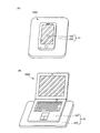
図14乃至図17は、非接触給電装置を説明する図である。非接触給電装置は、例えば、精密電子機器のほか、医療器具、産業用装置、自動車などの様々な場面において用いられる。図14(A)は、スマートフォン1000の模式図である。図14(B)は、ノート型パーソナルコンピュータ2000の模式図である。図15は、ID(Identification)カード3000の模式図である。
FIG. 14 to FIG. 17 illustrate the non-contact power feeding device. The non-contact power feeding device is used, for example, in various scenes such as medical instruments, industrial devices, automobiles, as well as precision electronic devices. FIG. 14A is a schematic view of the
図16は、人体に設けられた医療機器のうち、人口内耳4000、心臓ペースメーカ5000、筋肉等に埋め込まれた生体電気刺激装置6000の模式図である。
FIG. 16 is a schematic view of a
図17(A)は、産業用ロボットの模式図である。このとき、受電装置100は、回転部7100に設けられる。図17(B)は、乗用車8000の模式図である。
FIG. 17A is a schematic view of an industrial robot. At this time, the
本発明の実施形態として上述した各実施形態は、相互に矛盾しない限りにおいて、適宜組み合わせて実施することができる。また、各実施形態を基にして、当業者が適宜構成要素の追加、削除もしくは設計変更を行ったものも、本発明の要旨を備えている限り、本発明の範囲に含まれる。 The embodiments described above as the embodiments of the present invention can be implemented in combination as appropriate as long as they do not contradict each other. In addition, those to which a person skilled in the art appropriately adds, deletes, or changes the design of components based on each embodiment are also included in the scope of the present invention as long as the gist of the present invention is included.
また、上述した各実施形態によりもたらされる作用効果とは異なる他の作用効果であっても、本明細書の記載から明らかなもの、又は、当業者において容易に予測し得るものについては、当然に本発明によりもたらされるものと理解される。 In addition, even if other functions and effects different from the functions and effects provided by the above-described embodiments are apparent from the description of the present specification or those that can be easily predicted by those skilled in the art, it is natural. It is understood that the present invention provides.
(変形例1)
なお、本発明の第1実施形態では、電磁誘導方式を用いる非接触給電装置について説明したが、これに限定されない。例えば、電磁誘導方式以外にも電界共鳴、磁界共鳴、エバネセント波を用いる非接触給電装置にも本発明は適用される。
(Modification 1)
In addition, although 1st Embodiment of this invention demonstrated the non-contact electric power supply which uses an electromagnetic induction system, it is not limited to this. For example, the present invention is also applied to a noncontact power feeding apparatus using electric field resonance, magnetic field resonance, and an evanescent wave other than the electromagnetic induction system.
また、本発明の第1実施形態では、送電アンテナ233がすべて送電アンテナ231の外側に配置された例を示したが、これに限定されない。送電アンテナ233は、送電アンテナ231の内側と外側にそれぞれ設けられてもよい。また、送電アンテナ231の内側に設けられた送電アンテナ233と、外側に設けられた送電アンテナ233とは、同じ大きさでもよいし、異なる大きさとしてもよい。これにより、アンテナ部の磁力を制御することができる。
Moreover, in the first embodiment of the present invention, although the example in which all the
また、送電アンテナ233は、すべて送電アンテナ231の内側に設けられてもよい。これにより、本発明の効果を得ながら、送電アンテナ部230の面積を小さくすることができる。
In addition, all the
また、送電アンテナ部230の作製の都合に応じて、送電アンテナ231および送電アンテナ233は矩形状を有してもよい。
Moreover, according to the convenience of preparation of the power
本発明の第2実施形態で、送電アンテナ233−1が基板245内に設けられた貫通配線237を用いて製造される例を示したが、これに限定されない。図18(A)は、送電アンテナ部230−2の上面図であり、図18(B)は、B1−B2間の断面図である。図18(B)に示すように、送電アンテナ233−2は、基板245上に上部配線235−1、上部配線235−2、上部配線235−3、上部配線235−4、上部配線235−5、上部配線235−6、上部配線235−7、絶縁層247−1、絶縁層247−2、絶縁層247−3、絶縁層247−4、絶縁層247−5、および絶縁層247−6を含む。上部配線235−1乃至上部配線235−7には、上部配線235と同様の材料が用いられる。上部配線235−1乃至上部配線235−7は、それぞれ貫通配線により接続される。絶縁層247−1乃至絶縁層247−6には、アクリル樹脂、エポキシ樹脂、ポリイミド樹脂などの有機材料、酸化シリコン、窒化シリコンなどの無機材料が用いられる。なお、上部配線235−1乃至上部配線235−6は、図18(A)において、上面から見て同一直線上に配置されているが、適宜位置を変更してもよい。
In the second embodiment of the present invention, an example is shown in which the power transmission antenna 233-1 is manufactured using the through
また、本発明の第1実施形態では、受電アンテナ部130が受電アンテナ133を有する例を示したが、これに限定されない。本発明において、受電アンテナ133は、必ずしも設けられなくても遮蔽材を削減することが可能である。
In the first embodiment of the present invention, the example in which the power receiving
10・・・非接触給電装置、50・・・従来の非接触給電装置、100・・・受電装置、110・・・蓄電部、111・・・電圧リミット回路、113・・・整流回路、119・・・制御部、121・・・記憶部、123・・・抵抗、125・・・負荷部、130・・・受電アンテナ部、131・・・受電アンテナ、131S・・・平面、132・・・接続配線、133・・・受電アンテナ、135・・・上部配線、136・・・下部配線、137・・・貫通配線、140・・・支持部、145・・・基板、200・・・送電装置、205・・・電源部、210・・・制御部、213・・・記憶部、220・・・発振回路、225・・・送信回路、230・・・送電アンテナ部、231・・・送電アンテナ、232・・・接続配線、233・・・送電アンテナ、235・・・上部配線、236・・・下部配線、237・・・貫通配線、240・・・支持部、245・・・基板、247・・・貫通孔、1000・・・スマートフォン、2000・・・ノート型パーソナルコンピュータ、3000・・・IDカード、4000・・・人口内耳、5000・・・心臓ペースメーカ、6000・・・生体電気刺激装置、7100・・・回転部、8000・・・乗用車
DESCRIPTION OF
Claims (10)
蓄電部と、ループ状に配置された第1の受電アンテナを含み、前記蓄電部と接続された受電アンテナ部と、を含む受電装置と、
を含み、
前記第2の送電アンテナは、前記第1の送電アンテナに対して直交して配置され、
前記送電アンテナ部と前記受電アンテナ部とは、平行に配置される、
非接触給電装置。 A power supply unit, a first power transmitting antenna arranged in a loop, and a plurality of second power transmitting antennas electrically connected to the first power transmitting antenna and provided around the first power transmitting antenna; A power transmission device including a power transmission antenna unit connected to the power supply unit;
A power receiving device including a power storage unit, and a first power receiving antenna arranged in a loop and including a power receiving antenna unit connected to the power storage unit;
Including
The second power transmitting antenna is disposed orthogonal to the first power transmitting antenna,
The power transmitting antenna unit and the power receiving antenna unit are disposed in parallel.
Contactless power supply device.
前記第2の受電アンテナは、前記第1の受電アンテナに対して直交して配置される、
請求項1に記載の非接触給電装置。 The power receiving antenna unit is electrically connected to the first power receiving antenna, and includes a plurality of second power receiving antennas provided around the first power receiving antenna.
The second power receiving antenna is disposed orthogonal to the first power receiving antenna.
The contactless power supply device according to claim 1.
前記第2の受電アンテナの大きさは、前記第1の受電アンテナよりも小さい、
請求項2に記載の非接触給電装置。 The size of the second power transmitting antenna is smaller than that of the first power transmitting antenna,
The size of the second power receiving antenna is smaller than that of the first power receiving antenna,
The contactless power supply device according to claim 2.
前記第2の受電アンテナの巻き数は、前記第1の受電アンテナの巻き数よりも多い、
請求項2または3に記載の非接触給電装置。 The number of turns of the second power transmitting antenna is greater than the number of turns of the first power transmitting antenna,
The number of turns of the second power receiving antenna is larger than the number of turns of the first power receiving antenna,
The non-contact electric power supply according to claim 2 or 3.
前記受電装置は、断面視において、前記第1面と対向する第3面と、前記第3面と反対側の第4面とを有し、
前記送電アンテナ部の前記第1面側の磁力は、前記第2面側の磁力と異なり、
前記受電アンテナ部の前記第3面側の磁力は、前記第4面側の磁力と異なる、
請求項2乃至4のいずれか一に記載の非接触給電装置。 The power transmission device has a first surface and a second surface opposite to the first surface in a cross sectional view,
The power receiving device has a third surface facing the first surface and a fourth surface opposite to the third surface in a cross sectional view,
The magnetic force on the first surface side of the power transmission antenna unit is different from the magnetic force on the second surface side,
The magnetic force on the third surface side of the power receiving antenna unit is different from the magnetic force on the fourth surface side,
The non-contact electric power supply as described in any one of Claims 2-4.
請求項5に記載の非接触給電装置。 The magnetic force on the first surface side is stronger than the magnetic force on the second surface side,
The non-contact power feeding device according to claim 5.
前記第2の送電アンテナは、前記第1面側に第1上部配線、前記第1基板内に第1貫通配線、および第2面側に第1下部配線を含み、
前記第1上部配線と前記第1下部配線とは前記第1貫通配線を介して接続され、
前記受電アンテナ部は、第2基板をさらに含み、
前記第2の受電アンテナは、前記第3面側に第2上部配線、前記第2基板内に第2貫通配線、および前記第4面側に第2下部配線を含み、
前記第2上部配線と前記第2下部配線とは前記第2貫通配線を介して接続される、
請求項2乃至6のいずれか一に記載の非接触給電装置。 The power transmission antenna unit further includes a first substrate,
The second power transmission antenna includes a first upper wiring on the first surface side, a first through wiring in the first substrate, and a first lower wiring on the second surface,
The first upper wiring and the first lower wiring are connected via the first through wiring,
The power receiving antenna unit further includes a second substrate,
The second power receiving antenna includes a second upper wiring on the third surface side, a second through wiring in the second substrate, and a second lower wiring on the fourth surface side.
The second upper wiring and the second lower wiring are connected via the second through wiring.
The non-contact electric power supply as described in any one of Claims 2 thru | or 6.
前記第1の受電アンテナは、前記第2の受電アンテナおよび前記第2の受電アンテナのそれぞれを接続する第2接続配線を含む、
請求項7に記載の非接触給電装置。 The first power transmitting antenna includes a first connection wire connecting each of the second power transmitting antenna and the second power transmitting antenna.
The first power receiving antenna includes a second connection wire connecting each of the second power receiving antenna and the second power receiving antenna.
The non-contact power feeding device according to claim 7.
請求項7または8に記載の非接触給電装置。 At least one of the first substrate and the second substrate includes a resin material.
The non-contact electric power supply according to claim 7 or 8.
Priority Applications (1)
| Application Number | Priority Date | Filing Date | Title |
|---|---|---|---|
| JP2017207127A JP2019080457A (en) | 2017-10-26 | 2017-10-26 | Non-contact power supply device |
Applications Claiming Priority (1)
| Application Number | Priority Date | Filing Date | Title |
|---|---|---|---|
| JP2017207127A JP2019080457A (en) | 2017-10-26 | 2017-10-26 | Non-contact power supply device |
Publications (1)
| Publication Number | Publication Date |
|---|---|
| JP2019080457A true JP2019080457A (en) | 2019-05-23 |
Family
ID=66628253
Family Applications (1)
| Application Number | Title | Priority Date | Filing Date |
|---|---|---|---|
| JP2017207127A Withdrawn JP2019080457A (en) | 2017-10-26 | 2017-10-26 | Non-contact power supply device |
Country Status (1)
| Country | Link |
|---|---|
| JP (1) | JP2019080457A (en) |
Citations (9)
| Publication number | Priority date | Publication date | Assignee | Title |
|---|---|---|---|---|
| JP2001297918A (en) * | 2000-04-11 | 2001-10-26 | Mitsubishi Electric Corp | Coil antenna and portable communication device |
| JP2009064939A (en) * | 2007-09-06 | 2009-03-26 | Siix Corp | Surface mounting circuit board, surface mounting circuit board forming method, and surface mounting electronic component mounting method |
| US20130175872A1 (en) * | 2012-01-09 | 2013-07-11 | Pabellon, Inc. | Power Transmission |
| JP2013243431A (en) * | 2012-05-17 | 2013-12-05 | Equos Research Co Ltd | Antenna coil |
| JP2013255349A (en) * | 2012-06-07 | 2013-12-19 | Equos Research Co Ltd | Antenna |
| JP2014096612A (en) * | 2012-11-07 | 2014-05-22 | Sony Corp | Antenna module, information communication device and information communication system |
| JP2014175586A (en) * | 2013-03-12 | 2014-09-22 | Nippon Soken Inc | Magnetic field resonance coil device |
| WO2017057446A1 (en) * | 2015-10-02 | 2017-04-06 | 旭硝子株式会社 | Glass substrate, laminated substrate, and laminate |
| CN107068360A (en) * | 2017-01-06 | 2017-08-18 | 南通华为电力设备有限公司 | Large-area Magnetic Field equilibrium array coil and regulating step and its wireless charging device |
-
2017
- 2017-10-26 JP JP2017207127A patent/JP2019080457A/en not_active Withdrawn
Patent Citations (9)
| Publication number | Priority date | Publication date | Assignee | Title |
|---|---|---|---|---|
| JP2001297918A (en) * | 2000-04-11 | 2001-10-26 | Mitsubishi Electric Corp | Coil antenna and portable communication device |
| JP2009064939A (en) * | 2007-09-06 | 2009-03-26 | Siix Corp | Surface mounting circuit board, surface mounting circuit board forming method, and surface mounting electronic component mounting method |
| US20130175872A1 (en) * | 2012-01-09 | 2013-07-11 | Pabellon, Inc. | Power Transmission |
| JP2013243431A (en) * | 2012-05-17 | 2013-12-05 | Equos Research Co Ltd | Antenna coil |
| JP2013255349A (en) * | 2012-06-07 | 2013-12-19 | Equos Research Co Ltd | Antenna |
| JP2014096612A (en) * | 2012-11-07 | 2014-05-22 | Sony Corp | Antenna module, information communication device and information communication system |
| JP2014175586A (en) * | 2013-03-12 | 2014-09-22 | Nippon Soken Inc | Magnetic field resonance coil device |
| WO2017057446A1 (en) * | 2015-10-02 | 2017-04-06 | 旭硝子株式会社 | Glass substrate, laminated substrate, and laminate |
| CN107068360A (en) * | 2017-01-06 | 2017-08-18 | 南通华为电力设备有限公司 | Large-area Magnetic Field equilibrium array coil and regulating step and its wireless charging device |
Similar Documents
| Publication | Publication Date | Title |
|---|---|---|
| CN105098999B (en) | Wireless power transmitter and the wireless charging system using the wireless power transmitter | |
| CN207320328U (en) | Antenna device and communication terminal device | |
| CN102668241B (en) | RFID system | |
| TWI246227B (en) | Magnetic core member, antenna module, and mobile communication terminal having the same | |
| JP5975152B2 (en) | Communication terminal device | |
| CN103119786B (en) | Wireless communication device | |
| EP2807700A1 (en) | Offsetting shielding and enhancing coupling in metallized smart cards | |
| CN107423803A (en) | Chip card module, chip card and the method for forming chip card module | |
| JP5333707B2 (en) | Wireless communication device | |
| KR102605856B1 (en) | Antenna device and portable terminal including the same | |
| JP2014529927A (en) | Improved coupling for RFID smart cards | |
| CN205621840U (en) | Antenna device | |
| JPWO2016114180A1 (en) | Antenna device and manufacturing method thereof | |
| JP5605251B2 (en) | Wireless IC device | |
| JP6172407B2 (en) | ANTENNA DEVICE, CARD TYPE INFORMATION MEDIUM, AND COMMUNICATION TERMINAL DEVICE | |
| CN205486213U (en) | Radio frequency antenna and radio frequency tag containing the radio frequency antenna | |
| JP5822010B2 (en) | Wireless communication terminal | |
| JP2019080457A (en) | Non-contact power supply device | |
| WO2020145197A1 (en) | Rfid tag, power supply system for rfid tag, and power supply method for rfid tag | |
| JP5630166B2 (en) | Wireless IC tag and RFID system | |
| JP2004213196A (en) | Semiconductor module, non-contact IC tag, and method of manufacturing semiconductor module | |
| JP2018097724A (en) | Ic module, and ic module-mounted medium | |
| JP2009253797A (en) | Wireless communication device | |
| WO2019211953A1 (en) | Portable wireless communication device, information identification device using portable wireless communication device, and production method for portable wireless communication device | |
| KR102382309B1 (en) | Portable wireless communication device and information identification device using portable wireless communication device |
Legal Events
| Date | Code | Title | Description |
|---|---|---|---|
| A621 | Written request for application examination |
Free format text: JAPANESE INTERMEDIATE CODE: A621 Effective date: 20200601 |
|
| A977 | Report on retrieval |
Free format text: JAPANESE INTERMEDIATE CODE: A971007 Effective date: 20210412 |
|
| A131 | Notification of reasons for refusal |
Free format text: JAPANESE INTERMEDIATE CODE: A131 Effective date: 20210518 |
|
| A761 | Written withdrawal of application |
Free format text: JAPANESE INTERMEDIATE CODE: A761 Effective date: 20210713 |