JP2017130838A - Clock generator and clock data restoration device - Google Patents
Clock generator and clock data restoration device Download PDFInfo
- Publication number
- JP2017130838A JP2017130838A JP2016009903A JP2016009903A JP2017130838A JP 2017130838 A JP2017130838 A JP 2017130838A JP 2016009903 A JP2016009903 A JP 2016009903A JP 2016009903 A JP2016009903 A JP 2016009903A JP 2017130838 A JP2017130838 A JP 2017130838A
- Authority
- JP
- Japan
- Prior art keywords
- signal
- unit
- phase
- clock
- delay
- Prior art date
- Legal status (The legal status is an assumption and is not a legal conclusion. Google has not performed a legal analysis and makes no representation as to the accuracy of the status listed.)
- Granted
Links
Images


Classifications
-
- H—ELECTRICITY
- H04—ELECTRIC COMMUNICATION TECHNIQUE
- H04L—TRANSMISSION OF DIGITAL INFORMATION, e.g. TELEGRAPHIC COMMUNICATION
- H04L7/00—Arrangements for synchronising receiver with transmitter
- H04L7/0016—Arrangements for synchronising receiver with transmitter correction of synchronization errors
- H04L7/0033—Correction by delay
- H04L7/0037—Delay of clock signal
-
- H—ELECTRICITY
- H03—ELECTRONIC CIRCUITRY
- H03L—AUTOMATIC CONTROL, STARTING, SYNCHRONISATION OR STABILISATION OF GENERATORS OF ELECTRONIC OSCILLATIONS OR PULSES
- H03L7/00—Automatic control of frequency or phase; Synchronisation
- H03L7/06—Automatic control of frequency or phase; Synchronisation using a reference signal applied to a frequency- or phase-locked loop
- H03L7/08—Details of the phase-locked loop
- H03L7/081—Details of the phase-locked loop provided with an additional controlled phase shifter
-
- H—ELECTRICITY
- H04—ELECTRIC COMMUNICATION TECHNIQUE
- H04L—TRANSMISSION OF DIGITAL INFORMATION, e.g. TELEGRAPHIC COMMUNICATION
- H04L7/00—Arrangements for synchronising receiver with transmitter
- H04L7/02—Speed or phase control by the received code signals, the signals containing no special synchronisation information
- H04L7/033—Speed or phase control by the received code signals, the signals containing no special synchronisation information using the transitions of the received signal to control the phase of the synchronising-signal-generating means, e.g. using a phase-locked loop
- H04L7/0337—Selecting between two or more discretely delayed clocks or selecting between two or more discretely delayed received code signals
Landscapes
- Engineering & Computer Science (AREA)
- Computer Networks & Wireless Communication (AREA)
- Signal Processing (AREA)
- Synchronisation In Digital Transmission Systems (AREA)
- Stabilization Of Oscillater, Synchronisation, Frequency Synthesizers (AREA)
Abstract
【課題】CID耐性を改善することができるクロックデータ復元装置およびクロック生成装置を提供する。【解決手段】クロック生成装置1Aは、信号選択部10、位相検出部13、位相制御部14、選択部15、位相遅延部20、時間測定部30および位相選択部40を含む。位相遅延部20は、縦続接続された複数個の遅延素子211〜21Pを含む。位相選択部40は、遅延素子211〜21Pのうちの何れかの遅延素子から出力される信号を選択して帰還クロック(Feedback Clock)として出力する。位相検出部13は、エッジ信号(Edge)と帰還クロック(Feedback Clock)との間の位相関係を検出する。位相制御部14は、位相検出部13により検出される位相差が小さくなるように位相選択部40による信号選択動作を制御するための制御信号を生成し、選択部15を介してこの制御信号を位相選択部40へ出力する。【選択図】図2A clock data restoration device and a clock generation device capable of improving CID tolerance are provided. A clock generator includes a signal selection unit, a phase detection unit, a phase control unit, a selection unit, a phase delay unit, a time measurement unit, and a phase selection unit. The phase delay unit 20 includes a plurality of delay elements 211 to 21P connected in cascade. The phase selection unit 40 selects a signal output from any one of the delay elements 211 to 21P and outputs it as a feedback clock. The phase detector 13 detects a phase relationship between the edge signal (Edge) and a feedback clock (Feedback Clock). The phase control unit 14 generates a control signal for controlling the signal selection operation by the phase selection unit 40 so that the phase difference detected by the phase detection unit 13 is small, and this control signal is transmitted via the selection unit 15. Output to the phase selector 40. [Selection] Figure 2
Description
本発明は、クロックを生成するクロック生成装置、および、このクロック生成装置を備えるクロックデータ復元装置に関するものである。 The present invention relates to a clock generation device that generates a clock and a clock data restoration device that includes the clock generation device.
送信器から出力されたクロック及びデータが重畳されたデジタル信号は、受信器側においてクロックおよびデータが復元される必要がある。このような復元を行うためのクロックデータ復元(CDR: Clock Data Recovery)装置は例えば非特許文献1に記載されている。
The digital signal on which the clock and data output from the transmitter are superimposed needs to be restored on the receiver side. A clock data recovery (CDR) device for performing such recovery is described in Non-Patent
非特許文献1に記載されたクロックデータ復元装置は、入力信号のエッジを検出し、そのエッジのタイミングに基づいてクロックを復元するとともに、そのクロックが指示する各タイミングで入力信号のデータを復元する。このクロックデータ復元装置において復元クロックを生成するクロック生成装置は、ゲート付き電圧制御発振器(GVCO: Gated Voltage Controlled Oscillator),分周器,位相差検出器,アップダウンカウンタおよびΔΣ方式のDA変換器を含んで構成されるフェーズロックループ(PLL: Phase Lock Loop)を備える。
The clock data restoration device described in Non-Patent
非特許文献1に記載されたクロックデータ復元装置は、バーストモードで動作する装置である。すなわち、クロック生成装置は、信号入力開始前および信号入力中において、外部から参照クロックを入力し、この参照クロックと同じ周波数のクロックを出力する。信号入力が開始されると、クロック生成装置は、短時間で入力信号の位相にクロックの位相を合わせて、該クロックを出力する。
The clock data restoration device described in Non-Patent
特許文献1に記載されたクロックデータ復元装置も、バーストモードで動作する装置であり、信号入力が開始されると短時間で入力信号の位相にクロックの位相を合わせて、該クロックを出力することができる。このクロックデータ復元装置は、外部から参照クロックを入力する必要がなく、回路規模を小さくすることができる。
The clock data restoration device described in
バーストモードのクロックデータ復元装置は、信号入力開始後に短時間でクロックおよびデータの復元を開始することができることから、信号入力がない待機期間と信号入力がある動作期間とが交互に存在するような用途(特にモバイル用途)に有用である。しかし、非特許文献1に記載されたクロックデータ復元装置では、クロック生成装置の回路規模が大きく、また、クロック生成装置に入力される参照クロックを生成するための回路が必要であるので、製造コストが高い。
Since the clock data restoration device in the burst mode can start the restoration of the clock and data in a short time after the signal input is started, a standby period in which no signal is input and an operation period in which the signal is input exist alternately. Useful for applications (especially mobile applications). However, in the clock data restoration device described in
特許文献1に記載されたクロックデータ復元装置では、このような問題点が解消されている。しかし、このクロックデータ復元装置では、復元クロックの周波数と入力信号のビットレートとが互いに一致しない場合があり、入力信号のレベルが変化しない期間が長いと、両者間の位相差が累積されて、データの復元に失敗することがある。すなわち、CID(Consecutive Identical Digits)耐性が悪い場合がある。
Such a problem is solved in the clock data restoration device described in
本発明は、上記問題点を解消する為になされたものであり、CID耐性を改善することができるクロック生成装置およびクロックデータ復元装置を提供することを目的とする。 The present invention has been made to solve the above problems, and an object of the present invention is to provide a clock generation device and a clock data restoration device that can improve CID tolerance.
本発明のクロック生成装置は、(1) 帰還クロック、ビットレートに応じたタイミングでエッジを有するエッジ信号、および、エッジ信号のエッジのタイミングを含む一定期間に亘って有意レベルとなるエッジ検出信号を入力し、エッジ検出信号が有意レベルであるときにエッジ信号を選択して出力し、エッジ検出信号が非有意レベルであるときに帰還クロックを論理反転した信号を選択して出力する信号選択部と、(2) 縦続接続された複数個の遅延素子を含み、信号選択部から出力される信号を複数個の遅延素子のうちの初段の遅延素子に入力し、複数個の遅延素子それぞれから各々の位置に応じた遅延量の信号を出力する位相遅延部と、(3) 複数個の遅延素子それぞれから出力される信号のレベルに基づいて、エッジ信号の或るエッジのタイミングから1ビット相当時間経過時のエッジのタイミングまでのユニットインターバル時間を測定する時間測定部と、(4) 複数個の遅延素子のうち時間測定部により測定されたユニットインターバル時間に対応する位置にある遅延素子から出力される信号を選択して帰還クロックとして出力するとともに、複数個の遅延素子のうちの何れかの遅延素子から出力される信号を選択してエッジ信号のビットレートに対応する周波数のクロックとして出力する位相選択部と、(5) エッジ信号と帰還クロックとの間の位相関係を検出する位相検出部と、(6) 位相検出部により検出される位相差が小さくなるように位相選択部による信号選択動作を制御する位相制御部と、を備える。 The clock generation device of the present invention includes (1) a feedback clock, an edge signal having an edge at a timing corresponding to a bit rate, and an edge detection signal that becomes a significant level over a certain period including the edge timing of the edge signal. A signal selection unit that inputs and selects and outputs an edge signal when the edge detection signal is at a significant level, and selects and outputs a signal obtained by logically inverting the feedback clock when the edge detection signal is at a non-significant level; (2) includes a plurality of delay elements connected in cascade, and a signal output from the signal selection unit is input to a first-stage delay element among the plurality of delay elements. A phase delay unit that outputs a signal having a delay amount corresponding to the position; and (3) the timing of a certain edge of the edge signal based on the level of the signal output from each of the plurality of delay elements. A time measurement unit that measures the unit interval time from the time point to the edge timing when a 1-bit equivalent time elapses, and (4) a position corresponding to the unit interval time measured by the time measurement unit among a plurality of delay elements Select a signal output from a certain delay element and output it as a feedback clock, and select a signal output from any one of a plurality of delay elements to select a frequency corresponding to the bit rate of the edge signal. (5) a phase detector that detects the phase relationship between the edge signal and the feedback clock, and (6) a phase so that the phase difference detected by the phase detector is small. A phase control unit that controls a signal selection operation by the selection unit.
本発明のクロック生成装置は、前記位相遅延部としての位相遅延部D1〜DNと、前記時間測定部としての時間測定部M1〜MNと、前記位相選択部としての位相選択部S1〜SNとを備えるのが好適である。Nは2以上の整数である。このとき、各位相遅延部Dnは、縦続接続された複数個の遅延素子を含む。各位相遅延部Dnの各遅延素子の遅延時間と、他の位相遅延部Dn1の各遅延素子の遅延時間とは、互いに異なる。n,n1は1以上N以下の整数である。各時間測定部Mnは、位相遅延部Dnの複数個の遅延素子それぞれから出力される信号のレベルに基づいてユニットインターバル時間を測定する。各位相選択部Snは、位相遅延部Dnの複数個の遅延素子のうち時間測定部Mnにより測定されたユニットインターバル時間に対応する位置にある遅延素子から出力される信号を選択して帰還クロックとして出力する。信号選択部は、位相選択部SNから出力される帰還クロックを入力する。位相遅延部D1は、信号選択部から出力される信号を初段の遅延素子に入力する。位相遅延部D1〜DNのうち位相遅延部D1を除く各位相遅延部Dnは、位相選択部Sn−1から出力される帰還クロックを初段の遅延素子に入力する。そして、位相選択部S1〜SNのうちの何れかの位相選択部Snは、位相遅延部Dnの複数個の遅延素子のうちの何れかの遅延素子から出力される信号を選択してクロックとして出力する。位相制御部は、位相選択部S1〜SNのうちの何れかによる信号選択動作を制御する。 The clock generation device of the present invention includes phase delay units D 1 to DN as the phase delay units, time measurement units M 1 to M N as the time measurement units, and a phase selection unit S as the phase selection unit. 1 to SN are suitable. N is an integer of 2 or more. At this time, the phase delay unit D n includes a plurality of delay elements connected in cascade. The delay time of the delay elements of the phase delay unit D n, the delay time of each delay elements of the other phase delay unit D n1 are different from each other. n and n1 are integers of 1 or more and N or less. Each time measuring unit M n measures the unit interval time based on the level of the signals output from the plurality of delay elements of the phase delay unit D n. Each phase selection unit S n selects a signal output from a delay element at a position corresponding to the unit interval time measured by the time measurement unit M n among the plurality of delay elements of the phase delay unit D n. Output as feedback clock. The signal selection unit receives the feedback clock output from the phase selection unit SN . Phase delay unit D 1 inputs the signal output from the signal selector to the delay element of the initial stage. Each phase delay unit D n excluding the phase delay unit D 1 of the phase delay unit D 1 to D N inputs a feedback clock output from the phase selecting unit S n-1 to the delay element of the initial stage. Then, one of the phase selector S n of the phase selector S 1 to S N selects a signal output from one of the delay elements of the plurality of delay elements of the phase delay unit D n Output as a clock. The phase control unit controls a signal selection operation by any one of the phase selection units S 1 to S N.
本発明のクロック生成装置は、位相遅延部の縦続接続された複数個の遅延素子のうち後段のものほど遅延時間が長いのが好適である。 In the clock generator of the present invention, it is preferable that the delay time is longer in the latter stage among the plurality of delay elements connected in cascade in the phase delay unit.
本発明のクロックデータ復元装置は、入力信号に基づいてクロックおよびデータを復元する装置であって、(1) 上記の本発明のクロック生成装置と、(2) 入力信号に遅延を付与した遅延入力信号を生成して出力するともに、遅延入力信号のエッジのタイミングを含む一定期間に亘って有意レベルとなるエッジ検出信号を生成してクロック生成装置へ出力するエッジ検出部と、(3) エッジ検出信号が有意レベルである期間に帰還クロックおよび遅延入力信号それぞれのエッジの極性が互いに同じであるときに有意レベルとなる論理反転指示信号を生成して出力する極性検出部と、(4) 論理反転指示信号が有意レベルであるときに遅延入力信号を論理反転した信号をエッジ信号としてクロック生成装置へ出力し、論理反転指示信号が非有意レベルであるときに遅延入力信号をエッジ信号としてクロック生成装置へ出力する論理反転部と、(5) クロック生成装置から出力されるクロックが指示するタイミングで遅延入力信号のデータをサンプリングしホールドして出力するデータ出力部と、を備える。そして、本発明のクロックデータ復元装置は、クロック生成装置から出力されるクロックを入力信号に基づく復元クロックとして出力し、データ出力部から出力されるデータを入力信号に基づく復元データとして出力する。 The clock data restoration device of the present invention is a device for restoring a clock and data based on an input signal, and (1) the clock generation device of the present invention, and (2) a delay input in which a delay is given to the input signal An edge detection unit that generates and outputs a signal, generates an edge detection signal that becomes a significant level over a certain period including the edge timing of the delayed input signal, and outputs the edge detection signal to the clock generation device; and (3) edge detection. A polarity detection unit that generates and outputs a logic inversion instruction signal that becomes a significant level when the edges of the feedback clock and the delayed input signal have the same polarity during the period when the signal is at a significant level, and (4) logic inversion When the instruction signal is at a significant level, a signal obtained by logically inverting the delayed input signal is output as an edge signal to the clock generator, and the logic inversion instruction signal is at a non-significant level A logic inversion unit that sometimes outputs the delayed input signal as an edge signal to the clock generator, and (5) data that samples and holds the delayed input signal at the timing indicated by the clock output from the clock generator and outputs it. And an output unit. The clock data restoration device of the present invention outputs the clock output from the clock generation device as a restoration clock based on the input signal, and outputs the data output from the data output unit as the restoration data based on the input signal.
本発明のクロックデータ復元装置は、帰還クロックと遅延入力信号との間の位相関係を検出する入力信号位相検出部と、入力信号位相検出部による検出結果に基づいてデータ出力部に入力される遅延入力信号の位相を調整する入力信号位相調整部と、を更に備えるのが好適である。 The clock data restoration device of the present invention includes an input signal phase detector that detects a phase relationship between a feedback clock and a delayed input signal, and a delay that is input to a data output unit based on a detection result by the input signal phase detector. It is preferable to further include an input signal phase adjustment unit that adjusts the phase of the input signal.
本発明によれば、CID耐性を改善することができるクロック生成装置およびクロックデータ復元装置を提供することができる。 According to the present invention, it is possible to provide a clock generation device and a clock data restoration device that can improve CID tolerance.
以下、添付図面を参照して、本発明を実施するための形態を詳細に説明する。なお、図面の説明において同一の要素には同一の符号を付し、重複する説明を省略する。 DESCRIPTION OF EMBODIMENTS Hereinafter, embodiments for carrying out the present invention will be described in detail with reference to the accompanying drawings. In the description of the drawings, the same elements are denoted by the same reference numerals, and redundant description is omitted.
(第1実施形態)
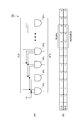
図1は、第1実施形態のクロックデータ復元装置1の構成を示す図である。図2は、クロックデータ復元装置1が備えるクロック生成装置1Aの構成を示す図である。クロックデータ復元装置1は、入力信号(Data In)に基づいて復元クロック(RecoveredClock)および復元データ(Recovered Data)を生成するものであって、クロック生成装置1A、エッジ検出部50、極性検出部60、論理反転部70およびデータ出力部80を備える。クロック生成装置1Aは、信号選択部10、位相検出部13、位相制御部14、選択部15、位相遅延部20、時間測定部30および位相選択部40を含む。
(First embodiment)
FIG. 1 is a diagram illustrating a configuration of a clock
信号選択部10は、位相選択部40から出力される帰還クロック(FeedbackClock)、論理反転部70から出力されるエッジ信号(Edge)、および、エッジ検出部50から出力されるエッジ検出信号(Edge Detect)を入力する。エッジ信号は、入力信号(Data In)及び帰還クロック(Feedback Clock)に基づいて生成されるものであって、入力信号と同じビットレートを有し、このビットレートに応じたタイミングでエッジを有する。エッジ検出信号は、エッジ信号のエッジのタイミングを含む一定期間に亘って有意レベルとなる信号である。
The
信号選択部10は、エッジ検出信号が有意レベルであるときに、エッジ信号を選択して位相遅延部20へ出力する。すなわち、エッジ検出信号が有意レベルであるとき、論理反転部70から出力されるエッジ信号は信号選択部10を経て位相遅延部20に入力される。
The
一方、信号選択部10は、エッジ検出信号が非有意レベルであるときに、帰還クロックを論理反転した信号を選択して位相遅延部20へ出力する。すなわち、エッジ検出信号が非有意レベルであるとき、信号選択部10および位相選択部40は、帰還ループを構成しており、リングオシレータのように動作をして、位相遅延部20における遅延時間に応じた周波数でクロック発振をする。
On the other hand, when the edge detection signal is at an insignificant level, the
位相遅延部20は、縦続接続された複数個(P個)の遅延素子211〜21Pを含む。位相遅延部20は、信号選択部10から出力される信号を遅延素子211〜21Pのうちの初段の遅延素子211に入力する。位相遅延部20は、遅延素子211〜21Pそれぞれから各々の位置に応じた遅延量の信号を、時間測定部30および位相選択部40へ出力する。遅延素子211〜21Pそれぞれの遅延時間は一定であってよい。
The
時間測定部30は、位相遅延部20の遅延素子211〜21Pそれぞれから出力される信号のレベルに基づいて、エッジ信号の或るエッジのタイミングから1ビット相当時間経過時のエッジのタイミングまでのユニットインターバル時間を測定する。時間測定部30は、時間測定結果をデジタル値として出力することができるTime-to-Digital Converter(TDC)を構成する。時間測定部30は、フリップフロップ311〜31P、測定許可部32、AND回路35および例えばバブルエラー訂正部33を含む。
Based on the level of the signal output from each of the delay elements 21 1 to 21 P of the
フリップフロップ311〜31Pは、遅延素子211〜21Pそれぞれから出力される信号のデータを所定タイミングでラッチするラッチ部を構成する。すなわち、P個のフリップフロップ311〜31Pのうちの第pのフリップフロップ31pは、対応する遅延素子21pから出力される信号のデータを、信号選択部10から出力される信号(Edge In)のエッジのタイミングであって且つ測定許可部32が許可するタイミングでラッチする。測定許可部32は、信号選択部10から出力される信号(Edge In)を入力するとともに、エッジ検出部50から出力されるエッジ検出信号(EdgeDetect)を入力して、フリップフロップ311〜31Pによるラッチ動作の許否を判断して、そのラッチ動作を許可するときに有意レベルとなる信号(En)を出力する。AND回路35は、測定許可部32から出力される信号(En)が有意レベルであるときに、信号選択部10から出力される信号(Edge In)をフリップフロップ311〜31Pに与える。
The flip-flops 31 1 to 31 P constitute a latch unit that latches data of signals output from the delay elements 21 1 to 21 P at a predetermined timing. That is, of the P flip-flops 31 1 to 31 P , the p-th flip-flop 31 p converts the data of the signal output from the corresponding delay element 21 p to the signal (Edge Latching is performed at the timing of the edge of In) and the timing permitted by the
バブルエラー訂正部33は、フリップフロップ311〜31Pによりラッチされて出力されるPビットのデジタルデータのバブル対策の為に設けられており、このPビットのデジタルデータに対してバブルエラー訂正を行う。時間測定部30は、バブルエラー訂正部33から出力されるPビットのデジタルデータを、ユニットインターバル時間測定結果として選択部15を介して位相選択部40へ出力する。
The bubble
位相検出部13は、エッジ信号(Edge)と帰還クロック(Feedback Clock)との間の位相関係を検出する。位相検出部13は、エッジ信号および帰還クロックのうち何れの位相が進んでいるかを検出し、また、その位相差の大きさを検出する。なお、エッジ信号と帰還クロックとはレベルが互いに逆であるので、位相検出部13は何れか一方のレベルを反転させた後に両者の位相関係を検出する。位相検出部13は、図示されるように信号選択部10に入力されるエッジ信号を入力してもよいし、信号選択部10によりエッジ信号(Edge)が選択されて出力される信号(Edge In)を入力してもよい。位相検出部13は、信号選択部10から出力される信号(Edge In)を入力する場合には、信号選択部10における遅延と同等の遅延を与えられた帰還クロックを入力するのが好適である。
The
位相制御部14は、位相検出部13により検出される位相差が小さくなるように位相選択部40による信号選択動作を制御するための制御信号を生成し、選択部15を介してこの制御信号を位相選択部40へ出力する。
The
選択部15は、時間測定部30のバブルエラー訂正部33から出力されるユニットインターバル時間測定結果を表すPビットのデジタルデータ、および、位相制御部14から出力される制御信号のうち、何れか一方を選択して位相選択部40へ与える。選択部15は、エッジ検出信号(Edge Detect)に基づいて状態を判断して、後述するプリアンブルの期間では時間測定部30から出力されるPビットのデジタルデータを選択して位相選択部40へ与え、その後の通常データの期間では位相制御部14から出力される制御信号を選択して位相選択部40へ与える。
The
位相選択部40は、位相遅延部20の遅延素子211〜21Pのうち、時間測定部30により測定されたユニットインターバル時間に対応する位置、または、位相制御部14から出力される制御信号が指示する位置にある遅延素子から出力される信号を選択して、この信号を帰還クロック(Feedback Clock)として信号選択部10および極性検出部60へ出力する。また、位相選択部40は、位相遅延部20の遅延素子211〜21Pのうちの何れかの遅延素子から出力される信号を選択して、この信号をエッジ信号のビットレートに対応する周波数の復元クロック(Recovered Clock)としてデータ出力部80へ出力する。これら復元クロックおよび帰還クロックは、共に入力信号に基づいて復元されたクロックであり、周波数が互いに同じであるが、位相が互いに異なっている。
The
エッジ検出部50は、入力信号(Data In)を入力し、この入力信号に遅延を付与した遅延入力信号(Delayed Data)を生成して、この遅延入力信号を論理反転部70およびデータ出力部80へ出力する。また、エッジ検出部50は、遅延入力信号のエッジのタイミングを含む一定期間に亘って有意レベルとなるエッジ検出信号(Edge Detect)を生成して、このエッジ検出信号を信号選択部10および測定許可部32へ出力する。エッジ検出部50は、縦続接続された遅延素子51〜53およびXOR回路54を含む。遅延素子51〜53それぞれの遅延時間Dは一定であるのが好ましい。
The
XOR回路54は、入力信号を遅延素子51により遅延時間Dだけ遅延させた信号と、入力信号を遅延素子51〜53により遅延時間3Dだけ遅延させた信号とを入力して、これら2つの信号の排他的論理和を表す信号をエッジ検出信号として出力する。また、エッジ検出部50は、入力信号を遅延素子51,52により遅延時間2Dだけ遅延させた信号を遅延入力信号として出力する。
The
極性検出部60は、入力信号(Data In)を入力するとともに、位相選択部40から出力される帰還クロック(Feedback Clock)を入力する。そして、極性検出部60は、これらの信号に基づいて論理反転指示信号(INV)を生成して、この論理反転指示信号を論理反転部70へ出力する。論理反転指示信号は、エッジ検出信号(Edge Detect)が有意レベルである期間に帰還クロック(FeedbackClock)および遅延入力信号Delayed Data)それぞれのエッジの極性が互いに同じであるときに有意レベルとなる。極性検出部60は、フリップフロップ61,62およびセレクタ63を含む。
The
一方のフリップフロップ61は、入力信号の立下りエッジのタイミングで、帰還クロックのレベルをラッチする。他方のフリップフロップ62は、入力信号の立上りエッジのタイミングで、帰還クロックのレベルを反転したレベルをラッチする。セレクタ63は、入力信号がローレベルであるときには、フリップフロップ61から出力される信号(X)を論理反転指示信号として出力し、入力信号がハイレベルであるときには、フリップフロップ62から出力される信号(Y)を論理反転指示信号として出力する。
One flip-
論理反転部70は、エッジ検出部50から出力される遅延入力信号(DelayedData)を入力するとともに、極性検出部60から出力される論理反転指示信号(INV)を入力する。論理反転部70は、論理反転指示信号が有意レベルであるときに、遅延入力信号を論理反転した信号をエッジ信号としてクロック生成装置へ出力する。一方、論理反転部70は、論理反転指示信号が非有意レベルであるときに、遅延入力信号をエッジ信号としてクロック生成装置へ出力する。
The
データ出力部80は、位相選択部40から出力される復元クロック(RecoveredClock)を入力するとともに、エッジ検出部50から出力される遅延入力信号(Delayed Data)を入力する。そして、データ出力部80は、復元クロックが指示するタイミングで遅延入力信号のデータをサンプリングしホールドして復元データ(Recovered Data)として出力する。データ出力部80は、フリップフロップ81,82を含む。フリップフロップ81は、復元クロックの立下りエッジのタイミングで遅延入力信号のデータをサンプリングしホールドして出力する。フリップフロップ82は、復元クロックの立上りエッジのタイミングで遅延入力信号のデータをサンプリングしホールドして出力する。
The
図3は、時間測定部30の測定許可部32の回路構成例を示す図である。測定許可部32は、フリップフロップ311〜31Pによるラッチ動作のタイミングを指示する信号(TDC Clk)を作り出す信号(En)を出力するものであって、INV回路321、フリップフロップ322,323、AND回路324、遅延素子326,327、EXNOR回路328およびOR回路329を含む。同図には、AND回路35も示されている。
FIG. 3 is a diagram illustrating a circuit configuration example of the
フリップフロップ322は、エッジ検出信号(Edge Detect)の立上りエッジのタイミングで、信号選択部10から出力される信号(Edge In)がINV回路321により論理反転された信号(x)をラッチする。フリップフロップ323は、エッジ検出信号(Edge Detect)の立上りエッジのタイミングで、フリップフロップ323から出力される信号(c)をラッチする。フリップフロップ322,323は、OR回路329から出力される信号(Reset)がローレベルであるときに初期化される。
The flip-
AND回路324は、フリップフロップ322から出力される信号(c)を論理反転した信号と、フリップフロップ323から出力される信号(d)とを入力して、これら2つの信号の論理積を表す信号(En)を出力する。AND回路35は、AND回路324から出力される信号(En)と信号選択部10から出力される信号(Edge In)との論理積を表す信号(TDC Clk)を出力する。
The AND
EXNOR回路328は、復元クロック(Recovered Clock)と、この復元クロックが遅延素子326により遅延された信号とを入力し、これら2つの信号の排他的論理和の反転を表す信号(a)を出力する。OR回路329は、EXNOR回路328から出力される信号(a)と、復元クロックが遅延素子327により遅延された信号とを入力し、これらの論理和を表す信号(Reset)をフリップフロップ322,323へ出力する。
The
図4は、時間測定部30の測定許可部32における各信号のタイミングチャートである。測定許可部32は、信号選択部10から出力される信号(Edge In)における立上りエッジ(レベル0→1の遷移)および立下りエッジ(レベル1→0の遷移)を見つけて、フリップフロップ311〜31Pによるラッチ動作のタイミングを指示する信号(TDC Clk)を出力する。INV回路321およびフリップフロップ322,323は、信号(EdgeIn)を反転させた信号(x)をエッジ検出信号(Edge Detect)の立上りエッジのタイミングでラッチすることにより、信号(EdgeIn)のエッジの極性(立上り及び立下りの何れであるか)を確認する。
FIG. 4 is a timing chart of each signal in the
AND回路324およびAND回路35は、信号(c),(d)がそれぞれローレベル、ハイレベルになったときのみ信号(En)信号をハイレベルとし、信号(Edge In)を信号(TDC Clk)として出力する。遅延素子326,327、EXNOR回路328およびOR回路329は、帰還クロック(Feedback)とエッジ検出信号(Edge Detect)とを組み合わせて、エッジの間隔が1ユニットインターバル時間を超えるときにフリップフロップ322,323をリセットすることにより、立上りエッジと立下りエッジとが1ユニットインターバル時間の間隔で来たときのみ、フリップフロップ311〜31Pによるラッチ動作を指示する。
The AND
図5は、時間測定部30のバブルエラー訂正部33の説明図である。バブルエラー訂正部33は、フリップフロップ311〜31Pによりラッチされて出力されるPビットのデジタルデータのメタスタビリティ対策の為に設けられており、このPビットのデジタルデータに対してバブルエラー訂正を行って、[11・・1100・・00]のように値1から値0への遷移が一つのみになるようにする。
FIG. 5 is an explanatory diagram of the bubble
同図(a)に回路構成が示されるように、バブルエラー訂正部33は、各々3入力のP個のAND回路341〜34Pを含む。AND回路341は、遅延素子211から出力される信号を入力して、そのまま出力する。AND回路342は、遅延素子211,212それぞれから出力される信号を入力して、これら2つの信号の論理積を表す信号を出力する。P個のAND回路341〜34PのうちAND回路341,342を除く各AND回路34pは、遅延素子21p−2,21p−1,21pそれぞれから出力される信号を入力して、これら3つの信号の論理積を表す信号を出力する。
As the circuit arrangement in FIG. (A) is shown, bubble
同図(b)に入出力信号の例が示されるように、バブルエラー訂正部33は、例えば、フリップフロップ311〜31Pから出力されるPビットのデジタルデータ[・・11101000・・]を入力したときに、これをPビットのデジタルデータ[・・11100000・・]に変換して出力する。
As shown in the example of the input / output signal in FIG. 5B, the bubble
図6は、位相選択部40の回路構成例を示す図である。位相選択部40は、帰還クロックを選択して出力するための帰還クロック選択回路と、復元クロックを選択して出力するための復元クロック選択回路とを含む。帰還クロック選択回路と復元クロック選択回路とは互いに同一の構成であってよい。同図では、P=128として、帰還クロック選択回路が示されている。
FIG. 6 is a diagram illustrating a circuit configuration example of the
帰還クロック選択回路は、128個のINV回路411〜41128、128個のスイッチ421〜42128、8個のINV回路431〜438、および、8個のスイッチ441〜448を含む。8組のINV回路41およびスイッチ42に対して1組のINV回路43およびスイッチ44の割合で設けられている。 The feedback clock selection circuit includes 128 INV circuits 41 1 to 41 128 , 128 switches 42 1 to 42 128 , 8 INV circuits 43 1 to 43 8 , and 8 switches 44 1 to 44 8 . Including. One set of INV circuit 43 and switch 44 is provided for eight sets of INV circuit 41 and switch 42.
各INV回路41pは、対応する遅延素子21pから出力される信号を入力して、それを論理反転した信号を、対応するスイッチ42pへ出力する。各スイッチ42pは、閉じているときに、対応するINV回路41pから出力される信号を、8個のINV回路431〜438のうちの何れかのINV回路43p1へ入力させる。各INV回路43p1は、入力した信号を論理反転した信号を、対応するスイッチ44p1へ出力する。各スイッチ44p1は、閉じているときに、対応するINV回路43p1から出力される信号を帰還クロックとして出力する。
Each INV circuit 41 p receives a signal output from the corresponding delay element 21 p, and outputs a signal obtained by logically inverting it to the corresponding switch 42 p . Each switch 42 p, when closed, a signal output from the corresponding INV circuit 41 p, it is input to one of the INV circuit 43 p1 of the eight
帰還クロック選択回路は、位相遅延部20の遅延素子211〜21Pのうちユニットインターバル時間に対応する位置にある遅延素子に対応するスイッチ42pを閉じ、このスイッチ42pの後段にあるスイッチ44p1を閉じ、その他のスイッチを開くことで、ユニットインターバル時間に対応する位置にある遅延素子から出力される信号を選択して、この信号を帰還クロックとして出力することができる。
The feedback clock selection circuit closes the switch 42 p corresponding to the delay element in the position corresponding to the unit interval time among the delay elements 21 1 to 21 P of the
図7は、エッジ検出部50における各信号のタイミングチャートである。遅延入力信号(Delayed Data)は、入力信号(Data In)に対して時間2Dだけ遅延した信号である。エッジ検出信号は、遅延入力信号の各エッジのタイミングを中心として時間2Dの期間に亘って有意レベルとなる。
FIG. 7 is a timing chart of each signal in the
図8は、極性検出部60および論理反転部70における各信号のタイミングチャートである。同図には、入力信号(Data In)、遅延入力信号(Delayed Data)、帰還クロック(Feedback Clock)、極性検出部60のフリップフロップ61から出力される信号(X)、極性検出部60のフリップフロップ62から出力される信号(Y)、および、極性検出部60のセレクタ63から出力される論理反転指示信号(INV)、それぞれが示されている。同図に示されるように、帰還クロックおよび遅延入力信号それぞれのエッジの極性が互いに同じであると、論理反転指示信号は有意レベルとなる。
FIG. 8 is a timing chart of each signal in the
図9は、論理反転部70および信号選択部10における各信号のタイミングチャートである。同図には、エッジ検出信号(Edge Detect)、遅延入力信号(Delayed Data)、帰還クロック(Feedback Clock)、論理反転指示信号(INV)、論理反転部70から出力されて信号選択部10に入力されるエッジ信号(Edge)、および、信号選択部10から出力される信号(Edge In)、それぞれが示されている。同図に示されるように、エッジ検出信号が有意レベルである期間(遅延入力信号のエッジのタイミングを含む一定期間)に、エッジ信号および帰還クロックそれぞれのエッジの極性は互いに逆になり、信号選択部10から出力される信号(Edge In)は帰還クロックを論理反転したものと同じとなって、クロック発振が維持される。
FIG. 9 is a timing chart of each signal in the
図10は、データ出力部80における各信号のタイミングチャートである。同図には、遅延入力信号(Delayed Data)、帰還クロック(Feedback Clock)、復元クロック(Recovered Clock)、フリップフロップ81から出力される復元データ(RecoveredData1)、および、フリップフロップ82から出力される復元データ(Recovered Data2)、それぞれが示されている。同図に示されるように、帰還クロックおよび復元クロックは、周波数が互いに同じであるが、位相が互いに異なっている。帰還クロックおよび復元クロックの周波数は、遅延入力信号のビットレート(すなわち、入力信号のビットレート)の2分の1となっている。復元クロックの位相(すなわち、復元クロックのエッジのタイミング)は、データ出力部80による遅延入力信号のデータのサンプリング誤りが無いように設定される。帰還クロックおよび復元クロックそれぞれの位相の差は例えばπ/2である。
FIG. 10 is a timing chart of each signal in the
次に、クロック生成装置1Aについて更に詳細に説明する。図11は、クロック生成装置1Aの位相遅延部20および時間測定部30における各信号のタイミングチャートである。同図は、信号選択部10から出力される信号(Edge In)として[010]の3ビットのデータが入力された場合に位相遅延部20の遅延素子211〜21Pおよび時間測定部30のフリップフロップ311〜31Pそれぞれから出力される信号のタイミングチャートを示す。
Next, the
例えば、論理反転指示信号(INV)が非有意レベルであり、入力信号として3ビットデータ[010]が入力されるとき、遅延入力信号(Delayed Data)は、立上りエッジを有し、また、この立上りエッジからユニットインターバル時間が経過した時点で立下りエッジを有する。エッジ検出信号(Edge Detect)は、遅延入力信号のこれら2つのエッジそれぞれのタイミングを含む一定期間に亘って有意レベルとなる。したがって、エッジ信号(Edge)として遅延入力信号と同じ3ビットデータ[010]が信号選択部10により選択されて位相遅延部20に入力される。
For example, when the logical inversion instruction signal (INV) is at a non-significant level and 3-bit data [010] is input as an input signal, the delayed input signal (Delayed Data) has a rising edge, and this rising edge It has a falling edge when the unit interval time elapses from the edge. The edge detection signal (Edge Detect) becomes a significant level over a certain period including the timing of each of these two edges of the delayed input signal. Therefore, the same 3-bit data [010] as the delayed input signal is selected as the edge signal (Edge) by the
信号選択部10から出力される信号(Edge In)の立上りエッジのタイミングを基準時刻とし、各遅延素子21nの遅延時間をτとする。このとき、基準時刻から時間mτ(ただし、ユニットインターバル時間より短い時間)が経過した時点では、遅延素子211〜21Pのうち初段から第m段までの遅延素子211〜21mそれぞれから出力される信号はハイレベルであって、これより後段の遅延素子21m−1〜21Pそれぞれから出力される信号はローレベルである。
The timing of the rising edge of the signal (Edge In) output from the
基準時刻からユニットインターバル時間が経過した時点(すなわち、信号選択部10から出力される信号(Edge In)の立下りエッジのタイミング)において、遅延素子211〜21Pのうち初段から第m段までの遅延素子211〜21mそれぞれから出力される信号がハイレベルであって、これより後段の遅延素子21m−1〜21Pそれぞれから出力される信号がローレベルであれば、ユニットインターバル時間はmτ以上(m+1)τ未満であることが判る。 From the first stage to the m-th stage among the delay elements 21 1 to 21 P at the time when the unit interval time has elapsed from the reference time (that is, the timing of the falling edge of the signal (Edge In) output from the signal selection unit 10) If the signal output from each of the delay elements 21 1 to 21 m is at the high level and the signal output from each of the delay elements 21 m−1 to 21 P at the subsequent stage is at the low level, the unit interval time Is greater than or equal to mτ and less than (m + 1) τ.
信号選択部10から出力される信号(Edge In)の立下りエッジのタイミングで、各フリップフロップ31pが、対応する遅延素子21pから出力される信号のデータをラッチする。すると、フリップフロップ311〜31Pのうち初段から第m段までのフリップフロップ311〜31mそれぞれから出力される信号はハイレベルであって、これより後段のフリップフロップ31m−1〜31Pそれぞれから出力される信号はローレベルである。 At the timing of the falling edge of the signal output from the signal selection section 10 (Edge In), each flip-flop 31 p is, latches the data signal output from the corresponding delay elements 21 p. Then, among the flip-flops 31 1 to 31 P , the signals output from the flip-flops 31 1 to 31 m from the first stage to the m-th stage are at a high level, and the flip-flops 31 m−1 to 31 in the subsequent stage are thereafter. The signal output from each P is at a low level.
P個のフリップフロップ311〜31Pによりラッチされて出力されるPビットのデジタルデータは、第1ビットから第pビットまでが値1であって、残りの(P−p)ビットが値0となって、[11・・1100・・00]のようになる。時間測定部30は、このPビットのデジタルデータからユニットインターバル時間を求める。そして、位相選択部40は、P個の遅延素子211〜21Pのうちユニットインターバル時間に対応する位置にある遅延素子から出力される信号を選択して帰還クロック(Feedback Clock)として出力するとともに、復元クロック(RecoveredClock)をも出力する。
P-bit digital data latched and output by P flip-flops 31 1 to 31 P has a
図12は、第1実施形態のクロックデータ復元装置1の動作シーケンスを示す図である。同図には、クロックデータ復元装置1に入力される入力信号(Data In)の波形、クロックデータ復元装置1の状態、および、クロックデータ復元装置1の消費電力、が示されている。同図に示されるように、入力信号(Data In)が入力される動作期間と、信号入力が無い待機期間と、が交互に存在する。入力信号は、通常データ(Normal data)と、この通常データの前に付加されるプリアンブル(Preamble)と、通常データの後に付加されるストップデータ(Stop Data)とを含む。
FIG. 12 is a diagram illustrating an operation sequence of the clock
信号入力が無い待機期間では、入力信号は値0のままであり、クロックデータ復元装置1はパワーダウンモードであって消費電力が殆どない。待機期間が終了すると先ず入力信号のプリアンブルのデータとして[10]が入力される。これにより、クロックデータ復元装置1は、前述したようにしてプリアンブルのデータのユニットインターバル時間に対応した周波数の復元クロック(Recovered Clock)および帰還クロック(Feedback Clock)の発振が得られ、クロックおよびデータを復元することができるロック(Lock)状態になる。そして、プリアンブルに続いて入力される通常データに基づいて復元クロックおよび復元データが得られる。通常データの後に付加されるストップデータは、例えば一定ビット数以上の値1が連続するデータである。このストップデータが入力されると、クロックデータ復元装置1は、動作期間が終了して待機期間となったことを認識して、パワーダウンモードとなって消費電力が殆どなくなる。
In the standby period in which there is no signal input, the input signal remains at
図13は、第1実施形態のクロックデータ復元装置1における各信号のタイミングチャートである。同図には、入力信号(Data In)、論理反転指示信号(INV)、遅延入力信号(Delayed Data)、エッジ検出信号(Edge Detect)、エッジ信号(Edge)、帰還クロック(Feedback Clock)、復元クロック(Recovered Clock)、ラッチ動作のタイミングを指示する信号(TDC Clk)、および、時間測定部30により測定され位相選択部40に与えられるユニットインターバル時間を表す信号(Phase Select)、が示されている。また、同図には、入力信号としてプリアンブルおよび通常データが入力される期間が示されている。
FIG. 13 is a timing chart of each signal in the clock
クロックデータ復元装置1は、プリアンブルの2ビットデータ[10]が入力されることでロック状態となり、プリアンブルに続く通常データに基づいて復元クロックおよび復元データを得ることができる。図9を用いて説明したとおり、入力信号にエッジがあったとき、クロックデータ復元装置1は、そのエッジを位相遅延部20に入力させることにより、復元クロック(Recovered Clock)の位相を入力信号の位相に合わせることができる。
The clock
また、クロックデータ復元装置1は、通常データ(Normal Data)送信時、信号選択部10から出力される信号(Edge In)に3ビットデータ[010]が存在するときに、時間測定部30によりユニットインターバル時間を測定して、この測定したユニットインターバル時間に基づいてクロック発振の周波数を調整することができる。これにより、動作中に温度・電圧などの変動により位相遅延部20の各遅延素子の特性が変わったり、入力信号のビットレートがゆっくり変動したりしても、正常にクロックおよびデータの復元動作をすることができる。
In addition, the clock
ところで、以上までに説明した動作例では、帰還クロック(Feedback Clock)および復元クロック(Recovered Clock)それぞれの周波数は、位相遅延部20のP個の遅延素子211〜21Pのうち位相選択部40により選択される遅延素子の位置により決定されるので、離散的な複数の値から選ばれる一つの値でしかない。それ故、これらのクロックの周波数と入力信号のビットレートとが互いに一致しない場合があり、その結果、CID耐性が悪い場合がある。本実施形態のクロック生成装置1Aは、このような問題に対処するために位相検出部13および位相制御部14を備えている。
By the way, in the operation examples described above, the frequency of each of the feedback clock (Feedback Clock) and the recovered clock (Recovered Clock) is the
位相検出部13は、エッジ信号(Edge)と帰還クロック(Feedback Clock)との間の位相関係を検出する。位相制御部14は、位相検出部13により検出される位相差が小さくなるように位相選択部40による信号選択動作を制御するための制御信号を生成し、この制御信号を位相選択部40へ与える。これにより、位相選択部40において、位相遅延部20のP個の遅延素子211〜21Pのうち第Nの遅延素子21Nと第(N+1)の遅延素子21N+1とが或る比率(1−α):αで選択されて、実効的に第(N+α)の遅延素子が選択されることに等しくなる。なお、Nは整数であり、αは0以上1以下の小数である。
The
図14は、位相制御部14の構成例を示す図である。位相制御部14は、累積加算器(Accumulator)141、ラッチ部142および加算器143を含むΔΣ変調器の構成を有する。これらの要素は帰還クロック(Feedback Clock)に同期して動作する。なお、ここでは、これらの要素は3ビットのデータを扱うものとする。累積加算器141は、ラッチ部142によりラッチされて出力される3ビットデータを入力するとともに、αを表す3ビットデータを入力して、これら入力した2つの3ビットデータを加算する。そして、累積加算器141は、その加算結果のうち下位3ビットデータをラッチ部142へ出力し、また、その加算の際にオーバーフローが生じた場合には値1を加算器143へ出力する。ラッチ部142は、累積加算器141から出力される3ビットデータを入力してラッチする。
FIG. 14 is a diagram illustrating a configuration example of the
加算器143は、値Nを表すデータを入力するとともに、累積加算器141での加算の際にオーバーフローが生じた場合には値1を表すデータを入力する。累積加算器141での加算の際にオーバーフローが生じる確率はαである。したがって、加算器143から出力されるデータは、確率(1−α)で値Nを表し、確率αで値(N+1)を表すことになる。例えば、α=0.25であるすると、累積加算器141での加算の際にオーバーフローが生じるのは、4回のうち1回の割合である。したがって、加算器143から出力されるデータは、4回のうち3回の割合で値Nを表し、4回のうち1回の割合で値(N+1)を表すことになる。
The
位相制御部14は、加算器143から出力されるデータに基づいて、位相選択部40による信号選択動作を制御するための制御信号を生成し、この制御信号を位相選択部40へ与える。これにより、位相選択部40において、位相遅延部20のP個の遅延素子211〜21Pのうち第Nの遅延素子21Nと第(N+1)の遅延素子21N+1とが比率(1−α):αで選択されて、実効的に第(N+α)の遅延素子が選択されることに等しくなる。
The
なお、位相制御部14の構成は、図14に示されたものに限られることはなく、他の態様も可能である。位相制御部14は、フィルタを含む構成であってもよいし、ΔΣ変調器およびフィルタを含む構成であってもよい。また、フィルタは、ローパスフィルタおよび累積加算器の双方または何れか一方を含む構成であってもよい。
Note that the configuration of the
図15は、位相制御部14におけるα決定方法等の一例を説明するフローチャートである。まず、プリアンブルのデータに基づいて時間測定部30によりユニットインターバル時間が測定され、その測定されたユニットインターバル時間に基づいて位相遅延部20のP個の遅延素子211〜21Pのうち第Nの遅延素子21Nが位相選択部40により選択される(ステップS11)。これによりロック状態となり、プリアンブルに続く通常データに基づいて復元クロックおよび復元データが得られる。
FIG. 15 is a flowchart for explaining an example of an α determination method and the like in the
入力信号にエッジが現れると(ステップS12)、エッジ信号(Edge)と帰還クロック(FeedbackClock)との間の位相関係が位相検出部13により検出され、エッジ信号より帰還クロックの位相が遅ければ(ステップS13でYes)、Nから値1が減算されて新たなNとされる(ステップS14)。エッジ信号より帰還クロックの位相が速く(ステップS15でYes)、位相差が閾値より大きければ(ステップS16でYes)、Nに値1が加算されて新たなNとされる(ステップS17)。Nが更新された後、ステップS12に戻る(ステップS18)。ステップS12〜S18の繰り返し処理は、例えばプリアンブルに重畳するジッタ等の影響でロック直後のNが適切でない場合に、このNを最適化するものである。
When an edge appears in the input signal (step S12), the phase relationship between the edge signal (Edge) and the feedback clock (FeedbackClock) is detected by the
エッジ信号より帰還クロックの位相が速く(ステップS15でNo)、位相差が閾値以下であれば(ステップS16でNo)、ステップS21以降の処理に進み、αを決定する。まず、初期値としてα=0.5とする(ステップS21)。入力信号にエッジが現れると(ステップS22)、エッジ信号(Edge)と帰還クロック(FeedbackClock)との間の位相関係が位相検出部13により検出され、エッジ信号より帰還クロックの位相が遅ければ(ステップS23でYes)、αから値0.125が減算されて新たなαとされる(ステップS24)。エッジ信号より帰還クロックの位相が速ければ(ステップS25でYes)、αに値0.125が加算されて新たなαとされる(ステップS26)。αが更新された後、ステップS22に戻る(ステップS27)。このようにしてαが決定される。この決定されたαが、図14に示された位相制御部14の累積加算器141に入力される。
If the phase of the feedback clock is faster than the edge signal (No in step S15) and the phase difference is equal to or smaller than the threshold (No in step S16), the process proceeds to step S21 and subsequent steps to determine α. First, α = 0.5 is set as an initial value (step S21). When an edge appears in the input signal (step S22), the phase relationship between the edge signal (Edge) and the feedback clock (FeedbackClock) is detected by the
以上のとおり、第1実施形態のクロックデータ復元装置1およびクロック生成装置1Aは、PLLが不要であり、また、参照クロックを生成するための回路も不要であるので、回路規模を小さくすることができ、製造コストを低くすることができる。また、本実施形態のクロックデータ復元装置1およびクロック生成装置1Aは、信号入力が無い待機期間の消費電力を低減することができる。また、本実施形態のクロックデータ復元装置1は、信号入力開始後に短時間でクロックおよびデータの復元を開始することができる。更に、本実施形態では、クロック周波数は、離散的な複数の値から選ばれる一つの値(選択される遅延素子21Nの位置Nに応じた周波数)に限られることなく、実効的にNとN+1との間の値に応じた周波数とすることができるので、CID耐性を改善することができる。
As described above, the clock
(第2実施形態)
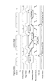
図16は、第2実施形態のクロックデータ復元装置2の構成を示す図である。図1に示された第1実施形態のクロックデータ復元装置1の構成と比較すると、第2実施形態のクロックデータ復元装置2は、エッジ検出部50、極性検出部60、論理反転部70およびデータ出力部80を備える点で同じであるが、クロック生成装置1Aに替えてクロック生成装置2Aを備える点で相違する。クロック生成装置2Aは、第1実施形態と同様の信号選択部10、位相検出部13および位相制御部14、帰還クロックの位相を粗調整する位相粗調整部11、ならびに、帰還クロックの位相を微調整する位相微調整部12、を備える。
(Second Embodiment)
FIG. 16 is a diagram illustrating a configuration of the clock
図17は、位相粗調整部11の構成を示す図である。位相粗調整部11は、位相遅延部201、時間測定部301および位相選択部401を含む。位相遅延部201は、第1実施形態における位相遅延部20と同様に、縦続接続された複数個(Q個)の遅延素子211,1〜211,Qを含む。そのうち初段の遅延素子211,1は、信号選択部10から出力される信号(Edge In)を入力する。時間測定部301は、第1実施形態における時間測定部30と同様に、位相遅延部201の遅延素子211,1〜211,Qそれぞれから出力される信号のレベルに基づいてユニットインターバル時間を測定する。位相選択部401は、第1実施形態における位相選択部40と同様に、位相遅延部201の遅延素子211,1〜211,Qのうち時間測定部301により測定されたユニットインターバル時間に対応する位置にある遅延素子から出力される信号を選択して帰還クロック(Feedback Clock 1)として位相微調整部12へ出力する。
FIG. 17 is a diagram illustrating a configuration of the phase
図18は、位相微調整部12の構成を示す図である。位相微調整部12は、位相遅延部202、時間測定部302、位相選択部402および選択部15を含む。位相遅延部202は、第1実施形態における位相遅延部20と同様に、縦続接続された複数個(R個)の遅延素子212,1〜212,Rを含む。そのうち初段の遅延素子212,1は、位相粗調整部11の位相選択部401から出力される帰還クロック(Feedback Clock 1)を入力する。時間測定部302は、第1実施形態における時間測定部30と同様に、位相遅延部202の遅延素子212,1〜212,Rそれぞれから出力される信号のレベルに基づいてユニットインターバル時間を測定する。位相選択部402は、第1実施形態における位相選択部40と同様に、位相遅延部202の遅延素子212,1〜212,Rのうち時間測定部302により測定されたユニットインターバル時間に対応する位置にある遅延素子から出力される信号を選択して帰還クロック(Feedback Clock)として信号選択部10および極性検出部60へ出力する。選択部15は、時間測定部302から出力されるユニットインターバル時間測定結果を表すRビットのデジタルデータ、および、位相制御部14から出力される制御信号のうち、何れか一方を選択して位相選択部402へ与える。
FIG. 18 is a diagram illustrating a configuration of the phase
信号選択部10は、位相微調整部12の位相選択部402から出力される帰還クロックを入力する。位相粗調整部11の位相遅延部201は、信号選択部10から出力される信号を初段の遅延素子211,1に入力する。位相微調整部12の位相遅延部202は、位相粗調整部11の位相選択部401から出力される帰還クロックを初段の遅延素子212,1に入力する。これにより帰還クロックについての帰還ルートが構成される。
帰還クロックの周期は、位相粗調整部11の位相遅延部201で粗調整された遅延時間と、位相微調整部12の位相遅延部202で微調整された遅延時間と、の和に応じたものとなる。位相粗調整部11の位相遅延部201の各遅延素子の遅延時間は、位相微調整部12の位相遅延部202の各遅延素子の遅延時間より長い。これにより、位相粗調整部11は帰還クロックの位相を粗調整し、位相微調整部12は帰還クロックの位相を微調整することができる。位相粗調整部11の位相遅延部201における遅延時間はユニットインターバル時間より僅かに短く(数個の遅延素子の遅延時間分だけ短く)設定されて、これらの差が位相微調整部12の位相遅延部202における遅延時間として微調整されてもよい。
Cycle of the feedback clock, corresponding to the phase delay unit and 20 1 in the coarse adjustment delay time, the delay time which is finely adjusted by the
位相粗調整部11の位相選択部401は、位相遅延部201の遅延素子211,1〜211,Qのうちの何れかの遅延素子から出力される信号を選択して、この信号をエッジ信号のビットレートに対応する周波数の復元クロック(Recovered Clock)としてデータ出力部80へ出力する。
図19は、位相粗調整部11の位相遅延部201の各遅延素子211,qの回路構成例を示す図である。図20は、位相微調整部12の位相遅延部202の各遅延素子212,rの回路構成例を示す図である。これらの図では、各遅延素子が差動信号を入出力するものとして回路構成が示されている。
Figure 19 is a diagram showing a circuit configuration example of the delay elements 21 1, q the
図19に示される位相粗調整部11の位相遅延部201の各遅延素子211,qは、差動信号を入力する2つの入力端子INP,INN、差動信号を出力する2つの出力端子OUTP,OUTN、および、INV回路211〜214を含む。INV回路211は、入力端子INPに入力された信号を論理反転して出力端子OUTNへ出力する。INV回路212は、入力端子INNに入力された信号を論理反転して出力端子OUTPへ出力する。INV回路213の入力端は出力端子OUTPと接続され、INV回路213の出力端は出力端子OUTNと接続されている。INV回路214の入力端は出力端子OUTNと接続され、INV回路214の出力端は出力端子OUTPと接続されている。図20に示される位相微調整部12の位相遅延部202は、図19に示される単位回路が縦続接続されていて、これらの単位回路の入出力端子を結ぶ抵抗器列が設けられて構成される。
Each delay element 21 1 of the
例えば、位相粗調整部11の各遅延素子211,qの遅延時間を約35psとすることができ、位相微調整部12の各遅延素子212,rの遅延時間を約6psとすることができる。また、位相粗調整部11の遅延素子の個数Qを18とすることができ、位相微調整部12の遅延素子の個数Rを12とすることができる。
For example, the delay time of each delay element 21 1, q of the phase
図21は、第2実施形態のクロックデータ復元装置2における各信号のタイミングチャートである。同図には、入力信号(Data In)、遅延入力信号(Delayed Data)、エッジ信号(Edge)、位相微調整部12の位相選択部402から出力される帰還クロック(Feedback Clock)、復元クロック(Recovered Clock)、位相粗調整部11の時間測定部301のラッチ動作のタイミングを指示する信号(Coarse TDC Clk)、位相粗調整部11の時間測定部301により測定され位相選択部401に与えられるユニットインターバル時間を表す信号(Coarse Phase Select)、位相微調整部12の時間測定部302のラッチ動作のタイミングを指示する信号(Fine TDC Clk)、および、位相微調整部12の時間測定部302により測定され位相選択部402に与えられるユニットインターバル時間を表す信号(Fine Phase Select)、が示されている。また、同図には、入力信号としてプリアンブルおよび通常データが入力される期間が示されている。
FIG. 21 is a timing chart of each signal in the clock
クロックデータ復元装置2は、プリアンブルの4ビットデータ[1010]が入力されることでロック状態となり、プリアンブルに続く通常データに基づいて復元クロックおよび復元データを得ることができる。このとき、プリアンブルの第1の立下りエッジにより位相粗調整部11の位相遅延部201の遅延量が設定され、プリアンブルの第2の立下りエッジにより位相微調整部12の位相遅延部202の遅延量が設定される。入力信号にエッジがあったとき、クロックデータ復元装置2は、そのエッジを位相遅延部201,202に入力させることにより、復元クロック(Recovered Clock)の位相を入力信号の位相に合わせることができる。
The clock
また、クロックデータ復元装置2は、通常データ(Normal Data)に3ビットデータ[010]が存在するときに、時間測定部301,302によりユニットインターバル時間を測定して、この測定したユニットインターバル時間に基づいてクロック発振の周波数を調整することができる。これにより、動作中に温度・電圧などの変動により位相遅延部201,202の各遅延素子の特性が変わったり、入力信号のビットレートがゆっくり変動したりしても、正常にクロックおよびデータの復元動作をすることができる。
The clock
なお、位相制御部14は、位相選択部401,402のうち何れの信号選択動作を制御してもよいが、位相粗調整部11の位相選択部401より位相微調整部12の位相選択部402の信号選択動作を制御するのが好適である。位相微調整部12の位相選択部402の信号選択動作を制御することで、より精細にクロック周波数を調整することができる。
The
以上のとおり、第2実施形態のクロックデータ復元装置2およびクロック生成装置2Aも、PLLが不要であり、また、参照クロックを生成するための回路も不要であるので、回路規模を小さくすることができ、製造コストを低くすることができる。また、本実施形態のクロックデータ復元装置2およびクロック生成装置2Aも、信号入力が無い待機期間の消費電力を低減することができる。また、本実施形態のクロックデータ復元装置2は、信号入力開始後に短時間でクロックおよびデータの復元を開始することができる。更に、本実施形態でも、クロック周波数は、離散的な複数の値から選ばれる一つの値(選択される遅延素子212,Nの位置Nに応じた周波数)に限られることなく、実効的にNとN+1との間の値に応じた周波数とすることができるので、CID耐性を改善することができる。
As described above, the clock
第2実施形態のクロック生成装置2Aは、第1実施形態のクロック生成装置1Aと比較して、以下のような利点を有する。
The
第1実施形態のクロック生成装置1Aでは、エッジ検出信号(Edge Detect)が非有意レベルであるときにリングオシレータのように動作をするので、位相遅延部20において帰還クロックが受ける全遅延時間は入力信号(Data In)のユニットインターバル時間と等しいことが望ましい。それを実現するには、位相遅延部20の各遅延素子21での遅延量は小さいことが望ましい。それ故、位相遅延部20の遅延素子21の個数Pは大きくなりがちである。例えば、動作周波数を2分の1にすると、位相遅延部20の遅延素子21の個数Pは2倍になり、時間測定部30のフリップフロップ31の個数Pも2倍になる。また、動作周波数を4分の1にすると、位相遅延部20の遅延素子21の個数Pは4倍になり、時間測定部30のフリップフロップ31の個数Pも4倍になる。このように、第1実施形態のクロック生成装置1Aは、リングオシレータのように動作する際のクロック発振周波数を精確に設定しようとすると、回路面積が大きくなるだけでなく、消費電力も大きくなって、動作周波数のワイドレンジ化に限界がある。
In the
これに対して、第2実施形態のクロック生成装置2Aでは、位相遅延部201,時間測定部301および位相選択部401を含む位相粗調整部11において遅延時間を入力信号(Data In)のユニットインターバル時間と粗く等しくなるように設定する一方で、位相遅延部202,時間測定部302および位相選択部402を含む位相微調整部12において遅延量を微調整することができる。したがって、第2実施形態のクロック生成装置2Aでは、位相遅延部201,202の遅延素子の個数(Q+R)および時間測定部301,302のフリップフロップの個数(Q+R)の増大を回避することができて、回路面積の増大および消費電力の増大を回避しつつ、クロック発振周波数の精確さと動作周波数のワイドレンジ化とを両立させることができる。
In contrast, in the
なお、以上までに説明した第2実施形態では位相粗調整部11(位相遅延部201,時間測定部301,位相選択部401)と位相微調整部12(位相遅延部202,時間測定部302,位相選択部402)とからなる2段の構成であったが、3段以上の構成であってもよい。3段以上の構成とする場合、位相制御部14は、何れの段の位相選択部の信号選択動作を制御してもよいが、最も精細に遅延を設定することができる段の位相選択部の信号選択動作を制御するのが好適である。
In the second embodiment described above, the phase coarse adjustment unit 11 (
(他の実施形態)
本発明は、上記実施形態に限定されるものではなく、種々の変形が可能である。例えば、位相遅延部20,201,202それぞれにおいて、図22(a)に示されるように縦続接続された複数の遅延素子の遅延時間は一定であってもよいし、同図(b)に示されるように縦続接続された複数の遅延素子のうち後段のものほど遅延時間が長くなっていているのも好ましい。後者の場合、各遅延素子の遅延時間が、その位置に対して対数関数的に長くなるように設定されているのが好ましい。動作周波数が遅いほど多くの遅延素子を使い且つ精度が荒くてよいので、後段ほど遅延時間を長くすれば、位相遅延部20の遅延素子の個数および時間測定部30のフリップフロップの個数の増大を回避することができて、回路面積の増大および消費電力の増大を回避しつつ、クロック発振周波数の精確さと動作周波数のワイドレンジ化とを両立させることができる。
(Other embodiments)
The present invention is not limited to the above embodiment, and various modifications can be made. For example, the
また、本発明は、図23に示されるような実施形態も可能である。図23は、他の実施形態のクロックデータ復元装置3の構成を示す図である。図16に示された第2実施形態の構成と比較すると、図23に示される実施形態のクロックデータ復元装置3は、入力信号位相検出部91および入力信号位相調整部92を更に備える点で相違する。
Further, the present invention can be implemented as shown in FIG. FIG. 23 is a diagram illustrating a configuration of the clock
入力信号位相検出部91は、帰還クロック(Feedback Clock)と遅延入力信号(Delayed Data)との間の位相関係を検出する。入力信号位相検出部91は、例えば、帰還クロック、および、この帰還クロックに対して位相が一定量ずつ異なる複数のクロック、それぞれにより、遅延入力信号をラッチして、そのラッチにより得られた3以上のデータのレベルに基づいて、帰還クロックと遅延入力信号との間の位相関係を検出することができる。入力信号位相調整部92は、入力信号位相検出部91による検出結果に基づいて、データ出力部80に入力される遅延入力信号(Delayed Data)の位相を調整する。
The input
このような構成とすることで、データ出力部80に入力される遅延入力信号(Delayed Data)と帰還クロック(Feedback Clock)との間の位相関係を最適化することができ、また、データ出力部80に入力される遅延入力信号(Delayed Data)と復元クロック(Recovered Clock)との間の位相関係を最適化することができる。したがって、データ出力部80において、遅延入力信号(Delayed Data)の各ビットのデータの中心時刻に復元クロック(RecoveredClock)のエッジが存在するようにすることができる。これによって、ジッタ耐性やCID耐性を改善することができる。
With such a configuration, the phase relationship between the delayed input signal (Delayed Data) input to the
なお、図1および図2に示された第1実施形態の構成においても入力信号位相検出部91および入力信号位相調整部92が設けられてもよい。
Note that the input
1〜3…クロックデータ復元装置、1A,2A…クロック生成装置、10…信号選択部、11…位相粗調整部、12…位相微調整部、13…位相検出部、14…位相制御部、15…選択部、20,201,202…位相遅延部、211〜21P,211,1〜211,Q,212,1〜212,R…遅延素子、30,301,302…時間測定部、311〜31P…フリップフロップ、32…測定許可部、33…バブルエラー訂正部、40,401,402…位相選択部、50…エッジ検出部、51〜53…遅延素子、54…XOR回路、60…極性検出部、61,62…フリップフロップ、63…セレクタ、70…論理反転部、80…データ出力部、81,82…フリップフロップ、91…入力信号位相検出部、92…入力信号位相調整部。 DESCRIPTION OF SYMBOLS 1-3 ... Clock data decompression | restoration apparatus, 1A, 2A ... Clock generation apparatus, 10 ... Signal selection part, 11 ... Phase coarse adjustment part, 12 ... Phase fine adjustment part, 13 ... Phase detection part, 14 ... Phase control part, 15 ... selection unit, 20, 20 1 , 20 2 ... phase delay unit, 21 1 to 21 P , 21 1 , 1 to 21 1, Q , 21 2 , 1 to 21 2, R ... delay element, 30, 30 1 , 30 2 ... time measuring unit, 31 1 to 31 P ... flip-flop, 32 ... measurement permission unit, 33 ... bubble error correction unit, 40, 40 1 , 40 2 ... phase selection unit, 50 ... edge detection unit, 51 to 53 ... Delay element, 54 ... XOR circuit, 60 ... Polarity detection unit, 61, 62 ... Flip-flop, 63 ... Selector, 70 ... Logic inversion unit, 80 ... Data output unit, 81, 82 ... Flip-flop, 91 ... Input signal phase Detection unit, 92 ... input No. phase adjustment unit.
Claims (5)
縦続接続された複数個の遅延素子を含み、前記信号選択部から出力される信号を前記複数個の遅延素子のうちの初段の遅延素子に入力し、前記複数個の遅延素子それぞれから各々の位置に応じた遅延量の信号を出力する位相遅延部と、
前記複数個の遅延素子それぞれから出力される信号のレベルに基づいて、前記エッジ信号の或るエッジのタイミングから1ビット相当時間経過時のエッジのタイミングまでのユニットインターバル時間を測定する時間測定部と、
前記複数個の遅延素子のうち前記時間測定部により測定された前記ユニットインターバル時間に対応する位置にある遅延素子から出力される信号を選択して前記帰還クロックとして出力するとともに、前記複数個の遅延素子のうちの何れかの遅延素子から出力される信号を選択して前記エッジ信号のビットレートに対応する周波数のクロックとして出力する位相選択部と、
前記エッジ信号と前記帰還クロックとの間の位相関係を検出する位相検出部と、
前記位相検出部により検出される位相差が小さくなるように前記位相選択部による信号選択動作を制御する位相制御部と、
を備えるクロック生成装置。 An edge signal having an edge at a timing according to a feedback clock, a bit rate, and an edge detection signal that becomes a significant level over a certain period including the edge timing of the edge signal are input, and the edge detection signal is at a significant level. A signal selection unit that selects and outputs the edge signal when it is, and selects and outputs a signal obtained by logically inverting the feedback clock when the edge detection signal is at a non-significant level;
A plurality of delay elements connected in cascade; a signal output from the signal selection unit is input to a first-stage delay element among the plurality of delay elements; A phase delay unit that outputs a signal with a delay amount according to
A time measuring unit for measuring a unit interval time from a certain edge timing of the edge signal to an edge timing when a time corresponding to 1 bit elapses based on a level of a signal output from each of the plurality of delay elements; ,
Among the plurality of delay elements, a signal output from a delay element at a position corresponding to the unit interval time measured by the time measuring unit is selected and output as the feedback clock, and the plurality of delays A phase selector that selects a signal output from any one of the delay elements and outputs it as a clock having a frequency corresponding to the bit rate of the edge signal;
A phase detector that detects a phase relationship between the edge signal and the feedback clock;
A phase control unit that controls a signal selection operation by the phase selection unit so that a phase difference detected by the phase detection unit is small;
A clock generator comprising:
各位相遅延部Dnが、縦続接続された複数個の遅延素子を含み、
各位相遅延部Dnの各遅延素子の遅延時間と、他の位相遅延部Dn1の各遅延素子の遅延時間とが、互いに異なり、
各時間測定部Mnが、位相遅延部Dnの複数個の遅延素子それぞれから出力される信号のレベルに基づいて前記ユニットインターバル時間を測定し、
各位相選択部Snが、位相遅延部Dnの複数個の遅延素子のうち時間測定部Mnにより測定された前記ユニットインターバル時間に対応する位置にある遅延素子から出力される信号を選択して前記帰還クロックとして出力し、
前記信号選択部が、位相選択部SNから出力される前記帰還クロックを入力し、
位相遅延部D1が、前記信号選択部から出力される信号を初段の遅延素子に入力し、
位相遅延部D1〜DNのうち位相遅延部D1を除く各位相遅延部Dnが、位相選択部Sn−1から出力される前記帰還クロックを初段の遅延素子に入力し、
位相選択部S1〜SNのうちの何れかの位相選択部Snが、位相遅延部Dnの複数個の遅延素子のうちの何れかの遅延素子から出力される信号を選択して前記クロックとして出力し、
前記位相制御部が、位相選択部S1〜SNのうちの何れかによる信号選択動作を制御する、
請求項1に記載のクロック生成装置(ただし、Nは2以上の整数、n,n1は1以上N以下の整数)。 Phase delay units D 1 to DN as the phase delay units, time measurement units M 1 to M N as the time measurement units, and phase selection units S 1 to S N as the phase selection units,
Each phase delay unit D n comprises a plurality of delay elements connected in cascade,
The delay time of each delay element of each phase delay unit D n is different from the delay time of each delay element of the other phase delay unit D n1 ,
Each time measurement unit M n measures the unit interval time based on the level of the signal output from each of the plurality of delay elements of the phase delay unit D n ,
Each phase selection unit S n selects a signal output from a delay element at a position corresponding to the unit interval time measured by the time measurement unit M n among the plurality of delay elements of the phase delay unit D n. Output as the feedback clock,
The signal selection unit inputs the feedback clock output from the phase selection unit SN ,
A phase delay unit D 1, receives the signal outputted from the signal selector to the delay element of the initial stage,
Each phase delay unit D n excluding the phase delay unit D 1 of the phase delay unit D 1 to D N are inputs the feedback clock output from the phase selecting unit S n-1 to the first-stage delay element,
Any one of the phase selectors S n of the phase selectors S 1 to S N selects a signal output from any one of the plurality of delay elements of the phase delay unit D n , and Output as a clock,
The phase control unit controls a signal selection operation by any of the phase selection units S 1 to S N ;
The clock generation device according to claim 1, wherein N is an integer of 2 or more, and n and n1 are integers of 1 to N.
請求項1〜3の何れか1項に記載のクロック生成装置と、
前記入力信号に遅延を付与した遅延入力信号を生成して出力するともに、前記遅延入力信号のエッジのタイミングを含む一定期間に亘って有意レベルとなるエッジ検出信号を生成して前記クロック生成装置へ出力するエッジ検出部と、
前記エッジ検出信号が有意レベルである期間に前記帰還クロックおよび前記遅延入力信号それぞれのエッジの極性が互いに同じであるときに有意レベルとなる論理反転指示信号を生成して出力する極性検出部と、
前記論理反転指示信号が有意レベルであるときに前記遅延入力信号を論理反転した信号を前記エッジ信号として前記クロック生成装置へ出力し、前記論理反転指示信号が非有意レベルであるときに前記遅延入力信号を前記エッジ信号として前記クロック生成装置へ出力する論理反転部と、
前記クロック生成装置から出力される前記クロックが指示するタイミングで前記遅延入力信号のデータをサンプリングしホールドして出力するデータ出力部と、
を備え、
前記クロック生成装置から出力される前記クロックを前記入力信号に基づく復元クロックとして出力し、前記データ出力部から出力されるデータを前記入力信号に基づく復元データとして出力する、
クロックデータ復元装置。 An apparatus for recovering a clock and data based on an input signal,
The clock generation device according to any one of claims 1 to 3,
A delayed input signal obtained by adding a delay to the input signal is generated and output, and an edge detection signal that becomes a significant level over a certain period including the timing of the edge of the delayed input signal is generated to the clock generating device. An edge detector to output;
A polarity detection unit that generates and outputs a logic inversion instruction signal that becomes a significant level when the edges of the feedback clock and the delayed input signal have the same polarity during a period in which the edge detection signal is at a significant level;
When the logic inversion instruction signal is at a significant level, a signal obtained by logically inverting the delay input signal is output to the clock generator as the edge signal, and when the logic inversion instruction signal is at an insignificant level, the delay input A logic inversion unit for outputting a signal to the clock generation device as the edge signal;
A data output unit that samples and holds the data of the delayed input signal at a timing indicated by the clock output from the clock generation device; and
With
Outputting the clock output from the clock generation device as a recovered clock based on the input signal, and outputting data output from the data output unit as recovered data based on the input signal;
Clock data recovery device.
前記入力信号位相検出部による検出結果に基づいて前記データ出力部に入力される前記遅延入力信号の位相を調整する入力信号位相調整部と、
を更に備える請求項4に記載のクロックデータ復元装置。
An input signal phase detector for detecting a phase relationship between the feedback clock and the delayed input signal;
An input signal phase adjustment unit that adjusts the phase of the delayed input signal input to the data output unit based on a detection result by the input signal phase detection unit;
The clock data restoration device according to claim 4, further comprising:
Priority Applications (2)
| Application Number | Priority Date | Filing Date | Title |
|---|---|---|---|
| JP2016009903A JP6604859B2 (en) | 2016-01-21 | 2016-01-21 | Clock generation device and clock data restoration device |
| US15/408,631 US9887830B2 (en) | 2016-01-21 | 2017-01-18 | Clock generating apparatus and clock data recovering apparatus |
Applications Claiming Priority (1)
| Application Number | Priority Date | Filing Date | Title |
|---|---|---|---|
| JP2016009903A JP6604859B2 (en) | 2016-01-21 | 2016-01-21 | Clock generation device and clock data restoration device |
Publications (2)
| Publication Number | Publication Date |
|---|---|
| JP2017130838A true JP2017130838A (en) | 2017-07-27 |
| JP6604859B2 JP6604859B2 (en) | 2019-11-13 |
Family
ID=59359685
Family Applications (1)
| Application Number | Title | Priority Date | Filing Date |
|---|---|---|---|
| JP2016009903A Active JP6604859B2 (en) | 2016-01-21 | 2016-01-21 | Clock generation device and clock data restoration device |
Country Status (2)
| Country | Link |
|---|---|
| US (1) | US9887830B2 (en) |
| JP (1) | JP6604859B2 (en) |
Families Citing this family (9)
| Publication number | Priority date | Publication date | Assignee | Title |
|---|---|---|---|---|
| US10305495B2 (en) * | 2016-10-06 | 2019-05-28 | Analog Devices, Inc. | Phase control of clock signal based on feedback |
| CN108333910B (en) * | 2018-05-02 | 2019-12-31 | 晶晨半导体(上海)股份有限公司 | A New Time-to-Digital Converter |
| CN112422295B (en) * | 2019-08-23 | 2023-06-13 | 微芯片技术股份有限公司 | Ethernet interface and related systems, methods and devices |
| CN112415323B (en) | 2019-08-23 | 2024-07-09 | 微芯片技术股份有限公司 | Diagnosing cable faults within a network |
| CN112422385B (en) | 2019-08-23 | 2022-11-29 | 微芯片技术股份有限公司 | Interface for improved media access and related systems, methods and devices |
| CN112422153B (en) | 2019-08-23 | 2023-04-07 | 微芯片技术股份有限公司 | Method and system for processing data reception after detecting collisions at a shared transmission medium |
| US11513577B2 (en) | 2020-03-24 | 2022-11-29 | Microchip Technology Incorporated | Low connection count interface wake source communication according to 10SPE local and remote wake and related systems, methods, and devices |
| CN111654281B (en) * | 2020-06-10 | 2023-08-04 | 上海兆芯集成电路股份有限公司 | time converter |
| US12353240B2 (en) * | 2021-12-22 | 2025-07-08 | Intel Corporation | Selectable clock sources |
Citations (7)
| Publication number | Priority date | Publication date | Assignee | Title |
|---|---|---|---|---|
| JPH0677819A (en) * | 1992-03-02 | 1994-03-18 | Internatl Business Mach Corp <Ibm> | Phase restoration device of digital circuit |
| JP2000228660A (en) * | 1998-12-03 | 2000-08-15 | Mitsubishi Electric Corp | Clock regeneration / identification device |
| US20030012320A1 (en) * | 2001-07-11 | 2003-01-16 | Micron Technology, Inc | Delay locked loop fine tune |
| JP2007243735A (en) * | 2006-03-09 | 2007-09-20 | Elpida Memory Inc | Dll circuit and semiconductor device comprising the same |
| JP2009268047A (en) * | 2008-04-29 | 2009-11-12 | Renesas Technology Corp | Pll circuit |
| JP2011009922A (en) * | 2009-06-24 | 2011-01-13 | Elpida Memory Inc | DLL circuit and semiconductor device including the same |
| JP2014060520A (en) * | 2012-09-14 | 2014-04-03 | Thine Electronics Inc | Clock generating device and clock-data recovery device |
Family Cites Families (2)
| Publication number | Priority date | Publication date | Assignee | Title |
|---|---|---|---|---|
| US8149978B2 (en) * | 2007-03-12 | 2012-04-03 | Nippon Telegraph And Telephone Corporation | Clock/data recovery circuit |
| US8018261B2 (en) * | 2008-03-25 | 2011-09-13 | Micron Technology, Inc. | Clock generator and methods using closed loop duty cycle correction |
-
2016
- 2016-01-21 JP JP2016009903A patent/JP6604859B2/en active Active
-
2017
- 2017-01-18 US US15/408,631 patent/US9887830B2/en active Active
Patent Citations (7)
| Publication number | Priority date | Publication date | Assignee | Title |
|---|---|---|---|---|
| JPH0677819A (en) * | 1992-03-02 | 1994-03-18 | Internatl Business Mach Corp <Ibm> | Phase restoration device of digital circuit |
| JP2000228660A (en) * | 1998-12-03 | 2000-08-15 | Mitsubishi Electric Corp | Clock regeneration / identification device |
| US20030012320A1 (en) * | 2001-07-11 | 2003-01-16 | Micron Technology, Inc | Delay locked loop fine tune |
| JP2007243735A (en) * | 2006-03-09 | 2007-09-20 | Elpida Memory Inc | Dll circuit and semiconductor device comprising the same |
| JP2009268047A (en) * | 2008-04-29 | 2009-11-12 | Renesas Technology Corp | Pll circuit |
| JP2011009922A (en) * | 2009-06-24 | 2011-01-13 | Elpida Memory Inc | DLL circuit and semiconductor device including the same |
| JP2014060520A (en) * | 2012-09-14 | 2014-04-03 | Thine Electronics Inc | Clock generating device and clock-data recovery device |
Also Published As
| Publication number | Publication date |
|---|---|
| JP6604859B2 (en) | 2019-11-13 |
| US9887830B2 (en) | 2018-02-06 |
| US20170214513A1 (en) | 2017-07-27 |
Similar Documents
| Publication | Publication Date | Title |
|---|---|---|
| JP6604859B2 (en) | Clock generation device and clock data restoration device | |
| JP5948195B2 (en) | Clock generation device and clock data restoration device | |
| KR101632657B1 (en) | Time-to-digital convertoer and all-digital phase locked loop | |
| US7826583B2 (en) | Clock data recovery apparatus | |
| US9455667B2 (en) | Fractional-N all digital phase locked loop incorporating look ahead time to digital converter | |
| US8634509B2 (en) | Synchronized clock phase interpolator | |
| US8155256B2 (en) | Method and apparatus for asynchronous clock retiming | |
| EP1178609B1 (en) | Phase detector | |
| KR102577232B1 (en) | Hybrid clock data recovery circuit and receiver | |
| US20130271193A1 (en) | Circuits and methods to guarantee lock in delay locked loops and avoid harmonic locking | |
| JP2007110370A (en) | Digital phase detector | |
| US9455725B2 (en) | Phase detector and associated phase detecting method | |
| KR100839502B1 (en) | Thermometer code generator, output frequency control device of voltage controlled oscillator using thermometer code, frequency fixed loop using thermometer code generator | |
| JP4886276B2 (en) | Clock data recovery device | |
| JP3623948B2 (en) | Burst mode receiving apparatus resistant to noise and its clock signal and data recovery method | |
| CN110518906A (en) | Signal generating circuit and its method, digit time conversion circuit and its method | |
| WO2021036775A1 (en) | Signal generation circuit and method, and digital-to-time conversion circuit and method | |
| US20070230646A1 (en) | Phase recovery from forward clock | |
| JP2005252447A (en) | Lock detection circuit and method | |
| US7750711B2 (en) | Phase select circuit with reduced hysteresis effect | |
| US11711200B2 (en) | Multiphase clock generators with digital calibration | |
| KR20230089958A (en) | Clock data recovery circuit for display | |
| JP5747070B2 (en) | Phase-locked loop circuit and oscillation method |
Legal Events
| Date | Code | Title | Description |
|---|---|---|---|
| A80 | Written request to apply exceptions to lack of novelty of invention |
Free format text: JAPANESE INTERMEDIATE CODE: A80 Effective date: 20160208 |
|
| A621 | Written request for application examination |
Free format text: JAPANESE INTERMEDIATE CODE: A621 Effective date: 20181204 |
|
| A131 | Notification of reasons for refusal |
Free format text: JAPANESE INTERMEDIATE CODE: A131 Effective date: 20190820 |
|
| A977 | Report on retrieval |
Free format text: JAPANESE INTERMEDIATE CODE: A971007 Effective date: 20190821 |
|
| A521 | Request for written amendment filed |
Free format text: JAPANESE INTERMEDIATE CODE: A523 Effective date: 20190930 |
|
| TRDD | Decision of grant or rejection written | ||
| A01 | Written decision to grant a patent or to grant a registration (utility model) |
Free format text: JAPANESE INTERMEDIATE CODE: A01 Effective date: 20191008 |
|
| A61 | First payment of annual fees (during grant procedure) |
Free format text: JAPANESE INTERMEDIATE CODE: A61 Effective date: 20191015 |
|
| R150 | Certificate of patent or registration of utility model |
Ref document number: 6604859 Country of ref document: JP Free format text: JAPANESE INTERMEDIATE CODE: R150 |
|
| R250 | Receipt of annual fees |
Free format text: JAPANESE INTERMEDIATE CODE: R250 |
|
| R250 | Receipt of annual fees |
Free format text: JAPANESE INTERMEDIATE CODE: R250 |
|
| R250 | Receipt of annual fees |
Free format text: JAPANESE INTERMEDIATE CODE: R250 |
|
| R250 | Receipt of annual fees |
Free format text: JAPANESE INTERMEDIATE CODE: R250 |