JP2016028441A - Method for manufacturing semiconductor device - Google Patents
Method for manufacturing semiconductor device Download PDFInfo
- Publication number
- JP2016028441A JP2016028441A JP2015200300A JP2015200300A JP2016028441A JP 2016028441 A JP2016028441 A JP 2016028441A JP 2015200300 A JP2015200300 A JP 2015200300A JP 2015200300 A JP2015200300 A JP 2015200300A JP 2016028441 A JP2016028441 A JP 2016028441A
- Authority
- JP
- Japan
- Prior art keywords
- film
- oxide semiconductor
- semiconductor film
- transistor
- hard mask
- Prior art date
- Legal status (The legal status is an assumption and is not a legal conclusion. Google has not performed a legal analysis and makes no representation as to the accuracy of the status listed.)
- Withdrawn
Links
Images


Classifications
-
- H—ELECTRICITY
- H10—SEMICONDUCTOR DEVICES; ELECTRIC SOLID-STATE DEVICES NOT OTHERWISE PROVIDED FOR
- H10D—INORGANIC ELECTRIC SEMICONDUCTOR DEVICES
- H10D30/00—Field-effect transistors [FET]
- H10D30/60—Insulated-gate field-effect transistors [IGFET]
- H10D30/67—Thin-film transistors [TFT]
- H10D30/674—Thin-film transistors [TFT] characterised by the active materials
- H10D30/6755—Oxide semiconductors, e.g. zinc oxide, copper aluminium oxide or cadmium stannate
-
- H—ELECTRICITY
- H10—SEMICONDUCTOR DEVICES; ELECTRIC SOLID-STATE DEVICES NOT OTHERWISE PROVIDED FOR
- H10D—INORGANIC ELECTRIC SEMICONDUCTOR DEVICES
- H10D30/00—Field-effect transistors [FET]
- H10D30/60—Insulated-gate field-effect transistors [IGFET]
- H10D30/67—Thin-film transistors [TFT]
- H10D30/6729—Thin-film transistors [TFT] characterised by the electrodes
-
- H—ELECTRICITY
- H10—SEMICONDUCTOR DEVICES; ELECTRIC SOLID-STATE DEVICES NOT OTHERWISE PROVIDED FOR
- H10D—INORGANIC ELECTRIC SEMICONDUCTOR DEVICES
- H10D30/00—Field-effect transistors [FET]
- H10D30/60—Insulated-gate field-effect transistors [IGFET]
- H10D30/67—Thin-film transistors [TFT]
- H10D30/6757—Thin-film transistors [TFT] characterised by the structure of the channel, e.g. transverse or longitudinal shape or doping profile
-
- H—ELECTRICITY
- H10—SEMICONDUCTOR DEVICES; ELECTRIC SOLID-STATE DEVICES NOT OTHERWISE PROVIDED FOR
- H10D—INORGANIC ELECTRIC SEMICONDUCTOR DEVICES
- H10D64/00—Electrodes of devices having potential barriers
- H10D64/60—Electrodes characterised by their materials
- H10D64/62—Electrodes ohmically coupled to a semiconductor
-
- H—ELECTRICITY
- H10—SEMICONDUCTOR DEVICES; ELECTRIC SOLID-STATE DEVICES NOT OTHERWISE PROVIDED FOR
- H10D—INORGANIC ELECTRIC SEMICONDUCTOR DEVICES
- H10D86/00—Integrated devices formed in or on insulating or conducting substrates, e.g. formed in silicon-on-insulator [SOI] substrates or on stainless steel or glass substrates
- H10D86/01—Manufacture or treatment
- H10D86/021—Manufacture or treatment of multiple TFTs
- H10D86/0231—Manufacture or treatment of multiple TFTs using masks, e.g. half-tone masks
-
- H—ELECTRICITY
- H10—SEMICONDUCTOR DEVICES; ELECTRIC SOLID-STATE DEVICES NOT OTHERWISE PROVIDED FOR
- H10D—INORGANIC ELECTRIC SEMICONDUCTOR DEVICES
- H10D86/00—Integrated devices formed in or on insulating or conducting substrates, e.g. formed in silicon-on-insulator [SOI] substrates or on stainless steel or glass substrates
- H10D86/40—Integrated devices formed in or on insulating or conducting substrates, e.g. formed in silicon-on-insulator [SOI] substrates or on stainless steel or glass substrates characterised by multiple TFTs
- H10D86/421—Integrated devices formed in or on insulating or conducting substrates, e.g. formed in silicon-on-insulator [SOI] substrates or on stainless steel or glass substrates characterised by multiple TFTs having a particular composition, shape or crystalline structure of the active layer
- H10D86/423—Integrated devices formed in or on insulating or conducting substrates, e.g. formed in silicon-on-insulator [SOI] substrates or on stainless steel or glass substrates characterised by multiple TFTs having a particular composition, shape or crystalline structure of the active layer comprising semiconductor materials not belonging to the Group IV, e.g. InGaZnO
-
- H—ELECTRICITY
- H10—SEMICONDUCTOR DEVICES; ELECTRIC SOLID-STATE DEVICES NOT OTHERWISE PROVIDED FOR
- H10D—INORGANIC ELECTRIC SEMICONDUCTOR DEVICES
- H10D86/00—Integrated devices formed in or on insulating or conducting substrates, e.g. formed in silicon-on-insulator [SOI] substrates or on stainless steel or glass substrates
- H10D86/40—Integrated devices formed in or on insulating or conducting substrates, e.g. formed in silicon-on-insulator [SOI] substrates or on stainless steel or glass substrates characterised by multiple TFTs
- H10D86/60—Integrated devices formed in or on insulating or conducting substrates, e.g. formed in silicon-on-insulator [SOI] substrates or on stainless steel or glass substrates characterised by multiple TFTs wherein the TFTs are in active matrices
-
- H—ELECTRICITY
- H10—SEMICONDUCTOR DEVICES; ELECTRIC SOLID-STATE DEVICES NOT OTHERWISE PROVIDED FOR
- H10D—INORGANIC ELECTRIC SEMICONDUCTOR DEVICES
- H10D99/00—Subject matter not provided for in other groups of this subclass
Landscapes
- Thin Film Transistor (AREA)
- Metal-Oxide And Bipolar Metal-Oxide Semiconductor Integrated Circuits (AREA)
- Semiconductor Memories (AREA)
- Electrodes Of Semiconductors (AREA)
- Non-Volatile Memory (AREA)
- Engineering & Computer Science (AREA)
- Manufacturing & Machinery (AREA)
Abstract
【課題】高い電気特性を有する微細なトランジスタを歩留まりよく提供する。また、該トランジスタを含む半導体装置においても、高性能化、高信頼性化、および高生産化を達成する。【解決手段】酸化物半導体膜を微細加工する際に、ハードマスクを用いることで酸化物半導体膜の側面の凹凸を抑制することができる。具体的には、絶縁表面上の酸化物半導体膜と、酸化物半導体膜上の第1のハードマスクおよび第2のハードマスクと、酸化物半導体膜および第1のハードマスク上のソース電極と、酸化物半導体膜および第2のハードマスク上のドレイン電極と、ソース電極およびドレイン電極上のゲート絶縁膜と、ゲート絶縁膜と酸化物半導体膜と重畳するゲート電極と、を有し、第1のハードマスクおよび第2のハードマスクは、導電性を有する膜である。【選択図】図1A fine transistor having high electrical characteristics is provided with high yield. In a semiconductor device including the transistor, high performance, high reliability, and high production are achieved. When fine processing of an oxide semiconductor film is performed, unevenness on a side surface of the oxide semiconductor film can be suppressed by using a hard mask. Specifically, the oxide semiconductor film on the insulating surface, the first hard mask and the second hard mask on the oxide semiconductor film, the source electrode on the oxide semiconductor film and the first hard mask, A drain electrode overlying the oxide semiconductor film and the second hard mask; a gate insulating film over the source electrode and the drain electrode; and a gate electrode overlapping with the gate insulating film and the oxide semiconductor film; The hard mask and the second hard mask are conductive films. [Selection] Figure 1
Description
半導体装置およびその作製方法に関する。 The present invention relates to a semiconductor device and a manufacturing method thereof.
なお、本明細書中において半導体装置とは、半導体特性を利用することで機能しうる装
置全般を指し、電気光学装置、半導体回路および電子機器は全て半導体装置である。
Note that in this specification, a semiconductor device refers to all devices that can function by utilizing semiconductor characteristics, and an electro-optical device, a semiconductor circuit, and an electronic device are all semiconductor devices.
液晶表示装置や発光表示装置に代表されるフラットパネルディスプレイの多くに用いら
れているトランジスタは、ガラス基板上に形成されたアモルファスシリコン、単結晶シリ
コンまたは多結晶シリコンなどのシリコン半導体によって構成されている。また、該シリ
コン半導体を用いたトランジスタは、集積回路(IC)などにも利用されている。
Transistors used in many flat panel displays typified by liquid crystal display devices and light-emitting display devices are composed of silicon semiconductors such as amorphous silicon, single crystal silicon, or polycrystalline silicon formed on a glass substrate. . In addition, a transistor including the silicon semiconductor is used for an integrated circuit (IC) or the like.
近年、シリコン半導体に代わって、半導体特性を示す金属酸化物をトランジスタに用い
る技術が注目されている。なお、本明細書中では、半導体特性を示す金属酸化物を酸化物
半導体とよぶことにする。
In recent years, a technique using a metal oxide exhibiting semiconductor characteristics for a transistor instead of a silicon semiconductor has attracted attention. Note that in this specification, a metal oxide exhibiting semiconductor characteristics is referred to as an oxide semiconductor.
例えば、酸化物半導体として、酸化亜鉛、またはIn−Ga−Zn系酸化物を用いたト
ランジスタが開示されている(特許文献1参照)。
For example, a transistor using zinc oxide or an In—Ga—Zn-based oxide as an oxide semiconductor is disclosed (see Patent Document 1).
ところで、トランジスタの動作の高速化、トランジスタの低消費電力化、高集積化等を
達成するためにはトランジスタの微細化が必須である。
By the way, miniaturization of a transistor is indispensable in order to achieve high-speed operation of the transistor, low power consumption of the transistor, high integration, and the like.
しかし、トランジスタの微細化に伴って作製工程における歩留まりの低下が懸念される
。たとえば、チャネルとなる酸化物半導体膜を島状に微細加工する際に、酸化物半導体膜
の側面に凹凸が生じてしまうことによって酸化物半導体膜の形状のばらつきが大きくなり
、トランジスタの電気特性や信頼性にも影響を及ぼす可能性がある。
However, with the miniaturization of transistors, there is a concern about a decrease in yield in the manufacturing process. For example, when an oxide semiconductor film to be a channel is microfabricated into an island shape, unevenness is generated on the side surface of the oxide semiconductor film, resulting in a large variation in the shape of the oxide semiconductor film, and the electrical characteristics of the transistor Reliability may also be affected.
したがって、本発明の一態様は、微細な構造であっても高い電気特性を有するトランジ
スタなどを歩留まりよく提供することを目的の一とする。
Therefore, an object of one embodiment of the present invention is to provide a transistor or the like having high electrical characteristics even in a minute structure with high yield.
または、該トランジスタを含む半導体装置などにおいても、高性能化、高信頼性化、お
よび高生産化を達成することを目的の一とする。
Another object is to achieve high performance, high reliability, and high production even in a semiconductor device including the transistor.
本発明の一態様は、酸化物半導体膜を島状に微細加工する際に、ハードマスクを用いる
ことで酸化物半導体膜の側面の凹凸を抑制することができる。言い換えると、酸化物半導
体膜のラインエッジラフネス(Line Edge Roughness:LER)を低
減することができる。なお、「ラインエッジラフネス」とは、膜の側面の凸凹の程度をい
う。また、電子ビームまたは液浸露光等を用いてレジストを露光することで形成された、
線幅が小さいレジストマスクを用いることでチャネル長を短くすることができる。さらに
、ハードマスクの少なくとも一部に導電性のある材料を用い、該ハードマスクの一部をソ
ース電極およびドレイン電極の一部として機能させることができ、ソース電極およびドレ
イン電極の微細加工も該ハードマスクで行うことができる。具体的な構成および作製方法
は、以下の通りである。
In one embodiment of the present invention, when the oxide semiconductor film is microfabricated into an island shape, unevenness on the side surface of the oxide semiconductor film can be suppressed by using a hard mask. In other words, the line edge roughness (LER) of the oxide semiconductor film can be reduced. “Line edge roughness” means the degree of unevenness on the side surface of the film. Also, formed by exposing the resist using an electron beam or immersion exposure, etc.
By using a resist mask having a small line width, the channel length can be shortened. Furthermore, a conductive material is used for at least a part of the hard mask, and a part of the hard mask can function as a part of the source electrode and the drain electrode. Can be done with a mask. The specific configuration and manufacturing method are as follows.
本発明の一態様は、絶縁表面上の酸化物半導体膜と、酸化物半導体膜上の第1のハード
マスクおよび第2のハードマスクと、酸化物半導体膜および第1のハードマスク上のソー
ス電極と、酸化物半導体膜および第2のハードマスク上のドレイン電極と、ソース電極お
よびドレイン電極上のゲート絶縁膜と、ゲート絶縁膜と酸化物半導体膜と重畳するゲート
電極と、を有し、第1のハードマスクおよび第2のハードマスクは、導電性を有する膜で
あることを特徴とする半導体装置である。
One embodiment of the present invention includes an oxide semiconductor film over an insulating surface, a first hard mask and a second hard mask over the oxide semiconductor film, and a source electrode over the oxide semiconductor film and the first hard mask. A drain electrode on the oxide semiconductor film and the second hard mask, a gate insulating film on the source electrode and the drain electrode, and a gate electrode overlapping the gate insulating film and the oxide semiconductor film, The first hard mask and the second hard mask are semiconductor devices that are conductive films.
また、本発明の他の一態様は、絶縁表面上の酸化物半導体膜と、酸化物半導体膜上の第
1のハードマスクおよび第2のハードマスクと、酸化物半導体膜および第1のハードマス
ク上のソース電極と、酸化物半導体膜および第2のハードマスク上のドレイン電極と、ソ
ース電極およびドレイン電極上のゲート絶縁膜と、ゲート絶縁膜と酸化物半導体膜と重畳
するゲート電極と、を有し、第1のハードマスクおよび第2のハードマスクは、積層膜で
あり、積層膜の酸化物半導体膜と接する膜は、導電性を有する膜であることを特徴とする
半導体装置である。
Another embodiment of the present invention is an oxide semiconductor film over an insulating surface, a first hard mask and a second hard mask over the oxide semiconductor film, an oxide semiconductor film, and a first hard mask. An upper source electrode, an oxide semiconductor film and a drain electrode on the second hard mask, a gate insulating film on the source electrode and the drain electrode, and a gate electrode overlapping the gate insulating film and the oxide semiconductor film, In the semiconductor device, the first hard mask and the second hard mask are stacked films, and the film in contact with the oxide semiconductor film of the stacked film is a conductive film.
また、上記構成において、酸化物半導体膜を挟む第1の酸化物膜および第2の酸化物膜
を有し、第1の酸化物膜および第2の酸化物膜は、酸化物半導体膜よりも伝導帯下端のエ
ネルギーが0.05eV以上2eV以下の範囲で真空準位に近いことを特徴とする半導体
装置である。
In the above structure, the oxide semiconductor film includes the first oxide film and the second oxide film which sandwich the oxide semiconductor film, and the first oxide film and the second oxide film are more than the oxide semiconductor film. The semiconductor device is characterized in that the energy at the lower end of the conduction band is close to a vacuum level in a range of 0.05 eV to 2 eV.
また、上記構成において、酸化物半導体膜とソース電極との間、および酸化物半導体膜
と導電性を有する膜との間に設けられた第1の低抵抗領域と、酸化物半導体膜とドレイン
電極との間、および酸化物半導体膜と導電性を有する膜との間に設けられた第2の低抵抗
領域と、を有することを特徴とする半導体装置である。
In the above structure, the first low-resistance region provided between the oxide semiconductor film and the source electrode and between the oxide semiconductor film and the conductive film, the oxide semiconductor film, and the drain electrode And a second low resistance region provided between the oxide semiconductor film and the conductive film.
また、本発明の他の一態様は、絶縁表面上に第1の酸化物半導体膜を形成し、第1の酸
化物半導体膜上に第1のハードマスクを形成し、第1のハードマスク上に第1のレジスト
を形成し、露光を行い、第1のレジストマスクを形成し、第1のレジストマスクをマスク
として、第1のハードマスクをエッチングして第2のハードマスクを形成し、第1のレジ
ストマスクを除去し、第2のハードマスクをマスクとして、第1の酸化物半導体膜をエッ
チングして第2の酸化物半導体膜を形成し、絶縁表面、第2の酸化物半導体膜および第2
のハードマスク上にソース電極およびドレイン電極を形成し、第2のハードマスク、ソー
ス電極およびドレイン電極上に第2のレジストを形成し、露光を行い、第2のレジストマ
スクを形成し、第2のレジストマスクをマスクとして、第2のハードマスクをエッチング
して一対の第3のハードマスクを形成し、第2のレジストマスクを除去し、第2の酸化物
半導体膜、ソース電極、ドレイン電極および一対の第3のハードマスク上にゲート絶縁膜
を形成し、ゲート絶縁膜上に第2の酸化物半導体膜と重畳するゲート電極を形成すること
を特徴とする半導体装置の作製方法である。
According to another embodiment of the present invention, a first oxide semiconductor film is formed over an insulating surface, a first hard mask is formed over the first oxide semiconductor film, and the first hard mask is formed over the first hard mask. A first resist is formed on the substrate, exposure is performed, a first resist mask is formed, the first hard mask is etched using the first resist mask as a mask, and a second hard mask is formed. The first resist mask is removed, the second hard mask is used as a mask, the first oxide semiconductor film is etched to form a second oxide semiconductor film, an insulating surface, a second oxide semiconductor film, and Second
A source electrode and a drain electrode are formed on the second hard mask, a second resist is formed on the second hard mask, the source electrode, and the drain electrode, exposure is performed, a second resist mask is formed, and a second resist mask is formed. And the second hard mask is etched to form a pair of third hard masks, the second resist mask is removed, the second oxide semiconductor film, the source electrode, the drain electrode, and A method for manufacturing a semiconductor device is characterized in that a gate insulating film is formed over a pair of third hard masks, and a gate electrode overlapping with the second oxide semiconductor film is formed over the gate insulating film.
また、本発明の他の一態様は、絶縁表面上に第1の酸化物半導体膜を形成し、第1の酸
化物半導体膜上に第1のハードマスクを形成し、第1のハードマスク上に第1のレジスト
を形成し、露光を行い、第1のレジストマスクを形成し、第1のレジストマスクをマスク
として、第1のハードマスクをエッチングして第2のハードマスクを形成し、第1のレジ
ストマスクを除去し、第2のハードマスクをマスクとして、第1の酸化物半導体膜をエッ
チングして第2の酸化物半導体膜を形成し、絶縁表面、第2の酸化物半導体膜および第2
のハードマスク上に第2のレジストを形成し、露光を行い、第2のレジストマスクを形成
し、第2のレジストマスクをマスクとして、第2のハードマスクをエッチングして一対の
第3のハードマスクを形成し、第2のレジストマスクを除去し、絶縁表面、第2の酸化物
半導体膜および一対の第3のハードマスク上にソース電極およびドレイン電極を形成し、
第2の酸化物半導体膜、ソース電極、ドレイン電極および一対の第3のハードマスク上に
ゲート絶縁膜を形成し、ゲート絶縁膜上に第2の酸化物半導体膜と重畳するゲート電極を
形成することを特徴とする半導体装置の作製方法である。
According to another embodiment of the present invention, a first oxide semiconductor film is formed over an insulating surface, a first hard mask is formed over the first oxide semiconductor film, and the first hard mask is formed over the first hard mask. A first resist is formed on the substrate, exposure is performed, a first resist mask is formed, the first hard mask is etched using the first resist mask as a mask, and a second hard mask is formed. The first resist mask is removed, the second hard mask is used as a mask, the first oxide semiconductor film is etched to form a second oxide semiconductor film, an insulating surface, a second oxide semiconductor film, and Second
A second resist is formed on the hard mask, exposed to light, a second resist mask is formed, the second resist mask is used as a mask, and the second hard mask is etched to form a pair of third hard masks. Forming a mask, removing the second resist mask, forming a source electrode and a drain electrode over the insulating surface, the second oxide semiconductor film, and the pair of third hard masks;
A gate insulating film is formed over the second oxide semiconductor film, the source electrode, the drain electrode, and the pair of third hard masks, and a gate electrode overlapping with the second oxide semiconductor film is formed over the gate insulating film. This is a method for manufacturing a semiconductor device.
また、上記作製方法において、露光は、電子ビーム露光または液浸露光であることを特
徴とする半導体装置の作製方法である。
In the above manufacturing method, the exposure is electron beam exposure or liquid immersion exposure.
なお、本明細書等において、「ハードマスク」とは、レジスト材料以外の材料(金属材
料や絶縁材料)を用いて作製したマスクをいう。
Note that in this specification and the like, a “hard mask” refers to a mask manufactured using a material (metal material or insulating material) other than a resist material.
上記構成にすることで、微細な構造であっても高い電気特性を有するトランジスタを歩
留まりよく提供することができる。
With the above structure, a transistor having high electrical characteristics can be provided with high yield even when the structure is minute.
また、上記構成にすることで、該トランジスタを含む半導体装置においても、高性能化
、高信頼性化、および高生産化を達成することができる。
Further, with the above structure, high performance, high reliability, and high production can be achieved also in a semiconductor device including the transistor.
実施の形態について、図面を用いて詳細に説明する。但し、本発明は以下の説明に限定
されず、本発明の趣旨およびその範囲から逸脱することなくその形態および詳細を様々に
変更し得ることは当業者であれば容易に理解される。したがって、本発明は以下に示す実
施の形態の記載内容に限定して解釈されるものではない。なお、以下に説明する発明の構
成において、同一部分または同様な機能を有する部分には同一の符号を異なる図面間で共
通して用い、その繰り返しの説明は省略することがある。
Embodiments will be described in detail with reference to the drawings. However, the present invention is not limited to the following description, and it is easily understood by those skilled in the art that modes and details can be variously changed without departing from the spirit and scope of the present invention. Therefore, the present invention should not be construed as being limited to the description of the embodiments below. Note that in the structures of the invention described below, the same portions or portions having similar functions are denoted by the same reference numerals in different drawings, and description thereof is not repeated.
なお、トランジスタの「ソース」や「ドレイン」の機能は、異なる極性のトランジスタ
を採用する場合や、回路動作において電流の方向が変化する場合などには入れ替わること
がある。このため、本明細書等においては、「ソース」や「ドレイン」という用語は、入
れ替えて用いることができるものとする。
Note that the functions of the “source” and “drain” of the transistor may be interchanged when a transistor with a different polarity is used or when the direction of current changes during circuit operation. Therefore, in this specification and the like, the terms “source” and “drain” can be used interchangeably.
(実施の形態1)
本実施の形態では、本発明の一態様の半導体装置であるトランジスタについて図面を用
いて説明する。
(Embodiment 1)
In this embodiment, a transistor which is a semiconductor device of one embodiment of the present invention will be described with reference to drawings.
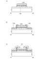
図1は、本発明の一態様のトランジスタ150の上面図および断面図である。図1(A
)は、上面図であり、図1(A)に示す一点鎖線A1−A2の断面が図1(B)に相当す
る。なお、図1(A)の上面図では、図の明瞭化のために一部の要素を省いて図示してい
る。
1A to 1C are a top view and cross-sectional views of a
) Is a top view, and a cross section taken along one-dot chain line A1-A2 shown in FIG. 1A corresponds to FIG. Note that in the top view of FIG. 1A, some elements are omitted for clarity.
図1に示すトランジスタ150は、基板100上の下地絶縁膜102と、下地絶縁膜1
02上の酸化物半導体膜104と、酸化物半導体膜104上のハードマスク106aおよ
びハードマスク106bと、ハードマスク106a上のハードマスク108aと、ハード
マスク106b上のハードマスク108bと、下地絶縁膜102、酸化物半導体膜104
、ハードマスク106aおよびハードマスク108a上のソース電極110aと、下地絶
縁膜102、酸化物半導体膜104、ハードマスク106bおよびハードマスク108b
上のドレイン電極110bと、酸化物半導体膜104、ハードマスク106a、ハードマ
スク106b、ハードマスク108a、ハードマスク108b、ソース電極110aおよ
びドレイン電極110b上のゲート絶縁膜112と、ゲート絶縁膜112上のゲート電極
114と、を有する。なお、ハードマスク106aおよびハードマスク106bは、導電
性を有する膜とする。また、酸化物半導体膜104の、ハードマスク106a、ハードマ
スク106b、ソース電極110aおよびドレイン電極110bと接する領域には、低抵
抗領域121aおよび低抵抗領域121bが形成される。また、ゲート絶縁膜112およ
びゲート電極114上に絶縁膜116が設けられていてもよい。絶縁膜116は必要に応
じて設ければよく、さらにその上部に他の絶縁膜を設けてもよい。
1 includes a
02, the
, The
The
基板100に大きな制限はない。例えば、ガラス基板、セラミック基板、石英基板、サ
ファイア基板などを、基板100として用いてもよい。また、シリコンや炭化シリコンな
どの単結晶半導体基板、多結晶半導体基板、シリコンゲルマニウムなどの化合物半導体基
板、SOI(Silicon On Insulator)基板などを適用することも可
能であり、これらの基板上に半導体素子が設けられたものを、基板100として用いても
よい。
There is no major limitation on the
また、基板100として、第5世代(1000mm×1200mmまたは1300mm
×1500mm)、第6世代(1500mm×1800mm)、第7世代(1870mm
×2200mm)、第8世代(2200mm×2500mm)、第9世代(2400mm
×2800mm)、第10世代(2880mm×3130mm)などの大型ガラス基板を
用いる場合、半導体装置の作製工程における熱処理などで生じる基板100の縮みによっ
て、微細な加工が困難になる場合ある。そのため、前述したような大型ガラス基板を基板
100として用いる場合、熱処理による縮みの小さいものを用いることが好ましい。例え
ば、基板100として、400℃、好ましくは450℃、さらに好ましくは500℃の温
度で1時間熱処理を行った後の縮み量が10ppm以下、好ましくは5ppm以下、さら
に好ましくは3ppm以下である大型ガラス基板を用いればよい。
Further, as the
× 1500mm), 6th generation (1500mm × 1800mm), 7th generation (1870mm)
× 2200mm), 8th generation (2200mm × 2500mm), 9th generation (2400mm)
When a large glass substrate such as × 2800 mm) or 10th generation (2880 mm × 3130 mm) is used, fine processing may be difficult due to shrinkage of the
また、基板100として、可とう性基板を用いてもよい。なお、可とう性基板上にトラ
ンジスタを設ける方法としては、非可とう性の基板上にトランジスタを作製した後、トラ
ンジスタを剥離し、可とう性基板である基板100に転置する方法もある。その場合には
、非可とう性基板とトランジスタとの間に剥離層を設けるとよい。
Further, a flexible substrate may be used as the
下地絶縁膜102は、基板100からの不純物の拡散を防止する役割を有するほか、熱
処理により、酸素を放出し、酸化物半導体膜に酸素を供給する役割を担うことができるた
め、酸素を含む絶縁膜であることが好ましく、過剰な酸素を含む絶縁膜がより好ましい。
また、上述のように基板100が他のデバイスが形成された基板である場合、下地絶縁膜
102は、層間絶縁膜としての機能も有する。その場合は、表面が平坦になるようにCM
P(Chemical Mechanical Polishing)法等で平坦化処理
を行うことが好ましい。
The base
In addition, when the
It is preferable to perform the flattening process by a P (Chemical Mechanical Polishing) method or the like.
下地絶縁膜102は、酸化シリコン膜、酸化ガリウム膜、酸化亜鉛膜、酸化アルミニウ
ム膜、ガリウム亜鉛酸化物膜、窒化シリコン膜、酸化窒化シリコン膜、酸化窒化アルミニ
ウム膜、または窒化酸化シリコン膜から選ばれた一層またはこれらの積層膜を用いること
ができる。
The base
ここで、熱処理によって酸素を放出する膜は、膜の表面温度が100℃以上700℃以
下、好ましくは100℃以上500℃以下の加熱処理で行われるTDS分析によって1×
1018atoms/cm3以上、1×1019atoms/cm3以上または1×10
20atoms/cm3以上の酸素(酸素原子数に換算)を放出することもある。
Here, a film which releases oxygen by heat treatment has a surface temperature of 100 ° C. or higher and 700 ° C. or lower, preferably 100 ° C. or higher and 500 ° C. or lower, and is 1 ×
10 18 atoms / cm 3 or more, 1 × 10 19 atoms / cm 3 or more, or 1 × 10
Oxygen (converted to the number of oxygen atoms) of 20 atoms / cm 3 or more may be released.
また、熱処理によって酸素を放出する膜は、過酸化ラジカルを含む。具体的には、過酸
化ラジカルに起因するスピン密度が、5×10¹⁷spins/cm3以上である。なお
、過酸化ラジカルを含む膜は、電子スピン共鳴(ESR:Electron Spin
Resonance)にて、g値が2.01近傍に非対称の信号を有することもある。
In addition, the film from which oxygen is released by heat treatment includes a peroxide radical. Specifically, the spin density resulting from the peroxide radical is 5 × 10 17 spins / cm 3 or more. Note that a film containing a peroxide radical is formed by an electron spin resonance (ESR).
Resonance) may have an asymmetric signal with a g value near 2.01.
また、過剰な酸素を含む絶縁膜は、酸素が過剰な酸化シリコン(SiOX(X>2))
であってもよい。酸素が過剰な酸化シリコン(SiOX(X>2))は、シリコン原子数
の2倍より多い酸素原子を単位体積当たりに含むものである。単位体積当たりのシリコン
原子数および酸素原子数は、ラザフォード後方散乱分光法(RBS:Rutherfor
d Backscattering Spectrometry)により測定した値であ
る。
An insulating film containing excess oxygen is formed using silicon oxide containing excess oxygen (SiO X (X> 2)).
It may be. Oxygen-excess silicon oxide (SiO X (X> 2)) contains oxygen atoms more than twice the number of silicon atoms per unit volume. The number of silicon atoms and oxygen atoms per unit volume is determined by Rutherford backscattering spectroscopy (RBS).
(d Backscattering Spectrometry).
酸化物半導体膜104は、少なくともインジウムを含む酸化物半導体膜である。例えば
、インジウムの他に亜鉛を含んでいてもよい。
The
以下では、酸化物半導体膜104のシリコン濃度について説明する。なお、トランジス
タの電気特性を安定にするためには、酸化物半導体膜104中の不純物濃度を低減し、酸
化物半導体膜104を真性または実質的に真性にすることが有効である。具体的には、酸
化物半導体膜のキャリア密度は、1×10¹⁷/cm3未満、1×1015/cm3未満
、または1×10¹³/cm3未満にするとよい。また、酸化物半導体膜において、主成
分以外(1原子%未満)の軽元素、半金属元素、金属元素などは不純物となる。例えば、
水素、窒素、炭素、シリコン、ゲルマニウムは、酸化物半導体膜中で不純物となる。
Hereinafter, the silicon concentration of the
Hydrogen, nitrogen, carbon, silicon, and germanium are impurities in the oxide semiconductor film.
また、酸化物半導体膜104中で水素および窒素は、ドナー準位を形成し、キャリア密
度を増大させてしまう。酸化物半導体膜104の水素濃度は二次イオン質量分析法(SI
MS:Secondary Ion Mass Spectrometry)において、
2×10²⁰atoms/cm3以下、好ましくは5×1019atoms/cm3以下
、より好ましくは1×10¹⁹atoms/cm3以下、さらに好ましくは5×1018
atoms/cm3以下とする。また、窒素濃度は、SIMSにおいて、5×1019a
toms/cm3未満、好ましくは5×1018atoms/cm3以下、より好ましく
は1×10¹⁸atoms/cm3以下、さらに好ましくは5×1017atoms/c
m3以下とする。
In addition, hydrogen and nitrogen in the
MS: Secondary Ion Mass Spectrometry)
2 × 10 20 atoms / cm 3 or less, preferably 5 × 10 19 atoms / cm 3 or less, more preferably 1 × 10 19 atoms / cm 3 or less, more preferably 5 × 10 18
atoms / cm 3 or less. The nitrogen concentration is 5 × 10 19 a in SIMS.
less than toms / cm 3 , preferably 5 × 10 18 atoms / cm 3 or less, more preferably 1 × 10 18 atoms / cm 3 or less, and even more preferably 5 × 10 17 atoms / cm 3
m 3 or less.
また、酸化物半導体膜104の水素濃度および窒素濃度を低減するために、酸化物半導
体膜104に近接するゲート絶縁膜112中の水素濃度および窒素濃度を低減すると好ま
しい。
It is preferable to reduce the hydrogen concentration and the nitrogen concentration in the
また、酸化物半導体膜104は、SIMS分析において、アルカリ金属またはアルカリ
土類金属の濃度を、1×10¹⁸atoms/cm3以下、好ましくは2×1016at
oms/cm3以下にする。アルカリ金属およびアルカリ土類金属は、酸化物半導体と結
合するとキャリアを生成する場合があり、トランジスタのオフ電流を増大させることがあ
る。
The
oms / cm 3 or less. Alkali metal and alkaline earth metal might generate carriers when combined with an oxide semiconductor, which might increase the off-state current of the transistor.
また、上述のように高純度化された酸化物半導体膜をチャネル形成領域に用いたトラン
ジスタのオフ電流は極めて小さく、トランジスタのチャネル幅で規格化したオフ電流は、
数yA/μm乃至数zA/μmにまで低減することが可能となる。
In addition, the off-state current of the transistor using the oxide semiconductor film purified as described above for the channel formation region is extremely small, and the off-state current normalized by the channel width of the transistor is
It can be reduced to several yA / μm to several zA / μm.
また、酸化物半導体膜を微細加工する際は、まず、酸化物半導体膜上にハードマスク、
レジストを形成し、露光を行って、ハードマスク上にレジストマスクを形成し、ハードマ
スクをエッチングした後、レジストマスクを除去し、ハードマスクをマスクとして酸化物
半導体膜をエッチングする。このようにすることで、酸化物半導体膜のLERを低減する
ことができる。なお、露光には、電子ビーム露光、ArFエキシマレーザを光源とする液
浸露光や、EUV(Extreme Ultraviolet)露光を用いることができ
る。
When finely processing an oxide semiconductor film, first, a hard mask is formed on the oxide semiconductor film,
A resist is formed, exposure is performed, a resist mask is formed over the hard mask, the hard mask is etched, the resist mask is removed, and the oxide semiconductor film is etched using the hard mask as a mask. In this manner, LER of the oxide semiconductor film can be reduced. For the exposure, electron beam exposure, liquid immersion exposure using an ArF excimer laser as a light source, or EUV (Extreme Ultraviolet) exposure can be used.
以下では、酸化物半導体膜の構造について説明する。 Hereinafter, the structure of the oxide semiconductor film is described.
酸化物半導体膜は、単結晶酸化物半導体膜と非単結晶酸化物半導体膜とに大別される。
非単結晶酸化物半導体膜とは、非晶質酸化物半導体膜、微結晶酸化物半導体膜、多結晶酸
化物半導体膜、CAAC−OS(C Axis Aligned Crystallin
e Oxide Semiconductor)膜などをいう。
An oxide semiconductor film is classified roughly into a single crystal oxide semiconductor film and a non-single crystal oxide semiconductor film.
The non-single-crystal oxide semiconductor film refers to an amorphous oxide semiconductor film, a microcrystalline oxide semiconductor film, a polycrystalline oxide semiconductor film, a CAAC-OS (C Axis Aligned Crystallin)
e Oxide Semiconductor) film.
非晶質酸化物半導体膜は、膜中における原子配列が不規則であり、結晶成分を有さない
酸化物半導体膜である。微小領域においても結晶部を有さず、膜全体が完全な非晶質構造
の酸化物半導体膜が典型である。
An amorphous oxide semiconductor film is an oxide semiconductor film having an irregular atomic arrangement in the film and having no crystal component. An oxide semiconductor film which has no crystal part even in a minute region and has a completely amorphous structure as a whole is typical.
微結晶酸化物半導体膜は、例えば、1nm以上10nm未満の大きさの微結晶(ナノ結
晶ともいう。)を含む。従って、微結晶酸化物半導体膜は、非晶質酸化物半導体膜よりも
原子配列の規則性が高い。そのため、微結晶酸化物半導体膜は、非晶質酸化物半導体膜よ
りも欠陥準位密度が低いという特徴がある。
The microcrystalline oxide semiconductor film includes a microcrystal (also referred to as nanocrystal) with a size greater than or equal to 1 nm and less than 10 nm, for example. Therefore, the microcrystalline oxide semiconductor film has higher regularity of atomic arrangement than the amorphous oxide semiconductor film. Therefore, a microcrystalline oxide semiconductor film has a feature that the density of defect states is lower than that of an amorphous oxide semiconductor film.
CAAC−OS膜は、複数の結晶部を有する酸化物半導体膜の一つであり、ほとんどの
結晶部は、一辺が100nm未満の立方体内に収まる大きさである。従って、CAAC−
OS膜に含まれる結晶部は、一辺が10nm未満、5nm未満または3nm未満の立方体
内に収まる大きさの場合も含まれる。CAAC−OS膜は、微結晶酸化物半導体膜よりも
欠陥準位密度が低いという特徴がある。以下、CAAC−OS膜について詳細な説明を行
う。
The CAAC-OS film is one of oxide semiconductor films having a plurality of crystal parts, and most of the crystal parts are large enough to fit in a cube whose one side is less than 100 nm. Therefore, CAAC-
The crystal part included in the OS film includes a case where one side has a size that can fit in a cube of less than 10 nm, less than 5 nm, or less than 3 nm. The CAAC-OS film is characterized by having a lower density of defect states than a microcrystalline oxide semiconductor film. Hereinafter, the CAAC-OS film is described in detail.
CAAC−OS膜を透過型電子顕微鏡(TEM:Transmission Elec
tron Microscope)によって観察すると、結晶部同士の明確な境界、即ち
結晶粒界(グレインバウンダリーともいう。)を確認することができない。そのため、C
AAC−OS膜は、結晶粒界に起因する電子移動度の低下が起こりにくいといえる。
A CAAC-OS film is transmitted through a transmission electron microscope (TEM).
When observed with a tron microscope, a clear boundary between crystal parts, that is, a crystal grain boundary (also referred to as a grain boundary) cannot be confirmed. Therefore, C
It can be said that the AAC-OS film is unlikely to decrease in electron mobility due to crystal grain boundaries.
CAAC−OS膜を、試料面と概略平行な方向からTEMによって観察(断面TEM観
察)すると、結晶部において、金属原子が層状に配列していることを確認できる。金属原
子の各層は、CAAC−OS膜の膜を形成する面(被形成面ともいう。)または上面の凹
凸を反映した形状であり、CAAC−OS膜の被形成面または上面と平行に配列する。
When the CAAC-OS film is observed by TEM (cross-sectional TEM observation) from a direction substantially parallel to the sample surface, it can be confirmed that metal atoms are arranged in layers in the crystal part. Each layer of metal atoms has a shape reflecting unevenness of a surface (also referred to as a formation surface) or an upper surface on which the CAAC-OS film is formed, and is arranged in parallel with the formation surface or the upper surface of the CAAC-OS film. .
一方、CAAC−OS膜を、試料面と概略垂直な方向からTEMによって観察(平面T
EM観察)すると、結晶部において、金属原子が三角形状または六角形状に配列している
ことを確認できる。しかしながら、異なる結晶部間で、金属原子の配列に規則性は見られ
ない。
On the other hand, the CAAC-OS film is observed with a TEM from a direction substantially perpendicular to the sample surface (plane T
(EM observation), it can be confirmed that the metal atoms are arranged in a triangular or hexagonal shape in the crystal part. However, there is no regularity in the arrangement of metal atoms between different crystal parts.
断面TEM観察および平面TEM観察より、CAAC−OS膜の結晶部は配向性を有し
ていることがわかる。
From the cross-sectional TEM observation and the planar TEM observation, it is found that the crystal part of the CAAC-OS film has orientation.
CAAC−OS膜に対し、X線回折(XRD:X−Ray Diffraction)
装置を用いて構造解析を行うと、例えばInGaZnO4の結晶を有するCAAC−OS
膜のout−of−plane法による解析では、回折角(2θ)が31°近傍にピーク
が現れる場合がある。このピークは、InGaZnO4の結晶の(009)面に帰属され
ることから、CAAC−OS膜の結晶がc軸配向性を有し、c軸が被形成面または上面に
概略垂直な方向を向いていることが確認できる。
X-ray diffraction (XRD: X-Ray Diffraction) for CAAC-OS film
When structural analysis is performed using an apparatus, for example, a CAAC-OS including a crystal of InGaZnO 4
In the analysis of the film by the out-of-plane method, a peak may appear at a diffraction angle (2θ) of around 31 °. Since this peak is attributed to the (009) plane of the InGaZnO 4 crystal, the CAAC-OS film crystal has c-axis orientation, and the c-axis is in a direction substantially perpendicular to the formation surface or the top surface. Can be confirmed.
一方、CAAC−OS膜に対し、c軸に概略垂直な方向からX線を入射させるin−p
lane法による解析では、2θが56°近傍にピークが現れる場合がある。このピーク
は、InGaZnO4の結晶の(110)面に帰属される。InGaZnO4の単結晶酸
化物半導体膜であれば、2θを56°近傍に固定し、試料面の法線ベクトルを軸(φ軸)
として試料を回転させながら分析(φスキャン)を行うと、(110)面と等価な結晶面
に帰属されるピークが6本観察される。これに対し、CAAC−OS膜の場合は、2θを
56°近傍に固定してφスキャンした場合でも、明瞭なピークが現れない。
On the other hand, in-p in which X-rays are incident on the CAAC-OS film from a direction substantially perpendicular to the c-axis.
In the analysis by the lane method, a peak may appear when 2θ is around 56 °. This peak is attributed to the (110) plane of the InGaZnO 4 crystal. In the case of a single crystal oxide semiconductor film of InGaZnO 4 , 2θ is fixed in the vicinity of 56 °, and the normal vector of the sample surface is the axis (φ axis).
When analysis (φ scan) is performed while rotating the sample, six peaks attributed to the crystal plane equivalent to the (110) plane are observed. On the other hand, in the case of a CAAC-OS film, a peak is not clearly observed even when φ scan is performed with 2θ fixed at around 56 °.
以上のことから、CAAC−OS膜では、異なる結晶部間ではa軸およびb軸の配向は
不規則であるが、c軸配向性を有し、かつc軸が被形成面または上面の法線ベクトルに平
行な方向を向いていることがわかる。従って、前述の断面TEM観察で確認された層状に
配列した金属原子の各層は、結晶のab面に平行な面である。
From the above, in the CAAC-OS film, the orientation of the a-axis and the b-axis is irregular between different crystal parts, but the c-axis is aligned, and the c-axis is a normal line of the formation surface or the top surface. It can be seen that the direction is parallel to the vector. Therefore, each layer of metal atoms arranged in a layer shape confirmed by the above-mentioned cross-sectional TEM observation is a plane parallel to the ab plane of the crystal.
なお、結晶部は、CAAC−OS膜を成膜した際、または加熱処理などの結晶化処理を
行った際に形成される。上述したように、結晶のc軸は、CAAC−OS膜の被形成面ま
たは上面の法線ベクトルに平行な方向に配向する。従って、例えば、CAAC−OS膜の
形状をエッチングなどによって変化させた場合、結晶のc軸がCAAC−OS膜の被形成
面または上面の法線ベクトルと平行にならないこともある。
Note that the crystal part is formed when a CAAC-OS film is formed or when crystallization treatment such as heat treatment is performed. As described above, the c-axis of the crystal is oriented in a direction parallel to the normal vector of the formation surface or the top surface of the CAAC-OS film. Therefore, for example, when the shape of the CAAC-OS film is changed by etching or the like, the c-axis of the crystal may not be parallel to the normal vector of the formation surface or the top surface of the CAAC-OS film.
また、CAAC−OS膜中の結晶化度が均一でなくてもよい。例えば、CAAC−OS
膜の結晶部が、CAAC−OS膜の上面近傍からの結晶成長によって形成される場合、上
面近傍の領域は、被形成面近傍の領域よりも結晶化度が高くなることがある。また、CA
AC−OS膜に不純物を添加する場合、不純物が添加された領域の結晶化度が変化し、部
分的に結晶化度の異なる領域が形成されることもある。
Further, the crystallinity in the CAAC-OS film is not necessarily uniform. For example, CAAC-OS
In the case where the crystal part of the film is formed by crystal growth from the vicinity of the top surface of the CAAC-OS film, the region near the top surface may have a higher degree of crystallinity than the region near the formation surface. CA
In the case where an impurity is added to the AC-OS film, the crystallinity of a region to which the impurity is added changes, and a region having a different degree of crystallinity may be formed.
なお、InGaZnO4の結晶を有するCAAC−OS膜のout−of−plane
法による解析では、2θが31°近傍のピークの他に、2θが36°近傍にもピークが現
れる場合がある。2θが36°近傍のピークは、CAAC−OS膜中の一部に、c軸配向
性を有さない結晶が含まれることを示している。CAAC−OS膜は、2θが31°近傍
にピークを示し、2θが36°近傍にピークを示さないことが好ましい。
Note that an out-of-plane of a CAAC-OS film having a crystal of InGaZnO 4 is used.
In the analysis by the method, there is a case where a peak appears when 2θ is around 36 ° in addition to the peak when 2θ is around 31 °. A peak at 2θ of around 36 ° indicates that a crystal having no c-axis alignment is included in part of the CAAC-OS film. The CAAC-OS film preferably has a peak at 2θ of around 31 ° and no peak at 2θ of around 36 °.
CAAC−OS膜を用いたトランジスタは、可視光や紫外光の照射による電気特性の変
動が小さい。よって、当該トランジスタは、信頼性が高い。
In a transistor using a CAAC-OS film, change in electrical characteristics due to irradiation with visible light or ultraviolet light is small. Therefore, the transistor has high reliability.
なお、酸化物半導体膜は、例えば、非晶質酸化物半導体膜、微結晶酸化物半導体膜、C
AAC−OS膜のうち、二種以上を有する積層膜であってもよい。
Note that examples of the oxide semiconductor film include an amorphous oxide semiconductor film, a microcrystalline oxide semiconductor film, and C
A stacked film including two or more of the AAC-OS films may be used.
なお、本明細書において、「平行」とは、二つの直線が−10°以上10°以下の角度
で配置されている状態をいう。従って、−5°以上5°以下の場合も含まれる。また、「
垂直」とは、二つの直線が80°以上100°以下の角度で配置されている状態をいう。
従って、85°以上95°以下の場合も含まれる。
In this specification, “parallel” refers to a state in which two straight lines are arranged at an angle of −10 ° to 10 °. Therefore, the case of −5 ° to 5 ° is also included. Also,"
“Vertical” means a state in which two straight lines are arranged at an angle of 80 ° to 100 °.
Therefore, the case of 85 ° to 95 ° is also included.
また、本明細書において、結晶が三方晶または菱面体晶である場合、六方晶系として表
す。
In this specification, when a crystal is trigonal or rhombohedral, it is represented as a hexagonal system.
CAAC−OS膜は、例えば、多結晶である酸化物半導体スパッタ用ターゲットを用い
、スパッタリング法によって成膜することができる。当該スパッタ用ターゲットにイオン
が衝突すると、スパッタ用ターゲットに含まれる結晶領域がa−b面から劈開し、a−b
面に平行な面を有する平板状またはペレット状のスパッタ粒子として剥離することがある
。この場合、当該平板状のスパッタ粒子が、結晶状態を維持したまま基板に到達すること
で、CAAC−OS膜を成膜することができる。
The CAAC-OS film can be formed by a sputtering method using a polycrystalline oxide semiconductor sputtering target, for example. When ions collide with the sputtering target, the crystal region included in the sputtering target is cleaved from the ab plane, and ab
It may be peeled off as flat or pellet-like sputtered particles having a surface parallel to the surface. In this case, the flat-plate-like sputtered particles reach the substrate while maintaining a crystalline state, whereby a CAAC-OS film can be formed.
また、CAAC−OS膜を成膜するために、以下の条件を適用することが好ましい。 In order to form the CAAC-OS film, the following conditions are preferably applied.
成膜時の不純物混入を低減することで、不純物によって結晶状態が崩れることを抑制で
きる。例えば、成膜室内に存在する不純物(水素、水、二酸化炭素および窒素など)を低
減すればよい。また、成膜ガス中の不純物を低減すればよい。具体的には、露点が−80
℃以下、好ましくは−100℃以下、さらに好ましくは−120℃以下である成膜ガスを
用いる。
By reducing the mixing of impurities during film formation, the crystal state can be prevented from being broken by impurities. For example, impurities (hydrogen, water, carbon dioxide, nitrogen, and the like) existing in the deposition chamber may be reduced. In addition, impurities in the deposition gas may be reduced. Specifically, dew point is -80
A film forming gas having a temperature of not higher than ℃, preferably not higher than -100 deg.
また、成膜時の基板加熱温度を高めることで、基板到達後にスパッタ粒子のマイグレー
ションが起こる。具体的には、基板加熱温度を100℃以上740℃以下、好ましくは2
00℃以上500℃以下として成膜する。成膜時の基板加熱温度を高めることで、平板状
のスパッタ粒子が基板に到達した場合、基板上でマイグレーションが起こり、スパッタ粒
子の平らな面が基板に付着する。
Further, by increasing the substrate heating temperature during film formation, migration of sputtered particles occurs after reaching the substrate. Specifically, the substrate heating temperature is 100 ° C. or higher and 740 ° C. or lower, preferably 2
The film is formed at a temperature between 00 ° C. and 500 ° C. By increasing the substrate heating temperature during film formation, when flat sputtered particles reach the substrate, migration occurs on the substrate, and the flat surface of the sputtered particles adheres to the substrate.
また、成膜ガス中の酸素割合を高め、電力を最適化することで成膜時のプラズマダメー
ジを軽減すると好ましい。成膜ガス中の酸素割合は、30体積%以上、好ましくは100
体積%とする。
In addition, it is preferable to reduce plasma damage during film formation by increasing the oxygen ratio in the film formation gas and optimizing electric power. The oxygen ratio in the film forming gas is 30% by volume or more, preferably 100%.
Volume%.
スパッタ用ターゲットの一例として、In−Ga−Zn−O化合物ターゲットについて
以下に示す。
As an example of the sputtering target, an In—Ga—Zn—O compound target is described below.
InOX粉末、GaOY粉末およびZnOZ粉末を所定のモル数比で混合し、加圧処理
後、1000℃以上1500℃以下の温度で熱処理をすることで多結晶であるIn−Ga
−Zn−O化合物ターゲットとする。なお、X、YおよびZは任意の正数である。ここで
、粉末の種類、およびその混合するモル数比は、作製するスパッタ用ターゲットによって
適宜変更すればよい。
In-Ga which is polycrystalline by mixing InO X powder, GaO Y powder and ZnO Z powder at a predetermined molar ratio, and after heat treatment at a temperature of 1000 ° C. to 1500 ° C.
—Zn—O compound target. X, Y and Z are arbitrary positive numbers. Here, the kind of powder and the mole number ratio to be mixed may be appropriately changed according to the sputtering target to be produced.
また、酸化物半導体膜104にシリコンおよび炭素が高い濃度で含まれることにより、
酸化物半導体膜104の結晶性を低下させることがある。酸化物半導体膜104の結晶性
を低下させないためには、酸化物半導体膜104のシリコン濃度を1×10¹⁹atom
s/cm3未満、好ましくは5×1018atoms/cm3未満、さらに好ましくは2
×1018atoms/cm3未満とすればよい。また、酸化物半導体膜104の結晶性
を低下させないためには、酸化物半導体膜104の炭素濃度を1×10¹⁹atoms/
cm3未満、好ましくは5×10¹⁸atoms/cm3未満、さらに好ましくは2×1
018atoms/cm3未満とすればよい。
In addition, when the
The crystallinity of the
Less than s / cm 3 , preferably less than 5 × 10 18 atoms / cm 3 , more preferably 2
What is necessary is just to set it as less than * 10 < 18 > atoms / cm < 3 >. In order not to reduce the crystallinity of the
Less than cm 3 , preferably less than 5 × 10 18 atoms / cm 3 , more preferably 2 × 1
It may be less than 0 18 atoms / cm 3 .
このように、チャネルが形成される酸化物半導体膜104が高い結晶性を有し、かつ不
純物や欠陥などに起因する準位密度が低い場合、酸化物半導体膜104を用いたトランジ
スタは安定した電気特性を有する。
In this manner, in the case where the
ハードマスク106aおよびハードマスク106bは、Ti、Mo、TaおよびWを一
種以上含む、単体、窒化物または合金を、単層または積層して用いればよい。なお、ハー
ドマスク106aおよびハードマスク106bは、導電性を有するため、ソース電極およ
びドレイン電極の一部として機能する。
The
ハードマスク108aおよびハードマスク108bは、酸化シリコンなどの酸化物絶縁
膜や窒化シリコンなどの窒化物絶縁膜を単層または積層して用いればよい。または、少な
くともInおよびZnを含む酸化物または酸窒化物を用いても構わない。例えば、In−
Ga−Zn−O−N系材料などを用いればよい。
The
A Ga—Zn—O—N-based material or the like may be used.
ソース電極110aおよびドレイン電極110bは、酸化物半導体膜を構成する金属元
素よりも酸素と結合しやすい導電材料を用いることができる。例えば、Al、Cr、Cu
、Ta、Mo、W、Tiなどを用いることができる。後のプロセス温度が比較的高くでき
ることなどから、融点の高いWを用いることが特に好ましい。なお、酸素と結合しやすい
導電材料には、酸素が拡散しやすい材料も含まれる。また、W上にCuなど上記材料を複
数積層してもよい。
The
, Ta, Mo, W, Ti, or the like can be used. It is particularly preferable to use W having a high melting point because the subsequent process temperature can be made relatively high. Note that the conductive material that easily bonds to oxygen includes a material that easily diffuses oxygen. A plurality of the above materials such as Cu may be stacked on W.
導電性を有するハードマスク、ソース電極およびドレイン電極となる導電膜の材料が酸
化物半導体膜を構成する金属元素よりも酸素と結合しやすい導電材料であるため、酸化物
半導体膜104中の酸素が導電材料と結合する。この結合により、酸化物半導体膜104
の、導電性を有するハードマスクおよび導電膜との界面近傍の領域において酸素が欠損す
る。または、酸化物半導体膜104上(側面)に形成される導電性を有するハードマスク
および導電膜を形成する際の酸化物半導体膜104上面(側面)へのダメージ(酸素欠損
)が生じる。この酸素欠損と水素により低抵抗化された領域、つまり、低抵抗領域121
aおよび低抵抗領域121bが形成され、酸化物半導体膜とソース電極またはドレイン電
極との接触抵抗が低減される。また、熱処理により、導電膜の材料が酸化物半導体膜中に
拡散しやすい導電材料である場合でも低抵抗領域121aおよび低抵抗領域121bが形
成される。
Since the conductive hard mask and the material of the conductive film to be the source electrode and the drain electrode are conductive materials that are more easily bonded to oxygen than the metal element included in the oxide semiconductor film, oxygen in the
In this region, oxygen is deficient in the vicinity of the interface between the conductive hard mask and the conductive film. Alternatively, damage (oxygen deficiency) occurs on the top surface (side surface) of the
a and the
したがって、トランジスタ150のチャネル形成領域は、低抵抗領域121aと低抵抗
領域121bとの間の酸化物半導体膜104の領域A(図示せず)となる。トランジスタ
150のチャネル形成領域は、ハードマスク106aおよびハードマスク106bを形成
する前に導電性を有するハードマスクがあったため低抵抗化(n型化ともいう)されてい
る。そのため、酸化物半導体膜104の不純物濃度を低減し、高純度真性化する必要があ
る。高純度真性化とは、酸化物半導体膜を真性または実質的に真性にすることをいう。な
お、実質的に真性という場合、酸化物半導体膜のキャリア密度は、1×1017cm3未
満、好ましくは1×1015cm3未満、さらに好ましくは1×1013cm3未満であ
る。
Therefore, the channel formation region of the
トランジスタ150のチャネル形成領域を高純度真性化するためには、酸化物半導体膜
104の領域Aに対して、酸素を添加すればよい。このようにすることで酸素欠損量を低
減することができ、高純度かつ真性な領域を形成することができる。よって、高純度かつ
真性な領域と低抵抗領域を形成することができる。
In order to make the channel formation region of the
また、熱処理により、下地絶縁膜102、絶縁膜116から過剰な酸素を放出しやすく
して、酸化物半導体膜104の酸素欠損を低減することができる。よって、酸化物半導体
膜104中のチャネル形成領域は、さらに酸素欠損量が低減し、高純度真性化となる。
Further, by heat treatment, excess oxygen can be easily released from the
ゲート絶縁膜112は、酸化アルミニウム、酸化マグネシウム、酸化シリコン、酸化窒
化シリコン、窒化酸化シリコン、窒化シリコン、酸化ガリウム、酸化ゲルマニウム、酸化
イットリウム、酸化ジルコニウム、酸化ランタン、酸化ネオジム、酸化ハフニウムおよび
酸化タンタルを一種以上含む絶縁膜を、単層で、または積層で用いればよい。
The
ゲート絶縁膜112は、例えば、酸化シリコン膜を用いればよい。酸化シリコン膜は、
欠陥密度の小さい酸化シリコン膜を用いると好ましい。具体的にはESRにてg値が2.
001の信号に由来するスピン密度が3×10¹⁷spins/cm3以下、好ましくは
5×10¹⁶spins/cm3以下である酸化シリコン膜を用いる。酸化シリコン膜は
、過剰な酸素を含む酸化シリコン膜を用いると好ましい。
For the
It is preferable to use a silicon oxide film having a low defect density. Specifically, the g value is 2.
A silicon oxide film having a spin density derived from a 001 signal of 3 × 10 17 spins / cm 3 or less, preferably 5 × 10 16 spins / cm 3 or less is used. As the silicon oxide film, a silicon oxide film containing excess oxygen is preferably used.
ゲート電極114は、Al、Ti、Cr、Co、Ni、Cu、Y、Zr、Mo、Ru、
Ag、TaおよびWなどの導電膜を用いることができる。また、ゲート電極114は、上
記材料の積層であってもよい。
The
A conductive film such as Ag, Ta, or W can be used. The
絶縁膜116は、酸化アルミニウム、酸化マグネシウム、酸化シリコン、酸化窒化シリ
コン、窒化酸化シリコン、窒化シリコン、酸化ガリウム、酸化ゲルマニウム、酸化イット
リウム、酸化ジルコニウム、酸化ランタン、酸化ネオジム、酸化ハフニウムおよび酸化タ
ンタルを一種以上含む絶縁膜を、単層で、または積層で用いればよい。
The insulating
絶縁膜116は、例えば、1層目を酸化シリコン膜とし、2層目を窒化シリコン膜とし
た積層膜とすればよい。この場合、酸化シリコン膜は酸化窒化シリコン膜としてもよい。
また、窒化シリコン膜は窒化酸化シリコン膜としてもよい。酸化シリコン膜は、欠陥密度
の小さい酸化シリコン膜を用いると好ましい。具体的には、ESRにてg値が2.001
の信号に由来するスピンの密度が3×10¹⁷spins/cm3以下、好ましくは5×
1016spins/cm3以下である酸化シリコン膜を用いる。窒化シリコン膜は水素
ガスおよびアンモニアガスの放出量が少ない窒化シリコン膜を用いる。水素ガス、アンモ
ニアガスの放出量は、昇温脱離ガス(TDS:Thermal Desorption
Spectroscopy)分析にて測定すればよい。また、窒化シリコン膜は、水素、
水および酸素を透過しない、またはほとんど透過しない窒化シリコン膜を用いる。
For example, the insulating
The silicon nitride film may be a silicon nitride oxide film. As the silicon oxide film, a silicon oxide film with a low defect density is preferably used. Specifically, g value is 2.001 in ESR.
The density of the spin derived from the signal of 3 × 10 17 spins / cm 3 or less, preferably 5 ×
A silicon oxide film having a density of 10 16 spins / cm 3 or less is used. As the silicon nitride film, a silicon nitride film that releases less hydrogen gas and ammonia gas is used. The amount of hydrogen gas and ammonia gas released is the temperature desorption gas (TDS: Thermal Desorption).
Measurement may be performed by spectroscopic analysis. The silicon nitride film is made of hydrogen,
A silicon nitride film which does not transmit or hardly transmits water and oxygen is used.
また、絶縁膜116は、例えば、1層目を第1の酸化シリコン膜とし、2層目を第2の
酸化シリコン膜とし、3層目を窒化シリコン膜とした積層膜とすればよい。この場合、第
1の酸化シリコン膜および第2の酸化シリコン膜の一方または双方は酸化窒化シリコン膜
としてもよい。また、窒化シリコン膜は窒化酸化シリコン膜としてもよい。第1の酸化シ
リコン膜は、欠陥密度の小さい酸化シリコン膜を用いると好ましい。具体的には、ESR
にてg値が2.001の信号に由来するスピンの密度が3×10¹⁷spins/cm3
以下、好ましくは5×10¹⁶spins/cm3以下である酸化シリコン膜を用いる。
第2の酸化シリコン膜は、過剰な酸素を含む酸化シリコン膜を用いる。窒化シリコン膜は
水素ガスおよびアンモニアガスの放出量が少ない窒化シリコン膜を用いる。水素ガス、ア
ンモニアガスの放出量は、TDS分析にて測定すればよい。また、窒化シリコン膜は、水
素、水および酸素を透過しない、またはほとんど透過しない窒化シリコン膜を用いる。
For example, the insulating
The density of the spin derived from the signal having the g value of 2.001 at 3 × 10 17 spins / cm 3
Hereinafter, a silicon oxide film which is preferably 5 × 10 16 spins / cm 3 or less is used.
As the second silicon oxide film, a silicon oxide film containing excess oxygen is used. As the silicon nitride film, a silicon nitride film that releases less hydrogen gas and ammonia gas is used. What is necessary is just to measure the discharge | release amount of hydrogen gas and ammonia gas by TDS analysis. As the silicon nitride film, a silicon nitride film that does not transmit or hardly transmits hydrogen, water, and oxygen is used.
ゲート絶縁膜112および絶縁膜116の少なくとも一方が過剰な酸素を含む絶縁膜を
含む場合、酸化物半導体膜104の酸素欠損が低減され、トランジスタに安定した電気特
性を付与することができる。
In the case where at least one of the
次に、トランジスタ150の作製方法について図2乃至図4を用いて説明する。
Next, a method for manufacturing the
まずは、基板100を準備する。
First, the
次に、下地絶縁膜102を形成する。その後、下地絶縁膜102上に酸化物半導体膜1
03を成膜する(図2(A)参照)。下地絶縁膜102は、基板100側からの不純物の
侵入を抑制する機能を有する。下地絶縁膜102は、プラズマCVD(Chemical
Vapor Deposition)法またはスパッタリング法等により形成すること
ができる。
Next, the
03 is formed (see FIG. 2A). The base
(Vapor Deposition) method or sputtering method can be used.
酸化物半導体膜103は、スパッタリング法、CVD法、MBE法、ALD法またはP
LD法を用いて成膜すればよい。
The
Film formation may be performed using the LD method.
スパッタリング法で酸化物半導体膜103を形成する場合、プラズマを発生させるため
の電源装置は、RF電源装置、AC電源装置、DC電源装置等を適宜用いることができる
。
In the case where the
スパッタリングガスは、希ガス(代表的にはアルゴン)、酸素、希ガスおよび酸素の混
合ガスを適宜用いる。なお、希ガスおよび酸素の混合ガスの場合、希ガスに対して酸素の
ガス比を高めることが好ましい。
As a sputtering gas, a rare gas (typically argon), oxygen, a rare gas, and a mixed gas of oxygen are appropriately used. Note that in the case of a mixed gas of a rare gas and oxygen, it is preferable to increase the gas ratio of oxygen to the rare gas.
また、ターゲットは、酸化物半導体膜103の組成、結晶性等にあわせて、材料や成膜
条件等を適宜選択すればよい。
As the target, a material, a deposition condition, or the like may be selected as appropriate in accordance with the composition, crystallinity, and the like of the
スパッタリング法を用いる場合、少なくとも酸化物半導体膜103を、次のようにして
成膜することでCAAC−OSを形成することができる。具体的には、基板温度を150
℃以上500℃以下、好ましくは150℃以上450℃以下、さらに好ましくは200℃
以上350℃以下として、加熱しながら酸化物半導体膜103を形成する。
In the case of using a sputtering method, the CAAC-OS can be formed by forming at least the
° C to 500 ° C, preferably 150 ° C to 450 ° C, more preferably 200 ° C
The
次に、第1の熱処理を行うと好ましい。第1の熱処理は、250℃以上650℃以下、
好ましくは300℃以上500℃以下で行えばよい。第1の熱処理の雰囲気は、不活性ガ
ス雰囲気、酸化性ガスを10ppm以上、好ましくは1%以上さらに好ましくは10%以
上含む雰囲気、または減圧状態で行う。または、第1の熱処理の雰囲気は、不活性ガス雰
囲気で熱処理した後に、脱離した酸素を補うために酸化性ガスを10ppm以上、好まし
くは1%以上さらに好ましくは10%以上含む雰囲気で熱処理を行ってもよい。第1の熱
処理によって、酸化物半導体膜103の結晶性を高め、さらに酸化物半導体膜103から
水、水素、窒素、および炭素などの不純物を除去することができる。
Next, it is preferable to perform a first heat treatment. The first heat treatment is 250 ° C. or higher and 650 ° C. or lower,
Preferably, it may be performed at 300 ° C. or higher and 500 ° C. or lower. The atmosphere for the first heat treatment is an inert gas atmosphere, an atmosphere containing an oxidizing gas of 10 ppm or more, preferably 1% or more, more preferably 10% or more, or a reduced pressure state. Alternatively, the atmosphere of the first heat treatment is heat treatment in an atmosphere containing an oxidizing gas of 10 ppm or more, preferably 1% or more, more preferably 10% or more to supplement the desorbed oxygen after heat treatment in an inert gas atmosphere. You may go. By the first heat treatment, the crystallinity of the
次に、酸化物半導体膜103上にハードマスク105、ハードマスク107を成膜し、
ハードマスク107上にレジストを形成し、該レジストに対して電子ビームを用いた露光
を行い、レジストマスク122を形成する(図2(B)参照)。なお、ハードマスク10
5は、酸化物半導体膜を構成する金属元素よりも酸素と結合しやすく、導電性を有する膜
である。そのため、このとき、ハードマスク105の材料が酸素と結合しやすい導電材料
であるため、酸化物半導体膜103中の酸素が導電材料(ハードマスク105)と結合す
る。この結合により、酸化物半導体膜103の、ハードマスク105との界面近傍の領域
において酸素が欠損する。または、酸化物半導体膜103上に形成されるハードマスク1
05を形成する際の酸化物半導体膜103上面へのダメージ(酸素欠損)が生じる。これ
らの酸素欠損により、低抵抗領域120が形成される。なお、本実施の形態では、低抵抗
領域120は、酸化物半導体膜103とハードマスク105との界面から酸化物半導体膜
103の深さ方向に0nmより大きく15nm以下、好ましくは10nm未満、さらに好
ましくは3nm未満の領域にある。
Next, a
A resist is formed over the
Reference numeral 5 denotes a film that is more easily bonded to oxygen than the metal element forming the oxide semiconductor film and has conductivity. Therefore, at this time, since the material of the
Damage (oxygen vacancies) to the upper surface of the
低抵抗領域120が形成されることにより、後に形成されるソース電極またはドレイン
電極の一部として機能する導電性を有するハードマスクと、酸化物半導体膜との接触抵抗
を低減することができ、トランジスタ150の高速動作を実現することができる。
By forming the low-
電子ビームの照射が可能な電子ビーム描画装置において、例えば、加速電圧は5kV以
上50kV以下であることが好ましい。また、電流強度は、5×10⁻¹²A以上1×1
0−11A以下であることが好ましい。また、最小ビーム径は、2nm以下であることが
好ましい。また、作製可能なパターンの最小線幅が8nm以下であることが好ましい。
In an electron beam drawing apparatus capable of electron beam irradiation, for example, the acceleration voltage is preferably 5 kV or more and 50 kV or less. The current intensity is 5 × 10 −12 A or more 1 × 1
It is preferably 0-11A or less. The minimum beam diameter is preferably 2 nm or less. Moreover, it is preferable that the minimum line width of the pattern which can be produced is 8 nm or less.
上記条件により、例えば、レジストマスク122の幅を1nm以上30nm以下、好ま
しくは20nm以下、さらに好ましくは8nm以下にすることができる。
Under the above conditions, for example, the width of the resist
また、電子ビームを用いた露光では、微細な線幅のレジストマスク122とするために
できるだけレジストマスク122は薄い方が好ましい。レジストマスク122を薄くする
場合、被形成面の凹凸をできるだけ平坦にすることが好ましい。本実施の形態の半導体装
置の作製方法では、下地絶縁膜102等にCMP処理等の研磨処理、エッチング(ドライ
エッチング、ウェットエッチング)処理や、プラズマ処理などの平坦化処理を行うことに
より、下地絶縁膜102等による凹凸が低減されるため、レジストマスクを薄くすること
ができる。これにより、電子ビームを用いた露光が容易になる。
In the exposure using an electron beam, the resist
また、トランジスタ150のチャネル長は、トランジスタ内のどこでも均等であること
が好ましい。トランジスタのチャネル形成領域の形状に、曲線が含まれている場合、電子
ビームによる露光によって該曲線をなめらかに、また、線幅を均等に形成することが好ま
しい。なお、「チャネル長」とは、トランジスタのソース電極とドレイン電極との間の距
離をいう。
In addition, the channel length of the
電子ビームによる露光によって、線幅が均等でなめらかな曲線を作製するには、例えば
、基板が重畳しているステージを回転させることによって曲線の露光を行う方法等がある
。また、直線状に移動するステージを用いても、電子ビームによる描画領域を分割する図
形のサイズや向きを電子ビームのパターンに合わせて最適化する方法や、パターンの露光
量が一定になるように、図形を均等な幅でずらして重ね描きする多重描画法等を適用し、
トランジスタのチャネル長が均等になるようにレジストマスクをパターニングすることが
できる。上記の方法等を用いて、レジストマスクの線幅を均一に形成し、トランジスタ1
50のチャネル長を均等にすることが好ましい。
In order to produce a smooth curve with a uniform line width by exposure with an electron beam, for example, there is a method of exposing a curve by rotating a stage on which a substrate is superimposed. Even if a stage that moves linearly is used, the method for optimizing the size and orientation of the figure that divides the drawing area by the electron beam according to the pattern of the electron beam, and the exposure amount of the pattern to be constant Apply multiple drawing methods such as drawing with overlapping figures shifted by equal width
The resist mask can be patterned so that the channel lengths of the transistors are uniform. Using the above-described method or the like, the line width of the resist mask is uniformly formed, and the
Preferably, the 50 channel lengths are equal.
また、電子ビームを用いた露光にかえてArFエキシマレーザを光源とする液浸露光や
、EUV露光を用いてもよい。
Further, immersion exposure using an ArF excimer laser as a light source or EUV exposure may be used instead of exposure using an electron beam.
次に、レジストマスク122をマスクにして、ハードマスク105およびハードマスク
107を選択的にエッチングし、ハードマスク106およびハードマスク108を形成す
る(図2(C)参照)。その後、レジストマスク122を除去する。除去処理には、特に
限定はなく、例えば、エッチングや酸素プラズマによるアッシング等を行えばよい。
Next, the
なお、ハードマスク105およびハードマスク107には、レジストマスク122との
エッチング選択比が高く、レジストマスク122が薄くてもパターン形成が容易にできる
ものを用いることが好ましい。また、ハードマスク106およびハードマスク108は、
酸化物半導体膜103をエッチングするときに、マスクとして用いるため、酸化物半導体
膜103をエッチングする条件でエッチングされにくい膜であることが好ましい。
Note that it is preferable that the
Since the
次に、ハードマスク106およびハードマスク108をマスクにして、酸化物半導体膜
103を選択的にエッチングし、酸化物半導体膜104および低抵抗領域120aを形成
する(図3(A)参照)。
Next, the
次に、下地絶縁膜102、酸化物半導体膜104、ハードマスク106およびハードマ
スク108上にソース電極110aおよびドレイン電極110bとなる導電膜を成膜し、
導電膜の一部を加工してソース電極110aおよびドレイン電極110bを形成する(図
3(B)参照)。導電膜は、先に示したソース電極110aおよびドレイン電極110b
の材料を用い、スパッタリング法、CVD法、MBE法、ALD法またはPLD法を用い
て成膜すればよい。
Next, a conductive film to be the
A part of the conductive film is processed to form the
These materials may be used to form a film by sputtering, CVD, MBE, ALD, or PLD.
なお、ソース電極110aおよびドレイン電極110bとなる導電膜の材料は酸化物半
導体膜を構成する金属元素よりも酸素と結合しやすい導電材料を用いる。このとき、導電
膜の材料が酸素と結合しやすい導電材料であるため、酸化物半導体膜104中の酸素が導
電材料(導電膜)と結合する。この結合により、酸化物半導体膜104の、導電膜との界
面近傍の領域において酸素が欠損する。または、酸化物半導体膜104上(側面)に形成
される導電膜を形成する際の酸化物半導体膜104上面(側面)へのダメージ(酸素欠損
)が生じる。これらの酸素欠損により、に低抵抗領域120bが形成される。なお、本実
施の形態では、低抵抗領域120bは、酸化物半導体膜104と導電膜との界面から酸化
物半導体膜104の深さ方向に0nmより大きく15nm以下、好ましくは10nm未満
、さらに好ましくは3nm未満の領域にある。
Note that a conductive material that is more easily bonded to oxygen than a metal element included in the oxide semiconductor film is used as a material for the conductive film to be the
低抵抗領域120bが形成されることにより、ソース電極110aまたはドレイン電極
110bと、酸化物半導体膜104との接触抵抗を低減することができ、トランジスタ1
50の高速動作を実現することができる。
By forming the low-
50 high-speed operations can be realized.
次に、レジストマスク122と同様に、ハードマスク108、ソース電極110aおよ
びドレイン電極110b上にレジストを形成し、該レジストに対して電子ビームを用いた
露光を行い、レジストマスク124を形成する(図3(C)参照)。
Next, similarly to the resist
また、電子ビームを用いた露光にかえてArFエキシマレーザを光源とする液浸露光や
、EUV露光を用いてもよい。
Further, immersion exposure using an ArF excimer laser as a light source or EUV exposure may be used instead of exposure using an electron beam.
次に、レジストマスク124をマスクにして、ハードマスク106およびハードマスク
108を選択的にエッチングし、ハードマスク106a、ハードマスク106b、ハード
マスク108aおよびハードマスク108bを形成する(図4(A)参照)。その後、レ
ジストマスク124を除去する。除去処理には、特に限定はなく、例えば、エッチングや
酸素プラズマによるアッシング等を行えばよい。
Next, the
次に、ゲート絶縁膜112を形成する(図4(B)参照)。ゲート絶縁膜112は、先
に示したゲート絶縁膜112の材料を用い、スパッタリング法、CVD法、MBE法、A
LD法またはPLD法を用いて形成すればよい。
Next, the
What is necessary is just to form using LD method or PLD method.
次に、酸化物半導体膜104のチャネル形成領域となる領域Aに対して酸素130を添
加し、低抵抗領域121aおよび低抵抗領域121bを形成する。
Next,
酸化物半導体膜104の領域Aに酸素を添加する方法として、イオンドーピング法また
はイオンインプランテーション法を用いることができる。または、酸素130の添加方法
として、プラズマイマージョンイオンインプランテーション法を用いてもよい。さらに、
酸素130の添加はイオンドーピング法またはイオンインプランテーション法などによる
注入以外の方法でも行うことができる。例えば、酸素雰囲気にてプラズマを発生させて、
領域Aに対してプラズマ処理を行うことによって、酸素130を添加することができる。
上記プラズマを発生させる装置としては、ドライエッチング装置やプラズマCVD装置、
高密度プラズマCVD装置などを用いることができる。
As a method for adding oxygen to the region A of the
The addition of
By performing plasma treatment on the region A, the
As an apparatus for generating the plasma, a dry etching apparatus, a plasma CVD apparatus,
A high-density plasma CVD apparatus or the like can be used.
酸化物半導体膜104の領域Aに添加する酸素130は、酸素ラジカル、酸素原子、お
よび酸素イオンの一以上である。また、酸素130は、領域Aの少なくとも一部、具体的
には、領域Aの酸化物半導体膜104の表面、領域Aの酸化物半導体膜104中、および
領域Aの酸化物半導体膜104と下地絶縁膜102との界面のいずれかに添加されればよ
い。
The
イオンドーピング法またはイオンインプランテーション法を用いて酸素130を酸化物
半導体膜104の領域Aに添加する際の酸素添加量は、5×10¹⁹/cm3以上5×1
021/cm3以下である。この際、酸素のエネルギーが高いと、酸化物半導体膜104
の領域Aにダメージが入り、物理的に欠陥が生じてしまうため、酸素のエネルギーは酸化
物半導体膜104にダメージを与えない程度とすることが好ましい。また、酸化物半導体
膜104の領域Aは、表層から酸化物半導体膜104の深さ方向に対して、酸素の含有量
が徐々に多くなる領域を有する。
The amount of oxygen added when the
It is 0 21 / cm 3 or less. At this time, when the energy of oxygen is high, the
Since the region A is damaged and a defect is physically generated, it is preferable that the energy of oxygen be set so as not to damage the
また、低抵抗領域121aは、全領域がソース電極の一部として機能するハードマスク
106aと重畳する必要はなく、低抵抗領域121b側に延伸してハードマスク106a
と重畳しない領域があってもよい。また、低抵抗領域121bは、全領域がドレイン電極
の一部として機能するハードマスク106bと重畳する必要はなく、低抵抗領域121a
側に延伸してハードマスク106bと重畳しない領域があってもよい。また、低抵抗領域
121aおよび低抵抗領域121bの膜厚は均一でなくてもよい。たとえば、ハードマス
ク106aと重畳しない側の低抵抗領域121aの端部は、低抵抗領域121aの底面か
ら表面に向かってなだらかに広がっていてもよい。同様に、たとえば、ハードマスク10
6bと重畳しない側の低抵抗領域121bの端部は、低抵抗領域121bの底面から表面
に向かってなだらかに広がっていてもよい。
The
There may be a region that does not overlap. The
There may be a region extending to the side and not overlapping with the
The end portion of the
次に、第2の熱処理を行うことが好ましい。第2の熱処理は、第1の熱処理と同様の条
件で行うことができる。第2の熱処理により、酸化物半導体膜104から、さらに水素や
水などの不純物を除去することができる。
Next, it is preferable to perform a second heat treatment. The second heat treatment can be performed under the same conditions as the first heat treatment. By the second heat treatment, impurities such as hydrogen and water can be further removed from the
次に、ゲート絶縁膜112上にゲート電極114となる導電膜を成膜し、導電膜の一部
を加工してゲート電極114を形成する(図4(C)参照)。導電膜は、先に示したゲー
ト電極114の材料を用い、スパッタリング法、CVD法、MBE法、ALD法またはP
LD法を用いて成膜すればよい。
Next, a conductive film to be the
Film formation may be performed using the LD method.
次に、ゲート絶縁膜112およびゲート電極114上に絶縁膜116を形成する。絶縁
膜116は、プラズマCVD法またはスパッタリング法等により形成することができる。
Next, the insulating
次に、第3の熱処理を行うことが好ましい。第3の熱処理は、第1の熱処理と同様の条
件で行うことができる。酸素が過剰に含まれている下地絶縁膜102、絶縁膜116の場
合、第3の熱処理により、下地絶縁膜102、絶縁膜116から過剰な酸素が放出されや
すくなり、酸化物半導体膜104の酸素欠損を低減することができる。よって、酸化物半
導体膜104のチャネル形成領域は、さらに酸素欠損量が低減し、高純度真性化となる。
Next, it is preferable to perform a third heat treatment. The third heat treatment can be performed under the same conditions as the first heat treatment. In the case of the
以上により、トランジスタ150を作製することができる。
Through the above steps, the
このような作製方法を用いることで、酸化物半導体膜を島状に微細加工する際に、酸化
物半導体膜の側面の凹凸を抑制することができる。よって、微細な構造であっても高い電
気特性を有するトランジスタを歩留まりよく提供することができる。また、該トランジス
タを含む半導体装置においても、高性能化、高信頼性化、および高生産化を達成すること
ができる。
By using such a manufacturing method, unevenness on the side surface of the oxide semiconductor film can be suppressed when the oxide semiconductor film is finely processed into an island shape. Therefore, a transistor having high electrical characteristics even with a fine structure can be provided with high yield. In a semiconductor device including the transistor, high performance, high reliability, and high production can be achieved.
なお、本実施の形態は、本明細書で示す他の実施の形態と適宜組み合わせることができ
る。
Note that this embodiment can be combined with any of the other embodiments described in this specification as appropriate.
(実施の形態2)
本実施の形態では、実施の形態1で説明したトランジスタの作製方法とは異なる作製方
法について図を用いて説明する。
(Embodiment 2)
In this embodiment, a manufacturing method which is different from the method for manufacturing the transistor described in
実施の形態1と同様に、図2乃至図3(A)の工程を経て、図5(A)に示すように基
板100上に、下地絶縁膜102、酸化物半導体膜104、低抵抗領域120a、ハード
マスク106およびハードマスク108を形成する。
2A to 3A, the
次に、下地絶縁膜102、酸化物半導体膜104、ハードマスク106およびハードマ
スク108上にレジストを形成し、該レジストに対して電子ビームを用いた露光を行い、
レジストマスク124を形成する(図5(B)参照)。
Next, a resist is formed over the
A resist
また、電子ビームを用いた露光にかえてArFエキシマレーザを光源とする液浸露光や
、EUV露光を用いてもよい。
Further, immersion exposure using an ArF excimer laser as a light source or EUV exposure may be used instead of exposure using an electron beam.
次に、レジストマスク124をマスクにして、ハードマスク106およびハードマスク
108を選択的にエッチングし、ハードマスク106a、ハードマスク106b、ハード
マスク108aおよびハードマスク108bを形成する(図5(C)参照)。その後、レ
ジストマスク124を除去する。除去処理には、特に限定はなく、例えば、エッチングや
酸素プラズマによるアッシング等を行えばよい。
Next, using the resist
次に、下地絶縁膜102、酸化物半導体膜104、ハードマスク106a、ハードマス
ク106b、ハードマスク108aおよびハードマスク108b上にソース電極110a
およびドレイン電極110bとなる導電膜を成膜し、導電膜の一部を加工してソース電極
110aおよびドレイン電極110bを形成する(図6(A)参照)。導電膜の材料およ
び形成方法は、先の実施の形態を参酌することができる。
Next, the
A conductive film to be the
なお、ソース電極110aおよびドレイン電極110bとなる導電膜の材料は酸化物半
導体膜を構成する金属元素よりも酸素と結合しやすい導電材料を用いる。このとき、導電
膜の材料が酸素と結合しやすい導電材料であるため、酸化物半導体膜104中の酸素が導
電材料(導電膜)と結合する。この結合により、酸化物半導体膜104の、導電膜との界
面近傍の領域において酸素が欠損する。または、酸化物半導体膜104上(側面)に形成
される導電膜を形成する際の酸化物半導体膜104上面(側面)へのダメージ(酸素欠損
)が生じる。これらの酸素欠損により、低抵抗領域120bが形成される。なお、本実施
の形態では、低抵抗領域120bは、酸化物半導体膜104と導電膜との界面から酸化物
半導体膜104の深さ方向に0nmより大きく15nm以下、好ましくは10nm未満、
さらに好ましくは3nm未満の領域にある。
Note that a conductive material that is more easily bonded to oxygen than a metal element included in the oxide semiconductor film is used as a material for the conductive film to be the
More preferably, it exists in the area | region less than 3 nm.
低抵抗領域120bが形成されることにより、ソース電極110aまたはドレイン電極
110bと、酸化物半導体膜104との接触抵抗を低減することができ、トランジスタ1
50の高速動作を実現することができる。
By forming the low-
50 high-speed operations can be realized.
次に、ゲート絶縁膜112を形成する(図6(B)参照)。ゲート絶縁膜112の材料
および形成方法は、先の実施の形態を参酌することができる。
Next, the
次に、酸化物半導体膜104のチャネル形成領域となる領域Aに対して酸素130を添
加し、低抵抗領域121aおよび低抵抗領域121bを形成する。
Next,
酸化物半導体膜104の領域Aに酸素を添加する方法や条件は、先の実施の形態を参酌
することができる。
The above embodiment can be referred to for a method and conditions for adding oxygen to the region A of the
次に、第2の熱処理を行うことが好ましい。第2の熱処理は、第1の熱処理と同様の条
件で行うことができる。第2の熱処理により、酸化物半導体膜104から、さらに水素や
水などの不純物を除去することができる。
Next, it is preferable to perform a second heat treatment. The second heat treatment can be performed under the same conditions as the first heat treatment. By the second heat treatment, impurities such as hydrogen and water can be further removed from the
次に、ゲート絶縁膜112上にゲート電極114となる導電膜を成膜し、導電膜の一部
を加工してゲート電極114を形成する(図6(C)参照)。導電膜の材料および形成方
法は、先の実施の形態を参酌することができる。
Next, a conductive film to be the
次に、ゲート絶縁膜112およびゲート電極114上に絶縁膜116を形成する。絶縁
膜116は、プラズマCVD法またはスパッタリング法等により形成することができる。
Next, the insulating
次に、第3の熱処理を行うことが好ましい。第3の熱処理は、第1の熱処理と同様の条
件で行うことができる。酸素が過剰に含まれている下地絶縁膜102、絶縁膜116の場
合、第3の熱処理により、下地絶縁膜102、絶縁膜116から過剰な酸素が放出されや
すくなり、酸化物半導体膜104の酸素欠損を低減することができる。よって、酸化物半
導体膜104のチャネル形成領域は、さらに酸素欠損量が低減し、高純度真性化となる。
Next, it is preferable to perform a third heat treatment. The third heat treatment can be performed under the same conditions as the first heat treatment. In the case of the
以上により、トランジスタ150を作製することができる。
Through the above steps, the
このような作製方法を用いることで、酸化物半導体膜を島状に微細加工する際に、酸化
物半導体膜の側面の凹凸を抑制することができる。よって、微細な構造であっても高い電
気特性を有するトランジスタを歩留まりよく提供することができる。また、該トランジス
タを含む半導体装置においても、高性能化、高信頼性化、および高生産化を達成すること
ができる。
By using such a manufacturing method, unevenness on the side surface of the oxide semiconductor film can be suppressed when the oxide semiconductor film is finely processed into an island shape. Therefore, a transistor having high electrical characteristics even with a fine structure can be provided with high yield. In a semiconductor device including the transistor, high performance, high reliability, and high production can be achieved.
なお、本実施の形態は、本明細書で示す他の実施の形態と適宜組み合わせることができ
る。
Note that this embodiment can be combined with any of the other embodiments described in this specification as appropriate.
(実施の形態3)
本実施の形態では、実施の形態1で説明したトランジスタとは異なる構造のトランジス
タについて説明する。
(Embodiment 3)
In this embodiment, a transistor having a structure different from that of the transistor described in
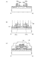
図7は、本発明の一態様のトランジスタ250の上面図および断面図である。図7(A
)は、上面図であり、図7(A)に示す一点鎖線A1−A2の断面が図7(B)に相当す
る。また、図7(C)は、図7(B)に示す破線丸で囲まれた領域の拡大図である。なお
、図7(A)の上面図では、図の明瞭化のために一部の要素を省いて図示している。
7A to 7C are a top view and cross-sectional views of the
) Is a top view, and a cross section taken along one-dot chain line A1-A2 shown in FIG. 7A corresponds to FIG. FIG. 7C is an enlarged view of a region surrounded by a broken-line circle shown in FIG. Note that in the top view of FIG. 7A, some elements are omitted for clarity.
図7に示すトランジスタ250は、基板100上の下地絶縁膜102と、下地絶縁膜1
02上の酸化物膜204aと、酸化物膜204a上の酸化物半導体膜204bと、酸化物
半導体膜204b上の酸化物膜204cと、酸化物膜204c上のハードマスク106a
およびハードマスク106bと、ハードマスク106a上のハードマスク108aと、ハ
ードマスク106b上のハードマスク108bと、下地絶縁膜102、酸化物膜204a
、酸化物半導体膜204b、酸化物膜204c、ハードマスク106aおよびハードマス
ク108a上のソース電極110aと、下地絶縁膜102、酸化物膜204a、酸化物半
導体膜204b、酸化物膜204c、ハードマスク106bおよびハードマスク108b
上のドレイン電極110bと、酸化物膜204a、酸化物半導体膜204b、酸化物膜2
04c、ハードマスク106a、ハードマスク106b、ハードマスク108a、ハード
マスク108b、ソース電極110aおよびドレイン電極110b上のゲート絶縁膜11
2と、ゲート絶縁膜112上のゲート電極114と、を有する。なお、ハードマスク10
6aおよびハードマスク106bは、導電性を有する膜とする。また、酸化物膜204a
、酸化物半導体膜204b、酸化物膜204cはまとめて多層膜204とよぶことがある
。多層膜204の、ハードマスク106a、ハードマスク106b、ソース電極110a
およびドレイン電極110bと接する領域には、低抵抗領域121aおよび低抵抗領域1
21bが形成される。また、ゲート絶縁膜112およびゲート電極114上に絶縁膜11
6が設けられていてもよい。絶縁膜116は必要に応じて設ければよく、さらにその上部
に他の絶縁膜を設けてもよい。
7 includes a
02, the
The
, The
04c,
2 and a
The 6a and the
The
In the region in contact with the
21b is formed. Further, the insulating film 11 is formed on the
6 may be provided. The insulating
また、酸化物膜204a、酸化物半導体膜204b、酸化物膜204cに用いる材料に
よっては、酸化物膜204aおよび酸化物半導体膜204bの境界、酸化物半導体膜20
4bおよび酸化物膜204cの境界を明確に確認できない場合がある。そこで、図におい
て、酸化物膜204a、酸化物半導体膜204b、酸化物膜204cの境界は破線で表し
ている。
Further, depending on the material used for the
In some cases, the boundary between 4b and the
実施の形態1に示すトランジスタ150と図7に示すトランジスタ250との違いは、
酸化物半導体膜の上下に酸化物膜を有しているか否かの点である。それ以外の構成につい
ては、実施の形態1を参酌することができる。
The difference between the
The point is whether or not oxide films are provided above and below the oxide semiconductor film.
酸化物膜204a、酸化物半導体膜204bおよび酸化物膜204cは、Inもしくは
Gaの一方、または両方を含む。代表的には、In−Ga酸化物(InとGaを含む酸化
物)、In−Zn酸化物(InとZnを含む酸化物)、In−M−Zn酸化物(Inと、
元素Mと、Znを含む酸化物。元素Mは、Al、Ti、Ga、Y、Zr、Sn、La、C
e、NdまたはHfから選ばれた1種類以上の元素)がある。
The
An oxide containing the element M and Zn. The element M is Al, Ti, Ga, Y, Zr, Sn, La, C
e, one or more elements selected from Nd or Hf).
酸化物膜204aおよび酸化物膜204cは、酸化物半導体膜204bを構成する金属
元素のうち、1種類以上の同じ金属元素を含む材料により形成されることが好ましい。こ
のような材料を用いることで、酸化物半導体膜204bと、酸化物膜204aおよび酸化
物膜204cとの界面に界面準位を生じにくくすることができる。従って、界面における
キャリアの散乱や捕獲が生じにくく、トランジスタの電界効果移動度を向上させることが
可能となる。また、トランジスタのしきい値電圧のばらつきを低減することが可能となる
。
The
また、酸化物膜204aおよび酸化物膜204cは、伝導帯下端のエネルギーが酸化物
半導体膜204bよりも、0.05eV、0.07eV、0.1eV、0.15eVのい
ずれか以上であって、2eV、1eV、0.5eV、0.4eVのいずれか以下の範囲で
真空準位に近い酸化物半導体で形成することが好ましい。
The
このような構造において、ゲート電極114に電界を印加すると、多層膜204のうち
、伝導帯下端のエネルギーが最も小さい酸化物半導体膜204bにチャネルが形成される
。すなわち、酸化物半導体膜204bとゲート絶縁膜112との間に酸化物膜204cが
形成されていることによって、トランジスタのチャネルをゲート絶縁膜と接しない構造と
することができる。
In such a structure, when an electric field is applied to the
また、酸化物膜204a、酸化物半導体膜204bおよび酸化物膜204cに用いる材
料によっては、酸化物膜204a、酸化物半導体膜204bおよび酸化物膜204cの境
界を明確に確認できない場合がある。そこで、図面において、酸化物半導体膜204bは
、酸化物膜204aおよび酸化物膜204cと異なるハッチングで表している。
Further, depending on the material used for the
酸化物膜204aの厚さは、3nm以上50nm以下、好ましくは3nm以上20nm
以下とする。酸化物半導体膜204bの厚さは、3nm以上200nm以下、好ましくは
3nm以上100nm以下、さらに好ましくは3nm以上50nm以下とする。酸化物膜
204cの厚さは、3nm以上100nm以下、好ましくは3nm以上50nm以下とす
る。
The thickness of the
The following. The thickness of the
また、酸化物半導体膜204bがIn−M−Zn酸化物であり、酸化物膜204aもI
n−M−Zn酸化物であるとき、酸化物膜204aをIn:M:Zn=x1:y1:z1
[原子数比]、酸化物半導体膜204bをIn:M:Zn=x2:y2:z2[原子数比
]とすると、y1/x1がy2/x2よりも大きくなる酸化物半導体膜204bおよび酸
化物膜204aを選択する。なお、元素MはInよりも酸素との結合力が強い金属元素で
あり、例えばAl、Ti、Ga、Y、Zr、Sn、La、Ce、NdまたはHfなどが挙
げられる。好ましくは、y1/x1がy2/x2よりも1.5倍以上大きくなる酸化物半
導体膜204bおよび酸化物膜204aを選択する。さらに好ましくは、y1/x1がy
2/x2よりも2倍以上大きくなる酸化物半導体膜204bおよび酸化物膜204aを選
択する。より好ましくは、y1/x1がy2/x2よりも3倍以上大きくなる酸化物半導
体膜204bおよび酸化物膜204aを選択する。このとき、酸化物半導体膜204bに
おいて、y1がx1以上であるとトランジスタに安定した電気特性を付与できるため好ま
しい。ただし、y1がx1の3倍以上になると、トランジスタの電界効果移動度が低下し
てしまうため、y1はx1の3倍未満であると好ましい。酸化物膜204aを上記構成と
することにより、酸化物膜204aを酸化物半導体膜204bよりも酸素欠損が生じにく
い膜とすることができる。
The
In the case of an n-M-Zn oxide, the
[Atom ratio] When the
The
また、酸化物半導体膜204bがIn−M−Zn酸化物であるとき、ZnおよびOを除
いてのInおよびMの原子数比率は、好ましくはInが25原子%以上、Mが75原子%
未満、さらに好ましくはInが34原子%以上、Mが66原子%未満とする。また、酸化
物膜204aがIn−M−Zn酸化物であるとき、ZnおよびOを除いてのInおよびM
の原子数比率は、好ましくはInが50原子%未満、Mが50原子%以上、さらに好まし
くはInが25原子%未満、Mが75原子%以上とする。
In the case where the
And more preferably, In is 34 atomic% or more and M is less than 66 atomic%. In addition, when the
Preferably, In is less than 50 atomic%, M is 50 atomic% or more, more preferably In is less than 25 atomic%, and M is 75 atomic% or more.
例えば、酸化物半導体膜204bとしてIn:Ga:Zn=1:1:1または3:1:
2の原子数比のIn−Ga−Zn酸化物を用いることができ、酸化物膜204aとしてI
n:Ga:Zn=1:3:2、1:3:4、1:6:2、1:6:4、1:6:10、1
:9:6、または1:9:0の原子数比のIn−Ga−Zn酸化物を用いることができる
。なお、酸化物半導体膜204bおよび酸化物膜204aの原子数比はそれぞれ、誤差と
して上記の原子数比のプラスマイナス20%の変動を含む。
For example, as the
An In—Ga—Zn oxide having an atomic ratio of 2 can be used, and the
n: Ga: Zn = 1: 3: 2, 1: 3: 4, 1: 6: 2, 1: 6: 4, 1: 6: 10, 1
: In: Ga-Zn oxide with an atomic ratio of 9: 6 or 1: 9: 0 can be used. Note that the atomic ratio of the
また、酸化物半導体膜204bがIn−M−Zn酸化物であり、酸化物膜204cもI
n−M−Zn酸化物であるとき、酸化物膜204cをIn:M:Zn=x1:y1:z1
[原子数比]、酸化物半導体膜204bをIn:M:Zn=x2:y2:z2[原子数比
]とすると、y1/x1がy2/x2よりも大きくなる酸化物半導体膜204bおよび酸
化物膜204cを選択する。なお、元素MはInよりも酸素との結合力が強い金属元素で
あり、例えばAl、Ti、Ga、Y、Zr、Sn、La、Ce、NdまたはHfなどが挙
げられる。好ましくは、y1/x1がy2/x2よりも1.5倍以上大きくなる酸化物半
導体膜204bおよび酸化物膜204cを選択する。さらに好ましくは、y1/x1がy
2/x2よりも2倍以上大きくなる酸化物半導体膜204bおよび酸化物膜204cを選
択する。より好ましくは、y1/x1がy2/x2よりも3倍以上大きくなる酸化物半導
体膜204bおよび酸化物膜204cを選択する。このとき、酸化物半導体膜204bに
おいて、y1がx1以上であるとトランジスタに安定した電気特性を付与できるため好ま
しい。ただし、y1がx1の3倍以上になると、トランジスタの電界効果移動度が低下し
てしまうため、y1はx1の3倍未満であると好ましい。酸化物膜204cを上記構成と
することにより、酸化物膜204cを酸化物半導体膜204bよりも酸素欠損が生じにく
い膜とすることができる。
The
In the case of an n-M-Zn oxide, the
[Atom ratio] When the
The
また、酸化物半導体膜204bがIn−M−Zn酸化物であるとき、ZnおよびOを除
いてのInおよびMの原子数比率は、好ましくはInが25原子%以上、Mが75原子%
未満、さらに好ましくはInが34原子%以上、Mが66原子%未満とする。また、酸化
物膜204cがIn−M−Zn酸化物であるとき、ZnおよびOを除いてのInおよびM
の原子数比率は、好ましくはInが50原子%未満、Mが50原子%以上、さらに好まし
くはInが25原子%未満、Mが75原子%以上とする。
In the case where the
And more preferably, In is 34 atomic% or more and M is less than 66 atomic%. In addition, when the
Preferably, In is less than 50 atomic%, M is 50 atomic% or more, more preferably In is less than 25 atomic%, and M is 75 atomic% or more.
例えば、酸化物半導体膜204bとしてIn:Ga:Zn=1:1:1または3:1:
2の原子数比のIn−Ga−Zn酸化物を用いることができ、酸化物膜204cとしてI
n:Ga:Zn=1:3:2、1:3:4、1:6:2、1:6:4、1:6:10、1
:9:6、または1:9:0の原子数比のIn−Ga−Zn酸化物を用いることができる
。なお、酸化物半導体膜204bおよび酸化物膜204cの原子数比はそれぞれ、誤差と
して上記の原子数比のプラスマイナス20%の変動を含む。
For example, as the
An In—Ga—Zn oxide having an atomic ratio of 2 can be used, and the
n: Ga: Zn = 1: 3: 2, 1: 3: 4, 1: 6: 2, 1: 6: 4, 1: 6: 10, 1
: In: Ga-Zn oxide with an atomic ratio of 9: 6 or 1: 9: 0 can be used. Note that the atomic ratio of the
多層膜204を用いたトランジスタに安定した電気特性を付与するためには、酸化物半
導体膜204b中の酸素欠損および不純物濃度を低減し、酸化物半導体膜204bを真性
または実質的に真性とみなせる半導体膜とすることが好ましい。特に、酸化物半導体膜2
04b中のチャネル形成領域が、真性または実質的に真性とみなせることが好ましい。具
体的には、酸化物半導体膜204bのキャリア密度を、1×10¹⁷/cm3未満、1×
1015/cm3未満、または1×1013/cm3未満とする。
In order to impart stable electric characteristics to the transistor including the
It is preferable that the channel formation region in 04b can be regarded as intrinsic or substantially intrinsic. Specifically, the carrier density of the
It is less than 10 15 / cm 3 or less than 1 × 10 13 / cm 3 .
また、酸化物半導体膜204bにおいて、水素、窒素、炭素、シリコン、および主成分
以外の金属元素は不純物となる。酸化物半導体膜204b中の不純物濃度を低減するため
には、近接する酸化物膜204aおよび酸化物膜204c中の不純物濃度も酸化物半導体
膜204bと同程度まで低減することが好ましい。
In the
特に、酸化物半導体膜204bにシリコンが高濃度で含まれることにより、シリコンに
起因する不純物準位が酸化物半導体膜204bに形成される。該不純物準位は、トラップ
準位となり、トランジスタの電気特性を劣化させることがある。トランジスタの電気特性
の劣化を小さくするためには、酸化物半導体膜204bのシリコン濃度を1×10¹⁹a
toms/cm3未満、好ましくは5×1018atoms/cm3未満、さらに好まし
くは1×10¹⁸atoms/cm3未満とすればよい。また、酸化物半導体膜204b
と酸化物膜204aおよび酸化物膜204cとの界面のシリコン濃度についても上記シリ
コン濃度の範囲とする。
In particular, when the
It may be less than toms / cm 3 , preferably less than 5 × 10 18 atoms / cm 3 , more preferably less than 1 × 10 18 atoms / cm 3 . In addition, the
The silicon concentration at the interface between the
なお、トランジスタのゲート絶縁膜としては、シリコンを含む絶縁膜が多く用いられる
ため、上記理由により酸化物半導体膜のチャネルとなる領域は絶縁膜と接しないことが好
ましい。また、ゲート絶縁膜と酸化物半導体膜との界面にチャネルが形成される場合、該
界面でキャリアの散乱が起こり、トランジスタの電界効果移動度が低くなることがある。
このような観点からも、酸化物半導体膜のチャネルとなる領域はゲート絶縁膜から離すこ
とが好ましい。
Note that since an insulating film containing silicon is often used as a gate insulating film of a transistor, a region serving as a channel of the oxide semiconductor film is preferably not in contact with the insulating film for the above reason. In the case where a channel is formed at the interface between the gate insulating film and the oxide semiconductor film, carrier scattering occurs at the interface, and the field-effect mobility of the transistor may be reduced.
From such a viewpoint, it is preferable that the region to be a channel of the oxide semiconductor film be separated from the gate insulating film.
したがって、多層膜204を酸化物膜204a、酸化物半導体膜204bおよび酸化物
膜204cの積層構造とすることで、トランジスタのチャネルが形成される酸化物半導体
膜204bをゲート絶縁膜112から離すことができ、高い電界効果移動度を有し、安定
した電気特性のトランジスタを形成することができる。
Therefore, when the
また、酸化物半導体膜204b中で水素および窒素は、ドナー準位を形成し、キャリア
密度を増大させてしまう。酸化物半導体膜204bを真性または実質的に真性とするため
には、酸化物半導体膜204b中の水素濃度は、SIMSにおいて、2×10²⁰ato
ms/cm3以下、好ましくは5×1019atoms/cm3以下、より好ましくは1
×1019atoms/cm3以下、さらに好ましくは5×1018atoms/cm3
以下とする。また、窒素濃度は、SIMSにおいて、5×10¹⁹atoms/cm3未
満、好ましくは5×10¹⁸atoms/cm3以下、より好ましくは1×1018at
oms/cm3以下、さらに好ましくは5×1017atoms/cm3以下とする。
In addition, hydrogen and nitrogen in the
ms / cm 3 or less, preferably 5 × 10 19 atoms / cm 3 or less, more preferably 1
× 10 19 atoms / cm 3 or less, more preferably 5 × 10 18 atoms / cm 3
The following. Further, the nitrogen concentration is less than 5 × 10 19 atoms / cm 3 , preferably 5 × 10 18 atoms / cm 3 or less, more preferably 1 × 10 18 at in SIMS.
oms / cm 3 or less, more preferably 5 × 10 17 atoms / cm 3 or less.
なお、酸化物半導体膜204bにシリコンおよび炭素が高い濃度で含まれることにより
、酸化物半導体膜204bの結晶性を低下させることがある。酸化物半導体膜204bの
結晶性を低下させないためには、酸化物半導体膜204bのシリコン濃度を1×10¹⁹
atoms/cm3未満、好ましくは5×1018atoms/cm3未満、さらに好ま
しくは1×10¹⁸atoms/cm3未満とすればよい。また、酸化物半導体膜204
bの結晶性を低下させないためには、酸化物半導体膜204bの炭素濃度を1×10¹⁹
atoms/cm3未満、好ましくは5×1018atoms/cm3未満、さらに好ま
しくは1×10¹⁸atoms/cm3未満とすればよい。
Note that when the
It may be less than atoms / cm 3 , preferably less than 5 × 10 18 atoms / cm 3 , more preferably less than 1 × 10 18 atoms / cm 3 . In addition, the
In order not to decrease the crystallinity of b, the carbon concentration of the
It may be less than atoms / cm 3 , preferably less than 5 × 10 18 atoms / cm 3 , more preferably less than 1 × 10 18 atoms / cm 3 .
また、酸化物半導体のバンドギャップは2eV以上あるため、酸化物半導体を用いたト
ランジスタは、トランジスタがオフ状態のときのリーク電流(オフ電流ともいう)を極め
て小さくすることができる。
In addition, since the band gap of an oxide semiconductor is 2 eV or more, a transistor including an oxide semiconductor can extremely reduce leakage current (also referred to as off-state current) when the transistor is off.
以下では、多層膜中の局在準位について説明する。多層膜中の局在準位密度を低減する
ことで、多層膜を用いたトランジスタに安定した電気特性を付与することができる。多層
膜の局在準位密度は、一定光電流測定法(CPM:Constant Photocur
rent Method)によって評価可能である。
Hereinafter, localized levels in the multilayer film will be described. By reducing the density of localized states in the multilayer film, stable electrical characteristics can be imparted to the transistor including the multilayer film. The localized level density of the multilayer film is determined by a constant photocurrent measurement method (CPM: Constant Photocur).
rent Method).
トランジスタに安定した電気特性を付与するためには、多層膜中のCPM測定で得られ
る局在準位による吸収係数を、1×10⁻³cm−1未満、好ましくは3×10⁻⁴cm
−1未満とすればよい。また、多層膜中のCPM測定で得られる局在準位による吸収係数
を、1×10⁻³cm−1未満、好ましくは3×10⁻⁴cm−1未満とすることで、ト
ランジスタの電界効果移動度を高めることができる。なお、多層膜中のCPM測定で得ら
れる局在準位による吸収係数を、1×10⁻³cm−1未満、好ましくは3×10⁻⁴c
m−1未満とするためには、酸化物半導体膜204b中で局在準位を形成する元素である
シリコン、ゲルマニウム、炭素などの濃度を2×10¹⁸atoms/cm3未満、好ま
しくは2×10¹⁷atoms/cm3未満とすればよい。
In order to impart stable electrical characteristics to the transistor, the absorption coefficient due to the localized level obtained by CPM measurement in the multilayer film is less than 1 × 10 −3 cm −1 , preferably 3 × 10 −4 cm.
It may be less than -1 . Further, the field effect of the transistor can be obtained by setting the absorption coefficient due to the localized level obtained by CPM measurement in the multilayer film to be less than 1 × 10 −3 cm −1 , preferably less than 3 × 10 −4 cm −1. Mobility can be increased. In addition, the absorption coefficient by the localized level obtained by CPM measurement in the multilayer film is less than 1 × 10 −3 cm −1 , preferably 3 × 10 −4 c.
In order to make it less than m −1 , the concentration of silicon, germanium, carbon, or the like, which is an element forming a localized level in the
なお、CPM測定では、試料である多層膜に接して設けられた電極間に電圧を印加した
状態で光電流値が一定となるように端子間の試料面に照射する光量を調整し、照射光量か
ら吸収係数を導出することを各波長にて行う測定である。CPM測定において、試料に欠
陥があるとき、欠陥の存在する準位に応じたエネルギー(波長より換算)における吸収係
数が増加する。この吸収係数の増加分に定数を掛けることにより、試料の欠陥密度を導出
することができる。
In CPM measurement, the amount of light applied to the sample surface between the terminals is adjusted so that the photocurrent value is constant while a voltage is applied between the electrodes provided in contact with the multilayer film that is the sample, In this measurement, the absorption coefficient is derived from each wavelength. In CPM measurement, when a sample has a defect, an absorption coefficient at an energy (converted from a wavelength) corresponding to the level where the defect exists is increased. By multiplying the increase in the absorption coefficient by a constant, the defect density of the sample can be derived.
CPM測定で得られた局在準位は、不純物や欠陥に起因する準位と考えられる。すなわ
ち、CPM測定で得られる局在準位による吸収係数が小さい多層膜を用いることでトラン
ジスタに安定した電気特性を付与することができる。
Localized levels obtained by CPM measurement are considered to be levels caused by impurities and defects. That is, stable electrical characteristics can be imparted to the transistor by using a multilayer film having a small absorption coefficient due to localized levels obtained by CPM measurement.
次に、トランジスタ250の作製方法について図8乃至図10を用いて説明する。
Next, a method for manufacturing the
まずは、基板100を準備する。次に、下地絶縁膜102を形成する。その後、下地絶
縁膜102上に酸化物膜203a、酸化物半導体膜203bおよび酸化物膜203cを順
に成膜する(図8(A)参照)。なお、酸化物膜203a、酸化物半導体膜203b、酸
化物膜203cはまとめて多層膜203とよぶことがある。
First, the
基板100および下地絶縁膜102の材料および作製方法は、実施の形態1を参酌する
ことができる。酸化物膜203a、酸化物半導体膜203bおよび酸化物膜203cの材
料は、先に示した酸化物膜204a、酸化物半導体膜204bおよび酸化物膜204cの
材料を用いることができ、酸化物膜203a、酸化物半導体膜203bおよび酸化物膜2
03cの作製方法は、実施の形態1の酸化物半導体膜103を参酌することができる。
For the manufacturing method of 03c, the
次に、第1の熱処理を行うと好ましい。第1の熱処理は、250℃以上650℃以下、
好ましくは300℃以上500℃以下で行えばよい。第1の熱処理の雰囲気は、不活性ガ
ス雰囲気、酸化性ガスを10ppm以上、好ましくは1%以上さらに好ましくは10%以
上含む雰囲気、または減圧状態で行う。または、第1の熱処理の雰囲気は、不活性ガス雰
囲気で熱処理した後に、脱離した酸素を補うために酸化性ガスを10ppm以上、好まし
くは1%以上さらに好ましくは10%以上含む雰囲気で熱処理を行ってもよい。第1の熱
処理によって、酸化物半導体膜203bの結晶性を高め、さらに後に形成されるゲート絶
縁膜および酸化物半導体膜から水、水素、窒素、および炭素などの不純物を除去すること
ができる。
Next, it is preferable to perform a first heat treatment. The first heat treatment is 250 ° C. or higher and 650 ° C. or lower,
Preferably, it may be performed at 300 ° C. or higher and 500 ° C. or lower. The atmosphere for the first heat treatment is an inert gas atmosphere, an atmosphere containing an oxidizing gas of 10 ppm or more, preferably 1% or more, more preferably 10% or more, or a reduced pressure state. Alternatively, the atmosphere of the first heat treatment is heat treatment in an atmosphere containing an oxidizing gas of 10 ppm or more, preferably 1% or more, more preferably 10% or more to supplement the desorbed oxygen after heat treatment in an inert gas atmosphere. You may go. By the first heat treatment, the crystallinity of the
次に、酸化物膜203c上にハードマスク105、ハードマスク107を成膜し、ハー
ドマスク107上にレジストを形成し、該レジストに対して電子ビームを用いた露光を行
い、レジストマスク122を形成する(図8(B)参照)。なお、ハードマスク105は
、酸化物半導体膜を構成する金属元素よりも酸素と結合しやすく、導電性を有する膜であ
る。そのため、このとき、ハードマスク105の材料が酸素と結合しやすい導電材料であ
るため、多層膜203中の酸素が導電材料(ハードマスク105)と結合する。この結合
により、多層膜203の、ハードマスク105との界面近傍の領域において酸素が欠損す
る。または、多層膜203上に形成されるハードマスク105を形成する際の多層膜20
3上面へのダメージ(酸素欠損)が生じる。これらの酸素欠損により、低抵抗領域120
が形成される。
Next, a
3 Damage to the upper surface (oxygen deficiency) occurs. Due to these oxygen vacancies, the low-
Is formed.
また、電子ビームを用いた露光にかえてArFエキシマレーザを光源とする液浸露光や
、EUV露光を用いてもよい。
Further, immersion exposure using an ArF excimer laser as a light source or EUV exposure may be used instead of exposure using an electron beam.
ハードマスク105、ハードマスク107およびレジストマスク122の材料および作
製方法は、実施の形態1を参酌することができる。
次に、レジストマスク122をマスクにして、ハードマスク105およびハードマスク
107を選択的にエッチングし、ハードマスク106およびハードマスク108を形成す
る(図8(C)参照)。その後、レジストマスク122を除去する。エッチングする条件
やレジストマスク122の除去処理等は実施の形態1を参酌することができる。
Next, using the resist
次に、ハードマスク106およびハードマスク108をマスクにして、多層膜203を
選択的にエッチングし、多層膜204(酸化物膜204a、酸化物半導体膜204bおよ
び酸化物膜204c)および低抵抗領域120aを形成する(図9(A)参照)。
Next, the
次に、下地絶縁膜102、多層膜204、ハードマスク106およびハードマスク10
8上にソース電極110aおよびドレイン電極110bとなる導電膜を成膜し、導電膜の
一部を加工してソース電極110aおよびドレイン電極110bを形成する(図9(B)
参照)。導電膜の材料および作製方法は、実施の形態1を参酌することができる。
Next, the
8, a conductive film to be the
reference).
なお、ソース電極110aおよびドレイン電極110bとなる導電膜の材料は酸化物半
導体膜を構成する金属元素よりも酸素と結合しやすい導電材料を用いる。このとき、導電
膜の材料が酸素と結合しやすい導電材料であるため、多層膜204中の酸素が導電材料(
導電膜)と結合する。この結合により、多層膜204の、導電膜との界面近傍の領域にお
いて酸素が欠損する。または、多層膜204上(側面)に形成される導電膜を形成する際
の多層膜204上面(側面)へのダメージ(酸素欠損)が生じる。これらの酸素欠損によ
り、低抵抗領域120bが形成される。なお、本実施の形態では、低抵抗領域120bと
多層膜204との境界は酸化物膜204c中に存在するがこれに限られず、該境界は、酸
化物膜204a中、酸化物半導体膜204b中、酸化物膜204aと酸化物半導体膜20
4bとの界面、または酸化物半導体膜204bと酸化物膜204cとの界面に存在しても
よい。また、低抵抗領域120bは、多層膜204と導電膜との界面から多層膜204の
深さ方向に0nmより大きく15nm以下、好ましくは10nm未満、さらに好ましくは
3nm未満の領域にある。
Note that a conductive material that is more easily bonded to oxygen than a metal element included in the oxide semiconductor film is used as a material for the conductive film to be the
A conductive film). By this bonding, oxygen is lost in a region of the
4b or at the interface between the
低抵抗領域120bが形成されることにより、ソース電極110aまたはドレイン電極
110bと、多層膜204との接触抵抗を低減することができ、トランジスタ250の高
速動作を実現することができる。
By forming the
次に、レジストマスク122と同様に、ハードマスク108、ソース電極110aおよ
びドレイン電極110b上にレジストを形成し、該レジストに対して電子ビームを用いた
露光を行い、レジストマスク124を形成する(図9(C)参照)。
Next, similarly to the resist
また、電子ビームを用いた露光にかえてArFエキシマレーザを光源とする液浸露光や
、EUV露光を用いてもよい。
Further, immersion exposure using an ArF excimer laser as a light source or EUV exposure may be used instead of exposure using an electron beam.
次に、レジストマスク124をマスクにして、ハードマスク106およびハードマスク
108を選択的にエッチングし、ハードマスク106a、ハードマスク106b、ハード
マスク108aおよびハードマスク108bを形成する(図10(A)参照)。その後、
レジストマスク124を除去する。エッチングする条件やレジストマスク124の除去処
理等は実施の形態1を参酌することができる。
Next, using the resist
The resist
次に、ゲート絶縁膜112を形成する(図10(B)参照)。ゲート絶縁膜112の材
料および作製方法は、実施の形態1を参酌することができる。
Next, the
次に、多層膜204のチャネル形成領域となる領域Aに対して酸素130を添加し、低
抵抗領域121aおよび低抵抗領域121bを形成する。酸素130の添加方法および添
加条件等は実施の形態1を参酌することができる。
Next,
次に、第2の熱処理を行うことが好ましい。第2の熱処理は、第1の熱処理と同様の条
件で行うことができる。第2の熱処理により、多層膜204から、さらに水素や水などの
不純物を除去することができる。
Next, it is preferable to perform a second heat treatment. The second heat treatment can be performed under the same conditions as the first heat treatment. By the second heat treatment, impurities such as hydrogen and water can be further removed from the
次に、ゲート絶縁膜112上にゲート電極114となる導電膜を成膜し、導電膜の一部
を加工してゲート電極114を形成する。ゲート電極114の材料および作製方法は、実
施の形態1を参酌することができる。
Next, a conductive film to be the
次に、第3の熱処理を行うことが好ましい。第3の熱処理は、第1の熱処理と同様の条
件で行うことができる。酸素が過剰に含まれている下地絶縁膜102、絶縁膜116の場
合、第3の熱処理により、下地絶縁膜102、絶縁膜116から過剰な酸素が放出されや
すくなり、多層膜204、特に酸化物半導体膜204bの酸素欠損を低減することができ
る。よって、多層膜204のチャネル形成領域は、さらに酸素欠損量が低減し、高純度真
性化となる。
Next, it is preferable to perform a third heat treatment. The third heat treatment can be performed under the same conditions as the first heat treatment. In the case of the
以上により、トランジスタ250を作製することができる。
Through the above steps, the
また、トランジスタの別の構成を図11に示す。図11に示すトランジスタ260は、
基板100上の下地絶縁膜102と、下地絶縁膜102上の酸化物膜204aと、酸化物
膜204a上の酸化物半導体膜204bと、酸化物半導体膜204b上のハードマスク1
06aおよびハードマスク106bと、ハードマスク106a上のハードマスク108a
と、ハードマスク106b上のハードマスク108bと、下地絶縁膜102、酸化物膜2
04a、酸化物半導体膜204b、ハードマスク106aおよびハードマスク108a上
のソース電極110aと、下地絶縁膜102、酸化物膜204a、酸化物半導体膜204
b、ハードマスク106bおよびハードマスク108b上のドレイン電極110bと、酸
化物膜204a、酸化物半導体膜204b、ハードマスク106a、ハードマスク106
b、ハードマスク108a、ハードマスク108b、ソース電極110aおよびドレイン
電極110b上の酸化物膜204cと、酸化物膜204c上のゲート絶縁膜112と、ゲ
ート絶縁膜112上のゲート電極114と、を有する。また、ゲート絶縁膜112および
ゲート電極114上に絶縁膜116が設けられていてもよい。絶縁膜116は必要に応じ
て設ければよく、さらにその上部に他の絶縁膜を設けてもよい。
FIG. 11 illustrates another structure of the transistor. The
The base
06a and
The
04a, the
b,
b, a
図7に示すトランジスタ250と図11に示すトランジスタ260とは、酸化物膜20
4cがソース電極110aおよびドレイン電極110b上に形成されている点が異なり、
その他の点は同じである。
The
4c is formed on the
The other points are the same.
トランジスタ260では、チャネルが形成される酸化物半導体膜204bとソース電極
およびドレイン電極の一部として機能するハードマスク106aおよびハードマスク10
6bが接しており、酸化物半導体膜204bに高密度の酸素欠損が生成し、n型化された
領域(低抵抗領域121aおよび低抵抗領域121b)が形成される。したがって、キャ
リアのパスに抵抗成分が少なく、効率良くキャリアを移動させることができる。
In the
6b is in contact, high-density oxygen vacancies are generated in the
なお、本実施の形態では、チャネルとは、ソース電極およびドレイン電極の間における
酸化物半導体膜のことをいう。また、チャネル形成領域とは、ソース電極およびドレイン
電極の間における多層膜のことをいう。
Note that in this embodiment, a channel refers to an oxide semiconductor film between a source electrode and a drain electrode. A channel formation region refers to a multilayer film between a source electrode and a drain electrode.
また、酸化物膜204cは、ソース電極110aおよびドレイン電極110b形成後に
形成するため、該ソース電極110aおよびドレイン電極110b形成時の酸化物膜20
4cのオーバーエッチングが無い。したがって、チャネルが形成される酸化物半導体膜2
04bをゲート絶縁膜112から十分離すことができ、界面からの不純物拡散の影響を抑
える効果を大きくすることができる。
Since the
There is no overetching of 4c. Therefore, the oxide semiconductor film 2 in which the channel is formed
04b can be sufficiently separated from the
また、酸化物膜204cは、外部から水素または水素を含む化合物(水など)が酸化物
半導体膜204bへと侵入することを抑制するバリア膜として機能するため、トランジス
タの信頼性を向上させることができる。
In addition, since the
このような作製方法を用いることで、酸化物半導体膜を島状に微細加工する際に、酸化
物半導体膜の側面の凹凸を抑制することができる。よって、微細な構造であっても高い電
気特性を有するトランジスタを歩留まりよく提供することができる。また、該トランジス
タを含む半導体装置においても、高性能化、高信頼性化、および高生産化を達成すること
ができる。
By using such a manufacturing method, unevenness on the side surface of the oxide semiconductor film can be suppressed when the oxide semiconductor film is finely processed into an island shape. Therefore, a transistor having high electrical characteristics even with a fine structure can be provided with high yield. In a semiconductor device including the transistor, high performance, high reliability, and high production can be achieved.
なお、本実施の形態は、本明細書で示す他の実施の形態と適宜組み合わせることができ
る。
Note that this embodiment can be combined with any of the other embodiments described in this specification as appropriate.
(実施の形態4)
本実施の形態では、本発明の一態様であるトランジスタを使用し、電力が供給されない
状況でも記憶内容の保持が可能で、かつ、書き込み回数にも制限が無い半導体装置(記憶
装置)の一例を、図面を用いて説明する。
(Embodiment 4)
In this embodiment, an example of a semiconductor device (memory device) that uses a transistor which is one embodiment of the present invention, can hold stored data even when power is not supplied, and has no limit on the number of writing times. This will be described with reference to the drawings.
図12(A)に半導体装置の断面図、図12(B)に半導体装置の回路図をそれぞれ示
す。
12A is a cross-sectional view of the semiconductor device, and FIG. 12B is a circuit diagram of the semiconductor device.
図12(A)および図12(B)に示す半導体装置は、下部に第1の半導体材料を用い
たトランジスタ400を有し、上部に第2の半導体材料を用いたトランジスタ402およ
び容量素子404を有している。なお、トランジスタ402としては、先の実施の形態で
説明したトランジスタを用いることができ、本実施の形態では、実施の形態1の図1に示
すトランジスタ150を適用する例を示している。また、容量素子404は、一方の電極
をトランジスタ402のゲート電極、他方の電極をトランジスタ402のソース電極また
はドレイン電極、誘電体をトランジスタ402のゲート絶縁膜と同じ材料を用いる構造と
することで、トランジスタ402と同時に形成することができる。
The semiconductor device illustrated in FIGS. 12A and 12B includes a
ここで、第1の半導体材料と第2の半導体材料は異なる禁制帯幅を持つ材料とすること
が望ましい。例えば、第1の半導体材料を酸化物半導体以外の半導体材料(シリコンなど
)とし、第2の半導体材料を実施の形態1で説明した酸化物半導体とすることができる。
酸化物半導体以外の材料を用いたトランジスタは、高速動作が容易である。一方で、酸化
物半導体を用いたトランジスタは、オフ電流が低い電気特性により長時間の電荷保持を可
能とする。
Here, it is desirable that the first semiconductor material and the second semiconductor material have different band gaps. For example, the first semiconductor material can be a semiconductor material other than an oxide semiconductor (such as silicon), and the second semiconductor material can be the oxide semiconductor described in
A transistor including a material other than an oxide semiconductor can easily operate at high speed. On the other hand, a transistor including an oxide semiconductor can hold charge for a long time because of electrical characteristics with low off-state current.
なお、上記トランジスタは、いずれもnチャネル型トランジスタであるものとして説明
するが、pチャネル型トランジスタを用いることができるのはいうまでもない。また、情
報を保持するために酸化物半導体を用いた先の実施の形態に示すようなトランジスタを用
いる他は、半導体装置に用いられる材料や半導体装置の構造など、半導体装置の具体的な
構成をここで示すものに限定する必要はない。
Note that although all the above transistors are described as n-channel transistors, it goes without saying that p-channel transistors can be used. In addition to using a transistor such as that described in the above embodiment using an oxide semiconductor to retain information, a specific structure of a semiconductor device such as a material used in the semiconductor device or a structure of the semiconductor device is used. It is not necessary to limit to what is shown here.
図12(A)におけるトランジスタ400は、半導体材料(例えば、結晶性シリコンな
ど)を含む基板410に設けられたチャネル形成領域と、チャネル形成領域を挟むように
設けられた不純物領域と、不純物領域に接する金属間化合物領域と、チャネル形成領域上
に設けられたゲート絶縁膜と、ゲート絶縁膜上に設けられたゲート電極と、を有する。な
お、図において、明示的にはソース電極やドレイン電極を有しない場合があるが、便宜上
、このような状態を含めてトランジスタと呼ぶ場合がある。また、この場合、トランジス
タの接続関係を説明するために、ソース領域やドレイン領域を含めてソース電極やドレイ
ン電極と表現することがある。つまり、たとえば、本明細書において、ソース電極との記
載には、ソース領域が含まれうる。
A
基板410上にはトランジスタ400を囲むように素子分離絶縁層406が設けられて
おり、トランジスタ400を覆うように絶縁膜420が設けられている。なお、素子分離
絶縁層406は、LOCOS(Local Oxidation of Silicon
)や、STI(Shallow Trench Isolation)などの素子分離技
術を用いて形成することができる。
An element
) And STI (Shallow Trench Isolation).
例えば、結晶性シリコン基板を用いたトランジスタ400は、高速動作が可能である。
このため、当該トランジスタを読み出し用のトランジスタとして用いることで、情報の読
み出しを高速に行うことができる。トランジスタ402および容量素子404の形成前の
処理として、トランジスタ400を覆う絶縁膜420にCMP処理を施して、絶縁膜42
0を平坦化すると同時にトランジスタ400のゲート電極の上面を露出させる。
For example, the
Therefore, information can be read at high speed by using the transistor as a reading transistor. As a process before the formation of the
While flattening 0, the upper surface of the gate electrode of the
絶縁膜420上にはトランジスタ402が設けられ、そのソース電極またはドレイン電
極の一方は延在して、容量素子404の一方の電極として作用する。
A
図12(A)に示すトランジスタ402は、酸化物半導体膜にチャネルが形成されるト
ップゲート型トランジスタである。トランジスタ402は、オフ電流が小さいため、これ
を用いることにより長期にわたり記憶内容を保持することが可能である。つまり、リフレ
ッシュ動作を必要としない、或いは、リフレッシュ動作の頻度が極めて少ない半導体記憶
装置とすることが可能となるため、消費電力を十分に低減することができる。
A
また、トランジスタ402において、ソース電極またはドレイン電極が接している酸化
物半導体膜の界面近傍の領域に低抵抗領域が形成され、ソース電極およびドレイン電極を
マスクにして、酸素を酸化物半導体膜に添加することで、チャネル形成領域を高純度かつ
真性な領域とすることができ、高純度かつ真性な領域と低抵抗領域を形成することができ
る。当該トランジスタは酸化物半導体膜中のチャネル形成領域における酸素欠損量を低減
することができ、電気特性が良好であるため、信頼性の高い半導体装置を提供することが
できる。
In the
図12(A)に示すように、トランジスタ400と容量素子404は重畳するように形
成することができるため、その占有面積を低減することができる。したがって、半導体装
置の集積度を高めることができる。
As illustrated in FIG. 12A, the
次に、図12(A)に対応する回路構成の一例を図12(B)に示す。 Next, FIG. 12B illustrates an example of a circuit configuration corresponding to FIG.
図12(B)において、第1の配線(1st Line)とトランジスタ400のソー
ス電極またはドレイン電極の一方とは、電気的に接続され、第2の配線(2nd Lin
e)とトランジスタ400のソース電極またはドレイン電極の他方とは、電気的に接続さ
れている。また、第3の配線(3rd Line)とトランジスタ402のソース電極ま
たはドレイン電極の一方とは、電気的に接続され、第4の配線(4th Line)と、
トランジスタ402のゲート電極とは、電気的に接続されている。そして、トランジスタ
400のゲート電極と、トランジスタ402のソース電極またはドレイン電極の他方は、
容量素子404の電極の一方と電気的に接続され、第5の配線(5th Line)と、
容量素子404の電極の他方は電気的に接続されている。
In FIG. 12B, the first wiring (1st Line) and one of the source electrode and the drain electrode of the
e) and the other of the source electrode and the drain electrode of the
The gate electrode of the
A fifth wiring (5th Line) electrically connected to one of the electrodes of the
The other electrode of the
図12(B)に示す半導体装置では、トランジスタ400のゲート電極の電位が保持可
能という特徴を活かすことで、次のように、情報の書き込み、保持、読み出しが可能であ
る。
In the semiconductor device illustrated in FIG. 12B, information can be written, held, and read as follows by utilizing the feature that the potential of the gate electrode of the
情報の書き込みおよび保持について説明する。まず、第4の配線の電位を、トランジス
タ402がオン状態となる電位にして、トランジスタ402をオン状態とする。これによ
り、第3の配線の電位が、トランジスタ400のゲート電極、および容量素子404に与
えられる。すなわち、トランジスタ400のゲート電極には、所定の電荷が与えられる(
書き込み)。ここでは、異なる二つの電位レベルを与える電荷(以下Lowレベル電荷、
Highレベル電荷という)のいずれかが与えられるものとする。その後、第4の配線の
電位を、トランジスタ402がオフ状態となる電位にして、トランジスタ402をオフ状
態とすることにより、トランジスタ400のゲート電極に与えられた電荷が保持される(
保持)。
Information writing and holding will be described. First, the potential of the fourth wiring is set to a potential at which the
writing). Here, a charge giving two different potential levels (hereinafter referred to as a Low level charge,
Any of high level charges) is given. After that, the potential of the fourth wiring is set to a potential at which the
Retention).
トランジスタ402のオフ電流は極めて小さいため、トランジスタ400のゲート電極
の電荷は長時間にわたって保持される。
Since the off-state current of the
次に情報の読み出しについて説明する。第1の配線に所定の電位(定電位)を与えた状
態で、第5の配線に適切な電位(読み出し電位)を与えると、トランジスタ400のゲー
ト電極に保持された電荷量に応じて、第2の配線は異なる電位をとる。一般に、トランジ
スタ400をnチャネル型とすると、トランジスタ400のゲート電極にHighレベル
電荷が与えられている場合の見かけのしきい値Vth_Hは、トランジスタ400のゲー
ト電極にLowレベル電荷が与えられている場合の見かけのしきい値Vth_Lより低く
なるためである。ここで、見かけのしきい値電圧とは、トランジスタ400を「オン状態
」とするために必要な第5の配線の電位をいうものとする。したがって、第5の配線の電
位をVth_HとVth_Lの間の電位V0とすることにより、トランジスタ400のゲ
ート電極に与えられた電荷を判別できる。例えば、書き込みにおいて、Highレベル電
荷が与えられていた場合には、第5の配線の電位がV0(>Vth_H)となれば、トラ
ンジスタ400は「オン状態」となる。Lowレベル電荷が与えられていた場合には、第
5の配線の電位がV0(<Vth_L)となっても、トランジスタ400は「オフ状態」
のままである。このため、第2の配線の電位を判別することで、保持されている情報を読
み出すことができる。
Next, reading of information will be described. When an appropriate potential (reading potential) is applied to the fifth wiring in a state where a predetermined potential (constant potential) is applied to the first wiring, the first wiring is changed according to the amount of charge held in the gate electrode of the
Remains. Therefore, the retained information can be read by determining the potential of the second wiring.
なお、メモリセルをアレイ状に配置して用いる場合、所望のメモリセルの情報のみを読
み出せることが必要になる。このように情報を読み出さない場合には、ゲート電極の状態
にかかわらずトランジスタ400が「オフ状態」となるような電位、つまり、Vth_H
より小さい電位を第5の配線に与えればよい。または、ゲート電極の状態にかかわらずト
ランジスタ400が「オン状態」となるような電位、つまり、Vth_Lより大きい電位
を第5の配線に与えればよい。
Note that in the case of using memory cells arranged in an array, it is necessary to read only information of a desired memory cell. In the case where information is not read out in this manner, a potential at which the
A smaller potential may be supplied to the fifth wiring. Alternatively, a potential at which the
本実施の形態に示す半導体装置では、チャネル形成領域に酸化物半導体を用いたオフ電
流の極めて小さいトランジスタを適用することで、極めて長期にわたり記憶内容を保持す
ることが可能である。つまり、リフレッシュ動作が不要となるか、または、リフレッシュ
動作の頻度を極めて低くすることが可能となるため、消費電力を十分に低減することがで
きる。また、電力の供給がない場合(ただし、電位は固定されていることが望ましい)で
あっても、長期にわたって記憶内容を保持することが可能である。
In the semiconductor device described in this embodiment, stored data can be held for an extremely long time by using a transistor with an extremely small off-state current that uses an oxide semiconductor for a channel formation region. That is, the refresh operation is not necessary or the frequency of the refresh operation can be extremely low, so that power consumption can be sufficiently reduced. In addition, stored data can be held for a long time even when power is not supplied (note that a potential is preferably fixed).
また、本実施の形態に示す半導体装置では、情報の書き込みに高い電圧を必要とせず、
素子の劣化の問題もない。例えば、従来の不揮発性メモリのように、フローティングゲー
トへの電子の注入や、フローティングゲートからの電子の引き抜きを行う必要がないため
、ゲート絶縁膜の劣化といった問題が全く生じない。すなわち、開示する発明に係る半導
体装置では、従来の不揮発性メモリで問題となっている書き換え可能回数に制限はなく、
信頼性が飛躍的に向上する。さらに、トランジスタのオン状態、オフ状態によって、情報
の書き込みが行われるため、高速な動作も容易に実現しうる。
In addition, in the semiconductor device described in this embodiment, high voltage is not required for writing data,
There is no problem of deterioration of the element. For example, unlike the conventional nonvolatile memory, it is not necessary to inject electrons into the floating gate or extract electrons from the floating gate, so that there is no problem of deterioration of the gate insulating film. That is, in the semiconductor device according to the disclosed invention, there is no limit to the number of rewritable times that is a problem in the conventional nonvolatile memory,
Reliability is dramatically improved. Further, since data is written depending on the on / off state of the transistor, high-speed operation can be easily realized.
以上のように、微細化および高集積化を実現し、かつ高い電気的特性を付与された半導
体装置、および該半導体装置の作製方法を提供することができる。
As described above, a semiconductor device that achieves miniaturization and high integration and is provided with high electrical characteristics, and a method for manufacturing the semiconductor device can be provided.
なお、本実施の形態は、本明細書で示す他の実施の形態と適宜組み合わせることができ
る。
Note that this embodiment can be combined with any of the other embodiments described in this specification as appropriate.
(実施の形態5)
本実施の形態では、本発明の一態様であるトランジスタを使用し、電力が供給されない
状況でも記憶内容の保持が可能で、かつ、書き込み回数にも制限が無い半導体装置につい
て、実施の形態4に示した構成と異なる半導体装置の説明を行う。
(Embodiment 5)
In this embodiment, a semiconductor device which uses a transistor which is one embodiment of the present invention, can hold stored data even in a state where power is not supplied, and has no limit on the number of times of writing is described in Embodiment 4. A description will be given of a semiconductor device different from the structure shown.
図13(A)は、半導体装置の回路構成の一例を示し、図13(B)は半導体装置の一
例を示す概念図である。なお、当該半導体装置に含まれるトランジスタ562としては、
先の実施の形態で説明したトランジスタを用いることができる。また、容量素子554は
、実施の形態4で説明した容量素子404と同様に、トランジスタ562の作製工程にて
同時に作製することができる。
FIG. 13A illustrates an example of a circuit configuration of a semiconductor device, and FIG. 13B is a conceptual diagram illustrating an example of a semiconductor device. Note that as the
The transistor described in the above embodiment can be used. Further, the
図13(A)に示す半導体装置において、ビット線BLとトランジスタ562のソース
電極とは電気的に接続され、ワード線WLとトランジスタ562のゲート電極とは電気的
に接続され、トランジスタ562のドレイン電極と容量素子554の一方の端子とは電気
的に接続されている。
In the semiconductor device illustrated in FIG. 13A, the bit line BL and the source electrode of the
次に、図13(A)に示す半導体装置(メモリセル550)に、情報の書き込みおよび
保持を行う場合について説明する。
Next, the case where data is written and held in the semiconductor device (memory cell 550) illustrated in FIG. 13A is described.
まず、ワード線WLの電位を、トランジスタ562がオン状態となる電位として、トラ
ンジスタ562をオン状態とする。これにより、ビット線BLの電位が、容量素子554
の一方の端子に与えられる(書き込み)。その後、ワード線WLの電位を、トランジスタ
562がオフ状態となる電位として、トランジスタ562をオフ状態とすることにより、
容量素子554の一方の端子の電位が保持される(保持)。
First, the potential of the word line WL is set to a potential at which the
(Write). After that, the potential of the word line WL is set to a potential at which the
The potential of one terminal of the
酸化物半導体を用いたトランジスタ562は、オフ電流が極めて小さいという特徴を有
している。このため、トランジスタ562をオフ状態とすることで、容量素子554の第
1の端子の電位(あるいは、容量素子554に蓄積された電荷)を極めて長時間にわたっ
て保持することが可能である。
The
次に、情報の読み出しについて説明する。トランジスタ562がオン状態となると、浮
遊状態であるビット線BLと容量素子554とが導通し、ビット線BLと容量素子554
の間で電荷が再分配される。その結果、ビット線BLの電位が変化する。ビット線BLの
電位の変化量は、容量素子554の第1の端子の電位(あるいは容量素子554に蓄積さ
れた電荷)によって、異なる値をとる。
Next, reading of information will be described. When the
The charge is redistributed between the two. As a result, the potential of the bit line BL changes. The amount of change in the potential of the bit line BL varies depending on the potential of the first terminal of the capacitor 554 (or the charge accumulated in the capacitor 554).
例えば、容量素子554の第1の端子の電位をV、容量素子554の容量をC、ビット
線BLが有する容量成分(以下、ビット線容量とも呼ぶ)をCB、電荷が再分配される前
のビット線BLの電位をVB0とすると、電荷が再分配された後のビット線BLの電位は
、(CB×VB0+C×V)/(CB+C)となる。したがって、メモリセル550の状
態として、容量素子554の第1の端子の電位がV1とV0(V1>V0)の2状態をと
るとすると、電位V1を保持している場合のビット線BLの電位(=(CB×VB0+C
×V1)/(CB+C))は、電位V0を保持している場合のビット線BLの電位(=(
CB×VB0+C×V0)/(CB+C))よりも高くなることがわかる。
For example, the potential of the first terminal of the
× V1) / (CB + C)) is the potential of the bit line BL when the potential V0 is held (= (
It can be seen that it is higher than (CB × VB0 + C × V0) / (CB + C)).
そして、ビット線BLの電位を所定の電位と比較することで、情報を読み出すことがで
きる。
Then, information can be read by comparing the potential of the bit line BL with a predetermined potential.
このように、図13(A)に示す半導体装置は、トランジスタ562のオフ電流が極め
て小さいという特徴から、容量素子554に蓄積された電荷は長時間にわたって保持する
ことができる。つまり、リフレッシュ動作が不要となるか、または、リフレッシュ動作の
頻度を極めて低くすることが可能となるため、消費電力を十分に低減することができる。
また、電力の供給がない場合であっても、長期にわたって記憶内容を保持することが可能
である。
As described above, the semiconductor device illustrated in FIG. 13A can hold charge that is accumulated in the
Further, stored data can be retained for a long time even when power is not supplied.
次に、図13(B)に示す半導体装置について、説明を行う。 Next, the semiconductor device illustrated in FIG. 13B is described.
図13(B)に示す半導体装置は、上部に記憶回路として図13(A)に示したメモリ
セル550を複数有するメモリセルアレイ551(メモリセルアレイ551aおよび55
1b)を有し、下部に、メモリセルアレイ551を動作させるために必要な周辺回路55
3を有する。なお、周辺回路553は、メモリセルアレイ551と電気的に接続されてい
る。
A semiconductor device illustrated in FIG. 13B has a memory cell array 551 (
1b), and a peripheral circuit 55 necessary for operating the
3. Note that the
周辺回路553に設けられるトランジスタは、トランジスタ562とは異なる半導体材
料を用いることが好ましい。例えば、シリコン、ゲルマニウム、シリコンゲルマニウム、
炭化シリコン、またはガリウムヒ素等を用いることができ、単結晶半導体を用いることが
より好ましい。このような半導体材料を用いたトランジスタは、十分な高速動作が可能で
ある。したがって、該トランジスタにより、高速動作が要求される各種回路(論理回路、
駆動回路など)を好適に実現することが可能である。
A transistor provided in the
Silicon carbide, gallium arsenide, or the like can be used, and a single crystal semiconductor is more preferably used. A transistor using such a semiconductor material can operate at a sufficiently high speed. Therefore, various transistors (logic circuits,
Drive circuit etc.) can be suitably realized.
なお、図13(B)に示した半導体装置では、メモリセルアレイ551がメモリセルア
レイ551aとメモリセルアレイ551bの積層である構成を例示したが、積層するメモ
リセルアレイの数はこれに限定されない。3つ以上のメモリセルアレイを積層する構成と
しても良いし、単層であってもよい。
Note that in the semiconductor device illustrated in FIG. 13B, the
トランジスタ562は、酸化物半導体を用いて形成されており、先の実施の形態で説明
したトランジスタを用いることができる。酸化物半導体を用いたトランジスタは、オフ電
流が小さいため、長期にわたり記憶内容を保持することが可能である。つまり、リフレッ
シュ動作の頻度を極めて低くすることが可能となるため、消費電力を十分に低減すること
ができる。
The
また、酸化物半導体以外の材料を用いたトランジスタ(換言すると、十分な高速動作が
可能なトランジスタ)を用いた周辺回路と、酸化物半導体を用いたトランジスタ(より広
義には、十分にオフ電流が小さいトランジスタ)を用いた記憶回路とを一体に備えること
で、これまでにない特徴を有する半導体装置を実現することができる。また、周辺回路と
記憶回路を積層構造とすることにより、半導体装置の集積化を図ることができる。
In addition, a peripheral circuit using a transistor using a material other than an oxide semiconductor (in other words, a transistor capable of high-speed operation) and a transistor using an oxide semiconductor (in a broader sense, sufficient off-state current is provided). By integrally including a memory circuit using a small transistor, a semiconductor device having unprecedented characteristics can be realized. Further, the peripheral circuit and the memory circuit have a stacked structure, whereby the semiconductor device can be integrated.
以上のように、微細化および高集積化を実現し、かつ高い電気的特性を付与された半導
体装置を提供することができる。
As described above, a semiconductor device that achieves miniaturization and high integration and has high electrical characteristics can be provided.
なお、本実施の形態は、本明細書で示す他の実施の形態と適宜組み合わせることができ
る。
Note that this embodiment can be combined with any of the other embodiments described in this specification as appropriate.
(実施の形態6)
本実施の形態では、先の実施の形態で説明したトランジスタを用いることのできる電子
機器の例について説明する。
(Embodiment 6)
In this embodiment, examples of electronic devices that can use the transistor described in the above embodiment will be described.
先の実施の形態で説明したトランジスタは、さまざまな電子機器(遊技機も含む)およ
び電気機器に適用することができる。電子機器および電気機器としては、テレビ、モニタ
ー等の表示装置、照明装置、デスクトップ型またはノート型のパーソナルコンピュータ、
ワードプロセッサ、DVD(Digital Versatile Disc)などの記
憶媒体に記憶された静止画または動画を再生する画像再生装置、ポータブルCDプレーヤ
ー、ラジオ、テープレコーダー、ヘッドホンステレオ、ステレオ、コードレス電話子機、
トランシーバー、携帯電話、自動車電話、携帯型ゲーム機、電卓、携帯情報端末、電子手
帳、電子辞書、電子翻訳機、音声入力機器、ビデオカメラ、デジタルスチールカメラ、電
気シェーバー、ICチップ、電子レンジ等の高周波加熱装置、電気炊飯器、電気洗濯機、
電気掃除機、エアーコンディショナー等の空調設備、食器洗い機、食器乾燥機、衣類乾燥
機、布団乾燥機、電気冷蔵庫、電気冷凍庫、電気冷蔵冷凍庫、DNA保存用冷凍庫、放射
線測定器、透析装置等の医療機器、などが挙げられる。また、煙感知器、ガス警報装置、
防犯警報装置などの警報装置も挙げられる。さらに、誘導灯、信号機、ベルトコンベア、
エレベーター、エスカレーター、産業用ロボット、電力貯蔵システム等の産業機器も挙げ
られる。また、石油を用いたエンジンや、非水系二次電池からの電力を用いて電動機によ
り推進する移動体、例えば、電気自動車(EV:Electric Vehicle)、
内燃機関と電動機を併せ持ったハイブリッド車(HEV:Hybrid Electri
c Vehicle)、プラグインハイブリッド車(PHEV:Plug−in Hyb
rid Electric Vehicle)、これらのタイヤ車輪を無限軌道に変えた
装軌車両、電動アシスト自転車を含む原動機付自転車、自動二輪車、電動車椅子、ゴルフ
用カート、小型または大型船舶、潜水艦、ヘリコプター、航空機、ロケット、人工衛星、
宇宙探査機や惑星探査機、宇宙船などが挙げられる。これらの電子機器の具体例を図14
乃至図17に示す。
The transistor described in any of the above embodiments can be applied to a variety of electronic devices (including game machines) and electrical devices. Electronic devices and electrical devices include televisions, monitors and other display devices, lighting devices, desktop or notebook personal computers,
An image playback device that plays back still images or movies stored in a storage medium such as a word processor, DVD (Digital Versatile Disc), portable CD player, radio, tape recorder, headphone stereo, stereo, cordless telephone handset,
Walkie-talkie, mobile phone, car phone, portable game machine, calculator, personal digital assistant, electronic notebook, electronic dictionary, electronic translator, voice input device, video camera, digital still camera, electric shaver, IC chip, microwave oven, etc. High-frequency heating device, electric rice cooker, electric washing machine,
Medical equipment such as air conditioners such as vacuum cleaners, air conditioners, dishwashers, dish dryers, clothes dryers, futon dryers, electric refrigerators, electric freezers, electric refrigerated freezers, DNA storage freezers, radiation measuring instruments, dialysis machines, etc. Equipment, etc. Also smoke detector, gas alarm device,
An alarm device such as a security alarm device is also included. Furthermore, guide lights, traffic lights, belt conveyors,
Examples include industrial equipment such as elevators, escalators, industrial robots, and power storage systems. In addition, an engine using petroleum, a mobile body driven by an electric motor using electric power from a non-aqueous secondary battery, for example, an electric vehicle (EV),
Hybrid vehicle (HEV: Hybrid Electric) that has both an internal combustion engine and an electric motor
c Vehicle), plug-in hybrid vehicle (PHEV: Plug-in Hyb)
rid Electric Vehicle), tracked vehicles with tire wheels changed to endless tracks, motorized bicycles including electrically assisted bicycles, motorcycles, electric wheelchairs, golf carts, small or large ships, submarines, helicopters, aircrafts, rockets ,Satellite,
Examples include space probes, planetary probes, and space ships. Specific examples of these electronic devices are shown in FIGS.
To FIG.
まず、警報装置の例として火災報知器の構成について説明する。なお、本明細書中にお
いて、火災報知器とは、火災の発生を急報する装置全般を示すものであり、例えば、住宅
用火災警報器や、自動火災報知設備や、当該自動火災報知設備に用いられる火災感知器な
ども火災報知器に含むものとする。
First, a configuration of a fire alarm will be described as an example of an alarm device. In addition, in this specification, a fire alarm means a general device that promptly reports the occurrence of a fire. For example, it is used for a residential fire alarm, an automatic fire alarm facility, or the automatic fire alarm facility. Fire alarms, etc., to be included in fire alarms.
図14に示す警報装置は、マイクロコンピュータ700を少なくとも有する。ここで、
マイクロコンピュータ700は、警報装置の内部に設けられている。マイクロコンピュー
タ700は、高電位電源線VDDと電気的に接続されたパワーゲートコントローラー70
3と、高電位電源線VDDおよびパワーゲートコントローラー703と電気的に接続され
たパワーゲート704と、パワーゲート704と電気的に接続されたCPU(Centr
al Processing Unit)705と、パワーゲート704およびCPU7
05と電気的に接続された検出部709と、が設けられている。また、CPU705には
、揮発性記憶部706と不揮発性記憶部707と、が含まれている。
The alarm device illustrated in FIG. 14 includes at least a
The
3, a
al Processing Unit) 705,
A
また、CPU705は、インターフェース708を介してバスライン702と電気的に
接続されている。インターフェース708もCPU705と同様にパワーゲート704と
電気的に接続されている。インターフェース708のバス規格としては、I2Cバスなど
を用いることができる。また、本実施の形態に示す警報装置には、インターフェース70
8を介してパワーゲート704と電気的に接続される発光素子730が設けられている。
The
A light-emitting
発光素子730は、指向性の強い光を放出するものが好ましく、例えば、有機EL素子
、無機EL素子、LED(Light Emitting Diode)などを用いるこ
とができる。
The light-emitting
パワーゲートコントローラー703はタイマーを有し、当該タイマーに従ってパワーゲ
ート704を制御する。パワーゲート704は、パワーゲートコントローラー703の制
御に従って、CPU705、検出部709およびインターフェース708に高電位電源線
VDDから供給される電源を供給または遮断する。ここで、パワーゲート704としては
、例えば、トランジスタなどのスイッチング素子を用いることができる。
The
このようなパワーゲートコントローラー703およびパワーゲート704を用いること
により、光量を測定する期間に検出部709、CPU705およびインターフェース70
8への電源供給を行い、測定期間の合間には検出部709、CPU705およびインター
フェース708への電源供給を遮断することができる。このように警報装置を動作させる
ことにより、上記の各構成に常時電源供給を行う場合より消費電力の低減を図ることがで
きる。
By using the
8 can be supplied, and power supply to the
また、パワーゲート704としてトランジスタを用いる場合、不揮発性記憶部707に
用いられる、きわめてオフ電流の低いトランジスタ、例えば、酸化物半導体を用いたトラ
ンジスタを用いることが好ましい。このようなトランジスタを用いることにより、パワー
ゲート704で電源を遮断する際にリーク電流を低減し、消費電力の低減を図ることがで
きる。
In the case where a transistor is used as the
本実施の形態に示す警報装置に直流電源701を設け、直流電源701から高電位電源
線VDDに電源を供給しても良い。直流電源701の高電位側の電極は、高電位電源線V
DDと電気的に接続され、直流電源701の低電位側の電極は、低電位電源線VSSと電
気的に接続される。低電位電源線VSSはマイクロコンピュータ700に電気的に接続さ
れる。ここで、高電位電源線VDDは、高電位Hが与えられている。また、低電位電源線
VSSは、例えば接地電位(GND)などの低電位Lが与えられている。
A
The electrode on the low potential side of the
直流電源701として電池を用いる場合は、例えば、高電位電源線VDDと電気的に接
続された電極と、低電位電源線VSSに電気的に接続された電極と、当該電池を保持する
ことができる筐体と、を有する電池ケースを筐体に設ける構成とすればよい。なお、本実
施の形態に示す警報装置は、必ずしも直流電源701を設ける必要はなく、例えば、当該
警報装置の外部に設けられた交流電源から配線を介して電源を供給する構成としても良い
。
In the case of using a battery as the
また、上記電池として、二次電池、例えば、リチウムイオン二次電池(リチウムイオン
蓄電池、リチウムイオン電池、またはリチウムイオンバッテリーとも呼ぶ。)を用いるこ
ともできる。また、当該二次電池を充電できるように太陽電池を設けることが好ましい。
In addition, a secondary battery such as a lithium ion secondary battery (also referred to as a lithium ion storage battery, a lithium ion battery, or a lithium ion battery) can be used as the battery. In addition, a solar battery is preferably provided so that the secondary battery can be charged.
検出部709は、異常に係る物理量を計測して計測値をCPU705に送信する。異常
に係る物理量は、警報装置の用途によって異なり、火災報知器として機能する警報装置で
は、火災に係る物理量を計測する。故に、検出部709には、火災に係る物理量として光
量を計測し、煙の存在を感知する。
The
検出部709は、パワーゲート704と電気的に接続された光センサ711と、パワー
ゲート704と電気的に接続されたアンプ712と、パワーゲート704およびCPU7
05と電気的に接続されたADコンバータ713と、を有する。発光素子730、および
検出部709に設けられた光センサ711、アンプ712並びにADコンバータ713は
、パワーゲート704が検出部709に電源を供給したときに動作する。
The
And an
図15に警報装置の断面の一部を示す。当該警報装置は、p型の半導体基板801に形
成された素子分離領域803と、ゲート絶縁膜807、ゲート電極809、n型の不純物
領域811a、n型の不純物領域811b、絶縁膜815および絶縁膜817を有するn
型のトランジスタ870とが形成されている。n型のトランジスタ870は、単結晶シリ
コンなど、酸化物半導体とは異なる半導体を用いて形成されるため、十分な高速動作が可
能となる。これにより、高速アクセスが可能なCPUの揮発性記憶部を形成することがで
きる。
FIG. 15 shows a part of a cross section of the alarm device. The alarm device includes an
絶縁膜815および絶縁膜817の一部を選択的にエッチングした開口部には、コンタ
クトプラグ819aおよびコンタクトプラグ819bが形成され、絶縁膜817、コンタ
クトプラグ819aおよびコンタクトプラグ819b上に溝部を有する絶縁膜821が設
けられている。
A
絶縁膜821の溝部に配線823aおよび配線823bが形成されており、絶縁膜82
1、配線823aおよび配線823b上には、スパッタリング法またはCVD法等によっ
て形成された絶縁膜820が設けられている。また、当該絶縁膜上に溝部を有する絶縁膜
822が形成されている。
A
1. An insulating
絶縁膜822上には、スパッタリング法またはCVD法等により形成された絶縁膜82
5が設けられており、絶縁膜825上には、第2のトランジスタ880と、光電変換素子
890が設けられている。
On the insulating
5, and the
第2のトランジスタ880は、酸化物膜806a、酸化物半導体膜806bおよび酸化
物膜806cと、ハードマスク831およびハードマスク832と、酸化物膜806a、
酸化物半導体膜806b、酸化物膜806c、ハードマスク831およびハードマスク8
32に接する低抵抗領域805aおよび低抵抗領域805bと、低抵抗領域805aおよ
び低抵抗領域805bに接するソース電極816aおよびドレイン電極816bと、ゲー
ト絶縁膜812と、ゲート電極804と、酸化物絶縁膜818を含む。また、光電変換素
子890と第2のトランジスタ880を覆う絶縁膜845が設けられ、絶縁膜845上に
ドレイン電極816bに接して配線849を有する。配線849は、第2のトランジスタ
880のドレイン電極とn型のトランジスタ870のゲート電極809とを電気的に接続
するノードとして機能する。なお、図面に示す断面C−Dは、断面A−Bに示すトランジ
スタ870の奥行き方向の断面を示している。
The
Oxide semiconductor film 806b,
32, a low resistance region 805a and a
ここで、第2のトランジスタ880には、先の実施の形態で説明したトランジスタ25
0を用いることができ、酸化物膜806a、酸化物半導体膜806bおよび酸化物膜80
6cのそれぞれは、実施の形態3で説明した酸化物膜204a、酸化物半導体膜204b
および酸化物膜204cに相当する。また、ソース電極816aおよびドレイン電極81
6bのそれぞれは、実施の形態1で説明したソース電極110aおよびドレイン電極11
0bに相当する。
Here, the
0, an
Each of 6c includes the
And correspond to the
Each of 6b includes the
Corresponds to 0b.
また、トランジスタ880において、ソース電極またはドレイン電極が接している多層
膜の界面近傍の領域に低抵抗領域が形成され、ソース電極およびドレイン電極をマスクに
して、酸素を多層膜に添加することで、チャネル形成領域を高純度かつ真性な領域とする
ことができ、高純度かつ真性な領域と低抵抗領域を形成することができる。当該トランジ
スタは多層膜中のチャネル形成領域における酸素欠損量を低減することができ、電気特性
が良好であるため、信頼性の高い半導体装置を提供することができる。
In the
光センサ711は、光電変換素子890と、容量素子と、第1のトランジスタと、第2
のトランジスタ880と、第3のトランジスタと、n型のトランジスタ870と、を含む
。ここで光電変換素子890としては、例えば、フォトダイオードなどを用いることがで
きる。
The
光電変換素子890の端子の一方は、低電位電源線VSSと電気的に接続され、端子の
他方は、第2のトランジスタ880のソース電極816aもしくはドレイン電極816b
の一方に電気的に接続される。
One terminal of the
Is electrically connected to one of the two.
第2のトランジスタ880のゲート電極804には、電荷蓄積制御信号Txが与えられ
、ソース電極816aもしくはドレイン電極816bの他方は、容量素子の一対の電極の
一方、第1のトランジスタのソース電極およびドレイン電極の一方、およびn型のトラン
ジスタ870のゲート電極と電気的に接続される(以下、当該ノードをノードFDと呼ぶ
場合がある)。
The
容量素子の一対の電極の他方は、低電位電源線VSSと電気的に接続される。第1のト
ランジスタのゲート電極は、リセット信号Resが与えられ、ソース電極およびドレイン
電極の他方は、高電位電源線VDDと電気的に接続される。
The other of the pair of electrodes of the capacitor is electrically connected to the low potential power supply line VSS. A reset signal Res is supplied to the gate electrode of the first transistor, and the other of the source electrode and the drain electrode is electrically connected to the high potential power supply line VDD.
n型のトランジスタ870のソース電極およびドレイン電極の一方は、第3のトランジ
スタのソース電極およびドレイン電極の一方と、アンプ712と電気的に接続される。ま
た、n型のトランジスタ870のソース電極およびドレイン電極の他方は、高電位電源線
VDDと電気的に接続される。第3のトランジスタのゲート電極は、バイアス信号Bia
sが与えられ、ソース電極およびドレイン電極の他方は、低電位電源線VSSと電気的に
接続される。
One of a source electrode and a drain electrode of the n-
s is provided, and the other of the source electrode and the drain electrode is electrically connected to the low potential power supply line VSS.
なお、容量素子は必ずしも設ける必要はなく、例えば、n型のトランジスタ870など
の寄生容量が十分大きい場合、容量素子を設けない構成としても良い。
Note that the capacitor is not necessarily provided. For example, when the parasitic capacitance of the n-
また、第1のトランジスタおよび第2のトランジスタ880には、極めてオフ電流の低
いトランジスタを用いることが好ましい。また、極めてオフ電流の低いトランジスタとし
ては、酸化物半導体を含むトランジスタを用いることが好ましい。このような構成とする
ことによりノードFDの電位を長時間保持することが可能となる。
The first transistor and the
また、図15に示す構成は、第2のトランジスタ880と電気的に接続して、絶縁膜8
25上に光電変換素子890が設けられている。
In addition, the structure illustrated in FIG. 15 is electrically connected to the
A
光電変換素子890は、絶縁膜825上に設けられた半導体膜860と、半導体膜86
0上に接して設けられたソース電極816a、電極816cと、を有する。ソース電極8
16aは第2のトランジスタ880のソース電極またはドレイン電極として機能する電極
であり、光電変換素子890と第2のトランジスタ880とを電気的に接続している。
The
A
Reference numeral 16 a denotes an electrode that functions as a source electrode or a drain electrode of the
半導体膜860、ソース電極816aおよび電極816c上には、ゲート絶縁膜812
、酸化物絶縁膜818および絶縁膜845が設けられている。また、絶縁膜845上に配
線856が設けられており、ゲート絶縁膜812、酸化物絶縁膜818および絶縁膜84
5に設けられた開口を介して電極816cと接する。
A
An
5 is in contact with the electrode 816c through an opening provided in the electrode 5.
電極816cは、ソース電極816aおよびドレイン電極816bと、配線856は、
配線849と同様の工程で作成することができる。
The electrode 816c includes a
It can be formed in the same process as the
半導体膜860としては、光電変換を行うことができる半導体膜を設ければよく、例え
ば、シリコンやゲルマニウムなどを用いることができる。半導体膜860にシリコンを用
いた場合は、可視光を検知する光センサとして機能する。また、シリコンとゲルマニウム
では吸収できる電磁波の波長が異なるため、半導体膜860にゲルマニウムを用いる構成
とすると、赤外線を中心に検知するセンサとして用いることができる。
As the semiconductor film 860, a semiconductor film that can perform photoelectric conversion may be provided. For example, silicon, germanium, or the like can be used. In the case where silicon is used for the semiconductor film 860, the semiconductor film 860 functions as an optical sensor that detects visible light. Further, since the wavelength of electromagnetic waves that can be absorbed is different between silicon and germanium, a structure in which germanium is used for the semiconductor film 860 can be used as a sensor that detects infrared light at the center.
以上のように、マイクロコンピュータ700に、光センサ711を含む検出部709を
内蔵して設けることができるので、部品数を削減し、警報装置の筐体を縮小することがで
きる。なお、光センサまたは光電変換素子の位置に自由度が必要な場合は、光センサまた
は光電変換素子を外付けとして、マイクロコンピュータ700に電気的に接続すればよい
。
As described above, since the
上述したICチップを含む警報装置には、先の実施の形態に示したトランジスタを用い
た複数の回路を組み合わせ、それらを1つのICチップに搭載したCPU705が用いら
れる。
The alarm device including the IC chip described above uses a
図16は、先の実施の形態で説明したトランジスタを少なくとも一部に用いたCPUの
具体的な構成を示すブロック図である。
FIG. 16 is a block diagram illustrating a specific structure of a CPU using at least part of the transistor described in the above embodiment.
図16(A)に示すCPUは、基板920上に、ALU921(ALU:Arithm
etic logic unit、演算回路)、ALUコントローラ922、インストラ
クションデコーダ923、インタラプトコントローラ924、タイミングコントローラ9
25、レジスタ926、レジスタコントローラ927、バスインターフェース928(B
us I/F)、書き換え可能なROM929、およびROMインターフェース919(
ROM I/F)を有している。基板920は、半導体基板、SOI基板、ガラス基板な
どを用いる。ROM929およびROMインターフェース919は、別チップに設けても
よい。もちろん、図16(A)に示すCPUは、その構成を簡略化して示した一例にすぎ
ず、実際のCPUはその用途によって多種多様な構成を有している。
The CPU illustrated in FIG. 16A is provided over the
etic logic unit, arithmetic circuit),
25, register 926,
us I / F),
ROM I / F). As the
バスインターフェース928を介してCPUに入力された命令は、インストラクション
デコーダ923に入力され、デコードされた後、ALUコントローラ922、インタラプ
トコントローラ924、レジスタコントローラ927、タイミングコントローラ925に
入力される。
Instructions input to the CPU via the
ALUコントローラ922、インタラプトコントローラ924、レジスタコントローラ
927、タイミングコントローラ925は、デコードされた命令に基づき、各種制御を行
なう。具体的にALUコントローラ922は、ALU921の動作を制御するための信号
を生成する。また、インタラプトコントローラ924は、CPUのプログラム実行中に、
外部の入出力装置や、周辺回路からの割り込み要求を、その優先度やマスク状態から判断
し、処理する。レジスタコントローラ927は、レジスタ926のアドレスを生成し、C
PUの状態に応じてレジスタ926の読み出しや書き込みを行う。
The
Interrupt requests from external input / output devices and peripheral circuits are determined from their priority and mask status and processed.
The
また、タイミングコントローラ925は、ALU921、ALUコントローラ922、
インストラクションデコーダ923、インタラプトコントローラ924、およびレジスタ
コントローラ927の動作のタイミングを制御する信号を生成する。例えばタイミングコ
ントローラ925は、基準クロック信号CLK1を元に、内部クロック信号CLK2を生
成する内部クロック生成部を備えており、内部クロック信号CLK2を上記各種回路に供
給する。
The
A signal for controlling the operation timing of the
図16(A)に示すCPUでは、レジスタ926に、メモリセルが設けられている。レ
ジスタ926のメモリセルとして、先の実施の形態に示したトランジスタを用いることが
できる。
In the CPU illustrated in FIG. 16A, a memory cell is provided in the
図16(A)に示すCPUにおいて、レジスタコントローラ927は、ALU921か
らの指示に従い、レジスタ926における保持動作の選択を行う。すなわち、レジスタ9
26が有するメモリセルにおいて、フリップフロップによるデータの保持を行うか、容量
素子によるデータの保持を行うかを、選択する。フリップフロップによるデータの保持が
選択されている場合、レジスタ926内のメモリセルへの、電源電圧の供給が行われる。
容量素子におけるデータの保持が選択されている場合、容量素子へのデータの書き換えが
行われ、レジスタ926内のメモリセルへの電源電圧の供給を停止することができる。
In the CPU illustrated in FIG. 16A, the
In the memory cell of the memory 26, it is selected whether to hold data by a flip-flop or to hold data by a capacitor. When the data holding by the flip-flop is selected, the power supply voltage is supplied to the memory cell in the
When holding of data in the capacitor is selected, data is rewritten to the capacitor and supply of power supply voltage to the memory cells in the
電源停止に関しては、図16(B)または図16(C)に示すように、メモリセル群と
、電源電位VDDまたは電源電位VSSの与えられているノード間に、スイッチング素子
を設けることにより行うことができる。以下に図16(B)および図16(C)の回路の
説明を行う。
The power supply is stopped by providing a switching element between the memory cell group and a node to which the power supply potential VDD or the power supply potential VSS is applied, as shown in FIG. 16B or FIG. 16C. Can do. The circuits in FIGS. 16B and 16C will be described below.
図16(B)および図16(C)では、メモリセルへの電源電位の供給を制御するスイ
ッチング素子に、先の実施の形態で示したトランジスタを含む記憶回路の構成の一例を示
す。
16B and 16C each illustrate an example of a structure of the memory circuit including the transistor described in the above embodiment as a switching element that controls supply of a power supply potential to a memory cell.
図16(B)に示す記憶装置は、スイッチング素子901と、メモリセル902を複数
有するメモリセル群903と、を有している。具体的に、各メモリセル902には、先の
実施の形態に記載されているトランジスタを用いることができる。メモリセル群903が
有する各メモリセル902には、スイッチング素子901を介して、ハイレベルの電源電
位VDDが供給されている。さらに、メモリセル群903が有する各メモリセル902に
は、信号INの電位と、ローレベルの電源電位VSSが与えられている。
A memory device illustrated in FIG. 16B includes a
図16(B)では、スイッチング素子901として、先の実施の形態で示したトランジ
スタを用いており、当該トランジスタは、そのゲート電極に与えられる信号SigAによ
りスイッチングが制御される。
In FIG. 16B, the transistor described in the above embodiment is used as the switching
なお、図16(B)では、スイッチング素子901がトランジスタを一つだけ有する構
成を示しているが、特に限定されず、トランジスタを複数有していてもよい。スイッチン
グ素子901が、スイッチング素子として機能するトランジスタを複数有している場合、
上記複数のトランジスタは並列に接続されていてもよいし、直列に接続されていてもよい
し、直列と並列が組み合わされて接続されていてもよい。
Note that FIG. 16B illustrates a structure in which the
The plurality of transistors may be connected in parallel, may be connected in series, or may be connected in combination of series and parallel.
また、図16(B)では、スイッチング素子901により、メモリセル群903が有す
る各メモリセル902への、ハイレベルの電源電位VDDの供給が制御されているが、ス
イッチング素子901により、ローレベルの電源電位VSSの供給が制御されていてもよ
い。
In FIG. 16B, the switching
また、図16(C)には、メモリセル群903が有する各メモリセル902に、スイッ
チング素子901を介して、ローレベルの電源電位VSSが供給されている、記憶装置の
一例を示す。スイッチング素子901により、メモリセル群903が有する各メモリセル
902への、ローレベルの電源電位VSSの供給を制御することができる。
FIG. 16C illustrates an example of a memory device in which a low-level power supply potential VSS is supplied to each
メモリセル群と、電源電位VDDまたは電源電位VSSの与えられているノード間に、
スイッチング素子を設け、一時的にCPUの動作を停止し、電源電圧の供給を停止した場
合においてもデータを保持することが可能であり、消費電力の低減を行うことができる。
具体的には、例えば、パーソナルコンピュータのユーザーが、キーボードなどの入力装置
への情報の入力を停止している間でも、CPUの動作を停止することができ、それにより
消費電力を低減することができる。
Between the memory cell group and the node to which the power supply potential VDD or the power supply potential VSS is applied,
Even when a switching element is provided to temporarily stop the operation of the CPU and stop the supply of power supply voltage, data can be retained and power consumption can be reduced.
Specifically, for example, the operation of the CPU can be stopped while the user of the personal computer stops inputting information to an input device such as a keyboard, thereby reducing power consumption. it can.
ここでは、CPUを例に挙げて説明したが、DSP(Digital Signal
Processor)、カスタムLSI、FPGA(Field Programmab
le Gate Array)等のLSIにも応用可能である。
Here, the CPU has been described as an example, but a DSP (Digital Signal)
Processor), custom LSI, FPGA (Field Program)
le Gate Array).
図17(A)において、表示装置1000は、先の実施の形態に示したトランジスタを
用いたCPUを含む電気機器の一例である。表示装置1000は、TV放送受信用の表示
装置に相当し、筐体1001、表示部1002、スピーカー部1003、CPU1004
等を有する。CPU1004は、筐体1001の内部に設けられている。表示装置100
0は、商用電源から電力の供給を受けることもできるし、蓄電装置に蓄積された電力を用
いることもできる。先の実施の形態に示したトランジスタを表示装置1000のCPUに
用いることによって省電力化が図れる。
In FIG. 17A, a
Etc. The
0 can be supplied with electric power from a commercial power supply, or can use electric power stored in a power storage device. Power saving can be achieved by using the transistor described in the above embodiment for the CPU of the
表示部1002には、液晶表示装置、有機EL素子などの発光素子を各画素に備えた発
光装置、電気泳動表示装置、DMD(Digital Micromirror Dev
ice)、PDP(Plasma Display Panel)、FED(Field
Emission Display)などの、半導体表示装置を用いることができる。
The
ice), PDP (Plasma Display Panel), FED (Field)
A semiconductor display device such as an Emission Display) can be used.
なお、表示装置には、TV放送受信用の他、パーソナルコンピュータ用、広告表示用な
ど、全ての情報表示用表示装置が含まれる。
The display device includes all information display devices such as a personal computer and an advertisement display in addition to a TV broadcast reception.
図17(A)において、警報装置1010は、住宅用火災警報器であり、検出部と、マ
イクロコンピュータ1011を有している。マイクロコンピュータ1011は、先の実施
の形態に示したトランジスタを用いたCPUを含む電気機器の一例である。
In FIG. 17A, an
図17(A)において、室内機1020および室外機1024を有するエアーコンディ
ショナーは、先の実施の形態に示したトランジスタを用いたCPUを含む電気機器の一例
である。具体的に、室内機1020は、筐体1021、送風口1022、CPU1023
等を有する。図17(A)において、CPU1023が、室内機1020に設けられてい
る場合を例示しているが、CPU1023は室外機1024に設けられていてもよい。ま
たは、室内機1020と室外機1024の両方に、CPU1023が設けられていてもよ
い。先の実施の形態に示したトランジスタをエアーコンディショナーのCPUに用いるこ
とによって省電力化が図れる。
In FIG. 17A, an air conditioner including an
Etc. Although FIG. 17A illustrates the case where the
図17(A)において、電気冷凍冷蔵庫1030は、先の実施の形態に示したトランジ
スタを用いたCPUを含む電気機器の一例である。具体的に、電気冷凍冷蔵庫1030は
、筐体1031、冷蔵室用扉1032、冷凍室用扉1033、CPU1034等を有する
。図17(A)では、CPU1034が、筐体1031の内部に設けられている。先の実
施の形態に示したトランジスタを電気冷凍冷蔵庫1030のCPU1034に用いること
によって省電力化が図れる。
In FIG. 17A, an electric refrigerator-
図17(B)において、電気機器の一例である電気自動車の例を示す。電気自動車10
40には、二次電池1041が搭載されている。二次電池1041の電力は、制御回路1
042により出力が調整されて、駆動装置1043に供給される。制御回路1042は、
図示しないROM、RAM、CPU等を有する処理装置1044によって制御される。先
の実施の形態に示したトランジスタを電気自動車1040のCPUに用いることによって
省電力化が図れる。
FIG. 17B illustrates an example of an electric vehicle which is an example of an electric device. Electric car 10
40, a
The output is adjusted by 042 and supplied to the
It is controlled by a
駆動装置1043は、直流電動機もしくは交流電動機単体、または電動機と内燃機関と
、を組み合わせて構成される。処理装置1044は、電気自動車1040の運転者の操作
情報(加速、減速、停止など)や走行時の情報(上り坂や下り坂等の情報、駆動輪にかか
る負荷情報など)の入力情報に基づき、制御回路1042に制御信号を出力する。制御回
路1042は、処理装置1044の制御信号により、二次電池1041から供給される電
気エネルギーを調整して駆動装置1043の出力を制御する。交流電動機を搭載している
場合は、図示していないが、直流を交流に変換するインバータも内蔵される。
なお、本実施の形態は、本明細書で示す他の実施の形態と適宜組み合わせることができ
る。
Note that this embodiment can be combined with any of the other embodiments described in this specification as appropriate.
100 基板
102 下地絶縁膜
103 酸化物半導体膜
104 酸化物半導体膜
105 ハードマスク
106 ハードマスク
106a ハードマスク
106b ハードマスク
107 ハードマスク
108 ハードマスク
108a ハードマスク
108b ハードマスク
110a ソース電極
110b ドレイン電極
112 ゲート絶縁膜
114 ゲート電極
116 絶縁膜
120 低抵抗領域
120a 低抵抗領域
120b 低抵抗領域
121a 低抵抗領域
121b 低抵抗領域
122 レジストマスク
124 レジストマスク
130 酸素
150 トランジスタ
203 多層膜
203a 酸化物膜
203b 酸化物半導体膜
203c 酸化物膜
204 多層膜
204a 酸化物膜
204b 酸化物半導体膜
204c 酸化物膜
250 トランジスタ
260 トランジスタ
400 トランジスタ
402 トランジスタ
404 容量素子
406 素子分離絶縁層
410 基板
420 絶縁膜
550 メモリセル
551 メモリセルアレイ
551a メモリセルアレイ
551b メモリセルアレイ
553 周辺回路
554 容量素子
562 トランジスタ
700 マイクロコンピュータ
701 直流電源
702 バスライン
703 パワーゲートコントローラー
704 パワーゲート
705 CPU
706 揮発性記憶部
707 不揮発性記憶部
708 インターフェース
709 検出部
711 光センサ
712 アンプ
713 ADコンバータ
730 発光素子
801 半導体基板
803 素子分離領域
804 ゲート電極
805a 低抵抗領域
805b 低抵抗領域
806a 酸化物膜
806b 酸化物半導体膜
806c 酸化物膜
807 ゲート絶縁膜
809 ゲート電極
811a 不純物領域
811b 不純物領域
812 ゲート絶縁膜
815 絶縁膜
816a ソース電極
816b ドレイン電極
816c 電極
817 絶縁膜
818 酸化物絶縁膜
819a コンタクトプラグ
819b コンタクトプラグ
820 絶縁膜
821 絶縁膜
822 絶縁膜
823a 配線
823b 配線
825 絶縁膜
831 ハードマスク
832 ハードマスク
845 絶縁膜
849 配線
856 配線
860 半導体膜
870 トランジスタ
880 トランジスタ
890 光電変換素子
901 スイッチング素子
902 メモリセル
903 メモリセル群
919 ROMインターフェース
920 基板
921 ALU
922 ALUコントローラ
923 インストラクションデコーダ
924 インタラプトコントローラ
925 タイミングコントローラ
926 レジスタ
927 レジスタコントローラ
928 バスインターフェース
929 ROM
1000 表示装置
1001 筐体
1002 表示部
1003 スピーカー部
1004 CPU
1010 警報装置
1011 マイクロコンピュータ
1020 室内機
1021 筐体
1022 送風口
1023 CPU
1024 室外機
1030 電気冷凍冷蔵庫
1031 筐体
1032 冷蔵室用扉
1033 冷凍室用扉
1034 CPU
1040 電気自動車
1041 二次電池
1042 制御回路
1043 駆動装置
1044 処理装置
100
706
922
1000
1010 Alarm device 1011
1024
1040
Claims (3)
前記第1の酸化物半導体膜上に、第1の層を形成し、
前記第1の層上に、第2の層を形成し、
前記第2の層上に、第1のレジストマスクを形成し、
前記第1のレジストマスクを用いて、前記第1の層及び前記第2の層を、それぞれ、エッチングして、第3の層及び第4の層を形成し、
前記第1のレジストマスクを除去し、
前記第3の層及び前記第4の層を用いて、前記第1の酸化物半導体膜をエッチングして、第2の酸化物半導体膜を形成し、
前記第2の酸化物半導体膜上に、第2のレジストマスクを形成し、
前記第2のレジストマスクを用いて、前記第3の層の一部及び前記第4の層の一部を、それぞれ、エッチングして、一対の第5の層及び一対の第6の層を形成する半導体装置の作製方法であって、
前記一対の第5の層は、それぞれ、導電性材料を有する第1のハードマスクであり、
前記一対の第6の層は、それぞれ、酸化物又は窒化物を有する第2のハードマスクであり、
前記一対の第5の層の一方は、ソース電極として機能し、
前記一対の第5の層の他方は、ドレイン電極として機能することを特徴とする半導体装置の作製方法。 Forming a first oxide semiconductor film;
Forming a first layer on the first oxide semiconductor film;
Forming a second layer on the first layer;
Forming a first resist mask on the second layer;
Using the first resist mask, the first layer and the second layer are etched to form a third layer and a fourth layer, respectively.
Removing the first resist mask;
The first oxide semiconductor film is etched using the third layer and the fourth layer to form a second oxide semiconductor film,
Forming a second resist mask on the second oxide semiconductor film;
Using the second resist mask, part of the third layer and part of the fourth layer are etched to form a pair of fifth layers and a pair of sixth layers, respectively. A method for manufacturing a semiconductor device, comprising:
Each of the pair of fifth layers is a first hard mask having a conductive material,
Each of the pair of sixth layers is a second hard mask having an oxide or a nitride,
One of the pair of fifth layers functions as a source electrode;
The other of the pair of fifth layers functions as a drain electrode.
前記第1の酸化物半導体膜を形成した後に、熱処理を行うことを特徴とする半導体装置の作製方法。 In claim 1,
A method for manufacturing a semiconductor device, wherein heat treatment is performed after the first oxide semiconductor film is formed.
前記第1のハードマスクの導電性材料は、タングステンを有することを特徴とする半導体装置の作製方法。 In claim 1 or claim 2,
The method for manufacturing a semiconductor device, wherein the conductive material of the first hard mask includes tungsten.
Priority Applications (1)
| Application Number | Priority Date | Filing Date | Title |
|---|---|---|---|
| JP2015200300A JP2016028441A (en) | 2013-03-14 | 2015-10-08 | Method for manufacturing semiconductor device |
Applications Claiming Priority (3)
| Application Number | Priority Date | Filing Date | Title |
|---|---|---|---|
| JP2013051622 | 2013-03-14 | ||
| JP2013051622 | 2013-03-14 | ||
| JP2015200300A JP2016028441A (en) | 2013-03-14 | 2015-10-08 | Method for manufacturing semiconductor device |
Related Parent Applications (1)
| Application Number | Title | Priority Date | Filing Date |
|---|---|---|---|
| JP2014043410A Division JP6329395B2 (en) | 2013-03-14 | 2014-03-06 | Semiconductor device |
Publications (1)
| Publication Number | Publication Date |
|---|---|
| JP2016028441A true JP2016028441A (en) | 2016-02-25 |
Family
ID=51523578
Family Applications (3)
| Application Number | Title | Priority Date | Filing Date |
|---|---|---|---|
| JP2014043410A Expired - Fee Related JP6329395B2 (en) | 2013-03-14 | 2014-03-06 | Semiconductor device |
| JP2015200300A Withdrawn JP2016028441A (en) | 2013-03-14 | 2015-10-08 | Method for manufacturing semiconductor device |
| JP2018080625A Active JP6503111B2 (en) | 2013-03-14 | 2018-04-19 | Method for manufacturing semiconductor device |
Family Applications Before (1)
| Application Number | Title | Priority Date | Filing Date |
|---|---|---|---|
| JP2014043410A Expired - Fee Related JP6329395B2 (en) | 2013-03-14 | 2014-03-06 | Semiconductor device |
Family Applications After (1)
| Application Number | Title | Priority Date | Filing Date |
|---|---|---|---|
| JP2018080625A Active JP6503111B2 (en) | 2013-03-14 | 2018-04-19 | Method for manufacturing semiconductor device |
Country Status (4)
| Country | Link |
|---|---|
| US (2) | US9437744B2 (en) |
| JP (3) | JP6329395B2 (en) |
| KR (1) | KR102290247B1 (en) |
| TW (1) | TWI642190B (en) |
Cited By (2)
| Publication number | Priority date | Publication date | Assignee | Title |
|---|---|---|---|---|
| WO2017150443A1 (en) * | 2016-03-02 | 2017-09-08 | シャープ株式会社 | Active matrix substrate, and liquid crystal display device provided with active matrix substrate |
| US9773919B2 (en) | 2015-08-26 | 2017-09-26 | Semiconductor Energy Laboratory Co., Ltd. | Semiconductor device and manufacturing method thereof |
Families Citing this family (21)
| Publication number | Priority date | Publication date | Assignee | Title |
|---|---|---|---|---|
| KR102290247B1 (en) * | 2013-03-14 | 2021-08-13 | 가부시키가이샤 한도오따이 에네루기 켄큐쇼 | Semiconductor device and manufacturing method thereof |
| JP6355374B2 (en) | 2013-03-22 | 2018-07-11 | 株式会社半導体エネルギー研究所 | Method for manufacturing semiconductor device |
| US9773915B2 (en) | 2013-06-11 | 2017-09-26 | Semiconductor Energy Laboratory Co., Ltd. | Semiconductor device and manufacturing method thereof |
| WO2016042433A1 (en) | 2014-09-19 | 2016-03-24 | Semiconductor Energy Laboratory Co., Ltd. | Method for manufacturing semiconductor device |
| US9954112B2 (en) | 2015-01-26 | 2018-04-24 | Semiconductor Energy Laboratory Co., Ltd. | Semiconductor device and manufacturing method thereof |
| KR102649091B1 (en) * | 2015-02-06 | 2024-03-20 | 가부시키가이샤 한도오따이 에네루기 켄큐쇼 | Semiconductor device and method for manufacturing same |
| KR102549926B1 (en) * | 2015-05-04 | 2023-06-29 | 가부시키가이샤 한도오따이 에네루기 켄큐쇼 | Semiconductor device, method for manufacturing the same, and electronic device |
| JP6802656B2 (en) * | 2015-07-30 | 2020-12-16 | 株式会社半導体エネルギー研究所 | Method for manufacturing memory cells and method for manufacturing semiconductor devices |
| JP2017085093A (en) | 2015-10-29 | 2017-05-18 | 株式会社半導体エネルギー研究所 | Method for manufacturing semiconductor device |
| US9882064B2 (en) | 2016-03-10 | 2018-01-30 | Semiconductor Energy Laboratory Co., Ltd. | Transistor and electronic device |
| US10741587B2 (en) | 2016-03-11 | 2020-08-11 | Semiconductor Energy Laboratory Co., Ltd. | Semiconductor device, semiconductor wafer, module, electronic device, and manufacturing method the same |
| US10096720B2 (en) | 2016-03-25 | 2018-10-09 | Semiconductor Energy Laboratory Co., Ltd. | Transistor, semiconductor device, and electronic device |
| CN105914183B (en) * | 2016-06-22 | 2019-04-30 | 深圳市华星光电技术有限公司 | Manufacturing method of TFT substrate |
| WO2019145818A1 (en) * | 2018-01-24 | 2019-08-01 | 株式会社半導体エネルギー研究所 | Semiconductor device, and semiconductor device manufacturing method |
| US11527657B2 (en) | 2018-02-28 | 2022-12-13 | Semiconductor Energy Laboratory Co., Ltd. | Semiconductor device and manufacturing method thereof |
| JP6706638B2 (en) * | 2018-03-07 | 2020-06-10 | シャープ株式会社 | Semiconductor device and manufacturing method thereof |
| US11167375B2 (en) | 2018-08-10 | 2021-11-09 | The Research Foundation For The State University Of New York | Additive manufacturing processes and additively manufactured products |
| US11031506B2 (en) * | 2018-08-31 | 2021-06-08 | Semiconductor Energy Laboratory Co., Ltd. | Semiconductor device including transistor using oxide semiconductor |
| KR102746592B1 (en) * | 2018-11-22 | 2024-12-24 | 엘지디스플레이 주식회사 | Display device |
| JP7601761B2 (en) * | 2019-06-14 | 2024-12-17 | 株式会社半導体エネルギー研究所 | Method for manufacturing a semiconductor device |
| JP2022049604A (en) | 2020-09-16 | 2022-03-29 | キオクシア株式会社 | Semiconductor device and semiconductor storage device |
Citations (8)
| Publication number | Priority date | Publication date | Assignee | Title |
|---|---|---|---|---|
| JPS6315472A (en) * | 1986-07-07 | 1988-01-22 | Stanley Electric Co Ltd | Manufacture of thin film transistor |
| JPH06104439A (en) * | 1992-09-18 | 1994-04-15 | Fujitsu Ltd | Thin film transistor and manufacturing method thereof |
| US6376288B1 (en) * | 2001-02-27 | 2002-04-23 | Hannstar Display Corp. | Method of forming thin film transistors for use in a liquid crystal display |
| JP2010080947A (en) * | 2008-09-01 | 2010-04-08 | Semiconductor Energy Lab Co Ltd | Semiconductor device and method for manufacturing the semiconductor device |
| JP2010093070A (en) * | 2008-10-08 | 2010-04-22 | Canon Inc | Field-effect transistor and its manufacturing method |
| JP2010147458A (en) * | 2008-12-22 | 2010-07-01 | Korea Electronics Telecommun | Transparent transistor and method of manufacturing the same |
| JP2012028731A (en) * | 2010-06-22 | 2012-02-09 | Renesas Electronics Corp | Semiconductor device and manufacturing method thereof |
| JP2012067387A (en) * | 2010-08-25 | 2012-04-05 | Semiconductor Energy Lab Co Ltd | Electronic device, production method thereof, and sputtering target |
Family Cites Families (135)
| Publication number | Priority date | Publication date | Assignee | Title |
|---|---|---|---|---|
| JPS60198861A (en) | 1984-03-23 | 1985-10-08 | Fujitsu Ltd | Thin film transistor |
| JPH0244256B2 (en) | 1987-01-28 | 1990-10-03 | Kagaku Gijutsucho Mukizaishitsu Kenkyushocho | INGAZN2O5DESHIMESARERUROTSUHOSHOKEINOSOJOKOZOOJUSURUKAGOBUTSUOYOBISONOSEIZOHO |
| JPH0244258B2 (en) | 1987-02-24 | 1990-10-03 | Kagaku Gijutsucho Mukizaishitsu Kenkyushocho | INGAZN3O6DESHIMESARERUROTSUHOSHOKEINOSOJOKOZOOJUSURUKAGOBUTSUOYOBISONOSEIZOHO |
| JPS63210023A (en) | 1987-02-24 | 1988-08-31 | Natl Inst For Res In Inorg Mater | Compound having a hexagonal layered structure represented by InGaZn↓4O↓7 and its manufacturing method |
| JPH0244260B2 (en) | 1987-02-24 | 1990-10-03 | Kagaku Gijutsucho Mukizaishitsu Kenkyushocho | INGAZN5O8DESHIMESARERUROTSUHOSHOKEINOSOJOKOZOOJUSURUKAGOBUTSUOYOBISONOSEIZOHO |
| JPH0244262B2 (en) | 1987-02-27 | 1990-10-03 | Kagaku Gijutsucho Mukizaishitsu Kenkyushocho | INGAZN6O9DESHIMESARERUROTSUHOSHOKEINOSOJOKOZOOJUSURUKAGOBUTSUOYOBISONOSEIZOHO |
| JPH0244263B2 (en) | 1987-04-22 | 1990-10-03 | Kagaku Gijutsucho Mukizaishitsu Kenkyushocho | INGAZN7O10DESHIMESARERUROTSUHOSHOKEINOSOJOKOZOOJUSURUKAGOBUTSUOYOBISONOSEIZOHO |
| JP3255942B2 (en) | 1991-06-19 | 2002-02-12 | 株式会社半導体エネルギー研究所 | Method for manufacturing inverted staggered thin film transistor |
| JPH05251705A (en) | 1992-03-04 | 1993-09-28 | Fuji Xerox Co Ltd | Thin-film transistor |
| JP3238020B2 (en) * | 1994-09-16 | 2001-12-10 | 株式会社東芝 | Method for manufacturing active matrix display device |
| JP3479375B2 (en) | 1995-03-27 | 2003-12-15 | 科学技術振興事業団 | Metal oxide semiconductor device in which a pn junction is formed with a thin film transistor made of a metal oxide semiconductor such as cuprous oxide, and methods for manufacturing the same |
| DE69635107D1 (en) | 1995-08-03 | 2005-09-29 | Koninkl Philips Electronics Nv | SEMICONDUCTOR ARRANGEMENT WITH A TRANSPARENT CIRCUIT ELEMENT |
| JP3625598B2 (en) | 1995-12-30 | 2005-03-02 | 三星電子株式会社 | Manufacturing method of liquid crystal display device |
| JP4170454B2 (en) | 1998-07-24 | 2008-10-22 | Hoya株式会社 | Article having transparent conductive oxide thin film and method for producing the same |
| JP2000150861A (en) | 1998-11-16 | 2000-05-30 | Tdk Corp | Oxide thin film |
| JP3276930B2 (en) | 1998-11-17 | 2002-04-22 | 科学技術振興事業団 | Transistor and semiconductor device |
| TW460731B (en) | 1999-09-03 | 2001-10-21 | Ind Tech Res Inst | Electrode structure and production method of wide viewing angle LCD |
| JP4089858B2 (en) | 2000-09-01 | 2008-05-28 | 国立大学法人東北大学 | Semiconductor device |
| KR20020038482A (en) | 2000-11-15 | 2002-05-23 | 모리시타 요이찌 | Thin film transistor array, method for producing the same, and display panel using the same |
| JP3997731B2 (en) | 2001-03-19 | 2007-10-24 | 富士ゼロックス株式会社 | Method for forming a crystalline semiconductor thin film on a substrate |
| JP2002289859A (en) | 2001-03-23 | 2002-10-04 | Minolta Co Ltd | Thin film transistor |
| JP3925839B2 (en) | 2001-09-10 | 2007-06-06 | シャープ株式会社 | Semiconductor memory device and test method thereof |
| JP4090716B2 (en) | 2001-09-10 | 2008-05-28 | 雅司 川崎 | Thin film transistor and matrix display device |
| JP4164562B2 (en) | 2002-09-11 | 2008-10-15 | 独立行政法人科学技術振興機構 | Transparent thin film field effect transistor using homologous thin film as active layer |
| EP1443130B1 (en) | 2001-11-05 | 2011-09-28 | Japan Science and Technology Agency | Natural superlattice homologous single crystal thin film, method for preparation thereof, and device using said single crystal thin film |
| JP4083486B2 (en) | 2002-02-21 | 2008-04-30 | 独立行政法人科学技術振興機構 | Method for producing LnCuO (S, Se, Te) single crystal thin film |
| US7049190B2 (en) | 2002-03-15 | 2006-05-23 | Sanyo Electric Co., Ltd. | Method for forming ZnO film, method for forming ZnO semiconductor layer, method for fabricating semiconductor device, and semiconductor device |
| JP3933591B2 (en) | 2002-03-26 | 2007-06-20 | 淳二 城戸 | Organic electroluminescent device |
| US7339187B2 (en) | 2002-05-21 | 2008-03-04 | State Of Oregon Acting By And Through The Oregon State Board Of Higher Education On Behalf Of Oregon State University | Transistor structures |
| JP2004022625A (en) | 2002-06-13 | 2004-01-22 | Murata Mfg Co Ltd | Semiconductor device and method of manufacturing the semiconductor device |
| US7105868B2 (en) | 2002-06-24 | 2006-09-12 | Cermet, Inc. | High-electron mobility transistor with zinc oxide |
| US7067843B2 (en) | 2002-10-11 | 2006-06-27 | E. I. Du Pont De Nemours And Company | Transparent oxide semiconductor thin film transistors |
| JP4166105B2 (en) | 2003-03-06 | 2008-10-15 | シャープ株式会社 | Semiconductor device and manufacturing method thereof |
| JP2004273732A (en) | 2003-03-07 | 2004-09-30 | Sharp Corp | Active matrix substrate and manufacturing method thereof |
| JP4108633B2 (en) | 2003-06-20 | 2008-06-25 | シャープ株式会社 | THIN FILM TRANSISTOR, MANUFACTURING METHOD THEREOF, AND ELECTRONIC DEVICE |
| US7262463B2 (en) | 2003-07-25 | 2007-08-28 | Hewlett-Packard Development Company, L.P. | Transistor including a deposited channel region having a doped portion |
| US7282782B2 (en) | 2004-03-12 | 2007-10-16 | Hewlett-Packard Development Company, L.P. | Combined binary oxide semiconductor device |
| EP1737044B1 (en) | 2004-03-12 | 2014-12-10 | Japan Science and Technology Agency | Amorphous oxide and thin film transistor |
| US7297977B2 (en) | 2004-03-12 | 2007-11-20 | Hewlett-Packard Development Company, L.P. | Semiconductor device |
| US7145174B2 (en) | 2004-03-12 | 2006-12-05 | Hewlett-Packard Development Company, Lp. | Semiconductor device |
| US7211825B2 (en) | 2004-06-14 | 2007-05-01 | Yi-Chi Shih | Indium oxide-based thin film transistors and circuits |
| JP2006100760A (en) | 2004-09-02 | 2006-04-13 | Casio Comput Co Ltd | Thin film transistor and manufacturing method thereof |
| US7285501B2 (en) | 2004-09-17 | 2007-10-23 | Hewlett-Packard Development Company, L.P. | Method of forming a solution processed device |
| US7298084B2 (en) | 2004-11-02 | 2007-11-20 | 3M Innovative Properties Company | Methods and displays utilizing integrated zinc oxide row and column drivers in conjunction with organic light emitting diodes |
| CA2585190A1 (en) | 2004-11-10 | 2006-05-18 | Canon Kabushiki Kaisha | Amorphous oxide and field effect transistor |
| KR100911698B1 (en) | 2004-11-10 | 2009-08-10 | 캐논 가부시끼가이샤 | Field effect transistor employing an amorphous oxide |
| US7829444B2 (en) | 2004-11-10 | 2010-11-09 | Canon Kabushiki Kaisha | Field effect transistor manufacturing method |
| US7863611B2 (en) | 2004-11-10 | 2011-01-04 | Canon Kabushiki Kaisha | Integrated circuits utilizing amorphous oxides |
| JP5126729B2 (en) | 2004-11-10 | 2013-01-23 | キヤノン株式会社 | Image display device |
| JP5118811B2 (en) | 2004-11-10 | 2013-01-16 | キヤノン株式会社 | Light emitting device and display device |
| US7791072B2 (en) | 2004-11-10 | 2010-09-07 | Canon Kabushiki Kaisha | Display |
| US7453065B2 (en) | 2004-11-10 | 2008-11-18 | Canon Kabushiki Kaisha | Sensor and image pickup device |
| US7579224B2 (en) | 2005-01-21 | 2009-08-25 | Semiconductor Energy Laboratory Co., Ltd. | Method for manufacturing a thin film semiconductor device |
| TWI562380B (en) | 2005-01-28 | 2016-12-11 | Semiconductor Energy Lab Co Ltd | Semiconductor device, electronic device, and method of manufacturing semiconductor device |
| TWI569441B (en) | 2005-01-28 | 2017-02-01 | 半導體能源研究所股份有限公司 | Semiconductor device, electronic device, and method of manufacturing semiconductor device |
| US7858451B2 (en) | 2005-02-03 | 2010-12-28 | Semiconductor Energy Laboratory Co., Ltd. | Electronic device, semiconductor device and manufacturing method thereof |
| US7948171B2 (en) | 2005-02-18 | 2011-05-24 | Semiconductor Energy Laboratory Co., Ltd. | Light emitting device |
| US20060197092A1 (en) | 2005-03-03 | 2006-09-07 | Randy Hoffman | System and method for forming conductive material on a substrate |
| US8681077B2 (en) | 2005-03-18 | 2014-03-25 | Semiconductor Energy Laboratory Co., Ltd. | Semiconductor device, and display device, driving method and electronic apparatus thereof |
| US7544967B2 (en) | 2005-03-28 | 2009-06-09 | Massachusetts Institute Of Technology | Low voltage flexible organic/transparent transistor for selective gas sensing, photodetecting and CMOS device applications |
| US7645478B2 (en) | 2005-03-31 | 2010-01-12 | 3M Innovative Properties Company | Methods of making displays |
| US8300031B2 (en) | 2005-04-20 | 2012-10-30 | Semiconductor Energy Laboratory Co., Ltd. | Semiconductor device comprising transistor having gate and drain connected through a current-voltage conversion element |
| JP2006344849A (en) | 2005-06-10 | 2006-12-21 | Casio Comput Co Ltd | Thin film transistor |
| US7691666B2 (en) | 2005-06-16 | 2010-04-06 | Eastman Kodak Company | Methods of making thin film transistors comprising zinc-oxide-based semiconductor materials and transistors made thereby |
| US7402506B2 (en) | 2005-06-16 | 2008-07-22 | Eastman Kodak Company | Methods of making thin film transistors comprising zinc-oxide-based semiconductor materials and transistors made thereby |
| US7507618B2 (en) | 2005-06-27 | 2009-03-24 | 3M Innovative Properties Company | Method for making electronic devices using metal oxide nanoparticles |
| KR100711890B1 (en) | 2005-07-28 | 2007-04-25 | 삼성에스디아이 주식회사 | OLED display and manufacturing method thereof |
| JP2007059128A (en) | 2005-08-23 | 2007-03-08 | Canon Inc | Organic EL display device and manufacturing method thereof |
| JP4850457B2 (en) | 2005-09-06 | 2012-01-11 | キヤノン株式会社 | Thin film transistor and thin film diode |
| JP4280736B2 (en) | 2005-09-06 | 2009-06-17 | キヤノン株式会社 | Semiconductor element |
| JP2007073705A (en) | 2005-09-06 | 2007-03-22 | Canon Inc | Oxide semiconductor channel thin film transistor and method for manufacturing the same |
| JP5116225B2 (en) | 2005-09-06 | 2013-01-09 | キヤノン株式会社 | Manufacturing method of oxide semiconductor device |
| EP3614442A3 (en) | 2005-09-29 | 2020-03-25 | Semiconductor Energy Laboratory Co., Ltd. | Semiconductor device having oxide semiconductor layer and manufactoring method thereof |
| JP5037808B2 (en) | 2005-10-20 | 2012-10-03 | キヤノン株式会社 | Field effect transistor using amorphous oxide, and display device using the transistor |
| KR101117948B1 (en) | 2005-11-15 | 2012-02-15 | 가부시키가이샤 한도오따이 에네루기 켄큐쇼 | Method of Manufacturing a Liquid Crystal Display Device |
| TWI292281B (en) | 2005-12-29 | 2008-01-01 | Ind Tech Res Inst | Pixel structure of active organic light emitting diode and method of fabricating the same |
| US7867636B2 (en) | 2006-01-11 | 2011-01-11 | Murata Manufacturing Co., Ltd. | Transparent conductive film and method for manufacturing the same |
| JP4977478B2 (en) | 2006-01-21 | 2012-07-18 | 三星電子株式会社 | ZnO film and method of manufacturing TFT using the same |
| US7576394B2 (en) | 2006-02-02 | 2009-08-18 | Kochi Industrial Promotion Center | Thin film transistor including low resistance conductive thin films and manufacturing method thereof |
| US7977169B2 (en) | 2006-02-15 | 2011-07-12 | Kochi Industrial Promotion Center | Semiconductor device including active layer made of zinc oxide with controlled orientations and manufacturing method thereof |
| KR20070101595A (en) | 2006-04-11 | 2007-10-17 | 삼성전자주식회사 | ZnO TFT |
| US20070252928A1 (en) | 2006-04-28 | 2007-11-01 | Toppan Printing Co., Ltd. | Structure, transmission type liquid crystal display, reflection type display and manufacturing method thereof |
| JP5028033B2 (en) | 2006-06-13 | 2012-09-19 | キヤノン株式会社 | Oxide semiconductor film dry etching method |
| JP5328083B2 (en) * | 2006-08-01 | 2013-10-30 | キヤノン株式会社 | Oxide etching method |
| JP4609797B2 (en) | 2006-08-09 | 2011-01-12 | Nec液晶テクノロジー株式会社 | Thin film device and manufacturing method thereof |
| JP4999400B2 (en) | 2006-08-09 | 2012-08-15 | キヤノン株式会社 | Oxide semiconductor film dry etching method |
| JP4332545B2 (en) | 2006-09-15 | 2009-09-16 | キヤノン株式会社 | Field effect transistor and manufacturing method thereof |
| JP5164357B2 (en) | 2006-09-27 | 2013-03-21 | キヤノン株式会社 | Semiconductor device and manufacturing method of semiconductor device |
| JP4274219B2 (en) | 2006-09-27 | 2009-06-03 | セイコーエプソン株式会社 | Electronic devices, organic electroluminescence devices, organic thin film semiconductor devices |
| US7622371B2 (en) | 2006-10-10 | 2009-11-24 | Hewlett-Packard Development Company, L.P. | Fused nanocrystal thin film semiconductor and method |
| US7772021B2 (en) | 2006-11-29 | 2010-08-10 | Samsung Electronics Co., Ltd. | Flat panel displays comprising a thin-film transistor having a semiconductive oxide in its channel and methods of fabricating the same for use in flat panel displays |
| JP2008140684A (en) | 2006-12-04 | 2008-06-19 | Toppan Printing Co Ltd | Color EL display and manufacturing method thereof |
| KR101303578B1 (en) | 2007-01-05 | 2013-09-09 | 삼성전자주식회사 | Etching method of thin film |
| US8207063B2 (en) | 2007-01-26 | 2012-06-26 | Eastman Kodak Company | Process for atomic layer deposition |
| KR100851215B1 (en) | 2007-03-14 | 2008-08-07 | 삼성에스디아이 주식회사 | Thin film transistor and organic light emitting display device using same |
| US7795613B2 (en) | 2007-04-17 | 2010-09-14 | Toppan Printing Co., Ltd. | Structure with transistor |
| KR101325053B1 (en) | 2007-04-18 | 2013-11-05 | 삼성디스플레이 주식회사 | Thin film transistor substrate and manufacturing method thereof |
| KR20080094300A (en) | 2007-04-19 | 2008-10-23 | 삼성전자주식회사 | Thin film transistors and methods of manufacturing the same and flat panel displays comprising thin film transistors |
| KR101334181B1 (en) * | 2007-04-20 | 2013-11-28 | 삼성전자주식회사 | Thin Film Transistor having selectively crystallized channel layer and method of manufacturing the same |
| CN101663762B (en) | 2007-04-25 | 2011-09-21 | 佳能株式会社 | Oxynitride semiconductor |
| KR101345376B1 (en) | 2007-05-29 | 2013-12-24 | 삼성전자주식회사 | Fabrication method of ZnO family Thin film transistor |
| US8202365B2 (en) | 2007-12-17 | 2012-06-19 | Fujifilm Corporation | Process for producing oriented inorganic crystalline film, and semiconductor device using the oriented inorganic crystalline film |
| KR101419239B1 (en) * | 2007-12-31 | 2014-07-16 | 엘지디스플레이 주식회사 | Thin film transistor, method of manufacturing the same, and manufacturing method of the display using the same |
| JPWO2010010766A1 (en) * | 2008-07-25 | 2012-01-05 | 日本電気株式会社 | Field effect transistor and circuit device |
| TWI413260B (en) * | 2008-07-31 | 2013-10-21 | 半導體能源研究所股份有限公司 | Semiconductor device and method of manufacturing same |
| JP5322530B2 (en) * | 2008-08-01 | 2013-10-23 | 富士フイルム株式会社 | Thin film field effect transistor manufacturing method and thin film field effect transistor manufactured by the manufacturing method |
| US8129718B2 (en) * | 2008-08-28 | 2012-03-06 | Canon Kabushiki Kaisha | Amorphous oxide semiconductor and thin film transistor using the same |
| JP5258467B2 (en) * | 2008-09-11 | 2013-08-07 | 富士フイルム株式会社 | Thin film field effect transistor and display device using the same |
| JP4623179B2 (en) | 2008-09-18 | 2011-02-02 | ソニー株式会社 | Thin film transistor and manufacturing method thereof |
| JP5451280B2 (en) | 2008-10-09 | 2014-03-26 | キヤノン株式会社 | Wurtzite crystal growth substrate, manufacturing method thereof, and semiconductor device |
| KR101667909B1 (en) | 2008-10-24 | 2016-10-28 | 가부시키가이샤 한도오따이 에네루기 켄큐쇼 | Method for manufacturing semiconductor device |
| EP2180518B1 (en) | 2008-10-24 | 2018-04-25 | Semiconductor Energy Laboratory Co, Ltd. | Method for manufacturing semiconductor device |
| JP2010182929A (en) * | 2009-02-06 | 2010-08-19 | Fujifilm Corp | Manufacturing method of field effect transistor |
| US8247812B2 (en) | 2009-02-13 | 2012-08-21 | Semiconductor Energy Laboratory Co., Ltd. | Transistor, semiconductor device including the transistor, and manufacturing method of the transistor and the semiconductor device |
| US8247276B2 (en) | 2009-02-20 | 2012-08-21 | Semiconductor Energy Laboratory Co., Ltd. | Thin film transistor, method for manufacturing the same, and semiconductor device |
| KR101671210B1 (en) * | 2009-03-06 | 2016-11-01 | 가부시키가이샤 한도오따이 에네루기 켄큐쇼 | Semiconductor device and method for manufacturing the same |
| KR20170046186A (en) | 2009-09-16 | 2017-04-28 | 가부시키가이샤 한도오따이 에네루기 켄큐쇼 | Semiconductor device and electronic device |
| KR102066532B1 (en) * | 2009-11-06 | 2020-01-15 | 가부시키가이샤 한도오따이 에네루기 켄큐쇼 | Semiconductor device |
| KR102138547B1 (en) | 2009-11-13 | 2020-07-28 | 가부시키가이샤 한도오따이 에네루기 켄큐쇼 | Semiconductor device and manufacturing method thereof |
| KR102345456B1 (en) * | 2009-11-27 | 2021-12-29 | 가부시키가이샤 한도오따이 에네루기 켄큐쇼 | Semiconductor device and method for manufacturing the same |
| WO2011070901A1 (en) * | 2009-12-11 | 2011-06-16 | Semiconductor Energy Laboratory Co., Ltd. | Semiconductor device and manufacturing method thereof |
| JPWO2011118515A1 (en) * | 2010-03-26 | 2013-07-04 | シャープ株式会社 | Display device and method of manufacturing array substrate for display device |
| KR20120003374A (en) * | 2010-07-02 | 2012-01-10 | 가부시키가이샤 한도오따이 에네루기 켄큐쇼 | Semiconductor device and manufacturing method of semiconductor device |
| WO2012014786A1 (en) | 2010-07-30 | 2012-02-02 | Semiconductor Energy Laboratory Co., Ltd. | Semicondcutor device and manufacturing method thereof |
| JP5719610B2 (en) | 2011-01-21 | 2015-05-20 | 三菱電機株式会社 | Thin film transistor and active matrix substrate |
| JP5743064B2 (en) * | 2011-02-17 | 2015-07-01 | 株式会社Joled | THIN FILM TRANSISTOR, MANUFACTURING METHOD THEREOF, AND DISPLAY DEVICE |
| WO2012117936A1 (en) * | 2011-03-01 | 2012-09-07 | シャープ株式会社 | Thin-film transistor and method for manufacturing same, and display device |
| TWI602249B (en) | 2011-03-11 | 2017-10-11 | 半導體能源研究所股份有限公司 | Semiconductor device manufacturing method |
| JP5879165B2 (en) * | 2011-03-30 | 2016-03-08 | 株式会社半導体エネルギー研究所 | Semiconductor device |
| KR20130007426A (en) * | 2011-06-17 | 2013-01-18 | 가부시키가이샤 한도오따이 에네루기 켄큐쇼 | Semiconductor device and manufacturing method thereof |
| JP2013115098A (en) * | 2011-11-25 | 2013-06-10 | Sony Corp | Transistor, transistor manufacturing method, display device and electronic apparatus |
| KR20140101817A (en) | 2011-12-02 | 2014-08-20 | 가부시키가이샤 한도오따이 에네루기 켄큐쇼 | Semiconductor device and method for manufacturing the same |
| WO2013094547A1 (en) | 2011-12-23 | 2013-06-27 | Semiconductor Energy Laboratory Co., Ltd. | Semiconductor device and method for manufacturing the same |
| US9076825B2 (en) | 2013-01-30 | 2015-07-07 | Semiconductor Energy Laboratory Co., Ltd. | Semiconductor device and method for manufacturing the semiconductor device |
| KR102290247B1 (en) * | 2013-03-14 | 2021-08-13 | 가부시키가이샤 한도오따이 에네루기 켄큐쇼 | Semiconductor device and manufacturing method thereof |
-
2014
- 2014-02-28 KR KR1020140024429A patent/KR102290247B1/en active Active
- 2014-03-03 TW TW103107054A patent/TWI642190B/en not_active IP Right Cessation
- 2014-03-05 US US14/197,880 patent/US9437744B2/en active Active
- 2014-03-06 JP JP2014043410A patent/JP6329395B2/en not_active Expired - Fee Related
-
2015
- 2015-10-08 JP JP2015200300A patent/JP2016028441A/en not_active Withdrawn
-
2016
- 2016-08-23 US US15/244,019 patent/US9991395B2/en not_active Expired - Fee Related
-
2018
- 2018-04-19 JP JP2018080625A patent/JP6503111B2/en active Active
Patent Citations (8)
| Publication number | Priority date | Publication date | Assignee | Title |
|---|---|---|---|---|
| JPS6315472A (en) * | 1986-07-07 | 1988-01-22 | Stanley Electric Co Ltd | Manufacture of thin film transistor |
| JPH06104439A (en) * | 1992-09-18 | 1994-04-15 | Fujitsu Ltd | Thin film transistor and manufacturing method thereof |
| US6376288B1 (en) * | 2001-02-27 | 2002-04-23 | Hannstar Display Corp. | Method of forming thin film transistors for use in a liquid crystal display |
| JP2010080947A (en) * | 2008-09-01 | 2010-04-08 | Semiconductor Energy Lab Co Ltd | Semiconductor device and method for manufacturing the semiconductor device |
| JP2010093070A (en) * | 2008-10-08 | 2010-04-22 | Canon Inc | Field-effect transistor and its manufacturing method |
| JP2010147458A (en) * | 2008-12-22 | 2010-07-01 | Korea Electronics Telecommun | Transparent transistor and method of manufacturing the same |
| JP2012028731A (en) * | 2010-06-22 | 2012-02-09 | Renesas Electronics Corp | Semiconductor device and manufacturing method thereof |
| JP2012067387A (en) * | 2010-08-25 | 2012-04-05 | Semiconductor Energy Lab Co Ltd | Electronic device, production method thereof, and sputtering target |
Cited By (4)
| Publication number | Priority date | Publication date | Assignee | Title |
|---|---|---|---|---|
| US9773919B2 (en) | 2015-08-26 | 2017-09-26 | Semiconductor Energy Laboratory Co., Ltd. | Semiconductor device and manufacturing method thereof |
| US9935203B2 (en) | 2015-08-26 | 2018-04-03 | Semiconductor Energy Laboratory Co., Ltd. | Semiconductor device and manufacturing method thereof |
| WO2017150443A1 (en) * | 2016-03-02 | 2017-09-08 | シャープ株式会社 | Active matrix substrate, and liquid crystal display device provided with active matrix substrate |
| US10629630B2 (en) | 2016-03-02 | 2020-04-21 | Sharp Kabushiki Kaisha | Active matrix substrate, and liquid crystal display device provided with active matrix substrate |
Also Published As
| Publication number | Publication date |
|---|---|
| JP2018137475A (en) | 2018-08-30 |
| JP6329395B2 (en) | 2018-05-23 |
| KR20140113354A (en) | 2014-09-24 |
| US9437744B2 (en) | 2016-09-06 |
| KR102290247B1 (en) | 2021-08-13 |
| JP6503111B2 (en) | 2019-04-17 |
| US9991395B2 (en) | 2018-06-05 |
| US20140264323A1 (en) | 2014-09-18 |
| US20160359050A1 (en) | 2016-12-08 |
| TW201444090A (en) | 2014-11-16 |
| JP2014199921A (en) | 2014-10-23 |
| TWI642190B (en) | 2018-11-21 |
Similar Documents
| Publication | Publication Date | Title |
|---|---|---|
| JP6503111B2 (en) | Method for manufacturing semiconductor device | |
| US9852904B2 (en) | Method for manufacturing semiconductor device | |
| US9812467B2 (en) | Semiconductor device comprising an oxide semiconductor | |
| US9330909B2 (en) | Semiconductor device | |
| US9219161B2 (en) | Semiconductor device | |
| US9076825B2 (en) | Semiconductor device and method for manufacturing the semiconductor device | |
| JP6250883B2 (en) | Semiconductor device | |
| JP6345842B2 (en) | Semiconductor device | |
| JP6526853B2 (en) | Semiconductor device | |
| JP6302037B2 (en) | Method for manufacturing semiconductor device |
Legal Events
| Date | Code | Title | Description |
|---|---|---|---|
| A521 | Request for written amendment filed |
Free format text: JAPANESE INTERMEDIATE CODE: A523 Effective date: 20151202 |
|
| A621 | Written request for application examination |
Free format text: JAPANESE INTERMEDIATE CODE: A621 Effective date: 20151202 |
|
| A977 | Report on retrieval |
Free format text: JAPANESE INTERMEDIATE CODE: A971007 Effective date: 20161121 |
|
| A131 | Notification of reasons for refusal |
Free format text: JAPANESE INTERMEDIATE CODE: A131 Effective date: 20161129 |
|
| A521 | Request for written amendment filed |
Free format text: JAPANESE INTERMEDIATE CODE: A523 Effective date: 20170106 |
|
| A02 | Decision of refusal |
Free format text: JAPANESE INTERMEDIATE CODE: A02 Effective date: 20170606 |
|
| A761 | Written withdrawal of application |
Free format text: JAPANESE INTERMEDIATE CODE: A761 Effective date: 20170829 |