JP2016025143A - Circuit board and manufacturing method of the same - Google Patents
Circuit board and manufacturing method of the same Download PDFInfo
- Publication number
- JP2016025143A JP2016025143A JP2014146770A JP2014146770A JP2016025143A JP 2016025143 A JP2016025143 A JP 2016025143A JP 2014146770 A JP2014146770 A JP 2014146770A JP 2014146770 A JP2014146770 A JP 2014146770A JP 2016025143 A JP2016025143 A JP 2016025143A
- Authority
- JP
- Japan
- Prior art keywords
- metal block
- circuit board
- electronic component
- cavity
- core substrate
- Prior art date
- Legal status (The legal status is an assumption and is not a legal conclusion. Google has not performed a legal analysis and makes no representation as to the accuracy of the status listed.)
- Pending
Links
Images


Classifications
-
- H—ELECTRICITY
- H05—ELECTRIC TECHNIQUES NOT OTHERWISE PROVIDED FOR
- H05K—PRINTED CIRCUITS; CASINGS OR CONSTRUCTIONAL DETAILS OF ELECTRIC APPARATUS; MANUFACTURE OF ASSEMBLAGES OF ELECTRICAL COMPONENTS
- H05K3/00—Apparatus or processes for manufacturing printed circuits
- H05K3/46—Manufacturing multilayer circuits
- H05K3/4697—Manufacturing multilayer circuits having cavities, e.g. for mounting components
-
- H—ELECTRICITY
- H05—ELECTRIC TECHNIQUES NOT OTHERWISE PROVIDED FOR
- H05K—PRINTED CIRCUITS; CASINGS OR CONSTRUCTIONAL DETAILS OF ELECTRIC APPARATUS; MANUFACTURE OF ASSEMBLAGES OF ELECTRICAL COMPONENTS
- H05K1/00—Printed circuits
- H05K1/18—Printed circuits structurally associated with non-printed electric components
- H05K1/182—Printed circuits structurally associated with non-printed electric components associated with components mounted in printed circuit boards [PCB], e.g. insert-mounted components [IMC]
- H05K1/185—Printed circuits structurally associated with non-printed electric components associated with components mounted in printed circuit boards [PCB], e.g. insert-mounted components [IMC] associated with components encapsulated in the insulating substrate of the PCBs; associated with components incorporated in internal layers of multilayer circuit boards
-
- H—ELECTRICITY
- H05—ELECTRIC TECHNIQUES NOT OTHERWISE PROVIDED FOR
- H05K—PRINTED CIRCUITS; CASINGS OR CONSTRUCTIONAL DETAILS OF ELECTRIC APPARATUS; MANUFACTURE OF ASSEMBLAGES OF ELECTRICAL COMPONENTS
- H05K1/00—Printed circuits
- H05K1/02—Details
- H05K1/0201—Thermal arrangements, e.g. for cooling, heating or preventing overheating
- H05K1/0203—Cooling of mounted components
- H05K1/0204—Cooling of mounted components using means for thermal conduction connection in the thickness direction of the substrate
- H05K1/0206—Cooling of mounted components using means for thermal conduction connection in the thickness direction of the substrate by printed thermal vias
-
- H—ELECTRICITY
- H05—ELECTRIC TECHNIQUES NOT OTHERWISE PROVIDED FOR
- H05K—PRINTED CIRCUITS; CASINGS OR CONSTRUCTIONAL DETAILS OF ELECTRIC APPARATUS; MANUFACTURE OF ASSEMBLAGES OF ELECTRICAL COMPONENTS
- H05K1/00—Printed circuits
- H05K1/16—Printed circuits incorporating printed electric components, e.g. printed resistors, capacitors or inductors
- H05K1/162—Printed circuits incorporating printed electric components, e.g. printed resistors, capacitors or inductors incorporating printed capacitors
-
- H—ELECTRICITY
- H05—ELECTRIC TECHNIQUES NOT OTHERWISE PROVIDED FOR
- H05K—PRINTED CIRCUITS; CASINGS OR CONSTRUCTIONAL DETAILS OF ELECTRIC APPARATUS; MANUFACTURE OF ASSEMBLAGES OF ELECTRICAL COMPONENTS
- H05K2201/00—Indexing scheme relating to printed circuits covered by H05K1/00
- H05K2201/10—Details of components or other objects attached to or integrated in a printed circuit board
- H05K2201/10007—Types of components
- H05K2201/10045—Mounted network component having plural terminals
-
- H—ELECTRICITY
- H05—ELECTRIC TECHNIQUES NOT OTHERWISE PROVIDED FOR
- H05K—PRINTED CIRCUITS; CASINGS OR CONSTRUCTIONAL DETAILS OF ELECTRIC APPARATUS; MANUFACTURE OF ASSEMBLAGES OF ELECTRICAL COMPONENTS
- H05K2201/00—Indexing scheme relating to printed circuits covered by H05K1/00
- H05K2201/10—Details of components or other objects attached to or integrated in a printed circuit board
- H05K2201/10227—Other objects, e.g. metallic pieces
- H05K2201/10416—Metallic blocks or heatsinks completely inserted in a PCB
-
- H—ELECTRICITY
- H05—ELECTRIC TECHNIQUES NOT OTHERWISE PROVIDED FOR
- H05K—PRINTED CIRCUITS; CASINGS OR CONSTRUCTIONAL DETAILS OF ELECTRIC APPARATUS; MANUFACTURE OF ASSEMBLAGES OF ELECTRICAL COMPONENTS
- H05K3/00—Apparatus or processes for manufacturing printed circuits
- H05K3/30—Assembling printed circuits with electric components, e.g. with resistors
- H05K3/32—Assembling printed circuits with electric components, e.g. with resistors electrically connecting electric components or wires to printed circuits
- H05K3/34—Assembling printed circuits with electric components, e.g. with resistors electrically connecting electric components or wires to printed circuits by soldering
- H05K3/341—Surface mounted components
- H05K3/3431—Leadless components
- H05K3/3436—Leadless components having an array of bottom contacts, e.g. pad grid array or ball grid array components
-
- H—ELECTRICITY
- H05—ELECTRIC TECHNIQUES NOT OTHERWISE PROVIDED FOR
- H05K—PRINTED CIRCUITS; CASINGS OR CONSTRUCTIONAL DETAILS OF ELECTRIC APPARATUS; MANUFACTURE OF ASSEMBLAGES OF ELECTRICAL COMPONENTS
- H05K3/00—Apparatus or processes for manufacturing printed circuits
- H05K3/46—Manufacturing multilayer circuits
- H05K3/4644—Manufacturing multilayer circuits by building the multilayer layer by layer, i.e. build-up multilayer circuits
-
- H—ELECTRICITY
- H10—SEMICONDUCTOR DEVICES; ELECTRIC SOLID-STATE DEVICES NOT OTHERWISE PROVIDED FOR
- H10W—GENERIC PACKAGES, INTERCONNECTIONS, CONNECTORS OR OTHER CONSTRUCTIONAL DETAILS OF DEVICES COVERED BY CLASS H10
- H10W70/00—Package substrates; Interposers; Redistribution layers [RDL]
- H10W70/099—Connecting interconnections to insulating or insulated package substrates, interposers or redistribution layers
-
- H—ELECTRICITY
- H10—SEMICONDUCTOR DEVICES; ELECTRIC SOLID-STATE DEVICES NOT OTHERWISE PROVIDED FOR
- H10W—GENERIC PACKAGES, INTERCONNECTIONS, CONNECTORS OR OTHER CONSTRUCTIONAL DETAILS OF DEVICES COVERED BY CLASS H10
- H10W70/00—Package substrates; Interposers; Redistribution layers [RDL]
- H10W70/60—Insulating or insulated package substrates; Interposers; Redistribution layers
-
- H—ELECTRICITY
- H10—SEMICONDUCTOR DEVICES; ELECTRIC SOLID-STATE DEVICES NOT OTHERWISE PROVIDED FOR
- H10W—GENERIC PACKAGES, INTERCONNECTIONS, CONNECTORS OR OTHER CONSTRUCTIONAL DETAILS OF DEVICES COVERED BY CLASS H10
- H10W72/00—Interconnections or connectors in packages
- H10W72/071—Connecting or disconnecting
- H10W72/073—Connecting or disconnecting of die-attach connectors
-
- H—ELECTRICITY
- H10—SEMICONDUCTOR DEVICES; ELECTRIC SOLID-STATE DEVICES NOT OTHERWISE PROVIDED FOR
- H10W—GENERIC PACKAGES, INTERCONNECTIONS, CONNECTORS OR OTHER CONSTRUCTIONAL DETAILS OF DEVICES COVERED BY CLASS H10
- H10W72/00—Interconnections or connectors in packages
- H10W72/851—Dispositions of multiple connectors or interconnections
- H10W72/874—On different surfaces
-
- H—ELECTRICITY
- H10—SEMICONDUCTOR DEVICES; ELECTRIC SOLID-STATE DEVICES NOT OTHERWISE PROVIDED FOR
- H10W—GENERIC PACKAGES, INTERCONNECTIONS, CONNECTORS OR OTHER CONSTRUCTIONAL DETAILS OF DEVICES COVERED BY CLASS H10
- H10W72/00—Interconnections or connectors in packages
- H10W72/90—Bond pads, in general
- H10W72/941—Dispositions of bond pads
- H10W72/9413—Dispositions of bond pads on encapsulations
-
- H—ELECTRICITY
- H10—SEMICONDUCTOR DEVICES; ELECTRIC SOLID-STATE DEVICES NOT OTHERWISE PROVIDED FOR
- H10W—GENERIC PACKAGES, INTERCONNECTIONS, CONNECTORS OR OTHER CONSTRUCTIONAL DETAILS OF DEVICES COVERED BY CLASS H10
- H10W74/00—Encapsulations, e.g. protective coatings
- H10W74/01—Manufacture or treatment
- H10W74/019—Manufacture or treatment using temporary auxiliary substrates
-
- H—ELECTRICITY
- H10—SEMICONDUCTOR DEVICES; ELECTRIC SOLID-STATE DEVICES NOT OTHERWISE PROVIDED FOR
- H10W—GENERIC PACKAGES, INTERCONNECTIONS, CONNECTORS OR OTHER CONSTRUCTIONAL DETAILS OF DEVICES COVERED BY CLASS H10
- H10W90/00—Package configurations
- H10W90/20—Configurations of stacked chips
- H10W90/288—Configurations of stacked chips characterised by arrangements for thermal management of the stacked chips
-
- H—ELECTRICITY
- H10—SEMICONDUCTOR DEVICES; ELECTRIC SOLID-STATE DEVICES NOT OTHERWISE PROVIDED FOR
- H10W—GENERIC PACKAGES, INTERCONNECTIONS, CONNECTORS OR OTHER CONSTRUCTIONAL DETAILS OF DEVICES COVERED BY CLASS H10
- H10W90/00—Package configurations
- H10W90/701—Package configurations characterised by the relative positions of pads or connectors relative to package parts
- H10W90/721—Package configurations characterised by the relative positions of pads or connectors relative to package parts of bump connectors
- H10W90/722—Package configurations characterised by the relative positions of pads or connectors relative to package parts of bump connectors between stacked chips
-
- H—ELECTRICITY
- H10—SEMICONDUCTOR DEVICES; ELECTRIC SOLID-STATE DEVICES NOT OTHERWISE PROVIDED FOR
- H10W—GENERIC PACKAGES, INTERCONNECTIONS, CONNECTORS OR OTHER CONSTRUCTIONAL DETAILS OF DEVICES COVERED BY CLASS H10
- H10W90/00—Package configurations
- H10W90/701—Package configurations characterised by the relative positions of pads or connectors relative to package parts
- H10W90/721—Package configurations characterised by the relative positions of pads or connectors relative to package parts of bump connectors
- H10W90/724—Package configurations characterised by the relative positions of pads or connectors relative to package parts of bump connectors between a chip and a stacked insulating package substrate, interposer or RDL
-
- H—ELECTRICITY
- H10—SEMICONDUCTOR DEVICES; ELECTRIC SOLID-STATE DEVICES NOT OTHERWISE PROVIDED FOR
- H10W—GENERIC PACKAGES, INTERCONNECTIONS, CONNECTORS OR OTHER CONSTRUCTIONAL DETAILS OF DEVICES COVERED BY CLASS H10
- H10W90/00—Package configurations
- H10W90/701—Package configurations characterised by the relative positions of pads or connectors relative to package parts
- H10W90/731—Package configurations characterised by the relative positions of pads or connectors relative to package parts of die-attach connectors
- H10W90/736—Package configurations characterised by the relative positions of pads or connectors relative to package parts of die-attach connectors between a chip and a stacked lead frame, conducting package substrate or heat sink
-
- H—ELECTRICITY
- H10—SEMICONDUCTOR DEVICES; ELECTRIC SOLID-STATE DEVICES NOT OTHERWISE PROVIDED FOR
- H10W—GENERIC PACKAGES, INTERCONNECTIONS, CONNECTORS OR OTHER CONSTRUCTIONAL DETAILS OF DEVICES COVERED BY CLASS H10
- H10W90/00—Package configurations
- H10W90/701—Package configurations characterised by the relative positions of pads or connectors relative to package parts
- H10W90/751—Package configurations characterised by the relative positions of pads or connectors relative to package parts of bond wires
- H10W90/754—Package configurations characterised by the relative positions of pads or connectors relative to package parts of bond wires between a chip and a stacked insulating package substrate, interposer or RDL
Landscapes
- Engineering & Computer Science (AREA)
- Microelectronics & Electronic Packaging (AREA)
- Manufacturing & Machinery (AREA)
- Production Of Multi-Layered Print Wiring Board (AREA)
Abstract
Description
本発明は、キャビティを有するコア基板にビルドアップ層が積層されている回路基板及びその製造方法に関する。 The present invention relates to a circuit board in which a buildup layer is laminated on a core substrate having a cavity, and a method for manufacturing the circuit board.
従来、この種の回路基板として、キャビティに電子部品が収容されているものが知られている(例えば、特許文献1参照)。 Conventionally, as this type of circuit board, one in which an electronic component is accommodated in a cavity is known (for example, see Patent Document 1).
しかしながら、上記した従来の回路基板では、電子部品が発熱により高温になり動作不良を起こすことが懸念される。 However, in the conventional circuit board described above, there is a concern that the electronic components become high temperature due to heat generation and cause malfunction.
本発明は、上記事情に鑑みてなされたもので、コア基板のキャビティに収容されている電子部品の温度上昇を抑えることが可能な回路基板及びその製造方法の提供を目的とする。 The present invention has been made in view of the above circumstances, and an object thereof is to provide a circuit board capable of suppressing a temperature rise of an electronic component housed in a cavity of a core board and a manufacturing method thereof.
上記目的を達成するためなされた請求項1に係る発明は、コア基板と、前記コア基板を貫通するキャビティと、前記キャビティに収容される複合部品と、前記コア基板の表面及び裏面にそれぞれ積層されて、前記キャビティを覆う絶縁樹脂層を含むビルドアップ層と、前記キャビティと前記複合部品との隙間に充填される充填樹脂とを有する回路基板であって、前記複合部品は、前記表面に向く側に端子面を有する電子部品と、前記端子面とは反対の面に重ねられる金属ブロックとからなる。 In order to achieve the above object, the invention according to claim 1 includes a core substrate, a cavity penetrating the core substrate, a composite component housed in the cavity, and a front surface and a back surface of the core substrate. A circuit board having a build-up layer including an insulating resin layer covering the cavity, and a filling resin filled in a gap between the cavity and the composite component, the composite component facing the surface And an electronic component having a terminal surface, and a metal block superimposed on a surface opposite to the terminal surface.
[第1実施形態]
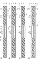
以下、本発明の第1実施形態を図1〜図10に基づいて説明する。本実施形態の回路基板10は、図1の平面図に示されているように、例えば、外縁部に沿った枠状の捨て領域R1を有し、その捨て領域R1の内側が正方形の複数の製品領域R2に区画されている。図2には、1つの製品領域R2が拡大して示され、その製品領域R2を対角線に沿って切断した回路基板10の断面構造が図3に拡大して示されている。
[First Embodiment]
Hereinafter, a first embodiment of the present invention will be described with reference to FIGS. As shown in the plan view of FIG. 1, the
図3に示すように、回路基板10は、コア基板11の表裏の両面にビルドアップ層20,20を有する構造になっている。コア基板11は、絶縁性部材で構成されている。コア基板11の表側の面であるF面11Fと、コア基板11の裏側の面であるS面11Sとには、導体回路層12がそれぞれ形成されている。また、コア基板11には、キャビティ16と複数の導電用貫通孔14が形成されている。
As shown in FIG. 3, the
導電用貫通孔14は、コア基板11のF面11F及びS面11Sの両面からそれぞれ穿孔しかつ奥側に向かって徐々に縮径したテーパー孔14A,14Aの小径側端部を互いに連通させた中間括れ形状をなしている。これに対し、キャビティ16は、直方体状の空間を有する形状になっている。
The through-holes for
各導電用貫通孔14内にはめっきが充填されて複数のスルーホール導電導体15がそれぞれ形成され、それらスルーホール導電導体15によってF面11Fの導体回路層12とS面11Sの導体回路層12との間が接続されている。
A plurality of through-hole
キャビティ16には、電子部品45と金属ブロック17とを重ね合わせてなる複合部品46が収容されている。金属ブロック17は、例えば銅製の偏平な直方体であって、金属ブロック17の平面形状は、キャビティ16の平面形状より一回り小さい四角形をなしている。また、金属ブロック17の厚さ、即ち、金属ブロック17の表裏の一方の面である第1主面17Fと、金属ブロック17の表裏の他方の面である第2主面17Sとの間の距離は、コア基板11の板厚より僅かに小さく、かつ、導体回路層12の厚さより大きくなっている。
The
また、金属ブロック17の第1主面17F及び第2主面17Sと、それら第1主面17F及び第2主面17Sの間の4つの側面17A(即ち、金属ブロック17の全ての外面)は、粗面になっている。具体的には、金属ブロック17を、酸液(例えば、硫酸と過酸化水素を主成分とした酸)に所定時間、漬けて表面を浸食させることで、金属ブロック17の表面の算術平均粗さRaは、0.1[μm]〜3.0[μm]になっている(JIS B 0601−1994の定義による)。
Further, the first
電子部品45は、例えば、半導体チップ30(例えば、CPU、メモリ)に、再配線層32を重ねてなる。半導体チップ30は、偏平な直方体状をなし、その平面形状は金属ブロック17より僅かに小さい四角形になっている。また、半導体チップ30は、表裏の一方の面で、本発明の端子面に相当する第1主面30Fのみに複数のパッド(図示しない)を有し、その第1主面30F上に再配線層32が重ねられている。再配線層32は、例えば、ポリイミドなどの絶縁性樹脂からなり、その内部に一方の面と他方の面を接続する配線がなされている。再配線層32内部の配線は、半導体チップ30側がより微細になっていて、半導体チップ30の第1主面30Fの複数のパッドは、再配線層32内部の配線によって、再配線層32の半導体チップ30と反対側の面に設けられ、第1主面30Fのパッドより大きい複数のパッド32Aに接続されている。即ち、再配線層32によって半導体チップ30のパッドのサイズ及び配置等が変更されている。そして、半導体チップ30のうち第1主面30Fと反対側の第2主面30Sが金属ブロック17の第1主面17Fに接着剤にて固定されている。なお、その接着剤としては、伝熱性に優れた導電性の接着剤が用いられている。
The
電子部品45と金属ブロック17とを合わせた複合部品46の全体の厚さは、コア基板11の板厚より僅かに大きくなっている。そして、電子部品45が、コア基板11のF面11Fから僅かに突出すると共に、金属ブロック17が、コア基板11のS面11Sから僅かに突出している。そして、電子部品45のパッドを有する接続面45F(即ち、再配線層32の一方の面)が、コア基板11のF面11Fにおける導体回路層12の最外面と略面一になる一方、金属ブロック17の第2主面17Sがコア基板11のS面11Sにおける導体回路層12の最外面と略面一になっている。また、金属ブロック17とキャビティ16の内面との間の隙間には、本発明に係る充填樹脂16Jが充填されている。
The total thickness of the
コア基板11のF面11F側のビルドアップ層20も、S面11S側のビルドアップ層20も共に、コア基板11側から順番に、第1絶縁樹脂層21、第1導体層22、第2絶縁樹脂層23、第2導体層24を積層してなり、第2導体層24上には、ソルダーレジスト層25が積層されている。また、第1絶縁樹脂層21及び第2絶縁樹脂層23には、それぞれ複数のビアホール21H,23Hが形成され、それらビアホール21H,23Hは、共にコア基板11側に向かって徐々に縮径したテーパー状になっている。さらに、これらビアホール21H,23H内にめっきが充填されて複数のビア導体21D,23Dが形成されている。そして、第1絶縁樹脂層21のビア導体21Dによって、導体回路層12と第1導体層22との間及び、金属ブロック17と第1導体層22との間及び、電子部品45と第1導体層22との間が接続され、第2絶縁樹脂層23のビア導体23Dによって、第1導体層22と第2導体層24の間が接続されている。また、ソルダーレジスト層25には、複数のパッド用孔が形成され、第2導体層24の一部がパッド用孔内に位置してパッド26になっている。
Both the build-up
コア基板11のF面11F上のビルドアップ層20の最外面である回路基板10のF面10Fにおいては、複数のパッド26が、製品領域R2の外縁部に沿って2列に並べられた大パッド26A群と、それら大パッド26A群に囲まれた内側の領域に縦横複数列に並べられた小パッド26C群とから構成されている。そして、例えば、図2に示すように、小パッド26C群における周囲一列の小パッド26Cを除いた四角形のエリアの真下となる位置に複合部品46が配置されている。また、図3に示すように、所定数の小パッド26Cが4つのビア導体21D,23Dを介して複合部品46の電子部品45に接続されている。これに対し、コア基板11のS面11S上のビルドアップ層20の最外面である回路基板10のS面10Sでは、小パッド26Cより大きな3つの中パッド26Bが本発明に係る基板接続部を構成し、所定の中パッド26Bがビア導体21D,23Dを介して複合部品46の金属ブロック17に接続されている。
On the
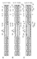
本実施形態の回路基板10は、以下のようにして製造される。
(1)図4(A)に示すように、コア基板11としてエポキシ樹脂又はBT(ビスマレイミドトリアジン)樹脂とガラスクロスなどの補強材からなる絶縁性基材11Kの表裏の両面に、銅箔11Cがラミネートされているものが用意される。
The
(1) As shown in FIG. 4A,
(2)図4(B)に示すように、コア基板11にF面11F側から例えばCO2レーザが照射されて導電用貫通孔14(図3参照)を形成するためのテーパー孔14Aが穿孔される。
(2) As shown in FIG. 4B, the
(3)図4(C)に示すように、コア基板11のS面11Sのうち前述したF面11F側のテーパー孔14Aの真裏となる位置にCO2レーザが照射されてテーパー孔14Aが穿孔され、それらテーパー孔14A,14Aから導電用貫通孔14が形成される。
(3) As shown in FIG. 4C, the
(4)無電解めっき処理が行われ、銅箔11C上と導電用貫通孔14の内面に無電解めっき膜(図示せず)が形成される。
(4) An electroless plating process is performed, and an electroless plating film (not shown) is formed on the
(5)図4(D)に示すように、銅箔11C上の無電解めっき膜上に、所定パターンのめっきレジスト33が形成される。
(5) As shown in FIG. 4D, a predetermined pattern of plating resist 33 is formed on the electroless plating film on the
(6)電解めっき処理が行われ、図5(A)に示すように、電解めっきが導電用貫通孔14内に充填されてスルーホール導電導体15が形成されると共に、銅箔11C上の無電解めっき膜(図示せず)のうちめっきレジスト33から露出している部分に電解めっき膜34が形成される。
(6) An electrolytic plating process is performed, and as shown in FIG. 5A, the electrolytic plating is filled in the conductive through
(7)めっきレジスト33が剥離されると共に、めっきレジスト33の下方の無電解めっき膜(図示せず)及び銅箔11Cが除去され、図5(B)に示すように、残された電解めっき膜34、無電解めっき膜及び銅箔11Cにより、コア基板11のF面11F上に導体回路層12が形成されると共に、コア基板11のS面11S上に導体回路層12が形成される。そして、F面11Fの導体回路層12とS面11Sの導体回路層12とがスルーホール導電導体15によって接続された状態になる。
(7) The plating resist 33 is peeled off, and the electroless plating film (not shown) and the
(8)図5(C)に示すように、コア基板11に、ルーター又はCO2レーザによってキャビティ16が形成される。
(8) As shown in FIG. 5C, the
(9)図5(D)に示すように、キャビティ16が塞がれるように、PETフィルムからなるテープ90がコア基板11のS面11S上に張り付けられる。
(9) As shown in FIG. 5D, a
(10)金属ブロック17が用意される。金属ブロック17は、銅の板材又は銅の角材を切断して形成され、耐酸性のメッシュ構造の容器に収容された状態で、貯留槽に貯留されている酸液(例えば、例えば、硫酸と過酸化水素を主成分とした酸)に所定時間浸された後、水洗される。これにより、金属ブロック17の表面全体が粗面になる。
(11)電子部品45が用意され、各電子部品45のうちパッドを有しない背面45Sが金属ブロック17の第1主面17Fに接着剤によって貼り付けられる。
(10) A
(11) The
(12)図6(A)に示すように、複合部品46がマウンター(図示せず)によってキャビティ16に収められる。このとき、複合部品46の電子部品45がコア基板11のF面11F側に配置され、金属ブロック17がコア基板11のS面11S側に配置される。
(12) As shown in FIG. 6A, the
(13)図6(B)に示すように、コア基板11のF面11F上の導体回路層12上に、第1絶縁樹脂層21としてのプリプレグ(心材を樹脂含浸してなるBステージの樹脂シート)と銅箔37が積層されてから、加熱プレスされる。その際、コア基板11のF面11Fの導体回路層12,12同士の間がプリプレグにて埋められ、プリプレグから染み出た熱硬化性樹脂がキャビティ16の内面と複合部品46との隙間に充填される。
(13) As shown in FIG. 6 (B), a prepreg as a first insulating resin layer 21 (B-stage resin formed by impregnating a core material with resin) on the
(14)図6(C)に示すように、テープ90を除去する。
(15)図6(D)に示すように、コア基板11のS面11S上の導体回路層12上に第1絶縁樹脂層21としてのプリプレグと銅箔37が積層されてから、加熱プレスされる。その際、コア基板11のS面11Sの導体回路層12,12同士の間がプリプレグにて埋められ、プリプレグから染み出た熱硬化性樹脂がキャビティ16の内面と複合部品46との隙間に充填される。また、コア基板11のF面11F及びS面11Sのプリプレグから染み出てキャビティ16の内面と複合部品46との隙間に充填された熱硬化性樹脂によって前述の充填樹脂16Jが形成される。
(14) As shown in FIG. 6C, the
(15) As shown in FIG. 6D, the prepreg as the first insulating
なお、第1絶縁樹脂層21としてプリプレグの代わりに心材を含まない樹脂フィルムを用いてもよい。その場合は、銅箔を積層することなく、樹脂フィルムの表面に、直接、セミアディティブ法で導体回路層を形成することができる。
A resin film that does not include a core material may be used as the first insulating
(16)図7(A)に示すように、上記したプリプレグによって形成されたコア基板11の表裏の両側の第1絶縁樹脂層21,21にCO2レーザが照射されて、複数のビアホール21Hが形成される。ここで、コア基板11のF面11F側に形成される複数のビアホール21Hは、一部のビアホール21Hがコア基板11のF面11Fの導体回路層12上に配置され、別の一部のビアホール21Hが電子部品45のパッド32A上に配置される。
(16) As shown in FIG. 7A, the first insulating resin layers 21 and 21 on both sides of the
また、コア基板11のS面11S側に形成される複数のビアホール21Hは、一部のビアホール21Hがコア基板11のS面11Sの導体回路層12上に配置され、別の一部のビアホール21Hが金属ブロック17上に配置される。なお、金属ブロック17上にビアホール21Hを形成する際に、ビアホール21Hの奥側に位置する金属ブロック17の粗面の凹凸はレーザ光照射または、照射後のデスミア処理で排除されてもよい。
In addition, a plurality of via
(17)無電解めっき処理が行われ、第1絶縁樹脂層21,21上と、ビアホール21H,21H内とに無電解めっき膜(図示せず)が形成される。
(17) An electroless plating process is performed to form an electroless plating film (not shown) on the first insulating resin layers 21 and 21 and in the via
(18)図7(B)に示すように、銅箔37上の無電解めっき膜上に、所定パターンのめっきレジスト40が形成される。
(18) As shown in FIG. 7B, a predetermined pattern of plating resist 40 is formed on the electroless plating film on the
(19)電解めっき処理が行われ、図7(C)に示すように、めっきがビアホール21H,21H内に充填されてビア導体21D,21Dが形成され、さらには、第1絶縁樹脂層21,21上の無電解めっき膜(図示せず)のうちめっきレジスト40から露出している部分に電解めっき膜39,39が形成される。
(19) The electrolytic plating process is performed, and as shown in FIG. 7C, the plating is filled in the via
(20)めっきレジスト40が剥離されると共に、めっきレジスト40の下方の無電解めっき膜(図示せず)及び銅箔37が除去され、図8(A)に示すように、残された電解めっき膜39、無電解めっき膜及び銅箔37により、コア基板11の表裏の各第1絶縁樹脂層21上に第1導体層22が形成される。そして、コア基板11の表裏の各第1導体層22の一部と導体回路層12とがビア導体21Dによって接続されると共に、コア基板11のF面11F側の第1導体層22の他の一部と電子部品45のパッド32Aとがビア導体21Dによって接続され、さらに、コア基板11のS面11S側の第1導体層22の他の一部と金属ブロック17のパッドとがビア導体21Dによって接続された状態になる。
(20) While the plating resist 40 is peeled off, the electroless plating film (not shown) and the
(21)上記した(13)〜(20)と同様の処理により、図8(B)に示すように、コア基板11の表裏の各第1導体層22上に第2絶縁樹脂層23と第2導体層24とが形成されて、各第2導体層24の一部と第1導体層22とがビア導体23Dによって接続された状態になる。
(21) Through the same processing as the above (13) to (20), as shown in FIG. 8B, the second insulating
(22)図8(C)に示すように、コア基板11の表裏の各第2導体層24上にソルダーレジスト層25,25が積層される。
(22) As shown in FIG. 8C, solder resist
(23)図9に示すように、コア基板11の表裏のソルダーレジスト層25,25の所定箇所にテーパー状のパッド用孔が形成され、コア基板11の表裏の各第2導体層24のうちパッド用孔から露出した部分がパッド26になる。
(23) As shown in FIG. 9, tapered pad holes are formed at predetermined positions of the solder resist
(24)パッド26上に、ニッケル層、パラジウム層、金層の順に積層されて図3に示した金属膜41が形成される。以上で回路基板10が完成する。
(24) On the
本実施形態の回路基板10の構造及び製造方法に関する説明は以上である。次に回路基板10の作用効果を、回路基板10の使用例と共に説明する。本実施形態の回路基板10は、例えば、以下のようにして使用される。即ち、図10に示すように、回路基板10の有する前述の大、中、小のパッド26A,26B,26C上に、それら各パッドの大きさに合った大、中、小の半田バンプ27A,27B,27Cが形成される。そして、例えば、回路基板10のF面10Fの小パッド群と同様に配置されたパッド群を下面に有するCPU80が、各製品領域R2の小半田バンプ27C群上に搭載されて半田付けされて、第1パッケージ基板10Pが形成される。このときCPU80と電子部品45とが、ビア導体21D,23Dを介して接続される。
This completes the description of the structure and manufacturing method of the
次いで、メモリ81を回路基板82のF面82Fに実装してなる第2パッケージ基板82Pが、CPU80の上方から第1パッケージ基板10P上に配されて、その第2パッケージ基板82Pにおける回路基板82のS面82Sに備えるパッドに第1パッケージ基板10Pにおける回路基板10の大半田バンプ27Aが半田付けされてPoP83(Package on Package83)が形成される。なお、PoP83における回路基板10,82の間には図示しない樹脂が充填される。
Next, a
次いで、PoP83がマザーボード84上に配されて、そのマザーボード84が有するパッド群にPoP83における回路基板10の中半田バンプ27Bが半田付けされる。このとき、マザーボード84が有する例えばグランド用のパッドが回路基板10のうち金属ブロック17に接続されているパッド26と半田付けされる。なお、マザーボード84が放熱専用のパッドを有している場合には、それら放熱専用のパッドと回路基板10の金属ブロック17とが、ビア導体21D,23Dで接続されてもよい。
Next, the PoP 83 is disposed on the
さて、PoP83が使用されると、CPU80及び電子部品45が共に発熱する。すると、電子部品45の熱が金属ブロック17に伝わり、回路基板10のS面10S側のビア導体21D,23Dを介して金属ブロック17からマザーボード84へと放熱される。これにより、電子部品45の温度上昇が抑えられる。また、これによりCPU80より電子部品45の温度が低くなると、CPU80の熱が回路基板10のF面10F側のビア導体21D,23Dを介して電子部品45、金属ブロック17へと伝わり、回路基板10のS面10S側のビア導体21D,23Dを介してマザーボード84へと放熱される。これにより、回路基板10に実装されているCPU80の温度上昇も抑えることができる。
When the PoP 83 is used, both the
また、回路基板10においては金属ブロック17の熱伸縮率が、第1絶縁樹脂層21や電子部品45等の他の部位の熱収縮率に比べて大きくなり得るが、金属ブロック17の外面全体が粗面になっていて接着剤や充填樹脂16Jにより他の部位に接続されているので、金属ブロック17と他の部位との剥離を抑えることができ、回路基板10における金属ブロック17の固定が安定する。また、金属ブロック17の外面を粗面にすることで、接着剤や充填樹脂16Jとの接触面積が増し、伝熱効率が上がる。
In the
[第2実施形態]
前記第1実施形態の回路基板10では、コア基板11に内蔵された複合部品46の真上に複合部品46の電子部品45と接続された別の電子部品(CPU80)が実装されていたが、複合部品の真上に別の電子部品が実装されていなくてもよい。本実施形態の回路基板50を使用した複合基板85を図11に示す。本実施形態では、コア基板11Vに形成されたキャビティ16Vに、電子部品(CPU80V)と金属ブロック17Vとからなる複合部品47が収容されている。そして、CPU80Vの端子面80Tの各パッドにビア導体21Dが接続されている。
[Second Embodiment]
In the
本実施形態の回路基板50の製造方法は、コア基板11Vへの複合部品47の収容方法が前記第1実施形態と異なる。具体的には、コア基板11Vにキャビティ16Vを形成し、コア基板11VのS面にテープ90を張り付けた後、まず、粗化した金属ブロック17Vのみをマウンターでキャビティ16Vに収める。次いで、キャビティ16Vに収容された金属ブロック17Vに接着フィルムを貼り付けて接着層86を形成する。次いで、端子面80Tと反対側の面を金属ブロック17V側にしたCPU80Vをマウンターでキャビティ16Vに収め、加圧して接着する。このようにして、CPU80Vと金属ブロック17Vとを接着してなる複合部品47がキャビティ16Vに収容される。なお、接着層86の形成は、例えば、接着剤をスプレーで塗布するなど異なる方法で行ってもよい。また、接着方法も、例えば、加熱によるものなど異なる方法によるものであってもよい。
The manufacturing method of the
本実施形態の回路基板50では、前記第1実施形態のように電子部品(CPU80)を回路基板上に実装した場合より、電子部品(CPU80V)が発する熱をS面50S側に逃がし易い。また、F面50F側に電子部品が突出しないので、複合基板85の厚みを減らすことができる。
In the
[他の実施形態]
本発明は、前記実施形態に限定されるものではなく、例えば、以下に説明するような実施形態も本発明の技術的範囲に含まれ、さらに、下記以外にも要旨を逸脱しない範囲内で種々変更して実施することができる。
[Other Embodiments]
The present invention is not limited to the above-described embodiment. For example, the embodiments described below are also included in the technical scope of the present invention, and various other than the following can be made without departing from the scope of the invention. It can be changed and implemented.
(1)前記実施形態の金属ブロック17,17Vは、銅の板材又は銅の角材を切断した後に表面を粗化していたが、切断前に粗化してもよい。その場合は、金属ブロック17,17Vの側面すべて、あるいは側面の一部の面は、粗化されていない状態になる。 (1) Although the metal blocks 17 and 17V of the said embodiment roughened the surface after cut | disconnecting a copper board | plate material or a copper square, you may roughen before cut | disconnecting. In that case, all of the side surfaces of the metal blocks 17 and 17V or a part of the side surfaces are not roughened.
(2)前記実施形態の金属ブロック17,17Vは、酸により表面の粗化を行っていたが、例えば粒子の吹き付けや、凹凸面の押し付けにより粗化を行ってもよい。 (2) The metal blocks 17 and 17V of the above embodiment have been roughened by acid, but may be roughened by, for example, spraying particles or pressing an uneven surface.
(3)前記実施形態の金属ブロック17,17Vには、回路基板10,50外のマザーボード84に熱を逃がすためのビア導体21D,23Dが接続されていたが、金属ブロック17,17Vにビア導体21D,23Dが接続されていなくてもよい。そのような構成であっても、金属ブロック17,17Vが電子部品(電子部品45、CPU80V)から熱を吸収することで、電子部品の急激な温度上昇を抑えることができ、また、金属ブロック17,17Vから回路基板10,50における電子部品の反対側に熱を逃がすことができる。
(3) Although the via
10,50 回路基板
11,11V コア基板
12 導体回路層
16,16V キャビティ
16J 充填樹脂
17,17V 金属ブロック
20 ビルドアップ層
21 第1絶縁樹脂層(絶縁樹脂層)
21D ビア導体
26A 大パッド(基板接続部)
26C 小パッド(電子部品実装部)
30F 第1主面30F(端子面)
45 電子部品
46,47 複合部品
80V CPU(電子部品)
80T 端子面
10, 50
21D via
26C small pad (electronic component mounting part)
30F 1st
45
80T terminal surface
Claims (12)
前記コア基板を貫通するキャビティと、
前記キャビティに収容される複合部品と、
前記コア基板の表面及び裏面にそれぞれ積層されて、前記キャビティを覆う絶縁樹脂層を含むビルドアップ層と、
前記キャビティと前記複合部品との隙間に充填される充填樹脂とを有する回路基板であって、
前記複合部品は、前記表面に向く側に端子面を有する電子部品と、前記端子面とは反対の面に重ねられる金属ブロックとからなる。 A core substrate;
A cavity penetrating the core substrate;
A composite part housed in the cavity;
A buildup layer including an insulating resin layer that is laminated on the front surface and the back surface of the core substrate and covers the cavity;
A circuit board having a filling resin filled in a gap between the cavity and the composite part,
The composite component includes an electronic component having a terminal surface on the side facing the surface and a metal block superimposed on a surface opposite to the terminal surface.
前記電子部品の端子及び前記金属ブロックには、前記ビルドアップ層に含まれるビア導体が接続されている。 The circuit board according to claim 1,
A via conductor included in the buildup layer is connected to the terminal of the electronic component and the metal block.
前記コア基板の表面及び裏面に導体回路層が積層されて、それら各導体回路層の上に前記ビルドアップ層が積層され、
前記電子部品のうち前記端子面及び、前記金属ブロックのうち前記電子部品との重ね合わせ面と反対側の面が、それぞれ前記導体回路層と前記ビルドアップ層との境界面に位置している。 The circuit board according to claim 1 or 2,
Conductor circuit layers are laminated on the front and back surfaces of the core substrate, and the build-up layer is laminated on each of the conductor circuit layers,
The terminal surface of the electronic component and the surface of the metal block opposite to the overlapping surface with the electronic component are located at the boundary surface between the conductor circuit layer and the buildup layer, respectively.
前記金属ブロックは、前記導体回路層よりも厚い。 The circuit board according to claim 3,
The metal block is thicker than the conductor circuit layer.
前記電子部品の前記金属ブロックとの重ね合わせ面よりも前記金属ブロックの前記電子部品との重ね合わせ面の方が広い。 A circuit board according to any one of claims 1 to 4,
The overlapping surface of the metal block with the electronic component is wider than the overlapping surface of the electronic component with the metal block.
前記電子部品と前記金属ブロックとが導電性接着剤で接着されている。 A circuit board according to any one of claims 1 to 5,
The electronic component and the metal block are bonded with a conductive adhesive.
前記金属ブロックにおける樹脂との接続面は、算術平均粗さが0.1[μm]〜3.0[μm]の粗面になっている。 A circuit board according to any one of claims 1 to 6,
The connection surface with the resin in the metal block is a rough surface having an arithmetic average roughness of 0.1 [μm] to 3.0 [μm].
前記複合部品のうち前記電子部品が前記表面側、前記金属ブロックが前記裏面側に配置され、
前記コア基板の表側に積層される前記ビルドアップ層の最外部のうち前記複合部品の真上となる位置には、他の電子部品が実装される電子部品実装部が設けられ、前記ビルドアップ層の最外部のうち前記電子部品実装部の周りには、前記他の電子部品の上から重ねられる他の回路基板が接続される基板接続部が設けられている。 A circuit board according to any one of claims 1 to 7,
Among the composite parts, the electronic parts are arranged on the front side, and the metal block is arranged on the back side,
An electronic component mounting portion on which another electronic component is mounted is provided at a position directly above the composite component among the outermost layers of the buildup layer stacked on the front side of the core substrate, and the buildup layer A board connection part to which another circuit board that is overlaid on the other electronic parts is connected is provided around the electronic part mounting part among the outermost parts.
前記金属ブロックは、グランド用配線に接続されている。 A circuit board according to any one of claims 1 to 8,
The metal block is connected to a ground wiring.
表裏の一方の面に端子面を有する電子部品と、前記端子面とは反対の面に重ねられる金属ブロックとからなる複合部品を前記キャビティに収容することと、
前記コア基板の表裏に前記キャビティ及び前記複合部品を覆うビルドアップ層を積層することと、
前記キャビティと前記複合部品との隙間に充填樹脂を充填すること、を含む回路基板の製造方法。 Forming a cavity in the core substrate;
Containing a composite component composed of an electronic component having a terminal surface on one side of the front and back and a metal block superimposed on a surface opposite to the terminal surface in the cavity;
Laminating a build-up layer covering the cavity and the composite part on the front and back of the core substrate;
Filling a gap between the cavity and the composite component with a filling resin.
前記複合部品を前記キャビティに収容する前に、前記複合部品を構成する前記電子部品と前記金属ブロックとを接着する。 In the manufacturing method of the circuit board according to claim 10,
Before the composite component is accommodated in the cavity, the electronic component constituting the composite component and the metal block are bonded.
前記複合部品を構成する前記電子部品及び前記金属ブロックのうち前記金属ブロックのみを前記キャビティに収容した後、前記電子部品を収容して、前記キャビティ内で前記電子部品と前記金属ブロックを接着して前記複合部品にする。 In the manufacturing method of the circuit board according to claim 10,
Of the electronic component and the metal block constituting the composite component, after housing only the metal block in the cavity, housing the electronic component, and bonding the electronic component and the metal block in the cavity The composite part is used.
Priority Applications (2)
| Application Number | Priority Date | Filing Date | Title |
|---|---|---|---|
| JP2014146770A JP2016025143A (en) | 2014-07-17 | 2014-07-17 | Circuit board and manufacturing method of the same |
| US14/802,139 US9955591B2 (en) | 2014-07-17 | 2015-07-17 | Circuit substrate and method for manufacturing the same |
Applications Claiming Priority (1)
| Application Number | Priority Date | Filing Date | Title |
|---|---|---|---|
| JP2014146770A JP2016025143A (en) | 2014-07-17 | 2014-07-17 | Circuit board and manufacturing method of the same |
Publications (1)
| Publication Number | Publication Date |
|---|---|
| JP2016025143A true JP2016025143A (en) | 2016-02-08 |
Family
ID=55075824
Family Applications (1)
| Application Number | Title | Priority Date | Filing Date |
|---|---|---|---|
| JP2014146770A Pending JP2016025143A (en) | 2014-07-17 | 2014-07-17 | Circuit board and manufacturing method of the same |
Country Status (2)
| Country | Link |
|---|---|
| US (1) | US9955591B2 (en) |
| JP (1) | JP2016025143A (en) |
Cited By (10)
| Publication number | Priority date | Publication date | Assignee | Title |
|---|---|---|---|---|
| KR20170033112A (en) * | 2015-09-16 | 2017-03-24 | 삼성전기주식회사 | Printed circuit board |
| US9852995B1 (en) | 2016-09-21 | 2017-12-26 | Kabushiki Kaisha Toshiba | Semiconductor device |
| JP2018074142A (en) * | 2016-10-25 | 2018-05-10 | 旭徳科技股▲ふん▼有限公司 | Package carrier and manufacturing method thereof |
| JP2019087731A (en) * | 2017-11-08 | 2019-06-06 | サムソン エレクトロ−メカニックス カンパニーリミテッド. | Fan-out semiconductor package |
| US10643919B2 (en) | 2017-11-08 | 2020-05-05 | Samsung Electronics Co., Ltd. | Fan-out semiconductor package |
| KR20200055555A (en) * | 2018-11-13 | 2020-05-21 | 삼성전기주식회사 | Package structure |
| JP2020174115A (en) * | 2019-04-10 | 2020-10-22 | 株式会社フジクラ | Multilayer circuit board |
| CN113013130A (en) * | 2019-12-20 | 2021-06-22 | 奥特斯科技(重庆)有限公司 | Component carrier with dual dielectric layers and method for manufacturing the same |
| CN115148687A (en) * | 2021-03-30 | 2022-10-04 | 株式会社电装 | Semiconductor devices with electrical components built into circuit boards |
| WO2025084247A1 (en) * | 2023-10-19 | 2025-04-24 | 株式会社デンソー | Semiconductor device |
Families Citing this family (16)
| Publication number | Priority date | Publication date | Assignee | Title |
|---|---|---|---|---|
| JP2016015432A (en) * | 2014-07-03 | 2016-01-28 | イビデン株式会社 | Circuit board and method of manufacturing the same |
| US10512153B2 (en) * | 2016-04-27 | 2019-12-17 | Mitsubishi Electric Corporation | High frequency circuit |
| CN106455320B (en) * | 2016-09-29 | 2019-02-15 | 北京航天时代光电科技有限公司 | A kind of anti-vibration reinforcement means of electronic component |
| KR102561987B1 (en) * | 2017-01-11 | 2023-07-31 | 삼성전기주식회사 | Semiconductor package and manufacturing method for the same |
| JP2019079902A (en) * | 2017-10-24 | 2019-05-23 | イビデン株式会社 | Printed wiring board |
| KR102492796B1 (en) * | 2018-01-29 | 2023-01-30 | 삼성전자주식회사 | Semiconductor package |
| EP3716321B1 (en) * | 2019-03-29 | 2025-01-29 | AT & S Austria Technologie & Systemtechnik Aktiengesellschaft | Component carrier with embedded semiconductor component and embedded highly conductive block which are mutually coupled |
| US12245377B2 (en) * | 2019-03-29 | 2025-03-04 | At&S Austria Technologie & Systemtechnik Aktiengesellschaft | Component carrier with embedded semiconductor component and embedded highly-conductive block which are mutually coupled |
| US11527462B2 (en) | 2019-12-13 | 2022-12-13 | International Business Machines Corporation | Circuit substrate with mixed pitch wiring |
| US11107771B2 (en) * | 2019-12-26 | 2021-08-31 | Taiwan Semiconductor Manufacturing Company, Ltd. | Segregated power and ground design for yield improvement |
| KR102766435B1 (en) * | 2020-02-17 | 2025-02-12 | 삼성전자주식회사 | Semiconductor package |
| EP3869923B1 (en) * | 2020-02-20 | 2025-01-08 | AT & S Austria Technologie & Systemtechnik Aktiengesellschaft | Cooling profile integration for embedded power systems |
| JP7567931B2 (en) * | 2020-11-19 | 2024-10-16 | 日本電信電話株式会社 | Method for fabricating integrated electronic components |
| TWI752820B (en) * | 2021-02-08 | 2022-01-11 | 欣興電子股份有限公司 | Circuit board structure and manufacturing method thereof |
| US11967591B2 (en) * | 2021-08-06 | 2024-04-23 | Taiwan Semiconductor Manufacturing Co., Ltd. | Info packages including thermal dissipation blocks |
| CN121058353A (en) * | 2023-07-07 | 2025-12-02 | 微芯片技术卡尔迪科特有限公司 | Substrate with embedded conductive coin |
Family Cites Families (5)
| Publication number | Priority date | Publication date | Assignee | Title |
|---|---|---|---|---|
| US5642261A (en) * | 1993-12-20 | 1997-06-24 | Sgs-Thomson Microelectronics, Inc. | Ball-grid-array integrated circuit package with solder-connected thermal conductor |
| TWI400998B (en) * | 2010-08-20 | 2013-07-01 | 南亞電路板股份有限公司 | Printed circuit board and method of manufacturing same |
| JP2013038374A (en) | 2011-01-20 | 2013-02-21 | Ibiden Co Ltd | Wiring board and manufacturing method of the same |
| KR20130014122A (en) * | 2011-07-29 | 2013-02-07 | 삼성전기주식회사 | Electronic components embedded pcb and method for manufacturing thereof |
| TWI489918B (en) * | 2012-11-23 | 2015-06-21 | 旭德科技股份有限公司 | Package carrier |
-
2014
- 2014-07-17 JP JP2014146770A patent/JP2016025143A/en active Pending
-
2015
- 2015-07-17 US US14/802,139 patent/US9955591B2/en active Active
Cited By (17)
| Publication number | Priority date | Publication date | Assignee | Title |
|---|---|---|---|---|
| KR20170033112A (en) * | 2015-09-16 | 2017-03-24 | 삼성전기주식회사 | Printed circuit board |
| KR102435128B1 (en) | 2015-09-16 | 2022-08-24 | 삼성전기주식회사 | Printed circuit board |
| US9852995B1 (en) | 2016-09-21 | 2017-12-26 | Kabushiki Kaisha Toshiba | Semiconductor device |
| US10424542B2 (en) | 2016-09-21 | 2019-09-24 | Kabushiki Kaisha Toshiba | Semiconductor device |
| JP2018074142A (en) * | 2016-10-25 | 2018-05-10 | 旭徳科技股▲ふん▼有限公司 | Package carrier and manufacturing method thereof |
| US10177067B2 (en) | 2016-10-25 | 2019-01-08 | Subtron Technology Co., Ltd. | Manufacturing method of package carrier |
| TWI695465B (en) * | 2017-11-08 | 2020-06-01 | 南韓商三星電子股份有限公司 | Fan-out semiconductor package |
| US10643919B2 (en) | 2017-11-08 | 2020-05-05 | Samsung Electronics Co., Ltd. | Fan-out semiconductor package |
| JP2019087731A (en) * | 2017-11-08 | 2019-06-06 | サムソン エレクトロ−メカニックス カンパニーリミテッド. | Fan-out semiconductor package |
| KR20200055555A (en) * | 2018-11-13 | 2020-05-21 | 삼성전기주식회사 | Package structure |
| KR102561946B1 (en) | 2018-11-13 | 2023-08-01 | 삼성전기주식회사 | Package structure |
| JP2020174115A (en) * | 2019-04-10 | 2020-10-22 | 株式会社フジクラ | Multilayer circuit board |
| CN113013130A (en) * | 2019-12-20 | 2021-06-22 | 奥特斯科技(重庆)有限公司 | Component carrier with dual dielectric layers and method for manufacturing the same |
| US12207399B2 (en) | 2019-12-20 | 2025-01-21 | AT&S (Chongqing) Company Limited | Component carrier having a double dielectric layer and method of manufacturing the same |
| CN115148687A (en) * | 2021-03-30 | 2022-10-04 | 株式会社电装 | Semiconductor devices with electrical components built into circuit boards |
| JP2022154932A (en) * | 2021-03-30 | 2022-10-13 | 株式会社デンソー | Semiconductor device with electric component in circuit board |
| WO2025084247A1 (en) * | 2023-10-19 | 2025-04-24 | 株式会社デンソー | Semiconductor device |
Also Published As
| Publication number | Publication date |
|---|---|
| US9955591B2 (en) | 2018-04-24 |
| US20160021753A1 (en) | 2016-01-21 |
Similar Documents
| Publication | Publication Date | Title |
|---|---|---|
| JP2016025143A (en) | Circuit board and manufacturing method of the same | |
| US9893016B2 (en) | Multilayer wiring board having wiring structure for mounting multiple electronic components and method for manufacturing the same | |
| JP2016015432A (en) | Circuit board and method of manufacturing the same | |
| JP2016015433A (en) | Circuit board and method of manufacturing the same | |
| JP2016096297A (en) | Metal block built-in wiring board and method of manufacturing the same | |
| JP5873152B1 (en) | Wiring board | |
| JP2015211204A (en) | Circuit board and manufacturing method thereof | |
| US10306759B2 (en) | Wiring substrate | |
| US9613893B2 (en) | Wiring substrate and method for manufacturing the same | |
| JP2014229698A (en) | Wiring board and manufacturing method therefor | |
| JP2016063130A (en) | Printed wiring board and semiconductor package | |
| JP2015028986A (en) | Printed wiring board and printed wiring board manufacturing method | |
| JP2015211194A (en) | Printed wiring board, semiconductor package, and method for manufacturing printed wiring board | |
| JP2015170770A (en) | Printed wiring board | |
| JP2016149475A (en) | Circuit board and manufacturing method thereof | |
| JP2016171118A (en) | Circuit board and manufacturing method thereof | |
| JP2015225895A (en) | Printed wiring board, semiconductor package, and method for manufacturing printed wiring board | |
| JP2013140955A (en) | Printed circuit board with built-in component and manufacturing method thereof | |
| JP2016171119A (en) | Circuit board and method of manufacturing the same | |
| JP6378616B2 (en) | Printed wiring board with built-in electronic components | |
| JP2013115136A (en) | Substrate with built-in electronic components and manufacturing method of the same | |
| JP2017174953A (en) | Printed wiring board and manufacturing method of printed wiring board | |
| JP2016127148A (en) | Wiring board manufacturing method | |
| JP2017069474A (en) | Circuit board and manufacturing method therefor | |
| JP2013030808A (en) | Temporary substrate for wiring board manufacturing and manufacturing method of the same |