JP2015513067A - Photoconductive device having a plasmon electrode - Google Patents
Photoconductive device having a plasmon electrode Download PDFInfo
- Publication number
- JP2015513067A JP2015513067A JP2014553536A JP2014553536A JP2015513067A JP 2015513067 A JP2015513067 A JP 2015513067A JP 2014553536 A JP2014553536 A JP 2014553536A JP 2014553536 A JP2014553536 A JP 2014553536A JP 2015513067 A JP2015513067 A JP 2015513067A
- Authority
- JP
- Japan
- Prior art keywords
- plasmon
- photoconductive
- photoconductive device
- antenna
- semiconductor substrate
- Prior art date
- Legal status (The legal status is an assumption and is not a legal conclusion. Google has not performed a legal analysis and makes no representation as to the accuracy of the status listed.)
- Granted
Links
Images


Classifications
-
- G—PHYSICS
- G01—MEASURING; TESTING
- G01J—MEASUREMENT OF INTENSITY, VELOCITY, SPECTRAL CONTENT, POLARISATION, PHASE OR PULSE CHARACTERISTICS OF INFRARED, VISIBLE OR ULTRAVIOLET LIGHT; COLORIMETRY; RADIATION PYROMETRY
- G01J3/00—Spectrometry; Spectrophotometry; Monochromators; Measuring colours
- G01J3/02—Details
- G01J3/10—Arrangements of light sources specially adapted for spectrometry or colorimetry
- G01J3/108—Arrangements of light sources specially adapted for spectrometry or colorimetry for measurement in the infrared range
-
- H—ELECTRICITY
- H10—SEMICONDUCTOR DEVICES; ELECTRIC SOLID-STATE DEVICES NOT OTHERWISE PROVIDED FOR
- H10F—INORGANIC SEMICONDUCTOR DEVICES SENSITIVE TO INFRARED RADIATION, LIGHT, ELECTROMAGNETIC RADIATION OF SHORTER WAVELENGTH OR CORPUSCULAR RADIATION
- H10F30/00—Individual radiation-sensitive semiconductor devices in which radiation controls the flow of current through the devices, e.g. photodetectors
- H10F30/10—Individual radiation-sensitive semiconductor devices in which radiation controls the flow of current through the devices, e.g. photodetectors the devices being sensitive to infrared radiation, visible or ultraviolet radiation, and having no potential barriers, e.g. photoresistors
-
- H—ELECTRICITY
- H10—SEMICONDUCTOR DEVICES; ELECTRIC SOLID-STATE DEVICES NOT OTHERWISE PROVIDED FOR
- H10F—INORGANIC SEMICONDUCTOR DEVICES SENSITIVE TO INFRARED RADIATION, LIGHT, ELECTROMAGNETIC RADIATION OF SHORTER WAVELENGTH OR CORPUSCULAR RADIATION
- H10F77/00—Constructional details of devices covered by this subclass
- H10F77/10—Semiconductor bodies
- H10F77/14—Shape of semiconductor bodies; Shapes, relative sizes or dispositions of semiconductor regions within semiconductor bodies
- H10F77/143—Shape of semiconductor bodies; Shapes, relative sizes or dispositions of semiconductor regions within semiconductor bodies comprising quantum structures
-
- H—ELECTRICITY
- H10—SEMICONDUCTOR DEVICES; ELECTRIC SOLID-STATE DEVICES NOT OTHERWISE PROVIDED FOR
- H10F—INORGANIC SEMICONDUCTOR DEVICES SENSITIVE TO INFRARED RADIATION, LIGHT, ELECTROMAGNETIC RADIATION OF SHORTER WAVELENGTH OR CORPUSCULAR RADIATION
- H10F77/00—Constructional details of devices covered by this subclass
- H10F77/20—Electrodes
-
- H—ELECTRICITY
- H10—SEMICONDUCTOR DEVICES; ELECTRIC SOLID-STATE DEVICES NOT OTHERWISE PROVIDED FOR
- H10F—INORGANIC SEMICONDUCTOR DEVICES SENSITIVE TO INFRARED RADIATION, LIGHT, ELECTROMAGNETIC RADIATION OF SHORTER WAVELENGTH OR CORPUSCULAR RADIATION
- H10F77/00—Constructional details of devices covered by this subclass
- H10F77/40—Optical elements or arrangements
- H10F77/413—Optical elements or arrangements directly associated or integrated with the devices, e.g. back reflectors
-
- H—ELECTRICITY
- H10—SEMICONDUCTOR DEVICES; ELECTRIC SOLID-STATE DEVICES NOT OTHERWISE PROVIDED FOR
- H10H—INORGANIC LIGHT-EMITTING SEMICONDUCTOR DEVICES HAVING POTENTIAL BARRIERS
- H10H20/00—Individual inorganic light-emitting semiconductor devices having potential barriers, e.g. light-emitting diodes [LED]
- H10H20/80—Constructional details
- H10H20/81—Bodies
- H10H20/811—Bodies having quantum effect structures or superlattices, e.g. tunnel junctions
-
- H—ELECTRICITY
- H10—SEMICONDUCTOR DEVICES; ELECTRIC SOLID-STATE DEVICES NOT OTHERWISE PROVIDED FOR
- H10H—INORGANIC LIGHT-EMITTING SEMICONDUCTOR DEVICES HAVING POTENTIAL BARRIERS
- H10H20/00—Individual inorganic light-emitting semiconductor devices having potential barriers, e.g. light-emitting diodes [LED]
- H10H20/80—Constructional details
- H10H20/83—Electrodes
- H10H20/831—Electrodes characterised by their shape
Landscapes
- Physics & Mathematics (AREA)
- Spectroscopy & Molecular Physics (AREA)
- General Physics & Mathematics (AREA)
- Optical Modulation, Optical Deflection, Nonlinear Optics, Optical Demodulation, Optical Logic Elements (AREA)
- Investigating Or Analysing Materials By Optical Means (AREA)
- Photometry And Measurement Of Optical Pulse Characteristics (AREA)
Abstract
光伝導装置は、半導体基板と、アンテナ組立体と、1つ以上のプラズモン接触電極を有する光伝導組立体とを含む。光伝導組立体は、半導体基板の光吸収領域へのポンプ吸収をプラズモニックに増強することによって光伝導装置の量子効率を向上させるように、半導体基板上に配置されたプラズモン接触電極を備えることができる。例示的な一実施形態において、光伝導装置は、光伝導源として配置され、通信ポンプ波長(たとえば、1.0〜1.6μm)でポンプされ、テラヘルツ(THz)周波数領域においてミリワット級の出力を生成する。The photoconductive device includes a semiconductor substrate, an antenna assembly, and a photoconductive assembly having one or more plasmon contact electrodes. The photoconductive assembly may comprise a plasmon contact electrode disposed on the semiconductor substrate to improve the quantum efficiency of the photoconductive device by plasmonically enhancing pump absorption into the light absorption region of the semiconductor substrate. it can. In an exemplary embodiment, the photoconductive device is arranged as a photoconductive source, pumped at a communication pump wavelength (eg, 1.0-1.6 μm), and has a milliwatt output in the terahertz (THz) frequency domain. Generate.
Description
連邦政府による資金提供を受けた研究の陳述
本発明は、助成番号N66001−10−1−4027における海軍/SPAWARからの政府支援、助成番号W911NF−12−1−0253における陸軍研究室からの政府支援、助成番号N00014−11−1−0856における海軍研究事務所からの政府支援、助成番号EECCS1054454における国立科学財団からの政府支援、およびN00014−11−1−0096における海軍研究事務所からの政府支援によって行われた。連邦政府は、本発明における一定の権利を所有する。
Statement of research funded by the federal government The present invention relates to government support from Navy / SPAWAR at grant number N66001-10-1-4027, government support from Army Lab at grant number W911NF-12-1-0253 Government support from the Navy Research Office at Grant Number N00014-11-1-0856, Government Support from the National Science Foundation at Grant Number EECCS 10544454, and Government Support from the Navy Research Office at N00014-11-10096 It was conducted. The federal government owns certain rights in the invention.
技術分野
本発明は、一般的には光伝導装置に関し、より具体的には、量子効率を改善するためにプラズモン電極を用いる、テラヘルツ(THz)波を発するまたは検出する光伝導装置に関する。
TECHNICAL FIELD The present invention relates generally to photoconductive devices, and more specifically to photoconductive devices that emit or detect terahertz (THz) waves that use plasmon electrodes to improve quantum efficiency.
発明の背景
テラヘルツ(THz)波は、多数の独特な性能および性質を有する。いくつかの例として、テラヘルツ波は、化学同定、材料特性測定、生物学的検知、および医療撮像において有用である。テラヘルツ時間領域分光法(THz−TDS)は、非常に短いパルスのTHz放射を用いて材料の異なる性質をプローブまたは分析する分光技術であり、材料がTHz放射の振幅および位相の両方に与える影響を感知できる。THz−TDSシステムは商業使用において多大な可能性があるが、これまでその使用は、たとえば低出力、効率の悪さ、高コスト、熱破壊、複雑さ、および既存のテラヘルツ波源が巨大であるなどの特定の欠点によって妨げられている。
BACKGROUND OF THE INVENTION Terahertz (THz) waves have a number of unique performances and properties. As some examples, terahertz waves are useful in chemical identification, material property measurement, biological sensing, and medical imaging. Terahertz time-domain spectroscopy (THz-TDS) is a spectroscopic technique that uses very short pulses of THz radiation to probe or analyze different properties of a material and how the material affects both the amplitude and phase of THz radiation. It can be perceived. THz-TDS systems have tremendous potential in commercial use, but to date their use has been, for example, low power, inefficient, high cost, thermal destruction, complexity, and huge existing terahertz sources It is hampered by certain drawbacks.
たとえば、ほとんどの既存のテラヘルツ(THz)分光計は、軍事目的および商業目的の化学的検出および/または特性測定に広く使用されていない。これは、主に、これらの装置、特に携帯用装置の実用可能性を妨げる上述した欠点のためである。いくつか例を挙げると、いくつかの研究は、可干渉性テラヘルツ波源、固体テラヘルツ波源、量子カスケードレーザ(QCL)および低いテラヘルツ周波数に変換するための非線形光学技術を利用する周波数領域テラヘルツ分光計の分野において行われている。しかしながら、これらの手法の各々は、それぞれ自身の欠点を有する。比較的小型でかつ通常の動作条件下で、テラヘルツ(THz)または近くの周波数の広い周波数領域にわたって適切な出力パワーおよび効率を提供する手法を見出すことは、難題である。 For example, most existing terahertz (THz) spectrometers are not widely used for military and commercial chemical detection and / or characterization. This is mainly due to the above-mentioned drawbacks that impede the feasibility of these devices, especially portable devices. To name a few examples, some studies have shown that coherent terahertz sources, solid state terahertz sources, quantum cascade lasers (QCL) and frequency domain terahertz spectrometers that use nonlinear optical techniques to convert to lower terahertz frequencies. It is done in the field. However, each of these approaches has its own drawbacks. Finding a technique that provides adequate output power and efficiency over a wide frequency range of terahertz (THz) or near frequencies under relatively small and normal operating conditions is a challenge.
発明の概要
一局面によれば、テラヘルツ(THz)放射を発するまたは検出するための光伝導装置が提供される。光伝導装置は、半導体基板と、半導体基板上に作製されたアンテナ組立体と、半導体基板上に作製され、アンテナ組立体に結合された光伝導体組立体とを備えることができる。光伝導体組立体は、1つ以上のプラズモン接触電極を含む。光伝導装置は、少なくとも1つの光源からの光入力を受光し、光伝導装置の量子効率を改善するためにプラズモン接触電極を用いる。
SUMMARY OF THE INVENTION According to one aspect, a photoconductive device for emitting or detecting terahertz (THz) radiation is provided. The photoconductive device can comprise a semiconductor substrate, an antenna assembly fabricated on the semiconductor substrate, and a photoconductor assembly fabricated on the semiconductor substrate and coupled to the antenna assembly. The photoconductor assembly includes one or more plasmon contact electrodes. The photoconductive device receives light input from at least one light source and uses plasmon contact electrodes to improve the quantum efficiency of the photoconductive device.
別の局面によれば、半導体基板と、アンテナ組立体と、1つ以上のプラズモン接触電極とを有する光伝導装置を動作させる方法が提供される。方法は、(a)半導体基板において光源からの光入力を受光するステップと、(b)プラズモン接触電極を用いて表面プラズモン波または表面波の励起を促進するステップとを備え、表面プラズモン波または表面波は、より多くの光入力が半導体基板に吸収されて半導体基板において光電流をもたらすように、光源からの光入力に影響を与え、さらに、(c)半導体基板における光電流の第1の部分が第1のアンテナ端子に向かってドリフトし、半導体基板における光電流の第2の部分が第2のアンテナ端子に向かってドリフトするように、アンテナ組立体に電圧を印加するステップと、(d)光電流の第1および第2の部分が供給されている第1および第2のアンテナ端子に応答して光伝導装置からテラヘルツ(THz)放射を発するステップとを備えることができる。 According to another aspect, a method of operating a photoconductive device having a semiconductor substrate, an antenna assembly, and one or more plasmon contact electrodes is provided. The method comprises the steps of: (a) receiving light input from a light source at a semiconductor substrate; and (b) promoting excitation of a surface plasmon wave or surface wave using a plasmon contact electrode. The wave affects the light input from the light source such that more light input is absorbed by the semiconductor substrate and results in a photocurrent at the semiconductor substrate, and (c) a first portion of the photocurrent at the semiconductor substrate. Applying a voltage to the antenna assembly such that drifts toward the first antenna terminal and a second portion of the photocurrent in the semiconductor substrate drifts toward the second antenna terminal; (d) A stage emitting terahertz (THz) radiation from the photoconductive device in response to the first and second antenna terminals to which the first and second portions of photocurrent are supplied. It can be and a flop.
別の局面によれば、半導体基板と、アンテナ組立体と、1つ以上のプラズモン接触電極とを有する光伝導装置を動作させる方法が提供される。方法は、(a)半導体基板において光源からの光入力を受光するステップと、(b)プラズモン接触電極を用いて表面プラズモン波または表面波の励起を促進するステップとを備え、表面プラズモン波または表面波は、より多くの光入力が半導体基板に吸収されて半導体基板において光電流をもたらすように、光源からの光入力に影響を与え、さらに、(c)アンテナ組立体を介して入射するテラヘルツ放射を受け取るステップを備え、前記入射するテラヘルツ放射はプラズモン接触電極の間にテラヘルツ電界を誘起し、さらに、(d)入射するテラヘルツ放射の大きさに比例する出力光電流を発生する誘起されたテラヘルツ電場の結果として、プラズモン接触電極に向かって光電流をドリフトさせるステップを備えることができる。 According to another aspect, a method of operating a photoconductive device having a semiconductor substrate, an antenna assembly, and one or more plasmon contact electrodes is provided. The method comprises the steps of: (a) receiving light input from a light source at a semiconductor substrate; and (b) promoting excitation of a surface plasmon wave or surface wave using a plasmon contact electrode. The wave affects the light input from the light source such that more light input is absorbed by the semiconductor substrate and results in a photocurrent at the semiconductor substrate, and (c) terahertz radiation incident through the antenna assembly. Wherein the incident terahertz radiation induces a terahertz electric field between the plasmon contact electrodes, and (d) an induced terahertz electric field that generates an output photocurrent proportional to the magnitude of the incident terahertz radiation. As a result, a step of drifting the photocurrent toward the plasmon contact electrode can be provided.
例示的な実施形態の詳細な説明
以下、添付図面と併せて、好ましい例示的な実施形態を説明する。図面において、同様の記号は、同様の構成要素を示す。
DETAILED DESCRIPTION OF EXEMPLARY EMBODIMENTS Preferred exemplary embodiments will now be described in conjunction with the accompanying drawings. In the drawings, like symbols indicate like components.
本願明細書に記載された光伝導性装置は、既存の光伝導装置のいくつかの性能限界に対処している。例示的な実施形態によれば、光伝導装置は、通信ポンプ波長(たとえば、1.0〜1.6μm)でポンプされる、高性能なプラズモン分布型光伝導テラヘルツ波源であってもよい。このようなテラヘルツ波源として、高出力、狭い線幅、可変周波数、小型かつコスト効率の高い光源が利用可能である。多数の分布型プラズモン接触電極を有する光伝導体組立体は、ポンプ結合効率を著しく高めるとともに、光生成キャリアの超高速収集を可能にし、かつ、高ポンプ出力で動作中において発生する可能性のあるキャリア遮蔽効果および熱破壊限界を緩和することができる。これによって、テラヘルツ波出力を現在利用可能なレベルよりも著しく高いレベルにすることができる。1つの例示的な実現例によれば、光伝導装置は、2つの市販レーザダイオードとエルビウム添加光ファイバ増幅器からの光入力を受光して、1THzの周波数領域においてミリワット級の出力を生成することができる周波数可変で小型かつ軽量なテラヘルツ(パルスまたは非パルス)放射源である。このような高出力かつ小型のテラヘルツ波源は、次世代材料、化学的および/または生物学的センサを含む数多くの潜在的な用途に対して有益であり得る。以下の説明は、テラヘルツ放射を発する光伝導波源を対象にしているが、理解すべきことは、本明細書の教示がテラヘルツ放射を発するのではなく、テラヘルツ放射を受け取る光伝導検出器にも同様に適用可能であることである。したがって、本明細書で使用された用語「光伝導装置」は、光伝導波源と光伝導検出器との両方を含み、一方または他方に限定されるものではない。 The photoconductive devices described herein address several performance limitations of existing photoconductive devices. According to an exemplary embodiment, the photoconductive device may be a high performance plasmon distributed photoconductive terahertz source pumped at a communication pump wavelength (eg, 1.0-1.6 μm). As such a terahertz wave source, a high-output, narrow line width, variable frequency, small and cost-effective light source can be used. A photoconductor assembly having a large number of distributed plasmon contact electrodes significantly increases pump coupling efficiency, enables ultrafast collection of photogenerated carriers, and may occur during operation at high pump power Carrier shielding effect and thermal destruction limit can be relaxed. This allows the terahertz wave output to be significantly higher than currently available levels. According to one exemplary implementation, the photoconductive device can receive light input from two commercially available laser diodes and an erbium-doped fiber amplifier and produce milliwatt-class output in the 1 THz frequency range. A terahertz (pulsed or non-pulsed) radiation source that is variable in frequency, small and lightweight. Such high power and small terahertz wave sources can be beneficial for a number of potential applications including next generation materials, chemical and / or biological sensors. Although the following description is directed to a photoconductive wave source that emits terahertz radiation, it should be understood that the teachings herein apply not only to terahertz radiation but also to photoconductive detectors that receive terahertz radiation. It is applicable to. Accordingly, the term “photoconductive device” as used herein includes both a photoconductive wave source and a photoconductive detector, and is not limited to one or the other.
テラヘルツ(THz)分光分析に基づく、材料、化学的および/または生物学的センサの独特な機能は、多くの隠された有毒な化学物質およびガス、爆発物、病原体、化学剤および生物剤を遠隔検出する特殊なプラットフォームを提供する。その理由は、多数の個々の化学物質が、電磁スペクトルのテラヘルツ部分(たとえば、0.1〜10THz)において、特徴的な熱放出ピークまたは回転あるいは振動輝線を有するからである。安全および軍事における潜在的な用途の他に、いくつかの応用可能性としては、テラヘルツ分光計は、環境および宇宙の研究、生物学的分析、医薬品および工業品の品質管理のために、非常に有望なプラットフォームを提供する。理解すべきことは、本願明細書に記載された光伝導性装置は、テラヘルツ(THz)放射とともに使用されるとしているが、それに限定されず、テラヘルツ領域外の電磁放射(たとえば、10THzより著しく高い周波数および1550nmより著しく小さい波長)とともに使用されることも可能であることである。 The unique capabilities of materials, chemical and / or biological sensors, based on terahertz (THz) spectroscopy, remotely displace many hidden toxic chemicals and gases, explosives, pathogens, chemical agents and biological agents Provide a special platform to detect. The reason is that many individual chemicals have characteristic heat emission peaks or rotation or vibration emission lines in the terahertz portion of the electromagnetic spectrum (eg, 0.1-10 THz). In addition to potential applications in safety and military, as a few applications, terahertz spectrometers are very useful for environmental and space research, biological analysis, pharmaceutical and industrial quality control. Provide a promising platform. It should be understood that the photoconductive device described herein is intended to be used with terahertz (THz) radiation, but is not limited thereto, and electromagnetic radiation outside the terahertz region (eg, significantly higher than 10 THz). It can also be used with frequencies and wavelengths significantly smaller than 1550 nm.
いくつかの今まで最も強力な連続波(CW)のテラヘルツ波源は、分子ガスレーザ、p型ゲルマニウムレーザおよび自由電子レーザである。これらのテラヘルツ波源は、ほとんどの分光分析システムに十分な出力パワーを提供しているが、巨大かつ高価であるため、携帯用分析システムには適していない。さらに、後進波発振器および進行波管(TWT)再生増幅器などのような電子ビーム装置は、サブミリメートル波の周波数において適度に高出力レベルで出力を提供することができるが、約1.2THzを超える周波数で効率的な動作が実証されておらず、波長の調整が容易にできない。例として、いくつかの他の従来のテラヘルツ波源は、IMPATTダイオード、後進波発振器、ガンダイオード、周波数逓倍器、およびMMICを含み、いくつかのより最近のテラヘルツ波源は、フォトミキサ、共鳴トンネルダイオード、進行波管、量子カスケードレーザ、および非線形光学効果に基づいた波源を含む。 Some of the most powerful continuous wave (CW) terahertz sources to date are molecular gas lasers, p-type germanium lasers and free electron lasers. These terahertz sources provide sufficient output power for most spectroscopic analysis systems, but are not suitable for portable analysis systems because they are huge and expensive. Furthermore, electron beam devices such as backward wave oscillators and traveling wave tube (TWT) regenerative amplifiers can provide power at moderately high power levels at submillimeter wave frequencies, but above about 1.2 THz. Efficient operation at frequency has not been demonstrated, and wavelength adjustment is not easy. By way of example, some other conventional terahertz sources include IMPATT diodes, backward wave oscillators, Gunn diodes, frequency multipliers, and MMICs, and some more recent terahertz sources include photomixers, resonant tunneling diodes, Includes traveling wave tubes, quantum cascade lasers, and wave sources based on nonlinear optical effects.
図1を参照して、図に示された例示的な実施形態の光伝導装置10は、光伝導波源またはエミッタとして配置され、半導体基板12と、アンテナ組立体14と、光伝導体組立体16と、レンズ18とを含む。光伝導装置10のいくつかの潜在的、非限定的な特徴または属性は、プラズモン接触電極を用いてテラヘルツ光伝導装置の量子効率を増強する光伝導体組立体16、分布アーキテクチャを用いて熱破壊限界およびキャリア遮蔽効果を抑制する光伝導体組立体16、指向性、高強度および制御可能なテラヘルツ波出力を可能にするアンテナ組立体14および光伝導体組立体16、周波数可変で小型かつ軽量であり、0.1〜10THzの周波数域内で少なくとも1mWの出力パワーで放射を生成することができる光伝導装置10、および高出力、周波数可変、狭線幅かつ小型のレーザが使用可能な通信波長で効率的な光伝導性半導体として機能する欠陥がほとんどない薄層または薄膜を含む半導体基板12を含む。前述したのは、可能性の一部のみであり、言うまでもなく他の機能および属性が可能である。当業者は、フォトミキサが2つの光ビームを混合するために使用される光伝導装置であり、当該装置が単一のビームで照射される場合、一般的にはフォトミキサではないことを理解するであろう。2つの応用可能性を挙げると、光伝導装置10は、フォトミキサ(2つのビーム)としてまたはパルステラヘルツ波源(1つのビーム)として使用することができる。
Referring to FIG. 1, the exemplary embodiment
前述したように、既存の光伝導体の量子効率に対して主な制限の1つは、半導体基板の低熱伝導率である。低熱伝導率は、光ポンプの出力レベルが高いときに早発の熱破壊につながる可能性がある。低熱伝導率は、導入された欠陥によってフォトンの平均自由行程が劇的に短くされたいくつかの高欠陥材料においてより問題になる。光伝導装置10の目的は、光伝導体組立体16を用いて、短いキャリア寿命の半導体に基づく特定の従来の装置の量子効率の制限を緩和する。この光伝導体組立体16は、低欠陥の層または膜を有する半導体基板12上に分布されたプラズモン接触電極を有する。これらのプラズモン接触電極は、アンテナ組立体14のさまざまな素子に隣接する任意大きさの二次元アレイの電極にわたって高出力の光入力を広げることによって、キャリア遮蔽効果および熱影響を抑制することができる。このことによって、容量性負荷はアンテナ組立体14および光伝導体組立体16にわたって分散される。半導体基板への光透過率およびプラズモン接触電極近傍の光吸収を高めることによって高量子効率および超高速応答を維持するために、プラズモン接触電極をサブ波長間隔(たとえば、1μmのポンプ波長に対し100nmの間隔)を有する周期的な配列に構成することができる。
As mentioned above, one of the main limitations on the quantum efficiency of existing photoconductors is the low thermal conductivity of the semiconductor substrate. Low thermal conductivity can lead to premature thermal breakdown when the output level of the optical pump is high. Low thermal conductivity becomes more problematic in some high defect materials where the introduced free defects have dramatically shortened the photon mean free path. The purpose of the
半導体基板
半導体基板12は、通信業界に使用される超高速パルスレーザまたは2つのヘテロダイン連続波レーザなどの1つまたは複数の光源からの光入力に応答して、電子−正孔対を生成することができる光伝導性材料として機能する。例示的な実施形態によれば、半導体基板12は、装置の活性層として機能する頂部薄層または薄膜30(たとえば、厚さ約1μmの薄層)と、頂部層を成長または堆積させることができるベース層として機能する底部厚層32とを含む。1つの潜在的な実施形態において、頂部薄層30は、ゲルマニウム(Ge)から作られ、底部厚層32は、シリコン(Si)から作られる。別の潜在的な実施形態において、頂部薄層30は、インジウムガリウムヒ化物(InGaAs)またはガリウムヒ化物(GaAs)から作られ、厚いボトム32は、インジウムリン化物(InP)から作られる。他の材料、他の半導体基板配置および他の層組合せは、当然可能である。いくつかの可能性を挙げると、任意の適切な組合わせまたは使用は、サファイア、シリコン(Si)、ゲルマニウム(Ge)、シリコンゲルマニウム(SiGe)、結晶性を有し、低温成長され、イオン注入され、エルビウムヒ化物がドープされたガリウムヒ化物を含むさまざまなインジウムガリウムヒ素化合物(InGaAs)、結晶性を有し、低温成長され、イオン注入され、エルビウムヒ化物がドープされたガリウムヒ化物を含むさまざまなガリウムヒ素化合物(GaAs)、さまざまなインジウムガリウム窒化物(InGaN)、インジウムリン化物(InP)およびグラフェンを含む。
Semiconductor substrate The
言及すべきことは、本明細書に開示されたプラズモン接触電極を有する光伝導装置は、高い量子効率および超高速の動作を同時に提供し、したがって、従来の光伝導装置に使用することができなかった多くの半導体材料(たとえば、ゲルマニウム(Ge)、グラフェン、およびインジウムガリウム窒化物(InGaN))を使用可能にすることである。ゲルマニウム(Ge)の1つの潜在的な利点は、通信光学波長で高い吸収係数を提供しながら、他の材料よりもより高い熱伝導率を提供することである。図3に示すように、バルクGeおよびいくつかのInGaAs系化合物(たとえば、In0.53Ga0.47As)は、光吸収のために従来使用された他の半導体に比べて、標準通信波長で非常に高い吸収係数を提供する。さらに、Ge膜に歪みを加えると、吸収帯域端を長い波長に移動させ、標準通信波長範囲(約1.55μm)において吸収係数を著しく増加させることができることが分かった。インジウムガリウム窒化物(InGaN)を使用する潜在的な利点は、高パワーレベルにおける装置の動作のための電力処理の利点に関連する。また、グラフェンは非常に高速キャリア輸送速度を提供することができるため、超高速の速度で装置を動作させながら、装置の量子効率をさらに向上させることができる。認識すべきことは、本明細書に記載された光伝導装置10は、低欠陥材料または高欠陥材料を含むあらゆる適切な半導体材料を用いてもよく、上記の例示的な材料のいずれかに限定されるものではないことである。
It should be noted that the photoconductive device having a plasmon contact electrode disclosed herein simultaneously provides high quantum efficiency and ultrafast operation and therefore cannot be used for conventional photoconductive devices. And many semiconductor materials (eg, germanium (Ge), graphene, and indium gallium nitride (InGaN)). One potential advantage of germanium (Ge) is to provide higher thermal conductivity than other materials while providing a high absorption coefficient at the communication optical wavelength. As shown in FIG. 3, bulk Ge and some InGaAs-based compounds (eg, In 0.53 Ga 0.47 As) have a standard communication wavelength compared to other semiconductors conventionally used for light absorption. Provides a very high absorption coefficient. Furthermore, it was found that when the Ge film is strained, the absorption band edge can be moved to a longer wavelength, and the absorption coefficient can be remarkably increased in the standard communication wavelength range (about 1.55 μm). A potential advantage of using indium gallium nitride (InGaN) is related to the power processing advantage for device operation at high power levels. In addition, graphene can provide a very high carrier transport speed, which can further improve the quantum efficiency of the device while operating the device at an ultra-high speed. It should be appreciated that the
光伝導装置の最大出力パワーを制限し得る熱制限を解決することは、適切な高出力のテラヘルツ波源の開発に有益であり得る。このような熱制限がなければ、光伝導体のテラヘルツ波出力パワーは、ポンプ出力レベルとともに二次的に増加し、非常に高いテラヘルツ波出力レベルを達成する可能性が大きくなる。以前の研究によれば、バルクGeおよびIn0.53Ga0.47Asの熱伝導率は、それぞれ約0.58Wcm−1℃−1および0.05Wcm−1℃−1と測定されている。必要ではないが、半導体基板12の頂部薄層30は、0.1Wcm−1℃−1以上の熱伝導率を有することが好ましい。欠陥の導入、特に、多層の界面に導入された欠陥は、成長した結晶性膜の熱伝導率に影響を与え、フォノンの平均自由行程を短くすることによって熱伝導率を低下させてしまうかもしれない。したがって、好ましくは、頂部薄層30は、できるだけ高い熱伝導率を有する低ドープ、低欠陥の層である(しかしながら、頂部薄層が、高欠陥、短いキャリア寿命材料から構成される場合があるため、これは、必ずしも必要ではない)。
Solving the thermal limitation that can limit the maximum output power of the photoconductive device can be beneficial to the development of a suitable high power terahertz source. Without such thermal limitation, the terahertz wave output power of the photoconductor increases secondary with the pump output level, increasing the possibility of achieving a very high terahertz wave output level. Previous studies, the thermal conductivity of bulk Ge and In 0.53 Ga 0.47 As are respectively determined to be about 0.58Wcm -1 ℃ -1 and 0.05Wcm -1 ℃ -1. Although not necessary, the top
ゲルマニウム(Ge)から作られた頂部薄層30の別の潜在的に魅力的な特徴は、シリコン(Si)から作られた底部厚層32との適合性、およびシリコン(Si)工程とのプロセスの適合性(たとえば、低温処理能力)である。場合によって、このような能力は、高抵抗のシリコン(Si)基板上にゲルマニウム(Ge)活性領域の薄層の成長を可能にし、よってテラヘルツ波長で伝搬損失を最小にすることができるため、重要であり得る。ゲルマニウム(Ge)層およびシリコン(Si)層を有する例示的な半導体基板の実施の形態は、Si上に高品質のGe層を成長させるために、既存のエピタキシャル成長技術を利用してもよい。
Another potentially attractive feature of the top
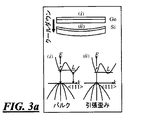
例示的な半導体基板12は、高抵抗Si上に成長されたGe膜の薄層を有することができる。これを達成するための1つの潜在的な技術は、当技術分野で知られているように、水素雰囲気において複数の成長およびアニールステップを経て、シリコン(Si)上に貫通転位密度が低い高品質のゲルマニウム(Ge)を成長させる。この技術では、Ge薄膜は、Si層上にヘテロエピタキシャル成長させられ、水素(H2)雰囲気においてより高い温度でその場アニールされる(in-situ annealed)。これによって、表面粗さが90%低減され、最初の数百オングストロームにおける応力緩和を促進する。その後のGeの成長は、仮想Ge格子上でのホモエピタキシャル成長であり、追加の欠陥が形成されず、成長膜が下地基板の結晶格子を引受ける。使用されたGe成長技術の潜在的な利点は、得られた歪みGe膜が、バルクGeと比べて、通信波長(たとえば、約1550nmの波長)で一桁高い吸収係数を提供できることである。その理由は、SiとGeとの間の熱膨張係数の不整合により生じた引張歪み(図3aに示される)によって、ゲルマニウム(Ge)吸収スペクトルの赤方偏移(図3bに示される)が発生するからである。図3bは、引張歪みに起因するGe吸収スペクトルの赤方偏移を示し、より具体的には、0.16%の推定引張歪み下で成長したGe層の実験吸収係数−光子エネルギーは、引張歪みによって吸収端が47nm赤方偏移することを示している。図3aは、Ge膜において二軸引張歪みによるバンドの変化を示している。図3a〜3bに示されたグラフの詳細について、A. K. Okyay, A. Nayfeh, T. Yonehara, A. Marshall, P. C. Mclntyre, K. C. Saraswat, "High Efficiency MSM Photodetectors on Heteroepitaxially Grown Ge on Si", Opt. Lett., 31, pp. 2565-2567, 2006を参照。重い正孔および軽い正孔の価電子帯の最大値が増大すると、ゾーン中心の伝導帯の最小値が減少する。引張歪みに起因して、直接バンドエネルギーが低減する。インジウムガリウムヒ化物(InGaAs)の場合、薄層を半絶縁性インジウムリン化物(InP)基板上のインジウムアルミニウムヒ化物(InAlAs)バッファ層上にエピタキシャル成長させることができる。上記に列挙した製造技術のいくつかは、既知であり、当業者によって理解される。
The
アンテナ組立体
アンテナ組立体14は、半導体基板12上に作製され、テラヘルツ(THz)放射を発する(光伝導波源)またはTHz放射を検出する(光伝導検出器)ために使用される。当業者は、あらゆる様々の光伝導テラヘルツアンテナの構成および配置が本明細書に記載された光伝導装置ととも使用することができ、かつ、このことは、いずれかの特定の実施形態に限定されないことを理解するであろう。たとえば、アンテナ組立体14は、モノポールアンテナ、バタフライアンテナ、ダイポールアンテナ、スパイラルアンテナ、折返しダイポールアンテナ、対数周期アンテナ、ボウタイアンテナ、または当技術分野で知られている任意の他の適切な光伝導THzアンテナ構成であってもよい。図1において、アンテナ組立体14は、ダイポールアンテナとして示されている。図4は、ダイポールアンテナの代わりに、ボウタイアンテナ組立体34を用いる光伝導装置10の別の実施形態を示している。以下でさらに詳述するように、両方の実施形態において、アンテナ組立体は、数多くのプラズモン接触電極を用いて装置の性能を向上させる。
Antenna Assembly The
光伝導装置10を光伝導テラヘルツ(THz)波源として実現するために、光伝導体組立体16は、THzアンテナと一体化されている。アンテナに供給される光生成電流の振幅は光伝導体活性領域に線形的に比例するため、小さなRC時定数と高い放射耐性とを維持しながら、光伝導性領域を増加させるように、一連の密集したダイポールアンテナを設計することができる。アンテナ放射パラメータ、光伝導体の寄生成分および光伝導体活性領域に基づいて注入された電流量を組合わせることによって、例えば、最大の放射出力を得ることを目的としてアンテナアレイ構造を最適化するために、ADSおよびHFSSソフトウェアパッケージを用いることができる。
In order to realize the
光伝導装置10の出力パワーは、共振キャビティ、高い放射耐性と広い帯域幅を有するアンテナ、およびアンテナアレイを用いることと、適切なインピーダンス整合技術を用いることによって、さらに増強することができる。たとえば、「C.W. Berry, M. Jarrahi, "Principals of Impedance Matching in Photoconductive Antennas " Journal of Infrared, Millimeter and Terahertz Waves, 33, 1182-1189, 2012」により開示された技術、特徴および実施形態のいずれも本明細書に開示された例示的な光伝導装置に用いてもよい。その文献内容の全体は、参照により本明細書に組込まれる。
The output power of the
光伝導体組立体
光伝導体組立体16は、同様に半導体基板12上に作製され、半導体基板12の光吸収領域(たとえば、層30)へのポンプ吸収をプラズモニックに増強することによって光伝導装置10の量子効率を改善するように設計されている。例示的な実施形態によれば、光伝導体組立体16は、光伝導波源10における光−テラヘルツ変換効率を増強するためにアレイ状に配置された数多くのプラズモン接触電極50を含む。本明細書で使用された「プラズモン接触電極」は、光伝導体組立体の一部でありまたは光伝導体組立体に連結されるとともに、以下でより詳細に説明するように、電極により決められたサブ波長装置の活性領域への光結合を向上させる表面プラズモン波または表面波を励起し、さもなければそれを促進する任意の電極構造を広く意味する。。一実施形態において、プラズモン電極50は、平行に配置された数多くの薄い指状電極を含む。プラズモン電極50は、電極間にサブ波長の金属開口を形成するように、半導体基板12の頂部層30上に作製される。プラズモン増強は、密集したプラズモン接触電極50を、ナノスケールの電極幅およびナノスケールの電極間隔(たとえば、約200nm未満)を有する周期的な配列に構成することによって、達成される。これにより、光生成キャリアを超高速に収集することを可能にし、従来の光伝導体に比べて高い量子効率をもたらす。プラズモン接触電極50は、アンテナ組立体14から延在するように、アンテナ組立体14と一体に形成されてもよく、別体のアレイまたは他の構造として別個に形成された後、アンテナ組立体に接続されてもよい。適切なプラズモン接触電極金属のいくつかの非限定的な例としては、金(Au)、銀(Ag)、チタン(Ti)、ニッケル(Ni)、およびそれらの各種合金が挙げられる。
Photoconductor
当業者は、サブ波長接触電極の開口またはギャップへの光吸収は、一般的に回折限界によって厳しく制限されることを理解するであろう。しかしながら、周期的に配置されたプラズモン接触電極50を有する光伝導体組立体16は、表面プラズモン波を励起可能なようにサブ波長接触電極を構成することにより、回折限界を回避する。表面プラズモン波の励起は、周期的に配置されたプラズモン接触電極50の上部で、入射光ビームの電界線(electric field lines)が曲がることを可能にし、よって入射光の励起が電極50によって妨げられない。このことは、特に特定の実施形態において装置の活性領域の重要部分がプラズモン電極50により覆われている場合に、かなり重要である。金属開口またはスリットを有するプラズモン電極を、広帯域テラヘルツ空間ビーム変調器において実施することができ、光伝導アンテナの効率/帯域幅積を増強する、プラズモニックに増強された光導電アンテナへの光の局在においても実施することもできるが、これらはまた可能性にすぎない。
One skilled in the art will understand that light absorption into the aperture or gap of a subwavelength contact electrode is generally severely limited by the diffraction limit. However, the
以下で詳しく説明するように、プラズモン接触電極50を光伝導体16に組込むことにより、サブ波長の間隔を有する接触電極を透過する光ビームの透過量を著しく低減する特定の回折限界を克服することができる。その結果、光生成キャリアの超高速輸送は、量子効率に重大な制限を課すことはない。狭いバンドギャップを有する半導体装置、たとえばGeに対して、装置設計に関する課題の1つは、高い暗電流である。高い暗電流課題は、プラズモン接触の金属、特徴的な構造の大きさおよび形状を考慮して、非対称のプラズモン接触電極を使用することによって解決することができる。
As described in detail below, by incorporating the
励起された表面プラズモン波の概略図は、図4の拡大挿入図に示されている。電極の格子形状は、TM偏光の光ポンプの入射の際に、周期的な金属格子界面に沿って表面プラズモン波を励起するように設計されている。表面プラズモン波の励起は、光ポンプの大部分がナノスケール格子を通って光吸収半導体基板12内に伝送されることを可能にし、プラズモン接触電極50に非常に近接する光ポンプの強度を増強する。その結果、アノード電極またはアンテナ組立体14の端子までの平均光生成電子輸送経路の長さは、従来の光伝導性エミッタに比べて大幅に減少される。したがって、光伝導体組立体16にとって、電極間隔を最小化してアノード電極までの平均光生成電子輸送経路の長さを最小化しながら、光吸収半導体基板12内への光ポンプ伝送を最適化することが望ましい。
A schematic of the excited surface plasmon wave is shown in the enlarged inset of FIG. The grid shape of the electrodes is designed to excite surface plasmon waves along the periodic metal grid interface upon incidence of a TM polarized optical pump. The excitation of the surface plasmon wave allows most of the optical pump to be transmitted through the nanoscale grating into the light absorbing
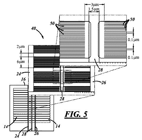
図5を参照して、図面には、アンテナ組立体14および光伝導体組立体16が示されている。プラズモン接触電極アレイは、いくつかの拡大挿入図により詳細に示されている。図示のように、プラズモン接触電極50の約半分は、第1アンテナ端子24に電気的に連結され、第1アンテナ端子に光生成キャリアを提供する。プラズモン接触電極50の他の半分は、第2アンテナ端子26に電気的に連結され、第2アンテナ端子に光生成キャリアを提供する。任意部品である細長分離部材28は、プラズモン電極を2つのグループに分離または区画する。プラズモン接触電極50の半分は正のキャリアを収集し、他の半分は負のキャリアを収集する。プラズモン接触電極の間隔および構成は、図5に示された例示と異なってもよいが、プラズモン接触電極の間隔は、相当重要である。たとえば、アンテナ端末24に接続されたプラズモン接触電極がアンテナ端子26に接続されたプラズモン接触電極に近すぎると、静電容量に関連する問題が生じるか、またはプラズモン接触電極領域の全体に沿って光キャリアをプラズモン接触電極に超高速でドリフトさせるのに必要な十分に高い電界レベルを妨げる可能性がある。また、光伝導体組立体16が互いの間に間隔を有するプラズモン接触電極のセグメントまたはクラスタに区画または配置されることが示されているが、これは必須ではない。
Referring to FIG. 5, the drawing shows an
図6は、多少異なる光伝導体組立体設計を有する光伝導波源の別の潜在的な実施形態を示している。光伝導装置110は、半導体基板112と、アンテナ組立体114と、光伝導体組立体116と、レンズ118とを含む。光伝導装置110は、光伝導体組立体が多数の十字形プラズモン接触電極130を含むことを除き、図1に示された実施形態と同様である。光伝導体組立体116は、本明細書に開示される他の光伝導体組立体と同様に、プラズモン開口として機能することができ、以下の形状を有するさまざまな幾何学的形状および構成を有するナノスケール開口の二次元アレイであり得る:格子状、矩形、十字形、C字形、H字形、スプリットリング共振器、円形穴、または長方形穴(図6に示されたものは、十字形である)。
FIG. 6 illustrates another potential embodiment of a photoconductive wave source having a slightly different photoconductor assembly design. The
光吸収半導体の内部に埋め込まれた高アスペクト比のプラズモン接触電極を使用することは、数多くのキャリアを光伝導体接触電極の近傍で発生させることを可能にし、したがってテラヘルツ放射をさらに増強させることができる。よって、プラズモン電極の高さを光ポンプ吸収深さよりも大きい寸法に延長すると、光キャリアの大多数を光伝導接触電極に超高速で輸送することを可能にし、テラヘルツ波の発生に効果的に寄与することができる。したがって、光伝導性エミッタのDC電流を抑制するためおよび連続波光伝導エミッタにおいて望ましくない弱め合う干渉を防止するために使用され得る短キャリア寿命の半導体を使用する必要性を排除することができる。高品質の結晶半導体に比べて低キャリア移動度および低熱伝導率を有する短キャリア寿命半導体を使用する必要性を排除することは、将来の高出力、高効率の光伝導テラヘルツ波エミッタに重要な影響を与えることができ、特殊な機能を有する光吸収半導体に基づく新世代の光伝導テラヘルツ波エミッタ(たとえば、優れたキャリア移動度を有するグラフェン系の光伝導性エミッタ、または優れた熱伝導率を有するGaN系光伝導性エミッタ)につながる可能性もある。 Using a high-aspect-ratio plasmon contact electrode embedded inside a light-absorbing semiconductor allows many carriers to be generated in the vicinity of the photoconductor contact electrode, thus further enhancing terahertz radiation. it can. Therefore, if the height of the plasmon electrode is extended to a size larger than the absorption depth of the optical pump, the majority of the optical carriers can be transported to the photoconductive contact electrode at an extremely high speed, effectively contributing to the generation of terahertz waves. can do. Thus, the need to use short carrier lifetime semiconductors that can be used to suppress the DC current of the photoconductive emitter and to prevent unwanted destructive interference in continuous wave photoconductive emitters can be eliminated. Eliminating the need to use short-carrier lifetime semiconductors with low carrier mobility and low thermal conductivity compared to high-quality crystalline semiconductors will have a significant impact on future high-power, high-efficiency photoconductive terahertz wave emitters New generation photoconductive terahertz wave emitters based on light-absorbing semiconductors with special functions (for example, graphene-based photoconductive emitters with excellent carrier mobility, or with excellent thermal conductivity) GaN-based photoconductive emitter).
図7aは、上述したように、数多くの二次元プラズモン接触電極50を有する光伝導体組立体を示す。図7b〜cは、数多くの三次元プラズモン電極150を有する光伝導体組立体を示す。本明細書中に記載された「二次元プラズモン接触電極」は、一般的に、非常に薄くて、幅寸法または長さ寸法に対して小さい高さ寸法を有するプラズモン電極(図7aに概略的に示された例を参照)を指す。本明細書に記載された「三次元プラズモン接触電極」は、一般的に、はるかに厚くて、幅寸法または長さ寸法に対してより大きい高さ寸法を有するプラズモン電極(図7bに概略的に示された例を参照)を指す。三次元プラズモン接触電極は、二次元の電極に比べてより大きい量で半導体基板の表面から延在するため、高アスペクト比を有すると記載される場合がある。これらのプラズモン接触電極配置は、従来の設計に比べて、テラヘルツ波の放射を1桁以上に増強した。光吸収基板における光生成キャリア密度と、電界データと、マルチフィジックス有限要素解法(COMSOL)における伝統的なドリフト拡散モデルとを組合わせて、光ポンプインパルスに応じて誘起された光電流を計算することによって、分析対象とした図示の二次元および三次元のプラズモン接触電極を有する光伝導体のインパルス応答およびインパルス応答性に関して、いくつかの見積もりが得られた。これらの見積もりは、三次元プラズモン接触電極(図7b〜7c)を有する光伝導テラヘルツ波エミッタが、二次元プラズモン接触電極を有する類似の光伝導装置(図7a)に比べて、テラヘルツ波出力を2桁以上に増強していることを示している。したがって、三次元プラズモン接触電極150を有する光伝導テラヘルツ波エミッタは、同一の動作条件下で、プラズモン接触電極を備えない従来の光伝導テラヘルツ波エミッタに比べて、4桁以上大きなテラヘルツ放射を提供することができる。
FIG. 7a shows a photoconductor assembly having a number of two-dimensional
前述の実施例は、単にいくつかの可能性を説明することを意図しているため、他の光伝導体組立体およびプラズモン接触電極の実施形態もまた、本明細書に開示された光伝導装置10とともに使用することができる。 Since the above examples are only intended to illustrate some possibilities, other photoconductor assembly and plasmon contact electrode embodiments are also disclosed in the photoconductive devices disclosed herein. 10 can be used.
他の部品、配置および特徴的な構造など
装置の性能および操作性などを向上させるために、光伝導装置10は、さまざまな他の光学部品および非光学部品を含んでもよい。たとえば、より高い量子効率およびより高いテラヘルツ波出力を達成するために、特殊設計の光学拡散器、一次元または二次元のレンズのアレイが使用され、光の入力またはポンプビームを導光する。そのため、大量のアレイ光伝導装置を採用しつつ、光の入力またはポンプビームは、光伝導体組立体16の活性領域のみに入射され、THz放射に寄与しない装置の残り領域に浪費されない。
Other Parts, Arrangements, and Characteristic Structures To improve the performance and operability of the device, the
使用することができるの別の潜在的な特徴は、誘電体パッシベーション層である。この誘電体パッシベーション層は、半導体界面でフレネル反射を低減し、したがって光吸収半導体基板への光ポンプ伝送を増強することができる。従来の光伝導体において、光吸収半導体への光ポンプ伝送は、ポンプ波と半導体界面との間の直接的な相互作用による結果であるのに対し、本明細書において説明したプラズモン電極を有する光伝導体において、光吸収半導体への光ポンプ伝送は、励起された表面プラズモン波との結合を含んでいる。プラズモン光伝導体の場合には、パッシベーション層の厚さは、光吸収半導体への光伝送を100%まで達成するように最適化することができる。図8は、適切なパッシベーション層160の非限定的な一例を示している。図において、SiO2パッシベーション層(たとえば、厚さ150nm)が、プラズモン接触電極を有する現行の光伝導体とともに使用される。パッシベーション層160を用いてプラズモン電極50を完全に封入してもよく(図示のように)、または、プラズモン接触電極50がパッシベーション層を通って延在するように、パッシベーション層を用いて半導体基板12の上面のみを覆ってもよい。パッシベーション層160は、SiO2以外の適切な材料、たとえばSiNまたはSi3N4などを多数含んでもよい。
Another potential feature that can be used is a dielectric passivation layer. This dielectric passivation layer can reduce Fresnel reflection at the semiconductor interface and thus enhance optical pump transmission to the light absorbing semiconductor substrate. In conventional photoconductors, optical pump transmission to a light-absorbing semiconductor is the result of a direct interaction between the pump wave and the semiconductor interface, whereas light having a plasmon electrode as described herein. In a conductor, optical pump transmission to a light-absorbing semiconductor includes coupling with an excited surface plasmon wave. In the case of a plasmon photoconductor, the thickness of the passivation layer can be optimized to achieve up to 100% light transmission to the light absorbing semiconductor. FIG. 8 shows a non-limiting example of a
提案された光伝導装置10とともに、低抵抗のバイアスネットワークを使用してもよい。このようなバイアスネットワークは、比較的高い暗電流を有する低バンドギャップエネルギー半導体(たとえば、Ge、InGaAs)を用いた場合に、特に有用であり得る。
A low resistance bias network may be used with the proposed
上記のように、光伝導装置10は、光伝導テラヘルツ検出器として使用することもできる。光伝導テラヘルツ波エミッタと同様に、従来の光伝導テラヘルツ検出器の主な制限は、低応答性および低感度であり、これは、典型的には、従来の光伝導体の高量子効率と超高速動作との間の固有のトレードオフの結果である。本明細書に記載されたプラズモン接触電極構造の別の潜在的な利点は、光伝導体の接触電極までの光生成キャリアの輸送経路を減少させることによって、従来の光伝導テラヘルツ検出器に比べて、著しく高くなった応答性および検出感度を提供することである。さらに、光伝導体の寄生容量を大幅に増大させることなく、装置の活性領域を大きくすることができるため、より高い光ポンプ出力レベルでより高い検出器の応答性を達成することができる。光伝導テラヘルツ検出器の試作品の性能は、時間−領域テラヘルツ分光装置構成により特徴付けられる。一部の実験結果は、プラズモン接触電極を組込むことよって、検出器の応答性を2桁以上高めることができることを示している。
As described above, the
動作
光伝導波源10の動作は、光吸収半導体基板12において電子正孔対を生成する入射光ポンプに基いている。生成されたキャリアは、光伝導体組立体16に印加された電圧によって、対応するプラズモン接触電極50に向かってドリフトされる。プラズモン接触電極50において収集された光電流は、テラヘルツアンテナ組立体14を駆動する。テラヘルツアンテナ組立体14は、光伝導体組立体16に接続されているか、さもなければ光伝導体組立体16と一体化されている。生成された光電流が光ポンプの波形と同様であるため、サブピコ秒光パルスを使用するまたはテラヘルツ周波数分の周波数が異なる2つの連続波光ビームにヘテロダイン処理を施すことによって、それぞれ、パルスまたは連続波テラヘルツ電流は、テラヘルツアンテナ組立体14に結合される。所望のテラヘルツ周波数領域において効率的に動作させるために、光生成キャリアをプラズモン接触電極50に輸送する時間は、テラヘルツ振動周期の逆数であるべきである。
Operation The operation of the
光伝導波源10は、サブピコ秒の応答時間を示し、長いキャリア寿命または短いキャリア寿命の半導体基板とともに、高品質の結晶系半導体基板12上に作製することができる。光伝導波源10の超高速応答は、入射光の大部分を光伝導体組立体16のプラズモン接触電極50の近傍に集中させる表面プラズモン波の励起に起因し、したがって光伝導体の量子効率を大きく犠牲にすることなく、光生成キャリアの超高速収集を可能にする。一実施形態において、超高速光伝導波源10は、高品質の結晶性半導体から作られた光吸収半導体基板12と、格子状のプラズモン接触電極を有する光伝導体組立体16とを含む。格子の周期またはピッチと電極の間隔または開口の大きさとは、入射光ビームの波長よりも著しく小さい。したがって、金属格子表面で表面プラズモン波を励起することができる。励起された表面プラズモン波は、入射光をサブ波長の格子開口を通って光吸収半導体基板12内に効率的に伝送することを支援する。さらに、伝送された光波の強度は、プラズモン接触電極50の近傍で増強されるため、光生成キャリアをプラズモン接触電極に輸送する平均時間を短縮し、高量子効率および超高速動作を同時に可能にする。
The
正孔に比べて電子が著しく高い移動度を有するため、および接触電極付近のバイアス電界が非線形的に増加するため、光ポンプまたは光源をアンテナ組立体14のアノードコンタクトに非対称的に接近している光伝導体組立体16の光伝導ギャップ上に集光させ、テラヘルツ放射を最大化することができる。言い換えると、本明細書に記載の光伝導装置10は、光源がアンテナ組立体14の接触電極の一方をポンプするように非対称的にポンプされてもよく、光源がアンテナの接触電極の両方をポンプするように対称的にポンプされてもよい。
The electron pump or light source is asymmetrically approaching the anode contact of the
要約すると、光伝導波源10は、ナノスケールのプラズモン接触電極50を有する光伝導体組立体16を含む。プラズモン接触電極50は、光生成キャリア輸送経路を著しく低減し、従来の光伝導テラヘルツ波源の効率を制限し得る短キャリア寿命の基板を必要とせずに超高速動作を可能にする。高量子効率を維持しながら超高速動作を達成する能力は、将来の高出力テラヘルツ波エミッタにとって有用である。以下では、光伝導装置10に関する他の潜在的な局面およびその動作を論ずる。
In summary, the
製造
以下の説明は、製造または作製工程に関し、3次元プラズモン接触電極およびガリウムヒ化物(GaAs)半導体基板が使用される特定の非限定的な実施形態に向けられている。既に何度も述べたように、光伝導装置は、これに限定されず、本明細書に記載されたあらゆるさまざまな特徴および実施形態を含むことができる。この例示的な作製工程は、SiO2膜の堆積から始まり、その後、ナノスケールのGaAs格子をエッチングするための硬質マスクを形成するために、ナノスケール金属格子(たとえば、Ni)をパターン化する。その後、SiO2膜およびその下にあるGaAs基板は、金属硬質マスクに従ってエッチングされる。Ti/Auをスパッタリングし、続いてリフトオフすることによって、プラズモン接触電極を形成することができる。最後に、GaAs格子の上面を覆うように、誘電体(たとえば、SiO2)パッシベーション層を堆積させることができる。
Manufacturing The following description is directed to specific non-limiting embodiments in which a three-dimensional plasmon contact electrode and a gallium arsenide (GaAs) semiconductor substrate are used with respect to the manufacturing or fabrication process. As already mentioned many times, the photoconductive device is not so limited and can include any of a variety of features and embodiments described herein. This exemplary fabrication process begins with the deposition of a SiO 2 film and then patterns a nanoscale metal lattice (eg, Ni) to form a hard mask for etching the nanoscale GaAs lattice. Thereafter, the SiO 2 film and the underlying GaAs substrate are etched according to the metal hard mask. Plasmon contact electrodes can be formed by sputtering Ti / Au followed by lift-off. Finally, a dielectric (eg, SiO 2 ) passivation layer can be deposited over the top surface of the GaAs lattice.
集束イオンビームを用いて、高アスペクト比を有する厚いフォトレジスト層をパターン化してもよい。数多くの光伝導体アレイ用に、より良い均一性およびより速いパターン化速度を達成するために、ナノインプリンティング、セルフアセンブリ技術および集束イオンビームを用いてもよい。 A thick ion layer having a high aspect ratio may be patterned using a focused ion beam. Nanoimprinting, self-assembly techniques and focused ion beams may be used to achieve better uniformity and faster patterning speed for many photoconductor arrays.
代わりに、あらゆる他の製造または作製工程を使用できることは、当業者にとって理解できるであろう。 It will be appreciated by those skilled in the art that any other manufacturing or fabrication process can be used instead.
テスト、シミュレーション、発見および装置構成など
以下の段落および段落に参照される図面は、光伝導波源10の例示的な実施形態の異なるテスト、シミュレーション、発見および装置構成などを記載し、装置のさまざまな動作態様を説明することを意図している。これらのテストおよびシミュレーションに利用される具体的な実施形態は、限定することを意図せず、本発明の光伝導装置の異なる特徴または態様をさらに説明または例示するために提供される。
Tests, Simulations, Discovery and Device Configurations, etc. The drawings referenced in the following paragraphs and paragraphs describe the different tests, simulations, discovery and device configurations, etc. of the exemplary embodiment of the
超高速光伝導体において誘起された光電流および光伝導テラヘルツ波エミッタから放射されたテラヘルツ波出力を増強するというプラズモン接触電極50のインパクトは大きい。同様に、パルス波動作時および連続波動作時に、櫛形接触電極を有するまたは有しないさまざまなテラヘルツアンテナおよび大面積の光伝導装置を備える光伝導テラヘルツ波エミッタからの放射パワー、および、櫛形接触電極を有するまたは有しないさまざまなテラヘルツアンテナおよび大面積の光伝導装置を備える光伝導テラヘルツ検出器の検出感度を増強するために、この増強構想を適用することができる。言い換えると、本明細書に開示されたさまざまなプラズモン接触電極は、異なる半導体基板、アンテナ組立体、光伝導体組立体、レンズおよびバイアスネットワークを含む多種多様の他の部品とともに、使用することができる。
The impact of the
提案された光伝導装置10の1つの潜在的な利点は、任意の大きさの装置領域への光伝送をプラズモニックに増強することができるという拡張可能性である。その理由は、装置の容量性寄生が放射アンテナの長さに沿って分布しているため、周波数の関数としてのアンテナ効率およびアンテナインピーダンス整合はいずれも低下しない。密集した接触電極を有する超高速分布型光伝導体の量子効率を増強するために、類似のプラズモン電極構成を使用することができる。
One potential advantage of the proposed
提案された光伝導装置10のさらに別の潜在的な利点は、プラズモン接触電極領域付近の光生成キャリア濃度を増強し、その結果、量子効率を改善することである。
Yet another potential advantage of the proposed
提案された光伝導装置10のの別の局面は、キャリア遮蔽効果を抑制する能力を含んでいる。遮蔽効果は、高ポンプ強度のときに生じ始める。この時、小さい領域に蓄積された数多くの光生成キャリアは、キャリアドリフト電界を遮蔽する。キャリア遮蔽効果を抑制するために、遮蔽電界がキャリアドリフト速度を低下させることによって光伝導体テラヘルツ電流を減少させ始める強度を最大ポンプ強度として決定する。光伝導体の全体寸法を、所定のポンプ出力においてポンプ強度がこの最大ポンプ強度を超えないように選択することができる。ポンプ結合効率、ポンプ/テラヘルツ波伝搬損失、およびポンプ/テラヘルツ波速度整合要件は、従来の光伝導装置の最大テラヘルツ波出力パワーを制限する重要な障害となっている。当業者に理解されるように、光伝導体へのポンプの結合および光伝導体からのテラヘルツの分離が自由空間中で並行して行われているため、光伝導波源10は、進行波分布型光伝導体に関連する同じ制限に直面しない。
Another aspect of the proposed
キャリア遮蔽効果および熱影響を抑制するために、光伝導波源10は、高出力光ポンプを、プラズモン接触電極または素子の二次元アレイからなる比較的大きな光伝導活性領域上に広げる。従来の設計では、大きな光伝導活性領域からの容量負荷は、RCロールオフのため、放射アンテナに連結される光生成テラヘルツ電流を大きく制限する。この制限を解決するために、光伝導波源10は、アンテナ組立体14に沿った分布型容量性負荷として光伝導体組立体16を一体化している。
In order to suppress carrier shielding effects and thermal effects, the
他のテラヘルツ波源と比較した、光伝導装置10のさらに他の潜在的な利点は、装置の周波数が広範囲で連続的に可変であることである。ほとんどの他の光伝導テラヘルツ波源と同様に、プラズモン接触電極50を有する光伝導波源10の周波数可変範囲は、使用されるテラヘルツアンテナの放射帯域幅によって決定される。
Yet another potential advantage of the
光伝導装置10の別の潜在的な局面によれば、二次元プラズモンアレイ上に光ポンプを広く分布させることは、指向性が高い出力を有するテラヘルツ波ビームを達成することに役立ち得る。提案された光伝導装置10の高指向性放射パターンは、特にテラヘルツをコリメート/集束する部品の使用が制限され得るテラヘルツ波リモート検知および遠隔化学検出応用に対して望ましい。また、光伝導装置10から出力されるテラヘルツ放射を、光伝導体素子に印加されたバイアス電圧Vbias (i)の特定の分布によって、制御可能に偏向させることができる。
According to another potential aspect of the
提案された光伝導装置10の別の望ましい局面は、1065nmおよび1550nm波長でまたはその付近での高効率動作である。波長1550nmおよび1065nm付近の通常の光ファイバ遠距離通信帯域において、外部共振器型ダイオードレーザ(ECDL)などの純スペクトルダイオードレーザ光源の出力を数十ワットまで高めることができる小型のエルビウム添加光ファイバ増幅器およびイッテルビウム添加光ファイバ増幅器が開発されている。ファイバレーザの高い可変性(たとえば、数十nm程度)は、連続広帯域(たとえば、数THz)のスペクトル測定を可能にし、ファイバレーザの狭いスペクトル線幅(たとえば、1MHz未満)は、密集した吸収線(たとえば、数十MHz程度の間隔)を有する化学物質の正確な同定を可能にする。さらに、光ファイバは、体積を非常に小さくするとともに振動に対する感度を最小にしながら、周波数がオフセットされた2つのレーザを組合わせるために理想的である。提案された光伝導体を特徴付けるために、IPGフォトニクス社により市販されている2つのエルビウムファイバレーザ(ELTシリーズ)を光源として使用してもよい。このレーザは、1540〜1605nmの波長可変範囲、300KHz未満のスペクトル線幅、30分間にわたって0.1nm未満の波長安定性および0.1dBの出力安定性を有する最大25Wの出力パワーを提供する。これは、あくまで例に過ぎず、代わりに他の光源を使用してもよい。
Another desirable aspect of the proposed
再び図8を参照する。図8は、有限要素解法COMSOLによって計算された、TM偏光の光ビーム(λ=1550nm)が、薄いIn0.53Ga0.47As基板上に設けられた金の接触格子(ピッチ=120nm、金属幅=60nm)を有する光伝導体と相互作用する様子を示している。(光出力の流れ方向を表す)矢印は、伝播光線が金属格子の上面でどのように曲がって、光吸収基板と高効率に結合されるかを示している。図8に示すように、光ビームは、金属格子の角部付近に局所的に集中しており、その結果、光伝導体接触電極のすぐ近傍において非常に高濃度の光生成電子−正孔対が生成される。図9aに示されるように、格子の光透過スペクトルは、In0.53Ga0.47Asが吸収するとともにInP基板が透明である波長において、広帯域である。1550nm波長において、5%を超える入射光の出力は、厚さ60nmのIn0.53Ga0.47As層に吸収される。残りの光出力は、追加の加熱をもたらすことなく、透明基板を通過する。図9aは、金の格子(ピッチ=120nm、金属幅=60nm、高さ=20nm)を通過して、InP基板上に設けられた厚さ60nmのIn0.53Ga0.47As層への光伝送および外部量子効率を示している。 Refer to FIG. 8 again. FIG. 8 shows a gold contact grating (pitch = 120 nm, pitch = 120 nm) with a TM polarized light beam (λ = 1550 nm) calculated on a thin In 0.53 Ga 0.47 As substrate, calculated by the finite element solution COMSOL. It shows the interaction with a photoconductor having a metal width = 60 nm. The arrows (representing the flow direction of the light output) indicate how the propagating light beam bends on the top surface of the metal grating and is coupled with the light absorbing substrate with high efficiency. As shown in FIG. 8, the light beam is locally concentrated near the corners of the metal lattice, resulting in a very high concentration of photogenerated electron-hole pairs in the immediate vicinity of the photoconductor contact electrode. Is generated. As shown in FIG. 9a, the light transmission spectrum of the grating is broadband at wavelengths where In 0.53 Ga 0.47 As absorbs and the InP substrate is transparent. At the 1550 nm wavelength, the incident light output exceeding 5% is absorbed by the In 0.53 Ga 0.47 As layer having a thickness of 60 nm. The remaining light output passes through the transparent substrate without causing additional heating. FIG. 9a shows the result of passing through a gold lattice (pitch = 120 nm, metal width = 60 nm, height = 20 nm) to an In 0.53 Ga 0.47 As layer with a thickness of 60 nm provided on an InP substrate. Optical transmission and external quantum efficiency are shown.
図9bを参照して、光キャリアが0.4Vのバイアス電圧下においてバイアス電界線に沿って移動すると仮定すると、分析される光伝導体の光電流インパルス応答は、基板内の光強度分布を用いて算出することができる。比較用の基準値として、従来の光伝導体の光電流インパルス応答は、300fsのキャリア寿命を有する無限に厚い光吸収In0.53Ga0.47As基板上に作製された、2μmの接触格子ピッチおよび0.05のデューティサイクルを有するものを用いて計算される。光電流インパルス応答は、光伝導体の活性領域によって正規化され、図9bに示されている。従来の光伝導体に比べて、プラズモン接触電極50を有する光伝導体源10は、一桁高い光電流インパルス応答を提供できる。したがって、多数のプラズモン接触電極50を有する光伝導体組立体16をアンテナ組立体14と一体化することは、既存の光伝導テラヘルツ波源よりも著しく高いテラヘルツ波出力を提供することができる。さらに、In0.53Ga0.47Asのような特定の半導体基板材料を利用すると、光伝導波源10を広く利用可能な遠距離通信ファイバレーザおよび部品に適合させることができる。したがって、光伝導波源10は、光伝導テラヘルツ波の実用的生成に非常に有望であり、超高速動作および高量子効率動作を同時に可能にする。
Referring to FIG. 9b, assuming that the photocarrier moves along the bias field line under a bias voltage of 0.4V, the photocurrent impulse response of the analyzed photoconductor uses the light intensity distribution in the substrate. Can be calculated. As a reference value for comparison, the photocurrent impulse response of a conventional photoconductor is a 2 μm contact grating fabricated on an infinitely thick light absorbing In 0.53 Ga 0.47 As substrate with a carrier lifetime of 300 fs. Calculated using a pitch and a duty cycle of 0.05. The photocurrent impulse response is normalized by the active region of the photoconductor and is shown in FIG. 9b. Compared to conventional photoconductors, the
図10a〜10bは、InGaAsではなくゲルマニウム(Ge)からなる頂部薄層30を含む半導体基板への光ポンプ透過率をプラズモニックに増強する類似例を示す。より具体的には、図10aは、様々な光学波長においてプラズモン接触電極50の幾何学的形状がゲルマニウム(Ge)層へのTM偏光された光学励起の伝送にどのように影響するかを示している。厚さ20nmの金属に対し、プラズモン接触電極の電極幅および間隔を100nm未満にすれば、1550nmの波長において50%超の透過率が期待できる。最大の透過率は、半導体−空気界面での反射により制限される。一方、図10bは、1550nmのポンプ波長において60nmの電極幅および間隔を有するプラズモン接触電極50の周期的配列に沿った光出力密度分布の断面図を示している。図10bは、ゲルマニウム(Ge)層30への高透過率を達成するために、TM偏光の光学場線(optical field lines)が金属電極の上でどのように曲げられるかを示している。非常に厚い金属電極を用いることによって、最大100%の透過率を提供するプラズモン電極を構成することが可能である。
FIGS. 10 a-10 b show a similar example that plasmonically enhances the optical pump transmittance to a semiconductor substrate that includes a top
次に図11を参照する。図11は、接合部の加熱による光伝導体量子効率の低下を防止するために、光伝導体活性領域を光ポンプ出力の関数としてどのように変化させるかを示すグラフである。高ポンプ出力レベルにおける装置出力パワーの低下を防止するために、たとえばゲルマニウム(Ge)から作られた頂部薄層30の接合部温度が最大接合部温度(たとえば、TJmax=200℃)を超えないように半導体基板12を設計することができる。接合部温度が最大接合部温度を超えると、急速な低下および装置故障が発生し得る。よって、最大光ポンプ出力を装置の露出面積の関数として定義することが可能である。光伝導体加熱に関する以前のいくつかの研究によると、ジュール加熱PQ、および接合部温度Tjは、以下の式で概算することができる。
Reference is now made to FIG. FIG. 11 is a graph showing how the photoconductor active region is changed as a function of optical pump output to prevent a decrease in photoconductor quantum efficiency due to heating of the junction. In order to prevent a reduction in device output power at high pump output levels, the junction temperature of the top
式中、T0:周囲環境の温度、k:バルク熱伝導率、A:光伝導体活性領域、Popt1、Popt2:周波数がオフセットされた2つのレーザからの入射光出力、R:光伝導体応答性(例示的な実施形態の1つにおいて、0.65であると測定された)、VB:接触電極またはプラズモン接触電極50間のバイアス電圧(光伝導体量子効率が最大のときに、VBは、EBwと概ね等しい)、EB:Geの破壊電界、w:光伝導体における接触電極またはプラズモン接触電極50の間隔。
Where T 0 : ambient temperature, k: bulk thermal conductivity, A: photoconductor active region, P opt1 , P opt2 : incident light output from two lasers offset in frequency, R: photoconductivity Body responsiveness (measured as 0.65 in one exemplary embodiment), V B : bias voltage between contact electrode or plasmon contact electrode 50 (when photoconductor quantum efficiency is maximum) , V B is approximately equal to E B w), E B : breakdown electric field of Ge, w: distance between contact electrodes or
図11は、接合部の加熱による光伝導体の量子効率の低下を防止するために、光伝導体の活性領域を光ポンプ出力の関数としてどのように変化させるかを示す図である。この例では、接合部温度が200℃未満に維持されている。(プロット60により示される)高欠陥InGaAs系光伝導体に比べて、(プロット62により示される)Ge系光伝導体の方が、同様に分布された活性領域に対し、装置の量子効率を低下させることなく、一桁高い光ポンプ出力を可能にする。その理由は、特定の高欠陥半導体化合物において、熱伝導率が著しく低くなるからである。 FIG. 11 is a diagram showing how the active region of the photoconductor is changed as a function of the optical pump output in order to prevent a decrease in quantum efficiency of the photoconductor due to heating of the junction. In this example, the junction temperature is maintained below 200 ° C. Compared to high defect InGaAs photoconductors (shown by plot 60), Ge photoconductors (shown by plot 62) reduce the quantum efficiency of the device for similarly distributed active regions. This enables an optical pump output that is an order of magnitude higher. The reason is that the thermal conductivity is remarkably lowered in a specific high defect semiconductor compound.
図12a〜12bは、光生成テラヘルツ電流をテラヘルツ放射ダイポールアンテナ組立体に結合させるプロセスおよび期待されるテラヘルツ波出力パワーをまとめたものである。短時間キャリア寿命の半導体に基づく従来の光伝導テラヘルツ波源の量子効率の制限に対処するために、光伝導波源10は、ナノスケール光伝導体接触電極格子を用いて、超高速動作および高量子効率動作を同時に達成する。この光伝導テラヘルツ波源は、短いキャリア寿命半導体基板の使用を回避し、高品質の結晶基板の使用を可能にする。図12aは、短キャリア寿命の光吸収半導体に基づく従来の光伝導テラヘルツ波エミッタの動作を示す模式図である。図12bは、高品質の結晶基板上に設けられたナノスケール接触電極格子に基づく光伝導波源10の一実施形態を示す。
FIGS. 12a-12b summarize the process of coupling photogenerated terahertz current to a terahertz radiating dipole antenna assembly and the expected terahertz output power. To address the quantum efficiency limitations of conventional photoconductive terahertz wave sources based on semiconductors with short carrier lifetimes,
図12bは、ナノスケール接触電極格子に基づく光伝導波源10の例示的な実施形態の概略図およびその動作を示している。光伝導体接触電極は、ダイポールテラヘルツアンテナの入力ポートに接続された2列のナノスケール金属格子からなる。格子の周期(200nm)および金属の間隔(100nm)は、入射ポンプの波長よりも小さくなるように選択される。したがって、格子の幾何学的形状は、周期的な金属格子界面に沿って表面波を励起することによって、光を金属格子を通って光吸収活性領域に効率的に伝送し得るように設計することができる。約2μmの接触電極間隔を有する従来の光伝導テラヘルツ波源に比べて、接触電極格子のナノスケール間隔は、光伝導体接触電極までの光生成キャリア輸送経路を著しく減少させる。また、2つのナノスケール金属格子配列を2μmに分離すると、テラヘルツアンテナに対する容量性負荷が低く保たれる。さらに、周期的な金属格子界面に沿って表面波を励起すると、伝送された光ポンプの強度が接触電極の角部付近において著しく増強され、光生成キャリアを接触電極に輸送する平均時間をさらに短縮する。したがって、欠陥が誘起された短キャリア寿命の半導体を使用することなく、高量子効率を維持しつつ、超高速の光伝導体動作を実現することができる。
FIG. 12b shows a schematic diagram of an exemplary embodiment of a
図12cは、TM偏光の1550nm光ポンプの光吸収を増強させるために設計されたナノスケール格子を示している。この光の波長は、市販されている高出力、波長可変および小型の光源を使用することができる光ファイバ通信波長との適合性によって選択された。1550nmのポンプ波長において高い光吸収を達成するために、光吸収半導体として、In0.53Ga0.47Asが選択される。200nmの周期、100nmの金属間隔および50nmの金属厚さを有する金の格子を使用すると、In0.53Ga0.47As光吸収領域への入射光ポンプの伝送効率を65%超にすることができる。テラヘルツ波の生成に寄与しない半導体深部領域において光キャリアが生成するのを妨げることによって、装置の応答時間をサブピコ秒に維持しかつDC光電流を低く維持するように、InP基板上に設けられたIn0.53Ga0.47As光吸収層(60nm)の厚さは選択される。設計された光伝導体の断面における光生成キャリアの濃度および光電力の流れが図12cに示される。励起された表面波は、金属−誘電体の界面に存在するため、金の電極の角部付近の領域は、最も多くのキャリア生成を示す。キャリアが電極に近接することによって、キャリア輸送の平均時間が短縮される。 FIG. 12c shows a nanoscale grating designed to enhance the light absorption of a TM polarized 1550 nm optical pump. This wavelength of light was selected for compatibility with commercially available high power, wavelength tunable and fiber optic communication wavelengths that can use small light sources. In 0.53 Ga 0.47 As is selected as the light absorbing semiconductor to achieve high light absorption at a pump wavelength of 1550 nm. Using a gold grating with a period of 200 nm, a metal spacing of 100 nm and a metal thickness of 50 nm will increase the transmission efficiency of the incident optical pump to the In 0.53 Ga 0.47 As light absorption region above 65%. Can do. Provided on the InP substrate to keep the device response time in sub-picoseconds and keep the DC photocurrent low by preventing the generation of optical carriers in deep semiconductor regions that do not contribute to the generation of terahertz waves The thickness of the In 0.53 Ga 0.47 As light absorption layer (60 nm) is selected. The concentration of photogenerated carriers and the flow of photopower in the cross section of the designed photoconductor is shown in FIG. 12c. Since the excited surface wave exists at the metal-dielectric interface, the region near the corner of the gold electrode shows the most carrier generation. Due to the proximity of the carrier to the electrode, the average carrier transport time is reduced.
図12dでは、光生成キャリアのプロファイルをバイアス電界の影響下におけるキャリア輸送ダイナミクスに組み合わせることによって、設計された光伝導体において光学インパルスによって生成されたインパルス応答電流が計算されるとともに、0.3psのキャリア寿命を有する無限に厚いIn0.53Ga0.47As基板上に作製され、2μmの接触格子ピッチおよび100nmの金属幅を有する従来の光伝導体のインパルス応答電流と比較されている。その結果は、同一の光伝導体活性領域および同一の光ポンプ強度において、ナノスケール接触電極格子に基づく光伝導体(プロット70で示す)が従来の光伝導体(プロット72で示す)に比べて、一桁高いインパルス応答電流を与えることができることを示している(図12d)。プロット70は、設計された(厚さ60nmのIn0.53Ga0.47As活性層上に作製され、200nmの格子ピッチと100nmの幅と50nmの厚さとを有するAu格子を備える)光伝導体のインパルス応答電流の計算値を示しており、プロット72は、従来の(0.3psのキャリア寿命を有する無限に厚いIn0.53Ga0.47As基板上に作製され、2μmの接触格子ピッチと100nmの金属幅とを備える)光伝導体のインパルス応答電流の計算値を示している。
In FIG. 12d, by combining the photogenerated carrier profile with the carrier transport dynamics under the influence of the bias electric field, the impulse response current generated by the optical impulse in the designed photoconductor is calculated and 0.3 ps Compared to the impulse response current of a conventional photoconductor fabricated on an infinitely thick In 0.53 Ga 0.47 As substrate with carrier lifetime and having a contact grid pitch of 2 μm and a metal width of 100 nm. The results show that for the same photoconductor active region and the same optical pump intensity, a photoconductor based on a nanoscale contact electrode lattice (shown by plot 70) is compared to a conventional photoconductor (shown by plot 72). This shows that an impulse response current that is one digit higher can be provided (FIG. 12d).
例示的な光伝導テラヘルツ波源の周波数可変範囲は、採用されたダイポールアンテナの放射帯域幅によって決定される。異なるダイポールアンテナ長さまたはより広い放射周波数を有する他のアンテナ構成(たとえば、ボウタイアンテナ、スパイラルアンテナおよび対数周期アンテナ)を有するプラズモン光伝導体アレイ素子を用いて、提案された光伝導体の動作帯域幅を拡張することが可能である。 The frequency variable range of an exemplary photoconductive terahertz source is determined by the radiation bandwidth of the employed dipole antenna. Proposed photoconductor operating band using plasmon photoconductor array elements with different dipole antenna lengths or other antenna configurations with wider emission frequencies (eg, bowtie antennas, spiral antennas and log periodic antennas) It is possible to expand the width.
図13は、ダイポールアンテナアレイに基づく例示的な光伝導波源10の平均テラヘルツ波出力パワーを放射周波数の関数として示し、広いテラヘルツ周波数において最大出力パワーになるように最適化された検証用の光伝導波源のテラヘルツ波出力パワーとの比較を示している。1.55μm波長において25Wのポンプ出力を有する周波数がオフセットされた2つの光ポンプを用いる場合、1THzにおいて15.5mWの最大テラヘルツ波出力パワーおよび(0.8THz〜1.5THz)周波数範囲にわたって1mW超の出力パワーが期待される。期待される出力パワー(プロット80)は、約1THz周波数領域において、以前に検証された光伝導波源よりも4桁以上高くなる。また、図13は、提案された光伝導体のテラヘルツ波出力パワーが、光ポンプ出力の関数として二次的に増加することを示している。非常に高い光ポンプ出力において、光伝導体活性領域は、熱影響とキャリア遮蔽効果とを抑制することを確実にし、テラヘルツ波出力パワーを光ポンプの関数として二次的に変化させることを可能にするようにスケーリングすることができる。図13において、最大の放射は、最大アンテナ放射抵抗を提供する共振周波数において発生する。潜在的な光源は、市販されている光ポンプ用の小型で携帯可能な光源を含む。
FIG. 13 shows the average terahertz wave output power of an exemplary
図14は、光伝導波源10を特徴付けるための例示的な装置構成を示す。周波数がオフセットされた2つのレーザ90は、3dBのファイバカプラによってファイバ92内で混合される。ファイバに結合されたコリメータ94は、光ビームを光伝導波源10に集束させるために使用される。10Wを超えるポンプ出力に対して、ファイバの融解を防止するため、自由空間結合を用いてもよい。出力されたテラヘルツビームは、5mmの半径および1.76mmのセットバックを有する超半球シリコンレンズ18を介して自由空間に結合され、焦電検出器により検出される。焦電光検出器の低周波ノイズを除去するために、チョッパとロックインアンプを使用することができる。図15は、本明細書に記載されたプラズモン分布型光伝導体に基づく小型、高コスト効率、高出力、波長可変の次世代光伝導波源100の1つの可能な実施形態を示している。
FIG. 14 shows an exemplary apparatus configuration for characterizing the
図16a〜16dは、従来の光伝導テラヘルツ波源をナノ間隔で離れた複数のプラズモン接触電極を有する光伝導波源10と比較する図である。図16aは、40Vのバイアス電圧およびさまざまな光学ポンプ出力において、プラズモン光伝導体エミッタおよび従来のテラヘルツ波エミッタから測定されたテラヘルツ放射を示す図である。挿入図の曲線は、対応する光電流を示している。エラーバーは、焦電テラヘルツ検出器のノイズに関連する。図16bは、プラズモンテラヘルツ波エミッタおよび従来のテラヘルツ波エミッタから測定されたテラヘルツ放射を収集された光電流に対して作成された図である。プロットで示されたデータは、さまざまな光ポンプ出力(5〜25mW)の下でさまざまなバイアス電圧(10〜40V)を含む。図16cは、相対的なテラヘルツ波出力の増強を示している。この相対的なテラヘルツ波出力の増強は、従来のテラヘルツ波エミッタによって放射されたテラヘルツ波出力に対する、プラズモンテラヘルツ波エミッタによって放射されたテラヘルツ波出力の比として定義される。最大の増強は、キャリア遮蔽効果が開始する前の低い光出力において得られる。図16dは、100mWの光ポンプにおいて、プラズモンテラヘルツ波エミッタおよび従来のテラヘルツ波エミッタから測定された最大テラヘルツ波出力を示している。各装置のバイアス電圧は、装置の破壊点まで増加される。
16a to 16d are diagrams comparing a conventional photoconductive terahertz wave source with a
理解すべきことは、前述の記載は、本発明を明確に定義するではなく、本発明の1つ以上の好ましい例示的な実施形態を説明するためであることである。本発明は、本明細書に開示された特定の実施形態に限定されるではなく、むしろ以下の特許請求の範囲によって定義される。また、上記の説明に含まれる陳述は、特定の実施形態に関連し、上記で明確に定義される場合を除き、本発明の範囲または特許請求の範囲に使用される用語の定義を限定するものとして解釈されるべきではない。他の実施形態および開示された実施形態に対するさまざまなさまざまな変更および修正は、当業者には明らかになるであろう。このような実施形態、変更および修正のすべては、添付の特許請求の範囲内に含まれることが意図されている。 It is to be understood that the foregoing description is not intended to clearly define the invention, but to illustrate one or more preferred exemplary embodiments of the invention. The invention is not limited to the specific embodiments disclosed herein, but rather is defined by the following claims. Also, the statements contained in the above description relate to the specific embodiment and limit the definition of terms used in the scope of the invention or in the claims, except where explicitly defined above. Should not be interpreted as. Various other changes and modifications to other embodiments and disclosed embodiments will be apparent to those skilled in the art. All such embodiments, changes and modifications are intended to be included within the scope of the appended claims.
本明細書および特許請求の範囲において使用されたように、「たとえば」、「例として」、「...のような」および「など」の用語、「備える」、「有する」および「含む」などの動詞および他の動詞形は、1つ以上の構成要素または他の項目の列挙と併せて使用される場合、それぞれがオープンエンドとして解釈されるべく、他の追加成分または項目を排除するものとしてみなされるべきではないことを意味する。その他の用語は、異なる解釈を必要とする文脈で使用されていない限り、それぞれ最も広い妥当な意味を用いて解釈されるべきである。 As used herein and in the claims, the terms “for example”, “as an example”, “like ...” and “etc.”, “comprising”, “having” and “including” And other verb forms such as, when used in conjunction with an enumeration of one or more components or other items, each excludes other additional components or items to be interpreted as open-ended Means that it should not be considered as. Other terms should be interpreted with the broadest reasonable meaning unless they are used in a context that requires a different interpretation.
Claims (25)
半導体基板と、
前記半導体基板上に作製されたアンテナ組立体と、
前記半導体基板上に作製され、前記アンテナ組立体に結合された光伝導体組立体とを備え、前記光伝導体組立体は、1つ以上のプラズモン接触電極を含み、
前記光伝導装置は、少なくとも1つの光源からの光入力を受光し、前記光伝導装置の量子効率を改善するために前記プラズモン接触電極を用いる、光伝導装置。 A photoconductive device for emitting or detecting terahertz (THz) radiation, comprising:
A semiconductor substrate;
An antenna assembly fabricated on the semiconductor substrate;
A photoconductor assembly fabricated on the semiconductor substrate and coupled to the antenna assembly, the photoconductor assembly including one or more plasmon contact electrodes;
The photoconductive device receives light input from at least one light source and uses the plasmon contact electrode to improve the quantum efficiency of the photoconductive device.
前記光伝導体組立体は、前記第1の薄層上に作製される、請求項1に記載の光伝導装置。 The semiconductor substrate includes a first thin layer formed on a second thick layer,
The photoconductive device of claim 1, wherein the photoconductor assembly is fabricated on the first thin layer.
前記誘電性パッシベーション層は、前記1つ以上のプラズモン接触電極の少なくとも一部を封入し、前記半導体基板への光ポンプの伝送を増強する、請求項1に記載の光伝導装置。 The photoconductive device further comprises a dielectric passivation layer formed on the semiconductor substrate,
The photoconductive device of claim 1, wherein the dielectric passivation layer encapsulates at least a portion of the one or more plasmon contact electrodes to enhance transmission of an optical pump to the semiconductor substrate.
(a)前記半導体基板において光源からの光入力を受光するステップと、
(b)前記プラズモン接触電極を用いて表面プラズモン波または表面波の励起を促進するステップとを備え、前記表面プラズモン波または表面波は、より多くの光入力が前記半導体基板に吸収されて前記半導体基板において光電流をもたらすように、前記光源からの前記光入力に影響を与え、さらに、
(c)前記半導体基板における前記光電流の第1の部分が第1のアンテナ端子に向かってドリフトし、前記半導体基板における前記光電流の第2の部分が第2のアンテナ端子に向かってドリフトするように、前記アンテナ組立体に電圧を印加するステップと、
(d)前記光電流の前記第1および第2の部分が供給されている前記第1および第2のアンテナ端子に応答して前記光伝導装置からテラヘルツ(THz)放射を発するステップとを備える、方法。 A method of operating a photoconductive device having a semiconductor substrate, an antenna assembly, and one or more plasmon contact electrodes, comprising:
(A) receiving light input from a light source in the semiconductor substrate;
(B) promoting excitation of a surface plasmon wave or surface wave using the plasmon contact electrode, wherein the surface plasmon wave or surface wave is absorbed by the semiconductor substrate so that more light input is absorbed into the semiconductor substrate. Affecting the light input from the light source to provide a photocurrent at the substrate, and
(C) The first portion of the photocurrent in the semiconductor substrate drifts toward the first antenna terminal, and the second portion of the photocurrent in the semiconductor substrate drifts toward the second antenna terminal. Applying a voltage to the antenna assembly;
(D) emitting terahertz (THz) radiation from the photoconductive device in response to the first and second antenna terminals being supplied with the first and second portions of the photocurrent; Method.
(a)前記半導体基板において光源からの光入力を受光するステップと、
(b)前記プラズモン接触電極を用いて表面プラズモン波または表面波の励起を促進するステップとを備え、前記表面プラズモン波または表面波は、より多くの光入力が前記半導体基板に吸収されて前記半導体基板において光電流をもたらすように、前記光源からの前記光入力に影響を与え、さらに、
(c)前記アンテナ組立体を介して入射するテラヘルツ放射を受け取るステップを備え、前記入射するテラヘルツ放射は前記プラズモン接触電極の間にテラヘルツ電界を誘起し、さらに、
(d)入射するテラヘルツ放射の大きさに比例する出力光電流を発生する前記誘起されたテラヘルツ電場の結果として、前記プラズモン接触電極に向かって光電流をドリフトさせるステップを備える、方法。 A method of operating a photoconductive device having a semiconductor substrate, an antenna assembly, and one or more plasmon contact electrodes, comprising:
(A) receiving light input from a light source in the semiconductor substrate;
(B) promoting excitation of a surface plasmon wave or surface wave using the plasmon contact electrode, wherein the surface plasmon wave or surface wave is absorbed by the semiconductor substrate so that more light input is absorbed into the semiconductor substrate. Affecting the light input from the light source to provide a photocurrent at the substrate, and
(C) receiving terahertz radiation incident through the antenna assembly, the incident terahertz radiation inducing a terahertz electric field between the plasmon contact electrodes;
(D) drifting the photocurrent toward the plasmon contact electrode as a result of the induced terahertz electric field generating an output photocurrent proportional to the magnitude of the incident terahertz radiation.
Applications Claiming Priority (3)
| Application Number | Priority Date | Filing Date | Title |
|---|---|---|---|
| US201261589486P | 2012-01-23 | 2012-01-23 | |
| US61/589,486 | 2012-01-23 | ||
| PCT/US2013/022776 WO2013112608A1 (en) | 2012-01-23 | 2013-01-23 | Photoconductive device with plasmonic electrodes |
Publications (3)
| Publication Number | Publication Date |
|---|---|
| JP2015513067A true JP2015513067A (en) | 2015-04-30 |
| JP2015513067A5 JP2015513067A5 (en) | 2016-03-10 |
| JP6169614B2 JP6169614B2 (en) | 2017-07-26 |
Family
ID=48873872
Family Applications (1)
| Application Number | Title | Priority Date | Filing Date |
|---|---|---|---|
| JP2014553536A Active JP6169614B2 (en) | 2012-01-23 | 2013-01-23 | Photoconductive device having a plasmon electrode |
Country Status (4)
| Country | Link |
|---|---|
| US (3) | US9804026B2 (en) |
| EP (1) | EP2807675B1 (en) |
| JP (1) | JP6169614B2 (en) |
| WO (1) | WO2013112608A1 (en) |
Cited By (14)
| Publication number | Priority date | Publication date | Assignee | Title |
|---|---|---|---|---|
| JP2017044641A (en) * | 2015-08-28 | 2017-03-02 | 国立研究開発法人物質・材料研究機構 | Polarization variable emitter, terahertz time domain spectrometer using the same, and method for determining bias distribution of polarization variable emitter |
| JP2017045802A (en) * | 2015-08-25 | 2017-03-02 | キヤノン株式会社 | Light conducting element |
| WO2017038714A1 (en) * | 2015-08-28 | 2017-03-09 | 国立大学法人大阪大学 | Device for measurement, and measurement apparatus using same |
| JP2017523601A (en) * | 2014-06-13 | 2017-08-17 | ザ リージェンツ オブ ザ ユニバーシティ オブ カリフォルニア | Low duty cycle continuous wave photoconductive terahertz imaging and spectroscopy system |
| JP2018516667A (en) * | 2015-05-27 | 2018-06-28 | ザ リージェンツ オブ ザ ユニバーシティ オブ カリフォルニア | Terahertz endoscopy through a laser-driven terahertz source and detector |
| JPWO2017175773A1 (en) * | 2016-04-05 | 2019-05-16 | 株式会社分光計測 | Method and apparatus for observing physical property of physical tissue |
| CN110137273A (en) * | 2019-05-21 | 2019-08-16 | 湖南工学院 | The graphene photodetector of sub-wave length metal grating structure |
| CN111352175A (en) * | 2020-03-10 | 2020-06-30 | 山东大学 | Dynamically tunable graphene metamaterial terahertz device based on anapole mode and its preparation method and application |
| KR20200098242A (en) * | 2019-02-12 | 2020-08-20 | 한국과학기술원 | Nano-filter for tunable transmission of infrared radiation and manufacturing method thereof |
| US11112305B2 (en) | 2012-01-23 | 2021-09-07 | The Regents Of The University Of California | Photoconductive detector device with plasmonic electrodes |
| US11249017B2 (en) | 2017-04-20 | 2022-02-15 | The Regents Of The University Of California | Systems and methods for high frequency nanoscopy |
| US11906424B2 (en) | 2019-10-01 | 2024-02-20 | The Regents Of The University Of California | Method for identifying chemical and structural variations through terahertz time-domain spectroscopy |
| US12066380B2 (en) | 2019-10-31 | 2024-08-20 | The Regents Of The University Of California | Methods and systems for detecting water status in plants using terahertz radiation |
| US12498615B2 (en) | 2020-12-01 | 2025-12-16 | The Regents Of The University Of California | Systems and methods for wavelength conversion through plasmon-coupled surface states |
Families Citing this family (51)
| Publication number | Priority date | Publication date | Assignee | Title |
|---|---|---|---|---|
| US9553678B2 (en) * | 2012-05-31 | 2017-01-24 | Electronics And Telecommunications Research Institute | Interconnection apparatus and method using terahertz waves |
| US10620431B2 (en) * | 2013-01-29 | 2020-04-14 | The Trustees Of Columbia University In The City Of New York | System, method and computer-accessible medium for depth of field imaging for three-dimensional sensing utilizing a spatial light modulator microscope arrangement |
| US9825712B2 (en) | 2013-12-06 | 2017-11-21 | Georgia Tech Research Corporation | Ultra massive MIMO communication in the terahertz band |
| US9397758B2 (en) | 2013-12-06 | 2016-07-19 | Georgia Tech Research Corporation | Graphene-based plasmonic nano-transceiver employing HEMT for terahertz band communication |
| JP6299958B2 (en) * | 2014-01-30 | 2018-03-28 | セイコーエプソン株式会社 | Photoconductive antenna, camera, imaging device, and measuring device |
| KR101626806B1 (en) * | 2014-07-25 | 2016-06-09 | 한국해양대학교 산학협력단 | A frequency-modulating high-efficient terahertz transceiver |
| US9618824B2 (en) * | 2014-09-27 | 2017-04-11 | Intel Corporation | Integrated Terahertz sensor |
| WO2016136186A1 (en) | 2015-02-26 | 2016-09-01 | Canon Kabushiki Kaisha | Photoconductive element, method for manufacturing the same, and measuring apparatus |
| WO2016210152A1 (en) * | 2015-06-23 | 2016-12-29 | The Government Of The United States Of America, As Represented By The Secretary Of The Navy | High power terahertz photoconductive antenna array |
| NL2015262B9 (en) * | 2015-08-04 | 2017-04-10 | Univ Delft Tech | Photoconductive antenna array. |
| US11081604B2 (en) * | 2015-08-17 | 2021-08-03 | Ton Duc Thang University | Device and method for bowtie photoconductive antenna for terahertz wave detection |
| CN105428964B (en) * | 2015-11-11 | 2019-02-05 | 清华大学 | Graphene terahertz transmitter and method of making the same |
| WO2017083840A1 (en) * | 2015-11-13 | 2017-05-18 | Uvic Industry Partnerships Inc. | Plasmon-enhanced below bandgap photoconductive terahertz generation and detection |
| KR102257556B1 (en) * | 2016-03-03 | 2021-05-31 | 한국전자통신연구원 | Apparatus for generating terahertz wave and method for controlling terahertz wavefront using the same |
| US9804303B1 (en) * | 2016-04-06 | 2017-10-31 | Elwha Llc | Systems for tunable nanocube plasmonic resonators and methods for forming |
| US10439093B2 (en) * | 2016-04-15 | 2019-10-08 | Arizon Board Of Regents On Behalf Of Arizona State University | Antenna-assisted photovoltaic graphene detectors |
| US10901243B2 (en) * | 2016-06-09 | 2021-01-26 | The Regents Of The University Of California | Graphene-based semiconductor chip for tunable THz plasmon generation |
| US10725131B2 (en) * | 2016-09-06 | 2020-07-28 | The Royal Institution For The Advancement Of Learning/Mcgill University | Topologically-protected traveling-wave amplifier |
| RU2626220C1 (en) * | 2016-10-24 | 2017-07-24 | Федеральное государственное бюджетное учреждение науки Институт физики твердого тела Российской академии наук (ИФТТ РАН) | Modulator of electromagnetic radiation of subterahertz and terahertz band for high-speed wireless communication systems |
| ES2866950T3 (en) | 2017-12-22 | 2021-10-20 | Fundacio Inst De Ciencies Fotòniques | A device to operate with THz and / or infrared and / or microwave radiation |
| WO2019126656A2 (en) | 2017-12-22 | 2019-06-27 | Arizona Board Of Regents On Behalf Of Arizona State University | On-chip polarization detection and polarimetric imaging |
| EP3505887B1 (en) * | 2017-12-29 | 2022-11-09 | IMEC vzw | Detector device with photoconductive body |
| BR102018000636A2 (en) * | 2018-01-11 | 2019-07-30 | Universidade Federal Do Pará | CONTROLABLE THREE-WAY GRAPHEN DOOR CONTROL CIRCULATOR IN THZ RANGE |
| EP3775758A4 (en) | 2018-04-02 | 2021-10-27 | The Regents of the University of California | SYSTEM AND METHOD FOR A PHOTOMIXER-BASED HIGH FREQUENCY HETERODYNE SPECTROMETER AND RECEIVER |
| US11237103B2 (en) * | 2018-05-31 | 2022-02-01 | Socovar Sec | Electronic device testing system, electronic device production system including same and method of testing an electronic device |
| RU2731166C2 (en) * | 2018-07-19 | 2020-08-31 | Федеральное государственное автономное научное учреждение Институт сверхвысокочастотной полупроводниковой электроники имени В.Г. Мокерова Российской академии наук (ФГАНУ ИСВЧПЭ РАН, ИСВЧПЭ РАН) | Photoconductive antennas manufacturing method |
| CN110398793B (en) * | 2019-04-02 | 2021-05-25 | 西安理工大学 | All-dielectric-based optically-tunable dual-band terahertz absorber and manufacturing method thereof |
| CN110954496B (en) * | 2019-11-15 | 2021-01-08 | 浙江大学 | Sample signal amplification method using terahertz waveband graphene absorber |
| ES2909787T3 (en) | 2019-12-13 | 2022-05-10 | Centre Nat Rech Scient | Three-dimensional photoconductive transducer for terahertz signals or picosecond electrical pulses |
| US11245044B2 (en) * | 2020-01-14 | 2022-02-08 | Hoon Kim | Plasmonic field-enhanced photodetector and image sensor |
| US11843350B2 (en) | 2020-01-21 | 2023-12-12 | Arizona Board Of Regents On Behalf Of Arizona State University | Autonomous solar field and receiver inspections based on polarimetric-enhanced imaging |
| US11487051B2 (en) * | 2020-01-24 | 2022-11-01 | Arizona Board Of Regents On Behalf Of Arizona State University | Polarization filters having nanograting pattern and plasmonic structure oriented at nonzero angle |
| US11733552B2 (en) | 2020-03-31 | 2023-08-22 | Arizona Board Of Regents On Behalf Of Arizona State University | Ultra-fast optical modulation and ultra-short pulse generation based on tunable graphene-plasmonic hybrid metasurfaces |
| US11888233B2 (en) * | 2020-04-07 | 2024-01-30 | Ramot At Tel-Aviv University Ltd | Tailored terahertz radiation |
| US11460399B2 (en) * | 2020-04-13 | 2022-10-04 | University Of Central Florida Research Foundation, Inc. | Spectrally selective pyroelectric detection device and associated method of use |
| CN111769882A (en) * | 2020-06-16 | 2020-10-13 | 光创新电(苏州)信息科技有限公司 | Radio over fiber link architecture based on multi-frequency multiplication optical vector millimeter wave signal generation |
| US11605900B2 (en) * | 2020-11-18 | 2023-03-14 | Electronics And Telecommunications Research Institute | Antenna structure with dielectric lens and triangular electrodes |
| US11563190B2 (en) * | 2020-12-09 | 2023-01-24 | Huawei Technologies Co., Ltd. | Graphene-based photodetector |
| US11909512B1 (en) | 2021-03-09 | 2024-02-20 | Cable Television Laboratories, Inc. | Methods of injection locking for multiple optical source generation |
| CN113517373B (en) * | 2021-05-12 | 2025-03-11 | 中国科学院上海技术物理研究所 | A tellurium-based room temperature terahertz detector device |
| CN113328232B (en) * | 2021-06-01 | 2022-05-13 | 重庆邮电大学 | A kind of polarization tunable terahertz photoconductive antenna and preparation method thereof |
| WO2022256747A1 (en) * | 2021-06-04 | 2022-12-08 | Nanovision Biosciences, Inc. | High visual acuity, high sensitivity light switchable neural stimulator array for implantable retinal prosthesis |
| KR102458236B1 (en) * | 2021-08-25 | 2022-10-25 | 한국전자통신연구원 | method for fabricating terahertz device |
| CN113823554B (en) * | 2021-09-18 | 2022-09-13 | 中国人民解放军国防科技大学 | Preparation method of planar electrode type silicon carbide photoconductive semiconductor device with incident back light |
| CN114023859B (en) * | 2021-11-02 | 2022-07-15 | 厦门天马微电子有限公司 | Display panels and display devices |
| CN114414041B (en) * | 2021-12-27 | 2024-04-05 | 中国科学院西安光学精密机械研究所 | Visible light and ray pulse detection method with picosecond order and solid stripe camera |
| CN114779282B (en) * | 2022-03-30 | 2024-05-10 | 中国科学院国家授时中心 | Continuous wave interference detection method in Loran-C timing and positioning terminal |
| EP4287277B1 (en) | 2022-06-02 | 2024-10-16 | SC Nanom Mems Srl | Reconfigurable plasmonic photodetector and fabrication method |
| CN116666949B (en) * | 2023-06-07 | 2024-05-28 | 广东工业大学 | A photoconductive antenna with enhanced resonant coupling |
| EP4593308A1 (en) * | 2024-01-24 | 2025-07-30 | ETH Zurich | Integrated device for field sensing and communications |
| CN118610281B (en) * | 2024-04-25 | 2025-04-04 | 广东工业大学 | A photoconductive terahertz light mixing chip and its preparation method and application |
Citations (7)
| Publication number | Priority date | Publication date | Assignee | Title |
|---|---|---|---|---|
| JP2002511690A (en) * | 1998-04-13 | 2002-04-16 | エムイーエムエス・オプティカル・インコーポレイテッド | Three-dimensional micro-machined electromagnetic device and related methods |
| JP2006216646A (en) * | 2005-02-02 | 2006-08-17 | Matsushita Electric Ind Co Ltd | Electromagnetic wave generating element |
| JP2009105102A (en) * | 2007-10-19 | 2009-05-14 | Panasonic Corp | Terahertz wave emitter device |
| JP2009531841A (en) * | 2006-03-29 | 2009-09-03 | エルヴェーテーハー・アーヘン・ユニバーシティ | Terahertz antenna array, terahertz antenna array system, and method for manufacturing terahertz antenna array |
| WO2010021073A1 (en) * | 2008-08-18 | 2010-02-25 | 日本電気株式会社 | Semiconductor photoreceptor, optical communication device, optical interconnect module, photoelectric conversion method |
| JP2010510703A (en) * | 2006-11-21 | 2010-04-02 | サントル ナショナル ドゥ ラ ルシェルシュ シアンティフィク | Integrated terahertz antenna, transmitter and / or receiver, and manufacturing method thereof |
| WO2010044193A1 (en) * | 2008-10-14 | 2010-04-22 | 国立大学法人東北大学 | Sample analysis method |
Family Cites Families (59)
| Publication number | Priority date | Publication date | Assignee | Title |
|---|---|---|---|---|
| US6173604B1 (en) | 1996-09-20 | 2001-01-16 | The Regents Of The University Of California | Scanning evanescent electro-magnetic microscope |
| WO1998046042A1 (en) | 1997-04-10 | 1998-10-15 | Alcatel Usa Sourcing, L.P. | Carrier card interface to a daughter board |
| JP4021975B2 (en) | 1997-08-28 | 2007-12-12 | オリンパス株式会社 | Optical scanning probe device |
| JP4472863B2 (en) | 1999-12-20 | 2010-06-02 | セイコーインスツル株式会社 | Near-field optical probe and near-field optical device using the near-field optical probe |
| GB2371618B (en) | 2001-01-30 | 2004-11-17 | Teraprobe Ltd | A probe, apparatus and method for examining a sample |
| US6529093B2 (en) | 2001-07-06 | 2003-03-04 | Intel Corporation | Microelectromechanical (MEMS) switch using stepped actuation electrodes |
| KR100434447B1 (en) | 2002-03-26 | 2004-06-04 | 한국과학기술원 | Near-Field Probe Used in a Scanning System |
| WO2004034533A1 (en) | 2002-10-10 | 2004-04-22 | Teraview Limited | Terahertz quantum cascade laser |
| GB2405263B (en) | 2003-08-22 | 2006-07-12 | Teraview Ltd | Sample investigation system with sliding focussing elements |
| JP4749156B2 (en) | 2004-01-29 | 2011-08-17 | 潤一 西澤 | Electromagnetic wave generator |
| US20050236260A1 (en) | 2004-01-29 | 2005-10-27 | Rolltronics Corporation | Micro-electromechanical switch array |
| US20050218414A1 (en) | 2004-03-30 | 2005-10-06 | Tetsuzo Ueda | 4H-polytype gallium nitride-based semiconductor device on a 4H-polytype substrate |
| DE112004002746T5 (en) | 2004-07-29 | 2008-03-06 | Hitachi Media Electronics Co., Ltd., Oshu | Capacitive MEMS device, process for its manufacture, and high frequency device |
| JP4423429B2 (en) * | 2004-09-13 | 2010-03-03 | 国立大学法人九州工業大学 | Terahertz electromagnetic wave radiation element and manufacturing method thereof |
| JP4609993B2 (en) | 2004-12-08 | 2011-01-12 | 独立行政法人理化学研究所 | Terahertz wave generation method and apparatus |
| DK1705676T3 (en) | 2005-03-21 | 2008-02-18 | Delfmems | RF MEMS switch with a flexible and free switch membrane |
| US7321275B2 (en) | 2005-06-23 | 2008-01-22 | Intel Corporation | Ultra-low voltage capable zipper switch |
| JP4646838B2 (en) | 2006-03-17 | 2011-03-09 | キヤノン株式会社 | Probe and near-field microscope |
| EP2033028A4 (en) | 2006-05-31 | 2011-05-04 | Georgia Tech Res Inst | INTEGRATED DETECTION PROBES, METHODS OF MANUFACTURE AND METHODS OF USE THEREOF |
| KR20080001241A (en) | 2006-06-29 | 2008-01-03 | 삼성전자주식회사 | MEMS switch and its manufacturing method |
| US7527998B2 (en) | 2006-06-30 | 2009-05-05 | Qualcomm Mems Technologies, Inc. | Method of manufacturing MEMS devices providing air gap control |
| GB0613576D0 (en) | 2006-07-10 | 2006-08-16 | Leuven K U Res & Dev | Endoscopic vision system |
| JP2008122278A (en) | 2006-11-14 | 2008-05-29 | Hitachi Ltd | Terahertz spectroscopy and imaging equipment |
| US7515801B2 (en) | 2006-12-28 | 2009-04-07 | Wisconsin Alumni Research Foundation | Coherent terahertz radiation source |
| US7968986B2 (en) | 2007-05-07 | 2011-06-28 | Innovative Micro Technology | Lid structure for microdevice and method of manufacture |
| GB2452267B (en) | 2007-08-28 | 2010-06-16 | Teraview Ltd | Scanning Terahertz probe |
| US7936453B2 (en) | 2008-04-04 | 2011-05-03 | Emcore Corporation | Terahertz frequency domain spectrometer with integrated dual laser module |
| US8259022B2 (en) * | 2008-05-02 | 2012-09-04 | William Marsh Rice University | Ultra low loss waveguide for broadband Terahertz radiation |
| WO2010011392A2 (en) | 2008-05-08 | 2010-01-28 | Massachusetts Institute Of Technology (Mit) | Lens coupled quantum cascade laser |
| WO2010011186A1 (en) | 2008-07-25 | 2010-01-28 | Agency For Science, Technology And Research | A method of fabricating a cantilever structure and a cantilever structure |
| US20100102256A1 (en) * | 2008-10-27 | 2010-04-29 | Nokia Corporation | Surface plasmon device |
| SG178972A1 (en) | 2009-09-02 | 2012-04-27 | Agency Science Tech & Res | A plasmonic detector and method for manufacturing the same |
| US8492966B2 (en) | 2009-09-25 | 2013-07-23 | Mark J. Hagmann | Symmetric field emission devices using distributed capacitive ballasting with multiple emitters to obtain large emitted currents at high frequencies |
| US8159667B2 (en) * | 2009-12-10 | 2012-04-17 | Terasense Group, Inc. | Tera- and gigahertz solid state miniature spectrometer |
| KR101385108B1 (en) | 2009-12-17 | 2014-04-29 | 한국전자통신연구원 | Photomixer module and terahertz wave generation method thereof |
| JP5610793B2 (en) * | 2010-03-02 | 2014-10-22 | キヤノン株式会社 | Photoconductive element |
| JPWO2011118398A1 (en) | 2010-03-26 | 2013-07-04 | 株式会社村田製作所 | Terahertz light receiving and emitting module |
| WO2011129690A2 (en) * | 2010-04-13 | 2011-10-20 | Nederlandse Organisatie Voor Toegepast-Natuurwetenschappelijk Onderzoek Tno | A generator of terahertz radiation |
| KR101145778B1 (en) | 2010-09-17 | 2012-05-16 | 한국전자통신연구원 | Frequency tunable thz transceivers and manufacturing method of dual wavelength laser |
| US9935355B2 (en) | 2010-10-29 | 2018-04-03 | Agency For Science, Technology And Research | THz photomixer emitter and method |
| KR101746508B1 (en) | 2010-12-13 | 2017-06-27 | 한국전자통신연구원 | Terahertz wave generator |
| KR20120072214A (en) | 2010-12-23 | 2012-07-03 | 한국전자통신연구원 | Terahertz Continuous Wave Generator |
| JP5943594B2 (en) | 2011-01-14 | 2016-07-05 | キヤノン株式会社 | Terahertz wave element, terahertz wave detection device, terahertz time domain spectroscopy system, and tomography device |
| US8600194B2 (en) | 2011-05-17 | 2013-12-03 | Apple Inc. | Positional sensor-assisted image registration for panoramic photography |
| US8805148B2 (en) | 2011-07-14 | 2014-08-12 | International Business Machines Corporation | Generation of terahertz electromagnetic waves in graphene by coherent photon-mixing |
| KR20130073450A (en) | 2011-12-23 | 2013-07-03 | 한국전자통신연구원 | Terahertz wave generator and method of generating terahertz wave |
| US20130161514A1 (en) | 2011-12-23 | 2013-06-27 | Igor Kukushkin | High-speed giga-terahertz imaging device and method |
| JP6169614B2 (en) | 2012-01-23 | 2017-07-26 | ザ・リージェンツ・オブ・ザ・ユニバーシティ・オブ・ミシガンThe Regents Of The University Of Michigan | Photoconductive device having a plasmon electrode |
| US8785855B2 (en) | 2012-10-16 | 2014-07-22 | Uvic Industry Partnerships Inc. | Interlaced terahertz transceiver using plasmonic resonance |
| JP2014112078A (en) | 2012-11-04 | 2014-06-19 | Canon Inc | Analyte information acquisition device and method |
| CN103091255B (en) | 2013-01-15 | 2016-03-30 | 首都师范大学 | Terahertz time-space resolution imaging system, formation method and application thereof |
| GB201303324D0 (en) | 2013-02-25 | 2013-04-10 | Subterandt Ltd | Passive detection of deformation under coatings |
| US9859079B2 (en) | 2013-08-06 | 2018-01-02 | The Regents Of The University Of Michigan | Reconfigurable device for terahertz (THz) and infrared (IR) filtering and modulation |
| JP6955337B2 (en) | 2014-06-13 | 2021-10-27 | ザ リージェンツ オブ ザ ユニバーシティ オブ カリフォルニアThe Regents Of The University Of California | Low Duty Cycle Continuous Wave Photoconducting Terahertz Imaging and Spectroscopy System |
| US20160064110A1 (en) | 2014-09-02 | 2016-03-03 | University Of Maryland | Plasmonic activated graphene terahertz generating devices and systems |
| US9557267B2 (en) | 2014-10-22 | 2017-01-31 | The Boeing Company | Terahertz imaging via simultaneous surface and sub-surface evaluation via non-linear optical response |
| JP6860210B2 (en) | 2015-05-27 | 2021-04-14 | ザ リージェンツ オブ ザ ユニバーシティ オブ カリフォルニアThe Regents Of The University Of California | Terahertz endoscopy through a laser-driven terahertz source and detector |
| EP3612812B1 (en) | 2017-04-20 | 2024-12-04 | The Regents of the University of California | Methods for high frequency nanoscopy |
| US11906424B2 (en) | 2019-10-01 | 2024-02-20 | The Regents Of The University Of California | Method for identifying chemical and structural variations through terahertz time-domain spectroscopy |
-
2013
- 2013-01-23 JP JP2014553536A patent/JP6169614B2/en active Active
- 2013-01-23 EP EP13741491.8A patent/EP2807675B1/en active Active
- 2013-01-23 US US14/372,779 patent/US9804026B2/en active Active
- 2013-01-23 WO PCT/US2013/022776 patent/WO2013112608A1/en not_active Ceased
-
2017
- 2017-10-24 US US15/792,575 patent/US11112305B2/en active Active
-
2020
- 2020-03-20 US US16/825,985 patent/US11231318B2/en active Active
Patent Citations (8)
| Publication number | Priority date | Publication date | Assignee | Title |
|---|---|---|---|---|
| JP2002511690A (en) * | 1998-04-13 | 2002-04-16 | エムイーエムエス・オプティカル・インコーポレイテッド | Three-dimensional micro-machined electromagnetic device and related methods |
| JP2006216646A (en) * | 2005-02-02 | 2006-08-17 | Matsushita Electric Ind Co Ltd | Electromagnetic wave generating element |
| JP2009531841A (en) * | 2006-03-29 | 2009-09-03 | エルヴェーテーハー・アーヘン・ユニバーシティ | Terahertz antenna array, terahertz antenna array system, and method for manufacturing terahertz antenna array |
| US20110080329A1 (en) * | 2006-03-29 | 2011-04-07 | Rwth Aachen University | Thz Antenna Array, System and Method for Producing a THz Antenna Array |
| JP2010510703A (en) * | 2006-11-21 | 2010-04-02 | サントル ナショナル ドゥ ラ ルシェルシュ シアンティフィク | Integrated terahertz antenna, transmitter and / or receiver, and manufacturing method thereof |
| JP2009105102A (en) * | 2007-10-19 | 2009-05-14 | Panasonic Corp | Terahertz wave emitter device |
| WO2010021073A1 (en) * | 2008-08-18 | 2010-02-25 | 日本電気株式会社 | Semiconductor photoreceptor, optical communication device, optical interconnect module, photoelectric conversion method |
| WO2010044193A1 (en) * | 2008-10-14 | 2010-04-22 | 国立大学法人東北大学 | Sample analysis method |
Cited By (19)
| Publication number | Priority date | Publication date | Assignee | Title |
|---|---|---|---|---|
| US11231318B2 (en) | 2012-01-23 | 2022-01-25 | The Regents Of The University Of California | Photoconductive detector device with plasmonic electrodes |
| US11112305B2 (en) | 2012-01-23 | 2021-09-07 | The Regents Of The University Of California | Photoconductive detector device with plasmonic electrodes |
| JP2017523601A (en) * | 2014-06-13 | 2017-08-17 | ザ リージェンツ オブ ザ ユニバーシティ オブ カリフォルニア | Low duty cycle continuous wave photoconductive terahertz imaging and spectroscopy system |
| US10863895B2 (en) | 2015-05-27 | 2020-12-15 | The Regents Of The University Of California | Terahertz endoscopy through laser-driven terahertz sources and detectors |
| JP2018516667A (en) * | 2015-05-27 | 2018-06-28 | ザ リージェンツ オブ ザ ユニバーシティ オブ カリフォルニア | Terahertz endoscopy through a laser-driven terahertz source and detector |
| JP2017045802A (en) * | 2015-08-25 | 2017-03-02 | キヤノン株式会社 | Light conducting element |
| JP2017044641A (en) * | 2015-08-28 | 2017-03-02 | 国立研究開発法人物質・材料研究機構 | Polarization variable emitter, terahertz time domain spectrometer using the same, and method for determining bias distribution of polarization variable emitter |
| JPWO2017038714A1 (en) * | 2015-08-28 | 2018-06-21 | 国立大学法人大阪大学 | Measuring device and measuring apparatus using the same |
| WO2017038714A1 (en) * | 2015-08-28 | 2017-03-09 | 国立大学法人大阪大学 | Device for measurement, and measurement apparatus using same |
| JPWO2017175773A1 (en) * | 2016-04-05 | 2019-05-16 | 株式会社分光計測 | Method and apparatus for observing physical property of physical tissue |
| US11249017B2 (en) | 2017-04-20 | 2022-02-15 | The Regents Of The University Of California | Systems and methods for high frequency nanoscopy |
| KR20200098242A (en) * | 2019-02-12 | 2020-08-20 | 한국과학기술원 | Nano-filter for tunable transmission of infrared radiation and manufacturing method thereof |
| KR102162023B1 (en) | 2019-02-12 | 2020-10-06 | 한국과학기술원 | Nano-filter for tunable transmission of infrared radiation and manufacturing method thereof |
| CN110137273A (en) * | 2019-05-21 | 2019-08-16 | 湖南工学院 | The graphene photodetector of sub-wave length metal grating structure |
| US11906424B2 (en) | 2019-10-01 | 2024-02-20 | The Regents Of The University Of California | Method for identifying chemical and structural variations through terahertz time-domain spectroscopy |
| US12066380B2 (en) | 2019-10-31 | 2024-08-20 | The Regents Of The University Of California | Methods and systems for detecting water status in plants using terahertz radiation |
| CN111352175A (en) * | 2020-03-10 | 2020-06-30 | 山东大学 | Dynamically tunable graphene metamaterial terahertz device based on anapole mode and its preparation method and application |
| CN111352175B (en) * | 2020-03-10 | 2021-04-27 | 山东大学 | Dynamically tunable graphene metamaterial terahertz device based on anapole mode and its preparation method and application |
| US12498615B2 (en) | 2020-12-01 | 2025-12-16 | The Regents Of The University Of California | Systems and methods for wavelength conversion through plasmon-coupled surface states |
Also Published As
| Publication number | Publication date |
|---|---|
| US20200264048A1 (en) | 2020-08-20 |
| EP2807675B1 (en) | 2018-09-05 |
| US9804026B2 (en) | 2017-10-31 |
| WO2013112608A1 (en) | 2013-08-01 |
| US20180058931A1 (en) | 2018-03-01 |
| US11112305B2 (en) | 2021-09-07 |
| EP2807675A4 (en) | 2015-11-11 |
| US11231318B2 (en) | 2022-01-25 |
| US20140346357A1 (en) | 2014-11-27 |
| JP6169614B2 (en) | 2017-07-26 |
| EP2807675A1 (en) | 2014-12-03 |
Similar Documents
| Publication | Publication Date | Title |
|---|---|---|
| JP6169614B2 (en) | Photoconductive device having a plasmon electrode | |
| Burford et al. | Review of terahertz photoconductive antenna technology | |
| Lepeshov et al. | Enhancement of terahertz photoconductive antenna operation by optical nanoantennas | |
| Fujita et al. | Terahertz generation in mid-infrared quantum cascade lasers with a dual-upper-state active region | |
| US10014662B2 (en) | Quantum cascade laser | |
| JP2010521815A (en) | Method and apparatus for generating terahertz radiation | |
| Dougakiuchi et al. | High photoresponse in room temperature quantum cascade detector based on coupled quantum well design | |
| US7705415B1 (en) | Optical and electronic devices based on nano-plasma | |
| WO2006030608A1 (en) | Terahertz electromagnetic wave radiation element and its manufacturing method | |
| US20170123292A1 (en) | Low-Duty-Cycle Continuous-Wave Photoconductive Terahertz Imaging and Spectroscopy Systems | |
| JP2011524024A (en) | Terahertz emission laser device | |
| JP5268090B2 (en) | Electromagnetic radiation element | |
| Kruczek et al. | Continuous wave terahertz radiation from an InAs/GaAs quantum-dot photomixer device | |
| Lu et al. | High-power terahertz pulse generation from bias-free nanoantennas on graded composition InGaAs structures | |
| Lu et al. | Bias-free terahertz generation from a silicon-compatible photoconductive emitter operating at telecommunication wavelengths | |
| Jeannin et al. | Low intensity saturation of an ISB transition by a mid-IR quantum cascade laser | |
| Tan et al. | Research progress in terahertz quantum-cascade lasers and quantum-well photodetectors | |
| US9618823B2 (en) | Photo mixer and method for manufacturing same | |
| US12498615B2 (en) | Systems and methods for wavelength conversion through plasmon-coupled surface states | |
| Gorodetsky et al. | Quantum dot photoconductive antenna-based compact setups for terahertz spectroscopy and imaging | |
| Jaidl | Towards broadband terahertz quantum cascade ring laser frequency combs | |
| Berry et al. | Use of plasmonic gratings for enhancing the quantum efficiency of photoconductive Terahertz sources | |
| Bello | Realisation of an efficient Terahertz source using Quantum dot devices | |
| Belkin et al. | THz quantum cascade lasers for operation above cryogenic temperatures | |
| Hemmati | Performance Enhancement in Plasmonic Photoconductive Terahertz Electronics by Incorporating Distributed Bragg Reflectors |
Legal Events
| Date | Code | Title | Description |
|---|---|---|---|
| A521 | Request for written amendment filed |
Free format text: JAPANESE INTERMEDIATE CODE: A523 Effective date: 20160121 |
|
| A621 | Written request for application examination |
Free format text: JAPANESE INTERMEDIATE CODE: A621 Effective date: 20160121 |
|
| A131 | Notification of reasons for refusal |
Free format text: JAPANESE INTERMEDIATE CODE: A131 Effective date: 20161129 |
|
| A977 | Report on retrieval |
Free format text: JAPANESE INTERMEDIATE CODE: A971007 Effective date: 20161130 |
|
| A521 | Request for written amendment filed |
Free format text: JAPANESE INTERMEDIATE CODE: A523 Effective date: 20170228 |
|
| TRDD | Decision of grant or rejection written | ||
| A01 | Written decision to grant a patent or to grant a registration (utility model) |
Free format text: JAPANESE INTERMEDIATE CODE: A01 Effective date: 20170606 |
|
| A61 | First payment of annual fees (during grant procedure) |
Free format text: JAPANESE INTERMEDIATE CODE: A61 Effective date: 20170628 |
|
| R150 | Certificate of patent or registration of utility model |
Ref document number: 6169614 Country of ref document: JP Free format text: JAPANESE INTERMEDIATE CODE: R150 |
|
| S111 | Request for change of ownership or part of ownership |
Free format text: JAPANESE INTERMEDIATE CODE: R313113 |
|
| R350 | Written notification of registration of transfer |
Free format text: JAPANESE INTERMEDIATE CODE: R350 |
|
| R250 | Receipt of annual fees |
Free format text: JAPANESE INTERMEDIATE CODE: R250 |
|
| R250 | Receipt of annual fees |
Free format text: JAPANESE INTERMEDIATE CODE: R250 |
|
| R250 | Receipt of annual fees |
Free format text: JAPANESE INTERMEDIATE CODE: R250 |
|
| R250 | Receipt of annual fees |
Free format text: JAPANESE INTERMEDIATE CODE: R250 |
|
| R250 | Receipt of annual fees |
Free format text: JAPANESE INTERMEDIATE CODE: R250 |
|
| R250 | Receipt of annual fees |
Free format text: JAPANESE INTERMEDIATE CODE: R250 |