JP2015162578A - Wide band gap semiconductor device and method of manufacturing the same - Google Patents
Wide band gap semiconductor device and method of manufacturing the same Download PDFInfo
- Publication number
- JP2015162578A JP2015162578A JP2014036862A JP2014036862A JP2015162578A JP 2015162578 A JP2015162578 A JP 2015162578A JP 2014036862 A JP2014036862 A JP 2014036862A JP 2014036862 A JP2014036862 A JP 2014036862A JP 2015162578 A JP2015162578 A JP 2015162578A
- Authority
- JP
- Japan
- Prior art keywords
- region
- main surface
- band gap
- wide band
- gap semiconductor
- Prior art date
- Legal status (The legal status is an assumption and is not a legal conclusion. Google has not performed a legal analysis and makes no representation as to the accuracy of the status listed.)
- Pending
Links
- 239000004065 semiconductor Substances 0.000 title claims abstract description 163
- 238000004519 manufacturing process Methods 0.000 title claims abstract description 32
- 210000000746 body region Anatomy 0.000 claims abstract description 157
- 238000000034 method Methods 0.000 claims abstract description 17
- 239000010410 layer Substances 0.000 claims description 289
- 239000012535 impurity Substances 0.000 claims description 152
- 229910010271 silicon carbide Inorganic materials 0.000 claims description 103
- HBMJWWWQQXIZIP-UHFFFAOYSA-N silicon carbide Chemical compound [Si+]#[C-] HBMJWWWQQXIZIP-UHFFFAOYSA-N 0.000 claims description 102
- 230000002093 peripheral effect Effects 0.000 claims description 34
- 239000000758 substrate Substances 0.000 claims description 33
- 239000011229 interlayer Substances 0.000 claims description 23
- 238000010438 heat treatment Methods 0.000 claims description 5
- 238000005304 joining Methods 0.000 claims description 5
- JMASRVWKEDWRBT-UHFFFAOYSA-N Gallium nitride Chemical compound [Ga]#N JMASRVWKEDWRBT-UHFFFAOYSA-N 0.000 claims description 4
- 229910003460 diamond Inorganic materials 0.000 claims description 4
- 239000010432 diamond Substances 0.000 claims description 4
- 229910002601 GaN Inorganic materials 0.000 claims description 3
- 230000003213 activating effect Effects 0.000 claims description 2
- 230000035515 penetration Effects 0.000 claims description 2
- 238000010992 reflux Methods 0.000 abstract description 8
- 239000013078 crystal Substances 0.000 description 27
- 239000008186 active pharmaceutical agent Substances 0.000 description 24
- 230000015556 catabolic process Effects 0.000 description 17
- 229910052782 aluminium Inorganic materials 0.000 description 13
- XAGFODPZIPBFFR-UHFFFAOYSA-N aluminium Chemical compound [Al] XAGFODPZIPBFFR-UHFFFAOYSA-N 0.000 description 12
- 239000000463 material Substances 0.000 description 11
- 230000008569 process Effects 0.000 description 10
- 230000001965 increasing effect Effects 0.000 description 9
- 230000000149 penetrating effect Effects 0.000 description 9
- 230000004044 response Effects 0.000 description 9
- PXHVJJICTQNCMI-UHFFFAOYSA-N Nickel Chemical compound [Ni] PXHVJJICTQNCMI-UHFFFAOYSA-N 0.000 description 8
- XUIMIQQOPSSXEZ-UHFFFAOYSA-N Silicon Chemical compound [Si] XUIMIQQOPSSXEZ-UHFFFAOYSA-N 0.000 description 8
- 230000005684 electric field Effects 0.000 description 8
- 230000001976 improved effect Effects 0.000 description 8
- 229910052710 silicon Inorganic materials 0.000 description 8
- 239000010703 silicon Substances 0.000 description 8
- RTAQQCXQSZGOHL-UHFFFAOYSA-N Titanium Chemical compound [Ti] RTAQQCXQSZGOHL-UHFFFAOYSA-N 0.000 description 7
- 239000000969 carrier Substances 0.000 description 7
- 238000002513 implantation Methods 0.000 description 7
- 150000002500 ions Chemical class 0.000 description 7
- 229910052719 titanium Inorganic materials 0.000 description 7
- 239000010936 titanium Substances 0.000 description 7
- VYPSYNLAJGMNEJ-UHFFFAOYSA-N Silicium dioxide Chemical compound O=[Si]=O VYPSYNLAJGMNEJ-UHFFFAOYSA-N 0.000 description 6
- 230000015572 biosynthetic process Effects 0.000 description 5
- 238000010586 diagram Methods 0.000 description 5
- 230000004048 modification Effects 0.000 description 5
- 238000012986 modification Methods 0.000 description 5
- IJGRMHOSHXDMSA-UHFFFAOYSA-N Atomic nitrogen Chemical compound N#N IJGRMHOSHXDMSA-UHFFFAOYSA-N 0.000 description 4
- 229910045601 alloy Inorganic materials 0.000 description 4
- 239000000956 alloy Substances 0.000 description 4
- 229910052759 nickel Inorganic materials 0.000 description 4
- 238000011084 recovery Methods 0.000 description 4
- 230000000630 rising effect Effects 0.000 description 4
- 230000000694 effects Effects 0.000 description 3
- 230000005669 field effect Effects 0.000 description 3
- 239000010931 gold Substances 0.000 description 3
- 235000012239 silicon dioxide Nutrition 0.000 description 3
- 239000000377 silicon dioxide Substances 0.000 description 3
- ZOXJGFHDIHLPTG-UHFFFAOYSA-N Boron Chemical compound [B] ZOXJGFHDIHLPTG-UHFFFAOYSA-N 0.000 description 2
- OAICVXFJPJFONN-UHFFFAOYSA-N Phosphorus Chemical compound [P] OAICVXFJPJFONN-UHFFFAOYSA-N 0.000 description 2
- 229910004298 SiO 2 Inorganic materials 0.000 description 2
- 230000001133 acceleration Effects 0.000 description 2
- 229910052796 boron Inorganic materials 0.000 description 2
- 239000004020 conductor Substances 0.000 description 2
- 238000006731 degradation reaction Methods 0.000 description 2
- 230000008030 elimination Effects 0.000 description 2
- 238000003379 elimination reaction Methods 0.000 description 2
- 229910052737 gold Inorganic materials 0.000 description 2
- 230000001939 inductive effect Effects 0.000 description 2
- 238000004518 low pressure chemical vapour deposition Methods 0.000 description 2
- 229910052757 nitrogen Inorganic materials 0.000 description 2
- 230000003071 parasitic effect Effects 0.000 description 2
- 229910052698 phosphorus Inorganic materials 0.000 description 2
- 239000011574 phosphorus Substances 0.000 description 2
- 229910021420 polycrystalline silicon Inorganic materials 0.000 description 2
- 229920005591 polysilicon Polymers 0.000 description 2
- BQCADISMDOOEFD-UHFFFAOYSA-N Silver Chemical compound [Ag] BQCADISMDOOEFD-UHFFFAOYSA-N 0.000 description 1
- 230000004913 activation Effects 0.000 description 1
- 238000000137 annealing Methods 0.000 description 1
- QVGXLLKOCUKJST-UHFFFAOYSA-N atomic oxygen Chemical compound [O] QVGXLLKOCUKJST-UHFFFAOYSA-N 0.000 description 1
- 230000004888 barrier function Effects 0.000 description 1
- 230000008901 benefit Effects 0.000 description 1
- 230000000903 blocking effect Effects 0.000 description 1
- 238000006243 chemical reaction Methods 0.000 description 1
- 239000002131 composite material Substances 0.000 description 1
- 238000005520 cutting process Methods 0.000 description 1
- 230000006866 deterioration Effects 0.000 description 1
- 238000009792 diffusion process Methods 0.000 description 1
- 238000005530 etching Methods 0.000 description 1
- PCHJSUWPFVWCPO-UHFFFAOYSA-N gold Chemical compound [Au] PCHJSUWPFVWCPO-UHFFFAOYSA-N 0.000 description 1
- 230000010354 integration Effects 0.000 description 1
- 238000005468 ion implantation Methods 0.000 description 1
- 229910044991 metal oxide Inorganic materials 0.000 description 1
- 150000004706 metal oxides Chemical class 0.000 description 1
- 229910052760 oxygen Inorganic materials 0.000 description 1
- 239000001301 oxygen Substances 0.000 description 1
- 238000002360 preparation method Methods 0.000 description 1
- 230000009467 reduction Effects 0.000 description 1
- 229910052709 silver Inorganic materials 0.000 description 1
- 239000004332 silver Substances 0.000 description 1
- 239000002344 surface layer Substances 0.000 description 1
- 238000007740 vapor deposition Methods 0.000 description 1
- 230000000007 visual effect Effects 0.000 description 1
Images


Classifications
-
- H—ELECTRICITY
- H10—SEMICONDUCTOR DEVICES; ELECTRIC SOLID-STATE DEVICES NOT OTHERWISE PROVIDED FOR
- H10D—INORGANIC ELECTRIC SEMICONDUCTOR DEVICES
- H10D84/00—Integrated devices formed in or on semiconductor substrates that comprise only semiconducting layers, e.g. on Si wafers or on GaAs-on-Si wafers
- H10D84/101—Integrated devices comprising main components and built-in components, e.g. IGBT having built-in freewheel diode
- H10D84/141—VDMOS having built-in components
- H10D84/143—VDMOS having built-in components the built-in components being PN junction diodes
- H10D84/144—VDMOS having built-in components the built-in components being PN junction diodes in antiparallel diode configurations
-
- H—ELECTRICITY
- H10—SEMICONDUCTOR DEVICES; ELECTRIC SOLID-STATE DEVICES NOT OTHERWISE PROVIDED FOR
- H10D—INORGANIC ELECTRIC SEMICONDUCTOR DEVICES
- H10D62/00—Semiconductor bodies, or regions thereof, of devices having potential barriers
- H10D62/10—Shapes, relative sizes or dispositions of the regions of the semiconductor bodies; Shapes of the semiconductor bodies
- H10D62/102—Constructional design considerations for preventing surface leakage or controlling electric field concentration
- H10D62/103—Constructional design considerations for preventing surface leakage or controlling electric field concentration for increasing or controlling the breakdown voltage of reverse-biased devices
- H10D62/105—Constructional design considerations for preventing surface leakage or controlling electric field concentration for increasing or controlling the breakdown voltage of reverse-biased devices by having particular doping profiles, shapes or arrangements of PN junctions; by having supplementary regions, e.g. junction termination extension [JTE]
- H10D62/106—Constructional design considerations for preventing surface leakage or controlling electric field concentration for increasing or controlling the breakdown voltage of reverse-biased devices by having particular doping profiles, shapes or arrangements of PN junctions; by having supplementary regions, e.g. junction termination extension [JTE] having supplementary regions doped oppositely to or in rectifying contact with regions of the semiconductor bodies, e.g. guard rings with PN or Schottky junctions
- H10D62/107—Buried supplementary regions, e.g. buried guard rings
-
- H—ELECTRICITY
- H10—SEMICONDUCTOR DEVICES; ELECTRIC SOLID-STATE DEVICES NOT OTHERWISE PROVIDED FOR
- H10D—INORGANIC ELECTRIC SEMICONDUCTOR DEVICES
- H10D62/00—Semiconductor bodies, or regions thereof, of devices having potential barriers
- H10D62/10—Shapes, relative sizes or dispositions of the regions of the semiconductor bodies; Shapes of the semiconductor bodies
- H10D62/124—Shapes, relative sizes or dispositions of the regions of semiconductor bodies or of junctions between the regions
- H10D62/126—Top-view geometrical layouts of the regions or the junctions
- H10D62/127—Top-view geometrical layouts of the regions or the junctions of cellular field-effect devices, e.g. multicellular DMOS transistors or IGBTs
-
- H—ELECTRICITY
- H10—SEMICONDUCTOR DEVICES; ELECTRIC SOLID-STATE DEVICES NOT OTHERWISE PROVIDED FOR
- H10D—INORGANIC ELECTRIC SEMICONDUCTOR DEVICES
- H10D62/00—Semiconductor bodies, or regions thereof, of devices having potential barriers
- H10D62/80—Semiconductor bodies, or regions thereof, of devices having potential barriers characterised by the materials
- H10D62/83—Semiconductor bodies, or regions thereof, of devices having potential barriers characterised by the materials being Group IV materials, e.g. B-doped Si or undoped Ge
- H10D62/832—Semiconductor bodies, or regions thereof, of devices having potential barriers characterised by the materials being Group IV materials, e.g. B-doped Si or undoped Ge being Group IV materials comprising two or more elements, e.g. SiGe
- H10D62/8325—Silicon carbide
Landscapes
- Junction Field-Effect Transistors (AREA)
Abstract
Description
この発明は、ワイドバンドギャップ半導体装置およびその製造方法に関し、より特定的には、トランジスタ素子と還流ダイオードとを備えたワイドバンドギャップ半導体装置およびその製造方法に関する。 The present invention relates to a wide band gap semiconductor device and a manufacturing method thereof, and more specifically to a wide band gap semiconductor device including a transistor element and a free wheel diode and a manufacturing method thereof.
近年、半導体装置の高耐圧化、低損失化、高温環境下での使用などを可能とするため、半導体装置を構成する材料として炭化珪素(SiC)の採用が進められつつある。SiCは、従来から半導体装置を構成する材料として広く使用されている珪素(Si)に比べてバンドギャップが大きいワイドバンドギャップ半導体である。そのため、半導体装置を構成する材料としてSiCを採用することにより、半導体装置の高耐圧化、オン抵抗の低減などを達成することができる。また、SiCを材料として採用した半導体装置は、Siを材料として採用した半導体装置に比べて、高温環境下で使用された場合の特性の低下が小さいという利点も有している。 In recent years, silicon carbide (SiC) has been increasingly adopted as a material constituting semiconductor devices in order to enable higher breakdown voltage, lower loss, and use in high-temperature environments. SiC is a wide bandgap semiconductor having a larger bandgap than silicon (Si), which has been widely used as a material constituting a semiconductor device. Therefore, by adopting SiC as a material constituting the semiconductor device, it is possible to achieve high breakdown voltage of the semiconductor device, reduction of on-resistance, and the like. In addition, a semiconductor device that employs SiC as a material has an advantage that a decrease in characteristics when used in a high-temperature environment is smaller than a semiconductor device that employs Si as a material.
たとえば、特開2008−17237号公報(特許文献1)には、スイッチング素子としてSiC半導体装置を用いた電子部品が開示される。SiC−FET(Field Effect Transistor)をスイッチング素子として電力変換器に用いる場合、SiC−FETに内在する寄生ダイオード(ボディダイオード)を還流ダイオードとして用いると、ボディダイオードによるバイポーラ動作によりSiC半導体装置の結晶劣化が進行するおそれがある。そのため、特許文献1では、還流ダイオードとしてSiCのショットキーバリアダイオード(以下、SBDとも呼ぶ)をSiC−FETと逆並列に接続し、SBDに還流電流を流すことが示されている。
For example, Japanese Patent Laying-Open No. 2008-17237 (Patent Document 1) discloses an electronic component using a SiC semiconductor device as a switching element. When an SiC-FET (Field Effect Transistor) is used as a switching element in a power converter, if a parasitic diode (body diode) inherent in the SiC-FET is used as a free-wheeling diode, crystal degradation of the SiC semiconductor device due to bipolar operation by the body diode May progress. For this reason,
上記の特許文献1において、SiC−FETとSBDとを別々のチップ、あるいはディスクリート素子によって実現する場合、複数のチップまたはディスクリート素子を複合化して実装することが必要となり、電子部品のサイズおよびコストが増大するという問題が生じる。
In the above-mentioned
また、SiC−FETとSBDとを1つの半導体チップに集積化しようとすると、SiC−FETが形成される領域とSBDが形成される領域との両方を1つの半導体チップに配置させることになり、製造工程が複雑化してしまう。また、SiC−FETの活性領域、すなわちSiC−FETにおいて電流を流すことに寄与する領域の面積が減少する。言い換えると、ある大きさの電流を流すために必要な半導体チップの面積が増大する。 Further, when trying to integrate the SiC-FET and the SBD on one semiconductor chip, both the region where the SiC-FET is formed and the region where the SBD is formed are arranged on one semiconductor chip. The manufacturing process becomes complicated. Moreover, the area of the active region of the SiC-FET, that is, the region contributing to current flow in the SiC-FET is reduced. In other words, the area of the semiconductor chip required to pass a certain amount of current increases.
本発明の目的は、小型かつ簡素な構成で、スイッチング素子と還流ダイオードとを集積化することが可能なワイドバンドギャップ半導体装置およびその製造方法を提供することである。 An object of the present invention is to provide a wide band gap semiconductor device capable of integrating a switching element and a free-wheeling diode with a small and simple configuration and a method for manufacturing the same.
本発明のある局面に係るワイドバンドギャップ半導体装置は、第1の主面と、第1の主面に対して反対側に位置する第2の主面とを有するワイドバンドギャップ半導体層を備える。ワイドバンドギャップ半導体層は、第1の導電型を有し、第2の主面を含むドリフト層と、ドリフト層に設けられて、第1の導電型とは異なる第2の導電型を有するボディ領域と、ドリフト層から隔てられるようにボディ領域に設けられて、第1の主面の一部を含み、第1の導電型を有するソース領域と、ボディ領域に設けられ、ソース領域と接するように配置されて、第2の導電型を有するコンタクト領域とを含む。ボディ領域には、ドリフト層をソース領域に接合させる開口部が設けられる。ワイドバンドギャップ半導体装置は、第1の主面において、ボディ領域、ソース領域およびドリフト領域に接するゲート絶縁膜と、ゲート絶縁膜上に設けられたゲート電極と、ソース領域およびコンタクト領域に電気的に接続されるソース電極と、第2の主面に電気的に接続されるドレイン電極とをさらに備える。 A wide band gap semiconductor device according to an aspect of the present invention includes a wide band gap semiconductor layer having a first main surface and a second main surface located on the opposite side to the first main surface. The wide band gap semiconductor layer has a first conductivity type, a drift layer including a second main surface, and a body having a second conductivity type provided in the drift layer and different from the first conductivity type A region that is provided in the body region so as to be separated from the drift layer, includes a part of the first main surface, has a first conductivity type, and is provided in the body region so as to be in contact with the source region And a contact region having a second conductivity type. The body region is provided with an opening for joining the drift layer to the source region. In the first main surface, the wide band gap semiconductor device is electrically connected to the gate insulating film in contact with the body region, the source region, and the drift region, the gate electrode provided on the gate insulating film, and the source region and the contact region. A source electrode to be connected and a drain electrode to be electrically connected to the second main surface are further provided.
本発明の別の局面に係るワイドバンドギャップ半導体装置の製造方法は、基板を準備する工程と、基板上に、第1の主面と、第1の主面に対して反対側に位置する第2の主面とを有するワイドバンドギャップ半導体層をエピタキシャル成長により形成する工程と、第1の主面からワイドバンドギャップ半導体層内に不純物を注入する工程とを備える。上記不純物を注入する工程では、ワイドバンドギャップ半導体層内に、第1の導電型を有し、第2の主面を含むドリフト層と、ドリフト層に設けられて、第1の導電型とは異なる第2の導電型を有するボディ領域と、ドリフト層から隔てられるようにボディ領域に設けられて、第1の主面の一部を含み、第1の導電型を有するソース領域と、ボディ領域に設けられ、ソース領域と接するように配置されて、第2の導電型を有するコンタクト領域とが形成され、かつ、ボディ領域には、ソース領域にドリフト層を接合させる開口部が設けられる。上記製造方法は、ワイドバンドギャップ半導体層が形成された半導体基板を加熱することにより、ワイドバンドギャップ半導体層内に導入された不純物を活性化させる工程と、第1の主面上にゲート絶縁膜を形成する工程と、ゲート絶縁膜上に接触するゲート電極を形成する工程と、ゲート絶縁膜およびゲート電極を覆うように層間絶縁膜を形成する工程と、ゲート絶縁膜および層間絶縁膜を除去してソース領域およびコンタクト領域が露出した領域を形成し、当該領域にソース電極を形成する工程と、第2の主面に電気的に接続されるドレイン電極を形成する工程とをさらに備える。 A method of manufacturing a wide band gap semiconductor device according to another aspect of the present invention includes a step of preparing a substrate, a first main surface on the substrate, and a first main surface positioned on the opposite side of the first main surface. Forming a wide band gap semiconductor layer having two main surfaces by epitaxial growth, and implanting impurities into the wide band gap semiconductor layer from the first main surface. In the step of injecting the impurity, the drift layer having the first conductivity type and including the second main surface in the wide band gap semiconductor layer, the drift layer including the first conductivity type, A body region having a different second conductivity type; a source region having a first conductivity type provided in the body region so as to be separated from the drift layer; The contact region having the second conductivity type is formed so as to be in contact with the source region, and the body region is provided with an opening for joining the drift layer to the source region. The manufacturing method includes a step of activating impurities introduced into the wide band gap semiconductor layer by heating the semiconductor substrate on which the wide band gap semiconductor layer is formed, and a gate insulating film on the first main surface. Forming a gate electrode in contact with the gate insulating film, forming an interlayer insulating film so as to cover the gate insulating film and the gate electrode, and removing the gate insulating film and the interlayer insulating film Forming a region where the source region and the contact region are exposed, forming a source electrode in the region, and forming a drain electrode electrically connected to the second main surface.
本発明によれば、小型かつ簡素な構成で、スイッチング素子と還流ダイオードとを集積化することが可能なワイドバンドギャップ半導体装置を実現することができる。 According to the present invention, a wide band gap semiconductor device capable of integrating a switching element and a free wheel diode with a small and simple configuration can be realized.
[本願発明の実施形態の説明]
最初に本発明の実施の形態を列記して説明する。なお、「電気的に接続」とは、2つの要素の直接の接続によって、それら2つの要素の間の電気的伝導が生じる場合に限定されず、2つの要素の間の電気的伝導が、それら2つの要素の間に配置される別の要素を介在して生じる場合を含む。
[Description of Embodiment of Present Invention]
First, embodiments of the present invention will be listed and described. “Electrically connected” is not limited to the case where electrical connection between the two elements is caused by the direct connection of the two elements. Including the case that occurs through another element arranged between two elements.
(1)本発明の実施の形態に係るワイドバンドギャップ半導体装置は、第1の主面(11a)と、第1の主面(11a)に対して反対側に位置する第2の主面(11b)とを有するワイドバンドギャップ半導体層(11)を備える。ワイドバンドギャップ半導体層(11)は、第1の導電型を有し、第2の主面(11b)を含むドリフト層(12)と、ドリフト層(12)に設けられて、第1の導電型とは異なる第2の導電型を有するボディ領域(13)と、ドリフト層(12)から隔てられるようにボディ領域(13)に設けられて、第1の主面(11a)の一部を含み、第1の導電型を有するソース領域(14)と、ボディ領域(13)に設けられ、ソース領域(14)と接するように配置されて、第2の導電型を有するコンタクト領域(15)とを含む。ボディ領域(13)には、ドリフト層(12)をソース領域(14)に接合させる開口部(16)が設けられる。ワイドバンドギャップ半導体装置は、第1の主面(11a)において、ボディ領域(13)、ソース領域(14)およびドリフト領域(12)に接するゲート絶縁膜(20)と、ゲート絶縁膜(20)上に設けられたゲート電極(30)と、ソース領域(14)およびコンタクト領域(15)に電気的に接続されるソース電極(40)と、第2の主面(11b)に電気的に接続されるドレイン電極(50)とをさらに備える。 (1) A wide band gap semiconductor device according to an embodiment of the present invention includes a first main surface (11a) and a second main surface (on the opposite side to the first main surface (11a)) ( And 11b) a wide band gap semiconductor layer (11). The wide band gap semiconductor layer (11) has the first conductivity type, is provided on the drift layer (12) including the second main surface (11b), and the drift layer (12), so that the first conductivity type is provided. A body region (13) having a second conductivity type different from the type, and provided in the body region (13) so as to be separated from the drift layer (12), and a part of the first main surface (11a) is formed A source region (14) having a first conductivity type, and a contact region (15) provided in the body region (13) and disposed in contact with the source region (14) to have a second conductivity type Including. The body region (13) is provided with an opening (16) that joins the drift layer (12) to the source region (14). The wide band gap semiconductor device includes a gate insulating film (20) in contact with the body region (13), the source region (14), and the drift region (12) on the first main surface (11a), and a gate insulating film (20). The gate electrode (30) provided above, the source electrode (40) electrically connected to the source region (14) and the contact region (15), and electrically connected to the second main surface (11b) And a drain electrode (50).
この構成によれば、ワイドバンドギャップ半導体を材料して形成されたMOSFETに、ソース電極とゲート電極とが接続されたJFETを内在させることができる。このJFETは、MOSFETに逆並列接続された還流ダイオードとして機能し得る。このように還流ダイオードをMOSFETに集積化させることができるため、還流ダイオードを設けるためにトランジスタセルのサイズ、すなわち、半導体チップの実装面積が増大するのを抑えることができる。したがって、インバータ回路のような、トランジスタ素子と還流ダイオードとを含む回路を、より小型かつ簡素な構成で実現することができる。 According to this configuration, a JFET in which a source electrode and a gate electrode are connected can be included in a MOSFET formed using a wide band gap semiconductor. This JFET can function as a freewheeling diode connected in antiparallel to the MOSFET. Since the free wheel diode can be integrated into the MOSFET in this way, the provision of the free wheel diode can suppress an increase in the size of the transistor cell, that is, the mounting area of the semiconductor chip. Therefore, a circuit including a transistor element and a free wheel diode such as an inverter circuit can be realized with a smaller and simpler configuration.
(2)好ましくは、ドリフト層(12)は、開口部(16)内に配置され、ボディ領域(13)に取り囲まれた第1の領域と、第1の領域から見て第2の主面(11b)側に配置された第2の領域とを含む。第1の領域の不純物濃度は、第2の領域の不純物濃度と等しい、もしくは第2の領域の不純物濃度よりも高い。 (2) Preferably, the drift layer (12) is disposed in the opening (16) and is surrounded by the body region (13), and the second main surface as viewed from the first region. (11b) and a second region disposed on the side. The impurity concentration of the first region is equal to the impurity concentration of the second region or higher than the impurity concentration of the second region.
この構成によれば、JFETをMOSFETの製造工程を大きく変えることなく製造することができる。したがって、MOSFETと還流ダイオードとを含む回路を簡素なプロセスで製造することができる。 According to this configuration, the JFET can be manufactured without greatly changing the MOSFET manufacturing process. Therefore, a circuit including the MOSFET and the free wheel diode can be manufactured by a simple process.
(3)好ましくは、ワイドバンドギャップ半導体層(11)は、炭化珪素、窒化ガリウムまたはダイヤモンドから構成されている。 (3) Preferably, the wide band gap semiconductor layer (11) is made of silicon carbide, gallium nitride or diamond.
この構成によれば、炭化珪素、窒化ガリウムまたはダイヤモンドが材料として用いられ、大電流を制御するパワー半導体装置を、小型かつ簡素な構成で実現することができる。 According to this configuration, a power semiconductor device that uses silicon carbide, gallium nitride, or diamond as a material and controls a large current can be realized with a small and simple configuration.
(4)好ましくは、第1の導電型は、n型であり、第2の導電型は、p型である。
この構成によれば、p型の領域をn型のワイドバンドギャップ半導体層に形成することから、ワイドバンドギャップ半導体装置の製造し易さを向上させることができる。
(4) Preferably, the first conductivity type is n-type, and the second conductivity type is p-type.
According to this configuration, since the p-type region is formed in the n-type wide band gap semiconductor layer, the ease of manufacturing the wide band gap semiconductor device can be improved.
(5)好ましくは、開口部の開口幅は、0.4μm以上3.0μm以下である。
この構成によれば、ワイドバンドギャップ半導体からなるMOSFETに内在するJFETをノーマリオフ型のトランジスタとすることができる。これにより、JFETは還流電流のみを流すように動作するため、還流ダイオードとしての機能を確保することができる。
(5) Preferably, the opening width of the opening is not less than 0.4 μm and not more than 3.0 μm.
According to this configuration, the JFET present in the MOSFET made of the wide band gap semiconductor can be a normally-off transistor. As a result, the JFET operates so as to allow only the reflux current to flow, so that the function as a reflux diode can be ensured.
(6)好ましくは、ワイドバンドギャップ半導体層(11)には、第1の主面(11a)の平面視において、外周形状が長軸を含む六角形状である複数のセルが互いに隣接して形成される。複数のセルの各々は、第1の主面(11a)の平面視において、外周形状が上記六角形状と相似形であるソース領域(14)に取り囲まれるようにコンタクト領域(15)が形成され、かつ、コンタクト領域(15)に取り囲まれるように開口部(16)が形成される。 (6) Preferably, in the wide band gap semiconductor layer (11), in the plan view of the first main surface (11a), a plurality of cells whose outer peripheral shape is a hexagonal shape including a major axis are formed adjacent to each other. Is done. Each of the plurality of cells is formed with a contact region (15) so that the outer peripheral shape is surrounded by a source region (14) similar to the hexagonal shape in a plan view of the first main surface (11a), An opening (16) is formed so as to be surrounded by the contact region (15).
この構成によれば、外周形状が長軸を含む六角形状である複数のセルが形成されており、各セルはソース電極に接触するコンタクト領域およびドリフト層を含んでいる。コンタクト領域および開口部の面積を広く確保することができるため、コンタクト領域およびドリフト層とソース電極との間の接触抵抗を低減することができる。 According to this configuration, a plurality of cells whose outer peripheral shape is a hexagonal shape including the long axis are formed, and each cell includes a contact region and a drift layer that are in contact with the source electrode. Since a large area of the contact region and the opening can be ensured, contact resistance between the contact region and the drift layer and the source electrode can be reduced.
(7)好ましくは、ワイドバンドギャップ半導体層(11)は、ドリフト層(12)中に埋め込まれ、かつ、ボディ領域(13)よりも第2の主面(11b)側に配置された、第2の導電型を有する第1の不純物領域(80)をさらに含む。 (7) Preferably, the wide band gap semiconductor layer (11) is embedded in the drift layer (12) and disposed closer to the second main surface (11b) than the body region (13). The semiconductor device further includes a first impurity region (80) having two conductivity types.
この構成によれば、第1の不純物領域によって、ソース電極の直下に位置し、JFETのチャネルを形成するドリフト層にかかる電界が緩和される。これにより、MOSFETのオフ時におけるリーク電流の発生を抑制できるため、JFETの耐圧への影響を回避することができる。 According to this configuration, the electric field applied to the drift layer that is located immediately below the source electrode and forms the channel of the JFET is relaxed by the first impurity region. As a result, the occurrence of leakage current when the MOSFET is turned off can be suppressed, and the influence on the breakdown voltage of the JFET can be avoided.
(8)好ましくは、第1の主面(11a)の平面視において、第1の不純物領域(80)は、開口部(16)内に配置される。 (8) Preferably, in a plan view of the first main surface (11a), the first impurity region (80) is disposed in the opening (16).
この構成によれば、JFETに還流電流が流れる際、この還流電流の経路が第1の不純物領域によって狭められるのを軽減することができる。これにより、JFETのオン抵抗を低減することができる。 According to this configuration, when the return current flows through the JFET, it is possible to reduce the path of the return current from being narrowed by the first impurity region. Thereby, the on-resistance of the JFET can be reduced.
(9)好ましくは、第1の主面(11a)の平面視において、第1の不純物領域(80)は、少なくとも一部分がボディ領域(13)に重なるように配置される。 (9) Preferably, in a plan view of the first main surface (11a), the first impurity region (80) is arranged so that at least a part thereof overlaps the body region (13).
この構成によれば、ボディ領域から第2の主面に向かって延びる空乏層と、第1の不純物領域から第2の主面に向かって延びる空乏層とをつながりやすくすることができる。これにより、ソース電極の直下に位置するドリフト層にかかる電界を、より一層緩和することができる。この結果、リーク電流の発生をより確実に抑制できるため、JFETの耐圧を維持することができる。また、第1の不純物領域の電位をフローティングとした構造においては、ボディ領域から第1の不純物領域に効果的に正孔が注入されることにより、第1の不純物領域の空乏化を短時間で解消することができる。これにより、JFETの応答速度を向上させることができる。 According to this configuration, the depletion layer extending from the body region toward the second main surface and the depletion layer extending from the first impurity region toward the second main surface can be easily connected. As a result, the electric field applied to the drift layer located immediately below the source electrode can be further relaxed. As a result, the occurrence of leakage current can be more reliably suppressed, so that the withstand voltage of the JFET can be maintained. In the structure in which the potential of the first impurity region is floating, holes are effectively injected from the body region into the first impurity region, so that depletion of the first impurity region can be performed in a short time. Can be resolved. Thereby, the response speed of JFET can be improved.
(10)好ましくは、第1の不純物領域(80)には、ドリフト層(12)がワイドバンドギャップ半導体層(11)の厚さ方向に沿ってつながるように貫通部(81)が設けられる。 (10) Preferably, the first impurity region (80) is provided with a through-hole (81) so that the drift layer (12) is connected along the thickness direction of the wide band gap semiconductor layer (11).
この構成によれば、貫通部中に位置するドリフト層を通って電流が流れる経路が形成され得る。このため、上記(9)のように、第1の不純物領域の一部分がボディ領域に重なるように配置されている場合においても、還流電流の経路が第1の不純物領域によって狭められるのを軽減することができる。これにより、JFETの高耐圧を維持しつつ、JFETのオン抵抗を下げることができる。 According to this structure, the path | route through which an electric current flows through the drift layer located in a penetration part can be formed. For this reason, as described in the above (9), even when a part of the first impurity region is arranged so as to overlap the body region, the path of the reflux current is prevented from being narrowed by the first impurity region. be able to. Thereby, the on-resistance of the JFET can be lowered while maintaining the high breakdown voltage of the JFET.
(11)好ましくは、貫通部(81)は、第1の主面(11a)の平面視において、開口部(16)内に配置される。 (11) Preferably, the penetrating portion (81) is disposed in the opening (16) in a plan view of the first main surface (11a).
この構成によれば、開口部内のドリフト層を通じて形成される還流電流の経路が第1の不純物領域によって狭められるのを効果的に軽減することができる。 According to this configuration, it is possible to effectively reduce the path of the reflux current formed through the drift layer in the opening by the first impurity region.
(12)好ましくは、第1の主面(11a)の平面視において、ボディ領域(13)は、第1の主面(11a)に平行な第1の方向に沿って延在する長軸を含む六角形状からなる外周形状を有する。第1の主面(11a)の平面視において、第1の不純物領域(80)は、第1の方向に垂直な第2の方向に沿って延在する長軸を含む多角形状からなる外周形状を有する。第1の主面(11a)の平面視において、ボディ領域(13)および第1の不純物領域(80)は互いに交差するように配置される。 (12) Preferably, in a plan view of the first main surface (11a), the body region (13) has a long axis extending along a first direction parallel to the first main surface (11a). It has a peripheral shape consisting of a hexagonal shape. In a plan view of the first main surface (11a), the first impurity region (80) has an outer peripheral shape having a polygonal shape including a long axis extending along a second direction perpendicular to the first direction. Have In plan view of the first main surface (11a), the body region (13) and the first impurity region (80) are arranged to intersect each other.
この構成によれば、ボディ領域と第1の不純物領域との交差部分により、ボディ領域から第2の主面に向かって延びる空乏層と、第1の不純物領域から第2の主面に向かって延びる空乏層とがつながりやすくなる。これにより、リーク電流の発生をより確実に抑制できる。また、第1の不純物領域の電位をフローティングとした構造においては、ボディ領域から第1の不純物領域にキャリア(正孔)を効果的に注入することができるため、JFETの応答速度を向上させることができる。 According to this configuration, a depletion layer extending from the body region toward the second main surface by the intersection of the body region and the first impurity region, and from the first impurity region toward the second main surface. It becomes easy to connect with the extended depletion layer. Thereby, generation | occurrence | production of leak current can be suppressed more reliably. In the structure in which the potential of the first impurity region is floating, carriers (holes) can be effectively injected from the body region to the first impurity region, so that the response speed of the JFET can be improved. Can do.
(13)好ましくは、第1の不純物領域(80)は、電気的にフローティングされる。
この構成によれば、ドレイン電極の電位がソース電極の電位よりも高いときに、第1の不純物領域の電位がボディ領域の電位より高くなるため、第1の不純物領域とボディ領域とを同電位とする場合と比較して、ボディ領域からドリフト層側に、より長く空乏層を延ばすことができる。この結果、JFETの高耐圧を維持することができる。
(13) Preferably, the first impurity region (80) is electrically floated.
According to this configuration, since the potential of the first impurity region becomes higher than the potential of the body region when the potential of the drain electrode is higher than the potential of the source electrode, the first impurity region and the body region have the same potential. In comparison with the case, the depletion layer can be extended longer from the body region to the drift layer side. As a result, the high breakdown voltage of the JFET can be maintained.
(14)好ましくは、第1の不純物領域(80)は、ボディ領域(13)と第1の不純物領域(80)との間の距離が5μm以下となる位置に配置される。 (14) Preferably, the first impurity region (80) is arranged at a position where the distance between the body region (13) and the first impurity region (80) is 5 μm or less.
この構成によれば、ボディ領域から第1の不純物領域に効果的に正孔が注入されることにより、第1の不純物領域の空乏化を短時間で解消することができる。これにより、第1の不純物領域の空乏化の解消および電位回復を達成することができる。 According to this configuration, depletion of the first impurity region can be eliminated in a short time by effectively injecting holes from the body region into the first impurity region. Thereby, elimination of depletion of the first impurity region and potential recovery can be achieved.
(15)好ましくは、第1の不純物領域(80)は、ボディ領域(13)と第1の不純物領域(80)との間の距離が2μm以下となる位置に配置される。 (15) Preferably, the first impurity region (80) is arranged at a position where the distance between the body region (13) and the first impurity region (80) is 2 μm or less.
この構成によれば、数十ns(ナノ秒)以下の短時間で第1の不純物領域の空乏化の解消および電位回復を達成することが期待できる。したがって、高速の応答が可能なワイドバンドギャップ半導体装置を実現することができる。 According to this configuration, it can be expected that depletion of the first impurity region and potential recovery can be achieved in a short time of several tens ns (nanoseconds) or less. Therefore, a wide band gap semiconductor device capable of high-speed response can be realized.
(16)好ましくは、第1の不純物領域(80)は、ソース電極(40)に電気的に接続される。 (16) Preferably, the first impurity region (80) is electrically connected to the source electrode (40).
この構成によれば、第1の不純物領域の電位がボディ領域と同電位に固定されるため、ワイドバンドギャップ半導体装置の動作を安定化させることができる。さらに、第1の不純物領域がソース電極に接続される結果、正孔を第1の不純物領域に効果的に注入することができる。これにより、JFETの応答速度が高められる。 According to this configuration, since the potential of the first impurity region is fixed to the same potential as that of the body region, the operation of the wide band gap semiconductor device can be stabilized. Furthermore, as a result of the first impurity region being connected to the source electrode, holes can be effectively injected into the first impurity region. This increases the response speed of the JFET.
(17)好ましくは、ワイドバンドギャップ半導体層(11)は、ドリフト層(12)中に埋め込まれ、第1の導電型を有し、かつ、ドリフト層(12)の不純物濃度よりも高い不純物濃度を有する第2の不純物領域(82)をさらに含む。第2の不純物領域(82)は、ボディ領域(13)よりも第2の主面(11b)側に配置され、かつ、第1の主面(11a)の平面視において、第1の不純物領域(80)に並設される。 (17) Preferably, the wide band gap semiconductor layer (11) is embedded in the drift layer (12), has the first conductivity type, and has an impurity concentration higher than the impurity concentration of the drift layer (12). A second impurity region (82) having The second impurity region (82) is disposed closer to the second main surface (11b) than the body region (13), and the first impurity region in the plan view of the first main surface (11a). (80).
この構成によれば、第2の不純物領域によって、第1の不純物領域からドリフト層中への厚さ方向に垂直な方向の空乏化の進展が抑制される。これにより、JFETの高耐圧を維持しつつ、JFETのオン抵抗を下げることができる。 According to this configuration, the progress of depletion in the direction perpendicular to the thickness direction from the first impurity region into the drift layer is suppressed by the second impurity region. Thereby, the on-resistance of the JFET can be lowered while maintaining the high breakdown voltage of the JFET.
(18)好ましくは、第2の不純物領域(82)は、第1の主面(11a)側に位置する第1の端部と、第2の主面(11b)側に位置する第2の端部とを有する。第1の主面(11a)に対向する第1の不純物領域(80)の接合面は、第1の主面(11a)から第2の主面(11b)へと向かう深さ方向における、第2の不純物領域(82)の第1の端部の位置から、第2の不純物領域(82)の第2の端部の位置までの範囲内に位置する。 (18) Preferably, the second impurity region (82) includes a first end located on the first main surface (11a) side and a second end located on the second main surface (11b) side. And an end. The bonding surface of the first impurity region (80) facing the first main surface (11a) is in the depth direction from the first main surface (11a) to the second main surface (11b). The second impurity region (82) is located within the range from the position of the first end to the position of the second end of the second impurity region (82).
この構成によれば、ドレイン電極の電位がソース電極の電位よりも低い状態において、第1の不純物領域からドリフト層通への厚さ方向に垂直な方向の空乏化の進展が第2の不純物領域によって抑制される。これにより、JFETのオン抵抗を、より一層低減することができる。 According to this configuration, in the state where the potential of the drain electrode is lower than the potential of the source electrode, the progress of depletion in the direction perpendicular to the thickness direction from the first impurity region to the drift layer passes through the second impurity region. Is suppressed by. Thereby, the on-resistance of the JFET can be further reduced.
(19)好ましくは、第1の主面(11a)には、側壁部(SW)および底部(BT)からなるトレンチ(TR)が形成される。側壁部(SW)は、第1の主面(11a)からソース領域(14)およびボディ領域(13)を貫通してドリフト層(12)に至っている。底部(BT)は、側壁部(SW)と接し、かつドリフト層(12)に位置している。ゲート絶縁膜(20)は、トレンチ(TR)の側壁部(SW)および底部(BT)を覆っており、ゲート電極(30)はゲート絶縁膜(20)上に設けられる。 (19) Preferably, a trench (TR) including a side wall (SW) and a bottom (BT) is formed on the first main surface (11a). The side wall (SW) extends from the first main surface (11a) through the source region (14) and the body region (13) to the drift layer (12). The bottom part (BT) is in contact with the side wall part (SW) and is located in the drift layer (12). The gate insulating film (20) covers the side wall (SW) and the bottom (BT) of the trench (TR), and the gate electrode (30) is provided on the gate insulating film (20).
この構成によれば、トレンチゲート型の縦型MOSFETのセルに、還流ダイオードとして機能し得るJFETを内在させることができる。これにより、MOSFETのセルの集積度を、より一層高めることができる。 According to this configuration, the JFET that can function as a free-wheeling diode can be included in the cell of the trench gate type vertical MOSFET. Thereby, the integration degree of the MOSFET cell can be further increased.
(20)本発明の実施の形態に係るワイドバンドギャップ半導体装置の製造方法は、基板(10)を準備する工程(S10)と、基板(10)上に、第1の主面(11a)と、第1の主面(11a)に対して反対側に位置する第2の主面(11b)とを有するワイドバンドギャップ半導体層(11)をエピタキシャル成長により形成する工程(S20)と、第1の主面(11a)からワイドバンドギャップ半導体層(11)内に不純物を注入する工程(S30)とを備える。上記不純物を注入する工程(S30)では、ワイドバンドギャップ半導体層(11)内に、第1の導電型を有し、第2の主面(11b)を含むドリフト層(12)と、ドリフト層(12)に設けられて、第1の導電型とは異なる第2の導電型を有するボディ領域(13)と、ドリフト領域(12)から隔てられるようにボディ領域(13)に設けられて、第1の主面(11a)の一部を含み、第1の導電型を有するソース領域(14)と、ボディ領域(13)に設けられ、ソース領域(14)と接するように配置されて、第2の導電型を有するコンタクト領域(15)とが形成され、かつ、ボディ領域(13)には、ソース領域(14)にドリフト層(12)を接合させる開口部(16)が設けられる。上記製造方法は、ワイドバンドギャップ半導体層(11)が形成された半導体基板(10)を加熱することにより、ワイドバンドギャップ半導体層(11)内に導入された不純物を活性化させる工程(S40)と、第1の主面(11a)上にゲート絶縁膜(20)を形成する工程(S50)と、ゲート絶縁膜(20)上に接触するゲート電極(30)を形成する工程(S60)と、ゲート絶縁膜(20)およびゲート電極(30)を覆うように層間絶縁膜(60)を形成する工程(S70)と、ゲート絶縁膜(20)および層間絶縁膜(60)を除去してソース領域(14)およびコンタクト領域(15)が露出した領域を形成し、当該領域にソース電極(40)を形成する工程(S80)と、第2の主面(11b)に電気的に接続されるドレイン電極(50)を形成する工程(S80)とをさらに備える。 (20) A method for manufacturing a wide band gap semiconductor device according to an embodiment of the present invention includes a step (S10) of preparing a substrate (10), a first main surface (11a) on the substrate (10), Forming a wide band gap semiconductor layer (11) having a second main surface (11b) located opposite to the first main surface (11a) by epitaxial growth (S20); A step (S30) of injecting impurities into the wide band gap semiconductor layer (11) from the main surface (11a). In the impurity implantation step (S30), the drift layer (12) having the first conductivity type and including the second main surface (11b) in the wide band gap semiconductor layer (11), and the drift layer (12) provided in the body region (13) having a second conductivity type different from the first conductivity type, and being separated from the drift region (12), A part of the first main surface (11a), the source region (14) having the first conductivity type, the body region (13), and disposed so as to be in contact with the source region (14); A contact region (15) having the second conductivity type is formed, and an opening (16) for joining the drift layer (12) to the source region (14) is provided in the body region (13). The manufacturing method activates impurities introduced into the wide band gap semiconductor layer (11) by heating the semiconductor substrate (10) on which the wide band gap semiconductor layer (11) is formed (S40). A step (S50) of forming a gate insulating film (20) on the first main surface (11a), and a step of forming a gate electrode (30) in contact with the gate insulating film (20) (S60). Forming an interlayer insulating film (60) so as to cover the gate insulating film (20) and the gate electrode (30) (S70); removing the gate insulating film (20) and the interlayer insulating film (60); A step (S80) of forming a region (14) and a contact region (15) where the region (14) and the contact region (15) are exposed, and forming a source electrode (40) in the region are electrically connected to the second main surface (11b). Dore Forming an in-electrode (50) (S80).
この構成によれば、ワイドバンドギャップ半導体を材料して形成されたMOSFETに、還流ダイオードとして機能し得るJFETを集積化させることができるため、半導体チップの実装面積が増大するのを抑えることができる。したがって、インバータ回路のような、トランジスタ素子と還流ダイオードとを含む回路を、より小型かつ簡素な構成で実現することができる。 According to this configuration, it is possible to integrate a JFET that can function as a free-wheeling diode in a MOSFET formed using a wide band gap semiconductor material, so that an increase in the mounting area of the semiconductor chip can be suppressed. . Therefore, a circuit including a transistor element and a free wheel diode such as an inverter circuit can be realized with a smaller and simpler configuration.
(21)好ましくは、ドリフト領域(12)は、開口部(16)内に配置され、ボディ領域(13)に取り囲まれた第1の領域と、第1の領域から見て第2の主面(11b)側に配置される第2の領域とを含む。不純物を注入する工程(S30)では、第1の領域の不純物濃度を、第2の領域の不純物濃度と等しくする。もしくは、第1の領域の不純物濃度を、第2の領域の不純物濃度よりも高くする。 (21) Preferably, the drift region (12) is disposed in the opening (16) and is surrounded by the body region (13), and the second main surface as viewed from the first region. (11b) and a second region disposed on the side. In the step of implanting impurities (S30), the impurity concentration of the first region is made equal to the impurity concentration of the second region. Alternatively, the impurity concentration of the first region is set higher than the impurity concentration of the second region.
この構成によれば、JFETをMOSFETの製造工程を大きく変えることなく製造することができる。したがって、MOSFETと還流ダイオードとを含む回路を簡素なプロセスで製造することができる。 According to this configuration, the JFET can be manufactured without greatly changing the MOSFET manufacturing process. Therefore, a circuit including the MOSFET and the free wheel diode can be manufactured by a simple process.
(22)好ましくは、ワイドバンドギャップ半導体層(11)をエピタキシャル成長により形成する工程(S20)では、ドリフト層(12)中に埋め込まれ、かつ、ボディ領域(13)よりも第2の主面(11b)側に配置された、第2の導電型を有する第1の不純物領域(80)を形成する。
(22) Preferably, in the step (S20) of forming the wide band gap semiconductor layer (11) by epitaxial growth, the second main surface (being embedded in the drift layer (12) and more than the body region (13) ( A first impurity region (80) having the second conductivity type disposed on the
この構成によれば、第1の不純物領域によって、ソース電極の直下に位置し、JFETのチャネルを形成するドリフト層にかかる電界が緩和される。これにより、MOSFETのオフ時におけるリーク電流の発生を抑制できるため、JFETの耐圧への影響を回避することができる。 According to this configuration, the electric field applied to the drift layer that is located immediately below the source electrode and forms the channel of the JFET is relaxed by the first impurity region. As a result, the occurrence of leakage current when the MOSFET is turned off can be suppressed, and the influence on the breakdown voltage of the JFET can be avoided.
(23)好ましくは、ワイドバンドギャップ半導体層(11)をエピタキシャル成長により形成する工程(S20)では、ドリフト層(12)中に埋め込まれ、かつ、ボディ領域(13)よりも第2の主面(11b)側に配置された、第1の導電型を有する第2の不純物領域(82)をさらに形成する。第2の不純物領域(82)は、第1の導電型を有するとともに、ドリフト層(12)の不純物濃度よりも高い不純物濃度を有し、かつ、第1の主面(11a)の平面視において、第1の不純物領域(80)に並設される。
(23) Preferably, in the step (S20) of forming the wide band gap semiconductor layer (11) by epitaxial growth, the second main surface (being embedded in the drift layer (12) and more than the body region (13) ( A second impurity region (82) having the first conductivity type and disposed on the
この構成によれば、第2の不純物領域によって、第1の不純物領域からドリフト層中への厚さ方向に垂直な方向の空乏化の進展が抑制される。これにより、JFETの高耐圧を維持しつつ、JFETのオン抵抗を下げることができる。また、ワイドバンドギャップ半導体層(11)をエピタキシャル成長により形成する工程(S20)では、ドリフト層(12)に対向し開口部(16)を有するボディ領域(13)の底面部までエピタキシャル成長を行なった後に、ボディ領域(13)の底面部を形成するための第2の導電型の不純物を注入し、再びエピタキシャル成長を行なってもよい。この構成によれば、ボディ領域(13)の底面部を形成するための不純物注入加速エネルギを下げることができ、横方向散乱が抑制されるので、精密に開口部(16)を形成することができる。 According to this configuration, the progress of depletion in the direction perpendicular to the thickness direction from the first impurity region into the drift layer is suppressed by the second impurity region. Thereby, the on-resistance of the JFET can be lowered while maintaining the high breakdown voltage of the JFET. In the step (S20) of forming the wide band gap semiconductor layer (11) by epitaxial growth, the epitaxial growth is performed up to the bottom of the body region (13) having the opening (16) facing the drift layer (12). Alternatively, an impurity of the second conductivity type for forming the bottom surface portion of the body region (13) may be implanted, and epitaxial growth may be performed again. According to this configuration, the impurity implantation acceleration energy for forming the bottom surface portion of the body region (13) can be reduced, and the lateral scattering is suppressed, so that the opening (16) can be formed precisely. it can.
[本願発明の実施形態の詳細]
以下、図面に基づいて本発明の実施の形態を説明する。なお、以下の図面において同一または相当する部分には同一の参照符号を付し、その説明は繰返さない。また、本明細書中の結晶学的記載においては、個別方位を[]、集合方位を<>、個別面を()、集合面を{}でそれぞれ示している。また結晶学上の指数が負であることは、通常、”−”(バー)を数字の上に付すことによって表現されるが、本明細書中では数字の前に負の符号を付している。
[Details of the embodiment of the present invention]
Hereinafter, embodiments of the present invention will be described with reference to the drawings. In the following drawings, the same or corresponding parts are denoted by the same reference numerals, and description thereof will not be repeated. In the crystallographic description in this specification, the individual orientation is indicated by [], the collective orientation is indicated by <>, the individual plane is indicated by (), and the collective plane is indicated by {}. In addition, a negative crystallographic index is usually expressed by adding a “-” (bar) above a number, but in this specification a negative sign is added before the number. Yes.
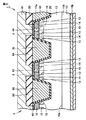
<実施の形態1>
図1は、この発明の実施の形態1に係るワイドバンドギャップ半導体装置の構成を示す断面模式図である。図1は、図5のI−I線に沿った断面図である。この実施の形態において、ワイドギャップ半導体は、炭化珪素(SiC)、窒化ガリウム(GaN)あるいはダイヤモンド(C)であり得る。
<
FIG. 1 is a schematic cross-sectional view showing a configuration of a wide bandgap semiconductor device according to
図1を参照して、この発明の実施の形態1に係るワイドバンドギャップ半導体装置1は、炭化珪素に形成された複数のMOSFET(Metal Oxide Semiconductor Field Effect Transistor)2により実現される。本実施の形態では、複数のMOSFET2は、スイッチング素子としてたとえばモータ等の誘導性負荷を駆動制御する電力変換器などに用いられる。
Referring to FIG. 1, a wide band
MOSFET2は、プレーナ型のMOSFETであって、炭化珪素単結晶基板10と、炭化珪素層11と、ゲート絶縁膜20と、ゲート電極30と、層間絶縁膜60と、ソース電極40と、ソース配線層41と、ドレイン電極50と、裏面パッド電極51とを備える。
炭化珪素単結晶基板10は、たとえばポリタイプ4Hを有する六方晶炭化珪素単結晶からなる。炭化珪素単結晶基板10は、第1の主面10aと、第2の主面10bとを有する。第2の主面10bは第1の主面10aと反対側に位置する。
Silicon carbide
炭化珪素層11は、炭化珪素からなるエピタキシャル層であり、第1の主面11aと、第2の主面11bとを有する。炭化珪素層11は、たとえばポリタイプ4Hを有する六方晶炭化珪素からなる。第2の主面11bは第1の主面11aと反対側に位置する。炭化珪素層11の第2の主面11bは、炭化珪素単結晶基板10の第1の主面10aと接する。炭化珪素層11は、ドリフト層12と、ボディ領域13と、ソース領域14と、コンタクト領域15とを有する。
ドリフト層12は、たとえば窒素などの導電型がn型(第1の導電型)である不純物(ドナー)を含むn型領域である。ドリフト層12は炭化珪素層11の第2の主面11bを含む。ドリフト層12のn型不純物濃度(第1の導電型の不純物濃度)は、炭化珪素単結晶基板10のn型不純物濃度よりも低いことが好ましい。
ボディ領域13は、たとえばアルミニウムやホウ素などの導電型がp型(第2の導電型)である不純物(アクセプタ)を含むp型領域である。
ソース領域14は、たとえばリンなどのn型不純物を含むn型領域である、ソース領域14は、ボディ領域13によってドリフト層12から隔てられるようにボディ領域13上に設けられている。ソース領域14のn型不純物濃度は、ドリフト層12のn型不純物濃度よりも高い。ソース領域14はコンタクト領域15とともに炭化珪素層11の第1の主面11aの一部を含む。
コンタクト領域15は、たとえばアルミニウムなどのp型不純物を含むp型領域である。コンタクト領域15は、ソース領域14に囲まれて設けられていると共に、ボディ領域13につながっている。コンタクト領域15のp型不純物濃度(第2の導電型の不純物濃度)は、ボディ領域13のp型不純物濃度よりも高い。
Contact
ソース領域14の下方に位置するボディ領域13の一部において開口部16が設けられる。開口部16は、ドリフト層12をソース領域14に接合させる。すなわち、開口部16内の領域の導電型はn型である。開口部16の側壁にはボディ領域13が露出している。
An
ゲート絶縁膜20は、ボディ領域13に形成されるMOSFET2のチャネルCH1と対向する位置に設けられる。ゲート絶縁膜20は、炭化珪素層11の第1の主面11aにおいて、ボディ領域13、ソース領域14およびドリフト層12に接する。ゲート絶縁膜20は、たとえば二酸化珪素からなる。
The
ゲート電極30は、ゲート絶縁膜20上に配置される。ゲート電極30は、MOSFET2のソース領域14から他方のソース領域14まで延在するように、ドリフト層12、ボディ領域13およびソース領域14と対向する。ゲート電極30は、たとえば不純物が添加されたポリシリコン、あるいはアルミニウムなどの導電体からなる。
The
層間絶縁膜60は、ゲート電極30およびゲート絶縁膜20を覆うように配置される。層間絶縁膜60は二酸化珪素からなる。層間絶縁膜60には、ソース領域14およびコンタクト領域15と重なる位置にコンタクトホールSHが形成される。コンタクトホールSHは、層間絶縁膜60およびゲート絶縁膜20を貫通するコンタクトホールである。コンタクトホールSHは、炭化珪素層11の第1の主面10aを露出させる。言い換えれば、コンタクトホールSHは、ソース領域14およびコンタクト領域15を露出させる。
ソース電極40は、コンタクトホールSHに配置されてソース領域14およびコンタクト領域15に接触する。これにより、ソース電極40は、ソース領域14およびコンタクト領域15と電気的に接続される。ソース電極40は、ソース領域14およびコンタクト領域15に対して良好な電気的接合(オーミック接合)を達成することが可能な材料、たとえばチタン、アルミニウムおよびシリコンにより構成されている。
ソース配線層41は、層間絶縁膜60上に配置される。ソース配線層41はたとえばアルミニウムからなる。ソース配線層41は、コンタクトホールSHを通じてソース電極40に電気的に接続される。
The
ドレイン電極50は、炭化珪素単結晶基板10の第2の主面10bに接触する。これにより、ドレイン電極50は炭化珪素単結晶基板10と電気的に接続されている。あるいは、ドレイン電極50は、たとえばニッケルなど、炭化珪素単結晶基板10とオーミック接合可能な他の材料からなっていてもよい。
裏面パッド電極51は、ドレイン電極50に接して配置される。裏面パッド電極51は、たとえばチタン、ニッケル、銀やそれらの合金からなる。
The
次に、図1から図4を参照して、この発明の実施の形態1に係るワイドバンドギャップ半導体装置1の動作について説明する。
Next, the operation of the wide band
MOSFET2において、ソース配線層41およびソース電極40を通じて、ソース領域14およびコンタクト領域15にソース電位VSが与えられる。ソース電位VSはたとえば接地電位である。
In
MOSFET2をオンするために、ドレイン電極50にドレイン電位VDが与えられ、ゲート電極30にゲート電位VGが与えられる。ドレイン電位VDおよびゲート電位VGはともにソース電位VSよりも高い。たとえばVD>VG>VSであるとする。ゲート電極30下のボディ領域13の表面層がn型に反転し、このn型反転層(チャネルCH1)を通じてソース領域14からチャネルCH1、ドリフト層12、炭化珪素単結晶基板10までひとつづきのn型領域でつながる。この結果、図1において実線矢印で示されるように、電流はドレイン電極50から、炭化珪素単結晶基板10、ドリフト層12、チャネルCH1およびソース領域14を通り、ソース電極40へと流れる。
To turn on the
一方、ゲート電位VGをゼロにすると、n型反転層(チャネルCH1)は消滅し、電流はゼロになる。さらに、ボディ領域13およびドリフト層12間のpn接合が逆バイアスされて主としてドリフト層12に空乏層が広がり、MOSFET2はオフ状態となる。
On the other hand, when the gate potential V G is zero, n-type inversion layer (channel CH1) disappears, the current is zero. Furthermore, the pn junction between the
本実施の形態では、図1に示されるように、開口部16において、ドリフト層12(n型領域)は、ボディ領域13(p型領域)に取り囲まれて設けられるとともに、ソース領域14に接合している。ドリフト層12、ボディ領域13、ソース領域14、炭化珪素単結晶基板10、ソース電極40およびドレイン電極50により、JFET(Junction Field Effect Transistor)3が形成される。
In the present embodiment, as shown in FIG. 1, the drift layer 12 (n-type region) is provided in the
詳細には、ボディ領域13に開口部16を設けたことにより、ソース電極40およびドレイン電極50の間には、ソース領域14、ドリフト層12および炭化珪素単結晶基板10(n型領域)からなる電流経路が形成される。この電流経路の途中には、ボディ領域13(p型領域)からなる制御電極(ゲート)が設けられている。ゲート・ドレイン間にpn接合を逆バイアスする方向の電圧が印加されると、pn接合のまわりに空乏層が広がり、電流経路を流れる電流が制御される。すなわち、MOSFET2のソース電極40およびドレイン電極50をそれぞれソース電極およびドレイン電極とし、かつ、ボディ領域13をゲートとするJFET3が形成される。ソース電極40とボディ領域13とは電気的に接続されている。よって、JFET3のゲートはソースに電気的に接続されており、ゲートにはソースと同じ電位が与えられる。
Specifically, by providing
本実施の形態において、JFET3は、ノーマリオフ型(エンハンスメント型ともいう)、すなわち閾値電圧がゼロよりも高く、ゲート電位およびソース電位が同電位のときにオフ状態となるトランジスタである。
In this embodiment, the
図2は、この発明の実施の形態1に係るワイドバンドギャップ半導体装置1の等価回路図である。以下、MOSFET2およびJFET3の各々において、ソース電位Vsを基準とするドレイン電位VDをドレイン・ソース間電圧VDSとし、ソース電位VSを基準とするゲート電位VGをゲート・ソース間電圧VGSと定義して、説明する。
FIG. 2 is an equivalent circuit diagram of the wide band
図2を参照して、MOSFET2は、ドレイン電極50と、ゲート電極30と、ソース電極40とを有する。JFET3は、ドレインがドレイン電極50に接続され、ソースがソース電極40に接続されている。JFET3のゲート(ボディ領域13)はソース電極40に接続されている。
Referring to FIG. 2,
上記のように、MOSFET2は、VDS>0の状態において、VGS>0のとき、オンされる。これにより、MOSFET2には、図1および図2の各々において実線矢印に示されるように、ドレイン電極50からソース電極40へと電流が流れる。
As described above, the
このとき、JFET3においては、ゲートにソースと同じ電位(接地電位)が与えられるとともに、ドレインにソース電位VSより高い電位が与えられている。すなわち、VDS>0かつVGS=0となっている。ノーマリオフ型のJFET3は、空乏層(図3参照)によって電流経路が遮断されるため電流が流れない。
At this time, in
図3は、ドレイン・ソース間電圧VDS>0の場合におけるワイドバンドギャップ半導体装置1の状態を模式的に示した断面図である。図3を参照して、ドレイン電位VDがソース電位VSよりも高くなるようにドレイン電極50とソース電極40との間に電圧が印加される。JFET3のゲート電位VGはソース電位VS(接地電位)と等しいため、ボディ領域13とドリフト層12間のpn接合は逆バイアスされる。これにより、ボディ領域13とドリフト層12との接合面から空乏層70が広がる。この空乏層70によりソース電極40およびドレイン電極50間の電流経路が遮断されてJFET3はオフ状態となる。
FIG. 3 is a cross-sectional view schematically showing the state of the wide band
これに対して、インバータ回路において上下アームを構成するMOSFETが両方ともオフ状態になると、ドレイン・ソース間電圧VDS<0となり、誘導性負荷に蓄積されたエネルギーにより還流電流が流れる。このとき、MOSFET2に内在するボディダイオードに還流電流が流れると、ボディダイオードによるバイポーラ動作によりSiC半導体装置の結晶劣化が進行する虞がある。さらに、ワイドバンドギャップ半導体装置においては、ボディダイオードの立上り電圧が約2.5Vと高いため、順方向の電圧降下が高くなり、導通損失を増大させるという問題がある。
On the other hand, when both MOSFETs constituting the upper and lower arms in the inverter circuit are turned off, the drain-source voltage V DS <0, and the return current flows due to the energy stored in the inductive load. At this time, if a reflux current flows through the body diode inherent in
本実施の形態では、図2および図4において点線矢印で示されるように、MOSFET2に並列接続されたJFET3に還流電流を流す。すなわち、JFET3は還流ダイオードとして機能し得る。
In this embodiment, as indicated by the dotted arrows in FIGS. 2 and 4, a reflux current is passed through
図4は、ドレイン・ソース間電圧VDS<0の場合におけるワイドバンドギャップ半導体装置1の状態を模式的に示した断面図である。図4を参照して、MOSFET2がオフ状態において、ドレイン電位VDがソース電位VSよりも低くなるようにドレイン電極50とソース電極40との間に電圧が印加される。このような状態は電力変換器の動作中に発生し得る。VDS<0の場合、ボディ領域13とドリフト層12間のpn接合は順方向にバイアスされるため、空乏層70(図3)は解消する。これにより、図4において点線矢印で示されるように、p型ゲート(ボディ領域13)に取り囲まれたn型領域(開口部16内のドリフト層12)を電流が流れる。以下の説明では、開口部16内のドリフト層12を「JFET3のチャネルCH2」とも称する。
FIG. 4 is a cross-sectional view schematically showing the state of the wide band
ここで、本実施の形態においては、MOSFET2がオフ状態のときには、JFET3をオフ状態としてJFET3の電流経路を遮断する必要がある。そのため、JFET3をノーマリオフ型としている。具体的には、JFET3のゲート電位VGおよびソース電位VSが同電位のときに、開口部16内のドリフト層12(チャネルCH2)が完全空乏化されるように、JFET3のチャネル幅を調整する。このチャネル幅とは、チャネルCH2を挟んで対向するp型領域間の距離に相当する。チャネル幅は、開口部16の開口幅で決まる。開口部16の開口幅とは、開口部16の側壁に露出するp型領域の間の最短距離である。
Here, in the present embodiment, when the
図3に示したように、ドレイン・ソース間電圧VDS>0のときには、JFET3におけるpn接合は逆バイアスされて主としてドリフト層12に空乏層70が広がる。ここで、n型領域(ドリフト層12)に形成される空乏層の厚さをXnとし、p型領域(ボディ領域13)に形成される空乏層の厚さをXpとすると、空乏層の厚さXn,Xpは次式(1),(2)でそれぞれ表わされる。
As shown in FIG. 3, when the drain-source voltage V DS > 0, the pn junction in

ここで、Naはp型領域の不純物濃度、Ndはn型領域の不純物濃度、φBはpn接合のビルトイン電位、Vbはバイアス電圧である。 Here, N a is the impurity concentration in the p-type region, N d is the impurity concentration in the n-type region, φ B is the built-in potential of the pn junction, and Vb is the bias voltage.
本実施の形態では、JFET3のチャネル幅、すなわち開口部16の開口幅をn型領域に形成される空乏層の厚さXnのほぼ2倍の大きさとする。これにより、開口部16内のドリフト層12(チャネルCH2)が完全空乏化されるため、ノーマリオフ型のJFET3を実現することができる。好ましくは、開口部16の開口幅は0.4μm以上3.0μm以下である。開口幅の下限値である0.4μmは、後述するワイドバンドギャップ半導体装置1の製造プロセスにおいて実現可能な開口幅の最小値を示している。よって、開口幅の下限値は製造プロセスに依存し、上記の値に限定されるものではない。一方、開口幅の上限値である3.0μmは、JFET3のチャネルCH2を完全空乏化することができる限界値の一例を示している。この開口幅の上限値はp型領域のアクセプタ濃度およびn型領域のドナー濃度によって決まる。
In the present embodiment, the channel width of
また、本実施の形態において、ノーマリオフ型のJFET3の閾値電圧は、ゼロよりも大きく、かつ、MOSFET2に内在するボディダイオードの立上り電圧よりも低い値とする。なお、JFET3では、ゲート・ドレイン間のpn接合を順バイアスとすることになるため、ユニポーラデバイスとして動作させるには、閾値電圧をpn接合のビルトイン電圧以下に抑える必要がある。
In the present embodiment, the threshold voltage of normally-
このような構成とすることにより、VDS<0の状態においてボディダイオードが導通状態となる前にJFET3がオンするため、JFET3を経由して還流電流が流れる。よって、ボディダイオードへの還流を抑制することができる。この結果、ボディダイオードによるバイポーラ動作によりSiC半導体装置の結晶劣化が進行するのを防止することができる。
With such a configuration, the
また、ワイドバンドギャップ半導体を材料としてMOSFET2を構成した場合、ボディダイオードの立上り電圧が約2.5Vと高いため、順方向の電圧降下が高くなり、導通損失を増大させる。本実施の形態によれば、JFET3はボディダイオードと比較して立上り電圧が低いため、順方向の電圧降下も低くなる。これにより、導通損失を低減することができる。
Further, when the
本実施の形態では、ドリフト層12のn型不純物濃度が一様であるため、JFET3のチャネルCH2におけるn型不純物濃度は、チャネルCH2から見て第2の主面11b側に配置される、残りのドリフト層12のn型不純物濃度と実質的に等しくなっている。この「n型不純物濃度が等しい」とは、チャネルCH2のn型不純物濃度が、残りのドリフト層12のn型不純物濃度に必ずしも一致している必要はなく、残りのドリフト層12のn型不純物濃度よりも高くてもよく、あるいは幾分低くてもよい。
In the present embodiment, since the n-type impurity concentration of the
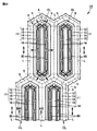
図5は、この発明の実施の形態1に係るワイドバンドギャップ半導体装置の構成を示す平面図である。図5は、炭化珪素層11の第1の主面11aの平面視におけるMOSFET2およびJFET3の構造を示している。なお、図5では、炭化珪素層11の第1の主面11a上に形成されるゲート絶縁膜20、ゲート電極30、ソース電極40、ソース配線層41および層間絶縁膜60は記載されていない。
FIG. 5 is a plan view showing the configuration of the wide band gap semiconductor device according to the first embodiment of the present invention. FIG. 5 shows structures of
図5を参照して、MOSFET2には第1の主面11aの平面視において外周形状が長軸を含む六角形状であるセルCLが互いに隣接して接触するように複数形成されている。セルCLは、炭化珪素層11に形成されたドリフト層12、ボディ領域13、ソース領域14およびコンタクト領域15を含み、さらにコンタクト領域15に接触して形成されるソース電極40(図1)を含んでいる。このように、ワイドバンドギャップ半導体装置1を第1の主面11aの平面視における外周形状が長軸を含む六角形状となるように複数に分割することにより、複数のセルCLが形成される。
Referring to FIG. 5, a plurality of cells CL whose outer peripheral shape is a hexagonal shape including a long axis in a plan view of first
セルCLの外周形状は、一組の長辺Lと当該一組の長辺Lを接続する短辺Sとから構成される六角形状となっている。長辺Lは、六角形状の長軸方向(図中の両矢印に示す方向)に沿って延びている。具体的には、長辺Lは炭化珪素の<1−100>方向に沿って延びている。複数のセルCLは、長辺Lおよび短辺Sにおいて互いに接触するように形成されている。短辺Sの長さに対する長辺Lの長さの比は1.2以上20以下であり、好ましくは、1.5以上10以下である。たとえば長辺Lの長さは200μmであり、短辺Sの長さは10μmである。なお、六角形状の長軸方向は上記<1−100>方向に限定されず、たとえば<11−20>方向などの任意の方向にすることができる。 The outer peripheral shape of the cell CL is a hexagonal shape composed of a set of long sides L and a short side S connecting the set of long sides L. The long side L extends along the long axis direction of the hexagon (the direction indicated by the double-headed arrow in the figure). Specifically, the long side L extends along the <1-100> direction of silicon carbide. The plurality of cells CL are formed so as to be in contact with each other at the long side L and the short side S. The ratio of the length of the long side L to the length of the short side S is 1.2 or more and 20 or less, preferably 1.5 or more and 10 or less. For example, the length of the long side L is 200 μm, and the length of the short side S is 10 μm. The major axis direction of the hexagonal shape is not limited to the <1-100> direction, and may be any direction such as the <11-20> direction.
コンタクト領域15の外周形状は、第1の主面11aの平面視においてセルCLの外周形状と相似形であって長軸を含む六角形状となっている。ソース領域14は、第1の主面11aの平面視においてコンタクト領域15を取り囲むように形成されており、外周形状がセルCLの外周形状と相似形であって長軸を含む六角形状となっている。ボディ領域13は、第1の主面11aの平面視においてコンタクト領域15およびソース領域14を取り囲むように形成されており、外周形状がセルCLの外周形状と相似形であって長軸を含む六角形状となっている。
The outer peripheral shape of the
セルCLの外周形状(六角形状)を構成する長辺Lおよび短辺Sは、炭化珪素の<1−100>方向に沿って延びている。セルCLに含まれるボディ領域13、ソース領域14およびコンタクト領域15の外周形状(六角形状)の各辺は、セルCLと同様に炭化珪素の<1−100>方向に沿って延びている。そのため、MOSFET2のチャネル領域(ゲート電極30下のボディ領域13)においてキャリアが移動する方向(図中の方矢印に示す方向)は、<1−100>方向に対して垂直な<11−20>方向に沿った方向となっている。このような構成とすることにより、MOSFET2の動作時において、移動度が高い方向(炭化珪素の<11−20>方向)に沿ってキャリアを移動させることができるため、MOSFET2のオン抵抗を下げることができる。
Long side L and short side S constituting the outer peripheral shape (hexagonal shape) of cell CL extend along the <1-100> direction of silicon carbide. Each side of the outer peripheral shape (hexagonal shape) of
ボディ領域13には開口部16が複数設けられている。開口部16の各々の外周形状は、たとえば四角形状となっている。開口部16の外周形状は、他の多角形、あるいは楕円形状であってもよい。開口部16はドリフト層12をソース領域14に接合させる。これにより、ボディ領域13はドリフト層12を取り囲むように形成される。そして、このドリフト層12に接触するようにソース領域14が形成されることによって、ドリフト層12にJFET3のチャネルCH2(図4参照)が形成される。
A plurality of
以上に述べたように、この発明の実施の形態1に係るワイドバンドギャップ半導体装置1では、外周形状が長軸を含む六角形状であるセルCLが複数形成され、各セルCLはソース電極40に接触するコンタクト領域15を含んでいる。これにより、外周形状が正六角形状(すなわち、長軸を含まない六角形状)であるセルが複数形成された従来の半導体装置と比較して、コンタクト領域の面積をより広げることが可能となる。この結果、コンタクト領域15とソース電極40との接触抵抗を低減できるため、MOSFET2の電気的特性を向上させることができる。
As described above, in the wide band
次に、図6を参照して、この発明の実施の形態1に係るワイドバンドギャップ半導体装置1の製造方法について説明する。この発明の実施の形態1に係るワイドバンドギャップ半導体装置1の製造方法では、まず、炭化珪素基板準備工程(S10)が実施される。この工程(S10)では、図7を参照して、たとえば4H−SiCからなるインゴット(図示せず)を切断することにより、主面10a,10bを有する炭化珪素単結晶基板10が準備される。
Next, with reference to FIG. 6, a method for manufacturing wide
次に、エピタキシャル成長層形成工程(S20)が実施される。この工程(S20)では、図7を参照して、炭化珪素単結晶基板10の第1の主面10a上にエピタキシャル成長により炭化珪素層11が形成される。
Next, an epitaxial growth layer forming step (S20) is performed. In this step (S20), referring to FIG. 7,
次に、イオン注入工程(S30)が実施される。この工程(S30)では、図8を参照して、まず、たとえばアルミニウム(Al)イオンが第1の主面11aから炭化珪素層11内に注入されることにより、炭化珪素層11内にボディ領域13が形成される。次に、たとえばリン(P)イオンがボディ領域13内に注入されることによりボディ領域13内にソース領域14が形成される。次に、たとえばAlイオンがボディ領域13内に注入されることにより、ボディ領域13内においてソース領域14に隣接するようにコンタクト領域15が形成される。そして、炭化珪素層11においてボディ領域13、ソース領域14およびコンタクト領域15のいずれもが形成されない領域がドリフト層12となる。なお、開口部16において、ドリフト層12はボディ領域13に取り囲まれて設けられる。これにより、図5に示すように、炭化珪素層11において長軸を含む六角形状からなる外周形状を有するコンタクト領域15と、コンタクト領域15を取り囲み、長軸を含む六角形状からなる外周形状を有するソース領域14と、ソース領域14およびコンタクト領域15を取り囲み、長軸を含む六角形状からなる外周形状を有するボディ領域13とが形成される。
Next, an ion implantation step (S30) is performed. In this step (S30), referring to FIG. 8, first, for example, aluminum (Al) ions are implanted into
なお、ドリフト層12に対向し開口部16を有するボディ領域13の底面部までエピタキシャル成長を行なった後に、ボディ領域13の底面部を形成するためのp型(第2の導電型)の不純物を注入し、再びエピタキシャル成長を行なってもよい。この構成によれば、ボディ領域13の底面部を形成するための不純物注入加速エネルギを下げることができ、横方向散乱が抑制されるので、精密に開口部16を形成することができる。
Note that, after epitaxial growth is performed up to the bottom surface of the
次に、活性化アニール工程(S40)が実施される。この工程(S40)では、炭化珪素層11が形成された炭化珪素単結晶基板10が加熱されることにより、炭化珪素層11内に導入された不純物が活性化する。これにより、炭化珪素層11内の不純物領域において所望のキャリアが発生する。
Next, an activation annealing step (S40) is performed. In this step (S40), impurity introduced into
次に、ゲート絶縁膜形成工程(S50)が実施される。この工程(S50)では、図9を参照して、たとえば酸素(O2)を含む雰囲気中において炭化珪素層11が形成された炭化珪素単結晶基板10を加熱することにより、第1の主面11a上に二酸化珪素(SiO2)からなるゲート絶縁膜20が形成される。
Next, a gate insulating film formation step (S50) is performed. In this step (S50), referring to FIG. 9, for example, by heating silicon carbide
次に、ゲート電極形成工程(S60)が実施される。この工程(S60)では、図9を参照して、たとえばLPCVD(Low Pressure Chemical Vapor Deposition)法により、ゲート絶縁膜20上に接触する、ポリシリコンからなるゲート電極30が形成される。
Next, a gate electrode formation step (S60) is performed. In this step (S60), referring to FIG. 9,
次に、層間絶縁膜形成工程(S70)が実施される。この工程(S70)では、図10を参照して、たとえばCVD法によりゲート絶縁膜20およびゲート電極30を覆うようにSiO2からなる層間絶縁膜60が形成される。
Next, an interlayer insulating film forming step (S70) is performed. In this step (S70), referring to FIG. 10,
次に、オーミック電極形成工程(S80)が実施される。この工程(S80)では、図11を参照して、まず、ソース電極40を形成する領域におけるゲート絶縁膜20および層間絶縁膜60がエッチングにより除去される。これにより、ソース領域14およびコンタクト領域15が露出した領域が形成される。次に、この領域にチタン、アルミニウムおよび珪素を含む合金が形成される。具体的には、上記の領域上にチタン層、アルミニウム層および珪素層をこの順で形成し、その後これらの層を加熱してチタン、アルミニウムおよび珪素を含む合金を生成する。あるいは、上記の領域上にチタン、アルミニウムおよび珪素を含む混合層を形成した後、当該混合層を加熱してチタン、アルミニウムおよび珪素を含む合金を生成することも可能である。
Next, an ohmic electrode formation step (S80) is performed. In this step (S80), referring to FIG. 11, first,
一方、炭化珪素単結晶基板10の第2の主面10b上においてニッケルからなる膜が形成される。その後、炭化珪素単結晶基板10が加熱されることにより、ニッケルからなる膜の少なくとも一部がシリサイド化する。これにより、炭化珪素層11の第1の主面11aおよび炭化珪素単結晶基板10の第2の主面10b上においてソース電極40およびドレイン電極50がそれぞれ形成される。
On the other hand, a film made of nickel is formed on second
次に、配線形成工程(S90)が実施される。この工程(S90)では、たとえば蒸着法により、Alや金(Au)などの導電体からなるソース配線層41がソース電極40および層間絶縁膜60を覆うように形成される。また、ソース配線層41と同様にAlやAuなどからなる裏面パッド電極51がドレイン電極50を覆うように形成される。上記工程(S10)〜(S90)が実施されることにより、MOSFET2とJFET3とを集積化したワイドバンドギャップ半導体装置1(図1)が製造される。
Next, a wiring formation step (S90) is performed. In this step (S90), the
この発明の実施の形態1によれば、還流ダイオードとして機能し得るJFETを、1つのMOSFETのセルに集積化させることができる。これにより、還流ダイオードを設けるためにトランジスタセルのサイズ、すなわち、半導体チップの実装面積が増大するのを抑えることができる。この結果、電力変換装置のような、トランジスタ素子と還流ダイオードとを含む回路を、より小型かつ簡素な構成で実現することができる。したがって、炭化珪素に代表されるワイドバンドギャップ半導体を材料として構成されたパワー半導体装置においては、半導体チップの小型化が妨げられることがない。 According to the first embodiment of the present invention, a JFET that can function as a freewheeling diode can be integrated in a single MOSFET cell. Thus, an increase in the size of the transistor cell, that is, the mounting area of the semiconductor chip, due to the provision of the free-wheeling diode can be suppressed. As a result, a circuit including a transistor element and a free-wheeling diode, such as a power conversion device, can be realized with a smaller and simpler configuration. Therefore, in a power semiconductor device configured with a wide band gap semiconductor typified by silicon carbide as a material, downsizing of the semiconductor chip is not hindered.
また、この発明の実施の形態1によれば、JFETをMOSFETの製造工程を大きく変更することなく製造することができるため、トランジスタ素子と還流ダイオードとを含む回路を簡素なプロセスで製造することができる。 Further, according to the first embodiment of the present invention, a JFET can be manufactured without greatly changing the MOSFET manufacturing process, and therefore a circuit including a transistor element and a free wheel diode can be manufactured by a simple process. it can.
<実施の形態2>
図12は、この発明の実施の形態2に係るワイドバンドギャップ半導体装置の構成を示す断面模式図である。図12を参照して、この発明の実施の形態2に係るワイドバンドギャップ半導体装置1Aにおいて、炭化珪素層11は、p型埋込領域80(第1の不純物領域)をさらに含む。p型埋込領域80は、たとえばアルミニウムやホウ素などの不純物(アクセプタ)を含むp型領域である。p型埋込領域80は、ボディ領域13よりも第2の主面11b側に位置するようにドリフト層12の内部に埋め込まれている。すなわち、p型埋込領域80は、ドリフト層12によってボディ領域13から隔てられている。p型埋込領域80は、エピタキシャル成長層形成工程(図6のS20)において、炭化珪素単結晶基板10上に炭化珪素層11を形成する過程で、注入マスクを用いたアクセプタイオン(第2の導電型を付与するための不純物イオン)の注入により形成することができる。
<
FIG. 12 is a schematic cross-sectional view showing the configuration of the wide band gap semiconductor device according to the second embodiment of the present invention. Referring to FIG. 12, in wide band
なお上記以外の構成については、上述した実施の形態1の構成とほぼ同じであるため、同一または対応する要素について同一の符号を付し、その説明を繰り返さない。 Since the configuration other than the above is substantially the same as the configuration of the first embodiment described above, the same or corresponding elements are denoted by the same reference numerals, and description thereof will not be repeated.
この発明の実施の形態2によれば、上記の実施の形態1と同様の効果を得ることができる。さらにこの発明の実施の形態2によれば、以下に述べるように、p型埋込領域80によって、ソース電極40の直下に位置するドリフト層12(JFET3のチャネルに相当)にかかる電界が緩和される。これにより、JFET3のオフ時におけるリーク電流の発生を抑制できるため、JFET3の耐圧への影響を回避することができる。
According to the second embodiment of the present invention, the same effect as in the first embodiment can be obtained. Furthermore, according to the second embodiment of the present invention, the electric field applied to drift layer 12 (corresponding to the channel of JFET 3) located immediately below
図13は、ドレイン・ソース間電圧VDS>0場合におけるワイドバンドギャップ半導体装置1Aの状態を模式的に示した断面図である。図13において、p型埋込領域80は、ソース配線層41と電気的に接続されている。したがって、埋込領域80にはソース電極40に与えられる電位VS(接地電位)と同じ電位が与えられる。すなわち、埋込領域80は、ボディ領域13およびコンタクト領域15と同じ電位(接地電位)となっている。
FIG. 13 is a cross-sectional view schematically showing the state of the wide band
図13を参照して、p型埋込領域80とドリフト層12との間のpn接合には逆バイアス電圧が印加されているため、p型埋込領域80およびドリフト層12の接合面から、p型埋込領域80側およびドリフト層12側に空乏層が広がる。このp型埋込領域80およびドリフト層12の接合面からドリフト層12側に延びる空乏層と、ボディ領域13およびドリフト層12の接合面からドリフト層12側に延びる空乏層(図3参照)とによって、図13に示すようにボディ領域13と炭化珪素層11の第2の主面11bとの間に、十分な長さを有する空乏層72が形成され得る。これにより、ドレイン電極50およびソース電極40間の電圧について、p型埋込領域80と炭化珪素層11の第2の主面11bとの間で負担される割合が高められる。言い換えれば、p型埋込領域80よりも浅い部分(図13におけるより上方の部分)で負担される電圧が軽減される。これにより、p型埋込領域80よりも浅い部分での電界強度を小さくすることができる。言い換えれば、電界集中が生じやすい、ソース領域14直下のドリフト層12の電界強度を小さくすることができる。これにより、リーク電流がドレイン電極50からソース電極40へ流れるのが抑制されるため、ドレイン電極50およびソース電極40間に高い電圧を印加することができる。つまり、JFET3の耐圧への影響を回避できるため、JFET3の有する高い耐圧を維持することができる。
Referring to FIG. 13, since a reverse bias voltage is applied to the pn junction between p type buried
本実施の形態では、p型埋込領域80は、ドリフト層12の不純物濃度よりも高い不純物濃度を有することが好ましい。p型埋込領域80の不純物濃度をドリフト層12の不純物濃度よりも十分に高くすることにより、ドレイン電位VDとソース電位VSとの電位差が高まった場合に、p型埋込領域80から炭化珪素層11の第2の主面11bへ空乏層が十分に延びる前にp型埋込領域80が完全に空乏化してしまうことが防止される。これにより、p型埋込領域80と第2の主面11bとの間に、十分な長さを有する空乏層が形成されるため、リーク電流が流れるのを確実に抑制することができる。
In the present embodiment, p type buried
一方、p型埋込領域80の不純物濃度をドリフト層12の不純物濃度に対して十分に高くしない場合には、p型埋込領域80が完全に空乏化される。この場合には、JFET3の寄生容量を低減することができる。
On the other hand, when the impurity concentration of p type buried
図13に示したワイドバンドギャップ半導体装置1Aにおいて、p型埋込領域80がソース電極40に電気的に接続されることにより、p型埋込領域80とボディ領域13とが同電位となっている。p型埋込領域80の電位が固定されているため、ワイドバンドギャップ半導体装置1Aの動作を安定化させることができる。さらに、p型埋込領域80がソース電極40に接続される結果、正孔をp型埋込領域80に効果的に注入することができる。したがって、JFET3の応答速度を高めることができる。
In the wide band
変形例として、p型埋込領域80の電位を浮遊電位(フローティング)とした構造が用いられてもよい。これによれば、ドレイン・ソース間電圧VDS>0のとき、p型埋込領域80の電位は、ボディ領域13の電位より高く、かつドレイン電位VDよりも低い電位となる。したがって、p型埋込領域80とドリフト層12との間の電位差が、ボディ領域13の電位とドリフト層12の電位との間の電位差よりも小さくなる。これにより、p型埋込領域80とボディ領域13とを同電位とする場合(図13)と比較して、ボディ領域13とドリフト層12との接合面からドリフト層12側に、より長く空乏層を延ばすことができる。この結果、JFET3の耐圧を確保することができる。
As a modification, a structure in which the potential of the p-type buried
上記のp型埋込領域80の電位をフローティングとした構造においては、p型埋込領域80は、ボディ領域13からp型埋込領域80にキャリア(正孔)を供給できるように、ボディ領域13の近傍に設けられることが好ましい。具体的には、VDS<0のとき、JFET3に電流が流れる。この場合、ドレイン電極50から注入された電子がソース電極40へと移動可能である。これにより、ドリフト層12側に形成された空乏層72を縮小(解消)することができる。一方、ソース電極40からボディ領域13に正孔が注入されることで、ボディ領域13の空乏化を解消することができる。本実施の形態ではさらに、ボディ領域13からp型埋込領域80に正孔が注入されることにより、p型埋込領域80の空乏化を短時間で解消することができる。このようにp型埋込領域80に対する正孔の注入を円滑に行なうことができるため、JFET3の応答速度を向上させることができる。
In the structure in which the potential of the p-type buried
好ましくは、炭化珪素層11の厚さ方向(図12の縦方向)におけるボディ領域13とp型埋込領域80との間の距離は5μm以下である。この「距離が5μm以下」とは、たとえばボディ領域13とp型埋込領域80との間の最短の距離が5μm以下であってもよい。逆に、ボディ領域13とp型埋込領域80との間の最大の距離が5μm以下であってもよい。たとえば、P. A. Ivanov 他6名による「High Hole lifetime (3.8μm) in 4H-SiC diodes with 5.5kV blocking voltage」、Electronics Letters、1999年、第35巻、第16号、1382頁〜1383頁によれば、5.5kV耐圧の4H−SiCダイオードにおける正孔の寿命が0.6〜3.8μs(300〜550K)、正孔の拡散長が16〜22μm(不純物濃度:6×1014cm−3)である。ボディ領域13とp型埋込領域80との間の距離を5μm以下とすることにより、ボディ領域13からp型埋込領域80へ正孔を注入することが可能になる。これにより、p型埋込領域80の空乏化の解消および電位回復を達成することができる。
Preferably, the distance between
より好ましくは、炭化珪素層11の厚さ方向におけるボディ領域13とp型埋込領域80との間の距離は2μm以下である。上記文献から、ボディ領域13とp型埋込領域80との間の距離を2μm以下とすることにより、数十ns(ナノ秒)以下の時間でp型埋込領域80の空乏化の解消および電位回復を達成することが期待できる。したがって、高速の応答が可能なワイドバンドギャップ半導体装置を実現することができる。
More preferably, the distance between
また、本実施の形態においては、VDS>0の状態において、ボディ領域13およびp型埋込領域80の各々から炭化珪素層11の第2の主面11b側へ延びる空乏層が形成される。すなわち、ボディ領域13に加えてp型埋込領域80もJFET3のゲートとなり得る。このため、上記の実施の形態1と比較して、リーク電流を遮断するためにボディ領域13が負担すべき空乏層の大きさを軽減することができる。したがって、変形例として、JFET3を、ノーマリオン型(ディプレッション型ともいう)、すなわち閾値電圧がゼロよりも低く、ゲート電位およびソース電位が同電位のときのオン状態となるトランジスタとすることができる。図14は、ドレイン・ソース間電圧VDS>0の場合におけるワイドバンドギャップ半導体装置1Aの変形例の状態を模式的に示した断面図である。図14に示すワイドバンドギャップ半導体装置1Aの変形例において、JFET3はノーマリオン型のトランジスタである。したがって、ゲート電位VGおよびソース電位VSが同電位の状態においてJFET3はオン状態となり、チャネルが完全に空乏化されない。このような場合でも、ドレイン電圧の上昇につれてp型埋込領域80から第2の主面11bへ延びる空乏層74によってリーク電流を遮断することができる。還流ダイオードにノーマリオン型のJFETを用いることにより、ノーマリオフ型のJFETを用いる場合と比較して、還流ダイオードにおける順方向の電圧降下を小さくすることができる。これにより、JFETの導通損失を低減することができる。
In the present embodiment, a depletion layer extending from each of
以下、ワイドバンドギャップ半導体装置1Aにおけるp型埋込領域80の配置位置について、図15から図24を参照して詳細に説明する。
Hereinafter, the arrangement position of the p-type buried
(第1の配置例)
図15は、p型埋込領域80の第1の配置例を示す平面図である。図16は、図15のXVI−XVI線に沿った断面図である。図15は、炭化珪素層11の第1の主面11aの平面視におけるMOSFET2およびJFET3の構造を示している。なお、図15では、炭化珪素層11の第1の主面11a上に形成されるゲート絶縁膜20、ゲート電極30、ソース電極40、ソース配線層41および層間絶縁膜60は記載されていない。
(First arrangement example)
FIG. 15 is a plan view showing a first arrangement example of the p-type buried
図15および図16を参照して、p型埋込領域80は、第1の主面11aの平面視において、開口部16内に配置される。詳細には、第1の主面11aの平面視において、p型埋込領域80とボディ領域13との間には間隙が設けられている。これにより、p型埋込領域80は、第1の主面11aの平面視において、ボディ領域13と重ならないように配置される。
Referring to FIGS. 15 and 16, p type buried
ドレイン・ソース間電圧VDS<0の場合、JFET3がオン状態となり電流がソース電極40からドレイン電極50へ流れる。第1の配置例によれば、この電流の経路がp型埋込領域80によって狭められるのが軽減されるため、JFET3のオン抵抗を低減することができる。
When the drain-source voltage V DS <0, the
p型埋込領域80の外周形状は、第1の主面11aの平面視において、開口部16の外周形状と相似形であって長軸を含む四角形状となっている。p型埋込形状80の外周形状は、他の多角形、あるいは楕円形状であってもよい。
The outer peripheral shape of the p-type embedded
ボディ領域13は、第1の主面11aの平面視において、p型埋込領域80を取り囲むように形成されており、外周形状がセルCLの外周形状と相似形であって長軸を含む六角形状となっている。p型埋込領域80の外周形状をなす四角形状の長軸は、セルCLと同様に炭化珪素の<1−100>方向(図中の両矢印に示す方向)に沿って延びている。図16に示される距離d1は、<1−100>方向に対して垂直な<11−20>方向における、ボディ領域13と、そのボディ領域13に隣接するp型埋込領域80との間の距離である。
(第2の配置例)
図17は、p型埋込領域80の第2の配置例を示す平面図である。図16は、図17のXVI−XVI線に沿った断面図である。図17は、図15と同様に炭化珪素層11の第1の主面11aの平面視におけるMOSFET2およびJFET3の構造を示している。なお、図17では、炭化珪素層11の第1の主面11a上に形成されるゲート絶縁膜20、ゲート電極30、ソース電極40、ソース配線層41および層間絶縁膜60は記載されていない。
(Second arrangement example)
FIG. 17 is a plan view showing a second arrangement example of the p-type buried
図17を参照して、第2の配置例は、図15に示した第1の配置例と比較して、開口部16の各々に四角形状の外周形状を有するp型埋込領域80が複数形成されている点において異なっている。第2の配置例では、複数のp型埋込領域80の各々は、開口部16内に位置するように配置される。p型埋込領域80の各々の外周形状は四角形状以外の形状であってもよい。
Referring to FIG. 17, the second arrangement example has a plurality of p-type buried
具体的には、第1の主面11aの平面視において、四角形状のp型埋込領域80は、1つの開口部16内に複数(たとえば3個)形成されている。複数のp型埋込領域80は、セルCLの外周形状である六角形状の長軸方向に沿って間隔をおいて(等間隔に)形成されている。
Specifically, a plurality of (for example, three) rectangular p-type buried
複数の開口部16の各々において、p型埋込領域80を複数形成しても、上記第1の配置例と同様の効果を奏する。なお、p型埋込領域80の数は、図17に示すように各開口部16において3個ずつであってもよいが特に限定されない。
Even if a plurality of p-type buried
第2の配置例では、第1の主面11aの平面視において、開口部16内に複数のp型埋込領域80を互いに間隔をおいて並べて形成する。これにより、図15に示した第1の配置例と比較して、JFET3を流れる電流の経路が狭められるのをさらに軽減することができる。よって、JFET3のオン抵抗を、より一層低減することが可能となる。
In the second arrangement example, a plurality of p-type buried
(第3の配置例)
図18は、p型埋込領域80の第3の配置例を示す平面図である。図19は、図18のXIX−XIX線に沿った断面図である。図18は、図15と同様に炭化珪素層11の第1の主面11aの平面視におけるMOSFET2およびJFET3の構造を示している。なお、図18では、炭化珪素層11の第1の主面11a上に形成されるゲート絶縁膜20、ゲート電極30、ソース電極40、ソース配線層41および層間絶縁膜60は記載されていない。
(Third arrangement example)
FIG. 18 is a plan view showing a third arrangement example of the p-type buried
図18および図19を参照して、p型埋込領域80は、第1の主面11aの平面視において、p型埋込領域80の一部分がボディ領域13に重なるように配置される。言い換えれば、p型埋込領域80の一部分が開口部16内に配置される。詳細には、第1の主面11aの平面視において、p型埋込領域80とボディ領域13との間には重なり部分が設けられている。図19に示される距離d2は、炭化珪素の<1−100>方向に対して垂直な<11−20>方向における、ボディ領域13と、そのボディ領域13に隣接するp型埋込領域80との重なり部分の距離である。
Referring to FIGS. 18 and 19, p type buried
図13および図14に示したように、ドレイン・ソース間電圧VDS>0の場合、ボディ領域13およびドリフト層12の接合面から第2の主面11bに向かって空乏層が延びるとともに、p型埋込領域80およびドリフト層12の接合面から第2の主面11bに向かって空乏層が延びる。第3の配置例によれば、これら2つの空乏層をつながりやすくすることができる。これにより、ソース電極40の直下に位置するドリフト層12(JFET3のチャネル)にかかる電界を、より一層緩和することができる。この結果、リーク電流の発生をより確実に抑制できるため、JFET3の耐圧を維持することができる。
As shown in FIGS. 13 and 14, when the drain-source voltage V DS > 0, the depletion layer extends from the junction surface of the
さらに、第3の配置例によれば、p型埋込領域80の電位をフローティングとした構造において、ボディ領域13からp型埋込領域80にキャリア(正孔)を供給しやすくなる。ボディ領域13からp型埋込領域80に効果的に正孔が注入されることにより、p型埋込領域80の空乏化を短時間で解消することができる。これにより、JFET3の応答速度をより一層向上させることができる。
Furthermore, according to the third arrangement example, carriers (holes) can be easily supplied from the
図20は、第3の配置例が適用されたワイドバンドギャップ半導体装置1Aを示す平面図である。図20は、炭化珪素層11の第1の主面11aの平面視におけるMOSFET2およびJFET3の構造を示している。なお、図20では、炭化珪素層11の第1の主面11a上に形成されるゲート絶縁膜20、ゲート電極30、ソース電極40、ソース配線層41および層間絶縁膜60は記載されていない。
FIG. 20 is a plan view showing a wide band
図20を参照して、セルCLに含まれるボディ領域13の外周形状の各辺は、六角形状の長軸方向(炭化珪素の<1−100>方向(図中の両矢印に示す方向))に沿って延びている。これに対して、p型埋込領域80は、<1−100>方向に対して垂直な方向(図中の片矢印に示す方向)に沿って延びている。そして、p型埋込領域80は、<1−100>方向に沿って複数並べて配置される。これにより、ボディ領域13とp型埋込領域80とは、第1の主面11aの平面視において互いに交差するように配置される。
Referring to FIG. 20, each side of the outer peripheral shape of
上記の構成において、ボディ領域13とp型埋込領域80との交差部分は、平面視におけるボディ領域13とp型埋込領域80との間の重なり部分となる。したがって、上述したように、VDS>0の状態において、ボディ領域13およびドリフト層12の接合面から第2の主面11bに向かって延びる空乏層と、p型埋込領域80およびドリフト層12の接合面から第2の主面11bに向かって延びる空乏層とがつながりやすくなる。これにより、リーク電流の発生をより確実に抑制できるため、JFET3の耐圧を高めることができる。
In the above configuration, the intersection between the
また、p型埋込領域80の電位をフローティングとした構造においては、VDS<0のときに、ボディ領域13からp型埋込領域80にキャリア(正孔)を効果的に注入することができる。これにより、JFET3の応答速度をより一層向上させることができる。
In the structure in which the potential of the p-type buried
さらに、第1の主面11aの平面視において、複数のp型埋込領域80は、各セルCLの開口部16内に互いに間隔をおいて並べて配置されるため、JFET3を流れる電流の経路が狭められるのを軽減することができる。よって、JFET3のオン抵抗を低減することができる。
Furthermore, in the plan view of the first
(第4の配置例)
図21は、p型埋込領域80の第4の配置例を示す断面図である。図21を参照して、第4の配置例は、上記第3の配置例と比較して、p型埋込領域80に、ドリフト層12が厚さ方向に沿ってつながるように貫通部81が設けられている点において異なっている。貫通部81は、たとえばp型埋込領域80に設けられた貫通孔である。なお、第4の配置例においては、貫通部81の周りをp型埋込領域80が完全に取り囲んでいる必要はない。貫通部81とは、厚さ方向に垂直な面に沿って広がるp型埋込領域80がこの面(すなわち平面視において)パターンを有する場合における、パターンの非形成部である。たとえば、非形成部を完全に取り囲むことで非形成部を貫通孔として構成してもよく、あるいは形成部が島状に存在することで非形成部を網状に構成してもよい。
(Fourth arrangement example)
FIG. 21 is a cross-sectional view showing a fourth arrangement example of the p-type buried
貫通部81の開口幅は、VDS>0のときに貫通部81内のドリフト層12が完全に空乏化されるように調整される。貫通部81の開口幅とは、貫通部81の側壁に露出するp型埋込領域80の間の最短距離である。
The opening width of the penetrating
第4の配置例によれば、ドレイン・ソース間電圧VDS<0のとき、貫通部81中に位置するドリフト層12を通ってJFET3を流れる電流の経路が形成され得る。このため、上記第3の配置例のように、第1の主面11aの平面視において、p型埋込領域80の一部分がボディ領域13に重なるように配置されている場合においても、JFET3の電流経路がp型埋込領域80によって狭められるのを軽減することができる。これにより、JFET3の高耐圧を維持しつつ、JFET3のオン抵抗を下げることができる。
According to the fourth arrangement example, when the drain-source voltage V DS <0, a path of current flowing through the
図22は、p型埋込領域の第4の配置例が適用されたワイドバンドギャップ半導体装置1Aを示す平面図である。図22は、炭化珪素層11の第1の主面11aの平面視におけるMOSFET2およびJFET3の構造を示している。なお、図22では、炭化珪素層11の第1の主面11a上に形成されるゲート絶縁膜20、ゲート電極30、ソース電極40、ソース配線層41および層間絶縁膜60は記載されていない。
FIG. 22 is a plan view showing a wide band
図22を参照して、p型埋込領域80において、貫通部81は、第1の主面11aの平面視において開口部16と重なるように形成されている。したがって、p型埋込領域80は、第1の主面11aの平面視において、ボディ領域13と重なるように配置されている。
Referring to FIG. 22, in p type buried
(第5の配置例)
図23は、p型埋込領域80の第5の配置例を示す断面図である。図23を参照して、第5の配置例は、上記第1から第4の配置例と比較して、炭化珪素層11がn型埋込領域82(第2の不純物領域)をさらに含む点において異なっている。
(Fifth arrangement example)
FIG. 23 is a cross-sectional view showing a fifth arrangement example of the p-type buried
n型埋込領域82は、たとえば窒素などの不純物(ドナー)を含むn型領域である。n型埋込領域82は、ボディ領域13よりも第2の主面11b側に位置するようにドリフト層12の内部に埋め込まれている。n型埋込領域82は、エピタキシャル成長層形成工程(図6のS20)において、炭化珪素単結晶基板10上に炭化珪素層11を形成する過程で、注入マスクを用いたドナーイオン(第1の導電型を付与するための不純物イオン)の注入により形成することができる。
N-type buried
n型埋込領域82は、ドリフト層12の不純物濃度よりも高い不純物濃度を有する。好ましくは、n型埋込領域82は、ドリフト層12の不純物濃度の1.5倍以上の不純物濃度を有する。したがって、n型不純物濃度に基づいて、ドリフト層12内のn型埋込領域82を特定することができる。たとえば走査型静電容量顕微鏡(SCM)を用いて、炭化珪素層11の厚さ方向に沿ってn型不純物濃度を解析することによって、n型埋込領域82を特定することができる。
N type buried
n型埋込領域82は、第1の主面11aの平面視において、p型埋込領域80に並設される。図23に示すように、たとえば、n型埋込領域82は、第1の主面11aの平面視において、p型埋込領域80を挟んで両側に配置される。なお、図23では、p型埋込領域80を挟んで2つのn型埋込領域82が配置されているが、第1の主面11aの平面視において、この2つのn型埋込領域82がp型埋込領域80の周りを取り囲むようにつながることによって実質的に単一のn型埋込領域82となっていてもよい。また、n型埋込領域82はp型埋込領域80と接していてもよい。
N-type buried
第5の配置例によれば、n型埋込領域82によって、ドレイン・ソース間電圧VDS<0の場合におけるJFET3のオン抵抗を低減することができる。これは、p型埋込領域80からドリフト層12中への厚さ方向に垂直な方向(図23の横方向)の空乏化の進展が、n型埋込領域82によって抑制されるためである。したがって、JFET3の高耐圧を維持しつつ、JFET3のオン抵抗を下げることができる。
According to the fifth arrangement example, the n-type buried
p型埋込領域80は、n型埋込領域82の不純物濃度よりも高い不純物濃度を有することが好ましい。ドレイン・ソース間電圧VDS>0の場合に、p型埋込領域80から第2の主面11bへ空乏層が十分に延びる前にp型埋込領域80が完全に空乏化してしまうのを防止するためである。これにより、p型埋込領域80と第2の主面11bとの間に、十分な長さを有する空乏層を形成することができるため、JFET3の耐圧がより高められる。
P type buried
図24は、図23に示すワイドバンドギャップ半導体装置1Aの断面図の一部を拡大した部分拡大図である。図24を参照して、n型埋込領域82のトップラインは、p型埋込領域80のトップラインTLよりも厚さ方向において第1の主面11a側に位置することが好ましい。
24 is a partially enlarged view of a part of the cross-sectional view of the wide band
n型埋込領域82のトップラインは、炭化珪素層11の第1の主面11aから炭化珪素層11の厚さ方向に沿ったn型不純物濃度のプロファイルにおいて、n型不純物濃度の急峻な上昇が生じる位置とすることができる。p型埋込領域80のトップラインTLとは、p型埋込領域80の上側の接合面の位置を示す仮想的な線である。なお、「p型埋込領域80の上側の接合面」とは、p型埋込領域80とドリフト層12との接合面のうち、炭化珪素層11の第1の主面11aに対向するように形成された接合面であり、かつ、炭化珪素単結晶基板10の第2の主面10bよりも第1の主面11aに位置にある接合面である。
The top line of n-type buried
n型埋込領域82は、トップラインTLを含むようにドリフト層12の内部に配置される。詳細には、n型埋込領域82は、第1の主面11a側に位置する第1の端部と、第2の主面11b側に位置する第2の端部とを有する。p型埋込領域80のトップラインTLは、第1の主面11aから第2の主面11bへと向かう深さ方向における、n型埋込領域82の第1の端部の位置から、n型埋込領域82の第2の端部の位置までの範囲内に位置する。
N type buried
図24において、p型埋込領域80は、第2の主面11bに向かってn型埋込領域82よりも延びている。これにより、VDS>0の状態において、p型埋込領域80から第2の主面11bへと向かう方向(図24の下方向)の空乏化の進展が、n型埋込領域82によって抑制されるのを防止することができる。よって、p型埋込領域80と第2の主面11bとの間に、十分な長さを有する空乏層を形成することができるため、JFET3の耐圧が更に高められる。
In FIG. 24, p-type buried
n型埋込領域82は、第1の主面11aに向かってp型埋込領域80よりも延びている。VDS<0の状態において、p型埋込領域80から第1の主面11aへと向かう方向(図24の上方向)へ空乏層が延びる。このとき、空乏層は厚さ方向に垂直な方向(図24の横方向)にも広がり得る。この空乏層の横方向の広がりを、n型埋込領域82によって抑制することができる。この結果、JFET3の電流流路の狭まりを軽減できるため、JFET3のオン抵抗を、より一層低減することができる。
N type buried
なお、上述した実施の形態1および2では、縦型のプレーナ型MOSFETを一例として説明したが、MOFETの構造はこれに限定されるものではない。たとえばこの発明に係るワイドバンドギャップ半導体装置は、トレンチ型MOSFETにも適用することが可能である。図25は、本発明の実施の形態1に係るワイドバンドギャップ半導体装置の他の構成例を示す断面模式図である。図25を参照して、炭化珪素層11の第2の主面11aには(ゲート)トレンチTRが設けられている。トレンチTRは、側壁部SWおよび底部BTからなる。側壁部SWは、第1の主面11aからソース領域14およびボディ領域13を貫通してドリフト層12に至っている。底部BTは、側壁部SWと接し、かつドリフト層12に位置している。側壁部SWは、ボディ領域13上においてMOSFET2のチャネル面を含む。側壁部SWは、炭化珪素層11の第1の主面11aに対して傾斜している。断面視(第1の主面11bに平行な視野)において、トレンチTRは開口に向かってテーパ状に広がっている。好ましくは、側壁部SWは特殊面を含む。特殊面とは、面方位{0−33−8}を有する第1の面を含む面である。より好ましくは、特殊面は、第1の面を微視的に含み、さらに面方位{0−11−1}を有する第2の面を微視的に含む。さらに好ましくは、第1の面および第2の面は、面方位{0−11−2}を有する複合面を含む。また、特殊面は、{000−1}面に対して、巨視的に62°±10°のオフ角を有する面である。
In the first and second embodiments described above, the vertical planar MOSFET has been described as an example, but the structure of the MOFET is not limited to this. For example, the wide band gap semiconductor device according to the present invention can be applied to a trench MOSFET. FIG. 25 is a schematic cross-sectional view showing another configuration example of the wide band gap semiconductor device according to the first embodiment of the present invention. Referring to FIG. 25, second
なお、トレンチTRの側壁部SWは、炭化珪素層11の第1の主面11aに対して垂直であってもよい。
Note that sidewall portion SW of trench TR may be perpendicular to first
ゲート絶縁膜20は、トレンチTRの側壁部SWおよび底部BTを覆っている。ゲート電極30はゲート絶縁膜20上に設けられる。すなわち、ゲート電極30は、ゲート絶縁膜20に接し、トレンチTRの内部に設けられている。
図25に示すトレンチ型MOSFETにおいても、開口部16の下のドリフト層12をチャネルとするJFETが形成されている。したがって、上述した効果と同様の効果を得ることができる。
Also in the trench MOSFET shown in FIG. 25, a JFET having the
なお、上記実施の形態1および2では、ワイドバンドギャップ半導体装置に配置されるトランジスタとしてMOSFETを例示した。しかしながら、この発明の実施の形態に係るワイドバンドギャップ半導体装置に配置されるトランジスタ素子は、たとえばIGBT(Insulated Gate Bipolar Transistor)などであってもよい。 In the first and second embodiments, the MOSFET is exemplified as the transistor disposed in the wide band gap semiconductor device. However, the transistor element arranged in the wide band gap semiconductor device according to the embodiment of the present invention may be, for example, an IGBT (Insulated Gate Bipolar Transistor).
また、上記実施の形態1および2では、炭化珪素層11は、全体としてn型の炭化珪素の層である。すなわち、上記実施の形態1および2では、炭化珪素層11の導電型である第1の導電型はn型であり、ボディ領域13の導電型である第2の導電型はp型である。p型の領域をn型の炭化珪素層に形成することによって、ワイドバンドギャップ半導体装置の製造し易さを向上させることができる。しかしながら第1の導電型がp型であり、かつ第2の導電型がn型であってもよい。
In the first and second embodiments,
今回開示された実施の形態はすべての点で例示であって、制限的なものではないと考えられるべきである。本発明の範囲は上記した説明ではなくて特許請求の範囲によって示され、特許請求の範囲と均等の意味、および範囲内でのすべての変更が含まれることが意図される。 The embodiment disclosed this time is to be considered as illustrative in all points and not restrictive. The scope of the present invention is defined by the terms of the claims, rather than the description above, and is intended to include any modifications within the scope and meaning equivalent to the terms of the claims.
1,1A ワイドバンドギャップ半導体装置
2 MOSFET
3 JFET
10 炭化珪素単結晶基板
11 炭化珪素層
12 ドリフト層
13 ボディ領域
14 ソース領域
15 コンタクト領域
16 開口部
20 ゲート絶縁膜
30 ゲート電極
40 ソース電極
41 ソース配線層
50 ドレイン電極
51 裏面パッド電極
60 層間絶縁膜
70,72,74 空乏層
80 p型埋込領域
81 貫通部
82 n型埋込領域
CH1,CH2 チャネル
CL セル
1,1A Wide band
3 JFET
DESCRIPTION OF
Claims (23)
第1の主面と、前記第1の主面に対して反対側に位置する第2の主面とを有するワイドバンドギャップ半導体層を備え、
前記ワイドバンドギャップ半導体層は、
第1の導電型を有し、前記第2の主面を含むドリフト層と、
前記ドリフト層に設けられて、前記第1の導電型とは異なる第2の導電型を有するボディ領域と、
前記ドリフト層から隔てられるように前記ボディ領域に設けられて、前記第1の主面の一部を含み、前記第1の導電型を有するソース領域と、
前記ボディ領域に設けられ、前記ソース領域と接するように配置されて、前記第2の導電型を有するコンタクト領域とを含み、
前記ボディ領域には、前記ドリフト層を前記ソース領域に接合させる開口部が設けられ、
前記ワイドバンドギャップ半導体装置は、
前記第1の主面において、前記ボディ領域、前記ソース領域および前記ドリフト領域に接するゲート絶縁膜と、
前記ゲート絶縁膜上に設けられたゲート電極と、
前記ソース領域および前記コンタクト領域に電気的に接続されるソース電極と、
前記第2の主面に電気的に接続されるドレイン電極とをさらに備える、ワイドバンドギャップ半導体装置。 A wide band gap semiconductor device,
A wide band gap semiconductor layer having a first main surface and a second main surface located on the opposite side to the first main surface;
The wide band gap semiconductor layer is
A drift layer having a first conductivity type and including the second main surface;
A body region provided in the drift layer and having a second conductivity type different from the first conductivity type;
A source region provided in the body region so as to be separated from the drift layer, including a part of the first main surface, and having the first conductivity type;
A contact region provided in the body region, disposed in contact with the source region, and having the second conductivity type;
The body region is provided with an opening for joining the drift layer to the source region,
The wide band gap semiconductor device is:
A gate insulating film in contact with the body region, the source region, and the drift region in the first main surface;
A gate electrode provided on the gate insulating film;
A source electrode electrically connected to the source region and the contact region;
A wide band gap semiconductor device further comprising a drain electrode electrically connected to the second main surface.
前記開口部内に配置され、前記ボディ領域に取り囲まれた第1の領域と、
前記第1の領域から見て前記第2の主面側に配置される第2の領域とを含み、
前記第1の領域の不純物濃度は、前記第2の領域の不純物濃度と等しい、もしくは前記第2の領域の不純物濃度よりも高い、請求項1に記載のワイドバンドギャップ半導体装置。 The drift layer is
A first region disposed within the opening and surrounded by the body region;
A second region disposed on the second main surface side when viewed from the first region,
2. The wide band gap semiconductor device according to claim 1, wherein an impurity concentration of the first region is equal to an impurity concentration of the second region or higher than an impurity concentration of the second region.
前記第2の導電型は、p型である、請求項1から請求項3のいずれか1項に記載のワイドバンドギャップ半導体装置。 The first conductivity type is n-type,
The wide band gap semiconductor device according to any one of claims 1 to 3, wherein the second conductivity type is a p-type.
各前記複数のセルは、前記第1の主面の平面視において、外周形状が前記六角形状と相似形であるである前記ソース領域に取り囲まれるように前記コンタクト領域が形成され、かつ、前記コンタクト領域に取り囲まれるように前記開口部が形成される、請求項1から請求項5のいずれか1項に記載のワイドバンドギャップ半導体装置。 In the wide band gap semiconductor layer, in a plan view of the first main surface, a plurality of cells whose outer peripheral shape is a hexagonal shape including a long axis are formed adjacent to each other,
Each of the plurality of cells has the contact region formed so as to be surrounded by the source region whose outer peripheral shape is similar to the hexagonal shape in plan view of the first main surface, and the contact The wide band gap semiconductor device according to claim 1, wherein the opening is formed so as to be surrounded by a region.
前記第1の主面の平面視において、前記第1の不純物領域は、前記第1の方向に垂直な第2の方向に沿って延在する長軸を含む多角形状からなる外周形状を有し、
前記第1の主面の平面視において、前記ボディ領域および前記第1の不純物領域は互いに交差するように配置される、請求項9に記載のワイドバンドギャップ半導体装置。 In plan view of the first main surface, the body region has an outer peripheral shape including a hexagonal shape including a long axis extending along a first direction parallel to the first main surface;
In a plan view of the first main surface, the first impurity region has an outer peripheral shape including a polygonal shape including a long axis extending along a second direction perpendicular to the first direction. ,
The wide band gap semiconductor device according to claim 9, wherein the body region and the first impurity region are arranged so as to cross each other in a plan view of the first main surface.
前記第2の不純物領域は、前記ボディ領域よりも前記第2の主面側に配置され、かつ、前記第1の主面の平面視において、前記第1の不純物領域に並設される、請求項7から請求項16のいずれか1項に記載のワイドバンドギャップ半導体装置。 The wide band gap semiconductor layer further includes a second impurity region embedded in the drift layer, having the first conductivity type, and having an impurity concentration higher than that of the drift layer;
The second impurity region is disposed closer to the second main surface than the body region, and is juxtaposed with the first impurity region in a plan view of the first main surface. The wide band gap semiconductor device according to any one of claims 7 to 16.
前記第1の主面側に位置する第1の端部と、
前記第2の主面側に位置する第2の端部とを有し、
前記第1の主面に対向する前記第1の不純物領域の接合面は、前記第1の主面から前記第2の主面へと向かう深さ方向における、前記第2の不純物領域の前記第1の端部の位置から、前記第2の不純物領域の前記第2の端部の位置までの範囲内に位置する、請求項17に記載のワイドバンドギャップ半導体装置。 The second impurity region is
A first end located on the first main surface side;
A second end located on the second main surface side,
The bonding surface of the first impurity region opposed to the first main surface is the first impurity region in the depth direction from the first main surface to the second main surface. The wide band gap semiconductor device according to claim 17, wherein the wide band gap semiconductor device is located within a range from a position of one end portion to a position of the second end portion of the second impurity region.
前記側壁部は、前記第1の主面から前記ソース領域および前記ボディ領域を貫通して前記ドリフト層に至っており、
前記底部は、前記側壁部と接し、かつ前記ドリフト層に位置しており、
前記ゲート絶縁膜は、前記トレンチの前記側壁部および前記底部を覆っており、
前記ゲート電極は前記ゲート絶縁膜上に設けられる、請求項1から請求項18のいずれか1項に記載のワイドバンドギャップ半導体装置。 A trench composed of a side wall and a bottom is formed on the first main surface,
The side wall portion extends from the first main surface through the source region and the body region to the drift layer,
The bottom is in contact with the side wall and located in the drift layer;
The gate insulating film covers the sidewall and the bottom of the trench;
The wide band gap semiconductor device according to claim 1, wherein the gate electrode is provided on the gate insulating film.
前記基板上に、第1の主面と、前記第1の主面に対して反対側に位置する第2の主面とを有するワイドバンドギャップ半導体層をエピタキシャル成長により形成する工程と、
前記第1の主面から前記ワイドバンドギャップ半導体層内に不純物を注入する工程とを備え、
前記不純物を注入する工程では、前記ワイドバンドギャップ半導体層内に、第1の導電型を有し、前記第2の主面を含むドリフト層と、前記ドリフト層に設けられて、前記第1の導電型とは異なる第2の導電型を有するボディ領域と、前記ドリフト層から隔てられるように前記ボディ領域に設けられて、前記第1の主面の一部を含み、前記第1の導電型を有するソース領域と、前記ボディ領域に設けられ、前記ソース領域と接するように配置されて、前記第2の導電型を有するコンタクト領域とが形成され、かつ、前記ボディ領域には、前記ソース領域に前記ドリフト層を接合させる開口部が設けられ、
前記ワイドバンドギャップ半導体層が形成された半導体基板を加熱することにより、前記ワイドバンドギャップ半導体層内に導入された不純物を活性化させる工程と、
前記第1の主面上にゲート絶縁膜を形成する工程と、
前記ゲート絶縁膜上に接触するゲート電極を形成する工程と、
前記ゲート絶縁膜および前記ゲート電極を覆うように層間絶縁膜を形成する工程と、
前記ゲート絶縁膜および前記層間絶縁膜を除去して前記ソース領域および前記コンタクト領域が露出した領域を形成し、当該領域にソース電極を形成する工程と、
前記第2の主面に電気的に接続されるドレイン電極を形成する工程とをさらに備える、ワイドバンドギャップ半導体装置の製造方法。 Preparing a substrate;
Forming a wide bandgap semiconductor layer on the substrate by epitaxial growth having a first main surface and a second main surface located on the opposite side of the first main surface;
Injecting impurities into the wide band gap semiconductor layer from the first main surface,
In the step of injecting the impurities, the wide band gap semiconductor layer has a first conductivity type, includes a drift layer including the second main surface, and is provided in the drift layer. A body region having a second conductivity type different from the conductivity type; and provided in the body region so as to be separated from the drift layer, including a part of the first main surface, and the first conductivity type And a contact region provided in the body region and disposed so as to be in contact with the source region and having the second conductivity type, and the body region includes the source region An opening for joining the drift layer is provided,
Activating the impurities introduced into the wide band gap semiconductor layer by heating the semiconductor substrate on which the wide band gap semiconductor layer is formed;
Forming a gate insulating film on the first main surface;
Forming a gate electrode in contact with the gate insulating film;
Forming an interlayer insulating film so as to cover the gate insulating film and the gate electrode;
Removing the gate insulating film and the interlayer insulating film to form a region where the source region and the contact region are exposed, and forming a source electrode in the region;
Forming a drain electrode electrically connected to the second main surface. A method of manufacturing a wide band gap semiconductor device.
前記開口部内に配置され、前記ボディ領域に取り囲まれた第1の領域と、
前記第1の領域から見て前記第2の主面側に配置される第2の領域とを含み、
前記不純物を注入する工程では、前記第1の領域の不純物濃度を、前記第2の領域の不純物濃度と等しく、もしくは前記第2の領域の不純物濃度よりも高くする、請求項20に記載のワイドバンドギャップ半導体装置の製造方法。 The drift region is
A first region disposed within the opening and surrounded by the body region;
A second region disposed on the second main surface side when viewed from the first region,
21. The wide according to claim 20, wherein in the step of injecting the impurities, the impurity concentration of the first region is equal to or higher than the impurity concentration of the second region. A method of manufacturing a bandgap semiconductor device.
前記第2の不純物領域は、前記第1の導電型を有するとともに、前記ドリフト層の不純物濃度よりも高い不純物濃度を有し、かつ、前記第1の主面の平面視において、前記第1の不純物領域に並設される、請求項22に記載のワイドバンドギャップ半導体装置の製造方法。 In the step of forming the wide band gap semiconductor layer by epitaxial growth, a first conductive type embedded in the drift layer and disposed closer to the second main surface than the body region has the first conductivity type. 2 impurity regions are further formed,
The second impurity region has the first conductivity type, an impurity concentration higher than the impurity concentration of the drift layer, and the first main surface in the plan view of the first main surface. The method for manufacturing a wide band gap semiconductor device according to claim 22, wherein the wide band gap semiconductor device is arranged in parallel with the impurity region.
Priority Applications (1)
| Application Number | Priority Date | Filing Date | Title |
|---|---|---|---|
| JP2014036862A JP2015162578A (en) | 2014-02-27 | 2014-02-27 | Wide band gap semiconductor device and method of manufacturing the same |
Applications Claiming Priority (1)
| Application Number | Priority Date | Filing Date | Title |
|---|---|---|---|
| JP2014036862A JP2015162578A (en) | 2014-02-27 | 2014-02-27 | Wide band gap semiconductor device and method of manufacturing the same |
Publications (1)
| Publication Number | Publication Date |
|---|---|
| JP2015162578A true JP2015162578A (en) | 2015-09-07 |
Family
ID=54185481
Family Applications (1)
| Application Number | Title | Priority Date | Filing Date |
|---|---|---|---|
| JP2014036862A Pending JP2015162578A (en) | 2014-02-27 | 2014-02-27 | Wide band gap semiconductor device and method of manufacturing the same |
Country Status (1)
| Country | Link |
|---|---|
| JP (1) | JP2015162578A (en) |
Cited By (6)
| Publication number | Priority date | Publication date | Assignee | Title |
|---|---|---|---|---|
| WO2018135146A1 (en) * | 2017-01-17 | 2018-07-26 | 富士電機株式会社 | Semiconductor device and method for manufacturing semiconductor device |
| US10176981B2 (en) | 2016-02-29 | 2019-01-08 | Fuji Electric Co., Ltd. | Semiconductor device and semiconductor device manufacturing method |
| JP2019125760A (en) * | 2018-01-19 | 2019-07-25 | 株式会社日立製作所 | Silicon carbide semiconductor device and manufacturing method thereof, power conversion apparatus, motor car and railway vehicle |
| CN111344842A (en) * | 2017-11-16 | 2020-06-26 | 松下电器产业株式会社 | Nitride semiconductor device |
| WO2021085558A1 (en) * | 2019-10-30 | 2021-05-06 | パナソニックIpマネジメント株式会社 | Semiconductor device |
| CN115956297A (en) * | 2020-10-23 | 2023-04-11 | 新唐科技日本株式会社 | Semiconductor device |
-
2014
- 2014-02-27 JP JP2014036862A patent/JP2015162578A/en active Pending
Cited By (13)
| Publication number | Priority date | Publication date | Assignee | Title |
|---|---|---|---|---|
| US10176981B2 (en) | 2016-02-29 | 2019-01-08 | Fuji Electric Co., Ltd. | Semiconductor device and semiconductor device manufacturing method |
| JPWO2018135146A1 (en) * | 2017-01-17 | 2019-06-27 | 富士電機株式会社 | Semiconductor device and method of manufacturing semiconductor device |
| US10868168B2 (en) | 2017-01-17 | 2020-12-15 | Fuji Electric Co., Ltd. | Semiconductor device and method of manufacturing semiconductor device |
| WO2018135146A1 (en) * | 2017-01-17 | 2018-07-26 | 富士電機株式会社 | Semiconductor device and method for manufacturing semiconductor device |
| CN111344842B (en) * | 2017-11-16 | 2023-02-21 | 松下控股株式会社 | Nitride semiconductor device |
| CN111344842A (en) * | 2017-11-16 | 2020-06-26 | 松下电器产业株式会社 | Nitride semiconductor device |
| JP2019125760A (en) * | 2018-01-19 | 2019-07-25 | 株式会社日立製作所 | Silicon carbide semiconductor device and manufacturing method thereof, power conversion apparatus, motor car and railway vehicle |
| WO2021085558A1 (en) * | 2019-10-30 | 2021-05-06 | パナソニックIpマネジメント株式会社 | Semiconductor device |
| JPWO2021085558A1 (en) * | 2019-10-30 | 2021-05-06 | ||
| JP7617529B2 (en) | 2019-10-30 | 2025-01-20 | パナソニックIpマネジメント株式会社 | Semiconductor Device |
| US12284825B2 (en) | 2019-10-30 | 2025-04-22 | Panasonic Intellectual Property Management Co., Ltd. | Semiconductor device including electrodes with identical potential |
| CN115956297A (en) * | 2020-10-23 | 2023-04-11 | 新唐科技日本株式会社 | Semiconductor device |
| CN115956297B (en) * | 2020-10-23 | 2023-09-08 | 新唐科技日本株式会社 | Semiconductor device with a semiconductor device having a plurality of semiconductor chips |
Similar Documents
| Publication | Publication Date | Title |
|---|---|---|
| JP6229541B2 (en) | Wide band gap semiconductor device and method of manufacturing the same | |
| JP6400778B2 (en) | Insulated gate type silicon carbide semiconductor device and method of manufacturing the same | |
| CN110036486B (en) | Power semiconductor device with gate trench and buried termination structure and related method | |
| CN107251233B (en) | Semiconductor device with a plurality of semiconductor chips | |
| US20250204023A1 (en) | Semiconductor device having a gate insulating layer | |
| CN101055894B (en) | Semiconductor device and manufacturing method thereof | |
| US7126169B2 (en) | Semiconductor element | |
| US7723783B2 (en) | Semiconductor device | |
| JP6415749B2 (en) | Silicon carbide semiconductor device | |
| JP2022002345A (en) | Semiconductor device | |
| US10468487B2 (en) | Semiconductor device | |
| US11888057B2 (en) | Semiconductor device | |
| JP7314930B2 (en) | semiconductor equipment | |
| JP2016009712A (en) | Silicon carbide semiconductor device | |
| CN113178481A (en) | Semiconductor device with a plurality of semiconductor chips | |
| US9613951B2 (en) | Semiconductor device with diode | |
| CN113178479A (en) | Semiconductor device with a plurality of semiconductor chips | |
| JP2015162578A (en) | Wide band gap semiconductor device and method of manufacturing the same | |
| JP2017069551A (en) | Semiconductor element | |
| US11264451B2 (en) | Semiconductor device exhibiting soft recovery characteristics | |
| JP5729400B2 (en) | Manufacturing method of semiconductor device | |
| JP6463506B2 (en) | Silicon carbide semiconductor device | |
| JP4840738B2 (en) | Semiconductor device and manufacturing method thereof | |
| JP6550869B2 (en) | Semiconductor device | |
| JP2015159235A (en) | Semiconductor device |