JP2015096842A - Infrared imaging element, imaging device, and imaging system - Google Patents
Infrared imaging element, imaging device, and imaging system Download PDFInfo
- Publication number
- JP2015096842A JP2015096842A JP2013237277A JP2013237277A JP2015096842A JP 2015096842 A JP2015096842 A JP 2015096842A JP 2013237277 A JP2013237277 A JP 2013237277A JP 2013237277 A JP2013237277 A JP 2013237277A JP 2015096842 A JP2015096842 A JP 2015096842A
- Authority
- JP
- Japan
- Prior art keywords
- infrared
- semiconductor region
- pixel
- layer
- region
- Prior art date
- Legal status (The legal status is an assumption and is not a legal conclusion. Google has not performed a legal analysis and makes no representation as to the accuracy of the status listed.)
- Pending
Links
Images


Classifications
-
- H—ELECTRICITY
- H10—SEMICONDUCTOR DEVICES; ELECTRIC SOLID-STATE DEVICES NOT OTHERWISE PROVIDED FOR
- H10F—INORGANIC SEMICONDUCTOR DEVICES SENSITIVE TO INFRARED RADIATION, LIGHT, ELECTROMAGNETIC RADIATION OF SHORTER WAVELENGTH OR CORPUSCULAR RADIATION
- H10F39/00—Integrated devices, or assemblies of multiple devices, comprising at least one element covered by group H10F30/00, e.g. radiation detectors comprising photodiode arrays
- H10F39/10—Integrated devices
- H10F39/12—Image sensors
- H10F39/191—Photoconductor image sensors
- H10F39/193—Infrared image sensors
-
- G—PHYSICS
- G01—MEASURING; TESTING
- G01J—MEASUREMENT OF INTENSITY, VELOCITY, SPECTRAL CONTENT, POLARISATION, PHASE OR PULSE CHARACTERISTICS OF INFRARED, VISIBLE OR ULTRAVIOLET LIGHT; COLORIMETRY; RADIATION PYROMETRY
- G01J5/00—Radiation pyrometry, e.g. infrared or optical thermometry
- G01J5/02—Constructional details
- G01J5/0225—Shape of the cavity itself or of elements contained in or suspended over the cavity
- G01J5/023—Particular leg structure or construction or shape; Nanotubes
-
- G—PHYSICS
- G01—MEASURING; TESTING
- G01J—MEASUREMENT OF INTENSITY, VELOCITY, SPECTRAL CONTENT, POLARISATION, PHASE OR PULSE CHARACTERISTICS OF INFRARED, VISIBLE OR ULTRAVIOLET LIGHT; COLORIMETRY; RADIATION PYROMETRY
- G01J5/00—Radiation pyrometry, e.g. infrared or optical thermometry
- G01J5/02—Constructional details
- G01J5/0225—Shape of the cavity itself or of elements contained in or suspended over the cavity
- G01J5/024—Special manufacturing steps or sacrificial layers or layer structures
-
- G—PHYSICS
- G01—MEASURING; TESTING
- G01J—MEASUREMENT OF INTENSITY, VELOCITY, SPECTRAL CONTENT, POLARISATION, PHASE OR PULSE CHARACTERISTICS OF INFRARED, VISIBLE OR ULTRAVIOLET LIGHT; COLORIMETRY; RADIATION PYROMETRY
- G01J5/00—Radiation pyrometry, e.g. infrared or optical thermometry
- G01J5/10—Radiation pyrometry, e.g. infrared or optical thermometry using electric radiation detectors
- G01J5/12—Radiation pyrometry, e.g. infrared or optical thermometry using electric radiation detectors using thermoelectric elements, e.g. thermocouples
-
- H—ELECTRICITY
- H10—SEMICONDUCTOR DEVICES; ELECTRIC SOLID-STATE DEVICES NOT OTHERWISE PROVIDED FOR
- H10F—INORGANIC SEMICONDUCTOR DEVICES SENSITIVE TO INFRARED RADIATION, LIGHT, ELECTROMAGNETIC RADIATION OF SHORTER WAVELENGTH OR CORPUSCULAR RADIATION
- H10F39/00—Integrated devices, or assemblies of multiple devices, comprising at least one element covered by group H10F30/00, e.g. radiation detectors comprising photodiode arrays
- H10F39/10—Integrated devices
- H10F39/12—Image sensors
-
- G—PHYSICS
- G01—MEASURING; TESTING
- G01J—MEASUREMENT OF INTENSITY, VELOCITY, SPECTRAL CONTENT, POLARISATION, PHASE OR PULSE CHARACTERISTICS OF INFRARED, VISIBLE OR ULTRAVIOLET LIGHT; COLORIMETRY; RADIATION PYROMETRY
- G01J5/00—Radiation pyrometry, e.g. infrared or optical thermometry
- G01J2005/0077—Imaging
Landscapes
- Physics & Mathematics (AREA)
- General Physics & Mathematics (AREA)
- Spectroscopy & Molecular Physics (AREA)
- Engineering & Computer Science (AREA)
- Manufacturing & Machinery (AREA)
- Chemical & Material Sciences (AREA)
- Nanotechnology (AREA)
- Photometry And Measurement Of Optical Pulse Characteristics (AREA)
- Transforming Light Signals Into Electric Signals (AREA)
- Solid State Image Pick-Up Elements (AREA)
- Radiation Pyrometers (AREA)
Abstract
Description
本発明の実施形態は、赤外線撮像素子、撮像装置、および撮像システムに関する。 Embodiments described herein relate generally to an infrared imaging device, an imaging apparatus, and an imaging system.
赤外線を利用した赤外線撮像素子は、被写体の温度分布を検知できる光源不要なパッシブ型のセンサである。可視光を検知する撮像素子よりも煙や霧に対して透過性が高く、昼夜を問わず撮像可能であるという特長を有する。 An infrared imaging device using infrared rays is a passive sensor that does not require a light source and can detect a temperature distribution of a subject. It has a feature that it is more permeable to smoke and fog than an imaging device that detects visible light, and can be imaged regardless of day or night.
一方、複数の波長の映像を同時に検知可能な多波長センサも開発されている。複数の波長映像を取得することで被写体の放射率を知ることができるため、被写体の材質や絶対温度を検出することが可能である。そのため、サーモグラフィーとしての用途の他、リモートセンシング、ガス検知等へも応用できる。 On the other hand, multi-wavelength sensors that can simultaneously detect images of a plurality of wavelengths have been developed. Since the emissivity of the subject can be known by acquiring a plurality of wavelength images, it is possible to detect the material and absolute temperature of the subject. Therefore, it can be applied to remote sensing, gas detection, etc. in addition to use as a thermography.
上記のような複数の波長を同時に検知できる多波長センサは、入射された赤外線による電子のバンドギャップ間の遷移を利用する量子型の赤外線センサとして実現されている。この量子型の赤外線センサは熱励起を防止するために低温度で動作する。このため、冷却機構が必要であり、装置全体が大きくなると共に高価となる。 The multi-wavelength sensor capable of simultaneously detecting a plurality of wavelengths as described above is realized as a quantum infrared sensor that uses transition between band gaps of electrons due to incident infrared rays. This quantum infrared sensor operates at low temperatures to prevent thermal excitation. For this reason, a cooling mechanism is required, and the whole apparatus becomes large and expensive.
なお、透過する波長帯が異なる複数のレンズを切り換える方法もある。しかし、この場合、レンズ切り換え機構が必要となり、同様に装置サイズやコストの抑制が困難である。 There is also a method of switching a plurality of lenses that transmit different wavelength bands. However, in this case, a lens switching mechanism is required, and it is similarly difficult to suppress the apparatus size and cost.
本実施形態は、複数の波長を同時に検出することができるとともに、小型化および低コスト化を実現することのできる赤外線撮像素子、撮像装置、および撮像システムを提供する。 The present embodiment provides an infrared imaging element, an imaging apparatus, and an imaging system that can simultaneously detect a plurality of wavelengths and can achieve downsizing and cost reduction.
本実施形態による赤外線撮像素子は、第1および第2の凹部が表面に設けられた基板と、前記第1の凹部の上方に設けられ、外部から入射した第1の赤外線と前記第1の赤外線と波長の異なる第2の赤外線とを検出し、電気信号に変換する第1の赤外線検出部を有する第1のセル部と、前記第1のセル部を前記第1の凹部の上方に支持しかつ前記第1の赤外線検出部によって変換された電気信号を送出する第1および第2の配線を有する第1の支持脚部と、を含む第1の画素部と、前記第2の凹部の上方に設けられ、前記第2の赤外線を検出し、電気信号に変換する第2の赤外線検出部を有する第2のセル部と、前記第2のセル部を前記第2の凹部の上方に支持しかつ前記第2の赤外線検出部によって変換された電気信号を送出する第3および第4の配線を有する第2の支持脚部と、を含む第2の画素部と、を備えている。 The infrared imaging device according to the present embodiment includes a substrate having first and second recesses provided on the surface, a first infrared ray that is provided above the first recess, and is incident from the outside, and the first infrared ray. And a first cell unit having a first infrared detection unit that detects a second infrared ray having a different wavelength and converts it into an electric signal, and supports the first cell unit above the first recess. And a first pixel part including first and second support legs having first and second wirings for transmitting an electrical signal converted by the first infrared detector, and above the second recess. A second cell unit having a second infrared detection unit that detects the second infrared ray and converts the second infrared ray into an electrical signal; and supports the second cell unit above the second recess. And third and third electrical signals that are converted by the second infrared detector. And it includes a second support leg having a fourth wiring, and a second pixel portion including, a.
以下に図面を参照して実施形態を説明する。 Embodiments will be described below with reference to the drawings.
(第1実施形態)
第1実施形態による赤外線撮像素子を図1に示す。図1は、第1実施形態の赤外線撮像素子10を示す平面図である。この第1実施形態の赤外線撮像素子10は、マトリクス状に配列された複数の第1および第2の画素部11、12と、各列に対応して設けられかつ対応する列に沿って配置された第1の配線部26と、各行に対応して設けられ対応する行に沿って配置された第2の配線部27と、を備える。
(First embodiment)
An infrared imaging device according to the first embodiment is shown in FIG. FIG. 1 is a plan view showing an
第1の画素部11および第2の画素部12は、行方向および列方向において互いに交互に配列される。各第1の配線部26は、行方向において隣接する第1の画素部11と第2の画素部12との間に配置される。各第2の配線部27は、列方向において隣接する第1の画素部11と第2の画素部12との間に配置される。
The
第1の画素部11は、第1のセル部20と、この第1のセル部20を支える第1の支持脚21a、21bと、を備える。第1の支持脚21a、21bは第1の画素内配線22a、22bをそれぞれ含み、第1のセル部20は、第1の熱電変換部23を含む。この第1の熱電変換部23は一端が第1の画素内配線22aを介して対応する列の第1の配線部26に接続され、他端が第1の画素内配線22bを介して対応する行の第2の配線部27に接続される。
The
第2の画素部12は、第2のセル部30と、この第2のセル部30を支える第2の支持脚31a、31bと、を備える。第2の支持脚31a、31bは第2の画素内配線32a、32bをそれぞれ含み、第2のセル部30は第2の熱電変換部33を含む。この第2の熱電変換部33は一端が第2の画素内配線32aを介して対応する列の第1の配線部26に接続され、他端が第2の画素内配線32bを介して対応する行の第2の配線部27に接続される。
The
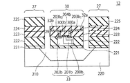
第1の画素部11および第2の画素部12の詳細な構造について図2A乃至図3Bを参照して説明する。図2Aおよび図2Bは、第1実施形態の赤外線撮像素子10の第1の画素部11を図1に示すA−A線およびA’−A’線で切断した断面図であり、図3Aおよび図3Bは、第1実施形態の赤外線撮像素子10の第2の画素部12を図1に示すB−B線およびB’−B’線で切断した断面図である。
Detailed structures of the
第1のセル部20は、支持基板220、絶縁膜221、およびSOI(Silicon on insulator)層からなるSOI基板の支持基板220に設けられた凹部210の上方に、第1の支持脚21a、21bによって支持される(図1、図2A、図2B)。第2の配線部27は凹部210が設けられていない、基板220の領域上に設けられる(図2A、2B)。
The
第1のセル部20は、外部から入射した赤外線を吸収するための第1の赤外線吸収部28と、赤外線吸収によって発生した熱を電気信号に変換する第1の熱電変換部23と、を備える。第1の赤外線吸収部28は、導電層205と、この導電層205を保護するための保護膜224aと、赤外線吸収層223aと、を備える。
The
第1の熱電変換部23は、SOI基板のSOI層に設けられ、pnジャンクションダイオードを構成し、n+領域200aと、p−領域201aと、p+領域202aと、を含む。pnジャンクションはn+領域200aとp−領域201aとの間に形成される。第1の熱電変換部23は、側面が絶縁膜222によって取り囲まれている。p−領域201aはp+領域202aよりも低いp型の不純物濃度を有する。
The first
更に、第1のセル部20は、シリサイドブロック膜204aと、画素内配線22a、22bと、シリサイド膜203a1、203a2と、を備える。シリサイドブロック膜204aは、pnジャンクションにおけるショートを防止する。シリサイド膜203a1およびシリサイド層203a2はそれぞれ、n+領域200aおよびp+領域202aに設けられ、画素内配線22a、22bと第1の熱電変換部23との間を低抵抗で接続する。ここで、導電層205と画素内配線22a、22bとの間の距離および導電層205とシリサイド膜203a2との間の距離をL、導電層205と画素内配線22a若しくは22b若しくはシリサイド膜203a2の間の屈折率をn,検出波長をλとした時に,次式が成り立つことが望ましい。
n・L=λ/4 …(1)
後述する通り,第1のセル部20は導電層205と,画素内配線22a若しくは22b若しくはシリサイド膜203a2の間で干渉による共振を起こさせることによって中赤外線(2μm〜6μm)を吸収するように設計されるから,式(1)により距離Lは0.7〜2.2μmの範囲で設定するのが好ましい。
Further, the
n · L = λ / 4 (1)
As described later, the
なお、画素内配線22aは図1に示すように、対応する第1の配線部26まで延在している。同様に、図1、図2Bに示すように、画素内配線22bは、対応する第2の配線部27まで延在している。
The
第2のセル部30は、第1のセル部20と同様に、SOI基板の支持基板220に設けられた凹部210の上方に、第2の支持脚31a、31bによって支持される(図1、図3A、図3B)。すなわち、第1および第2のセル部20、30の下方の支持基板にはそれぞれ凹部210が設けられ、第1および第2のセル部20、30が凹部210の上方に支持されることによってSOI基板から受ける熱の影響を抑制している。
Similar to the
第2のセル部30は、外部から入射した赤外線を吸収するための第2の赤外線吸収部29と、赤外線吸収によって発生した熱を電気信号に変換する第2の熱電変換部33と、を備える。第2の赤外線吸収部29は、第1の赤外線吸収層224bと、第2の赤外線吸収層223bとを備える。
The
第2の熱電変換部33は、SOI基板のSOI層に設けられ、pn接合ダイオードを構成し、n+領域200bと、p−領域201bと、p+領域202bとを含む。pn接合はn+領域200bとp−領域201bとの間に形成される。第2の熱電変換部33は、側面が絶縁膜222によって取り囲まれている。
The second
更に、第2のセル部30は、シリサイドブロック膜204bと、画素内配線32a、32bと、シリサイド膜203b1、203b2と、を備える。シリサイドブロック膜204bは、pnジャンクションにおけるショートを防止する。シリサイド膜203b1およびシリサイド膜203b2はそれぞれ、n+領域200bおよびp+領域202bに設けられ、画素内配線32a、32bと第2の熱電変換部33との間を低抵抗で接続する。なお、画素内配線32aは図1に示すように、対応する第1の配線部26まで延在している。同様に、図1、図3Bに示すように、画素内配線32bは、対応する第2の配線部27まで延在している。
Further, the
第1のセル部20に対応する第1の配線部26は、図2Bに示すように、絶縁膜222上に設けられた画素内配線22aを覆う赤外線吸収膜223と、この赤外線吸収膜223内に設けられたビア262と、この赤外線吸収膜223上に設けられビア262に接続する配線層264と、この配線層264を覆う赤外線吸収層224と、赤外線吸収層224上に設けられた絶縁膜225と、を備える。配線層264は、バリアメタル層266と、このバリアメタル層266に覆われたメタル配線268と、を備える。なお、第1のセル部20に対応する第2の配線部27は、図2Aに示す断面図には表示されないが、第1の配線部26と同じ構造を有している。
As shown in FIG. 2B, the
第2のセル部30に対応する第1の配線部26は、図3Bに示すように、絶縁膜222上に設けられた画素内配線32aを覆う赤外線吸収膜223と、この赤外線吸収膜223内に設けられたビア262と、赤外線吸収膜223上に設けられビア262に接続する配線層264と、この配線層264を覆う赤外線吸収膜224と、赤外線吸収膜224上に設けられた絶縁膜225と、を備える。配線層264は、バリアメタル層266と、このバリアメタル層266に覆われたメタル配線268と、を備える。なお、第2のセル部30に対応する第2の配線部27は、図3Aに示す断面図には表示されないが、第1の配線部26と同じ構造を有している。
As shown in FIG. 3B, the
(作用)
図4、図5を参照して第1実施形態の赤外線撮像素子の作用について説明する。図4は第1の画素部11における動作を説明する第1のセル部20の断面図である。赤外線撮像素子の外部に設けられた光学系を介して入射した電磁波の内、中赤外線40(波長2μm〜6μm)と、遠赤外線41(7μmより長い波長)の軌跡を示している。
(Function)
The operation of the infrared imaging device of the first embodiment will be described with reference to FIGS. FIG. 4 is a cross-sectional view of the
中赤外線40は酸化膜若しくは窒化膜で構成された保護膜224aを透過して、導電層205に到達する。導電層205は半透過膜として作用し、入射した中赤外線40の一部は導電層205で吸収若しくは反射され、一部は透過して第1のセル部20の深さ方向に進行する。中赤外線40は酸化膜若しくは窒化膜で構成された赤外線吸収層223aも透過し、画素内配線22b若しくはシリサイド膜203a2に到達する。画素内配線22bおよびシリサイド膜203a2は反射膜として作用するため、進行してきた中赤外線40は画素内配線22b若しくはシリサイド膜203a2で反射し、再び赤外線吸収層223aを透過して導電層205に到達する。導電層205に到達した中赤外線40の一部は導電層205で反射する。ここで前術した通り、導電層205と画素内配線22b若しくはシリサイド膜203a2との距離はその光学距離が式(1)を満たすように設計されている。これにより、シリサイド膜203a2で反射して導電層205に向かう中赤外線と,第1のセル部20の外部から入射して導電層205を透過する中赤外線若しくは導電層205で反射して再度シリサイド膜203に向かう中赤外線は互いに共振する。その結果,中赤外線は導電層205とシリサイド膜203a2との間で吸収される。なお,中赤外線が画素内配線22a若しくはシリサイド膜203a1に到達した場合も同様の現象が生じる。
The
一方、第1のセル部20において、遠赤外線41は酸化膜若しくは窒化膜で吸収されるから、入射した遠赤外線41は赤外線吸収層224a若しくは赤外線吸収層223aにて吸収される。従って、第1のセル20においては、中赤外線40、遠赤外線41共に吸収され、セル20の内部において熱エネルギーに変換される。変換された熱エネルギーは熱電変換部23において電気信号に変換され、配線22a、22bを通じてセル20の外部へと伝達される。
On the other hand, since the far
次に、第2の画素部12の作用について図5を参照して説明する。第2の画素部12に入射した電磁波の内、中赤外線40は赤外線吸収層224b、赤外線吸収層223bを透過して画素内配線22b若しくはシリサイド膜203b2に到達する。前記の通り、これらは反射膜として作用するため、進行してきた中赤外線40は画素内配線32b若しくはシリサイド膜203b2で反射する。その後、再び赤外線吸収膜223b、赤外線吸収膜224bを透過して、第2のセル部30の外へと進行する。つまり、第2のセル部30に入射した中赤外線は第2のセル部30の内部で吸収されることがない。なお,中赤外線が画素内配線32a若しくはシリサイド膜203b1に到達した場合も同様である。
Next, the operation of the
一方、遠赤外線41は赤外線吸収膜224b若しくは赤外線吸収膜223bで吸収され、熱エネルギーに変換される。変換された熱エネルギーは熱電変換部33において電気信号に変換され、画素内配線32a、32bを通じて第2のセル部30の外へと伝達される。
On the other hand, the far
以上説明したように、第1の画素部11においては、入射した電磁波の内、中赤外線40および遠赤外線41の双方は、セル22内部で吸収され、最後は電気信号に変換される。これに対して、第2の画素部12においては、入射した電磁波の内、遠赤外線41がセル30の内部で吸収され、最後に電気信号に変換される。つまり、第1の画素部11によって、中赤外線と遠赤外線の吸収による第1の情報(図6に示す実線で表示)が得られ、第2の画素部12によって、遠赤外線の吸収による第2の情報(図6に示す破線で表示)が得られる。これらの情報を加工することで、具体的には第1の情報から第2の情報を減算することで中赤外線の吸収による情報が得られる。したがって、本実施形態によれば、中赤外線による情報と遠赤外線による情報を同時に得ることができるようになる。
As described above, in the
(製造方法)
以下、本実施形態の赤外線撮像素子10の製造方法について図7乃至図17を参照して説明する。図7乃至図17は、本実施形態の赤外線撮像素子10の製造方法を例示する工程断面図である。
(Production method)
Hereinafter, the manufacturing method of the
まず図7に示すように、支持基板220上に絶縁膜221を形成し、絶縁膜221上に半導体層206を形成する。支持基板220には、例えば単結晶シリコン基板が用いられる。絶縁膜221には、例えば、埋め込みシリコン酸化膜が用いられる。半導体層206には、例えば単結晶シリコン層が用いられる。すなわち、SOI基板が形成される。
First, as illustrated in FIG. 7, the insulating
次に図8に示すように、熱電変換部23、33が形成される領域以外の半導体層206を、フォトリソグラフィー技術とエッチング技術とを用いて除去し、半導体層206が除去された領域に素子分離絶縁膜222を埋め込む。エッチングには、例えばRIE(Reactive Ion Etching)を用いることができる。素子分離絶縁膜222には、例えばシリコン酸化膜を用いることができる。この素子分離絶縁膜222は、例えば、半導体層206が除去された空間に、シリコン酸化膜をCVD(Chemical Vapor Deposition)法により埋め込み、CMP(Chemical Mechanical Polishing)で平坦化することによって形成される。この素子分離絶縁膜222に用いられるシリコン酸化膜は、赤外線撮像領域の内部と外部とを分離する素子分離絶縁膜、および複数の画素(赤外線検出素子)どうしを分離する素子分離絶縁膜としても用いられる。続いて、半導体層206の表面部分に、絶縁層207を形成する。この絶縁層207は、半導体層206の表面の部分を酸化させて形成しても良く、また、半導体層206および素子分離絶縁膜222上に別途シリコン酸化膜を設けて形成しても良い。
Next, as shown in FIG. 8, the
次に、図9に示すように、熱電変換部23、33となるpn接合ダイオードを形成する。例えば、半導体層206において、フォトリソグラフィー技術とイオン注入により、p+領域202、p−領域201、およびn+領域200を形成する。具体的には、例えば、フォトリソグラフィー技術により、n+領域200が形成される領域を規定し、イオン注入を行い、n+領域200を形成する。続いて、半導体層206の深い領域に、p+領域202の一部となるp+電極領域2021を形成し、半導体層206の浅い領域(表面)に、p+領域202の別の一部となるp+コンタクト領域2022を形成する。p+コンタクト領域2022は、半導体層206の浅い領域(表面)において、n+領域200と離間している。p+コンタクト領域2022とp+電極領域2021との間に、両者を連結するp+領域202が形成される。p+領域202とn+領域200との間に、p−領域201が形成される。この後、すべての領域において絶縁層207が除去される。
Next, as shown in FIG. 9, pn junction diodes to be the
続いて、半導体層206の表面において、p+領域202のn+領域200側の端部から、n+領域200のp+領域202の側の端部までを覆うように、ブロック膜204を形成する(図9)。ブロック膜204には、例えばシリコン酸化膜を用いることができる。このブロック膜204は、例えば、半導体層206の表面を含む全面にシリコン酸化膜をCVD法によって形成した後、フォトリソグラフィーとRIE法によりこのシリコン酸化膜をパターニングすることによって形成される。また、場合によっては、上記の絶縁層207を除去せず、所定の形状に加工してブロック膜204とすることができる。ブロック膜204は、後述するシリサイド工程において、n+領域200とp−領域201若しくはp+領域202とが電気的に導通しないように、ブロックするための機能を有する。
Subsequently, a
次に、図10に示すように、画素内配線21となる金属膜208を例えばスパッタ法により形成する。金属膜208には、例えばTi膜を用いることができる。金属膜208の厚さは、例えば50nmとすることができる。この後、例えば、650℃の窒素雰囲気中においてアニールすることにより、n+領域200の金属膜208の側の部分にシリサイド膜2031が形成され、p+領域202の金属膜208の側の部分にシリサイド膜2032が形成される。本例では、シリサイド膜2031およびシリサイド膜2032は、TiSi膜である。半導体層206の表面において、n+領域200とp+領域202との間の領域がブロック膜204によって覆われているので、n+領域200とp+領域202との間の領域にはシリサイド膜が形成されず、n+領域200とp−領域201若しくはp+領域202とは電気的に導通しない。なお、金属膜208には、Tiの他に、CoおよびNiなどシリサイドを形成できる任意の金属を用いることができる。
Next, as shown in FIG. 10, a
この製造方法では、第1のセル部20および第2のセル部30における金属膜208の基板220側の層はシリサイド膜、すなわちシリサイド膜2031およびシリサイド膜2032である。これにより、金属膜208と熱電変換部23,33との低抵抗接続が可能となる。
In this manufacturing method, the layers of the
次に、図11に示すように、金属膜208のうち画素内配線として必要な部分以外を除去することで画素内配線22a、22bを形成する。なお、図11は、第1の画素部11を示しているので、第2の画素部12の画素内配線32a、32bは表示されていない。しかし、画素内配線22a、22bの形成と同時に画素内配線32a、32bも形成される。画素内配線の具体的な製造工程は、以下のように行われる。まず、金属膜208のうち画素内配線となる部分をレジスト層(図示せず)で被覆する。続いて、被覆したレジスト層をマスクにして、金属膜208をエッチングして、レジスト層に覆われていない部分の金属膜208を除去する。このエッチングには、例えば、アンモニアと過酸化水素との混合液によるウエットエッチングを用いることができる。この後、上記レジスト層を剥離する。このようにして、画素内配線が形成される。
Next, as shown in FIG. 11,
次に、図12に示すように、CVD法を用いて、赤外線吸収層223aおよび223bとなるシリコン酸化膜223を形成する。
Next, as shown in FIG. 12, a
続いて、図13に示すように第1の画素部11内の第1のセル部20の位置において、導電膜205を例えばスパッタ法により形成する。導電膜205の材料としては、例えばTi,Ni,Co等が好適である。導電膜205の厚さは5nm以下が望ましく、数十nm以下とすることもできる。なお、第2の画素部12の第2のセル部においては、導電膜205は形成しない。
Subsequently, as shown in FIG. 13, a
次に、図14に示すように、導電層205の上から赤外線吸収膜224を形成し、更にその上から絶縁膜225を形成する。かかる状態からフォトリソグラフィー技術とエッチングにより、配線領域以外の絶縁膜225を除去する(図15)。
Next, as shown in FIG. 14, an
次に、第1および第2のセル部20、30と配線領域を分離させるように絶縁膜221、素子分離絶縁膜222、赤外線吸収膜223、赤外線吸収膜224の一部を除去してエッチングホール280を形成する(図16)。エッチングホール280の底面は支持基板220が露出される。この時、平面的には図1に示すように第1支持脚21a、21bおよび第2の支持脚31a、31bが残るように処理がなされる。処理はフォトリソグラフィー技術とエッチングにより行われる。
Next, the insulating
そして、図17に示すように、エッチングホール280を介して、支持基板220の表面部分をエッチングして、第1のセル部20および第2のセル部30と支持基板220との間に凹部210を形成する。このエッチングには、例えばTMAH(Tetra-Methyl-Ammonium-Hydroxide)等の異方性ウエットエッチング材料を用いることができる。以上の工程によって、赤外線撮像素子10が形成される。
Then, as shown in FIG. 17, the surface portion of the
なお、上記製造工程において、図2Bおよび図3Bで示した第1の配線部26の配線層264およびビア262の製造工程は省略している。
In the above manufacturing process, the manufacturing process of the
以上説明したように、本実施形態によれば、光学レンズの切り換えを伴わずに、複数の波長を同時に検出することができる赤外線撮像素子を提供することが可能となる。この赤外線撮像素子は熱電変換により赤外線を検出する方式であるため常温での動作が可能であり、冷却機構が不要となる。このように、本実施形態においては、冷却機構が不要であり、光学レンズの切り換えも伴わないことから、小型化および低コストを実現することができる。 As described above, according to the present embodiment, it is possible to provide an infrared imaging device that can simultaneously detect a plurality of wavelengths without switching optical lenses. Since this infrared imaging device is a system that detects infrared rays by thermoelectric conversion, it can operate at room temperature and does not require a cooling mechanism. As described above, in this embodiment, a cooling mechanism is not necessary and switching of the optical lens is not involved, so that downsizing and low cost can be realized.
(第2実施形態)
次に、図18、図19を参照して第2実施形態による赤外線撮像素子について説明する。図18は、第2実施形態の赤外線撮像素子の中赤外線および遠赤外線を吸収する第1の画素部11を示す断面図であり、図19は、第2実施形態の赤外線撮像素子の遠赤外線を吸収する第2の画素部12を示す断面図である。
(Second Embodiment)
Next, an infrared imaging device according to the second embodiment will be described with reference to FIGS. FIG. 18 is a cross-sectional view illustrating the
図2A、2Bに示す第1実施形態の赤外線撮像素子においては、配線層22a、22bがシリサイド層203a1、203a2の直上に設けたのに対し、図18に示す第2実施形態の第1画素部においては、配線層22a、22bが赤外線吸収層223上に設けられている点および導電層205が設けられない点で異なる。なお、図18、図19においては、図2Bおよび図3Bに示す配線層264およびビア262は省略している。
In the infrared imaging device of the first embodiment shown in FIGS. 2A and 2B, the wiring layers 22a and 22b are provided immediately above the silicide layers 203a 1 and 203a 2 , whereas the first embodiment of the second embodiment shown in FIG. The pixel portion is different in that the wiring layers 22a and 22b are provided on the
この第2実施形態の第1の画素部11においては、pn接合ダイオード上に形成されたシリサイド層203a1と配線層22aとの間はコンタクト層300aによって電気的に接続され、シリサイド層203a2と配線層22bとの間はコンタクト層300bによって電気的に接続されている。
In the
外部から入射した中赤外線は、赤外線吸収層224を透過し、一部が配線層22a、22bによって反射され、残りの中赤外線が配線層22a、22bを透過するとともに、赤外線吸収層223に進行する。そして、シリサイド層203a1、203a2によって反射される。この反射された中赤外線は、赤外線吸収層223を通って配線層22a、22bに達し、配線層22a、22bによって反射される。そうすると、第1実施形態と同様に配線層22a、22bを透過して入射する中赤外線とシリサイド層203a1、203a2によって反射される中赤外線は、シリサイド層203a1と配線層22aとの間およびシリサイド層203a2と配線層22bとの間で共振を起こし、赤外線吸収層223で吸収される。なお、シリサイド層203a1と配線層22aとの間およびシリサイド層203a2と配線層22bとの間の光学距離は、第1実施形態で説明したように、式(1)を満足するように設定される。遠赤外線については赤外線吸収層223若しくは赤外線吸収層224において吸収される。
The mid-infrared light incident from the outside passes through the
一方,図19に示す第2実施形態の第2の画素部12は、基本的な構造は図18に示す第2実施形態の第1の画素部11と同様であるが、第1の画素部11に比べてシリサイドブロック膜204bの幅(図面上で左右方向の長さ)を大きくしかつシリサイド膜203b1、203b2の幅(図面上で左右方向の長さ)がコンタクト300a、300bを形成できる最小幅となるように設定されている。すなわち、シリサイド膜203b1、203b2のサイズがコンタクト300a、300bのサイズと実質的に同一となっている。このように構成すると、シリサイド層203b1、203b2と配線層32a、32bが赤外線吸収層223を介して対向する領域はほとんどなく、中赤外線の共振現象は生じにくくなる。遠赤外線については赤外線吸収層223若しくは224において吸収される。したがって、図19に示す第2の画素部12は、遠赤外線にのみ反応することとなる。
On the other hand, the
このように、第1の画素部11と第2の画素部12において、シリサイド層と配線層とが赤外線吸収層223を介して対向する面積を大きく異ならせることによっても、二波長を分離して捉えることが可能である。
As described above, in the
第2実施形態も第1実施形態と同様に、複数の波長を同時に検出することができる赤外線撮像素子を提供することが可能となる。また、冷却機構が不要であり、光学レンズの切り換えも伴わないことから、小型化および低コストを実現することができる。 Similarly to the first embodiment, the second embodiment can provide an infrared imaging device capable of simultaneously detecting a plurality of wavelengths. In addition, since a cooling mechanism is not required and the optical lens is not switched, downsizing and low cost can be realized.
(変形例)
第2実施形態の変形例による赤外線撮像素子の第1および第2の画素部11、12の断面をそれぞれ図20、21に示す。第1の画素部11における第1の熱電変換部23のn+領域200aおよびp+領域202aの幅(図面上で左右方向の長さ)を、第2の画素部12における第2の熱電変換部33のn+領域200bおよびp+領域202bの幅(図面上で左右方向の長さ)に比べて広くなるように構成されている。
(Modification)
Cross sections of the first and
この変形例のように、熱電変換部23、33のサイズを大きく変えることで、シリサイド層と配線層が赤外線吸収層223を介して対向する面積を第1および第2の画素部で変えることができ、第2実施形態と同様の効果を得ることができる。
As in this modification, the area where the silicide layer and the wiring layer oppose each other via the
(第3実施形態)
次に、第3実施形態による撮像システムについて、図22および図23を参照して説明する。図22は、第3実施形態による撮像システムを示すブロック図である。この実施形態の撮像システムは、第1乃至第2実施形態およびその変形例のいずれかの赤外線撮像素子10および信号処理部350を有する撮像装置400と、この撮像装置400からの信号により被写体の判別を行う判別装置410と、この判別装置410の判別結果に基づいてアラームを発生させるための警報装置420と、を備える。信号処理部350は赤外線撮像素子10から信号を処理して映像信号を生成する。
(Third embodiment)
Next, an imaging system according to the third embodiment will be described with reference to FIGS. FIG. 22 is a block diagram illustrating an imaging system according to the third embodiment. The imaging system according to this embodiment includes an
この実施形態の撮像システムは、例えば,ガソリンの炎検知として使用することができる。ガソリンの炎の相対強度スペクトル、高温物体(例えば1400K)の相対強度スペクトル、および低温物体(例えば350K)の相対強度スペクトルをそれぞれ図23のグラフg1、g2、およびg3に示す。図23からわかるように、ガソリンの炎は中赤外域において、スパイク状のスペクトルを有する。また、ガソリンの炎は中赤外域の強度が遠赤外域の強度に対して非常に高いのに対し、高温物体は中赤外から遠赤外まで幅広く強度が分布している。このため、ガソリンの炎を周知の中赤外線センサで検知することは可能であるが、トータル強度が等しい高温体との区別をすることは困難である。 The imaging system of this embodiment can be used, for example, for gasoline flame detection. Graphs g 1 , g 2 , and g 3 of FIG. 23 show a relative intensity spectrum of a gasoline flame, a relative intensity spectrum of a hot object (eg, 1400 K), and a relative intensity spectrum of a cold object (eg, 350 K), respectively. As can be seen from FIG. 23, the gasoline flame has a spike-like spectrum in the mid-infrared region. Gasoline flames have a very high intensity in the mid-infrared region compared to that in the far-infrared region, whereas high-temperature objects are widely distributed in intensity from the mid-infrared region to the far-infrared region. For this reason, it is possible to detect a gasoline flame with a known mid-infrared sensor, but it is difficult to distinguish it from a high-temperature body having the same total strength.
そこで、本実施形態の撮像装置400の赤外線撮像素子10を用いると、中赤外域の映像と遠赤外域の映像が同時に撮像される。赤外線撮像素子10によって撮像された映像は、信号処理部350において処理され、映像信号が作成される。続いて撮像装置400によって得られた映像信号に基づいて、中赤外映像と遠赤外映像の画素値の比率を判別装置410において計算する。そうすると、中赤外映像の画素値に対する遠赤外映像の画素値の比率によって、被写体の性質を分離することができる。比率と対応する物質のデータを予め判別装置410に保持しておく。そして、撮像された映像がガソリンの炎であると判断された場合には、警報指示信号を警報装置420に送信する。警報装置420では警報指示信号が入力された場合にアラームを発生させ、異常発生をユーザに知らせる。
Therefore, when the
第3実施形態の撮像システムによれば、第1実施形態と同様に、複数の波長を同時に検出することができる。また、冷却機構が不要であり、光学レンズの切り換えも伴わないことから、小型化および低コストを実現することができる。 According to the imaging system of the third embodiment, a plurality of wavelengths can be detected simultaneously as in the first embodiment. In addition, since a cooling mechanism is not required and the optical lens is not switched, downsizing and low cost can be realized.
このように二波長の映像を同時に取得し、それぞれのデータを使用して演算を施すことにより、対象となる物質の検知が可能となる。撮像装置400に用いる光学系は中赤外域から遠赤外域まで透過する材料が望ましく、ゲルマニウムやカルコゲナイドガラスを基材として表面に中赤外域以上の長波長を透過するように設計された反射防止膜を形成したものが好適である。
Thus, by acquiring images of two wavelengths at the same time and performing calculations using the respective data, the target substance can be detected. The optical system used for the
本発明のいくつかの実施形態を説明したが、これらの実施形態は、例として提示したものであり、発明の範囲を限定することは意図していない。これらの実施形態は、その他の様々な形態で実施されることが可能であり、発明の要旨を逸脱しない範囲で、種々の省略、置き換え、変更を行うことができる。これらの実施形態やその変形は、発明の範囲や要旨に含まれると同様に、特許請求の範囲に記載された発明とその均等の範囲に含まれるものである。 Although several embodiments of the present invention have been described, these embodiments are presented by way of example and are not intended to limit the scope of the invention. These embodiments can be implemented in various other forms, and various omissions, replacements, and changes can be made without departing from the scope of the invention. These embodiments and modifications thereof are included in the invention described in the claims and equivalents thereof as well as included in the scope and gist of the invention.
10 赤外線撮像素子
11 第1の画素部
12 第2の画素部
20 第1のセル部
21a、21b 第1の支持脚
22a、22b 画素内配線
23 第1の熱電変換部
26 第1の配線部
27 第2の配線部
28 第1の赤外線吸収部
29 第2の赤外線吸収部
30 第2のセル部
31a、31b 第2の支持脚
32a、32b 画素内配線
33 第2の熱電変換部
200a n+領域
201a p−領域
202a p+領域
200b n+領域
201b p−領域
202b p+領域
203a1、203a2 シリサイド層
203b1、203b2 シリサイド層
204a、204b シリサイドブロック膜
205 導電層
210 凹部
220 支持基板
221 絶縁膜
222 絶縁膜
223、223a、223b 赤外線吸収層
224、224a、224b 赤外線吸収層
225 絶縁層
262 ビア
264 配線層
266 バリアメタル層
268 メタル配線
DESCRIPTION OF
205
Claims (11)
前記第1の凹部の上方に設けられ、外部から入射した第1の赤外線と前記第1の赤外線と波長の異なる第2の赤外線とを検出し、電気信号に変換する第1の赤外線検出部を有する第1のセル部と、前記第1のセル部を前記第1の凹部の上方に支持しかつ前記第1の赤外線検出部によって変換された電気信号を送出する第1および第2の配線を有する第1の支持脚部と、を含む第1の画素部と、
前記第2の凹部の上方に設けられ、前記第2の赤外線を検出し、電気信号に変換する第2の赤外線検出部を有する第2のセル部と、前記第2のセル部を前記第2の凹部の上方に支持しかつ前記第2の赤外線検出部によって変換された電気信号を送出する第3および第4の配線を有する第2の支持脚部と、を含む第2の画素部と、
を備えた赤外線撮像素子。 A substrate provided with first and second recesses on its surface;
A first infrared detector that is provided above the first recess and detects a first infrared ray incident from the outside and a second infrared ray having a wavelength different from that of the first infrared ray, and converts the first infrared ray into an electric signal; A first cell portion having first and second wirings for supporting the first cell portion above the first recess and transmitting an electrical signal converted by the first infrared detection portion; A first pixel portion including: a first support leg having:
A second cell unit provided above the second recess and having a second infrared detector for detecting the second infrared ray and converting it into an electrical signal; and A second pixel portion including a second support leg portion having third and fourth wirings that are supported above the concave portion and that transmit an electrical signal converted by the second infrared detection portion;
Infrared imaging device.
前記第1および第2の赤外線一部を吸収し残りの前記第1および第2の赤外線を透過する第1の赤外線吸収層と、
前記第1の赤外線吸収層の下層に設けられ前記第1および第2の赤外線の一部を吸収し残りの前記第1および第2の赤外線を透過する第2の赤外線吸収層と、
前記第1の赤外線吸収層と前記第2の赤外線吸収層との間に設けられ前記第1の赤外線の一部を透過し残りの前記第1の赤外線を吸収または反射する導電層と、
前記第1および第2の赤外線吸収層ならびに前記導電層によって発生された熱を電気信号に変換する第1の熱電変換部と、
を備え、
前記第2の赤外線検出部は、
前記第1および第2の赤外線の一部を吸収し残りの前記第1および第2の赤外線を透過する第3の赤外線吸収層と、
前記第3の赤外線吸収層の下層に設けられ前記第1および第2の赤外線の一部を吸収し残りの前記第1および第2の赤外線を透過する第4の赤外線吸収層と、
前記第3および第4の赤外線吸収層によって発生された熱を電気信号に変換する第2の熱電変換部と、
を備えている請求項1記載の赤外線撮像素子。 The first infrared detector is
A first infrared absorbing layer that absorbs part of the first and second infrared rays and transmits the remaining first and second infrared rays;
A second infrared absorbing layer provided under the first infrared absorbing layer and absorbing a part of the first and second infrared rays and transmitting the remaining first and second infrared rays;
A conductive layer provided between the first infrared absorbing layer and the second infrared absorbing layer and transmitting a part of the first infrared and absorbing or reflecting the remaining first infrared;
A first thermoelectric converter that converts heat generated by the first and second infrared absorbing layers and the conductive layer into an electrical signal;
With
The second infrared detector is
A third infrared absorbing layer that absorbs part of the first and second infrared rays and transmits the remaining first and second infrared rays;
A fourth infrared absorbing layer provided under the third infrared absorbing layer and absorbing a part of the first and second infrared rays and transmitting the remaining first and second infrared rays;
A second thermoelectric converter that converts heat generated by the third and fourth infrared absorbing layers into an electrical signal;
The infrared imaging device according to claim 1, comprising:
前記第1の熱電変換部において、前記第1および第2のシリサイド層ならびに前記第2半導体領域は前記第2の赤外線吸収層によって覆われかつ前記第1および第2のシリサイド層のそれぞれと前記導電層との間の光学距離は前記第1の赤外線の波長の1/4であり、前記第1および第2のシリサイド層はそれぞれ前記第1および第2の画素内配線に接続され、
前記第2の熱電変換部において、前記第1および第2のシリサイド層ならびに前記第2半導体領域は前記第4の赤外線吸収層によって覆われ、前記第1および第2のシリサイド層はそれぞれ前記第1および第2の配線に接続され、前記第1および第2のシリサイド層はそれぞれ前記第3および第4の配線に接続される請求項2記載の赤外線撮像素子。 The first and second thermoelectric conversion units are provided on a p-type first semiconductor region and a partial region of the first semiconductor region, respectively, and have a lower p-type impurity concentration than the first semiconductor region. a p-type second semiconductor region, an n-type third semiconductor region provided on a partial region of the second semiconductor region, and the first semiconductor region and the third semiconductor region, respectively. First and second silicide layers,
In the first thermoelectric conversion section, the first and second silicide layers and the second semiconductor region are covered with the second infrared absorption layer and are electrically connected to the first and second silicide layers, respectively. The optical distance between the layers is ¼ of the wavelength of the first infrared ray, and the first and second silicide layers are connected to the first and second intra-pixel wirings, respectively.
In the second thermoelectric conversion section, the first and second silicide layers and the second semiconductor region are covered with the fourth infrared absorption layer, and the first and second silicide layers are respectively the first and second silicide layers. The infrared imaging element according to claim 2, wherein the first and second silicide layers are connected to the third and fourth wirings, respectively.
前記第1および第2の赤外線の一部を吸収し残りの前記第1および第2の赤外線を透過する第1の赤外線吸収層と、
前記第1の赤外線吸収層の下層に設けられ前記第1および第2の赤外線の一部を吸収し残りの前記第1および第2の赤外線を透過する第2の赤外線吸収層と、
p型の第1半導体領域と、前記第1半導体領域の一部の領域上に設けられ前記第1半導体領域よりもp型の不純物濃度の低いp型の第2半導体領域と、前記第2半導体領域の一部の領域上に設けられたn型の第3半導体領域と、前記第1半導体領域および前記第3半導体領域上にそれぞれ設けられた第1および第2のシリサイド層と、を有し、前記第1および第2の赤外線吸収層によって発生された熱を電気信号に変換する第1の熱電変換部と、
前記第2の赤外線吸収層上に設けられ前記第1および第2の配線とそれぞれ接続する第1および第2の画素内配線と、
前記第2の赤外線吸収層に設けられ前記第1の画素内配線と前記第1のシリサイド層と接続する第1のコンタクトと、
前記第2の赤外線吸収層に設けられ前記第2の画素内配線と前記第2のシリサイド層と接続する第2のコンタクトと、
を備え、
前記第2の赤外線検出部は、
前記第1および第2の赤外線の一部を吸収し残りの前記第1および第2の赤外線を透過する第3の赤外線吸収層と、
前記第3の赤外線吸収層の下層に設けられ前記第1および第2の赤外線の一部を吸収し残りの前記第1および第2の赤外線を透過する第4の赤外線吸収層と、
p型の第4半導体領域と、前記第4半導体領域の一部の領域上に設けられ前記第4半導体領域よりもp型の不純物濃度の低いp型の第5半導体領域と、前記第5半導体領域の一部の領域上に設けられたn型の第6半導体領域と、前記第4半導体領域および前記第6半導体領域上にそれぞれ設けられた第3および第4のシリサイド層と、を有し、前記第3および第4の赤外線吸収層によって発生された熱を電気信号に変換する第2の熱電変換部と、
前記第4の赤外線吸収層上に設けられ前記第3および第4配線にそれぞれ接続する第3および第4の画素内配線と、
前記第3の画素内配線と前記第3のシリサイド層と接続する第3のコンタクトと、
前記第4の画素内配線と前記第4のシリサイド層と接続する第4のコンタクトと、
を備え、
前記第3および第4のシリサイド層の幅はそれぞれ、前記第1および第2のシリサイド層の幅よりも狭く、第3および第4のコンタクトと実質的に同じサイズである請求項1記載の赤外線撮像素子。 The first infrared detector is
A first infrared absorbing layer that absorbs part of the first and second infrared rays and transmits the remaining first and second infrared rays;
A second infrared absorbing layer provided under the first infrared absorbing layer and absorbing a part of the first and second infrared rays and transmitting the remaining first and second infrared rays;
a p-type first semiconductor region; a p-type second semiconductor region provided on a partial region of the first semiconductor region; and having a p-type impurity concentration lower than that of the first semiconductor region; and the second semiconductor An n-type third semiconductor region provided on a partial region of the region, and first and second silicide layers provided on the first semiconductor region and the third semiconductor region, respectively. A first thermoelectric converter that converts heat generated by the first and second infrared absorbing layers into an electrical signal;
First and second intra-pixel wirings provided on the second infrared absorption layer and connected to the first and second wirings, respectively;
A first contact provided in the second infrared absorption layer and connected to the first intra-pixel wiring and the first silicide layer;
A second contact provided in the second infrared absorption layer and connected to the second intra-pixel wiring and the second silicide layer;
With
The second infrared detector is
A third infrared absorbing layer that absorbs part of the first and second infrared rays and transmits the remaining first and second infrared rays;
A fourth infrared absorbing layer provided under the third infrared absorbing layer and absorbing a part of the first and second infrared rays and transmitting the remaining first and second infrared rays;
a p-type fourth semiconductor region, a p-type fifth semiconductor region provided on a partial region of the fourth semiconductor region and having a p-type impurity concentration lower than that of the fourth semiconductor region, and the fifth semiconductor An n-type sixth semiconductor region provided on a partial region of the region, and third and fourth silicide layers provided on the fourth semiconductor region and the sixth semiconductor region, respectively. A second thermoelectric converter that converts heat generated by the third and fourth infrared absorbing layers into an electrical signal;
Third and fourth intra-pixel wirings provided on the fourth infrared absorbing layer and connected to the third and fourth wirings, respectively.
A third contact connecting the third intra-pixel wiring and the third silicide layer;
A fourth contact connecting the fourth intra-pixel wiring and the fourth silicide layer;
With
2. The infrared ray according to claim 1, wherein the widths of the third and fourth silicide layers are smaller than the widths of the first and second silicide layers, respectively, and are substantially the same size as the third and fourth contacts. Image sensor.
前記第1および第2の赤外線の一部を吸収し残りの前記第1および第2の赤外線を透過する第1の赤外線吸収層と、
前記第1の赤外線吸収層の下層に設けられ前記第1および第2の赤外線の一部を吸収し残りの前記第1および第2の赤外線を透過する第2の赤外線吸収層と、
p型の第1半導体領域と、前記第1半導体領域の一部の領域上に設けられ前記第1半導体領域よりもp型の不純物濃度の低いp型の第2半導体領域と、前記第2半導体領域の一部の領域上に設けられたn型の第3半導体領域と、前記第1半導体領域および前記第3半導体領域上にそれぞれ設けられた第1およぶ第2のシリサイド層と、を有し、前記第1および第2の赤外線吸収層によって発生された熱を電気信号に変換する第1の熱電変換部と、
前記第2の赤外線吸収層上に設けられ前記第1および第2配線にそれぞれ接続する第1および第2の画素内配線と、
前記第1の画素内配線と前記第1のシリサイド層と接続する第1のコンタクトと、
前記第2の画素内配線と前記第2のシリサイド層と接続する第2のコンタクトと、
を備え、
前記第2の赤外線検出部は、
前記第1および第2の赤外線の一部を吸収し残りの前記第1および第2の赤外線を透過する第3の赤外線吸収層と、
前記第3の赤外線吸収層の下層に設けられ前記第1および第2の赤外線の一部を吸収し残りの前記第1および第2の赤外線を透過する第4の赤外線吸収層と、
p型の第4半導体領域と、前記第4半導体領域の一部の領域上に設けられ前記第4半導体領域よりもp型の不純物濃度の低いp型の第5半導体領域と、前記第5半導体領域の一部の領域上に設けられたn型の第6半導体領域と、前記第4半導体領域および前記第6半導体領域上にそれぞれ設けられた第3およぶ第4のシリサイド層と、を有し、前記第3および第4の赤外線吸収層によって発生された熱を電気信号に変換する第2の熱電変換部と、
前記第4の赤外線吸収層上に設けられ前記第3および第4配線にそれぞれ接続する第3および第4の画素内配線と、
前記第3の画素内配線と前記第3のシリサイド層と接続する第3のコンタクトと、
前記第4の画素内配線と前記第4のシリサイド層と接続する第4のコンタクトと、
を備え、
前記第2の熱電変換部の幅は、前記第1の熱電変換部の幅よりも狭く、
前記第3および第4のシリサイド層の幅はそれぞれ、前記第1および第2のシリサイド層の幅よりも狭い請求項1記載の赤外線撮像素子。 The first infrared detector is
A first infrared absorbing layer that absorbs part of the first and second infrared rays and transmits the remaining first and second infrared rays;
A second infrared absorbing layer provided under the first infrared absorbing layer and absorbing a part of the first and second infrared rays and transmitting the remaining first and second infrared rays;
a p-type first semiconductor region; a p-type second semiconductor region provided on a partial region of the first semiconductor region; and having a p-type impurity concentration lower than that of the first semiconductor region; and the second semiconductor An n-type third semiconductor region provided on a partial region of the region, and first and second silicide layers provided on the first semiconductor region and the third semiconductor region, respectively. A first thermoelectric converter that converts heat generated by the first and second infrared absorbing layers into an electrical signal;
First and second intra-pixel wirings provided on the second infrared absorption layer and connected to the first and second wirings, respectively.
A first contact connecting the first intra-pixel wiring and the first silicide layer;
A second contact connecting the second intra-pixel wiring and the second silicide layer;
With
The second infrared detector is
A third infrared absorbing layer that absorbs part of the first and second infrared rays and transmits the remaining first and second infrared rays;
A fourth infrared absorbing layer provided under the third infrared absorbing layer and absorbing a part of the first and second infrared rays and transmitting the remaining first and second infrared rays;
a p-type fourth semiconductor region, a p-type fifth semiconductor region provided on a partial region of the fourth semiconductor region and having a p-type impurity concentration lower than that of the fourth semiconductor region, and the fifth semiconductor An n-type sixth semiconductor region provided on a partial region of the region, and third and fourth silicide layers provided on the fourth semiconductor region and the sixth semiconductor region, respectively. A second thermoelectric converter that converts heat generated by the third and fourth infrared absorbing layers into an electrical signal;
Third and fourth intra-pixel wirings provided on the fourth infrared absorbing layer and connected to the third and fourth wirings, respectively.
A third contact connecting the third intra-pixel wiring and the third silicide layer;
A fourth contact connecting the fourth intra-pixel wiring and the fourth silicide layer;
With
The width of the second thermoelectric conversion unit is narrower than the width of the first thermoelectric conversion unit,
2. The infrared imaging device according to claim 1, wherein the third and fourth silicide layers are narrower than the first and second silicide layers, respectively.
各列に対応して隣接する列間の前記基板上に設けられ、対応する列における前記第1の画素部の前記第2の配線および前記第2の画素部の前記第4の配線が接続される第2の配線部と、
を備えている請求項7記載の赤外線撮像素子。 A first wiring provided on the substrate between adjacent rows corresponding to each row, to which the first wiring of the first pixel portion and the third wiring of the second pixel portion in the corresponding row are connected. 1 wiring part;
Provided on the substrate between adjacent columns corresponding to each column, and the second wiring of the first pixel portion and the fourth wiring of the second pixel portion in the corresponding column are connected. A second wiring portion,
An infrared imaging device according to claim 7.
前記赤外線撮像素子によって撮像されて信号を処理する信号処理部と、
を備えた撮像装置。 An infrared imaging device according to any one of claims 1 to 9,
A signal processing unit that processes an image captured by the infrared imaging device;
An imaging apparatus comprising:
前記撮像装置の前記信号処理部よって処理された信号に基づいて、被写体の判別を行う判別装置と、
前記判別装置によって判別結果に応じて警報を発生する警報装置と、
を備えている撮像システム。 An imaging device according to claim 10;
A discriminating device for discriminating a subject based on a signal processed by the signal processing unit of the imaging device;
An alarm device for generating an alarm according to a determination result by the determination device;
An imaging system comprising:
Priority Applications (4)
| Application Number | Priority Date | Filing Date | Title |
|---|---|---|---|
| JP2013237277A JP2015096842A (en) | 2013-11-15 | 2013-11-15 | Infrared imaging element, imaging device, and imaging system |
| KR1020140134201A KR20150056453A (en) | 2013-11-15 | 2014-10-06 | Infrared imaging element, imaging device, and imaging system |
| US14/534,628 US20150136984A1 (en) | 2013-11-15 | 2014-11-06 | Infrared imaging element, imaging device, and imaging system |
| EP14192439.9A EP2873955A3 (en) | 2013-11-15 | 2014-11-10 | Infrared imaging element, imaging device, and imaging system |
Applications Claiming Priority (1)
| Application Number | Priority Date | Filing Date | Title |
|---|---|---|---|
| JP2013237277A JP2015096842A (en) | 2013-11-15 | 2013-11-15 | Infrared imaging element, imaging device, and imaging system |
Publications (1)
| Publication Number | Publication Date |
|---|---|
| JP2015096842A true JP2015096842A (en) | 2015-05-21 |
Family
ID=51900723
Family Applications (1)
| Application Number | Title | Priority Date | Filing Date |
|---|---|---|---|
| JP2013237277A Pending JP2015096842A (en) | 2013-11-15 | 2013-11-15 | Infrared imaging element, imaging device, and imaging system |
Country Status (4)
| Country | Link |
|---|---|
| US (1) | US20150136984A1 (en) |
| EP (1) | EP2873955A3 (en) |
| JP (1) | JP2015096842A (en) |
| KR (1) | KR20150056453A (en) |
Families Citing this family (3)
| Publication number | Priority date | Publication date | Assignee | Title |
|---|---|---|---|---|
| US10439118B2 (en) * | 2014-12-04 | 2019-10-08 | Maxim Integrated Products, Inc. | MEMS-based wafer level packaging for thermo-electric IR detectors |
| CN108351254B (en) * | 2016-09-02 | 2021-10-22 | 索尼半导体解决方案公司 | camera |
| CN116724217A (en) * | 2021-01-25 | 2023-09-08 | 索尼集团公司 | Thermal detection elements and image sensors |
Family Cites Families (8)
| Publication number | Priority date | Publication date | Assignee | Title |
|---|---|---|---|---|
| US5811815A (en) * | 1995-11-15 | 1998-09-22 | Lockheed-Martin Ir Imaging Systems, Inc. | Dual-band multi-level microbridge detector |
| JP3597069B2 (en) * | 1999-01-12 | 2004-12-02 | 日本電気株式会社 | Thermal infrared array sensor for detecting multiple infrared wavelength bands |
| JP3675770B2 (en) * | 2002-03-22 | 2005-07-27 | 株式会社東芝 | Thermal infrared image sensor |
| US7491938B2 (en) * | 2004-03-23 | 2009-02-17 | Bae Systems Information And Electronic Systems Integration Inc. | Multi-spectral uncooled microbolometer detectors |
| US7838869B2 (en) * | 2005-10-21 | 2010-11-23 | Georgia State University Research Foundation, Inc. | Dual band photodetector |
| JP4975669B2 (en) * | 2008-03-25 | 2012-07-11 | 株式会社東芝 | Infrared detector and solid-state imaging device equipped with the infrared detector |
| US20140042324A1 (en) * | 2012-08-08 | 2014-02-13 | Agency For Science, Technology And Research | Detector and method of controlling the same |
| US9261411B2 (en) * | 2012-12-19 | 2016-02-16 | Institut National D'optique | Uncooled microbolometer detector and array for terahertz detection |
-
2013
- 2013-11-15 JP JP2013237277A patent/JP2015096842A/en active Pending
-
2014
- 2014-10-06 KR KR1020140134201A patent/KR20150056453A/en not_active Ceased
- 2014-11-06 US US14/534,628 patent/US20150136984A1/en not_active Abandoned
- 2014-11-10 EP EP14192439.9A patent/EP2873955A3/en not_active Withdrawn
Also Published As
| Publication number | Publication date |
|---|---|
| KR20150056453A (en) | 2015-05-26 |
| EP2873955A3 (en) | 2015-11-04 |
| US20150136984A1 (en) | 2015-05-21 |
| EP2873955A2 (en) | 2015-05-20 |
Similar Documents
| Publication | Publication Date | Title |
|---|---|---|
| JP6291760B2 (en) | Thermocouple, thermopile, infrared sensor, and method for manufacturing infrared sensor | |
| JP6903396B2 (en) | Image sensor and image sensor | |
| JP6889981B2 (en) | Surface microfabrication infrared sensor using high temperature stability interference type absorber | |
| US9130082B2 (en) | Apparatus for generating/detecting terahertz wave using graphene and manufacturing method of the same | |
| JP6668036B2 (en) | Imaging device and method for manufacturing the same, and imaging device and method for manufacturing the same | |
| EP2384425B1 (en) | Teramos-terahertz thermal sensor and focal plane array | |
| US6573504B2 (en) | Infrared sensor and manufacturing method thereof | |
| JP5801151B2 (en) | Infrared detector based on suspended bolometer microplate | |
| US20120061569A1 (en) | Thermal infrared sensor and manufacturing method thereof | |
| US20110006193A1 (en) | Anti-resonant reflecting optical waveguide for imager light pipe | |
| JP2009229401A (en) | Infrared radiation detector and solid state imaging element equipped with infrared radiation detector | |
| US20250120206A1 (en) | Photodetector, photodetector manufacturing method, and electronic equipment | |
| JP2020013842A (en) | Photoelectric conversion element and light receiving device | |
| JP3675770B2 (en) | Thermal infrared image sensor | |
| JP2009174917A (en) | Infrared detecting element and method for manufacturing infrared detecting element | |
| JP2015096842A (en) | Infrared imaging element, imaging device, and imaging system | |
| JP6440805B1 (en) | Thermal infrared detector and method for manufacturing the same | |
| US8304848B2 (en) | Infrared imaging device and method of manufacturing the same | |
| CN109560093B (en) | Semiconductor image sensor having a plurality of pixels | |
| JP2006300623A (en) | Infrared sensor | |
| JP5884568B2 (en) | Manufacturing method of thermal infrared sensor | |
| JP2006177712A (en) | Semiconductor device and manufacturing method thereof | |
| JP2015169533A (en) | Thermal infrared sensor and method for manufacturing the same | |
| US20140235009A1 (en) | Method for making an imager device | |
| JP2008082790A (en) | Infrared sensor |