JP2014202645A - Measuring instrument - Google Patents
Measuring instrument Download PDFInfo
- Publication number
- JP2014202645A JP2014202645A JP2013079924A JP2013079924A JP2014202645A JP 2014202645 A JP2014202645 A JP 2014202645A JP 2013079924 A JP2013079924 A JP 2013079924A JP 2013079924 A JP2013079924 A JP 2013079924A JP 2014202645 A JP2014202645 A JP 2014202645A
- Authority
- JP
- Japan
- Prior art keywords
- light
- test
- phase
- test light
- interference signal
- Prior art date
- Legal status (The legal status is an assumption and is not a legal conclusion. Google has not performed a legal analysis and makes no representation as to the accuracy of the status listed.)
- Pending
Links
Images


Classifications
-
- G—PHYSICS
- G01—MEASURING; TESTING
- G01B—MEASURING LENGTH, THICKNESS OR SIMILAR LINEAR DIMENSIONS; MEASURING ANGLES; MEASURING AREAS; MEASURING IRREGULARITIES OF SURFACES OR CONTOURS
- G01B9/00—Measuring instruments characterised by the use of optical techniques
- G01B9/02—Interferometers
- G01B9/02015—Interferometers characterised by the beam path configuration
-
- G—PHYSICS
- G01—MEASURING; TESTING
- G01B—MEASURING LENGTH, THICKNESS OR SIMILAR LINEAR DIMENSIONS; MEASURING ANGLES; MEASURING AREAS; MEASURING IRREGULARITIES OF SURFACES OR CONTOURS
- G01B9/00—Measuring instruments characterised by the use of optical techniques
- G01B9/02—Interferometers
- G01B9/02041—Interferometers characterised by particular imaging or detection techniques
- G01B9/02042—Confocal imaging
-
- G—PHYSICS
- G01—MEASURING; TESTING
- G01B—MEASURING LENGTH, THICKNESS OR SIMILAR LINEAR DIMENSIONS; MEASURING ANGLES; MEASURING AREAS; MEASURING IRREGULARITIES OF SURFACES OR CONTOURS
- G01B9/00—Measuring instruments characterised by the use of optical techniques
- G01B9/02—Interferometers
- G01B9/02041—Interferometers characterised by particular imaging or detection techniques
- G01B9/02044—Imaging in the frequency domain, e.g. by using a spectrometer
Landscapes
- Physics & Mathematics (AREA)
- General Physics & Mathematics (AREA)
- Instruments For Measurement Of Length By Optical Means (AREA)
Abstract
【課題】参照光と被検光との光路長差に対応する距離を高精度に計測するのに有利な技術を提供する。【解決手段】光源101から射出された光から分割される第1被検光が通過する第1光学系、及び、第2被検光が通過する第2光学系と、被検面100で反射された第1被検光及び第2被検光のそれぞれと参照面104で反射された参照光との干渉光を検出する検出部113と、検出部113で検出された干渉光に基づいて、距離を求める処理部115と、を有し、第1光学系における光学的パワーと第2光学系における光学的パワーとが異なり、第1被検光及び第2被検光の被検面側の集光点P01,P02,P11,P12と被検面との間の距離は、複数の波長のそれぞれに応じて互いに異なり、集光点と被検面との間の距離が所定距離となる集光点に対応する波長の第1被検光及び第2被検光のそれぞれを検出部113に導く導光部を更に有することを特徴とする。【選択図】図1A technique advantageous in measuring a distance corresponding to an optical path length difference between reference light and test light with high accuracy is provided. A first optical system through which a first test light split from light emitted from a light source passes, a second optical system through which a second test light passes, and a test surface that reflects the light. Based on the interference light detected by the detection unit 113 and the detection unit 113 that detects the interference light between each of the first test light and the second test light that has been performed and the reference light reflected by the reference surface 104, A processing unit 115 for obtaining a distance, the optical power in the first optical system is different from the optical power in the second optical system, and the first test light and the second test light are on the test surface side. The distances between the condensing points P01, P02, P11, and P12 and the test surface are different from each other according to each of a plurality of wavelengths, and the distance between the condensing points and the test surface is a predetermined distance. A light guide that guides each of the first test light and the second test light having a wavelength corresponding to the light spot to the detection unit 113; Characterized in that it has a. [Selection] Figure 1
Description
本発明は、被検光と参照光との光路長差に対応する距離を計測する計測装置に関する。 The present invention relates to a measuring apparatus that measures a distance corresponding to an optical path length difference between test light and reference light.
被検光と参照光との光路長差に対応する距離を計測する計測装置として、分光干渉計や波長走査干渉計が知られている。分光干渉計は、複数の波長を含む光を射出する光源を用いて、被検光と参照光との干渉光を分光して検出し、干渉光の強度や位相などの情報を含む干渉信号(波長ごとの干渉信号)に基づいて、被検光と参照光との光路長差に対応する距離を求めている。また、波長走査干渉計は、波長を走査(変更)することが可能な光源を用いて、被検光と参照光との干渉光の強度や位相を検出し、波長を走査することで得られる波長ごとの干渉信号に基づいて、被検光と参照光との光路長差に対応する距離を求めている。 A spectroscopic interferometer and a wavelength scanning interferometer are known as a measuring device for measuring a distance corresponding to the optical path length difference between the test light and the reference light. The spectroscopic interferometer uses a light source that emits light including a plurality of wavelengths to detect and detect interference light between the test light and the reference light, and includes an interference signal including information such as the intensity and phase of the interference light ( Based on the interference signal for each wavelength, the distance corresponding to the optical path length difference between the test light and the reference light is obtained. The wavelength scanning interferometer is obtained by scanning the wavelength by detecting the intensity and phase of the interference light between the test light and the reference light using a light source capable of scanning (changing) the wavelength. The distance corresponding to the optical path length difference between the test light and the reference light is obtained based on the interference signal for each wavelength.
分光干渉計や波長走査干渉計などの計測装置において、被検面に対する横方向分解能(計測する距離方向と垂直な面方向の分解能)や計測精度を向上させるためには、被検面を照射する光の照射スポット径を小さくすればよい。照射スポット径を小さくするには、被検面に光を照射する照射光学系の開口数(NA)を増加すればよいが、開口数を増加すると焦点深度が減少するため、被検光と参照光との光路長差に対応する距離の計測可能レンジが減少してしまう。このように、計測精度(照射スポット径)と計測可能レンジとは相反関係にあり、両立することが困難である。 In measuring devices such as a spectroscopic interferometer and a wavelength scanning interferometer, in order to improve the lateral resolution (resolution in the direction perpendicular to the distance direction to be measured) and measurement accuracy with respect to the test surface, the test surface is irradiated. What is necessary is just to make the irradiation spot diameter of light small. In order to reduce the irradiation spot diameter, the numerical aperture (NA) of the irradiation optical system that irradiates light to the surface to be measured can be increased. However, increasing the numerical aperture decreases the depth of focus. The measurable range of the distance corresponding to the optical path length difference with light decreases. Thus, the measurement accuracy (irradiation spot diameter) and the measurable range are in a contradictory relationship, and it is difficult to achieve both.
そこで、高い計測精度と広い計測可能レンジとを両立することが可能な技術として、波長共焦点(Chromatic Confocal)の構成を有する分光干渉計が提案されている(非特許文献1参照)。ここで、波長共焦点の構成とは、軸上色収差を発生させる光学系と、共焦点用のフィルターとを含む構成である。また、波長走査干渉計において、互いに離散した波長帯域における干渉信号を取得し、それらの干渉信号に基づいて被検光と参照光との光路長差に対応する距離を算出することで、計測精度を向上させる技術も提案されている(特許文献1及び非特許文献2参照)。
Therefore, a spectral interferometer having a wavelength confocal configuration has been proposed as a technique capable of achieving both high measurement accuracy and a wide measurable range (see Non-Patent Document 1). Here, the wavelength confocal configuration is a configuration including an optical system that generates axial chromatic aberration and a confocal filter. In addition, the wavelength scanning interferometer acquires interference signals in discrete wavelength bands, and calculates the distance corresponding to the optical path length difference between the test light and the reference light based on the interference signals, thereby measuring accuracy. The technique which improves this is also proposed (refer
しかしながら、非特許文献1に開示された技術では、波長共焦点の原理によって、被検面の近傍に集光点(像点)を有する限定的な波長帯域における干渉信号しか検出することができない。従って、高精度な距離計測を行うために必要となる広い波長帯域における干渉信号を確保することが困難であるため、計測誤差が増加し、被検光と参照光との光路長差に対応する距離を高精度で計測することができない。
However, the technique disclosed in
また、従来から、計測に使用する波長帯域を十分に確保できずに計測精度が低下するという課題に対して、例えば、特許文献1や非特許文献2などのように、互いに離散した波長帯域における干渉信号に基づいて距離を算出する技術が知られている。但し、これらの技術を、非特許文献1に開示された技術にそのまま適用することはできない。これは、波長共焦点の原理によって、検出可能な波長帯域が被検面の近傍に集光点を有する波長帯域に限定されるため、その波長帯域から離散した波長帯域は共焦点用のフィルターで遮断され、離散した波長帯域における干渉信号を得ることができないからである。
Further, conventionally, with respect to the problem that the measurement accuracy is lowered without sufficiently securing the wavelength band used for measurement, for example, in the wavelength bands discrete from each other as in
本発明は、このような従来技術の課題に鑑みてなされ、被検光と参照光との光路長差に対応する距離を高精度に計測するのに有利な技術を提供することを例示的目的とする。 The present invention has been made in view of such a problem of the prior art, and an exemplary object thereof is to provide a technique advantageous for measuring a distance corresponding to the optical path length difference between the test light and the reference light with high accuracy. And
上記目的を達成するために、本発明の一側面としての計測装置は、被検光と参照光との光路長差に対応する距離を計測する計測装置であって、光源から射出された光から分割される第1被検光及び第2被検光のうち、前記第1被検光が通過する第1光学系、及び、前記第2被検光が通過する第2光学系と、前記被検面で反射された前記第1被検光及び前記第2被検光のそれぞれと前記参照面で反射された参照光との干渉光を検出する検出部と、前記検出部で検出された干渉光に基づいて、前記距離を求める処理部と、を有し、前記第1光学系における光学的パワーと前記第2光学系における光学的パワーとが異なり、前記第1被検光の前記被検面側の集光点と前記被検面との間の距離は、複数の波長のそれぞれに応じて互いに異なり、前記第2被検光の前記被検面側の集光点と前記被検面との間の距離は、複数の波長のそれぞれに応じて互いに異なり、前記集光点と前記被検面との間の距離が所定距離となる集光点に対応する波長の前記第1被検光及び前記第2被検光のそれぞれを前記検出部に導く導光部を更に有することを特徴とする。 In order to achieve the above object, a measuring device according to one aspect of the present invention is a measuring device that measures a distance corresponding to a difference in optical path length between test light and reference light, and includes a light source that emits light from a light source. Of the first and second test lights to be divided, the first optical system through which the first test light passes, the second optical system through which the second test light passes, and the test light A detection unit that detects interference light between each of the first test light and the second test light reflected by the inspection surface and the reference light reflected by the reference surface, and interference detected by the detection unit A processing unit for obtaining the distance based on light, wherein the optical power in the first optical system is different from the optical power in the second optical system, and the test of the first test light is performed. The distance between the condensing point on the surface side and the test surface is different from each other according to each of a plurality of wavelengths. The distance between the condensing point on the test surface side of the test light and the test surface is different from each other according to each of a plurality of wavelengths, and the distance between the condensing point and the test surface Is further characterized by further comprising a light guide section that guides each of the first test light and the second test light having a wavelength corresponding to a condensing point having a predetermined distance to the detection section.
本発明の更なる目的又はその他の側面は、以下、添付図面を参照して説明される好ましい実施形態によって明らかにされるであろう。 Further objects and other aspects of the present invention will become apparent from the preferred embodiments described below with reference to the accompanying drawings.
本発明によれば、例えば、被検光と参照光との光路長差に対応する距離を高精度に計測するのに有利な技術を提供することができる。 ADVANTAGE OF THE INVENTION According to this invention, the technique advantageous for measuring the distance corresponding to the optical path length difference of test light and reference light with high precision can be provided, for example.
以下、添付図面を参照して、本発明の好適な実施の形態について説明する。なお、各図において、同一の部材については同一の参照番号を付し、重複する説明は省略する。 DESCRIPTION OF EXEMPLARY EMBODIMENTS Hereinafter, preferred embodiments of the invention will be described with reference to the accompanying drawings. In addition, in each figure, the same reference number is attached | subjected about the same member and the overlapping description is abbreviate | omitted.
<第1の実施形態>
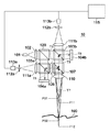
図1は、本発明の第1の実施形態における計測装置10の構成を示す概略図である。計測装置10は、被検光と参照光との光路長差に対応する距離を計測する計測装置であって、例えば、分光干渉計の構成を有する。計測装置10は、複数の波長を含む光を射出する光源101と、光学素子102と、分割素子103と、参照面104と、分割素子105と、光学素子106と、分割素子107と、反射素子108及び109と、光学素子110とを有する。また、計測装置10は、光学素子111と、波長選択部112と、検出部113と、処理部115とを有する。
<First Embodiment>
FIG. 1 is a schematic diagram illustrating a configuration of a
計測装置10は、光源101から射出した光を、所定の軸上色収差を有する光学素子110を介して、被検面100に照射する。また、計測装置10は、被検面100で反射された光と参照面104で反射された光との干渉光を検出部113で検出し、かかる干渉光から得られる干渉信号に基づいて、被検光と参照光との光路長差に対応する距離を処理部115で算出する。
The
計測装置10の構成の詳細について、光源101から射出する光の経路に沿って説明する。光源101からの光は、光学素子102によってコリメートされ、分割素子103に入射する。分割素子103は、光源101からの光を、分割素子105に向かう被検光と、参照面104に向かう参照光とに分割する。また、被検光は、分割素子105によって、光学素子106に向かう第1被検光と、反射素子108に向かう第2被検光とに分割される。
Details of the configuration of the
以下では、説明を簡単にするために、分割素子105、光学素子106、分割素子107、光学素子110及び被検面100を順に、或いは、逆に通過する経路を第1経路と称する。同様に、分割素子105、反射素子108、反射素子109、分割素子107、光学素子110及び被検面100を順に、或いは、逆に通過する経路を第2経路と称する。
Hereinafter, in order to simplify the description, a path that passes through the splitting
後述するように、計測装置10においては、第1被検光に対応する第1光学系における光学的パワーと第2被検光に対応する第2光学系における光学的パワーとが異なる。また、第1光学系及び第2光学系は、第1被検光の経路の一部と第2被検光の経路の一部とが共通する共通部分を含む。
As will be described later, in the
第1被検光は、第1経路において、光学的パワーを有する光学素子(例えば、レンズ)106によって屈折力を付加され、光学的パワー有する光学素子(例えば、レンズ)110によって軸上色収差を付加される。これにより、第1被検光は、被検面100に対して、複数の波長のそれぞれで(即ち、波長ごとに)互いに異なる位置に集光点(像点)を形成する。被検面100で反射した第1被検光は、第1経路を通過し、分割素子103及び光学素子111を順に経て、波長選択部112に入射する。
In the first path, the first test light is given a refractive power by an optical element (for example, a lens) 106 having optical power and an axial chromatic aberration is added by an optical element (for example, lens) 110 having optical power. Is done. As a result, the first test light forms a condensing point (image point) at different positions with respect to the
第2被検光は、第2経路を通過し、光学素子110によって軸上色収差を付加され、被検面100に対して、複数の波長のそれぞれで(即ち、波長ごとに)互いに異なる位置に集光点(像点)を形成する。被検面100で反射した第2被検光は、第2経路を通過し、分割素子103及び光学素子111を順に経て、波長選択部112に入射する。
The second test light passes through the second path, is subjected to axial chromatic aberration by the
一方、参照光は、参照面104で反射し、分割素子103及び光学素子111を順に経て、波長選択部112に入射する。
On the other hand, the reference light is reflected by the
ここで、光源101は、例えば、ランプ、LED、SLD、白色レーザーなどで構成されている。また、分割素子103、105及び107は、例えば、ビームスプリッターで構成され、図1では、半反射半透過の面を斜線で示している。光学素子110は、上述したように、軸上色収差を有し、その収差量は、被検光と参照光との光路長差に対応する距離の計測に用いる波長帯域において、計測可能レンジを満足するように設定(調整)されている。換言すれば、光学素子110の軸上色収差量を大きくすることによって、計測可能レンジを広くすることが可能となる。
Here, the
また、波長選択部112は、例えば、被検面側に形成された被検光の集光点と光学的に共役な関係となる位置に配置されたピンホールを有するピンホール板で構成される。この場合、波長選択部112は、特定の波長帯域の光のみがピンホールを通過することができる、所謂、波長共焦点(Chromatic Confocal)の原理を用いて波長(波長帯域)を選択し、かかる波長に対応する光を検出部113に導く。
In addition, the
波長共焦点の原理は、光学素子110によって軸上色収差を付加された被検光が、被検面側において波長ごとに異なる距離(集光点と被検面との間の距離)で集光点を形成することを利用している。各波長の光の被検面側の集光点に対して光学的に共役な位置はいずれも同じ位置であり、かかる光学的に共役な位置にピンホールを配置する。被検面100で反射した被検光の経路を考えると、実際には、被検面100の近傍に集光点を形成する波長の光のみが、ピンホールの近傍に集光点を形成するため、ピンホールで遮光されることなく通過することができる。一方、その他の波長(被検面100の近傍に集光点を形成する波長以外の波長)の光は、集光点から離れた位置にある被検面で反射されるため、ピンホール面でぼけた像となり、殆どがピンホールで遮光されて通過することができない。このような原理を利用することで、被検面100の近傍に集光点を形成する波長帯域の被検光のみを選択することができる。換言すれば、波長選択部112は、集光点と被検面100との間の距離が所定距離となる集光点に対応する波長の第1被検光及び第2被検光のそれぞれを検出部113に導く導光部として機能する。
The principle of wavelength confocal is that the test light to which axial chromatic aberration is added by the
波長選択部112の構成は、ピンホールが形成されたピンホール板に限定されるものではなく、被検面100の近傍に集光点を形成する波長帯域を選択するための微小開口であってもよい。例えば、微小な入射口(微小開口)を有する光ファイバーで波長選択部112を構成し、かかる入射口を各波長の光の被検面側の集光点に対して光学的に共役な位置に配置してもよい。
The configuration of the
波長選択部112は、本実施形態では、第1被検光の被検面側の集光点に対して、第1経路を通過し、分割素子103及び光学素子111を順に経て波長選択部112に入射する経路において、光学的に共役となる位置にピンホールを配置して構成されている。また、かかる配置(ピンホールの位置)は、第2被検光の被検面側の集光点に対して、第2経路を通過し、分割素子103及び光学素子111を順に経て波長選択部112に入射する経路において、光学的に共役となる位置とも一致している。
In this embodiment, the
上述した構成によって、被検面100で反射した第1被検光が第2経路を通過し、分割素子103及び光学素子111を順に経て波長選択部112に入射しても、その経路における光学的に共役な位置は波長選択部112の位置と異なる。これは、第2経路を通過し、分割素子103及び光学素子111を順に経る経路では、被検面100で反射された第1被検光が、光学的パワーを有する光学素子106を通過しないため、その分だけ焦点距離が異なるからである。従って、そのような経路を通過した第1被検光は、その殆どが波長選択部112で遮光され、検出部113には到達しない。同様に、被検面100で反射された第2被検光が第1経路を通過し、分割素子103及び光学素子111を順に経て波長選択部112に入射しても、その経路における光学的に共役な位置は波長選択部112の位置と異なる。これは、第1経路を通過し、分割素子103及び光学素子111を順に経る経路では、被検面100で反射した第2被検光が光学素子106を通過するため、その分だけ焦点距離が異なるからである。従って、そのような経路を通過した第2被検光は、その殆どが波長選択部112で遮光され、検出部113には到達しない。
With the configuration described above, even if the first test light reflected by the
検出部113には、波長選択部112を介して、被検面100での反射前と反射後において第1経路を通過する第1被検光と、被検面100での反射前と反射後において第2経路を通過する第2被検光と、参照面104で反射した参照光とが入射する。検出部113は、それらの干渉光を分光して検出する。検出部113は、例えば、CCDやSMOSなどの光アレイセンサを有する分光器やAWG(アレイ導波路回折格子)で構成される。
The
ここで、光源101から、波長λLから波長λHまでの波長帯域の光が射出されるものとする。この場合、第1被検光に関しては、軸上色収差を有する光学素子110の影響によって、波長λLの光は位置P01に集光点を形成し、波長λHの光は位置P02に集光点を形成する。また、波長λLと波長λHとの間の波長の光は位置P01と位置P02との間の位置に集光点を形成する。一方、第2被検光に関しては、第1被検光と比較して光学素子106が有する屈折力の影響によって焦点距離が異なるため、波長λLの光は位置P11に集光点を形成し、波長λHの光は位置P12に集光点を形成する。また、第1被検光及び第2被検光の被検面側の集光点の位置は、分割素子107によって、同一の軸上に形成される。
Here, it is assumed that light in the wavelength band from the wavelength λL to the wavelength λH is emitted from the
このように、計測装置10では、同一の波長の光で比較した場合、第1被検光の集光点の位置は、第2被検光の集光点の位置とは異なる位置となる。換言すれば、被検面100の近傍に集光点を形成する第1被検光の波長帯域と、被検面100の近傍に集光点を形成する第2被検光の波長帯域とは、それぞれ異なる波長帯域となる。従って、検出部113で検出された干渉光から得られる干渉信号は、各波長の違いによって、第1被検光の寄与分と第2被検光の寄与分とに分離することが可能である。
As described above, in the
例えば、図2(a)は、第1被検光と参照光との干渉光に対応する干渉信号を含む信号を示す図であり、図2(b)は、第2被検光と参照光との干渉光に対する干渉信号を含む信号を示す図である。図2(a)及び図2(b)では、横軸に波数kを採用し、縦軸に検出部113で検出された光(干渉光)の強度を採用している。ここで、波数kは、波長λと円周率πとを用いて、以下の式(1)で表される。以下では、式(1)を用いて、波長を波数に置き換えて説明する。
For example, FIG. 2A is a diagram illustrating a signal including an interference signal corresponding to the interference light between the first test light and the reference light, and FIG. 2B is a diagram illustrating the second test light and the reference light. It is a figure which shows the signal containing the interference signal with respect to interference light. 2A and 2B, the horizontal axis is the wave number k, and the vertical axis is the intensity of the light (interference light) detected by the
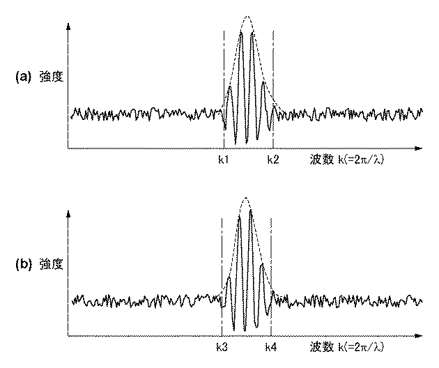
波長共焦点の原理によって、被検面100の近傍に集光点を形成する波数帯域の被検光のみが波長選択部112を通過し、参照光との干渉光(干渉信号)として検出することができる。従って、図2(a)では、干渉による周期的な信号を得ることができる波数帯域は、波数kL(kL=2π/λL)から波数kH(kH=2π/λH)のうち、被検面100の近傍に集光点を形成する波数k1から波数k2までの波数帯域である。波数k1から波数k2までの波数帯域以外の波数帯域の第1被検光は、波長選択部112で遮光されるため、参照光との干渉光(干渉信号)として検出することができない。
According to the principle of wavelength confocal, only the test light in the wave number band that forms a condensing point in the vicinity of the
同様に、図2(b)では、干渉による周期的な信号を得ることができる波数帯域は、被検面100の近傍に集光点を形成する波数k3から波数k4までの端数帯域である。波数k3から波数k4までの端数帯域以外の波数帯域の第2被検光は、波長選択部112で遮光されるため、参照光との干渉光(干渉信号)として検出することができない。
Similarly, in FIG. 2B, the wave number band in which a periodic signal due to interference can be obtained is a fractional band from the wave number k <b> 3 to the wave number k <b> 4 that forms a condensing point in the vicinity of the
上述したように、第1被検光と第2被検光とは、光学素子106の作用によって焦点距離が異なるため、同一の波長の光における集光点の位置は一致しない。詳細には、被検面100の近傍に集光点を形成する第1被検光の波数k1から波数k2と、被検面100の近傍に集光点を形成する第2被検光の波数k3から波数k4とは、互いに異なる波数である。例えば、k3、k4>k1、k2、或いは、k3、k4<k1、k2となるように、即ち、両者の波長帯域が一致しないように、光学素子106が構成されている。ここでは、k3、k4>k1、k2であるものとして説明する。
As described above, the first test light and the second test light have different focal lengths due to the action of the
波数kに対する周期的な干渉信号から、被検光と参照光との光路長差に対応する距離を算出する方法の一例を説明する。まず、干渉信号Iは、以下の式(2)で表される。 An example of a method for calculating the distance corresponding to the optical path length difference between the test light and the reference light from the periodic interference signal for the wave number k will be described. First, the interference signal I is expressed by the following equation (2).
式(2)において、Aは参照光の振幅強度、Bは被検光の振幅強度、φ’は干渉信号の位相、Mは干渉次数、φは±πの範囲に含まれる干渉信号の位相の端数成分(以下、「端数位相」と称する)、Lは被検光と参照光との光路長差に対応する距離である。ここでは、空間の屈折率を1とし、分散はないものとしている。 In Equation (2), A is the amplitude intensity of the reference light, B is the amplitude intensity of the test light, φ ′ is the phase of the interference signal, M is the order of interference, and φ is the phase of the interference signal included in the range of ± π. A fractional component (hereinafter referred to as “fractional phase”), L is a distance corresponding to the optical path length difference between the test light and the reference light. Here, it is assumed that the refractive index of the space is 1, and there is no dispersion.
非特許文献1に開示されているように、干渉信号Iを高速フーリエ変換(FFT)することによって、干渉信号の振幅のスペクトルのピーク周波数から距離Lを求めることができる。このようにしてピーク周波数を求める場合、干渉信号を得ることができる波数範囲が広ければ、ピーク周波数を高精度に求めることができる。但し、図2(a)に示すように、干渉信号を得ることができる波数範囲が狭い範囲に限定されると、誤差が生じやすく、ピーク周波数を高精度に求めることができない。従って、被検光と参照光との光路長差に対応する距離Lを高精度に求めることができない。
As disclosed in
そこで、第1の実施形態では、以下に説明する処理によって、被検光と参照光との光路長差に対応する距離を高精度に求めることを可能にしている。まず、図2(a)に示す干渉信号I1(以下、「第1干渉信号I1」と称する)を高速フーリエ変換(FFT)することによって、振幅スペクトルにおけるピーク周波数を決定し、かかるピーク周波数から距離L1を決定する。式(2)を参照するに、距離L1の2倍(2L1)は、図3に示すように、波数kに対する第1干渉信号I1の位相φ’の傾きに相当する。 Therefore, in the first embodiment, it is possible to obtain the distance corresponding to the optical path length difference between the test light and the reference light with high accuracy by the processing described below. First, the peak frequency in the amplitude spectrum is determined by performing fast Fourier transform (FFT) on the interference signal I 1 (hereinafter referred to as “first interference signal I 1 ”) shown in FIG. to determine the distance L 1 from. Referring to Equation (2), twice the distance L 1 (2L 1 ) corresponds to the slope of the phase φ ′ of the first interference signal I 1 with respect to the wave number k, as shown in FIG.
次に、距離L1を用いて第1干渉信号I1を離散フーリエ変換(DFT)することによって、任意の波数kにおける第1干渉信号I1の端数位相φを決定する。具体的には、第1干渉信号I1の端数位相φは、以下の式(3)で決定される。 Next, the fractional phase φ of the first interference signal I 1 at an arbitrary wave number k is determined by performing a discrete Fourier transform (DFT) on the first interference signal I 1 using the distance L 1 . Specifically, of fractional phase φ first interference signal I 1, it is determined by the following equation (3).
式(3)を参照するに、例えば、波数k1における端数位相φ1(φ1’=2πM1+φ1)や端数k2における端数位相φ2(φ2’=2πM2+φ2)など、波数k1から波数k2の間の任意の波数における端数位相(第1端数位相)を決定することができる。 Referring to Equation (3), for example, the wave number k1 such as the fractional phase φ 1 (φ 1 ′ = 2πM 1 + φ 1 ) at the wave number k1 and the fractional phase φ 2 (φ 2 ′ = 2πM 2 + φ 2 ) at the fraction k2 To a fractional phase (first fractional phase) at an arbitrary wavenumber between 1 and wavenumber k2.
次に、図2(b)に干渉信号I2(以下、「第2干渉信号I2」と称する)に対しても第1干渉信号I1と同様な処理を行い、第2干渉信号I2に基づいて距離L2を決定する。ここで、距離L2は距離L1と本質的に異なるため、補正処理が必要となる。被検光と参照光との光路長差に対応する距離とは、厳密には、参照光及び被検光が通過する経路における被検光と参照光との非共通な光路の距離の差である。 Next, in FIG. 2B, the same processing as that of the first interference signal I 1 is performed on the interference signal I 2 (hereinafter referred to as “second interference signal I 2 ”), and the second interference signal I 2 is performed. determining the distance L 2 on the basis of. Here, the distance L 2 is a distance L 1 which is essentially different order, the correction processing is required. Strictly speaking, the distance corresponding to the optical path length difference between the test light and the reference light is the difference between the non-common optical paths between the test light and the reference light in the path through which the reference light and the test light pass. is there.
図1において、参照面104と分割素子103との間の距離をT1、分割素子103から第1経路に沿って分割素子107までの間の距離をT2とする。また、分割素子107から被検面100までの間の距離をT3、分割素子103から第2経路に沿って分割素子107までの距離をT4とする。
In FIG. 1, the distance between the
第1被検光について、参照光との非共通光路の距離は、2×(T2+T3)である。また、参照光について、第1被検光との非共通光路の距離は、2×T1である。従って、第1被検光と参照光との光路長差に対応する距離は、2×(T2+T3−T1)である。 For the first test light, the distance of the non-common optical path from the reference light is 2 × (T2 + T3). In addition, the distance of the non-common optical path with respect to the reference light with respect to the first test light is 2 × T1. Therefore, the distance corresponding to the optical path length difference between the first test light and the reference light is 2 × (T2 + T3−T1).
一方、第2被検光について、参照光との非共通光路の距離は、2×(T4+T3)である。また、参照光について、第2被検光との非共通光路の距離は、2×T1である。従って、第2被検光と参照光との光路長差に対応する距離は、2×(T4+T3−T1)である。 On the other hand, for the second test light, the distance of the non-common optical path from the reference light is 2 × (T4 + T3). In addition, the distance of the non-common optical path with respect to the reference light with respect to the second test light is 2 × T1. Therefore, the distance corresponding to the optical path length difference between the second test light and the reference light is 2 × (T4 + T3−T1).
このように、第2被検光と参照光との光路長差に対応する距離は、第1被検光と参照光との光路長差に対応する距離より、2×(T4−T2)だけ異なる距離となる。ここで、T2及びT4は、計測装置10の内部構成の距離であるため、設計値や事前の計測などで取得可能であり、既知の量である。従って、これらを用いて、干渉信号から算出された距離L2をL2’に補正することが可能であり、補正式は、2×L2’=2×L2−2×(T4−T2)となる。かかる補正式に、2×L2=2×(T4+T3−T1)を代入すると明らかなように、計測誤差がなければ、L2’は、本質的には、2×L1=2×(T2+T3−T1)と等しくなる。
Thus, the distance corresponding to the optical path length difference between the second test light and the reference light is 2 × (T4−T2) than the distance corresponding to the optical path length difference between the first test light and the reference light. It will be a different distance. Here, since T2 and T4 are distances of the internal configuration of the measuring
また、第1経路又は第2経路において、折り曲げミラーなどを配置して光路を調整し、T4−T2=0となるように予め構成することによって、補正処理を省略することも可能である。 Further, it is possible to omit the correction process by arranging the folding mirror or the like in the first path or the second path to adjust the optical path so that T4−T2 = 0.
このようにして補正された距離L2’に基づいて、波数k3から波数k4の間の任意の波数における端数位相(第2端数位相)を決定する。ここでは、第2端数位相として、波数k3における端数位相φ3を決定するものとする。 Based on the distance L 2 ′ thus corrected, a fractional phase (second fractional phase) at an arbitrary wavenumber between the wavenumber k3 and the wavenumber k4 is determined. Here, as the second fractional phase, it shall determine the fractional phase phi 3 at wave numbers of k3.
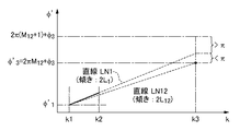
図4を参照して、補正された位相の傾きL12を決定する方法を説明する。図4において、直線LN1は、決定した波数k1における第1干渉信号I1の位相φ1’(φ1’=2πM1+φ1)及び位相の傾き2L1によって決定される直線である。また、干渉次数M1は、任意の値に設定してよい。直線LN2は、φ3’=2π(M12+M1)+φ3で表される位相φ3’と位相φ1’とによって決定される直線である。M12は、波数k1における第1干渉信号I1と波数k3における第2干渉信号I2との間の干渉次数差であり、以下の式(4)で表される。式(4)における「round( )」は、引数を整数に丸める関数を示す。 Referring to FIG. 4, a method of determining the slope L 12 of corrected phase. In FIG. 4, a straight line LN1 is a straight line determined by the phase φ 1 ′ (φ 1 ′ = 2πM 1 + φ 1 ) and the phase gradient 2L 1 of the first interference signal I 1 at the determined wave number k1. Further, the interference order M 1 may be set to an arbitrary value. The straight line LN2 is a straight line determined by the phase φ 3 ′ and the phase φ 1 ′ represented by φ 3 ′ = 2π (M 12 + M 1 ) + φ 3 . M 12 is a interference order difference between the second interference signal I 2 in the first interference signal I 1 and the wave number k3 in wavenumber k1, is represented by the following formula (4). “Round ()” in Expression (4) indicates a function for rounding an argument to an integer.
式(4)で決定したM12を用いて、直線LN2の傾きから距離L12を決定する。具体的には、距離L12は、以下の式(5)で決定される。 Using the M 12 determined in equation (4), determining the distance L 12 from the slope of the straight line LN2. Specifically, the distance L 12 is determined by the following equation (5).
このようにして決定した距離L12は、波数k1から波数k3の範囲で干渉信号が存在し、かかる干渉信号に基づいて算出した距離と同程度の精度を有する。従って、波数k1から波数k2までの干渉信号から算出した距離L1よりも波数の範囲が広がっているため、被検光と参照光との光路長差に対応する距離を高精度に求めることができる。 The distance L12 determined in this way has an interference signal in the range of the wave number k1 to the wave number k3, and has the same accuracy as the distance calculated based on the interference signal. Therefore, since the wave number range is wider than the distance L 1 calculated from the interference signals from the wave number k1 to the wave number k2, it is possible to obtain the distance corresponding to the optical path length difference between the test light and the reference light with high accuracy. it can.
また、本実施形態では、直線LN1を、波数k1における位相の傾き2L1によって決定される直線としたが、これに限定されるものではない。例えば、第2干渉信号I2について算出した位相の傾き2L3でもよいし、位相の傾きL1及びL3の平均値(2L1+2L3)/2でもよい。 Further, in the present embodiment, the straight line LN1, was a straight line is determined by the phase slope 2L 1 in wavenumber k1, but not limited thereto. For example, the phase gradient 2L 3 calculated for the second interference signal I 2 may be used, or the average value (2L 1 + 2L 3 ) / 2 of the phase gradients L 1 and L 3 may be used.
また、第1干渉信号I1及び第2干渉信号I2に対する処理は、上述した処理に限定されるものではない。互いに離散した複数の波長帯域での干渉信号を用いて、1つの波長帯域での干渉信号から距離を算出した場合よりも高精度に距離を算出する、という目的において変更が可能であり、例えば、特許文献1や非特許文献2に開示された技術を適用してもよい。
Further, processing for the first interference signal I 1 and the second interference signal I 2 is not limited to the above-described processing. For the purpose of calculating the distance with higher accuracy than the case of calculating the distance from the interference signal in one wavelength band using the interference signals in a plurality of wavelength bands that are discrete from each other, for example, The techniques disclosed in
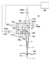
また、図1に示す計測装置10では、1つの参照面104を有するが、これに限定されるものではない。例えば、図5に示すように、計測装置10は、複数の参照面104a及び104bを有してもよい。図5は、本発明の第1の実施形態における計測装置10の別の構成を示す概略図である。
In addition, the
図5を参照するに、光源101からの光は、光学素子102によってコリメートされ、分割素子120に入射する。分割素子120は、光源101からの光を、分割素子103aに向かう光と、分割素子103bに向かう光とに分割する。以下では、説明を簡単にするために、分割素子103a、光学素子106、分割素子107、光学素子110及び被検面100を順に、或いは、逆に通過する経路を第3経路と称する。同様に、分割素子103b、分割素子107、光学素子110及び被検面100を順に、或いは、逆に通過する経路を第4経路と称する。
Referring to FIG. 5, the light from the
分割素子120から分割素子103aに向かう光は、分割素子103aによって、参照面104aに向かう第1参照光と、光学素子106に向かう第1被検光とに分割される。第1被検光は、第3経路において、光学的パワーを有する光学素子106によって屈折力を付加され、光学的パワーを有する光学素子110によって軸上色収差を付加される。これにより、第1被検光は、被検面100に対して、複数の波長のそれぞれで(即ち、波長ごとに)互いに異なる位置に集光点(像点)を形成する。被検面100で反射した第1被検光は、第3経路を通過し、光学素子111aを経て、波長選択部112aに入射する。一方、第1参照光は、参照面104aで反射し、分割素子103a及び光学素子111aを順に経て、波長選択部112aに入射する。
The light traveling from the
また、分割素子120から分割素子103bに向かう光は、分割素子103bによって、参照面104bに向かう第2参照光と、分割素子107に向かう第2被検光とに分割される。第2被検光は、第4経路において、光学素子110によって軸上色収差を付加され、被検面100に対して、複数の波長のそれぞれで(即ち、波長ごとに)互いに異なる位置に集光点(像点)を形成する。被検面100で反射した第2被検光は、第4経路を通過し、光学素子111bを経て、波長選択部112bに入射する。一方、第2参照光は、参照面104bで反射し、分割素子103b及び光学素子111bを順に経て、波長選択部112bに入射する。
The light traveling from the
波長選択部112aは、被検面100で反射した第1被検光が第3経路及び光学素子111aを順に経て波長選択部112aに入射する経路において、被検面側に形成された集光点と共役な関係となる位置に配置されたピンホールを有するピンホール板で構成される。波長選択部112bは、被検面100で反射した第2被検光が第4経路及び光学素子111bを順に経て波長選択部112bに入射する経路において、被検面側に形成された集光点と共役な関係となる位置に配置されたピンホールを有するピンホール板で構成される。
The
従って、被検面100で反射した第1被検光が第4経路を通過し、光学素子111bを経て波長選択部112bに入射しても、その経路における共役な位置は波長選択部112bの位置と異なる。これは、第4経路を通過し、光学素子111bを経る経路では、被検面100で反射した第1被検光が光学素子106を通過しないため、その分だけ焦点距離が異なるからである。従って、そのような経路を通過した第1被検光は、その殆どが波長選択部112bで遮光され、検出部113bには到達しない。
Therefore, even if the first test light reflected by the
同様に、被検面100で反射した第2被検光が第3経路を通過し、光学素子111aを経て波長選択部112aに入射しても、その経路における共役な位置は波長選択部112aの位置と異なる。これは、第3経路を通過し、光学素子111aを経る経路では、被検面100で反射した第2被検光が光学素子106を通過するため、その分だけ焦点距離が異なるからである。従って、そのような経路を通過した第2被検光は、その殆どが波長選択部112aで遮光され、検出部113aには到達しない。
Similarly, even if the second test light reflected by the
検出部113aには、波長選択部112aを介して、第1被検光と第1参照光との干渉光のみが入射する。また、検出部113bには、波長選択部112bを介して、第2被検光と第2参照光との干渉光のみが入射する。
Only the interference light between the first test light and the first reference light is incident on the
図5に示す計測装置10における被検光と参照光との光路長差に対応する距離について説明する。図5において、参照面104aと分割素子103aとの間の距離をT5、第3経路における分割素子103aから分割素子107までの間の距離をT6とする。また、分割素子107から被検面100までの間の距離をT7、参照面104bと分割素子103bとの間の距離をT8、第4経路における分割素子103bから分割素子107までの間の距離をT9とする。
The distance corresponding to the optical path length difference between the test light and the reference light in the
第1被検光について、第1参照光との非共通光路の距離は、2×(T6+T7)である。また、第1参照光について、第1被検光との非共通光路の距離は、2×T5である。従って、第1被検光と第1参照光との光路長差に対応する距離は、2×(T6+T7−T5)である。 For the first test light, the distance of the non-common optical path from the first reference light is 2 × (T6 + T7). Further, the distance of the non-common optical path with respect to the first test light with respect to the first reference light is 2 × T5. Therefore, the distance corresponding to the optical path length difference between the first test light and the first reference light is 2 × (T6 + T7−T5).
一方、第2被検光について、第2参照光との非共通光路の距離は、2×(T9+T7)である。また、第2参照光について、第2被検光との非共通光路の距離は、2×T8である。従って、第2被検光と第2参照光との光路長差に対応する距離は、2×(T9+T7−T8)である。 On the other hand, for the second test light, the distance of the non-common optical path from the second reference light is 2 × (T9 + T7). Further, the distance of the non-common optical path with respect to the second test light with respect to the second reference light is 2 × T8. Therefore, the distance corresponding to the optical path length difference between the second test light and the second reference light is 2 × (T9 + T7−T8).
このように、第2被検光と第2参照光との光路長差に対応する距離は、第1被検光と第1参照光との光路長差に対応する距離より、2×(T9−T8−T6+T5)だけ異なる距離となる。ここで、T5、T6、T8及びT9は、計測装置10の内部構成の距離であるため、設計値や事前の計測などで取得可能であり、既知の量である。従って、第2被検光及び第2参照光における被検光と参照光との光路長差に対応する距離は、2×L2’=2×L2−2×(T9−T8−T6+T5)で表される補正式で補正することが可能である。かかる補正式に、2×L2=2×(T9+T7−T8)を代入すると明らかなように、計測誤差がなければ、L2’は、本質的には、2×L1=2×(T6+T7−T5)と等しくなる。
Thus, the distance corresponding to the optical path length difference between the second test light and the second reference light is 2 × (T9) than the distance corresponding to the optical path length difference between the first test light and the first reference light. -T8-T6 + T5). Here, since T5, T6, T8, and T9 are distances of the internal configuration of the measuring
また、T9−T8−T6+T5=0となるように予め構成することによって、補正処理を省略することも可能である。ここで、図5に示す計測装置10では、参照面104aと参照面104bとが互いに独立して構成されているため、図1に示す計測装置10と比べて配置の自由度が高く、T9−T8−T6+T5=0となる構成への変更や調整が比較的容易である。
Further, the correction process can be omitted by configuring in advance such that T9−T8−T6 + T5 = 0. Here, in the
本実施形態では、被検光を2つの光に分割する構成を説明したが、これに限定されるものではない。例えば、被検光を3つ以上の光に分割し、3つ以上の被検光のそれぞれについて、焦点距離が異なる軸上色収差を有する構成であってもよい。被検光を複数の光に分割すれば、その波数分だけ干渉信号が得られるため、被検光と参照光との光路長差に対応する距離を更に高精度に計測することが可能となる。 In the present embodiment, the configuration in which the test light is divided into two lights has been described, but the present invention is not limited to this. For example, the configuration may be such that the test light is divided into three or more lights, and each of the three or more test lights has axial chromatic aberration with different focal lengths. If the test light is divided into a plurality of lights, interference signals corresponding to the number of waves can be obtained, so that the distance corresponding to the optical path length difference between the test light and the reference light can be measured with higher accuracy. .
また、本実施形態では、光学素子106によって第1被検光の焦点距離と第2被検光の焦点距離とを異ならせ、光学素子110によって第1被検光及び第2被検光のそれぞれに軸上色収差を付加しているが、これに限定されるものではない。それぞれの被検光に軸上色収差を付加して波長ごとに異なる位置に集光点を形成し、且つ、それぞれの被検光が同一波長において互いに異なる位置に集光点を形成するという目的において変更可能である。例えば、図1に示す計測装置10では、光学素子110の代わりに、第1経路及び第2経路の両方に、軸上色収差を有する光学系(光学素子)を配置してもよい。また、光学素子106及び光をコリメートする光学素子102の代わりに、光をコリメートしない光学素子を光学素子102の位置に配置し、第1経路と第2経路との距離差によって、同一波長での被検面側の集光点の位置を異ならせてもよい。一方、図5に示す計測装置10では、光学素子110の代わりに、第3経路及び第4経路の両方に、軸上色収差を有する光学系(光学素子)を配置してもよい。また、光学素子106及び光をコリメートする光学素子102の代わりに、光をコリメートしない光学素子を光学素子102の位置に配置し、第3経路と第4経路との距離差によって、同一波長での被検面側の集光点の位置を異ならせてもよい。
In the present embodiment, the
また、本実施形態では、全ての分割素子をビームスプリッターで構成しているが、これに限定されるものではない。例えば、分割素子は、光の偏光状態に応じて反射又は透過の特性が異なる分割素子、具体的には、偏光ビームスプリッター(PBS)などで構成してもよい。また、分割素子は、光の波長に応じて反射又は透過の特性が異なる分割素子、具体的には、ダイクロイックミラーやダイクロイックプリズムなどで構成してもよい。 In the present embodiment, all the splitting elements are configured by beam splitters, but the present invention is not limited to this. For example, the splitting element may be configured by a splitting element having different reflection or transmission characteristics depending on the polarization state of light, specifically, a polarization beam splitter (PBS) or the like. Further, the dividing element may be constituted by a dividing element having different reflection or transmission characteristics depending on the wavelength of light, specifically, a dichroic mirror or a dichroic prism.
図1に示す計測装置10において、分割素子としてダイクロイックミラーを適用する場合を考える。この場合、分割素子105及び107は、波長λC(λL<λC<λH)よりも短い波長の光を反射し、波長λC’(λL<λC<λC’<λH)よりも長い波長の光を透過する特性を有するダイクロイックミラーで構成される。従って、第1被検光については、光学素子106の屈折力によって、波長λC’の光が位置P01に集光点を形成し、波長λHの光が位置P02に集光点を形成する。一方、第2被検光については、波長λLの光が位置P11に集光点を形成し、波長λCの光が位置P12に集光点を形成する。ここで、ダイクロイックミラーの作用により、第1被検光と第2被検光とは同一の波長を有していないため、光学素子106の屈折力を調整して位置P01と位置P11とが同一の位置となるようにしてもよい。同様に、光学素子106の屈折力を調整して位置P02と位置P12とが同一の位置となるようにしてもよい。
Consider a case where a dichroic mirror is applied as a splitting element in the measuring
このような構成によって、被検面100で反射した第1被検光及び第2被検光は、反射前と同等の経路を通過して分割素子103に到達するため、波長選択部112に入射する計測誤差の要因となる不要光を低減することができる。また、分割素子をビームスプリッターで構成した場合には、計測可能レンジは位置P11から位置P02であるが、分割素子をダイクロイックミラーで構成した場合には、計測可能レンジを位置P01から位置P12に広げることが可能となる。
With such a configuration, the first test light and the second test light reflected by the
同様に、図5に示す計測装置10において、分割素子としてダイクロイックミラーを適用する場合を考える。この場合、分割素子120及び107は、波長λC(λL<λC<λH)よりも短い波長の光を反射し、波長λC’(λL<λC<λC’<λH)よりも長い波長の光を透過する特性を有するダイクロイックミラーで構成される。このような構成によって、計測誤差の要因となる不要光を低減することができる。
Similarly, consider a case where a dichroic mirror is applied as a splitting element in the
また、分割素子としてPBSを用いても、計測誤差の要因となる不要光を低減することが可能である。例えば、図1に示す計測装置10において、分割素子としてPBSを適用する場合を考える。この場合、分割素子105及び107がPBSで構成される。PBSの作用によって、第1経路における分割素子105から分割素子107まではP偏光の光しか通過することができず、第2経路における分割素子105から分割素子107まではS偏光の光しか通過することができない。従って、第1経路を通過する第1被検光は、被検面100で反射した後、第2経路を通過することができない。同様に、第2経路を通過する第2被検光は、検面100で反射した後、第1経路を通過することができない。これにより、波長選択部112に入射する計測誤差の要因となる不要光を低減することができる。
Further, even if PBS is used as the dividing element, it is possible to reduce unnecessary light that causes measurement errors. For example, consider a case where PBS is applied as a dividing element in the
同様に、図5に示す計測装置10において、分割素子としてPBSを適用する場合を考える。この場合、分割素子120及び107がPBSで構成される。このような構成によって、計測誤差の要因となる不要光を低減することができる。
Similarly, consider a case in which PBS is applied as a dividing element in the
分割素子にダイクロイックミラーを適用した場合には、波長によって被検光の光路を分離して、被検光のそれぞれが被検面100での反射前と反射後において異なる経路を通過することを抑制し、計測誤差となる不要光を低減している。一方、分割素子にPBSを適用した場合には、偏光によって被検光の光路を分離して、被検光のそれぞれが被検面100での反射前と反射後において異なる経路を通過することを抑制し、計測誤差となる不要光を低減している。
When a dichroic mirror is applied to the dividing element, the optical path of the test light is separated according to the wavelength, and each of the test light is prevented from passing through different paths before and after reflection on the
<第2の実施形態>
図6は、本発明の第2の実施形態における計測装置10Aの構成を示す概略図である。計測装置10Aは、被検光と参照光との光路長差に対応する距離を計測する計測装置であって、例えば、波長走査干渉計の構成を有する。計測装置10Aは、複数の波長を含む波長帯域において射出する光の波長を変更可能な光源201と、光学素子102と、分割素子103と、参照面104と、分割素子105と、光学素子106と、分割素子107と、反射素子108及び109とを有する。また、計測装置10Aは、光学素子110と、光学素子111と、波長選択部112と、検出部202と、処理部203とを有する。
<Second Embodiment>
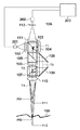
FIG. 6 is a schematic diagram showing a configuration of a
計測装置10Aは、波長をλHからλLまで連続的又は離散的に変更することが可能な光源201から射出した光を、光学素子110を介して、被検面100に照射する。また、計測装置10Aは、被検面100で反射した光と参照面104で反射した光との干渉光を検出部202で検出し、かかる干渉光から得られる干渉信号に基づいて、被検光と参照光との光路長差に対応する距離を処理部203で算出する。
The
光源201は、例えは、波長可変レーザーで構成され、供給電圧や供給電流などを変化させることによって波長を変更(走査)することが可能である。検出部202は、例えば、フォトダイオードなどの光センサで構成される。処理部203は、光源201から射出した光の波長、及び、光源201から射出される光の波長走査に応じて変化する干渉信号(各波長における干渉信号)に基づいて、被検光と参照光との光路長差に対応する距離を算出する。
The
計測装置10Aにおいて、光源201から射出した光が通過する経路、及び、分割素子で分割された光が通過する経路については、第1の実施形態において図1に示した計測装置10と同様である。図1に示す計測装置10は、光源101から複数の波長を含む光を射出し、検出部113で分光することによって、各波長における干渉信号を取得する分光干渉計の構成を有する。一方、図6に示す計測装置10Aは、光源201から射出される略単一波長の光の波長を走査することによって、各波長における干渉信号を取得する波長走査干渉計の構成を有する。従って、光源201から射出される光の波長の走査に応じて取得される干渉信号を、横軸に波数、縦軸に干渉信号の強度を採用して整列することによって、図2(a)に示す第1干渉信号I1及び図2(b)に示す第2干渉信号I2と同等の干渉信号が得られる。このようにして得られた第1干渉信号I1及び第2干渉信号I2に基づいて被検光と参照光との光路長差に対応する距離を算出する処理には、第1の実施形態で説明した処理を適用することができる。従って、計測装置10Aは、被検光と参照光との光路長差に対応する距離を高精度に計測することができる。
In the
図7は、本発明の第2の実施形態の計測装置10Aの別の構成を示す概略図である。ここで、図6に示す計測装置10Aは、図1に示す計測装置10に対応しているのに対して、図7に示す計測装置10Aは、図5に示す計測装置10に対応している。図7に示す計測装置10Aにおいて、光源201は、波長をλHからλLまで連続的又は離散的に変更することが可能である。また、検出部202a及び202bによって干渉光が検出され、かかる干渉光から得られる干渉信号に基づいて、被検光と参照光との光路長差に対応する距離を処理部115で算出する。
FIG. 7 is a schematic diagram showing another configuration of the
図7に示す計測装置10Aにおいて、光源201から射出した光が通過する経路、及び、第1参照光、第1被検光、第2参照光及び第2被検光が通過する経路については、第1の実施形態において図5に示した計測装置10と同様である。図7に示す計測装置10Aでは、参照面104aと参照面104bとが互いに独立して構成されているため、図6に示す計測装置10Aと比べて配置の自由度が高く、T9−T8−T6+T5=0となる構成への変更や調整が比較的容易である。
In the
また、本実施形態では、計測装置10Aにおける干渉信号の処理が第1の実施形態と同じであることを前提に説明したが、これに限定されるものではない。互いに離散した複数の波長帯域での干渉信号を用いて、1つの波長帯域での干渉信号から距離を算出した場合よりも高精度に距離を算出する、という目的において変更が可能であり、例えば、特許文献1や非特許文献2に開示された技術を適用してもよい。
In the present embodiment, the description has been made on the assumption that the processing of the interference signal in the
本実施形態では、被検光を2つの光に分割する構成を説明したが、これに限定されるものではない。例えば、被検光を3つ以上の光に分割し、3つ以上の被検光のそれぞれについて、焦点距離が異なる軸上色収差を有する構成であってもよい。被検光を複数の光に分割すれば、その波数分だけ干渉信号が得られるため、被検光と参照光との光路長差に対応する距離を更に高精度に計測することが可能となる。 In the present embodiment, the configuration in which the test light is divided into two lights has been described, but the present invention is not limited to this. For example, the configuration may be such that the test light is divided into three or more lights, and each of the three or more test lights has axial chromatic aberration with different focal lengths. If the test light is divided into a plurality of lights, interference signals corresponding to the number of waves can be obtained, so that the distance corresponding to the optical path length difference between the test light and the reference light can be measured with higher accuracy. .
また、本実施形態では、光学素子106によって第1被検光の焦点距離と第2被検光の焦点距離とを異ならせ、光学素子110によって第1被検光及び第2被検光のそれぞれに軸上色収差を付加しているが、これに限定されるものではない。それぞれの被検光に軸上色収差を付加して波長ごとに異なる位置に集光点を形成し、且つ、それぞれの被検光が同一波長において互いに異なる位置に集光点を形成するという目的において変更可能である。例えば、図6に示す計測装置10Aでは、光学素子110の代わりに、第1経路及び第2経路の両方に、軸上色収差を有する光学系(光学素子)を配置してもよい。また、光学素子106及び光をコリメートする光学素子102の代わりに、光をコリメートしない光学素子を光学素子102の位置に配置し、第1経路と第2経路との距離差によって、同一波長での被検面側の集光点の位置を異ならせてもよい。一方、図7に示す計測装置10Aでは、光学素子110の代わりに、第3経路及び第4経路の両方に、軸上色収差を有する光学系(光学素子)を配置してもよい。また、光学素子106及び光をコリメートする光学素子102の代わりに、光をコリメートしない光学素子を光学素子102の位置に配置し、第3経路と第4経路との距離差によって、同一波長での被検面側の集光点の位置を異ならせてもよい。
In the present embodiment, the
また、本実施形態では、全ての分割素子をビームスプリッターで構成しているが、これに限定されるものではない。例えば、分割素子は、光の偏光状態に応じて反射又は透過の特性が異なる分割素子、具体的には、偏光ビームスプリッター(PBS)などで構成してもよい。また、分割素子は、光の波長に応じて反射又は透過の特性が異なる分割素子、具体的には、ダイクロイックミラーやダイクロイックプリズムなどで構成してもよい。 In the present embodiment, all the splitting elements are configured by beam splitters, but the present invention is not limited to this. For example, the splitting element may be configured by a splitting element having different reflection or transmission characteristics depending on the polarization state of light, specifically, a polarization beam splitter (PBS) or the like. Further, the dividing element may be constituted by a dividing element having different reflection or transmission characteristics depending on the wavelength of light, specifically, a dichroic mirror or a dichroic prism.
図6に示す計測装置10Aにおいて、分割素子としてダイクロイックミラーを適用する場合を考える。この場合、分割素子105及び107は、波長λC(λL<λC<λH)よりも短い波長の光を反射し、波長λC’(λL<λC<λC’<λH)よりも長い波長の光を透過する特性を有するダイクロイックミラーで構成される。従って、第1被検光については、光学素子106の屈折力によって、波長λC’の光が位置P01に集光点を形成し、波長λHの光が位置P02に集光点を形成する。一方、第2被検光については、波長λLの光が位置P11に集光点を形成し、波長λCの光が位置P12に集光点を形成する。ここで、ダイクロイックミラーの作用により、第1被検光と第2被検光とは同一の波長を有していないため、光学素子106の屈折力を調整して位置P01と位置P11とが同一の位置となるようにしてもよい。同様に、光学素子106の屈折力を調整して位置P02と位置P12とが同一の位置となるようにしてもよい。
Consider a case where a dichroic mirror is applied as a dividing element in the
このような構成によって、被検面100で反射した第1被検光及び第2被検光は、反射前と同等の経路を通過して分割素子103に到達するため、波長選択部112に入射する計測誤差の要因となる不要光を低減することができる。また、分割素子をビームスプリッターで構成した場合には、計測可能レンジは位置P11から位置P02であるが、分割素子をダイクロイックミラーで構成した場合には、計測可能レンジを位置P01から位置P12に広げることが可能となる。
With such a configuration, the first test light and the second test light reflected by the
同様に、図7に示す計測装置10Aにおいて、分割素子としてダイクロイックミラーを適用する場合を考える。この場合、分割素子120及び107は、波長λC(λL<λC<λH)よりも短い波長の光を反射し、波長λC’(λL<λC<λC’<λH)よりも長い波長の光を透過する特性を有するダイクロイックミラーで構成される。このような構成によって、計測誤差の要因となる不要光を低減することができる。
Similarly, consider a case where a dichroic mirror is applied as a dividing element in the
また、分割素子としてPBSを用いても、計測誤差の要因となる不要光を低減することが可能である。例えば、図6に示す計測装置10Aにおいて、分割素子としてPBSを適用する場合を考える。この場合、分割素子105及び107がPBSで構成される。PBSの作用によって、第1経路における分割素子105から分割素子107まではP偏光の光しか通過することができず、第2経路における分割素子105から分割素子107まではS偏光の光しか通過することができない。従って、第1経路を通過する第1被検光は、被検面100で反射した後、第2経路を通過することができない。同様に、第2経路を通過する第2被検光は、検面100で反射した後、第1経路を通過することができない。これにより、波長選択部112に入射する計測誤差の要因となる不要光を低減することができる。
Further, even if PBS is used as the dividing element, it is possible to reduce unnecessary light that causes measurement errors. For example, consider a case where PBS is applied as a dividing element in the
同様に、図7に示す計測装置10Aにおいて、分割素子としてPBSを適用する場合を考える。この場合、分割素子120及び107がPBSで構成される。このような構成によって、計測誤差の要因となる不要光を低減することができる。
Similarly, consider a case where PBS is applied as a dividing element in the
分割素子にダイクロイックミラーを適用した場合には、波長によって被検光の光路を分離して、被検光のそれぞれが被検面100での反射前と反射後において異なる経路を通過することを抑制し、計測誤差となる不要光を低減している。一方、分割素子にPBSを適用した場合には、偏光によって被検光の光路を分離して、被検光のそれぞれが被検面100での反射前と反射後において異なる経路を通過することを抑制し、計測誤差となる不要光を低減している。
When a dichroic mirror is applied to the dividing element, the optical path of the test light is separated according to the wavelength, and each of the test light is prevented from passing through different paths before and after reflection on the
以上、本発明の好ましい実施形態について説明したが、本発明はこれらの実施形態に限定されないことはいうまでもなく、その要旨の範囲内で種々の変形及び変更が可能である。 As mentioned above, although preferable embodiment of this invention was described, it cannot be overemphasized that this invention is not limited to these embodiment, A various deformation | transformation and change are possible within the range of the summary.
Claims (12)
光源から射出された光から分割される第1被検光及び第2被検光のうち、前記第1被検光が通過する第1光学系、及び、前記第2被検光が通過する第2光学系と、
被検面で反射された前記第1被検光及び前記第2被検光のそれぞれと参照面で反射された参照光との干渉光を検出する検出部と、
前記検出部で検出された干渉光に基づいて、前記距離を求める処理部と、
を有し、
前記第1光学系における光学的パワーと前記第2光学系における光学的パワーとが異なり、
前記第1被検光の前記被検面側の集光点と前記被検面との間の距離は、複数の波長のそれぞれに応じて互いに異なり、
前記第2被検光の前記被検面側の集光点と前記被検面との間の距離は、複数の波長のそれぞれに応じて互いに異なり、
前記集光点と前記被検面との間の距離が所定距離となる集光点に対応する波長の前記第1被検光及び前記第2被検光のそれぞれを前記検出部に導く導光部を更に有することを特徴とする計測装置。 A measuring device that measures a distance corresponding to an optical path length difference between test light and reference light,
Of the first test light and the second test light that are split from the light emitted from the light source, the first optical system through which the first test light passes and the second test light through which the second test light passes through. Two optical systems;
A detection unit that detects interference light between each of the first test light and the second test light reflected by the test surface and the reference light reflected by the reference surface;
A processing unit for obtaining the distance based on the interference light detected by the detection unit;
Have
The optical power in the first optical system is different from the optical power in the second optical system,
The distance between the focusing point on the test surface side of the first test light and the test surface is different from each other according to each of a plurality of wavelengths,
The distance between the focusing point on the test surface side of the second test light and the test surface is different from each other according to each of a plurality of wavelengths,
A light guide that guides each of the first test light and the second test light having a wavelength corresponding to a condensing point at which the distance between the condensing point and the test surface is a predetermined distance to the detection unit. The measuring device further comprising a section.
前記導光部は、前記共通部分に配置されていることを特徴とする請求項1に記載の計測装置。 The first optical system and the second optical system include a common part in which a part of the path of the first test light and a part of the path of the second test light are common,
The measuring apparatus according to claim 1, wherein the light guide unit is disposed in the common part.
前記共通部分には、前記第1被検光及び前記第2被検光に対して同一の軸上色収差を有する光学素子が配置されていることを特徴とする請求項2に記載の計測装置。 The portions of the first optical system excluding the common portion and the portions of the second optical system excluding the common portion have different focal lengths with respect to the first test light and the second test light. An optical element having
The measuring apparatus according to claim 2, wherein an optical element having the same axial chromatic aberration with respect to the first test light and the second test light is disposed in the common portion.
前記検出部で検出された前記第1被検光と前記参照光との干渉光から得られる第1干渉信号に基づいて、前記第1干渉信号の位相の傾きである第1位相の傾きと、前記第1干渉信号に含まれる任意の波数における前記第1干渉信号の位相である第1位相の端数成分とを求め、
前記検出部で検出された前記第2被検光と前記参照光との干渉光から得られる第2干渉信号に基づいて、前記第2干渉信号に含まれる任意の波数における前記第2干渉信号の位相である第2位相の端数成分を求め、
前記第1位相の傾きと、前記第1位相の端数成分と、前記第2の位相の端数成分とに基づいて、前記第1位相と前記第2位相との間の干渉次数差である第1干渉次数差を求め、
前記第1干渉次数差と、前記第1位相の端数成分と、前記第2位相の端数成分とに基づいて、前記距離を求めることを特徴とする請求項1乃至9のうちいずれか1項に記載の計測装置。 The processor is
Based on a first interference signal obtained from interference light between the first test light and the reference light detected by the detection unit, a first phase gradient that is a phase gradient of the first interference signal; Obtaining a fractional component of the first phase that is the phase of the first interference signal at an arbitrary wave number included in the first interference signal;
Based on the second interference signal obtained from the interference light between the second test light and the reference light detected by the detection unit, the second interference signal at an arbitrary wave number included in the second interference signal. Find the fractional component of the second phase, which is the phase,
A first interference order difference between the first phase and the second phase based on the slope of the first phase, the fractional component of the first phase, and the fractional component of the second phase. Find the interference order difference,
10. The distance according to claim 1, wherein the distance is obtained based on the first interference order difference, the fractional component of the first phase, and the fractional component of the second phase. The measuring device described.
前記検出部で検出された前記第1被検光と前記参照光との干渉光から得られる第1干渉信号に基づいて、前記第1干渉信号の位相の傾きである第1位相の傾きと、前記第1干渉信号に含まれる任意の波数における前記第1干渉信号の位相である第1位相の端数成分を求め、
前記検出部で検出された前記第2被検光と前記参照光との干渉光から得られる第2干渉信号に基づいて、前記第2干渉信号の位相の傾きである第2位相の傾きと、前記第2干渉信号に含まれる任意の波数における前記第2干渉信号の位相である第2位相の端数成分とを求め、
前記第1位相の傾きと、前記第1位相の端数成分と、前記第2位相の傾きと、前記第2位相の端数成分とに基づいて、前記第1位相と前記第2位相との間の干渉次数差である第1干渉次数差を求め、
前記第1干渉次数差と、前記第1位相の端数成分と、前記第2位相の端数成分とに基づいて、前記距離を求めることを特徴とする請求項1乃至9のうちいずれか1項に記載の計測装置。 The processor is
Based on a first interference signal obtained from interference light between the first test light and the reference light detected by the detection unit, a first phase gradient that is a phase gradient of the first interference signal; Obtaining a fractional component of the first phase that is the phase of the first interference signal at an arbitrary wave number included in the first interference signal;
Based on the second interference signal obtained from the interference light between the second test light and the reference light detected by the detection unit, a second phase gradient that is a phase gradient of the second interference signal; Determining a fractional component of the second phase that is the phase of the second interference signal at an arbitrary wave number included in the second interference signal;
Based on the slope of the first phase, the fractional component of the first phase, the slope of the second phase, and the fractional component of the second phase, between the first phase and the second phase Obtaining a first interference order difference which is an interference order difference;
10. The distance according to claim 1, wherein the distance is obtained based on the first interference order difference, the fractional component of the first phase, and the fractional component of the second phase. The measuring device described.
前記1つの位相の傾きと、前記2つの位相の端数成分とに基づいて、前記第1干渉信号及び前記第2干渉信号のそれぞれの間の干渉次数差を求め、
前記干渉次数差と、前記2つの位相の端数成分とに基づいて、前記距離を求めることを特徴とする請求項1乃至9のうちいずれか1項に記載の計測装置。 The processing unit includes a first interference signal obtained from an interference light between the first test light detected by the detection unit and the reference light, and the second test light detected by the detection unit. Based on the second interference signal obtained from the interference light with the reference light, one phase gradient which is a phase gradient of the first interference signal and the second interference signal, the first interference signal and the first interference signal Determining a fractional component of two phases that are phases of the first interference signal and the second interference signal at an arbitrary wave number included in two interference signals;
Based on the slope of the one phase and the fractional component of the two phases, an interference order difference between each of the first interference signal and the second interference signal is obtained,
The measuring apparatus according to claim 1, wherein the distance is obtained based on the interference order difference and a fractional component of the two phases.
Priority Applications (2)
| Application Number | Priority Date | Filing Date | Title |
|---|---|---|---|
| JP2013079924A JP2014202645A (en) | 2013-04-05 | 2013-04-05 | Measuring instrument |
| US14/242,949 US20140300904A1 (en) | 2013-04-05 | 2014-04-02 | Measurement apparatus |
Applications Claiming Priority (1)
| Application Number | Priority Date | Filing Date | Title |
|---|---|---|---|
| JP2013079924A JP2014202645A (en) | 2013-04-05 | 2013-04-05 | Measuring instrument |
Publications (1)
| Publication Number | Publication Date |
|---|---|
| JP2014202645A true JP2014202645A (en) | 2014-10-27 |
Family
ID=51654227
Family Applications (1)
| Application Number | Title | Priority Date | Filing Date |
|---|---|---|---|
| JP2013079924A Pending JP2014202645A (en) | 2013-04-05 | 2013-04-05 | Measuring instrument |
Country Status (2)
| Country | Link |
|---|---|
| US (1) | US20140300904A1 (en) |
| JP (1) | JP2014202645A (en) |
Families Citing this family (2)
| Publication number | Priority date | Publication date | Assignee | Title |
|---|---|---|---|---|
| WO2019120470A1 (en) * | 2017-12-18 | 2019-06-27 | Universität Stuttgart | Method and assembly for chromatic confocal spectral interferometry or spectral domain oct |
| WO2025190490A1 (en) | 2024-03-15 | 2025-09-18 | Universität Stuttgart | An optical system and a method for chromatic confocal spectral-domain optical coherence tomography with a plurality of wavelets or for chromatic confocal two-beam interferometry |
Family Cites Families (3)
| Publication number | Priority date | Publication date | Assignee | Title |
|---|---|---|---|---|
| DE102005006723B3 (en) * | 2005-02-03 | 2006-06-08 | Universität Stuttgart | Interferometrical confocal method for optical data memory e.g. terabyte volume memory, involves transmitting light from multi-wavelength source and arranging spectrometer in front of screened receiver |
| KR101819006B1 (en) * | 2010-10-27 | 2018-01-17 | 삼성전자주식회사 | Optical measuring apparatus |
| US8587772B2 (en) * | 2011-12-21 | 2013-11-19 | Mitutoyo Corporation | Chromatic point sensor configuration including real time spectrum compensation |
-
2013
- 2013-04-05 JP JP2013079924A patent/JP2014202645A/en active Pending
-
2014
- 2014-04-02 US US14/242,949 patent/US20140300904A1/en not_active Abandoned
Also Published As
| Publication number | Publication date |
|---|---|
| US20140300904A1 (en) | 2014-10-09 |
Similar Documents
| Publication | Publication Date | Title |
|---|---|---|
| US7170610B2 (en) | Low-coherence inferometric device for light-optical scanning of an object | |
| JP7408265B2 (en) | confocal displacement meter | |
| JP5882674B2 (en) | Multi-wavelength interferometer, measuring apparatus and measuring method | |
| TWI670465B (en) | Confocal measurement device | |
| KR20130039005A (en) | Three dimensional depth and shape measuring device | |
| JP5648961B2 (en) | Spectral characteristic measuring apparatus and calibration method thereof | |
| JP2010014426A (en) | Measuring device | |
| JP2012058068A5 (en) | ||
| KR101251292B1 (en) | Three dimensional shape and depth measuring device using polarized light | |
| US20120105861A1 (en) | Device and method for determining optical path lengths | |
| JP2020535433A (en) | Non-contact methods and devices for measuring the distance to a surface or the distance between two surfaces | |
| KR20110077598A (en) | Interference System and Measurement System Using Partial Reflection | |
| EP2718666A1 (en) | Coupled multi-wavelength confocal systems for distance measurements | |
| JP2013152191A (en) | Multi-wavelength interferometer | |
| US20140160490A1 (en) | Interference measuring apparatus and interference measuring method | |
| JP5740701B2 (en) | Interferometer | |
| KR101620594B1 (en) | spectroscopy apparatus | |
| JP2010025922A (en) | Interference device | |
| JP5772783B2 (en) | Optical tomographic image acquisition device | |
| JP2014202645A (en) | Measuring instrument | |
| KR101078197B1 (en) | Polarized Point Diffraction Interferometer for Optical System Alignment | |
| JP2000186912A (en) | Method and apparatus for measuring small displacement | |
| CN114719983B (en) | Space heterodyne Raman spectrometer | |
| WO2017104661A1 (en) | Spectroscope, optical inspection device, and oct device | |
| JP7812916B2 (en) | Optical Thickness Measurement Device |