JP2014084506A - Substrate processing method, substrate processing device, and program - Google Patents
Substrate processing method, substrate processing device, and program Download PDFInfo
- Publication number
- JP2014084506A JP2014084506A JP2012235048A JP2012235048A JP2014084506A JP 2014084506 A JP2014084506 A JP 2014084506A JP 2012235048 A JP2012235048 A JP 2012235048A JP 2012235048 A JP2012235048 A JP 2012235048A JP 2014084506 A JP2014084506 A JP 2014084506A
- Authority
- JP
- Japan
- Prior art keywords
- gas
- source gas
- processing chamber
- wafer
- raw material
- Prior art date
- Legal status (The legal status is an assumption and is not a legal conclusion. Google has not performed a legal analysis and makes no representation as to the accuracy of the status listed.)
- Pending
Links
- 239000000758 substrate Substances 0.000 title claims abstract description 138
- 238000012545 processing Methods 0.000 title claims description 313
- 238000003672 processing method Methods 0.000 title claims description 29
- 239000007789 gas Substances 0.000 claims abstract description 674
- 239000003446 ligand Substances 0.000 claims abstract description 215
- 239000002994 raw material Substances 0.000 claims abstract description 173
- 238000000034 method Methods 0.000 claims abstract description 101
- 239000012495 reaction gas Substances 0.000 claims abstract description 83
- 238000000354 decomposition reaction Methods 0.000 claims abstract description 39
- 230000001737 promoting effect Effects 0.000 claims abstract description 13
- 239000012528 membrane Substances 0.000 claims abstract description 5
- 230000008569 process Effects 0.000 claims description 78
- 235000012431 wafers Nutrition 0.000 description 176
- 239000010408 film Substances 0.000 description 158
- 238000010926 purge Methods 0.000 description 54
- 229910000618 GeSbTe Inorganic materials 0.000 description 48
- 238000012546 transfer Methods 0.000 description 39
- 229910052751 metal Inorganic materials 0.000 description 38
- 239000002184 metal Substances 0.000 description 38
- 239000011261 inert gas Substances 0.000 description 35
- 239000012159 carrier gas Substances 0.000 description 32
- 238000010586 diagram Methods 0.000 description 32
- 229910052732 germanium Inorganic materials 0.000 description 30
- 229910052714 tellurium Inorganic materials 0.000 description 25
- 229910052787 antimony Inorganic materials 0.000 description 24
- 239000000203 mixture Substances 0.000 description 24
- 230000015572 biosynthetic process Effects 0.000 description 19
- 239000004065 semiconductor Substances 0.000 description 18
- 239000007788 liquid Substances 0.000 description 17
- 230000008016 vaporization Effects 0.000 description 17
- 230000007246 mechanism Effects 0.000 description 14
- 238000003860 storage Methods 0.000 description 14
- 239000006185 dispersion Substances 0.000 description 13
- 229910052739 hydrogen Inorganic materials 0.000 description 12
- 239000000463 material Substances 0.000 description 12
- 230000000694 effects Effects 0.000 description 11
- 238000011144 upstream manufacturing Methods 0.000 description 11
- GNPVGFCGXDBREM-UHFFFAOYSA-N germanium atom Chemical compound [Ge] GNPVGFCGXDBREM-UHFFFAOYSA-N 0.000 description 9
- 239000001257 hydrogen Substances 0.000 description 9
- 230000004048 modification Effects 0.000 description 9
- 238000012986 modification Methods 0.000 description 9
- IJGRMHOSHXDMSA-UHFFFAOYSA-N Atomic nitrogen Chemical compound N#N IJGRMHOSHXDMSA-UHFFFAOYSA-N 0.000 description 8
- 238000004140 cleaning Methods 0.000 description 8
- 229910052757 nitrogen Inorganic materials 0.000 description 8
- 239000002245 particle Substances 0.000 description 8
- 238000009834 vaporization Methods 0.000 description 8
- UFHFLCQGNIYNRP-UHFFFAOYSA-N Hydrogen Chemical compound [H][H] UFHFLCQGNIYNRP-UHFFFAOYSA-N 0.000 description 7
- 229910052799 carbon Inorganic materials 0.000 description 7
- 229910052735 hafnium Inorganic materials 0.000 description 7
- 239000012535 impurity Substances 0.000 description 7
- 229910052760 oxygen Inorganic materials 0.000 description 7
- 229910052726 zirconium Inorganic materials 0.000 description 7
- QGZKDVFQNNGYKY-UHFFFAOYSA-N Ammonia Chemical compound N QGZKDVFQNNGYKY-UHFFFAOYSA-N 0.000 description 6
- 230000005587 bubbling Effects 0.000 description 6
- 238000006243 chemical reaction Methods 0.000 description 6
- 238000000926 separation method Methods 0.000 description 6
- 229910052719 titanium Inorganic materials 0.000 description 6
- 239000006227 byproduct Substances 0.000 description 5
- 230000003197 catalytic effect Effects 0.000 description 5
- 238000009792 diffusion process Methods 0.000 description 5
- 230000003028 elevating effect Effects 0.000 description 5
- 238000010438 heat treatment Methods 0.000 description 5
- 238000011084 recovery Methods 0.000 description 5
- 239000010409 thin film Substances 0.000 description 5
- OKTJSMMVPCPJKN-UHFFFAOYSA-N Carbon Chemical compound [C] OKTJSMMVPCPJKN-UHFFFAOYSA-N 0.000 description 4
- WATWJIUSRGPENY-UHFFFAOYSA-N antimony atom Chemical compound [Sb] WATWJIUSRGPENY-UHFFFAOYSA-N 0.000 description 4
- QVGXLLKOCUKJST-UHFFFAOYSA-N atomic oxygen Chemical compound [O] QVGXLLKOCUKJST-UHFFFAOYSA-N 0.000 description 4
- 230000006870 function Effects 0.000 description 4
- 239000011344 liquid material Substances 0.000 description 4
- 238000004519 manufacturing process Methods 0.000 description 4
- 239000001301 oxygen Substances 0.000 description 4
- 229910052710 silicon Inorganic materials 0.000 description 4
- PORWMNRCUJJQNO-UHFFFAOYSA-N tellurium atom Chemical compound [Te] PORWMNRCUJJQNO-UHFFFAOYSA-N 0.000 description 4
- VYPSYNLAJGMNEJ-UHFFFAOYSA-N Silicium dioxide Chemical compound O=[Si]=O VYPSYNLAJGMNEJ-UHFFFAOYSA-N 0.000 description 3
- 229910004356 Ti Raw Inorganic materials 0.000 description 3
- 229910021529 ammonia Inorganic materials 0.000 description 3
- 239000013078 crystal Substances 0.000 description 3
- 238000009826 distribution Methods 0.000 description 3
- 238000011068 loading method Methods 0.000 description 3
- 229910052752 metalloid Inorganic materials 0.000 description 3
- 230000002093 peripheral effect Effects 0.000 description 3
- 239000000126 substance Substances 0.000 description 3
- OAKJQQAXSVQMHS-UHFFFAOYSA-N Hydrazine Chemical compound NN OAKJQQAXSVQMHS-UHFFFAOYSA-N 0.000 description 2
- XUIMIQQOPSSXEZ-UHFFFAOYSA-N Silicon Chemical compound [Si] XUIMIQQOPSSXEZ-UHFFFAOYSA-N 0.000 description 2
- 230000009471 action Effects 0.000 description 2
- OPDQOJBKHNWJGO-UHFFFAOYSA-N butylgermane Chemical group CCCC[GeH3] OPDQOJBKHNWJGO-UHFFFAOYSA-N 0.000 description 2
- 230000008859 change Effects 0.000 description 2
- 150000002431 hydrogen Chemical class 0.000 description 2
- 238000002156 mixing Methods 0.000 description 2
- TWNQGVIAIRXVLR-UHFFFAOYSA-N oxo(oxoalumanyloxy)alumane Chemical compound O=[Al]O[Al]=O TWNQGVIAIRXVLR-UHFFFAOYSA-N 0.000 description 2
- 239000010453 quartz Substances 0.000 description 2
- 239000010703 silicon Substances 0.000 description 2
- 229910018072 Al 2 O 3 Inorganic materials 0.000 description 1
- PIGFYZPCRLYGLF-UHFFFAOYSA-N Aluminum nitride Chemical compound [Al]#N PIGFYZPCRLYGLF-UHFFFAOYSA-N 0.000 description 1
- 206010067482 No adverse event Diseases 0.000 description 1
- ATJFFYVFTNAWJD-UHFFFAOYSA-N Tin Chemical compound [Sn] ATJFFYVFTNAWJD-UHFFFAOYSA-N 0.000 description 1
- 230000002411 adverse Effects 0.000 description 1
- 229910052782 aluminium Inorganic materials 0.000 description 1
- XAGFODPZIPBFFR-UHFFFAOYSA-N aluminium Chemical compound [Al] XAGFODPZIPBFFR-UHFFFAOYSA-N 0.000 description 1
- YENXDKGOGVLOPS-UHFFFAOYSA-N butane-1-tellurol Chemical group CCCC[TeH] YENXDKGOGVLOPS-UHFFFAOYSA-N 0.000 description 1
- 239000000919 ceramic Substances 0.000 description 1
- 239000007795 chemical reaction product Substances 0.000 description 1
- 238000005229 chemical vapour deposition Methods 0.000 description 1
- 238000004891 communication Methods 0.000 description 1
- PMHQVHHXPFUNSP-UHFFFAOYSA-M copper(1+);methylsulfanylmethane;bromide Chemical compound Br[Cu].CSC PMHQVHHXPFUNSP-UHFFFAOYSA-M 0.000 description 1
- 230000008878 coupling Effects 0.000 description 1
- 238000010168 coupling process Methods 0.000 description 1
- 238000005859 coupling reaction Methods 0.000 description 1
- 238000000151 deposition Methods 0.000 description 1
- 230000008021 deposition Effects 0.000 description 1
- RAABOESOVLLHRU-UHFFFAOYSA-N diazene Chemical compound N=N RAABOESOVLLHRU-UHFFFAOYSA-N 0.000 description 1
- 229910000071 diazene Inorganic materials 0.000 description 1
- -1 diisopropyl tellurium Chemical compound 0.000 description 1
- 238000010790 dilution Methods 0.000 description 1
- 239000012895 dilution Substances 0.000 description 1
- YMUZFVVKDBZHGP-UHFFFAOYSA-N dimethyl telluride Chemical compound C[Te]C YMUZFVVKDBZHGP-UHFFFAOYSA-N 0.000 description 1
- 238000005530 etching Methods 0.000 description 1
- ILXWFJOFKUNZJA-UHFFFAOYSA-N ethyltellanylethane Chemical compound CC[Te]CC ILXWFJOFKUNZJA-UHFFFAOYSA-N 0.000 description 1
- 238000011049 filling Methods 0.000 description 1
- 238000004518 low pressure chemical vapour deposition Methods 0.000 description 1
- 239000007769 metal material Substances 0.000 description 1
- ZUSRFDBQZSPBDV-UHFFFAOYSA-N n-[bis(dimethylamino)stibanyl]-n-methylmethanamine Chemical compound CN(C)[Sb](N(C)C)N(C)C ZUSRFDBQZSPBDV-UHFFFAOYSA-N 0.000 description 1
- 150000004767 nitrides Chemical class 0.000 description 1
- 231100000989 no adverse effect Toxicity 0.000 description 1
- 230000003287 optical effect Effects 0.000 description 1
- 230000003647 oxidation Effects 0.000 description 1
- 238000007254 oxidation reaction Methods 0.000 description 1
- 230000004044 response Effects 0.000 description 1
- 229910021332 silicide Inorganic materials 0.000 description 1
- FVBUAEGBCNSCDD-UHFFFAOYSA-N silicide(4-) Chemical compound [Si-4] FVBUAEGBCNSCDD-UHFFFAOYSA-N 0.000 description 1
- HBMJWWWQQXIZIP-UHFFFAOYSA-N silicon carbide Chemical compound [Si+]#[C-] HBMJWWWQQXIZIP-UHFFFAOYSA-N 0.000 description 1
- 229910001220 stainless steel Inorganic materials 0.000 description 1
- 239000010935 stainless steel Substances 0.000 description 1
- 230000003746 surface roughness Effects 0.000 description 1
- 229910052715 tantalum Inorganic materials 0.000 description 1
- QQRKOFXRIWEHIV-UHFFFAOYSA-N tert-butyl(dimethyl)stibane Chemical compound C[Sb](C)C(C)(C)C QQRKOFXRIWEHIV-UHFFFAOYSA-N 0.000 description 1
- 238000005979 thermal decomposition reaction Methods 0.000 description 1
- RBEXEKTWBGMBDZ-UHFFFAOYSA-N tri(propan-2-yl)stibane Chemical compound CC(C)[Sb](C(C)C)C(C)C RBEXEKTWBGMBDZ-UHFFFAOYSA-N 0.000 description 1
- KKOFCVMVBJXDFP-UHFFFAOYSA-N triethylstibane Chemical compound CC[Sb](CC)CC KKOFCVMVBJXDFP-UHFFFAOYSA-N 0.000 description 1
Images


Landscapes
- Chemical Vapour Deposition (AREA)
Abstract
Description
本発明は、基板処理方法、基板処理装置およびプログラムに関する。 The present invention relates to a substrate processing method, a substrate processing apparatus, and a program.
半導体装置(デバイス)の製造工程の一工程として、シリコンウエハ等の基板上に、例えばゲルマニウム(Ge)等の所定元素を含む膜(Ge膜)を形成する成膜工程が行われることがある。Ge膜は、基板を収容した減圧雰囲気下にある処理室内にGe原料ガスを供給し、処理室内でGe原料ガスの熱分解反応を生じさせて基板上にGeを堆積させる減圧CVD(Chemical Vapor Deposition)法によって成膜することができる。 As one process of manufacturing a semiconductor device (device), a film forming process for forming a film (Ge film) containing a predetermined element such as germanium (Ge) on a substrate such as a silicon wafer may be performed. The Ge film is a low-pressure CVD (Chemical Vapor Deposition) in which a Ge source gas is supplied into a processing chamber under a reduced-pressure atmosphere containing a substrate, and a Ge source gas is pyrolyzed in the processing chamber to deposit Ge on the substrate. ) Method.
上述の方法では、処理室内に供給されたGe原料ガスが基板上で熱分解することで、Ge原料ガスに含まれるGeが基板上に吸着、堆積し、基板上にGe膜が形成される。しかしながら、係る方法では、基板上に形成されるGe膜の平坦性が低下してしまうことがある。 In the above-described method, the Ge source gas supplied into the processing chamber is thermally decomposed on the substrate, whereby Ge contained in the Ge source gas is adsorbed and deposited on the substrate, and a Ge film is formed on the substrate. However, with such a method, the flatness of the Ge film formed on the substrate may deteriorate.
そこで本発明は、基板上に形成する所定元素を含む膜の平坦性を向上させることが可能な基板処理方法、基板処理装置およびプログラムを提供することを目的とする。 Therefore, an object of the present invention is to provide a substrate processing method, a substrate processing apparatus, and a program capable of improving the flatness of a film containing a predetermined element formed on a substrate.
本発明の一態様によれば、
基板に対して、所定元素と、該所定元素に結合するリガンドと、が同一平面上に配置されてなる構造を有する原料ガスを供給する工程と、
前記基板に対して、前記原料ガスの分解を促進させる反応ガスを供給する工程と、
を含むサイクルを所定回数行うことで、前記基板上に、前記所定元素を含む膜を形成する工程を有する基板処理方法が提供される。
According to one aspect of the invention,
Supplying a raw material gas having a structure in which a predetermined element and a ligand bonded to the predetermined element are arranged on the same plane to the substrate;
Supplying a reaction gas that promotes decomposition of the source gas to the substrate;
A substrate processing method including a step of forming a film containing the predetermined element on the substrate by performing a cycle including the predetermined number of times is provided.
本発明の他の態様によれば、
基板に対して処理が行われる処理室と、
前記処理室内にガスを供給するガス供給系と、
前記処理室内の基板に対して、所定元素と、該所定元素に結合するリガンドと、が同一平面上に配置されてなる構造を有する原料ガスを供給する処理と、前記処理室内の前記基板に対して、前記原料ガスの分解を促進させる反応ガスを供給する処理と、を含むサイクルを所定回数行うことで、前記基板上に、前記所定元素を含む膜を形成する処理を行うように、前記ガス供給系を制御するよう構成される制御部と、
を有する基板処理装置が提供される。
According to another aspect of the invention,
A processing chamber in which processing is performed on the substrate;
A gas supply system for supplying gas into the processing chamber;
A process of supplying a source gas having a structure in which a predetermined element and a ligand bonded to the predetermined element are arranged on the same plane with respect to the substrate in the processing chamber; The process of forming a film containing the predetermined element on the substrate is performed by performing a cycle including a process including supplying a reaction gas for promoting decomposition of the source gas a predetermined number of times. A controller configured to control the supply system;
A substrate processing apparatus is provided.
本発明のさらに他の態様によれば、
基板処理装置の処理室内の基板に対して、所定元素と、該所定元素に結合するリガンドと、が同一平面上に配置されてなる構造を有する原料ガスを供給する手順と、
前記処理室内の前記基板に対して、前記原料ガスの分解を促進させる反応ガスを供給する手順と、
を含むサイクルを所定回数行うことで、前記基板上に、前記所定元素を含む膜を形成する手順をコンピュータに実行させるプログラムが提供される。
According to yet another aspect of the invention,
Supplying a source gas having a structure in which a predetermined element and a ligand bonded to the predetermined element are arranged on the same plane to a substrate in a processing chamber of the substrate processing apparatus;
A procedure for supplying a reaction gas that promotes decomposition of the source gas to the substrate in the processing chamber;
A program for causing a computer to execute a procedure for forming a film containing the predetermined element on the substrate by performing a predetermined number of cycles including:
本発明に係る基板処理方法、基板処理装置およびプログラムによれば、基板上に形成する所定元素を含む膜の平坦性を向上させることが可能となる。 According to the substrate processing method, the substrate processing apparatus, and the program according to the present invention, it is possible to improve the flatness of a film containing a predetermined element formed on a substrate.
<本発明の第1実施形態>
(1)基板処理装置の構成
まず、本実施形態にかかる基板処理装置の構成について、図2〜4を参照しながら説明する。図2は、本実施形態にかかる基板処理装置40のウエハ処理時における断面構成図であり、図3は、本実施形態にかかる基板処理装置40のウエハ搬送時における断面構成図である。図4は、本実施形態で好適に用いられる基板処理装置40のコントローラ280の概略構成図である。
<First Embodiment of the Present Invention>
(1) Configuration of Substrate Processing Apparatus First, the configuration of the substrate processing apparatus according to the present embodiment will be described with reference to FIGS. FIG. 2 is a cross-sectional configuration diagram of the
(処理室)
図2,3に示されているとおり、本実施形態にかかる基板処理装置40は処理容器202を備えている。処理容器202は、例えば横断面が円形であり扁平な密閉容器として構成されている。また、処理容器202は、例えばアルミニウム(Al)やステンレス(SUS)などの金属材料により構成されている。処理容器202内には、基板としてのシリコンウエハ等のウエハ200に対して処理が行われる処理室201が形成されている。
(Processing room)
As shown in FIGS. 2 and 3, the
(支持台)
処理室201内には、ウエハ200を支持する支持台203が設けられている。ウエハ200が直接触れる支持台203の上面には、例えば、石英(SiO2)、カーボン、セラミックス、炭化ケイ素(SiC)、酸化アルミニウム(Al2O3)、又は窒化アルミニウム(AlN)などから構成された支持板としてのサセプタ217が設けられている。また、支持台203には、ウエハ200を加熱する加熱手段(加熱源)としてのヒータ206と、温度検出器としての温度センサ206bとが内蔵されている。温度センサ206bにより検出された温度情報に基づきヒータ206への通電具合を調整することで、サセプタ217上に支持されたウエハ200の温度が所望の温度分布となるように構成されている。なお、支持台203の下端部は、処理容器202の底部を貫通している。
(Support stand)
A
(昇降機構)
処理室201の外部には、支持台203を昇降させる昇降機構207bが設けられている。この昇降機構207bを作動させて支持台203を昇降させることにより、サセプタ217上に支持されるウエハ200を昇降させることが可能となっている。支持台203は、ウエハ200の搬送時には図3で示される位置(ウエハ搬送位置)まで下降し、ウエハ200の処理時には図2で示される位置(ウエハ処理位置)まで上昇する。なお、支持台203下端部の周囲は、ベローズ203aにより覆われており、処理室201内は気密に保持されている。
(Elevating mechanism)
Outside the
(リフトピン)
また、処理室201の底面(床面)には、例えば3本のリフトピン208bが鉛直方向に立ち上がるように設けられている。また、支持台203(サセプタ217も含む)には、かかるリフトピン208bを貫通させる貫通孔208aが、リフトピン208bに対応する位置にそれぞれ設けられている。そして、支持台203をウエハ搬送位置まで下降させた時には、図3に示されているように、リフトピン208bの上端部がサセプタ217の上面から突出して、リフトピン208bがウエハ200を下方から支持するようになっている。また、支持台203をウエハ処理位置まで上昇させたときには、図2に示されているようにリフトピン208bはサセプタ217の上面から埋没して、サセプタ217がウエハ200を下方から支持するようになっている。なお、リフトピン208bは、ウエハ200と直接触れるため、例えば、石英や酸化アルミニウムなどの材質で形成することが望ましい。
(Lift pin)
In addition, on the bottom surface (floor surface) of the
(ウエハ搬送口)
処理室201(処理容器202)の内壁側面には、処理室201の内外にウエハ200を搬送するウエハ搬送口250が設けられている。ウエハ搬送口250にはゲートバルブ44が設けられており、ゲートバルブ44を開くことにより、処理室201内と負圧移載室11内とが連通するようになっている。負圧移載室11は搬送容器(密閉容器)12内に形成されており、負圧移載室11内にはウエハ200を搬送する負圧移載機13が設けられている。負圧移載機13には、ウエハ200を搬送する際にウエハ200を支持する搬送アーム13aが備えられている。支持台203をウエハ搬送位置まで下降させた状態で、ゲートバルブ44を開くことにより、負圧移載機13により処理室201内と負圧移載室11内との間でウエハ200を搬送することが可能となっている。すなわち、負圧移載機13は、ウエハ200を処理室201内外に搬送する搬送装置(搬送機構)として構成される。処理室201内に搬送されたウエハ200は、上述したようにリフトピン208b上に一時的に載置される。なお、負圧移載室11のウエハ搬送口250が設けられた側と反対側には、図示しないロードロック室が設けられており、負圧移載機13によりロードロック室内と負圧移載室11内との間でウエハ200を搬送することが可能となっている。なお、ロードロック室は、未処理もしくは処理済のウエハ200を一時的に収容する予備室として機能する。
(Wafer transfer port)
On the inner wall side surface of the processing chamber 201 (processing container 202), a
(排気系)
処理室201(処理容器202)の内壁側面であって、ウエハ搬送口250の反対側には、処理室201内の雰囲気を排気する排気口260が設けられている。排気口260には、排気チャンバ260aを介して排気管261が接続されている。排気チャンバ260aには、処理室201内の圧力を検出する圧力検出器(圧力検出部)としての圧力センサ265が設けられている。排気管261には、処理室201内の圧力を所定の圧力とするように制御する圧力調整器(圧力調整部)としてのAPC(Auto Pressure Controller)バルブ262および原料回収トラップ263を介して、真空排気装置としての真空ポンプ264が接続されている。なお、APCバルブ262は、真空ポンプ264を作動させた状態で弁を開閉することで、処理室201内の真空排気および真空排気停止を行うことができ、更に、真空ポンプ264を作動させた状態で弁開度を調節することで、処理室201内の圧力を調整することができるように構成されているバルブである。主に、排気チャンバ260a、圧力センサ265、排気管261、APCバルブ262により排気系(排気ライン)が構成される。なお、原料回収トラップ263、真空ポンプ264を排気系に含めて考えてもよい。排気系は、真空ポンプ264を作動させつつ、圧力センサ265により検出された圧力情報に基づいてAPCバルブ262の弁の開度を調節することにより、処理室201内の圧力が所定の圧力(真空度)となるよう真空排気し得るように構成されている。
(Exhaust system)
An
(ガス供給口)
処理室201の上部に設けられる後述のシャワーヘッド240の上面(天井壁)には、処理室201内に所定元素を含む原料ガスを供給する原料ガス供給口210aと、処理室201内に原料ガスの分解を促進させる反応ガスを供給する反応ガス供給口210bと、が設けられている。つまり、反応ガス供給口210bは、原料ガス供給口210aとは独立して設けられており、原料ガスと反応ガスとは異なる供給口より別々に処理室201内へ供給されるように構成されている。なお、図2、図3には、反応ガス供給口210bを原料ガス供給口210aの内側に原料ガス供給口210aと同心円状に配置する構成を例示しているが、本発明は係る態様に限定されず、反応ガス供給口210bを原料ガス供給口210aの外側に設けてもよい。なお、原料ガス供給口210a、反応ガス供給口210bに接続される各ガス供給系の構成については後述する。
(Gas supply port)
On the upper surface (ceiling wall) of a shower head 240 (described later) provided in the upper portion of the
(シャワーヘッド)
原料ガス供給口210aと処理室201との間には、ガス分散機構としてのシャワーヘッド240が設けられている。シャワーヘッド240は、原料ガス供給口210aから供給される原料ガスを分散させる分散板240aと、分散板240aを通過した原料ガスをさらに均一に分散させて支持台203上のウエハ200の表面に供給するシャワー板240bと、を備えている。分散板240aおよびシャワー板240bには、それぞれ、複数の通気孔が設けられている。分散板240aは、シャワーヘッド240の上面及びシャワー板240bと対向するように配置されており、シャワー板240bは、支持台203上のウエハ200と対向するように配置されている。なお、シャワーヘッド240の上面と分散板240aとの間、および分散板240aとシャワー板240bとの間には、それぞれ空間が設けられており、かかる空間は、原料ガス供給口210aから供給される原料ガスを分散させる第1バッファ空間(分散室)240c、および分散板240aを通過した原料ガスを拡散させる第2バッファ空間(拡散室)240dとしてそれぞれ機能する。
(shower head)
A
なお、反応ガス供給口210bは、シャワーヘッド240を鉛直方向(厚さ方向)に貫通し、反応ガス供給口210bの下端開口がシャワー板240bの下面から支持台203に向けて突出するように設けられている。すなわち、反応ガス供給口210bは、反応ガスを、シャワー板240bの下方側から、つまり、シャワーヘッド240を介さずに処理室201内に供給するように構成されている。
The reaction
(排気ダクト)
処理室201(処理容器202)の内壁側面には、段差部201aが設けられている。そして、この段差部201aは、コンダクタンスプレート204をウエハ処理位置近傍に保持するように構成されている。コンダクタンスプレート204は、内周部にウエハ200を収容する穴が設けられた1枚のドーナツ状(リング状)をした円板として構成されている。コンダクタンスプレート204の外周部には、所定間隔を空けて周方向に配列された複数の排出口204aが設けられている。排出口204aは、コンダクタンスプレート204の外周部がコンダクタンスプレート204の内周部を支えることができるよう、不連続に形成されている。
(Exhaust duct)
A
一方、支持台203の外周部には、ロワープレート205が係止している。ロワープレート205は、リング状の凹部205bと、凹部205bの内側上部に一体的に設けられたフランジ部205aとを備えている。凹部205bは、支持台203の外周部と、処理室201の内壁側面との隙間を塞ぐように設けられている。凹部205bの底部のうち排気口260付近の一部には、凹部205b内から排気口260側へガスを排出(流通)させるプレート排気口205cが設けられている。フランジ部205aは、支持台203の上部外周縁上に係止する係止部として機能する。フランジ部205aが支持台203の上部外周縁上に係止することにより、ロワープレート205が、支持台203の昇降に伴い、支持台203と共に昇降されるようになっている。
On the other hand, a
支持台203がウエハ処理位置まで上昇したとき、ロワープレート205もウエハ処理位置まで上昇する。その結果、ウエハ処理位置近傍に保持されているコンダクタンスプレート204が、ロワープレート205の凹部205bの上面部分を塞ぎ、凹部205bの内部をガス流路領域とする排気ダクト259が形成されることとなる。なお、このとき、排気ダクト259(コンダクタンスプレート204及びロワープレート205)及び支持台203によって、処理室201内が、排気ダクト259よりも上方の処理室201上部と、排気ダクト259よりも下方の処理室201下部と、に仕切られることとなる。なお、コンダクタンスプレート204およびロワープレート205は、排気ダクト259の内壁に堆積する反応生成物をエッチングする場合(セルフクリーニングする場合)を考慮して、高温保持が可能な材料、例えば、耐高温高負荷用石英で構成することが好ましい。
When the support table 203 is raised to the wafer processing position, the
ここで、ウエハ処理時における処理室201内のガスの流れについて説明する。
Here, the flow of gas in the
まず、原料ガス供給口210aからシャワーヘッド240の上部へと供給された原料ガスは、第1バッファ空間(分散室)240cを経て分散板240aの複数の通気孔から第2バッファ空間240dへと入り、さらにシャワー板240bの複数の通気孔を通過して処理室201内に供給される。また、反応ガス供給口210bから供給された反応ガスは、シャワー板240bの下方側から、つまり、シャワーヘッド240を介さずに処理室201内に供給される。すなわち、原料ガス供給口210aから供給される原料ガスと、反応ガス供給口210bから供給される反応ガスとは、別々に処理室201内へ供給されることとなる。なお、原料ガスと反応ガスとが処理室201内に同時に供給される場合は、原料ガスと反応ガスとは、事前に混合されることなく処理室201内で初めて混合されることとなる。
First, the source gas supplied from the source
原料ガスと反応ガスは、それぞれウエハ200上に均一に供給され、ウエハ200の径方向外側に向かって放射状に流れる。そして、ウエハ200に接触した後の余剰なガスは、ウエハ200外周部に位置する排気ダクト259上、すなわち、コンダクタンスプレート204上を、ウエハ200の径方向外側に向かって放射状に流れ、コンダクタンスプレート204に設けられた排出口204aから、排気ダクト259内のガス流路領域内(凹部205b内)へと排出される。その後、ガスは排気ダクト259内を流れ、プレート排気口205cを経由して排気口260へと排気される。このようにガスを流すことで、処理室201下部、すなわち、支持台203の裏面や処理室201の底面側へのガスの回り込みが抑制される。
The source gas and the reaction gas are respectively uniformly supplied onto the
続いて、上述した原料ガス供給口210a、反応ガス供給口210bに接続されるガス供給系の構成について、図1を参照しながら説明する。図1は、本実施形態にかかる基板処理装置40の有するガス供給系(ガス供給ライン)の構成図である。
Next, the configuration of the gas supply system connected to the above-described source
本実施形態にかかる基板処理装置40の有するガス供給系は、常温常圧下で液体状態である液体原料を気化する気化部としてのバブラ220a,220b,220cと、バブラ220a,220b,220cにて液体原料を気化させて生成した各原料ガスを処理室201内に供給する原料ガス供給系と、処理室201内に反応ガスを供給する反応ガス供給系と、処理室201内に不活性ガスを供給する不活性ガス供給系と、を有している。さらに、基板処理装置40は、バブラ220a,220b,220cからの原料ガスを処理室201内に供給することなく処理室201をバイパスするよう排気するベント(バイパス)系を有している。以下に、各部の構成について説明する。
The gas supply system of the
(バブラ)
処理室201の外部には、液体原料を収容する原料容器としてのバブラ220a,220b,220cが設けられている。バブラ220a,220b,220cは、内部に液体原料を収容(充填)可能なタンク(密閉容器)として構成されており、また、液体原料をバブリングにより気化させて原料ガスを生成させる気化部としても構成されている。なお、バブラ220a,220b,220cの周りには、バブラ220a,220b,220cおよび内部の液体原料を加熱するサブヒータ206aが設けられている。
(Bubbler)
Outside the
バブラ220a,220b,220cには、それぞれ異なる所定元素を含む原料が収容されている。なお、ここでいう所定元素とは、金属元素、半金属元素および半導体元素のうち少なくともいずれかの元素を含む。本実施形態においては、バブラ220aには、第1の所定元素を含む第1の原料として、例えば、ゲルマニウム(Ge)を含むゲルマニウム原料(Ge原料)が収容されている。また、バブラ220bには、第2の所定元素を含む第2の原料として、例えば、アンチモン(Sb)を含むアンチモン原料(Sb原料)が収容されている。また、バブラ220cには、第3の所定元素を含む第3の原料として、例えば、テルル(Te)を含むテルル原料(Te原料)が収容されている。なお、ここで用いるGe原料、Sb原料、Te原料は、それぞれ常温常圧下で液体状態である。なお、本明細書において「原料」という言葉を用いた場合は、「液体状態である液体原料」を意味する場合、「液体原料を気化した原料ガス」を意味する場合、または、その両方を意味する場合がある。
The
バブラ220a,220b,220cには、それぞれ、キャリアガス供給管237a,237b,237cが接続されている。キャリアガス供給管237a,237b,237cの上流側端部には、それぞれ、図示しないキャリアガス供給源が接続されている。また、キャリアガス供給管237a,237b,237cの下流側端部は、それぞれ、バブラ220a,220b,220c内に収容した液体原料内に浸されている。
Carrier
キャリアガス供給管237aには、キャリアガスの供給流量を制御する流量制御器としてのマスフローコントローラ(MFC)222aと、キャリアガスの供給を制御するバルブva1,va2とが設けられている。また、キャリアガス供給管237bには、キャリアガスの供給流量を制御する流量制御器としてのマスフローコントローラ(MFC)222bと、キャリアガスの供給を制御するバルブvb1,vb2とが設けられている。また、キャリアガス供給管237cには、キャリアガスの供給流量を制御する流量制御器としてのマスフローコントローラ(MFC)222cと、キャリアガスの供給を制御するバルブvc1,vc2とが設けられている。
The carrier
なお、キャリアガスとしては、液体原料とは反応しないガスを用いることが好ましく、例えばN2ガスやArガスやHeガス等の不活性ガスが好適に用いられる。主に、キャリアガス供給管237a,237b,237c、MFC222a,222b,222c、バルブva1,va2,vb1,vb2,vc1,vc2により、キャリアガス供給系(キャリアガス供給ライン)が構成される。
As the carrier gas, a gas that does not react with the liquid raw material is preferably used. For example, an inert gas such as N 2 gas, Ar gas, or He gas is preferably used. A carrier gas supply system (carrier gas supply line) is mainly configured by carrier
上記構成により、バルブva1,va2を開き、キャリアガス供給管237aからMFC222aで流量制御されたキャリアガスをバブラ220a内に供給することにより、バブラ220a内部に収容された液体原料(Ge原料)をバブリングにより気化させて、第1の所定元素を含む第1の原料ガス、すなわち、Geを含むGe原料ガス(Ge含有ガス)を生成させることが可能となる。
With the above configuration, the valves va1 and va2 are opened, and the carrier gas whose flow rate is controlled by the
また、バルブvb1,vb2を開き、キャリアガス供給管237bからMFC222bで流量制御されたキャリアガスをバブラ220b内に供給することにより、バブラ220b内部に収容された液体原料(Sb原料)をバブリングにより気化させて、第2の所定元素を含む第2の原料ガス、すなわち、Sbを含むSb原料ガス(Sb含有ガス)を生成させることが可能となる。
Further, by opening the valves vb1 and vb2 and supplying the carrier gas whose flow rate is controlled by the
また、バルブvc1,vc2を開き、キャリアガス供給管237cからMFC222cで流量制御されたキャリアガスをバブラ220c内に供給することにより、バブラ220c内部に収容された液体原料(Te原料)をバブリングにより気化させて、第3の所定元素を含む第3の原料ガス、すなわち、Teを含むTe原料ガス(Te含有ガス)を生成させることが可能となる。
Further, by opening the valves vc1 and vc2 and supplying the carrier gas whose flow rate is controlled by the MFC 222c from the carrier
なお、後述するように、ウエハ200上に形成する膜の平坦性を向上させるには、成膜に用いる原料ガスとして、所定元素と、該所定元素に結合するリガンドと、が同一平面上に配置されてなる構造を有するガスを用いるのが好ましい。ここでリガンドとは、所定元素と結合する物質であって、炭素(C)、水素(H)、酸素(O)および窒素(N)のうち少なくともいずれかの元素を含む物質をいう。また、1つの所定元素に複数のリガンドが結合している場合、これら複数のリガンドは全て同種の物質であってもよく、また、互いに異種の物質であってもよい。
As will be described later, in order to improve the flatness of a film formed on the
所定元素と、該所定元素に結合するリガンドと、が同一平面上に配置されてなる構造を有する原料ガスを生成するには、バブラ220a,220b,220c内に収容する原料として、原料に含まれる所定元素に結合するリガンドの数が3以下であるような原料を選択することが好ましく、さらには、各種原料に含まれる所定元素に結合するリガンドの数が2以下であるような原料を選択することがより好ましい。
In order to generate a raw material gas having a structure in which a predetermined element and a ligand bonded to the predetermined element are arranged on the same plane, the raw material is contained in the raw material as the raw material contained in the
仮に、所定元素に結合するリガンドの数が3を超えていると、所定元素と、該所定元素に結合するリガンドと、が同一平面上に配置されにくくなる。図14の(a)は、その組成式中(1分子中)におけるリガンド(R)の数が4であるGe原料の分子構造式を示す図であり、(b)は、その分子モデルを示す図であり、(c)は組成式中におけるリガンドの数が4であるGe原料の一例として、ターシャリーブチルゲルマン(Ge(t−C4H9)H3、略称:TBGe)の分子構造式を示す図である。図14に示されているように、その組成式中(1分子中)におけるリガンド(R)の数が4であると、所定元素(Ge)と、該Geと結合する4つのリガンド(R)のうち3つのリガンド(R)と、がたとえ同一平面上に配置されていたとしても(たとえ図中x−y平面上に配置されていたとしても)、残りの1つのリガンド(R)が立体的に配置され易くなる(図中y−z平面上等に配置され易くなる)。すなわち、所定元素に結合するリガンドの数が3を超えていると、所定元素と、該所定元素に結合するリガンドと、が立体的に配置されてなる立体構造を有する傾向が強くなる。このような原料を選択した場合、所定元素と、該所定元素に結合するリガンドと、が同一平面上に配置されてなる構造を有する原料ガスを生成することは困難となる。 If the number of ligands binding to the predetermined element exceeds 3, the predetermined element and the ligand binding to the predetermined element are difficult to be arranged on the same plane. (A) of FIG. 14 is a diagram showing a molecular structural formula of a Ge raw material in which the number of ligands (R) in the composition formula (in one molecule) is 4, and (b) shows a molecular model thereof. a diagram, as an example of a Ge raw material number of ligand is 4 in (c) is in the composition formula, tertiary butyl germane (Ge (t-C 4 H 9) H 3, abbreviation: TBGe) molecular structural formula FIG. As shown in FIG. 14, when the number of ligands (R) in the composition formula (in one molecule) is 4, a predetermined element (Ge) and four ligands (R) that bind to the Ge Even if three of the ligands (R) are arranged on the same plane (even if arranged on the xy plane in the figure), the remaining one ligand (R) is a three-dimensional structure. It becomes easy to arrange | position (it becomes easy to arrange | position on a yz plane etc. in a figure). That is, if the number of ligands that bind to the predetermined element exceeds 3, the tendency to have a three-dimensional structure in which the predetermined element and the ligand that binds to the predetermined element are three-dimensionally arranged increases. When such a raw material is selected, it is difficult to generate a raw material gas having a structure in which a predetermined element and a ligand bonded to the predetermined element are arranged on the same plane.
これに対し、所定元素に結合するリガンドの数が3であると、所定元素と、該所定元素に結合するリガンドと、が同一平面上に配置され易くなる。図13(a)は、その組成式中(1分子中)におけるリガンド(R)の数が3であるGe原料の分子構造式を示す図であり、(b)は、その分子モデルを示す図である。図13に示されているように、その組成式中(1分子中)におけるリガンド(R)の数が3であると、所定元素(Ge)と、該Geと結合する3つのリガンド(R)と、が同一平面上(図中x−y平面上)に配置され易くなる。すなわち、所定元素に結合するリガンドの数が3であると、所定元素と、該所定元素に結合するリガンドと、が同一平面上に配置されてなる平面構造を有する傾向が強くなる。このような原料を選択した場合、所定元素と、該所定元素に結合するリガンドと、が同一平面上に配置されてなる構造を有する原料ガスを生成することが容易となる。 On the other hand, when the number of ligands binding to the predetermined element is 3, the predetermined element and the ligand binding to the predetermined element are easily arranged on the same plane. FIG. 13A is a diagram showing a molecular structural formula of a Ge raw material in which the number of ligands (R) in the composition formula (in one molecule) is 3, and FIG. 13B is a diagram showing a molecular model thereof. It is. As shown in FIG. 13, when the number of ligands (R) in the composition formula (in one molecule) is 3, a predetermined element (Ge) and three ligands (R) bonded to the Ge Are easily arranged on the same plane (on the xy plane in the figure). That is, when the number of ligands that bind to the predetermined element is 3, there is a strong tendency to have a planar structure in which the predetermined element and the ligand that binds to the predetermined element are arranged on the same plane. When such a raw material is selected, it becomes easy to generate a raw material gas having a structure in which a predetermined element and a ligand bonded to the predetermined element are arranged on the same plane.
また、所定元素に結合するリガンドの数が2以下であると、所定元素と、該所定元素に結合するリガンドと、が常に同一平面上に配置されることとなる。図12(a)および(b)は、その組成式中(1分子中)におけるリガンド(R)の数が2であるGe原料の分子構造式を示す図であり、(c)は、その分子モデルを示す図である。図12に示されているように、その組成式中(1分子中)におけるリガンド(R)の数が2であると、所定元素(Ge)と、該Geと結合する2つのリガンド(R)と、が常に同一平面上(図中x−y平面上)に配置されることとなる。すなわち、所定元素に結合するリガンドの数が2以下である原料を選択した場合、所定元素と、該所定元素に結合するリガンドと、が同一平面上に配置されてなる構造を有する原料ガスを、常に生成することができるようになる。 Further, when the number of ligands binding to the predetermined element is 2 or less, the predetermined element and the ligand binding to the predetermined element are always arranged on the same plane. 12 (a) and 12 (b) are diagrams showing the molecular structural formula of a Ge raw material in which the number of ligands (R) in the composition formula (in one molecule) is 2, and (c) shows the molecule It is a figure which shows a model. As shown in FIG. 12, when the number of ligands (R) in the composition formula (in one molecule) is 2, a predetermined element (Ge) and two ligands (R) that bind to the Ge Are always arranged on the same plane (on the xy plane in the figure). That is, when a raw material having two or less ligands bonded to a predetermined element is selected, a raw material gas having a structure in which the predetermined element and the ligand bonded to the predetermined element are arranged on the same plane, Can always be generated.
なお、原料に含まれる所定元素の原子価が4以上である場合において、所定元素に結合するリガンドの数を3以下とするには、所定元素とリガンドとの結合が二重結合以上の結合を含むような原料、すなわち、所定元素とリガンドとの結合が二重結合または三重結合もしくはそれ以上の結合を含むような原料を選択することが好ましい。 In the case where the valence of the predetermined element contained in the raw material is 4 or more, in order to reduce the number of ligands bonded to the predetermined element to 3 or less, the bond between the predetermined element and the ligand must be a double bond or more. It is preferable to select a raw material that contains a certain element, that is, a raw material in which a bond between a predetermined element and a ligand contains a double bond, a triple bond, or a bond higher than that.
例えば、Geのように原子価が4であるような元素を所定元素として含む原料を用いる場合、所定元素に結合するリガンドの数を3以下とするには、所定元素とリガンドとの結合が二重結合、または三重結合、もしくはそれ以上の結合を含むような原料を選択することが好ましい。 For example, when using a raw material containing an element having a valence of 4 as a predetermined element, such as Ge, in order to reduce the number of ligands bonded to the predetermined element to 3 or less, the bond between the predetermined element and the ligand is two. It is preferable to select a raw material that contains a heavy bond, a triple bond, or more.
具体的には、Geのように原子価が4である所定元素に結合するリガンドの数が3となるようにするには、図13(a)に示されているように、所定元素(Ge)と1つのリガンド(R)とが二重結合によって結合され、所定元素(Ge)と残りの2つのリガンド(R)とがそれぞれ一重結合によって結合されているような原料(Ge原料)を選択することが好ましい。このような原料を選択した場合、所定元素と、該所定元素に結合するリガンドと、が同一平面上に配置されてなる構造を有する原料ガスを生成することが容易となる。 Specifically, in order to set the number of ligands bonded to a predetermined element having a valence of 4 such as Ge to 3, the predetermined element (Ge) as shown in FIG. ) And one ligand (R) are bonded by a double bond, and a raw material (Ge raw material) in which a predetermined element (Ge) and the remaining two ligands (R) are bonded by a single bond is selected. It is preferable to do. When such a raw material is selected, it becomes easy to generate a raw material gas having a structure in which a predetermined element and a ligand bonded to the predetermined element are arranged on the same plane.
また、Geのように原子価が4である所定元素に結合するリガンドの数が2となるようにするには、図12(a)に示されているように、所定元素(Ge)と2つのリガンド(R)とがそれぞれ二重結合によって結合されているような原料(Ge原料)を選択したり、図12(b)に示されているように、所定元素(Ge)と2つのリガンド(R)とがそれぞれ一重結合と三重結合とによって結合されているような原料(Ge原料)を選択したりすることが好ましい。このような原料を選択した場合、所定元素と、該所定元素に結合するリガンドと、が同一平面上に配置されてなる構造を有する原料ガスを、常に生成することができるようになる。 In addition, in order to make the number of ligands bonded to a predetermined element having a valence of 4 such as Ge be two, as shown in FIG. 12A, the predetermined element (Ge) and 2 A raw material (Ge raw material) in which two ligands (R) are bonded to each other by a double bond is selected, or a predetermined element (Ge) and two ligands are selected as shown in FIG. It is preferable to select a raw material (Ge raw material) in which (R) is bonded to each other by a single bond and a triple bond. When such a raw material is selected, a raw material gas having a structure in which a predetermined element and a ligand bonded to the predetermined element are arranged on the same plane can always be generated.
また、例えば、Sbのように原子価が3であるような元素を所定元素として含む原料を用いる場合、所定元素に結合するリガンドの数は常に3以下となる。つまり、所定元素と、該所定元素に結合するリガンドと、が同一平面上に配置されてなる構造を有する原料ガスが生成され易くなる。なお、所定元素に結合するリガンドの数が2となるようにするには、所定元素とリガンドとの結合が二重結合を含むような原料を選択することが好ましい。すなわち、所定元素と2つのリガンドとのうちいずれかが二重結合によって結合され、残りが一重結合によって結合されているような原料を選択することが好ましい。このような原料を選択した場合、所定元素と、該所定元素に結合するリガンドと、が同一平面上に配置されてなる構造を有する原料ガスが、常に生成されるようになる。 For example, when a raw material containing an element having a valence of 3 as a predetermined element such as Sb is used, the number of ligands bonded to the predetermined element is always 3 or less. That is, it is easy to generate a source gas having a structure in which a predetermined element and a ligand that binds to the predetermined element are arranged on the same plane. In order to make the number of ligands bound to the predetermined element be 2, it is preferable to select a raw material in which the bond between the predetermined element and the ligand includes a double bond. That is, it is preferable to select a raw material in which one of the predetermined element and the two ligands is bonded by a double bond and the remaining is bonded by a single bond. When such a raw material is selected, a raw material gas having a structure in which a predetermined element and a ligand bonded to the predetermined element are arranged on the same plane is always generated.
また、例えば、Teのように原子価が2であるような元素を所定元素として含む原料を用いる場合、所定元素に結合するリガンドの数は常に2以下となる。このような原料を選択した場合、所定元素と、該所定元素に結合するリガンドと、が同一平面上に配置されてなる構造を有する原料ガスが、常に生成されるようになる。 For example, when using a raw material containing an element having a valence of 2 as a predetermined element such as Te, the number of ligands bonded to the predetermined element is always 2 or less. When such a raw material is selected, a raw material gas having a structure in which a predetermined element and a ligand bonded to the predetermined element are arranged on the same plane is always generated.
なお、その組成式中(1分子中)におけるリガンドの数が3である原料の分子構造は、図13(b)に示したように、各リガンド(R)が所定元素(Ge)を中心として均等に配置されており、所定元素(Ge)と各リガンド(R)とを結ぶ直線同士がなす角度が略120°となっている形態が一例として考えられるが、本実施形態で用いることの出来る原料は係る形態に限定されない。すなわち、各リガンドが所定元素を中心として非均等に配置されており、所定元素と各リガンドとを結ぶ直線同士がなす角度が120°とは大きく異なる場合であっても、所定元素と、該所定元素に結合するリガンドと、が同一平面上に配置されている限り、原料として好適に用いることができる。 Note that the molecular structure of the raw material whose number of ligands is 3 in the composition formula (in one molecule) is that each ligand (R) is centered on a predetermined element (Ge) as shown in FIG. 13 (b). An example in which the angle between the straight lines connecting the predetermined element (Ge) and each ligand (R) is approximately 120 ° is considered as an example, but can be used in this embodiment. The raw material is not limited to such a form. That is, even when each ligand is non-uniformly arranged around the predetermined element and the angle formed by the straight lines connecting the predetermined element and each ligand is significantly different from 120 °, the predetermined element and the predetermined element As long as the ligand that binds to the element is arranged on the same plane, it can be suitably used as a raw material.
また、その組成式中(1分子中)におけるリガンドの数が2である原料の分子構造は、図12(b)に示したように、各リガンド(R)が所定元素(Ge)を中心として一直線上に配置されており、所定元素(Ge)と各リガンド(R)とを結ぶ直線同士がなす角度が略180°となっている形態が一例として考えられるが、本実施形態で用いることの出来る原料は係る形態に限定されない。すなわち、各リガンドが所定元素を中心として一直線上に配置されておらず、所定元素と各リガンドとを結ぶ直線同士がなす角度が180°とは大きく異なる場合(一方のリガンド、所定元素、他方のリガンドを順に結んだ線が所定元素の位置で屈曲している場合)であっても、所定元素と、該所定元素に結合するリガンドと、が同一平面上に配置されている限り、原料として好適に用いることができる。 In addition, the molecular structure of the raw material whose number of ligands is 2 in the composition formula (in one molecule) is that each ligand (R) is centered on a predetermined element (Ge) as shown in FIG. A configuration in which the angle formed by the straight lines connecting the predetermined elements (Ge) and the respective ligands (R) is approximately 180 ° is considered as an example, but is used in this embodiment. The raw materials that can be produced are not limited to such forms. That is, when the ligands are not arranged on a straight line centering on the predetermined element, and the angle formed by the straight lines connecting the predetermined element and each ligand is significantly different from 180 ° (one ligand, the predetermined element, the other Even if the line connecting the ligands in order is bent at the position of the predetermined element), it is suitable as a raw material as long as the predetermined element and the ligand that binds to the predetermined element are arranged on the same plane. Can be used.
(原料ガス供給系)
バブラ220a,220b,220cには、それぞれ、バブラ220a,220b,220c内で生成された各原料ガスを処理室201内に供給する原料ガス供給管213a,213b,213cが接続されている。原料ガス供給管213a,213b,213cの上流側端部は、それぞれ、バブラ220a,220b,220cの上部に存在する空間に連通している。原料ガス供給管213a,213b,213cの下流側端部は、原料ガス供給口210aに合流するように接続されている。
(Raw gas supply system)
Source
原料ガス供給管213aには、上流側から順にバルブva5,va3が設けられている。バルブva5は、バブラ220aから原料ガス供給管213a内への第1の原料ガスの供給を制御するバルブであり、バブラ220aの近傍に設けられている。バルブva3は、原料ガス供給管213aから処理室201内への第1の原料ガスの供給を制御するバルブであり、原料ガス供給口210aの近傍に設けられている。
The source
また、原料ガス供給管213bには、上流側から順にバルブvb5,vb3が設けられている。バルブvb5は、バブラ220bから原料ガス供給管213b内への第2の原料ガスの供給を制御するバルブであり、バブラ220bの近傍に設けられている。バルブvb3は、原料ガス供給管213bから処理室201内への第2の原料ガスの供給を制御するバルブであり、原料ガス供給口210aの近傍に設けられている。
The source
また、原料ガス供給管213cには、上流側から順にバルブvc5,vc3が設けられている。バルブvc5は、バブラ220cから原料ガス供給管213c内への第3の原料ガスの供給を制御するバルブであり、バブラ220cの近傍に設けられている。バルブvc3は、原料ガス供給管213cから処理室201内への第3の原料ガスの供給を制御するバルブであり、原料ガス供給口210aの近傍に設けられている。
The source
バルブva3,vb3,vc3と後述するバルブve3は、例えば高耐久高速ガスバルブとして構成されている。高耐久高速ガスバルブは、短時間で素早くガス供給の切り替えおよびガス排気ができるように構成された集積バルブである。なお、バルブve3は、原料ガス供給管213a,213b,213cのバルブva3,vb3,vb3と原料ガス供給口210aとの間の空間を高速にパージしたのち、処理室201内をパージする不活性ガスの供給を制御するバルブである。
The valves va3, vb3, vc3 and a valve ve3, which will be described later, are configured as, for example, highly durable high-speed gas valves. The high durability high-speed gas valve is an integrated valve configured so that gas supply can be switched and gas exhausted quickly in a short time. The valve ve3 purges the inside of the
上記構成により、バブラ220aにて液体原料を気化させて第1の原料ガスを発生させるとともに、バルブva5,va3を開くことにより、原料ガス供給管213aから処理室201内へ第1の原料ガスを供給することが可能となる。主に、原料ガス供給管213a、バルブva5,va3により、第1の原料ガス供給系(第1の原料ガス供給ライン)としてのGe原料ガス供給系(Ge含有ガス供給系)が構成される。
With the above configuration, the liquid source is vaporized by the
また、バブラ220bにて液体原料を気化させて第2の原料ガスを発生させるとともに、バルブvb5,vb3を開くことにより、原料ガス供給管213bから処理室201内へ第2の原料ガスを供給することが可能となる。主に、原料ガス供給管213b、バルブvb5,vb3により、第2の原料ガス供給系(第2の原料ガス供給ライン)としてのSb原料ガス供給系(Sb含有ガス供給系)が構成される。
The second raw material gas is supplied from the raw material
また、バブラ220cにて液体原料を気化させて第3の原料ガスを発生させるとともに、バルブvc5,vc3を開くことにより、原料ガス供給管213cから処理室201内へ第3の原料ガスを供給することが可能となる。主に、原料ガス供給管213c、バルブvc5,vc3により、第3の原料ガス供給系(第3の原料ガス供給ライン)としてのTe原料ガス供給系(Te含有ガス供給系)が構成される。
Further, the third raw material gas is supplied from the raw material
そして、主に、第1〜第3の原料ガス供給系(第1〜第3の原料ガス供給ライン)により、原料ガス供給系(原料ガス供給ライン)が構成される。また、主に、キャリアガス供給系、バブラ220a,220b,220c、原料ガス供給系により、原料供給系(原料供給ライン)が構成される。
A source gas supply system (source gas supply line) is mainly configured by the first to third source gas supply systems (first to third source gas supply lines). In addition, a raw material supply system (raw material supply line) is mainly configured by the carrier gas supply system, the
(反応ガス供給系)
また、処理室201の外部には、触媒作用により上述の原料ガスの分解を促進させる反応ガスを供給する反応ガス供給源220dが設けられている。反応ガス供給源220dには、反応ガス供給管213dの上流側端部が接続されている。反応ガス供給管213dの下流側端部は、バルブvd3を介して反応ガス供給口210bに接続されている。反応ガス供給管213dには、反応ガスの供給流量を制御する流量制御器としてのマスフローコントローラ(MFC)222dと、反応ガスの供給を制御するバルブvd1,vd2,vd3とが設けられている。反応ガスとしては、例えばアンモニア(NH3)ガスが用いられる。主に、反応ガス供給管213d、MFC222d、バルブvd1,vd2,vd3により、反応ガス供給系(反応ガス供給ライン)としてのNH3ガス供給系(NH3ガス供給ライン)が構成される。なお、反応ガス供給源220dを反応ガス供給系に含めて考えてもよい。反応ガス供給系(反応ガス供給ライン)は、還元ガス供給系(還元ガス供給ライン)と称することもでき、水素含有ガス供給系(水素含有ガス供給ライン)と称することもできる。
(Reactive gas supply system)
In addition, a reaction
(不活性ガス供給系)
また、処理室201の外部には、パージガスである不活性ガスを供給する不活性ガス供給源220e,220fが設けられている。不活性ガス供給源220e,220fには、それぞれ、不活性ガス供給管213e,213fの上流側端部が接続されている。不活性ガス供給管213eの下流側端部は、バルブve3を介して原料ガス供給口210aに接続されている。不活性ガス供給管213fの下流側端部は、バルブvf3を介して反応ガス供給口210bに接続されている。不活性ガス供給管213eには、不活性ガスの供給流量を制御する流量制御器としてのマスフローコントローラ(MFC)222eと、不活性ガスの供給を制御するバルブve1,ve2,ve3が設けられている。不活性ガス供給管213fには、不活性ガスの供給流量を制御する流量制御器としてのマスフローコントローラ(MFC)222fと、不活性ガスの供給を制御するバルブvf1,vf2,vf3が設けられている。
(Inert gas supply system)
In addition, inert
不活性ガスとしては、例えば、N2ガスや、ArガスやHeガス等の希ガスが用いられる。主に、不活性ガス供給管213e,213f、MFC222e,222f、バルブve1,ve2,ve3,vf1,vf2,vf3により、パージガス供給系(パージガス供給ライン)としての不活性ガス供給系(不活性ガス供給ライン)が構成される。なお、不活性ガス供給源220e,220fを不活性ガス供給系に含めて考えてもよい。不活性ガス供給系から供給する不活性ガスは、処理室201内への原料ガスや反応ガスの供給や拡散を促すキャリアガスとしても作用し、また、処理室201内における原料ガスや反応ガスの濃度や分圧を調整する希釈ガスとしても作用する。
As the inert gas, for example, a rare gas such as N 2 gas, Ar gas, or He gas is used. An inert gas supply system (inert gas supply line) as a purge gas supply system (purge gas supply line) is mainly constituted by inert
(ベント(バイパス)系)
また、原料ガス供給管213a,213b,213cのバルブva3,vb3,vc3よりも上流側には、それぞれ、ベント管215a,215b,215cの上流側端部が接続されている。また、ベント管215a,215b,215cの下流側端部は、それぞれ、排気管261のAPCバルブ262よりも下流側であって原料回収トラップ263よりも上流側に接続されている。ベント管215a,215b,215cには、それぞれ、ガスの流通を制御するバルブva4,vb4,vc4が設けられている。
(Vent (bypass) system)
In addition, upstream ends of the
上記構成により、バルブva3を閉じ、バルブva4を開くことで、原料ガス供給管213a内を流れる第1の原料ガスを、処理室201内に供給することなく、ベント管215aを介して処理室201を迂回(バイパス)させ、排気管261より排気することが可能となる。また、バルブvb3を閉じ、バルブvb4を開くことで、原料ガス供給管213b内を流れる第2の原料ガスを、処理室201内に供給することなく、ベント管215bを介して処理室201をバイパスさせ、排気管261より排気することが可能となる。また、バルブvc3を閉じ、バルブvc4を開くことで、原料ガス供給管213c内を流れる第3の原料ガスを、処理室201内に供給することなく、ベント管215cを介して処理室201をバイパスさせ、排気管261より排気することが可能となる。
With the above configuration, by closing the valve va3 and opening the valve va4, the first source gas flowing in the source
主に、ベント管215a,215b,215c、バルブva4,vb4,vc4により、ベント系(ベントライン)が構成される。
A vent system (vent line) is mainly configured by the
なお、バブラ220a,220b,220cの周りにはサブヒータ206aが設けられることは上述した通りだが、この他、キャリアガス供給管237a,237b,237c、原料ガス供給管213a,213b,213c、不活性ガス供給管213eの少なくとも一部、ベント管215a,215b,215c、排気管261、処理容器202、シャワーヘッド240等の周囲にもサブヒータ206aが設けられている。サブヒータ206aは、これらの部材を例えば100℃以下の温度に加熱することで、これらの部材内部での原料ガスの再液化を防止するように構成されている。
As described above, the sub-heater 206a is provided around the
(制御部)
図4に示されているように、制御部(制御手段)であるコントローラ280は、CPU(Central Processing Unit)280a、RAM(Random Access Memory)280b、記憶装置280c、I/Oポート280dを備えたコンピュータとして構成されている。RAM280b、記憶装置280c、I/Oポート280dは、内部バス280eを介して、CPU280aとデータ交換可能なように構成されている。コントローラ280には、例えばタッチパネル等として構成された入出力装置281が接続されている。
(Control part)
As shown in FIG. 4, the
記憶装置280cは、例えばフラッシュメモリ、HDD(Hard Disk Drive)等で構成されている。記憶装置280c内には、基板処理装置40の動作を制御する制御プログラムや、後述する基板処理の手順や条件などが記載されたプロセスレシピ等が、読み出し可能に格納されている。なお、プロセスレシピは、後述する基板処理工程における各手順をコントローラ280に実行させ、所定の結果を得ることが出来るように組み合わされたものであり、プログラムとして機能する。以下、このプロセスレシピや制御プログラム等を総称して、単にプログラムともいう。なお、本明細書においてプログラムという言葉を用いた場合は、プロセスレシピ単体のみを含む場合、制御プログラム単体のみを含む場合、または、その両方を含む場合がある。また、RAM280bは、CPU280aによって読み出されたプログラムやデータ等が一時的に保持されるメモリ領域(ワークエリア)として構成されている。
The
I/Oポート280dは、上述の、マスフローコントローラ222a,222b,222c,222d,222e,222f、バルブva1〜va5,vb1〜vb5,vc1〜vc5,vd1〜vd3,ve1〜ve3,vf1〜vf3、温度センサ206b、ヒータ206、サブヒータ206a、圧力センサ265、APCバルブ262、真空ポンプ264、ゲートバルブ44、昇降機構207b、負圧移載機13等に接続されている。
The I /
CPU280aは、記憶装置280cから制御プログラムを読み出して実行すると共に、入出力装置281からの操作コマンドの入力等に応じて記憶装置280cからプロセスレシピを読み出すように構成されている。そして、CPU280aは、読み出したプロセスレシピの内容に沿うように、マスフローコントローラ222a,222b,222c,222d,222e,222fによる各種ガスの流量調整動作、バルブva1〜va5,vb1〜vb5,vc1〜vc5,vd1〜vd3,ve1〜ve3,vf1〜vf3の開閉動作、APCバルブ262の開閉動作及び圧力センサ265に基づくAPCバルブ262による圧力調整動作、真空ポンプ264の起動および停止、温度センサ206bに基づくヒータ206の温度調整動作、サブヒータ206aの温度調整動作、ゲートバルブ44の開閉動作、昇降機構207bの昇降動作、負圧移載機13の移載動作等を制御するように構成されている。
The
なお、コントローラ280は、専用のコンピュータとして構成されている場合に限らず、汎用のコンピュータとして構成されていてもよい。例えば、上述のプログラムを格納した外部記憶装置(例えば、磁気テープ、フレキシブルディスクやハードディスク等の磁気ディスク、CDやDVD等の光ディスク、MO等の光磁気ディスク、USBメモリやメモリカード等の半導体メモリ)282を用意し、係る外部記憶装置282を用いて汎用のコンピュータにプログラムをインストールすること等により、本実施形態に係るコントローラ280を構成することができる。なお、コンピュータにプログラムを供給するための手段は、外部記憶装置282を介して供給する場合に限らない。例えば、インターネットや専用回線等の通信手段を用い、外部記憶装置282を介さずにプログラムを供給するようにしてもよい。なお、記憶装置280cや外部記憶装置282は、コンピュータ読み取り可能な記録媒体として構成される。以下、これらを総称して、単に、記録媒体ともいう。なお、本明細書において記録媒体という言葉を用いた場合は、記憶装置280c単体のみを含む場合、外部記憶装置282単体のみを含む場合、または、その両方を含む場合がある。
The
(2)基板処理工程
次に、上述の基板処理装置を用い、半導体装置の製造工程の一工程として、基板上に所定元素を含む膜を形成する基板処理工程について説明する。
(2) Substrate Processing Step Next, a substrate processing step for forming a film containing a predetermined element on a substrate as one step of the semiconductor device manufacturing process using the above-described substrate processing apparatus will be described.
本実施形態の成膜シーケンスでは、基板に対して、所定元素と、該所定元素に結合するリガンドと、が同一平面上に配置されてなる構造を有する原料ガスを供給する工程と、基板に対して、原料ガスの分解を促進させる反応ガスを供給する工程と、を含むサイクルを所定回数行うことで、基板上に、所定元素を含む膜を形成する。 In the film forming sequence of the present embodiment, a step of supplying a source gas having a structure in which a predetermined element and a ligand bonded to the predetermined element are arranged on the same plane with respect to the substrate; Then, a film including a predetermined element is formed on the substrate by performing a cycle including a step of supplying a reaction gas for promoting decomposition of the raw material gas a predetermined number of times.
以下に、本実施形態の成膜シーケンスについて具体的に説明する。なお、ここでは、
処理室201内のウエハ200に対して、原料ガスとして、所定元素としてのGeと、該Geに結合するリガンドと、が同一平面上に配置されてなる構造を有するGe原料ガスを供給する工程と、
処理室201内のウエハ200に対して、Ge原料ガスの分解を促進させる反応ガスとしてNH3ガスを供給する工程と、
を交互に所定回数(1回以上)行うことで、ウエハ200上に、Geを含む膜としてゲルマニウム膜(Ge膜)を形成する例について説明する。
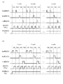
図5(a)は、本実施形態に係るガス供給シーケンスを示すタイミング図であり、図15は、本実施形態に係るGe膜の成膜メカニズムを示す図である。
Below, the film-forming sequence of this embodiment is demonstrated concretely. Here,
Supplying a Ge source gas having a structure in which Ge as a predetermined element and a ligand bonded to the Ge are arranged on the same plane as the source gas to the
Supplying NH 3 gas as a reaction gas for accelerating the decomposition of the Ge source gas to the
An example in which a germanium film (Ge film) is formed on the
FIG. 5A is a timing diagram showing a gas supply sequence according to this embodiment, and FIG. 15 is a diagram showing a film formation mechanism of a Ge film according to this embodiment.
なお、本明細書において「ウエハ」という言葉を用いた場合は、「ウエハそのもの」を意味する場合や、「ウエハとその表面に形成された所定の層や膜等との積層体(集合体)」を意味する場合(すなわち、表面に形成された所定の層や膜等を含めてウエハと称する場合)がある。また、本明細書において「ウエハの表面」という言葉を用いた場合は、「ウエハそのものの表面(露出面)」を意味する場合や、「ウエハ上に形成された所定の層や膜等の表面、すなわち、積層体としてのウエハの最表面」を意味する場合がある。 In this specification, when the term “wafer” is used, it means “wafer itself” or “a laminate (aggregate) of a wafer and a predetermined layer or film formed on the surface thereof”. "(That is, a wafer including a predetermined layer or film formed on the surface). In addition, when the term “wafer surface” is used in this specification, it means “the surface of the wafer itself (exposed surface)” or “the surface of a predetermined layer or film formed on the wafer”. That is, it may mean “the outermost surface of the wafer as a laminated body”.
従って、本明細書において「ウエハに対して所定のガスを供給する」と記載した場合は、「ウエハそのものの表面(露出面)に対して所定のガスを直接供給する」ことを意味する場合や、「ウエハ上に形成されている層や膜等に対して、すなわち、積層体としてのウエハの最表面に対して所定のガスを供給する」ことを意味する場合がある。また、本明細書において「ウエハ上に所定の層(又は膜)を形成する」と記載した場合は、「ウエハそのものの表面(露出面)上に所定の層(又は膜)を直接形成する」ことを意味する場合や、「ウエハ上に形成されている層や膜等の上、すなわち、積層体としてのウエハの最表面の上に所定の層(又は膜)を形成する」ことを意味する場合がある。 Therefore, in the present specification, the phrase “supplying a predetermined gas to the wafer” means “supplying a predetermined gas directly to the surface (exposed surface) of the wafer itself”. , It may mean that “a predetermined gas is supplied to a layer, a film, or the like formed on the wafer, that is, to the outermost surface of the wafer as a laminated body”. Further, in this specification, when “describe a predetermined layer (or film) on the wafer” is described, “determine a predetermined layer (or film) directly on the surface (exposed surface) of the wafer itself”. This means that a predetermined layer (or film) is formed on a layer or film formed on the wafer, that is, on the outermost surface of the wafer as a laminate. There is a case.
なお、本明細書において「基板」という言葉を用いた場合も、「ウエハ」という言葉を用いた場合と同様であり、その場合、上記説明において、「ウエハ」を「基板」に置き換えて考えればよい。 Note that the term “substrate” in this specification is the same as the term “wafer”. In that case, in the above description, “wafer” is replaced with “substrate”. Good.
〔基板搬入工程、基板載置工程〕
昇降機構207bを作動させ、支持台203を、図3に示すウエハ搬送位置まで下降させる。そして、ゲートバルブ44を開き、処理室201と負圧移載室11とを連通させる。そして、上述のように負圧移載機13により負圧移載室11内から処理室201内へウエハ200を搬送アーム13aで支持した状態でロードする。処理室201内に搬入されたウエハ200は、支持台203の上面から突出しているリフトピン208b上に一時的に載置される。負圧移載機13の搬送アーム13aが処理室201内から負圧移載室11内へ戻ると、ゲートバルブ44が閉じられる。
[Substrate loading process, substrate placement process]
The
続いて、昇降機構207bを作動させ、支持台203を、図2に示すウエハ処理位置まで上昇させる。その結果、リフトピン208bは支持台203の上面から埋没し、ウエハ200は、支持台203上面のサセプタ217上に載置される。
Subsequently, the
〔圧力調整工程、温度調整工程〕
続いて、処理室201内の圧力が所定の処理圧力(真空度)となるように真空ポンプ264によって真空排気される。この際、処理室201内の圧力は圧力センサ265で測定され、この測定された圧力情報に基づきAPCバルブ262がフィードバック制御される(圧力調整)。なお、真空ポンプ264は、少なくともウエハ200に対する処理が終了するまでの間は常時作動させた状態を維持する。
[Pressure adjustment process, temperature adjustment process]
Subsequently, the
また、ウエハ200の表面温度が所定の処理温度となるようにヒータ206によって加熱される。この際、ウエハ200の表面が所望の温度分布となるように、温度センサ206bが検出した温度情報に基づきヒータ206への通電具合がフィードバック制御される(温度調整)。なお、ヒータ206によるウエハ200の加熱は、少なくともウエハ200に対する処理が終了するまでの間は継続して行われる。
Further, the
なお、基板搬入工程〜温度調整工程および後述する基板搬出工程においては、真空ポンプ264を作動させつつ、バルブva3,vb3,vc3,vd3を閉じ、バルブve1,ve2,ve3,vf1,vf2,vf3を開くことで、処理室201内にN2ガスを常に流しておく。これにより、ウエハ200上へのパーティクルの付着を抑制することが可能となる。
In the substrate loading process to the temperature adjusting process and the substrate unloading process described later, while the
また、基板搬入工程〜温度調整工程と並行して、第1の液体原料(Ge原料)を気化させた第1の原料ガス(Ge原料ガス)、すなわち、所定元素としてのGeと、該Geに結合するリガンドと、が同一平面上に配置されてなる構造を有する原料ガスを生成(予備気化)させておく。すなわち、バルブva1,va2,va5を開き、キャリアガス供給管237aからMFC222aで流量制御されたキャリアガスをバブラ220a内に供給することにより、バブラ220a内部に収容された原料をバブリングにより気化させてGe原料ガスを生成させておく(Ge原料の予備気化)。
Further, in parallel with the substrate carry-in process to the temperature adjustment process, the first source gas (Ge source gas) obtained by vaporizing the first liquid source (Ge source), that is, Ge as a predetermined element and the Ge A source gas having a structure in which a ligand to be bound is arranged on the same plane is generated (preliminary vaporization). That is, by opening the valves va1, va2, va5 and supplying the carrier gas whose flow rate is controlled by the
この予備気化工程では、真空ポンプ264を作動させつつ、バルブva3を閉じたまま、バルブva4を開くことにより、Ge原料ガスを処理室201内に供給することなく処理室201をバイパスして排気しておく。バブラ220aにてGe原料ガスを安定して生成させるには所定の時間を要する。このため、本実施形態では、Ge原料ガスを予め生成させておき、バルブva3,va4の開閉を切り替えることにより、Ge原料ガスの流路を切り替える。その結果、バルブの切り替えにより、処理室201内へのGe原料ガスの安定した供給を迅速に開始あるいは停止できるようになり、好ましい。
In this preliminary vaporization step, while the
〔成膜工程〕
その後、次の2つのステップ、すなわち、ステップ1a,2aを順次実行する。
[Film formation process]
Thereafter, the next two steps, that is, steps 1a and 2a are sequentially executed.
[ステップ1a]
(Ge原料ガス供給)
バルブva4を閉じ、va3を開いて、処理室201内へのGe原料ガスの供給を開始する。原料ガス供給口210aからシャワーヘッド240の上部へと供給されたGe原料ガスは、第1バッファ空間(分散室)240cを経て分散板240aの複数の通気孔から第2バッファ空間240dへと入り、さらにシャワー板240bの複数の通気孔を通過して処理室201内に供給され、加熱されたウエハ200に対して供給される。なお、処理室201内へのGe原料ガスの供給時には、処理室201内におけるGe原料ガスの拡散を促すように、バルブve1,ve2,ve3,vf1,vf2,vf3は開いたままとし、処理室201内にN2ガスを常に流しておくことが好ましい。
[Step 1a]
(Ge source gas supply)
The valve va4 is closed and va3 is opened, and the supply of the Ge source gas into the
加熱されたウエハ200に対してGe原料ガスを供給することにより、Ge原料ガスの少なくとも一部が熱分解(自己分解)する。そして、Ge原料ガスに含まれるゲルマニウム(Ge)がウエハ200上に吸着、堆積することで、ウエハ200(最表面の下地膜)上に、例えば1原子層未満から数原子層程度の厚さのゲルマニウム層(Ge層)が形成される。
By supplying the Ge source gas to the
なお、本実施形態では、Ge原料ガスとして、Geと、該Geに結合するリガンド(R)と、が同一平面上に配置されてなる構造を有するガスを用いることとしている。これにより、ウエハ200上に形成するGe層の平坦性、すなわち、後述するGe膜の平坦性を向上させることができるようになる。以下に、この理由について図15を参照しながら説明する。図15は、その組成式中(1分子中)におけるリガンド(R)の数が3であり、Geと、該Geと結合する3つのリガンド(R)と、が同一平面上に配置されてなる構造を有するGe原料ガスを用いた場合におけるGe膜の成膜メカニズムを示す図であり、ウエハ200表面を斜め上方から見下ろした図である。
In the present embodiment, as the Ge source gas, a gas having a structure in which Ge and a ligand (R) bonded to the Ge are arranged on the same plane is used. Thereby, the flatness of the Ge layer formed on the
上述したように、加熱されたウエハ200に対してGe原料ガスを供給すると、Ge原料ガスの少なくとも一部が熱分解する。すなわち、図15(a)に示されているように、Ge原料ガスに含まれるGeと、該Geと結合していたリガンド(R)の少なくとも一部と、の結合が切れ、その少なくとも一部のリガンド(R)が、Geから分離することとなる。そして、ウエハ200上には、少なくとも一部のリガンド(R)が分離することで未結合手(ダングリングボンド)を有することとなったGeが、吸着、堆積することとなる。そして、図15(b)に示されているように、この未結合手を有することとなったGeのリガンド(R)が分離した位置に、他のGe、すなわち、ステップ1aで供給されたGe含有ガスに含まれ、リガンド(R)が分離することで未結合手を有することとなったGeが結合する(Ge−Ge結合が形成される)こととなる。上述したように、本実施形態で用いるGe原料ガスは、Geと、該Geに結合するリガンド(R)と、が同一平面上に配置されてなる平面構造を有している。従って、Geのリガンド(R)が分離した位置に、新たにやってきた他のGeが、Ge原料ガスが有していた上述の平面構造を維持しながら結合することで、Ge−Ge結合の形成は、主として平面方向、すなわち、ウエハ200の表面に平行な方向に進行していくこととなる。そして、この平面方向へのGe−Ge結合の形成が繰り返し行われることで、図15(c)に示されているように、ウエハ200上には、凹凸が少なく、平坦性の高いGe層が形成されることとなる。すなわち、ウエハ200上に形成される後述するGe膜の平坦性が向上することとなる。
As described above, when the Ge source gas is supplied to the
参考までに、Ge原料ガスとして、その組成式中(1分子中)におけるリガンド(R)の数が4であるガス、つまり、Geと、該Geに結合するリガンド(R)と、が立体的に配置されてなる立体構造を有するガスを用いた場合のGe膜の成膜メカニズムを図16に示す。図16は、ウエハ表面を斜め上方から見下ろした図である。図16(a)は、Geと少なくとも一部のリガンド(R)との結合が切れ、その少なくとも一部のリガンド(R)がGeから分離する様子を、図16(b)は、Geのリガンド(R)が分離した位置に新たにGeが結合した様子を、図16(c)は、これらを繰り返すことで立体方向にもGe−Ge結合の形成が進行する様子を示している。図16に示されているように、Ge原料ガスとして、Geと、該Geに結合するリガンド(R)と、が立体的に配置されてなる立体構造を有するガスを用いた場合、ウエハ200上でのGe−Ge結合の形成は、平面方向だけでなく、立体方向にも進行することとなる。そのため、ウエハ200上には、凹凸が大きく、平坦性の低いGe層が形成され易くなる。すなわち、ウエハ200上に形成するGe膜の平坦性が低下し易くなる。
For reference, as a Ge source gas, a gas in which the number of ligands (R) in the composition formula (in one molecule) is 4, that is, Ge and a ligand (R) bonded to the Ge are three-dimensional. FIG. 16 shows a film formation mechanism of the Ge film in the case of using a gas having a three-dimensional structure arranged on the surface. FIG. 16 is a view of the wafer surface as viewed from obliquely above. FIG. 16 (a) shows a state in which the bond between Ge and at least a portion of the ligand (R) is broken, and at least a portion of the ligand (R) is separated from Ge. FIG. FIG. 16C shows a state where Ge is newly bonded at the position where (R) is separated, and FIG. 16C shows a state where Ge—Ge bonds are formed in the three-dimensional direction by repeating these steps. As shown in FIG. 16, when a gas having a three-dimensional structure in which Ge and a ligand (R) bonded to Ge are three-dimensionally arranged is used as the Ge source gas, The formation of the Ge—Ge bond at this point proceeds not only in the planar direction but also in the three-dimensional direction. Therefore, a Ge layer having large irregularities and low flatness is easily formed on the
なお、ステップ1aで形成されるGe層中には、Geと分離することなく結合状態を維持しているリガンドが含まれる場合もある。すなわち、Ge層を構成するGeは、リガンドとの結合が完全に切れているものの他、少なくとも一部のリガンドとの結合が切れていないものも含む。このGe層中に含まれる残留リガンドは、後述するステップ2aを行うことでGe層から除去することができる。 The Ge layer formed in Step 1a may contain a ligand that maintains a bonded state without being separated from Ge. That is, the Ge constituting the Ge layer includes those in which the bond with the ligand is completely broken, and those in which the bond with at least a part of the ligand is not broken. The residual ligand contained in the Ge layer can be removed from the Ge layer by performing Step 2a described later.
但し、ウエハ200上に形成されるGe層の厚さが数原子層を超えると、後述するステップ2aでのGe層からの残留リガンドの除去作用がGe層の全体に届きにくくなる。また、ウエハ200上に形成可能なGe層の厚さの最小値は1原子層未満である。よって、Ge層の厚さは1原子層未満から数原子層程度とするのが好ましい。なお、1原子層未満の厚さの層とは不連続に形成される原子層のことを意味しており、1原子層の厚さの層とは連続的に形成される原子層のことを意味している。
However, when the thickness of the Ge layer formed on the
なお、Ge層の厚さを1原子層以下、すなわち、1原子層または1原子層未満とすることで、後述するステップ2aでのGe層からの残留リガンドの除去作用を相対的に高めることができ、ステップ2aに要する時間を短縮することができる。ステップ1aのGe層形成に要する時間を短縮することもできる。結果として、1サイクルあたりの処理時間を短縮することができ、トータルでの処理時間を短縮することも可能となる。すなわち、成膜レートを高くすることも可能となる。また、Ge層の厚さを1原子層以下とすることで、膜厚均一性の制御性を高めることも可能となる。 Note that, by setting the thickness of the Ge layer to 1 atomic layer or less, that is, 1 atomic layer or less than 1 atomic layer, the action of removing the residual ligand from the Ge layer in Step 2a described later can be relatively enhanced. And the time required for step 2a can be shortened. The time required for forming the Ge layer in step 1a can also be shortened. As a result, the processing time per cycle can be shortened, and the total processing time can be shortened. That is, the film forming rate can be increased. In addition, by controlling the thickness of the Ge layer to 1 atomic layer or less, it becomes possible to improve the controllability of film thickness uniformity.
(残留ガス除去)
所定の厚さのGe層が形成された後、バルブva3を閉じ、バルブva4を開いて、処理室201内へのGe原料ガスの供給を停止する。このとき、排気管261のAPCバルブ262は開いたままとして、真空ポンプ264により処理室201内を真空排気し、処理室201内に残留する未反応もしくはGe層形成に寄与した後のGe原料ガスを処理室201内から排除する。なお、このとき、バルブve1,ve2,ve3,vf1,vf2,vf3は開いたままとして、不活性ガスとしてのN2ガスの処理室201内への供給を維持する。N2ガスはパージガスとして作用し、これにより、処理室201内に残留する未反応もしくはGe層形成に寄与した後のGe原料ガスを処理室201内から排除する効果を高めることができる。
(Residual gas removal)
After the Ge layer having a predetermined thickness is formed, the valve va3 is closed and the valve va4 is opened, and the supply of the Ge source gas into the
なお、このとき、処理室201内に残留するガスを完全に排除しなくてもよく、処理室201内を完全にパージしなくてもよい。処理室201内に残留するガスが微量であれば、その後に行われるステップ2aにおいて悪影響が生じることはない。このとき処理室201内に供給するN2ガスの流量も大流量とする必要はなく、例えば、処理容器202(処理室201)の容積と同程度の量を供給することで、ステップ2aにおいて悪影響が生じない程度のパージを行うことができる。このように、処理室201内を完全にパージしないことで、パージ時間を短縮し、スループットを向上させることができる。また、N2ガスの消費も必要最小限に抑えることが可能となる。
At this time, the gas remaining in the
Ge原料ガスとしては、上述したように、Geと、該Geに結合するリガンドと、が同一平面上に配置されてなる構造を有するガスを用いることが好ましい。なお、Geに結合するリガンドの数は、3以下であることが好ましく、2以下であることがより好ましい。言い換えれば、Geの原子価は4であるため、Geとリガンドとの結合が二重結合、または三重結合、もしくはそれ以上の結合を含むようなガスを用いることが好ましい。不活性ガスとしては、N2ガスの他、Arガス、Heガス、Neガス、Xeガス等の希ガスを用いてもよい。 As the Ge source gas, as described above, it is preferable to use a gas having a structure in which Ge and a ligand bonded to Ge are arranged on the same plane. Note that the number of ligands bonded to Ge is preferably 3 or less, and more preferably 2 or less. In other words, since the valence of Ge is 4, it is preferable to use a gas in which the bond between Ge and the ligand includes a double bond, a triple bond, or a higher bond. As the inert gas, a rare gas such as Ar gas, He gas, Ne gas, or Xe gas may be used in addition to N 2 gas.
[ステップ2a]
(NH3ガス供給)
ステップ1aが終了し処理室201内の残留ガスを除去した後、バルブvd1,vd2,vd3を開いて、処理室201内へのNH3ガスの供給を開始する。反応ガス供給口210bから供給されたNH3ガスは、シャワー板240bの下方側から、つまり、シャワーヘッド240を介さずに処理室201内に供給され、加熱されたウエハ200に対して供給される。なお、処理室201内へのNH3ガスの供給時には、処理室201内におけるNH3ガスの拡散を促すように、バルブve1,ve2,ve3,vf1,vf2,vf3は開いたままとし、処理室201内にN2ガスを常に流しておくことが好ましい。
[Step 2a]
(NH 3 gas supply)
After step 1a is completed and residual gas in the
加熱されたウエハ200に対してNH3ガスを供給することにより、ステップ1aで形成されたGe層に含まれるGe原料やその成分の分解が促されることとなる。すなわち、NH3ガスの触媒作用により、Ge層に含まれている残留リガンド、つまり、ステップ1aでGeと分離することなく結合状態を維持する等してGe層に含まれることとなっていた残留リガンドの、Ge層を構成するGeからの分離が促されることとなる。
By supplying NH 3 gas to the
Ge層を構成するGeは、残留リガンドが分離することで未結合手(ダングリングボンド)を新たに有することとなる。そして、この未結合手には、新たにやってくるGe、すなわち、次のステップ1aで供給されるGe原料ガスに含まれ、リガンドが分離することで未結合手を有することとなったGeが結合することとなる。すなわち、ステップ2aを実施することで、ウエハ200上でのGe−Ge結合の形成を促すことができ、ウエハ200上へのGe層の形成、すなわち、後述するGe膜の形成を促進することができるようになる。なお、Geのリガンドが分離した位置に、新たにやってきた他のGeが結合することで、凹凸が少なく、平坦性の高いGe層、すなわち、平坦性の高いGe膜を形成できる点は、上述した通りである。
Ge constituting the Ge layer newly has dangling bonds (dangling bonds) due to separation of residual ligands. And, this unbonded hand is bonded to newly coming Ge, that is, Ge contained in the Ge source gas supplied in the next step 1a and having the unbonded hand by separating the ligand. It will be. That is, by performing Step 2a, formation of a Ge—Ge bond on the
また、Ge層を構成するGeから残留リガンドを分離させることで、Ge層を、炭素(C)、水素(H)、酸素(O)および窒素(N)等の不純物の少ない層に改質させることができるようになる。つまり、Ge層から残留リガンドを除去することで、後述するGe膜中におけるC、H、OおよびN等の不純物濃度を低減させることができるようになる。 Further, by separating the residual ligand from Ge constituting the Ge layer, the Ge layer is modified into a layer having few impurities such as carbon (C), hydrogen (H), oxygen (O), and nitrogen (N). Will be able to. That is, by removing the residual ligand from the Ge layer, the concentration of impurities such as C, H, O, and N in the Ge film described later can be reduced.
また、ステップ1aで形成したGe層に対してNH3ガスを供給することにより、Ge層、すなわち、Ge膜を構成する結晶粒の粒径を小さくすることができるようになる。これにより、凹凸がより少なく、平坦性のより高いGe膜を形成できるようになる。 Further, by supplying NH 3 gas to the Ge layer formed in step 1a, the grain size of the crystal grains constituting the Ge layer, that is, the Ge film can be reduced. As a result, a Ge film with less unevenness and higher flatness can be formed.
(残留ガス除去)
Ge層から残留リガンドを除去した後、バルブvd3を閉じ、処理室201内へのNH3ガスの供給を停止する。このとき、排気管261のAPCバルブ262は開いたままとして、真空ポンプ264により処理室201内を真空排気し、処理室201内に残留する未反応もしくはGe層からの残留リガンドの除去に寄与した後のNH3ガスや反応副生成物を処理室201内から排除する。なお、このとき、バルブve1,ve2,ve3,vf1,vf2,vf3は開いたままとして、不活性ガスとしてのN2ガスの処理室201内への供給を維持する。N2ガスはパージガスとして作用し、これにより、処理室201内に残留する未反応もしくはGe層からの残留リガンドの除去に寄与した後のNH3ガスや反応副生成物を処理室201内から排除する効果を高めることができる。
(Residual gas removal)
After the residual ligand is removed from the Ge layer, the valve vd3 is closed, and the supply of NH 3 gas into the
なお、このとき、処理室201内に残留するガスを完全に排除しなくてもよく、処理室201内を完全にパージしなくてもよい。処理室201内に残留するガスが微量であれば、その後に行われるステップ1aにおいて悪影響が生じることはない。このとき処理室201内に供給するN2ガスの流量も大流量とする必要はなく、例えば、処理容器202(処理室201)の容積と同程度の量を供給することで、ステップ1aにおいて悪影響が生じない程度のパージを行うことができる。このように、処理室201内を完全にパージしないことで、パージ時間を短縮し、スループットを向上させることができる。また、N2ガスの消費も必要最小限に抑えることが可能となる。
At this time, the gas remaining in the
なお、反応ガスとしては、アンモニア(NH3)ガスの他、例えば、ヒドラジン(N2H4)ガス、ジアゼン(N2H2)ガス、N3H8ガス、水素(H2)ガス等の還元ガス、すなわち、水素含有ガスを用いてもよい。また、不活性ガスとしては、N2ガスの他、Arガス、Heガス、Neガス、Xeガス等の希ガスを用いてもよい。 In addition to ammonia (NH 3 ) gas, examples of the reactive gas include hydrazine (N 2 H 4 ) gas, diazene (N 2 H 2 ) gas, N 3 H 8 gas, and hydrogen (H 2 ) gas. A reducing gas, that is, a hydrogen-containing gas may be used. Further, as the inert gas, a rare gas such as Ar gas, He gas, Ne gas, Xe gas, etc. may be used in addition to N 2 gas.
[所定回数実施]
上述したステップ1a,2aを1サイクルとして、このサイクルを1回以上(所定回数)行うことにより、ウエハ200上に、所定膜厚のGeを含む膜(Ge膜)が形成される。なお、上述のサイクルは、複数回繰り返すのが好ましい。すなわち、1サイクルあたりに形成するGe層の厚さを所望の膜厚よりも小さくして、上述のサイクルを所望の膜厚になるまで複数回繰り返すのが好ましい。
[Perform a specified number of times]
Steps 1a and 2a described above are set as one cycle, and this cycle is performed once or more (a predetermined number of times), thereby forming a film (Ge film) containing Ge with a predetermined film thickness on the
なお、サイクルを複数回行う場合、少なくとも2サイクル目以降の各ステップにおいて、「ウエハ200に対して所定のガスを供給する」と記載した部分は、「ウエハ200上に形成されている層に対して、すなわち、積層体としてのウエハ200の最表面に対して所定のガスを供給する」ことを意味し、「ウエハ200上に所定の層を形成する」と記載した部分は、「ウエハ200上に形成されている層の上、すなわち、積層体としてのウエハ200の最表面の上に所定の層を形成する」ことを意味している。この点は、上述の通りである。なお、この点は、後述する各変形例、他の実施形態においても同様である。
In the case where the cycle is performed a plurality of times, at least in each step after the second cycle, the portion described as “suppliing a predetermined gas to the
本実施形態における成膜工程でのウエハ200の処理条件としては、
ウエハ温度:200〜400℃
処理室内圧力:50〜400Pa
Ge原料ガス流量:0.1〜100sccm
NH3ガス流量:50〜1000sccm
N2流量:0〜2000sccm
Ge原料ガス供給時間:1〜120秒、好ましくは1〜60秒
NH3ガス供給時間:1〜120秒、好ましくは1〜60秒
N2ガス供給時間(パージ時間):1〜120秒、好ましくは1〜60秒
Ge膜厚:1〜100nm
が例示される。
As processing conditions of the
Wafer temperature: 200-400 ° C
Processing chamber pressure: 50 to 400 Pa
Ge source gas flow rate: 0.1 to 100 sccm
NH 3 gas flow rate: 50-1000 sccm
N 2 flow rate: 0 to 2000 sccm
Ge source gas supply time: 1-120 seconds, preferably 1-60 seconds NH 3 gas supply time: 1-120 seconds, preferably 1-60 seconds N 2 gas supply time (purge time): 1-120 seconds, preferably 1-60 seconds Ge film thickness: 1-100 nm
Is exemplified.
〔パージ及び大気圧復帰工程〕
所定膜厚のGe膜が形成された後、排気管261のAPCバルブ262は開いたままとして、真空ポンプ264により処理室201内を真空排気し、処理室201内に残留するガスや反応副生成物を処理室201内から排除する(残留ガス除去)。なお、このとき、バルブve1,ve2,ve3,vf1,vf2,vf3は開いたままとして、不活性ガスとしてのN2ガスの処理室201内への供給を維持する。N2ガスはパージガスとして作用し、これにより、処理室201内に残留するガスや反応副生成物を処理室201内から排除する効果を高めることができる。
[Purge and atmospheric pressure recovery process]
After the Ge film having a predetermined thickness is formed, the
〔基板搬出工程〕
その後、上述した基板搬入工程、基板載置工程に示した手順とは逆の手順により、Ge膜を形成した後のウエハ200を、処理室201内から負圧移載室11内へ搬出する。その後、ウエハ200の温度が室温になるまで、負圧移載室11に隣接する保持室内で処理後のウエハ200を保持する。なお、形成したGe膜の酸化を抑制するように、負圧移載室11内や保持室内の雰囲気は、例えば、大気圧未満の圧力雰囲気であって、かつ、N2ガス等の不活性ガス雰囲気とし、酸素(O2)ガスの分圧を低下させておく。
[Substrate unloading process]
Thereafter, the
(3)本実施形態に係る効果
本実施形態によれば、以下に示す効果のうち1つ又は複数の効果を奏する。
(3) Effects according to this embodiment According to this embodiment, one or more of the following effects are achieved.
本実施形態によれば、ステップ1aで用いるGe原料ガスとして、Geと、該Geに結合するリガンド(R)と、が同一平面上に配置されてなる平面構造を有するガスを用いることとしている。そして、Ge原料ガスの熱分解によりGeのリガンドが分離した位置に、新たにやってきたGeが、Ge原料ガスが有していた平面構造を維持しながら結合することで、Ge−Ge結合の形成を、平面方向に進行させることができる。これにより、ウエハ200上に形成するGe層の平坦性、すなわち、Ge膜の平坦性を向上させることができるようになる。
According to this embodiment, as the Ge source gas used in step 1a, a gas having a planar structure in which Ge and a ligand (R) bonded to Ge are arranged on the same plane is used. Then, Ge that newly arrives at the position where the Ge ligand is separated by thermal decomposition of the Ge source gas, while maintaining the planar structure of the Ge source gas, thereby forming a Ge—Ge bond. Can be advanced in the plane direction. Thereby, the flatness of the Ge layer formed on the
また、本実施形態によれば、ステップ1aでGe層を形成した後、加熱されたウエハ200に対してGe原料ガスの分解を促すNH3ガスを供給するステップ2aを実施するようにしている。そして、NH3ガスの触媒作用により、Ge層に含まれている残留リガンドのGeからの分離を促進させるようにしている。その結果、Ge層を構成するGeが新たな未結合手を有することとなり、この未結合手に、新たにやってくるGeが結合することで、ウエハ200上へのGe層の形成、すなわち、Ge膜の形成が促進されるようになる。
Further, according to the present embodiment, after the Ge layer is formed in Step 1a, Step 2a for supplying NH 3 gas that promotes decomposition of Ge source gas to the
また、本実施形態によれば、NH3ガスの触媒作用により、Ge層を構成するGeから残留リガンドを分離させることで、Ge層中の不純物濃度、すなわち、Ge膜中におけるC、H、OおよびN等の不純物濃度を低減させることができるようになる。 In addition, according to the present embodiment, the residual ligand is separated from Ge constituting the Ge layer by the catalytic action of NH 3 gas, so that the impurity concentration in the Ge layer, that is, C, H, O in the Ge film is obtained. In addition, the concentration of impurities such as N and N can be reduced.
また、本実施形態によれば、ステップ1aで形成したGe層に対してNH3ガスを供給するステップ2aを実施することにより、Ge層、すなわち、Ge膜を構成する結晶粒の粒径を小さくすることができるようになる。これにより、凹凸がより少なく、平坦性のより高いGe膜を形成できるようになる。 In addition, according to the present embodiment, by performing Step 2a in which NH 3 gas is supplied to the Ge layer formed in Step 1a, the grain size of the crystal grains constituting the Ge layer, that is, the Ge film is reduced. Will be able to. As a result, a Ge film with less unevenness and higher flatness can be formed.
(変形例)
図5(a)に示した上述の成膜シーケンスでは、Ge原料ガス供給工程とNH3ガス供給工程とを、それらの間に処理室201内をパージする残留ガス除去工程を挟んで交互に行うサイクルを所定回数行う例について説明したが、本実施形態は係る形態に限定されない。すなわち、図5(b)に示されているように、Ge原料ガス供給工程とNH3ガス供給工程とを、それらの間に処理室201内をパージする残留ガス除去工程を挟まずに交互に連続して行うサイクルを所定回数(n回)行うようにしてもよい。但し、図5(a)に示す成膜シーケンスの方が、処理室201内においてGe原料ガスとNH3ガスとが気相中で混合し反応してしまうことをより確実に防ぐことができ、処理室201内でのパーティクルの発生を抑制したり、処理室201内のクリーニング頻度を低減したりすることができ、好ましい。
(Modification)
In the above-described film forming sequence shown in FIG. 5A, the Ge source gas supply process and the NH 3 gas supply process are alternately performed with a residual gas removal process for purging the inside of the
<本発明の第2実施形態>
上述の実施形態では、1元系の膜であるGe膜を基板上に形成する例について説明したが、本発明は係る形態に限定されない。すなわち、複数種類の所定元素を含む膜、すなわち、多元系の膜を基板上に形成する場合にも、本発明は好適に適用可能である。
<Second Embodiment of the Present Invention>
In the above-described embodiment, the example in which the Ge film, which is a single-system film, is formed on the substrate has been described. However, the present invention is not limited to such a form. That is, the present invention can be suitably applied to the case where a film containing a plurality of types of predetermined elements, that is, a multi-element film is formed on a substrate.
以下に、本発明の第2実施形態について説明する。なお、ここでは、
処理室201内のウエハ200に対して、所定元素としてのGeと、該Geに結合するリガンドと、が同一平面上に配置されてなる構造を有するGe原料ガスと、所定元素としてのSbと、該Sbに結合するリガンドと、が同一平面上に配置されてなる構造を有するSb原料ガスと、所定元素としてのTeと、該Teに結合するリガンドと、が同一平面上に配置されてなる構造を有するTe原料ガスと、を供給する工程と、
処理室201内のウエハ200に対して、Ge原料ガス、Sb原料ガスおよびTe原料ガスの分解をそれぞれ促進させる反応ガスとしてNH3ガスを供給する工程と、
を交互に所定回数(1回以上)行うことで、ウエハ200上に、Ge,Sb,Teの3つの所定元素を含む3元系の膜であるGeSbTe膜を形成する例について説明する。
図6(a)は、本実施形態に係るガス供給シーケンスを示すタイミング図である。なお、以下では、Ge原料ガス、Sb原料ガス、Te原料ガスを総称して、単に、原料ガスとも称する。
The second embodiment of the present invention will be described below. Here,
Ge source gas having a structure in which Ge as a predetermined element and a ligand bonded to Ge are arranged on the same plane with respect to the
Supplying NH 3 gas as a reaction gas for accelerating the decomposition of the Ge source gas, the Sb source gas, and the Te source gas with respect to the
An example of forming a GeSbTe film, which is a ternary film containing three predetermined elements of Ge, Sb, and Te, on the
FIG. 6A is a timing chart showing a gas supply sequence according to the present embodiment. Hereinafter, the Ge raw material gas, the Sb raw material gas, and the Te raw material gas are collectively referred to simply as a raw material gas.
〔基板搬入工程、載置工程〜圧力調整工程、温度調整工程〕
基板搬入工程、載置工程〜圧力調整工程、温度調整工程については、上述の第1実施形態と同様の処理手順および同様の処理条件で行う。
[Substrate carry-in process, placement process-pressure adjustment process, temperature adjustment process]
About a board | substrate carrying-in process, a mounting process-a pressure adjustment process, and a temperature adjustment process, it carries out on the same process sequence and the same process conditions as the above-mentioned 1st Embodiment.
なお、Ge原料の予備気化工程と並行して、第2の液体原料(Sb原料)を気化させた第2の原料ガス(Sb原料ガス)、すなわち、所定元素としてのSbと、該Sbに結合するリガンドと、が同一平面上に配置されてなる構造を有する原料ガスを生成(予備気化)させておく。すなわち、バルブvb1,vb2,vb5を開き、キャリアガス供給管237bからMFC222bで流量制御されたキャリアガスをバブラ220b内に供給することにより、バブラ220b内部に収容された原料をバブリングにより気化させてSb原料ガスを生成させておく(Sb原料の予備気化)。
In parallel with the Ge raw material pre-vaporization step, a second raw material gas (Sb raw material gas) obtained by vaporizing the second liquid raw material (Sb raw material), that is, Sb as a predetermined element and bonded to Sb. A raw material gas having a structure in which a ligand to be arranged on the same plane is generated (preliminary vaporization). That is, by opening the valves vb1, vb2, and vb5 and supplying the carrier gas whose flow rate is controlled by the
また、上記と並行して、第3の液体原料(Te原料)を気化させた第3の原料ガス(Te原料ガス)、すなわち、所定元素としてのTeと、このTeに結合するリガンドと、が同一平面上に配置されてなる構造を有する原料ガスを生成(予備気化)させておく。すなわち、バルブvc1,vc2,vc5を開き、キャリアガス供給管237cからMFC222cで流量制御されたキャリアガスをバブラ220c内に供給することにより、バブラ220c内部に収容された原料をバブリングにより気化させてTe原料ガスを生成させておく(Te原料の予備気化)。
In parallel with the above, a third raw material gas (Te raw material gas) obtained by vaporizing the third liquid raw material (Te raw material), that is, Te as a predetermined element and a ligand that binds to this Te, A raw material gas having a structure arranged on the same plane is generated (preliminarily vaporized). That is, by opening the valves vc1, vc2, and vc5 and supplying the carrier gas whose flow rate is controlled by the MFC 222c from the carrier
これらの予備気化工程では、真空ポンプ264を作動させつつ、バルブva3,vb3,vc3を閉じたまま、バルブva4,vb4,vc4を開くことにより、原料ガスを処理室201内に供給することなく処理室201をバイパスして排気しておく。バブラ220a,220b,220cにて原料ガスを安定して生成させるには所定の時間を要する。このため、本実施形態では、原料ガスを予め生成させておき、バルブva3,vb3,vc3と、バルブva4,vb4,vc4との開閉を切り替えることにより、原料ガスの流路を切り替える。その結果、バルブの切り替えにより、処理室201内への原料ガスの安定した供給を迅速に開始あるいは停止できるようになり、好ましい。
In these preliminary vaporization steps, while the
〔成膜工程〕
その後、次の2つのステップ、すなわち、ステップ1b,2bを順次実行する。
[Film formation process]
Thereafter, the next two steps, that is, steps 1b and 2b are sequentially executed.
[ステップ1b]
(原料ガス供給)
va4,vb4,vc4を同時に閉じ、va3,vb3,vc3を同時に開いて、処理室201内へのGe原料ガス、Sb原料ガス、Te原料ガスの供給を同時に開始する。原料ガス供給口210aからシャワーヘッド240の上部へと供給されたGe原料ガス、Sb原料ガス、Te原料ガスは、それぞれ、第1バッファ空間(分散室)240cを経て分散板240aの複数の通気孔から第2バッファ空間240dへと入り、さらにシャワー板240bの複数の通気孔を通過して処理室201内に供給され、加熱されたウエハ200に対して供給される。なお、処理室201内へのGe原料ガス、Sb原料ガス、Te原料ガスの供給時には、処理室201内におけるGe原料ガス、Sb原料ガス、Te原料ガスの拡散を促すように、バルブve1,ve2,ve3,vf1,vf2,vf3は開いたままとし、処理室201内にN2ガスを常に流しておくことが好ましい。
[Step 1b]
(Raw material gas supply)
va4, vb4, and vc4 are simultaneously closed and va3, vb3, and vc3 are simultaneously opened, and supply of the Ge source gas, Sb source gas, and Te source gas into the
加熱されたウエハ200に対してGe原料ガス、Sb原料ガス、Te原料ガスを供給することにより、Ge原料ガス、Sb原料ガス、Te原料ガスの少なくとも一部がそれぞれ熱分解(自己分解)する。そして、Ge原料ガス、Sb原料ガス、Te原料ガスに含まれるゲルマニウム(Ge)、アンチモン(Sb)、テルル(Te)がウエハ200上に吸着、堆積することで、ウエハ200(最表面の下地膜)上に、例えば1原子層未満から数原子層程度の厚さのGe,Sb,Teの3つの所定元素を含む3元系の層であるGeSbTe層が形成される。
By supplying Ge source gas, Sb source gas, and Te source gas to the
なお、本実施形態では、Ge原料ガス、Sb原料ガス、Te原料ガスとして、所定元素(Ge,Sb,Te)と、該所定元素(Ge,Sb,Te)に結合するリガンドと、が同一平面上に配置されてなる構造を有するガスをそれぞれ用いることとしている。これにより、ウエハ200上に形成するGeSbTe層の平坦性、すなわち、後述するGeSbTe膜の平坦性を向上させることができるようになる。この点は、第1実施形態で説明した通りである。
In the present embodiment, as the Ge source gas, the Sb source gas, and the Te source gas, the predetermined element (Ge, Sb, Te) and the ligand bonded to the predetermined element (Ge, Sb, Te) are in the same plane. Each of the gases having a structure arranged above is used. Thereby, the flatness of the GeSbTe layer formed on the
なお、ステップ1bで形成されるGeSbTe層中には、所定元素(Ge,Sb,Te)と分離することなく結合状態を維持しているリガンドが含まれる場合もある。すなわち、GeSbTe層を構成する所定元素(Ge,Sb,Te)は、少なくとも一部のリガンドとの結合が切れていない場合もある。このGeSbTe層中に含まれる残留リガンドは、後述するステップ2bを行うことでGeSbTe層から除去することができる。なお、後述するステップ2bでのGeSbTe層からの残留リガンドの除去作用を十分に生じさせるため、GeSbTe層の厚さを1原子層未満から数原子層程度とするのが好ましい。この点は、第1実施形態で説明した通りである。 The GeSbTe layer formed in step 1b may include a ligand that maintains a bonded state without being separated from a predetermined element (Ge, Sb, Te). That is, the predetermined elements (Ge, Sb, Te) constituting the GeSbTe layer may not be broken with at least some of the ligands. The residual ligand contained in the GeSbTe layer can be removed from the GeSbTe layer by performing Step 2b described later. It should be noted that the thickness of the GeSbTe layer is preferably set to be less than one atomic layer to several atomic layers in order to sufficiently remove the residual ligand from the GeSbTe layer in Step 2b described later. This point is as described in the first embodiment.
(残留ガス除去)
所定の厚さのGeSbTe層が形成された後、バルブva3,vb3,vc3を閉じ、バルブva4,vb4,vc4を開いて、処理室201内へのGe原料ガス、Sb原料ガス、Te原料ガスの供給を停止する。このとき、排気管261のAPCバルブ262は開いたままとして、真空ポンプ264により処理室201内を真空排気し、処理室201内に残留する未反応もしくはGeSbTe層形成に寄与した後のGe原料ガス、Sb原料ガス、Te原料ガスを処理室201内から排除する。なお、このとき、バルブve1,ve2,ve3,vf1,vf2,vf3は開いたままとして、不活性ガスとしてのN2ガスの処理室201内への供給を維持する点や、処理室201内に残留するガスを完全に排除しなくてもよく、処理室201内を完全にパージしなくてもよい。この点は、第1実施形態で説明した通りである。
(Residual gas removal)
After the GeSbTe layer having a predetermined thickness is formed, the valves va3, vb3, vc3 are closed, the valves va4, vb4, vc4 are opened, and the Ge source gas, Sb source gas, and Te source gas into the
なお、Sb原料ガスとしては、例えば、トリスジメチルアミノアンチモン(Sb[N(CH3)2]3、略称:TDMASb)ガス、トリイソプロピルアンチモン(Sb(i−C3H7)3、略称:TIPSb)ガス、トリエチルアンチモン(Sb(C2H5)3、略称:TESb)ガス、ターシャリブチルジメチルアンチモン((t−C4H9)Sb(CH3)2、略称:TBDMSb)ガス等を用いることができる。Sbの原子価は3であるため、Sbに結合するリガンドの数は常に3以下となる。すなわち、ここに例示したSb原料ガスは、Sbと、該Sbに結合するリガンドと、が同一平面上に配置されてなる構造を有し易いガスであるといえる。 Examples of the Sb source gas include trisdimethylaminoantimony (Sb [N (CH 3 ) 2 ] 3 , abbreviation: TDMASb) gas, triisopropylantimony (Sb (i-C 3 H 7 ) 3 , abbreviation: TIPSb. ) Gas, triethylantimony (Sb (C 2 H 5 ) 3 , abbreviation: TESb) gas, tertiarybutyldimethylantimony ((tC 4 H 9 ) Sb (CH 3 ) 2 , abbreviation: TBDMSb) gas, or the like is used. be able to. Since the valence of Sb is 3, the number of ligands binding to Sb is always 3 or less. That is, it can be said that the Sb source gas exemplified here is a gas that easily has a structure in which Sb and a ligand that binds to Sb are arranged on the same plane.
また、Te原料ガスとしては、例えば、ジターシャリーブチルテルル(Te(t−C4H9)2、略称:DTBTe)ガス、ジイソプロピルテルル(Te(i−C3H7)2、略称:DIPTe)ガス、ジメチルテルル(Te(CH3)2、略称:DMTe)ガス、ジエチルテルル(Te(C2H5)2、略称:DETe)ガス等を用いることができる。Teの原子価は2であるため、Teに結合するリガンドの数は常に2以下となる。すなわち、ここに例示したTe原料ガスは、Teと、該Teに結合するリガンドと、が同一平面上に配置されてなる構造を有するガスであるといえる。 Examples of the Te source gas include ditertiary butyl tellurium (Te (t-C 4 H 9 ) 2 , abbreviation: DTBTe) gas, diisopropyl tellurium (Te (i-C 3 H 7 ) 2 , abbreviation: DIPTe). Gas, dimethyl tellurium (Te (CH 3 ) 2 , abbreviation: DMTe) gas, diethyl tellurium (Te (C 2 H 5 ) 2 , abbreviation: DETe) gas, or the like can be used. Since the valence of Te is 2, the number of ligands binding to Te is always 2 or less. That is, it can be said that the Te source gas exemplified here is a gas having a structure in which Te and a ligand bonded to Te are arranged on the same plane.
[ステップ2b]
(NH3ガス供給)
ステップ2bは、第1実施形態のステップ2aと同様の処理手順および同様の処理条件で行う。すなわち、このステップでは、加熱されたウエハ200に対して、原料ガスの分解を促すNH3ガスを供給する。
[Step 2b]
(NH 3 gas supply)
Step 2b is performed with the same processing procedure and the same processing conditions as step 2a of the first embodiment. That is, in this step, NH 3 gas that promotes decomposition of the source gas is supplied to the
加熱されたウエハ200に対してNH3ガスを供給することにより、ステップ1bで形成されたGeSbTe層に含まれるGe原料、Sb原料、Te原料や、それらの成分の分解がそれぞれ促されることとなる。すなわち、NH3ガスの触媒作用により、GeSbTe層に含まれている残留リガンド、つまり、ステップ1bで所定元素(Ge,Sb,Te)と分離することなく結合状態を維持する等してGeSbTe層に含まれることとなっていた残留リガンドの、GeSbTe層を構成する所定元素(Ge,Sb,Te)からの分離がそれぞれ促されることとなる。
By supplying NH 3 gas to the
その結果、GeSbTe層を構成する所定元素(Ge,Sb,Te)がそれぞれ新たな未結合手を有することとなり、この未結合手に、新たにやってくる所定元素(Ge,Sb,Te)が結合することで、ウエハ200上へのGeSbTe層の形成、すなわち、後述するGeSbTe膜の形成が促進されるようになる。なお、所定元素(Ge,Sb,Te)のリガンドが分離した位置に、新たにやってきた他の所定元素(Ge,Sb,Te)が結合することで、凹凸が少なく、平坦性の高いGeSbTe層、すなわち、GeSbTe膜を形成できる点は、上述した通りである。
As a result, each predetermined element (Ge, Sb, Te) constituting the GeSbTe layer has a new dangling bond, and a new predetermined element (Ge, Sb, Te) is bonded to the dangling bond. As a result, formation of a GeSbTe layer on the
また、GeSbTe層を構成する所定元素(Ge,Sb,Te)から残留リガンドを分離させることで、GeSbTe層中の不純物濃度、すなわち、後述するGeSbTe膜中におけるC、H、OおよびN等の不純物濃度を低減させることができるようになる。 Further, by separating the residual ligand from the predetermined elements (Ge, Sb, Te) constituting the GeSbTe layer, the impurity concentration in the GeSbTe layer, that is, impurities such as C, H, O, and N in the GeSbTe film described later The concentration can be reduced.
(残留ガス除去)
GeSbTe層から残留リガンドを除去した後、バルブvd3を閉じ、処理室201内へのNH3ガスの供給を停止する。このとき、排気管261のAPCバルブ262は開いたままとして、真空ポンプ264により処理室201内を真空排気し、処理室201内に残留する未反応もしくはGeSbTe層からの残留リガンドの除去に寄与した後のNH3ガスや反応副生成物を処理室201内から排除する。なお、このとき、バルブve1,ve2,ve3,vf1,vf2,vf3は開いたままとして、不活性ガスとしてのN2ガスの処理室201内への供給を維持する点や、処理室201内に残留するガスを完全に排除しなくてもよく、処理室201内を完全にパージしなくてもよい点は、第1実施形態で説明した通りである。
(Residual gas removal)
After the residual ligand is removed from the GeSbTe layer, the valve vd3 is closed and the supply of NH 3 gas into the
[所定回数実施]
上述したステップ1b,2bを1サイクルとして、このサイクルを1回以上(所定回数)行うことにより、ウエハ200上に、所定膜厚のGe,Sb,Teを含む膜(GeSbTe膜)が形成される。なお、上述のサイクルは、複数回繰り返すのが好ましい。すなわち、1サイクルあたりに形成するGeSbTe層の厚さを所望の膜厚よりも小さくして、上述のサイクルを所望の膜厚になるまで複数回繰り返すのが好ましい。
[Perform a specified number of times]
By performing the above-described steps 1b and 2b as one cycle and performing this cycle one or more times (predetermined number of times), a film (GeSbTe film) containing Ge, Sb, and Te having a predetermined film thickness is formed on the
本実施形態における成膜工程でのウエハ200の処理条件としては、
ウエハ温度:200〜400℃
処理室内圧力:50〜400Pa
Ge原料ガス流量:0.1〜100sccm
Sb原料ガス流量:0.1〜100sccm
Te原料ガス流量:0.1〜100sccm
NH3ガス流量:50〜1000sccm
N2流量:0〜2000sccm
Ge原料ガス供給時間:1〜120秒、好ましくは1〜60秒
Sb原料ガス供給時間:1〜120秒、好ましくは1〜60秒
Te原料ガス供給時間:1〜120秒、好ましくは1〜60秒
NH3ガス供給時間:1〜120秒、好ましくは1〜60秒
N2ガス供給時間(パージ時間):1〜120秒、好ましくは1〜60秒
GeSbTe膜厚:1〜100nm
が例示される。
As processing conditions of the
Wafer temperature: 200-400 ° C
Processing chamber pressure: 50 to 400 Pa
Ge source gas flow rate: 0.1 to 100 sccm
Sb source gas flow rate: 0.1 to 100 sccm
Te source gas flow rate: 0.1 to 100 sccm
NH 3 gas flow rate: 50-1000 sccm
N 2 flow rate: 0 to 2000 sccm
Ge source gas supply time: 1-120 seconds, preferably 1-60 seconds Sb source gas supply time: 1-120 seconds, preferably 1-60 seconds Te source gas supply time: 1-120 seconds, preferably 1-60 Second NH 3 gas supply time: 1 to 120 seconds, preferably 1 to 60 seconds N 2 gas supply time (purge time): 1 to 120 seconds, preferably 1 to 60 seconds GeSbTe film thickness: 1 to 100 nm
Is exemplified.
〔パージ及び大気圧復帰工程〜基板搬出工程〕
パージ及び大気圧復帰工程〜基板搬出工程については、上述の第1実施形態と同様の処理手順および同様の処理条件で行う。
[Purge and atmospheric pressure recovery process-substrate unloading process]
The purge and atmospheric pressure return process to substrate carry-out process are performed under the same processing procedure and the same processing conditions as in the first embodiment.
本実施形態においても、上述の第1実施形態と同様の効果を奏する。 Also in this embodiment, there exists an effect similar to the above-mentioned 1st Embodiment.
すなわち、ステップ1bで用いるGe原料ガス、Sb原料ガス、Te原料ガスとして、所定元素(Ge,Sb,Te)と、この所定元素(Ge,Sb,Te)に結合するリガンド(R)と、が同一平面上に配置されてなる平面構造を有するガスをそれぞれ用いることで、ウエハ200上に形成するGeSbTe膜の平坦性を向上させることができるようになる。なお、Ge原料ガス、Sb原料ガス、Te原料ガスの全てのガスが上述の平面構造を有する場合に限らず、これらのガスのうち一部のガスのみが上述の平面構造をする場合であっても、GeSbTe膜の平坦性を向上させる効果が得られる。但し、Ge原料ガス、Sb原料ガス、Te原料ガスの全てのガスが上述の平面構造を有するほうが、GeSbTe膜の平坦性を向上させる効果を高めることができ、好ましい。
That is, as the Ge source gas, Sb source gas, and Te source gas used in Step 1b, a predetermined element (Ge, Sb, Te) and a ligand (R) bonded to the predetermined element (Ge, Sb, Te) are By using each gas having a planar structure arranged on the same plane, the flatness of the GeSbTe film formed on the
また、ステップ1bでGeSbTe層を形成した後、加熱されたウエハ200に対してGe原料ガス、Sb原料ガス、Te原料ガスの分解を促すNH3ガスを供給するステップ2bを実施することで、GeSbTe層から残留リガンド(R)を除去することができ、これにより、ウエハ200上へのGeSbTe膜の形成を促進することができ、また、GeSbTe膜中の不純物濃度を低減させることができるようになる。
Further, after the GeSbTe layer is formed in Step 1b, Step 2b of supplying NH 3 gas that promotes decomposition of Ge source gas, Sb source gas, and Te source gas to the
(変形例)
図6(a)に示した上述の成膜シーケンスでは、原料ガス(Ge原料ガス、Sb原料ガス、Te原料ガス)供給工程とNH3ガス供給工程とを、それらの間に処理室201内をパージする残留ガス除去工程を挟んで交互に行うサイクルを所定回数行う例について説明したが、本実施形態は係る形態に限定されない。すなわち、図6(b)に示されているように、原料ガス(Ge原料ガス、Sb原料ガス、Te原料ガス)供給工程とNH3ガス供給工程とを、それらの間に処理室201内をパージする残留ガス除去工程を挟まずに交互に連続して行うサイクルを所定回数行うようにしてもよい。但し、図6(a)に示す成膜シーケンスの方が、処理室201内において原料ガス(Ge原料ガス、Sb原料ガス、Te原料ガス)とNH3ガスとが気相中で混合し反応してしまうことをより確実に防ぐことができ、処理室201内でのパーティクルの発生を抑制したり、処理室201内のクリーニング頻度を低減したりすることができ、好ましい。
(Modification)
In the above-described film forming sequence shown in FIG. 6A, the source gas (Ge source gas, Sb source gas, Te source gas) supply step and the NH 3 gas supply step are performed between the inside of the
<本発明の他の実施形態>
以上、本発明の実施形態を具体的に説明したが、本発明は上述の実施形態に限定されるものではなく、その要旨を逸脱しない範囲で種々変更可能である。
<Other Embodiments of the Present Invention>
As mentioned above, although embodiment of this invention was described concretely, this invention is not limited to the above-mentioned embodiment, It can change variously in the range which does not deviate from the summary.
例えば、図7(a)に例示するように、
処理室201内のウエハ200に対して、所定元素としてのGeと、該Geに結合するリガンドと、が同一平面上に配置されてなる構造を有するGe原料ガスを供給し、その後、処理室201内をパージするステップと、
処理室201内のウエハ200に対して、Ge原料ガスの分解を促進させる反応ガスとしてNH3ガスを供給し、その後、処理室201内をパージするステップと、
処理室201内のウエハ200に対して、所定元素としてのSbと、該Sbに結合するリガンドと、が同一平面上に配置されてなる構造を有するSb原料ガスを供給し、その後、処理室201内をパージするステップと、
処理室201内のウエハ200に対して、Sb原料ガスの分解を促進させる反応ガスとしてNH3ガスを供給し、その後、処理室201内をパージするステップと、
処理室201内のウエハ200に対して、所定元素としてのTeと、該Teに結合するリガンドと、が同一平面上に配置されてなる構造を有するTe原料ガスを供給し、その後、処理室201内をパージするステップと、
処理室201内のウエハ200に対して、Te原料ガスの分解を促進させる反応ガスとしてNH3ガスを供給し、その後、処理室201内をパージするステップと、
を含むサイクルを所定回数(n回)行うことで、ウエハ200上に、GeSbTe膜を形成することができる。
For example, as illustrated in FIG.
A Ge source gas having a structure in which Ge as a predetermined element and a ligand bonded to the Ge are arranged on the same plane is supplied to the
Supplying NH 3 gas as a reaction gas for promoting the decomposition of the Ge source gas to the
An Sb source gas having a structure in which Sb as a predetermined element and a ligand bonded to the Sb are arranged on the same plane is supplied to the
Supplying NH 3 gas as a reaction gas for accelerating the decomposition of the Sb source gas to the
A Te source gas having a structure in which Te as a predetermined element and a ligand that binds to Te are arranged on the same plane is supplied to the
Supplying NH 3 gas as a reaction gas for promoting the decomposition of the Te source gas to the
A GeSbTe film can be formed on the
また、例えば、図7(b)に例示するように、上述のGe原料ガス工程と、NH3ガス供給工程と、Sb原料ガス供給工程と、NH3ガス供給工程と、Te原料ガス供給工程と、NH3ガス供給工程とを、それらの間に処理室201内をパージする残留ガス除去工程を挟まずに連続して行うサイクルを所定回数行うようにしてもよい。但し、図7(a)に示す成膜シーケンスの方が、処理室201内において原料ガス(Ge原料ガス、Sb原料ガス、Te原料ガス)とNH3ガスとが気相中で混合し反応してしまうことをより確実に防ぐことができ、処理室201内でのパーティクルの発生を抑制したり、処理室201内のクリーニング頻度を低減したりすることができ、好ましい。
Further, for example, as illustrated in FIG. 7B, the above-described Ge source gas step, NH 3 gas supply step, Sb source gas supply step, NH 3 gas supply step, Te source gas supply step, Further, a cycle in which the NH 3 gas supply process is continuously performed without interposing the residual gas removal process for purging the inside of the
また、例えば、図8(a)に例示するように、
処理室201内のウエハ200に対して、所定元素としてのGeと、該Geに結合するリガンドと、が同一平面上に配置されてなる構造を有するGe原料ガスを供給し、その後、処理室201内をパージするステップと、
処理室201内のウエハ200に対して、Ge原料ガスの分解を促進させる反応ガスとしてNH3ガスを供給し、その後、処理室201内をパージするステップと、
を1セットとしてこのセットを所定回数(x回)行う工程と、
処理室201内のウエハ200に対して、所定元素としてのSbと、該Sbに結合するリガンドと、が同一平面上に配置されてなる構造を有するSb原料ガスを供給し、その後、処理室201内をパージするステップと、
処理室201内のウエハ200に対して、Sb原料ガスの分解を促進させる反応ガスとしてNH3ガスを供給し、その後、処理室201内をパージするステップと、
を1セットとしてこのセットを所定回数(y回)行う工程と、
処理室201内のウエハ200に対して、所定元素としてのTeと、該Teに結合するリガンドと、が同一平面上に配置されてなる構造を有するTe原料ガスを供給し、その後、処理室201内をパージするステップと、
処理室201内のウエハ200に対して、Te原料ガスの分解を促進させる反応ガスとしてNH3ガスを供給し、その後、処理室201内をパージするステップと、
を1セットとしてこのセットを所定回数(z回)行う工程と、
を含むサイクルを所定回数(n回)行うことで、ウエハ200上に、GeSbTe膜を形成することができる。
For example, as illustrated in FIG.
A Ge source gas having a structure in which Ge as a predetermined element and a ligand bonded to the Ge are arranged on the same plane is supplied to the
Supplying NH 3 gas as a reaction gas for promoting the decomposition of the Ge source gas to the
And a step of performing this set a predetermined number of times (x times),
An Sb source gas having a structure in which Sb as a predetermined element and a ligand bonded to the Sb are arranged on the same plane is supplied to the
Supplying NH 3 gas as a reaction gas for accelerating the decomposition of the Sb source gas to the
A step of performing this set a predetermined number of times (y times),
A Te source gas having a structure in which Te as a predetermined element and a ligand that binds to Te are arranged on the same plane is supplied to the
Supplying NH 3 gas as a reaction gas for promoting the decomposition of the Te source gas to the
A step of performing this set a predetermined number of times (z times),
A GeSbTe film can be formed on the
また、例えば、図8(b)に例示するように、上述のGe原料ガス工程と、NH3ガス供給工程とを、それらの間に処理室201内をパージする残留ガス除去工程を挟まずに連続して行うセットを所定回数(x回)行う工程と、上述のSb原料ガス工程と、NH3ガス供給工程とを、それらの間に処理室201内をパージする残留ガス除去工程を挟まずに連続して行うセットを所定回数(y回)行う工程と、上述のTe原料ガス工程と、NH3ガス供給工程とを、それらの間に処理室201内をパージする残留ガス除去工程を挟まずに連続して行うセットを所定回数(z回)行う工程と、を含むサイクルを所定回数(n回)行うようにしてもよい。但し、図8(a)に示す成膜シーケンスの方が、処理室201内において原料ガス(Ge原料ガス、Sb原料ガス、Te原料ガス)とNH3ガスとが気相中で混合し反応してしまうことをより確実に防ぐことができ、処理室201内でのパーティクルの発生を抑制したり、処理室201内のクリーニング頻度を低減したりすることができ、好ましい。
Further, for example, as illustrated in FIG. 8B, the above-described Ge source gas process and NH 3 gas supply process are performed without a residual gas removal process for purging the inside of the
なお、図8に示す成膜シーケンスによれば、各セットの実施回数(x、y、z回)を調整することで、形成するGeSbTe膜の組成、すなわち、膜中のGe,Sb,Teの組成比を制御することが可能となる。なお、図8に示す成膜シーケンスでは、各セットの実施回数(x、y、z回)をそれぞれ2回、1回、1回とし、このサイクルをn回行うことで、Geの組成比が、SbやTeの組成比よりも大きなGeSbTe膜を形成する例を示している。 In addition, according to the film-forming sequence shown in FIG. 8, the composition of the GeSbTe film to be formed, that is, the Ge, Sb, and Te in the film is adjusted by adjusting the number of times (x, y, z) of each set. The composition ratio can be controlled. In the film forming sequence shown in FIG. 8, the number of executions (x, y, z) of each set is set to 2, 1, and 1 each, and the composition ratio of Ge is set by performing this cycle n times. In this example, a GeSbTe film having a composition ratio larger than that of Sb or Te is formed.
また、例えば、図9(a)に例示するように、
処理室201内のウエハ200に対して、所定元素としてのGeと、該Geに結合するリガンドと、が同一平面上に配置されてなる構造を有するGe原料ガスを供給し、その後、処理室201内をパージするステップと、
処理室201内のウエハ200に対して、所定元素としてのSbと、該Sbに結合するリガンドと、が同一平面上に配置されてなる構造を有するSb原料ガスを供給し、その後、処理室201内をパージするステップと、
処理室201内のウエハ200に対して、所定元素としてのTeと、該Teに結合するリガンドと、が同一平面上に配置されてなる構造を有するTe原料ガスを供給し、その後、処理室201内をパージするステップと、
処理室201内のウエハ200に対して、Ge原料ガス、Sb原料ガスおよびTe原料ガス)の分解をそれぞれ促進させる反応ガスとしてNH3ガスを供給し、その後、処理室201内をパージするステップと、
を含むサイクルを所定回数(n回)行うことで、ウエハ200上に、GeSbTe膜を形成することができる。
For example, as illustrated in FIG.
A Ge source gas having a structure in which Ge as a predetermined element and a ligand bonded to the Ge are arranged on the same plane is supplied to the
An Sb source gas having a structure in which Sb as a predetermined element and a ligand bonded to the Sb are arranged on the same plane is supplied to the
A Te source gas having a structure in which Te as a predetermined element and a ligand that binds to Te are arranged on the same plane is supplied to the
Supplying NH 3 gas as a reaction gas for promoting the decomposition of Ge source gas, Sb source gas, and Te source gas) to the
A GeSbTe film can be formed on the
また、例えば、図9(b)に例示するように、上述のGe原料ガス工程と、Sb原料ガス供給工程と、Te原料ガス供給工程と、NH3ガス供給工程とを、それらの間に処理室201内をパージする残留ガス除去工程を挟まずに連続して行うサイクルを所定回数行うようにしてもよい。但し、図9(a)に示す成膜シーケンスの方が、処理室201内において原料ガス(Ge原料ガス、Sb原料ガス、Te原料ガス)とNH3ガスとが気相中で混合し反応してしまうことをより確実に防ぐことができ、処理室201内でのパーティクルの発生を抑制したり、処理室201内のクリーニング頻度を低減したりすることができ、好ましい。
Further, for example, as illustrated in FIG. 9B, the above-described Ge source gas step, Sb source gas supply step, Te source gas supply step, and NH 3 gas supply step are processed between them. A continuous cycle may be performed a predetermined number of times without interposing a residual gas removal step of purging the inside of the
また、上述の実施形態では、原料ガス(Ge原料ガス、Sb原料ガス、Te原料ガス)と反応ガス(NH3ガス)とを処理室201内に交互に供給する交互供給法によりGe膜やGeSbTe膜を形成する例について説明したが、本発明は係る形態に限定されない。
In the above-described embodiment, a Ge film or GeSbTe is formed by an alternate supply method in which a source gas (Ge source gas, Sb source gas, Te source gas) and a reaction gas (NH 3 gas) are alternately supplied into the
例えば、図10(a)に例示するように、処理室201内のウエハ200に対して、所定元素としてのGeと、該Geに結合するリガンドと、が同一平面上に配置されてなる構造を有するGe原料ガスと、所定元素としてのSbと、該Sbに結合するリガンドと、が同一平面上に配置されてなる構造を有するSb原料ガスと、所定元素としてのTeと、該Teに結合するリガンドと、が同一平面上に配置されてなる構造を有するTe原料ガスと、原料ガス(Ge原料ガス、Sb原料ガス、Te原料ガス)の分解をそれぞれ促進させる反応ガスとしてのNH3ガスとを同時に供給する同時供給法により、ウエハ200上に、GeSbTe膜を形成することができる。
For example, as illustrated in FIG. 10A, the
また、例えば、図10(b)に例示するように、
処理室201内のウエハ200に対して、所定元素としてのGeと、該Geに結合するリガンドと、が同一平面上に配置されてなる構造を有するGe原料ガスと、Ge原料ガスの分解を促進させる反応ガスとしてのNH3ガスとを同時に供給し、その後、処理室201内をパージするステップと、
処理室201内のウエハ200に対して、所定元素としてのSbと、該Sbに結合するリガンドと、が同一平面上に配置されてなる構造を有するSb原料ガスと、Sb原料ガスの分解を促進させる反応ガスとしてのNH3ガスとを同時に供給し、その後、処理室201内をパージするステップと、
処理室201内のウエハ200に対して、所定元素としてのTeと、該Teに結合するリガンドと、が同一平面上に配置されてなる構造を有するTe原料ガスと、Te原料ガスの分解を促進させる反応ガスとしてのNH3ガスとを同時に供給し、その後、処理室201内をパージするステップと、
を含むサイクルを所定回数(n回)行うことで、ウエハ200上に、GeSbTe膜を形成することができる。
For example, as illustrated in FIG.
The Ge source gas having a structure in which Ge as a predetermined element and a ligand bonded to the Ge are arranged on the same plane with respect to the
The Sb source gas having a structure in which Sb as a predetermined element and a ligand bonded to the Sb are arranged on the same plane with respect to the
Te source gas having a structure in which Te as a predetermined element and a ligand bonded to Te are arranged on the same plane with respect to the
A GeSbTe film can be formed on the
また、例えば、図11(a)に例示するように、
処理室201内のウエハ200に対して、所定元素としてのGeと、該Geに結合するリガンドと、が同一平面上に配置されてなる構造を有するGe原料ガスと、所定元素としてのSbと、該Sbに結合するリガンドと、が同一平面上に配置されてなる構造を有するSb原料ガスと、Ge原料ガスおよびSb原料ガスの分解をそれぞれ促進させる反応ガスとしてのNH3ガスとを同時に供給し、その後、処理室201内をパージするステップと、
処理室201内のウエハ200に対して、所定元素としてのTeと、該Teに結合するリガンドと、が同一平面上に配置されてなる構造を有するTe原料ガスと、Te原料ガスの分解を促進させる反応ガスとしてのNH3ガスとを同時に供給し、その後、処理室201内をパージするステップと、
を含むサイクルを所定回数(n回)行うことで、ウエハ200上に、GeSbTe膜を形成することができる。
For example, as illustrated in FIG.
Ge source gas having a structure in which Ge as a predetermined element and a ligand bonded to Ge are arranged on the same plane with respect to the
Te source gas having a structure in which Te as a predetermined element and a ligand bonded to Te are arranged on the same plane with respect to the
A GeSbTe film can be formed on the
また、例えば、図11(b)に例示するように、
処理室201内のウエハ200に対して、所定元素としてのGeと、該Geに結合するリガンドと、が同一平面上に配置されてなる構造を有するGe原料ガスと、Ge原料ガスの分解を促進させる反応ガスとしてのNH3ガスとを同時に供給し、その後、処理室201内をパージするステップと、
処理室201内のウエハ200に対して、所定元素としてのSbと、該Sbに結合するリガンドと、が同一平面上に配置されてなる構造を有するSb原料ガスと、所定元素としてのTeと、該Teに結合するリガンドと、が同一平面上に配置されてなる構造を有するTe原料ガスと、Sb原料ガスおよびTe原料ガスの分解をそれぞれ促進させる反応ガスとしてのNH3ガスとを同時に供給し、その後、処理室201内をパージするステップと、
を含むサイクルを所定回数(n回)行うことで、ウエハ200上に、GeSbTe膜を形成することができる。
For example, as illustrated in FIG.
The Ge source gas having a structure in which Ge as a predetermined element and a ligand bonded to the Ge are arranged on the same plane with respect to the
Sb source gas having a structure in which Sb as a predetermined element and a ligand that binds to Sb are arranged on the same plane with respect to the
A GeSbTe film can be formed on the
また、例えば、図11(c)に例示するように、
処理室201内のウエハ200に対して、所定元素としてのGeと、該Geに結合するリガンドと、が同一平面上に配置されてなる構造を有するGe原料ガスと、所定元素としてのTeと、該Teに結合するリガンドと、が同一平面上に配置されてなる構造を有するTe原料ガスと、Ge原料ガスおよびTe原料ガスの分解をそれぞれ促進させる反応ガスとしてのNH3ガスとを同時に供給し、その後、処理室201内をパージするステップと、
処理室201内のウエハ200に対して、所定元素としてのSbと、該Sbに結合するリガンドと、が同一平面上に配置されてなる構造を有するSb原料ガスと、Sb原料ガスの分解を促進させる反応ガスとしてのNH3ガスとを同時に供給し、その後、処理室201内をパージするステップと、
を含むサイクルを所定回数(n回)行うことで、ウエハ200上に、GeSbTe膜を形成することができる。
For example, as illustrated in FIG.
Ge source gas having a structure in which Ge as a predetermined element and a ligand bonded to Ge are arranged on the same plane with respect to the
The Sb source gas having a structure in which Sb as a predetermined element and a ligand bonded to the Sb are arranged on the same plane with respect to the
A GeSbTe film can be formed on the
なお、図7〜図11に例示した成膜シーケンスにより成膜を行う場合も、上述の実施形態に記載の処理条件と同様な処理条件とすることができる。 Note that, in the case where film formation is performed by the film formation sequence illustrated in FIGS. 7 to 11, the same processing conditions as the processing conditions described in the above embodiment can be used.
また、上述の実施形態では、所定元素としてGeを含む膜(1元系の膜)や、所定元素としてGe、Sb、Teの3種類の元素を含む膜(3元系の膜)を形成する場合について説明したが、本発明は係る態様に限定されない。すなわち、ウエハ200上に2種類の所定元素を含む膜(2元系の膜)を形成したり、4種類以上の所定元素を含む膜(4元系以上の膜)を形成したりする場合にも、本発明は好適に適用可能である。
In the above-described embodiment, a film containing Ge as a predetermined element (single-element film) and a film containing three elements of Ge, Sb, and Te as predetermined elements (ternary film) are formed. Although the case has been described, the present invention is not limited to such an embodiment. That is, when a film containing two kinds of predetermined elements (binary film) is formed on the
また、上述の実施形態では、Ge膜やGeSbTe膜といった半金属元素を含む膜を形成する場合について説明したが、本発明は係る態様に限定されず、例えば、Ge,Sb,Te以外のTi,Ta,Hf,Zr,Al等の金属元素を含む膜を形成する場合にも、本発明は好適に適用可能である。また例えば、本発明は、TiN膜、TaN膜、HfN膜、ZrN膜、AlN膜等の窒素を含む金属膜(金属窒化膜)を形成する場合にも、好適に適用できる。また例えば、これらにSi等の半導体元素を付加したシリサイド膜を形成する場合にも、本発明は好適に適用可能である。 In the above-described embodiment, the case where a film containing a semimetal element such as a Ge film or a GeSbTe film is formed has been described. However, the present invention is not limited to such a mode. For example, Ti, other than Ge, Sb, and Te, The present invention can also be suitably applied when forming a film containing a metal element such as Ta, Hf, Zr, or Al. Further, for example, the present invention can be suitably applied to the case where a metal film (metal nitride film) containing nitrogen such as a TiN film, a TaN film, an HfN film, a ZrN film, or an AlN film is formed. Also, for example, the present invention can be suitably applied to the formation of a silicide film in which a semiconductor element such as Si is added.
なお、例えばTaのように原子価が5である金属元素に結合するリガンドの数が3となるようにするには、金属元素(Ta)と2つのリガンド(R)とが二重結合によって結合され、金属元素(Ta)と残りの1つのリガンド(R)とが一重結合によって結合されているような原料(Te原料)を選択したり、金属元素(Ta)と1つのリガンド(R)とが三重結合によって結合され、金属元素(Ta)と残りの2つのリガンド(R)とがそれぞれ一重結合によって結合されているような原料(Te原料)を選択したりすることが好ましい。このような原料を選択した場合、金属元素と、該金属元素に結合するリガンドと、が同一平面上に配置されてなる構造を有する原料ガスを生成することが容易となる。 For example, in order to make the number of ligands bonded to a metal element having a valence of 5 such as Ta, the metal element (Ta) and two ligands (R) are bonded by a double bond. And selecting a raw material (Te raw material) in which the metal element (Ta) and the remaining one ligand (R) are bonded by a single bond, or the metal element (Ta) and one ligand (R) It is preferable to select a raw material (Te raw material) in which is bonded by a triple bond and the metal element (Ta) and the remaining two ligands (R) are bonded by a single bond. When such a raw material is selected, it becomes easy to generate a raw material gas having a structure in which a metal element and a ligand bonded to the metal element are arranged on the same plane.
また、例えばTaのように原子価が5である金属元素に結合するリガンドの数が2となるようにするには、金属元素(Ta)と1つのリガンド(R)とが三重結合によって結合され、金属元素(Ta)と残りの1つのリガンド(R)とが二重結合によって結合されているような原料(Ta原料)を選択することが好ましい。このような原料を選択した場合、金属元素と、該金属元素に結合するリガンドと、が同一平面上に配置されてなる構造を有する原料ガスを、常に生成することができるようになる。 In addition, for example, to make the number of ligands bonded to a metal element having a valence of 5 such as Ta, the metal element (Ta) and one ligand (R) are bonded by a triple bond. It is preferable to select a raw material (Ta raw material) in which the metal element (Ta) and the remaining one ligand (R) are bonded by a double bond. When such a raw material is selected, a raw material gas having a structure in which a metal element and a ligand bonded to the metal element are arranged on the same plane can always be generated.
また、例えばTi,Hf,Zr,Siのように原子価が4である金属元素や半導体元素に結合するリガンドの数が3となるようにするには、Geの場合と同様に、金属元素(Ti,Hf,Zr)や半導体元素(Si)と1つのリガンド(R)とが二重結合によって結合され、金属元素(Ti,Hf,Zr)や半導体元素(Si)と残りの2つのリガンド(R)とがそれぞれ一重結合によって結合されているような原料(Ti原料、Hf原料、Zr原料、Si原料)を選択することが好ましい。このような原料を選択した場合、金属元素と、該金属元素に結合するリガンドと、が同一平面上に配置されてなる構造を有する原料ガスや、半導体元素と、該半導体元素に結合するリガンドと、が同一平面上に配置されてなる構造を有する原料ガスを生成することが容易となる。 In addition, in order to make the number of ligands bonded to a metal element or semiconductor element having a valence of 4 such as Ti, Hf, Zr, and Si, for example, as in the case of Ge, the metal element ( Ti, Hf, Zr) or a semiconductor element (Si) and one ligand (R) are bonded by a double bond, and a metal element (Ti, Hf, Zr) or a semiconductor element (Si) and the remaining two ligands ( It is preferable to select a raw material (Ti raw material, Hf raw material, Zr raw material, Si raw material) in which R) is bonded to each other by a single bond. When such a raw material is selected, a raw material gas having a structure in which a metal element and a ligand that binds to the metal element are arranged on the same plane, a semiconductor element, and a ligand that binds to the semiconductor element It becomes easy to generate a source gas having a structure in which are arranged on the same plane.
また、例えばTi,Hf,Zr,Siのように原子価が4である金属元素や半導体元素に結合するリガンドの数が2となるようにするには、Geの場合と同様に、金属元素(Ti,Hf,Zr)や半導体元素(Si)と2つのリガンド(R)とがそれぞれ二重結合によって結合されているような原料(Ti原料、Hf原料、Zr原料、Si原料)を選択したり、金属元素(Ti,Hf,Zr)や半導体元素(Si)と2つのリガンド(R)とがそれぞれ一重結合と三重結合とによって結合されているような原料(Ti原料、Hf原料、Zr原料、Si原料)を選択したりすることが好ましい。このような原料を選択した場合、金属元素と、該金属元素に結合するリガンドと、が同一平面上に配置されてなる構造を有する原料ガスや、半導体元素と、該半導体元素に結合するリガンドと、が同一平面上に配置されてなる構造を有する原料ガスを、常に生成することができるようになる。 In addition, in order to make the number of ligands bonded to a metal element or semiconductor element having a valence of 4 such as Ti, Hf, Zr, and Si, the metal element ( (Ti, Hf, Zr) or a raw material (Ti raw material, Hf raw material, Zr raw material, Si raw material) in which a semiconductor element (Si) and two ligands (R) are bonded by double bonds, respectively. , A raw material in which a metal element (Ti, Hf, Zr) or a semiconductor element (Si) and two ligands (R) are bonded by a single bond and a triple bond, respectively (Ti raw material, Hf raw material, Zr raw material, It is preferable to select a Si raw material. When such a raw material is selected, a raw material gas having a structure in which a metal element and a ligand that binds to the metal element are arranged on the same plane, a semiconductor element, and a ligand that binds to the semiconductor element , Can be always generated with a raw material gas having a structure in which they are arranged on the same plane.
また、例えばAlのように原子価が3であるような元素を金属元素として含む原料を用いる場合、Sbの場合と同様に、金属元素に結合するリガンドの数は常に3以下となる。つまり、金属元素と、該金属元素に結合するリガンドと、が同一平面上に配置されてなる構造を有する原料ガスが生成され易くなる。なお、金属元素に結合するリガンドの数が2となるようにするには、金属元素とリガンドとの結合が二重結合を含むような原料を選択することが好ましい。すなわち、金属元素と2つのリガンドとのうちいずれかが二重結合によって結合され、残りが一重結合によって結合されているような原料を選択することが好ましい。このような原料を選択した場合、金属元素と、該金属元素に結合するリガンドと、が同一平面上に配置されてなる構造を有する原料ガスが、常に生成されるようになる。 For example, when using a raw material containing an element having a valence of 3 as a metal element such as Al, the number of ligands bonded to the metal element is always 3 or less, as in the case of Sb. That is, it is easy to generate a source gas having a structure in which a metal element and a ligand that binds to the metal element are arranged on the same plane. In order to make the number of ligands bonded to the metal element be 2, it is preferable to select a raw material in which the bond between the metal element and the ligand contains a double bond. That is, it is preferable to select a raw material in which one of the metal element and the two ligands is bonded by a double bond and the rest are bonded by a single bond. When such a raw material is selected, a raw material gas having a structure in which a metal element and a ligand bonded to the metal element are arranged on the same plane is always generated.
なお、これらの原料ガスを用いて金属系薄膜を形成する際、反応ガスとしては、上述の実施形態と同様なガスを用いることができる。また、このときの処理条件は、例えば上述の実施形態と同様な処理条件とすることができる。 In addition, when forming a metal thin film using these source gases, the same gas as the above-mentioned embodiment can be used as a reactive gas. Further, the processing conditions at this time can be the same processing conditions as in the above-described embodiment, for example.
また、上述の実施形態では、原料ガス供給口210a、反応ガス供給口210bをそれぞれ1つずつ設ける例について説明したが、このようにした場合、特に、図10や図11に例示した同時供給法を用いる成膜シーケンスにおいては、原料ガス(Ge原料ガス、Sb原料ガス、Te原料ガス)と、反応ガス(NH3ガス)とを、シャワー板240bよりも上流側で事前に混合させないように、すなわち、シャワーヘッド240内で反応させないようにすることができ、シャワーヘッド240内におけるGeSbTe等の堆積を防ぐことが可能となる。これにより、処理室201内のパーティクルの発生を抑制したり、シャワーヘッド240のクリーニング頻度を低減したりすることが可能となる。
In the above-described embodiment, an example in which one source
なお、この場合、原料ガス供給口210a、反応ガス供給口210bをそれぞれ複数設けてもよい。原料ガス供給口210aを原料ガスの種類ごとに複数設けることとした場合、原料ガス供給口210a内で複数種の原料ガスが混合して反応してしまうことを防ぐことができ、処理室201内のパーティクルの発生を抑制したり、原料ガス供給口210aのクリーニング頻度を低減したりすることが可能となる。また、反応ガス供給口210bを分散させて複数設けた場合、反応ガスを処理室201内に均一に拡散させ易くなり、所定元素を含む膜の膜厚均一性等を向上させること可能となる。
In this case, a plurality of source
また、例えば図5〜図9に例示した交互供給法を用いる成膜シーケンスにおいては、原料ガス(Ge原料ガス、Sb原料ガス、Te原料ガス)と反応ガス(NH3ガス)とを処理室201内に交互に供給することとし、同時には供給しないようにしているため、原料ガス供給口210aと反応ガス供給口210bとを別々に設けずに、これらを一体のガス供給口として構成するようにしてもよい。この場合、原料ガスと反応ガスとは、それぞれシャワーヘッド240を介して処理室201内に交互に供給されることとなる。
Further, for example, in the film forming sequence using the alternate supply method illustrated in FIGS. 5 to 9, the source gas (Ge source gas, Sb source gas, Te source gas) and the reaction gas (NH 3 gas) are used in the
また、上述の実施形態では、一度に1枚または数枚の基板を処理する枚葉式の基板処理装置を用いて薄膜を成膜する例について説明したが、本発明はこれに限定されず、一度に複数枚の基板を処理するバッチ式の基板処理装置を用いて薄膜を成膜する場合にも、好適に適用できる。また、上述の実施形態では、コールドウォール型の処理炉を有する基板処理装置を用いて薄膜を成膜する例について説明したが、本発明はこれに限定されず、ホットウォール型の処理炉を有する基板処理装置を用いて薄膜を成膜する場合にも、好適に適用できる。 In the above-described embodiment, an example in which a thin film is formed using a single-wafer type substrate processing apparatus that processes one or several substrates at a time has been described, but the present invention is not limited thereto, The present invention can also be suitably applied to the case where a thin film is formed using a batch type substrate processing apparatus that processes a plurality of substrates at a time. In the above-described embodiment, an example in which a thin film is formed using a substrate processing apparatus having a cold wall type processing furnace has been described. However, the present invention is not limited to this and has a hot wall type processing furnace. The present invention can also be suitably applied when forming a thin film using a substrate processing apparatus.
また、上述の各実施形態等は、適宜組み合わせて用いることができる。 Moreover, each above-mentioned embodiment etc. can be used in combination as appropriate.
また、本発明は、例えば、既存の基板処理装置のプロセスレシピを変更することでも実現できる。プロセスレシピを変更する場合は、本発明に係るプロセスレシピを電気通信回線や当該プロセスレシピを記録した記録媒体を介して既存の基板処理装置にインストールしたり、また、既存の基板処理装置の入出力装置を操作し、そのプロセスレシピ自体を本発明に係るプロセスレシピに変更することも可能である。 The present invention can also be realized by changing a process recipe of an existing substrate processing apparatus, for example. When changing a process recipe, the process recipe according to the present invention is installed in an existing substrate processing apparatus via a telecommunication line or a recording medium recording the process recipe, or input / output of the existing substrate processing apparatus It is also possible to operate the apparatus and change the process recipe itself to the process recipe according to the present invention.
実施例として、上述の実施形態における基板処理装置を用いて、上述の第1実施形態の成膜シーケンスにより、ウエハ上にGe膜を形成した。図17は本実施例に係るガス供給シーケンスを示すタイミング図である。Ge原料ガスとしては、その組成式中におけるリガンドの数が2であり、Geと各リガンドとを結ぶ直線同士がなす角度が180°であるガス、すなわち、Geと、該Geに結合するリガンドと、が同一平面上に配置されてなる平面構造を有するガスを用いた。また、反応ガスとしてはNH3ガスを用い、不活性ガスとしてはN2ガスを用いた。なお、ステップ1aにおけるGe原料ガスのガス供給時間は15秒、N2ガスのガス供給時間(パージ時間)は30秒とし、ステップ2aにおけるNH3ガスのガス供給時間は10秒、N2ガスのガス供給時間(パージ時間)は30秒とした。その他の処理条件は、上述の第1実施形態に記載の処理条件範囲内の所定の値に設定した。そして、ウエハ上に形成したGe膜の膜厚とRMSラフネス(表面粗さ)とをそれぞれ測定した。なお、RMSラフネスは、その値が小さいほど、表面が平坦であることを示しており、逆にその値が大きいほど、表面が粗いことを示している。以下、RMSラフネスを、単に、RMS、或いはラフネスともいう。 As an example, a Ge film was formed on a wafer by the film forming sequence of the first embodiment described above using the substrate processing apparatus in the above-described embodiment. FIG. 17 is a timing chart showing a gas supply sequence according to this embodiment. As the Ge source gas, the number of ligands in the composition formula is 2, and the angle formed by the straight lines connecting Ge and each ligand is 180 °, that is, Ge and the ligand bonded to the Ge. A gas having a planar structure in which are arranged on the same plane was used. Further, NH 3 gas was used as a reaction gas, and N 2 gas was used as an inert gas. The gas supply time of Ge source gas in Step 1a is 15 seconds, the gas supply time (purge time) of N 2 gas is 30 seconds, the gas supply time of NH 3 gas in Step 2a is 10 seconds, and the N 2 gas The gas supply time (purge time) was 30 seconds. Other processing conditions were set to predetermined values within the processing condition range described in the first embodiment. Then, the film thickness and RMS roughness (surface roughness) of the Ge film formed on the wafer were measured. The RMS roughness indicates that the smaller the value is, the flatter the surface is. On the contrary, the larger the value is, the rougher the surface is. Hereinafter, RMS roughness is also simply referred to as RMS or roughness.
また、参考例として、上述の実施形態における基板処理装置を用いて、図18に示すガス供給シーケンスにより、ウエハ上にGe膜を形成した。Ge原料ガスとしては、実施例で用いたGe原料ガスと同じ物質、すなわち、Geと、該Geに結合するリガンドと、が同一平面上に配置されてなる平面構造を有するガスを用いた。また、不活性ガスとしてはN2ガスを用いた。反応ガスとしてのNH3ガスは供給しなかった。その他の処理条件は、上述の第1実施形態に記載の処理条件範囲内の所定の値に設定した。そして、ウエハ上に形成したGe膜の膜厚とRMSラフネスとをそれぞれ測定した。 As a reference example, a Ge film was formed on a wafer by the gas supply sequence shown in FIG. 18 using the substrate processing apparatus in the above-described embodiment. As the Ge source gas, the same material as the Ge source gas used in the example, that is, a gas having a planar structure in which Ge and a ligand bonded to the Ge are arranged on the same plane was used. Further, as the inert gas with N 2 gas. NH 3 gas as a reaction gas was not supplied. Other processing conditions were set to predetermined values within the processing condition range described in the first embodiment. Then, the thickness and RMS roughness of the Ge film formed on the wafer were measured.
その結果、参考例に係るGe膜の膜厚は1.41nmとなり、RMSは0.454nmとなったことを確認した。すなわち、Ge原料ガスとして、Geと、該Geに結合するリガンドと、が同一平面上に配置されてなる平面構造を有するガスを用いることで、ウエハ上に、平坦性の高いGe膜を形成できることを確認した。 As a result, it was confirmed that the film thickness of the Ge film according to the reference example was 1.41 nm and the RMS was 0.454 nm. That is, by using a gas having a planar structure in which Ge and a ligand bonded to Ge are arranged on the same plane as a Ge source gas, a highly flat Ge film can be formed on the wafer. It was confirmed.
また、実施例に係るGe膜の膜厚は1.69nmとなり、RMSは0.437nmとなったことを確認した。すなわち、Ge原料ガスとして、Geと、該Geに結合するリガンドと、が同一平面上に配置されてなる平面構造を有するガスを用いることで、ウエハ上に形成するGe膜の平坦性を向上させることができると共に、ウエハ上に形成したGe層に対してNH3ガスを供給するステップ2aを行うことにより、Ge膜を構成する結晶粒の粒径を小さくすることができ、Ge膜の平坦性をさらに向上させることができることを確認した。 In addition, it was confirmed that the film thickness of the Ge film according to the example was 1.69 nm and the RMS was 0.437 nm. That is, the planarity of the Ge film formed on the wafer is improved by using a gas having a planar structure in which Ge and a ligand bonded to the Ge are arranged on the same plane as the Ge source gas. In addition, by performing Step 2a of supplying NH 3 gas to the Ge layer formed on the wafer, the grain size of the crystal grains constituting the Ge film can be reduced, and the flatness of the Ge film It was confirmed that can be further improved.
なお、単位膜厚あたりのRMS、すなわち、RMSと膜厚との比(RMS/膜厚)を比較すると、NH3ガスを供給しなかった参考例ではRMS/膜厚が0.322(=0.454/1.41)となるのに対し、NH3ガスを供給するステップ2aを行った実施例ではRMS/膜厚が0.259(=0.437/1.69)となり、NH3ガスを供給することでラフネス低減の効果が得られることを確認した。すなわち、Ge層に対してNH3ガスを供給するステップ2aを行うことにより、20%(=(1−(0.259/0.322))×100)のラフネス改善効果が得られることを確認した。 When RMS per unit film thickness, that is, the ratio of RMS to film thickness (RMS / film thickness) is compared, the RMS / film thickness is 0.322 (= 0 in the reference example in which the NH 3 gas is not supplied. 454 / 1.41), in the example in which Step 2a for supplying the NH 3 gas was performed, the RMS / film thickness was 0.259 (= 0.437 / 1.69), and the NH 3 gas was It was confirmed that the effect of reducing roughness can be obtained by supplying. That is, it is confirmed that the effect of improving the roughness of 20% (= (1− (0.259 / 0.322)) × 100) can be obtained by performing the step 2a of supplying the NH 3 gas to the Ge layer. did.
<本発明の好ましい態様>
以下、本発明の好ましい態様について付記する。
<Preferred embodiment of the present invention>
Hereinafter, preferred embodiments of the present invention will be additionally described.
(付記1)
本発明の一態様によれば、
基板に対して、所定元素と、該所定元素に結合するリガンドと、が同一平面上に配置されてなる構造を有する原料ガスを供給する工程と、
前記基板に対して、前記原料ガスの分解を促進させる反応ガスを供給する工程と、
を含むサイクルを所定回数行うことで、前記基板上に、前記所定元素を含む膜を形成する工程を有する基板処理方法が提供される。
(Appendix 1)
According to one aspect of the invention,
Supplying a raw material gas having a structure in which a predetermined element and a ligand bonded to the predetermined element are arranged on the same plane to the substrate;
Supplying a reaction gas that promotes decomposition of the source gas to the substrate;
A substrate processing method including a step of forming a film containing the predetermined element on the substrate by performing a cycle including the predetermined number of times is provided.
(付記2)
付記1の基板処理方法であって、好ましくは、
前記原料ガスの組成式中(1分子中)における前記リガンドの数が3以下である。
(Appendix 2)
The substrate processing method according to
The number of the ligands in the composition formula of the source gas (in one molecule) is 3 or less.
(付記3)
付記1の基板処理方法であって、好ましくは、
前記原料ガスの組成式中(1分子中)における前記リガンドの数が2または3である。
(Appendix 3)
The substrate processing method according to
The number of the ligands in the composition formula of the source gas (in one molecule) is 2 or 3.
(付記4)
付記1の基板処理方法であって、好ましくは、
前記原料ガスの組成式中(1分子中)における前記リガンドの数が2である。
(Appendix 4)
The substrate processing method according to
The number of the ligands in the composition formula of the source gas (in one molecule) is 2.
(付記5)
付記1乃至4のいずれかの基板処理方法であって、好ましくは、
前記リガンドは、炭素(C)、水素(H)、酸素(O)および窒素(N)のうち少なくともいずれかの元素を含む。
(Appendix 5)
The substrate processing method according to any one of
The ligand includes at least one element of carbon (C), hydrogen (H), oxygen (O), and nitrogen (N).
(付記6)
付記1乃至5のいずれかの基板処理方法であって、好ましくは、
前記所定元素と前記各リガンドとを結ぶ直線同士がなす角度が略180°または略120°である。
(Appendix 6)
The substrate processing method according to any one of
An angle formed by straight lines connecting the predetermined element and the ligands is approximately 180 ° or approximately 120 °.
(付記7)
付記1乃至6のいずれかの基板処理方法であって、好ましくは、
前記所定元素の原子価は4価以上である。
(Appendix 7)
The substrate processing method according to any one of
The predetermined element has a valence of 4 or more.
(付記8)
付記1乃至6のいずれかの基板処理方法であって、好ましくは、
前記所定元素の原子価は4価である。
(Appendix 8)
The substrate processing method according to any one of
The valence of the predetermined element is tetravalent.
(付記9)
付記1乃至8のいずれかの基板処理方法であって、好ましくは、
前記所定元素と前記リガンドとの結合は、二重結合以上の結合を含む。
(Appendix 9)
The substrate processing method according to any one of
The bond between the predetermined element and the ligand includes a bond greater than a double bond.
(付記10)
付記1乃至8のいずれかの基板処理方法であって、好ましくは、
前記所定元素と前記リガンドとの結合は、二重結合または三重結合を含む。
(Appendix 10)
The substrate processing method according to any one of
The bond between the predetermined element and the ligand includes a double bond or a triple bond.
(付記11)
付記1乃至10のいずれかの基板処理方法であって、好ましくは、
前記所定元素は金属元素、半金属元素および半導体元素のうち少なくともいずれかの元素を含む。
(Appendix 11)
The substrate processing method according to any one of
The predetermined element includes at least one of a metal element, a metalloid element, and a semiconductor element.
(付記12)
付記1乃至10のいずれかの基板処理方法であって、好ましくは、
前記所定元素はゲルマニウム(Ge)を含む。
(Appendix 12)
The substrate processing method according to any one of
The predetermined element includes germanium (Ge).
(付記13)
付記1乃至11のいずれかの基板処理方法であって、好ましくは、
前記原料ガスは複数の原料ガスを含み、前記複数の原料ガスは、それぞれ異なる所定元素を含む。
(Appendix 13)
The substrate processing method according to any one of
The source gas includes a plurality of source gases, and the plurality of source gases include different predetermined elements.
(付記14)
付記1乃至11のいずれかの基板処理方法であって、好ましくは、
前記原料ガスは、第1の所定元素を含む第1の原料ガスと、第2の所定元素を含む第2の原料ガスとを含む。
(Appendix 14)
The substrate processing method according to any one of
The source gas includes a first source gas containing a first predetermined element and a second source gas containing a second predetermined element.
(付記15)
付記1乃至11のいずれかの基板処理方法であって、好ましくは、
前記原料ガスは、第1の所定元素を含む第1の原料ガスと、第2の所定元素を含む第2の原料ガスと、第3の所定元素を含む第3の原料ガスとを含む。
(Appendix 15)
The substrate processing method according to any one of
The source gas includes a first source gas containing a first predetermined element, a second source gas containing a second predetermined element, and a third source gas containing a third predetermined element.
(付記16)
付記13乃至15のいずれかの基板処理方法であって、好ましくは、
前記各所定元素は金属元素、半金属元素および半導体元素のうち少なくともいずれかの元素を含む。
(Appendix 16)
The substrate processing method according to any one of
Each of the predetermined elements includes at least one of a metal element, a metalloid element, and a semiconductor element.
(付記17)
付記1乃至13、15のいずれかの基板処理方法であって、好ましくは、
前記原料ガスは、ゲルマニウム(Ge)を含む第1の原料ガスと、アンチモン(Sb)を含む第2の原料ガスと、テルル(Te)を含む第3の原料ガスとを含む。
(Appendix 17)
The substrate processing method according to any one of
The source gas includes a first source gas containing germanium (Ge), a second source gas containing antimony (Sb), and a third source gas containing tellurium (Te).
(付記18)
付記1乃至17のいずれかの基板処理方法であって、好ましくは、
前記反応ガスは、還元ガスを含む。
(Appendix 18)
The substrate processing method according to any one of
The reaction gas includes a reducing gas.
(付記19)
付記1乃至18のいずれかの基板処理方法であって、好ましくは、
前記反応ガスは、水素含有ガスを含む。
(Appendix 19)
The substrate processing method according to any one of
The reaction gas includes a hydrogen-containing gas.
(付記20)
付記1乃至19のいずれかの基板処理方法であって、好ましくは、
前記反応ガスは、アンモニア(NH3)ガスおよび水素(H2)ガスのうち少なくとも何れかを含む。
(Appendix 20)
The substrate processing method according to any one of
The reaction gas includes at least one of ammonia (NH 3 ) gas and hydrogen (H 2 ) gas.
(付記21)
付記1乃至20のいずれかの基板処理方法であって、好ましくは、
前記所定元素を含む膜を形成する工程では、前記原料ガスを供給する工程と、前記反応ガスを供給する工程と、を交互に行うサイクルを所定回数行う。
(Appendix 21)
The substrate processing method according to any one of
In the step of forming the film containing the predetermined element, a cycle of alternately performing the step of supplying the source gas and the step of supplying the reaction gas is performed a predetermined number of times.
(付記22)
付記1乃至21のいずれかの基板処理方法であって、好ましくは、
前記所定元素を含む膜を形成する工程は、基板を処理室内に収容した状態で行われ、
前記原料ガスと前記反応ガスとは、異なる供給口より別々に前記処理室内へ供給される。
(Appendix 22)
The substrate processing method according to any one of
The step of forming the film containing the predetermined element is performed in a state where the substrate is accommodated in a processing chamber,
The source gas and the reaction gas are separately supplied into the processing chamber from different supply ports.
(付記23)
付記1乃至22のいずれかの基板処理方法であって、好ましくは、
前記所定元素を含む膜を形成する工程は、前記原料ガスが熱分解する条件下で行われる。
(Appendix 23)
The substrate processing method according to any one of
The step of forming the film containing the predetermined element is performed under conditions where the source gas is thermally decomposed.
(付記24)
本発明の他の態様によれば、
基板に対して、所定元素と、該所定元素に結合するリガンドと、が同一平面上に配置されてなる構造を有する原料ガスを供給する工程と、
前記基板に対して、前記原料ガスの分解を促進させる反応ガスを供給する工程と、
を含むサイクルを所定回数行うことで、前記基板上に、前記所定元素を含む膜を形成する工程を有する半導体装置の製造方法が提供される。
(Appendix 24)
According to another aspect of the invention,
Supplying a raw material gas having a structure in which a predetermined element and a ligand bonded to the predetermined element are arranged on the same plane to the substrate;
Supplying a reaction gas that promotes decomposition of the source gas to the substrate;
A semiconductor device manufacturing method including a step of forming a film containing the predetermined element on the substrate is provided by performing a cycle including the predetermined number of times.
(付記25)
本発明のさらに他の態様によれば、
基板に対して処理が行われる処理室と、
前記処理室内にガスを供給するガス供給系と、
前記処理室内の基板に対して、所定元素と、該所定元素に結合するリガンドと、が同一平面上に配置されてなる構造を有する原料ガスを供給する処理と、前記処理室内の前記基板に対して、前記原料ガスの分解を促進させる反応ガスを供給する処理と、を含むサイクルを所定回数行うことで、前記基板上に、前記所定元素を含む膜を形成する処理を行うように、前記ガス供給系を制御するよう構成される制御部と、
を有する基板処理装置が提供される。
(Appendix 25)
According to yet another aspect of the invention,
A processing chamber in which processing is performed on the substrate;
A gas supply system for supplying gas into the processing chamber;
A process of supplying a source gas having a structure in which a predetermined element and a ligand bonded to the predetermined element are arranged on the same plane with respect to the substrate in the processing chamber; The process of forming a film containing the predetermined element on the substrate is performed by performing a cycle including a process including supplying a reaction gas for promoting decomposition of the source gas a predetermined number of times. A controller configured to control the supply system;
A substrate processing apparatus is provided.
(付記26)
本発明のさらに他の態様によれば、
基板処理装置の処理室内の基板に対して、所定元素と、該所定元素に結合するリガンドと、が同一平面上に配置されてなる構造を有する原料ガスを供給する手順と、
前記処理室内の前記基板に対して、前記原料ガスの分解を促進させる反応ガスを供給する手順と、
を含むサイクルを所定回数行うことで、前記基板上に、前記所定元素を含む膜を形成する手順をコンピュータに実行させるプログラムが提供される。
(Appendix 26)
According to yet another aspect of the invention,
Supplying a source gas having a structure in which a predetermined element and a ligand bonded to the predetermined element are arranged on the same plane to a substrate in a processing chamber of the substrate processing apparatus;
A procedure for supplying a reaction gas that promotes decomposition of the source gas to the substrate in the processing chamber;
A program for causing a computer to execute a procedure for forming a film containing the predetermined element on the substrate by performing a predetermined number of cycles including:
(付記27)
本発明のさらに他の態様によれば、
基板処理装置の処理室内の基板に対して、所定元素と、該所定元素に結合するリガンドと、が同一平面上に配置されてなる構造を有する原料ガスを供給する手順と、
前記処理室内の前記基板に対して、前記原料ガスの分解を促進させる反応ガスを供給する手順と、
を含むサイクルを所定回数行うことで、前記基板上に、前記所定元素を含む膜を形成する手順をコンピュータに実行させるプログラムを記録したコンピュータ読み取り可能な記録媒体が提供される。
(Appendix 27)
According to yet another aspect of the invention,
Supplying a source gas having a structure in which a predetermined element and a ligand bonded to the predetermined element are arranged on the same plane to a substrate in a processing chamber of the substrate processing apparatus;
A procedure for supplying a reaction gas that promotes decomposition of the source gas to the substrate in the processing chamber;
The computer-readable recording medium which recorded the program which makes a computer perform the procedure which forms the film | membrane containing the said predetermined element on the said board | substrate by performing the cycle containing these for predetermined times is provided.
200 ウエハ(基板)
206 ヒータ
201 処理室
202 処理容器
210a 原料ガス供給口
210b 反応ガス供給口
280 コントローラ(制御部)
200 wafer (substrate)
206
Claims (3)
前記基板に対して、前記原料ガスの分解を促進させる反応ガスを供給する工程と、
を含むサイクルを所定回数行うことで、前記基板上に、前記所定元素を含む膜を形成する工程を有する基板処理方法。 Supplying a raw material gas having a structure in which a predetermined element and a ligand bonded to the predetermined element are arranged on the same plane to the substrate;
Supplying a reaction gas that promotes decomposition of the source gas to the substrate;
The substrate processing method which has the process of forming the film | membrane containing the said predetermined element on the said board | substrate by performing the cycle containing these for predetermined times.
前記処理室内にガスを供給するガス供給系と、
前記処理室内の基板に対して、所定元素と、該所定元素に結合するリガンドと、が同一平面上に配置されてなる構造を有する原料ガスを供給する処理と、前記処理室内の前記基板に対して、前記原料ガスの分解を促進させる反応ガスを供給する処理と、を含むサイクルを所定回数行うことで、前記基板上に、前記所定元素を含む膜を形成する処理を行うように、前記ガス供給系を制御するよう構成される制御部と、
を有する基板処理装置。 A processing chamber in which processing is performed on the substrate;
A gas supply system for supplying gas into the processing chamber;
A process of supplying a source gas having a structure in which a predetermined element and a ligand bonded to the predetermined element are arranged on the same plane with respect to the substrate in the processing chamber; The process of forming a film containing the predetermined element on the substrate is performed by performing a cycle including a process including supplying a reaction gas for promoting decomposition of the source gas a predetermined number of times. A controller configured to control the supply system;
A substrate processing apparatus.
前記処理室内の前記基板に対して、前記原料ガスの分解を促進させる反応ガスを供給する手順と、
を含むサイクルを所定回数行うことで、前記基板上に、前記所定元素を含む膜を形成する手順をコンピュータに実行させるプログラム。 Supplying a source gas having a structure in which a predetermined element and a ligand bonded to the predetermined element are arranged on the same plane to a substrate in a processing chamber of the substrate processing apparatus;
A procedure for supplying a reaction gas that promotes decomposition of the source gas to the substrate in the processing chamber;
A program for causing a computer to execute a procedure for forming a film containing the predetermined element on the substrate by performing a predetermined number of cycles including:
Priority Applications (1)
| Application Number | Priority Date | Filing Date | Title |
|---|---|---|---|
| JP2012235048A JP2014084506A (en) | 2012-10-24 | 2012-10-24 | Substrate processing method, substrate processing device, and program |
Applications Claiming Priority (1)
| Application Number | Priority Date | Filing Date | Title |
|---|---|---|---|
| JP2012235048A JP2014084506A (en) | 2012-10-24 | 2012-10-24 | Substrate processing method, substrate processing device, and program |
Publications (1)
| Publication Number | Publication Date |
|---|---|
| JP2014084506A true JP2014084506A (en) | 2014-05-12 |
Family
ID=50787870
Family Applications (1)
| Application Number | Title | Priority Date | Filing Date |
|---|---|---|---|
| JP2012235048A Pending JP2014084506A (en) | 2012-10-24 | 2012-10-24 | Substrate processing method, substrate processing device, and program |
Country Status (1)
| Country | Link |
|---|---|
| JP (1) | JP2014084506A (en) |
Cited By (1)
| Publication number | Priority date | Publication date | Assignee | Title |
|---|---|---|---|---|
| KR20250127058A (en) | 2022-12-22 | 2025-08-26 | 가부시키가이샤 코쿠사이 엘렉트릭 | Substrate processing method, semiconductor device manufacturing method, program and substrate processing device |
Citations (5)
| Publication number | Priority date | Publication date | Assignee | Title |
|---|---|---|---|---|
| JP2008103731A (en) * | 2006-10-20 | 2008-05-01 | Samsung Electronics Co Ltd | Method of manufacturing phase change memory device and method of forming phase change layer applied to the same |
| JP2008205325A (en) * | 2007-02-22 | 2008-09-04 | Hitachi Kokusai Electric Inc | Semiconductor device manufacturing method and substrate processing apparatus |
| US20090097305A1 (en) * | 2007-10-11 | 2009-04-16 | Samsung Electronics Co., Ltd. | Method of forming phase change material layer using ge(ii) source, and method of fabricating phase change memory device |
| JP2010156058A (en) * | 2002-11-15 | 2010-07-15 | President & Fellows Of Harvard College | Atomic layer deposition using metal amidinate |
| US20120171378A1 (en) * | 2008-05-08 | 2012-07-05 | Air Products And Chemicals, Inc. | Binary and Ternary Metal Chalcogenide Materials and Method of Making and Using Same |
-
2012
- 2012-10-24 JP JP2012235048A patent/JP2014084506A/en active Pending
Patent Citations (5)
| Publication number | Priority date | Publication date | Assignee | Title |
|---|---|---|---|---|
| JP2010156058A (en) * | 2002-11-15 | 2010-07-15 | President & Fellows Of Harvard College | Atomic layer deposition using metal amidinate |
| JP2008103731A (en) * | 2006-10-20 | 2008-05-01 | Samsung Electronics Co Ltd | Method of manufacturing phase change memory device and method of forming phase change layer applied to the same |
| JP2008205325A (en) * | 2007-02-22 | 2008-09-04 | Hitachi Kokusai Electric Inc | Semiconductor device manufacturing method and substrate processing apparatus |
| US20090097305A1 (en) * | 2007-10-11 | 2009-04-16 | Samsung Electronics Co., Ltd. | Method of forming phase change material layer using ge(ii) source, and method of fabricating phase change memory device |
| US20120171378A1 (en) * | 2008-05-08 | 2012-07-05 | Air Products And Chemicals, Inc. | Binary and Ternary Metal Chalcogenide Materials and Method of Making and Using Same |
Cited By (1)
| Publication number | Priority date | Publication date | Assignee | Title |
|---|---|---|---|---|
| KR20250127058A (en) | 2022-12-22 | 2025-08-26 | 가부시키가이샤 코쿠사이 엘렉트릭 | Substrate processing method, semiconductor device manufacturing method, program and substrate processing device |
Similar Documents
| Publication | Publication Date | Title |
|---|---|---|
| JP6022638B2 (en) | Semiconductor device manufacturing method, substrate processing apparatus, and program | |
| JP5513767B2 (en) | Semiconductor device manufacturing method, substrate processing method, substrate processing apparatus, and semiconductor device | |
| KR101759791B1 (en) | Method of processing substrate, substrate processing apparatus, and program | |
| CN108122736B (en) | Method for manufacturing semiconductor device, substrate processing apparatus, and storage medium | |
| CN109671611B (en) | Semiconductor device manufacturing method, substrate processing apparatus, and recording medium | |
| JP2020002452A (en) | Method and system for selectively forming a film | |
| TWI788683B (en) | Substrate processing apparatus, substrate support, method and program for manufacturing semiconductor device | |
| JP2012062569A (en) | Method of manufacturing semiconductor device, substrate treatment method and substrate treatment device | |
| US9153430B2 (en) | Substrate processing apparatus, method of manufacturing semiconductor device and program | |
| JP6306386B2 (en) | Substrate processing method, substrate processing apparatus, and program | |
| JP5801916B2 (en) | Semiconductor device manufacturing method, substrate processing method, and substrate processing apparatus | |
| JP2018101687A (en) | Semiconductor device manufacturing method, substrate processing apparatus and program | |
| JP2011132568A (en) | Method for manufacturing semiconductor device, and substrate processing apparatus | |
| TW202213470A (en) | Method of manufacturing semiconductor device, substrate processing apparatus, method of processing substrate, and recording medium | |
| JP2010212335A (en) | Substrate-treating device | |
| JP7195190B2 (en) | Film forming method and film forming apparatus | |
| JP2014084506A (en) | Substrate processing method, substrate processing device, and program | |
| WO2018193538A1 (en) | Semiconductor device production method, substrate processing device and recording medium | |
| US11387097B2 (en) | Method of manufacturing semiconductor device, substrate processing apparatus, and recording medium | |
| JP2015183260A (en) | Cleaning method, substrate processing apparatus, and program | |
| JP2014056906A (en) | Substrate processing apparatus, substrate processing method and program | |
| JP2020077890A (en) | Semiconductor device manufacturing method, substrate processing apparatus, and program | |
| JP2011061002A (en) | Substrate processing apparatus | |
| KR20250164198A (en) | Substrate processing device, semiconductor device manufacturing method and program | |
| JP2021110030A (en) | Film forming method, film forming device, and method for manufacturing semiconductor device |
Legal Events
| Date | Code | Title | Description |
|---|---|---|---|
| RD04 | Notification of resignation of power of attorney |
Free format text: JAPANESE INTERMEDIATE CODE: A7424 Effective date: 20140909 |
|
| A621 | Written request for application examination |
Free format text: JAPANESE INTERMEDIATE CODE: A621 Effective date: 20150918 |
|
| A977 | Report on retrieval |
Free format text: JAPANESE INTERMEDIATE CODE: A971007 Effective date: 20160531 |
|
| A131 | Notification of reasons for refusal |
Free format text: JAPANESE INTERMEDIATE CODE: A131 Effective date: 20160614 |
|
| A521 | Written amendment |
Free format text: JAPANESE INTERMEDIATE CODE: A523 Effective date: 20160812 |
|
| A02 | Decision of refusal |
Free format text: JAPANESE INTERMEDIATE CODE: A02 Effective date: 20161101 |