JP2013539947A - Integrated circuit device - Google Patents
Integrated circuit device Download PDFInfo
- Publication number
- JP2013539947A JP2013539947A JP2013533291A JP2013533291A JP2013539947A JP 2013539947 A JP2013539947 A JP 2013539947A JP 2013533291 A JP2013533291 A JP 2013533291A JP 2013533291 A JP2013533291 A JP 2013533291A JP 2013539947 A JP2013539947 A JP 2013539947A
- Authority
- JP
- Japan
- Prior art keywords
- integrated circuit
- circuit device
- signal
- external contact
- configuration
- Prior art date
- Legal status (The legal status is an assumption and is not a legal conclusion. Google has not performed a legal analysis and makes no representation as to the accuracy of the status listed.)
- Pending
Links
Images


Classifications
-
- H—ELECTRICITY
- H04—ELECTRIC COMMUNICATION TECHNIQUE
- H04B—TRANSMISSION
- H04B1/00—Details of transmission systems, not covered by a single one of groups H04B3/00 - H04B13/00; Details of transmission systems not characterised by the medium used for transmission
- H04B1/38—Transceivers, i.e. devices in which transmitter and receiver form a structural unit and in which at least one part is used for functions of transmitting and receiving
- H04B1/40—Circuits
- H04B1/403—Circuits using the same oscillator for generating both the transmitter frequency and the receiver local oscillator frequency
- H04B1/406—Circuits using the same oscillator for generating both the transmitter frequency and the receiver local oscillator frequency with more than one transmission mode, e.g. analog and digital modes
-
- H—ELECTRICITY
- H04—ELECTRIC COMMUNICATION TECHNIQUE
- H04B—TRANSMISSION
- H04B7/00—Radio transmission systems, i.e. using radiation field
- H04B7/02—Diversity systems; Multi-antenna system, i.e. transmission or reception using multiple antennas
- H04B7/04—Diversity systems; Multi-antenna system, i.e. transmission or reception using multiple antennas using two or more spaced independent antennas
- H04B7/0413—MIMO systems
Landscapes
- Engineering & Computer Science (AREA)
- Computer Networks & Wireless Communication (AREA)
- Signal Processing (AREA)
- Transceivers (AREA)
Abstract
集積回路デバイス(200)は、少なくとも1つの無線周波数(RF)送受信器モジュール(210)を備える。少なくとも1つのRF送受信器モジュール(210)は、その入力(221、224、227)で集積回路デバイス(200)の外部接点(202、204)に動作可能に結合された複数の低雑音増幅器(LNA)(220、223、226)を備える。少なくとも1つの送受信器モジュール(210)はさらに、その出力(231、236)で集積回路デバイスの外部接点(202、204)に動作可能に結合された複数の電力増幅器(PA)モジュール(230、235)を備える。複数のLNA(220、223、226)および複数のPA(230、235)は、少なくとも第1のマルチアンテナ構成および第2の単一アンテナ高送信電力構成において動作するよう、選択的に構成可能である。 The integrated circuit device (200) comprises at least one radio frequency (RF) transceiver module (210). At least one RF transceiver module (210) has a plurality of low noise amplifiers (LNAs) operably coupled at its inputs (221, 224, 227) to external contacts (202, 204) of the integrated circuit device (200). ) (220, 223, 226). The at least one transceiver module (210) further includes a plurality of power amplifier (PA) modules (230, 235) operatively coupled at their outputs (231, 236) to external contacts (202, 204) of the integrated circuit device. ). The plurality of LNAs (220, 223, 226) and the plurality of PAs (230, 235) are selectively configurable to operate in at least a first multi-antenna configuration and a second single-antenna high transmit power configuration. is there.
Description
本発明は、集積回路デバイス、無線通信ユニット、および無線通信ユニットの製造方法に関する。 The present invention relates to an integrated circuit device, a wireless communication unit, and a method for manufacturing a wireless communication unit.
エネルギーの規制撤廃および市場主導型の価格は、どちらもエネルギー消費をエネルギー生成と整合させたいとの望みをもたらす。エネルギー消費を計測するための従来の計測器は、一定の期間に渡る消費の目視ができるが、特定の時点での消費を示すものではない。これに対処するため、「スマートメータ」は、どんな時もエネルギー価格に依存して消費エネルギーの動的処理を許可するよう開発されてきた。 Both deregulation of energy and market-driven pricing both create a desire to align energy consumption with energy generation. Conventional measuring instruments for measuring energy consumption can visually observe consumption over a period of time, but do not indicate consumption at a specific point in time. To address this, “smart meters” have been developed to allow dynamic processing of energy consumption at any time, depending on energy prices.
スマートメータは、一般的に、エネルギー供給者がアクセスするユーザデータリポジトリである世界的ネットワーク内に組み込まれる。無線周波数(RF)ネットワークは、多くの場合、既存のユーザデータリポジトリをアップデートするためのもっとも実用的な方法であることが分かっている。スマートエネルギー計測は、いくつかの試験都市に導入されている。しかしながら、幅広く認められるには、スマートエネルギー計測は一般的に認められているRF標準に沿って定義されなければならない可能性が高いと考えられ、低コストの解決法に徹した開発が可能となる。 Smart meters are typically incorporated within a global network that is a user data repository that is accessed by energy suppliers. Radio frequency (RF) networks have often proven to be the most practical way to update existing user data repositories. Smart energy measurement has been introduced in several test cities. However, to be widely accepted, smart energy measurements are likely to have to be defined in accordance with generally accepted RF standards, allowing for thorough development of low-cost solutions .
標準は現在IEEEによって定義される過程にあるが、スマートエネルギー計測の世界標準は、現段階では存在しない。しかしながら、結果としてもたらされるいかなる標準も、要件が複雑でまだ完全には定義されないため、柔軟である必要がある。その上、結果としてもたらされる標準の実施においては、国の周波数および技術要件/制限がさまざまであるため、必然的に各国間で異なることになる。例えば、米国においてはIEEE802.15.4(g)への準拠が必須であり、900MHz帯域での高電力送信が許可される。しかしながら、ヨーロッパでは、電力の制限事項により高電力送信の使用は規制されているため、他の標準が採用されてもよく、例として、M−Bus(Meter−Bus)がガスまたは電気メータの遠隔読み取りのヨーロッパ標準(EN13757−2物理およびリンク層、EN13757−3アプリケーション層)となっている。その他の独自プロトコルもいくつかの国で採用され得る。 While standards are currently in the process of being defined by IEEE, there is no global standard for smart energy measurement at this stage. However, any resulting standard needs to be flexible as the requirements are complex and not yet fully defined. Moreover, the resulting implementation of the standard will inevitably vary from country to country due to varying national frequency and technical requirements / limitations. For example, in the United States, compliance with IEEE 802.15.4 (g) is essential, and high power transmission in the 900 MHz band is permitted. However, in Europe, the use of high power transmission is regulated by power restrictions, so other standards may be adopted, for example, M-Bus (Meter-Bus) is a gas or electric meter remote It is the European standard for reading (EN13757-2 physical and link layer, EN13757-3 application layer). Other proprietary protocols can also be adopted in some countries.
アンテナダイバーシティは、スペースダイバーシティとしても知られているが、無線リンクの品質および信頼性を向上させるために2つ以上のアンテナを使用する、いくつかある無線ダイバーシティ方式の1つである。多くの場合、特に都市および室内環境においては、送信機と受信器との間に明確なラインオブサイト(LOS)通信路は、存在しない。代わりに、送信された信号は、最終的に受信される前に複数の経路に沿って反射される。そのような各反射は、位相シフト、時間遅延、信号減衰、および受信アンテナの開口部で破壊的に相互干渉する可能性のある歪曲さえも、発生させ得る。アンテナダイバーシティは、特にこのようなマルチパスの状態を軽減するのに効果的である。これは、複数のアンテナが同じ信号に対する複数の監視を受信器に提供するからである。各アンテナは、異なる干渉環境に直面する。従って、1つのアンテナ要素が大幅な信号減衰に直面している時、他のアンテナ要素は、十分な信号を有している可能性が高い。総合的に、このようなアンテナダイバーシティシステムは、強いリンクを提供できる。この技術は、主に受信システム(ダイバーシティ受信)において使用されるが、送信システム(送信ダイバーシティ)にも有益であることが証明されている。従って、スマートエネルギー計測のような用途のアンテナダイバーシティを使用することが望ましい。 Antenna diversity, also known as space diversity, is one of several radio diversity schemes that use two or more antennas to improve the quality and reliability of a radio link. In many cases, especially in urban and indoor environments, there is no clear line of sight (LOS) channel between the transmitter and the receiver. Instead, the transmitted signal is reflected along multiple paths before it is finally received. Each such reflection may cause phase shifts, time delays, signal attenuation, and even distortion that can destructively interfere with each other at the receiving antenna aperture. Antenna diversity is particularly effective in reducing such multipath conditions. This is because multiple antennas provide multiple monitors for the same signal to the receiver. Each antenna faces a different interference environment. Thus, when one antenna element is experiencing significant signal attenuation, the other antenna element is likely to have sufficient signal. Overall, such an antenna diversity system can provide a strong link. This technique is mainly used in reception systems (diversity reception), but has proven to be useful in transmission systems (transmission diversity). Therefore, it is desirable to use antenna diversity for applications such as smart energy measurement.
しかしながら、アンテナダイバーシティは、スマートエネルギー計測が実施されるさまざまな国で採用される可能性が高い潜在的な技術すべてと互換性があるわけではない。例えば、既に述べたように、高電力送信は米国で求められる可能性が高いが、必要な電力を供給するのに異なる増幅器回路が必要となるため、一般的にはアンテナダイバーシティ技術と互換性がなく、そのため異なる増幅器回路とアンテナとの間でインピーダンス不整合を生じる原因となる。高送信電力を提供する既存の技術は、並列で動作可能に結合された2つの電力増幅器モジュールを使用する。現段階では、アンテナダイバーシティおよび高送信電力の両方が単一デバイス内に提供されることを可能とするため、別個の独立したRFモジュールが異なる技術をサポートする必要があるが、これは極めてコストがかかり望ましくないであろう。 However, antenna diversity is not compatible with all potential technologies that are likely to be adopted in various countries where smart energy measurements are performed. For example, as already mentioned, high power transmission is likely to be required in the United States, but it is generally compatible with antenna diversity technology because it requires different amplifier circuits to supply the necessary power. Therefore, it causes impedance mismatch between different amplifier circuits and antennas. Existing technology that provides high transmit power uses two power amplifier modules operably coupled in parallel. At this stage, separate and independent RF modules need to support different technologies to allow both antenna diversity and high transmit power to be provided in a single device, which is extremely costly. That would be undesirable.
そのため、現状では、実施し得る独立した技術、特に独立した「アンテナダイバーシティ」および「高電力送信」市場のために開発される別個のRF製品が必要である。 Therefore, there is currently a need for independent technologies that can be implemented, particularly separate RF products that are developed for the independent “antenna diversity” and “high power transmission” markets.
本発明は、添付の特許請求の範囲に記載されているような、集積回路デバイス、無線通信ユニット、および無線通信ユニットの製造方法を提供する。
本発明の具体的な実施形態は従属請求項に記載されている。
The present invention provides an integrated circuit device, a wireless communication unit, and a method of manufacturing a wireless communication unit, as set forth in the appended claims.
Specific embodiments of the invention are set forth in the dependent claims.
本発明のこれらの態様および他の態様は、以下に記載される実施形態から明らかとなり、それらを参照することによって明瞭になろう。
本発明のさらなる詳細、態様、および実施形態を、例としてのみ、図面を参照して記載する。図面において、同様の参照符号は同様のまたは機能的に類似の要素を特定するために使用される。図面内の要素は簡潔かつ明瞭にするために示されており、必ずしも原寸に比例して描かれてはいない。
These and other aspects of the invention will be apparent from and elucidated with reference to the embodiments described hereinafter.
Further details, aspects and embodiments of the invention will now be described, by way of example only, with reference to the drawings. In the drawings, like reference numbers are used to identify similar or functionally similar elements. Elements in the drawings are shown for simplicity and clarity and have not necessarily been drawn to scale.
現在の送受信器アーキテクチャの設計における困難は、同じ(共通の)アンテナで結合/動作する送信器(TX)および受信器(RX)回路の両方が望まれることである。既知の解決法は、2つの異なる最適なインピーダンスに電力増幅器(PA)および低雑音増幅器(LNA)の両方を設計することであり、それにより一層の柔軟性がIC設計者に提供される。機器設計者は、アンテナへのこれら2つのインピーダンスを2つの異なる整合ネットワークと整合させてもよい。その後、アンテナ接続は、ICの部分またはそれに結合可能な追加要素のいずれかとなり得るRFアンテナスイッチを使用して行われる。 A difficulty in the design of current transceiver architectures is that both transmitter (TX) and receiver (RX) circuits that combine / operate with the same (common) antenna are desired. A known solution is to design both a power amplifier (PA) and a low noise amplifier (LNA) at two different optimal impedances, thereby providing more flexibility to the IC designer. The equipment designer may match these two impedances to the antenna with two different matching networks. The antenna connection is then made using an RF antenna switch that can be either part of the IC or an additional element that can be coupled to it.
この手法は多くの現在の送受信器で一般的に見られるが、本発明は異なる視点に基づく低電力および低コストの解決法を開発することに焦点をおく。部品点数を削減するため、共通の整合ネットワークが設計され、それによりRFアンテナスイッチを取り外すことができる。この設計では、LNAおよびPAは共通のICピンを使用して並列に構成される。これによりIC設計の柔軟性が損なわれるが、機器設計者にとっては大きな利点となる。1つの例示的な実施形態において、LNAおよびPAは同じ最適なインピーダンスを使用して動作するよう設計され得る。 While this approach is commonly found in many current transceivers, the present invention focuses on developing low power and low cost solutions based on different perspectives. In order to reduce the number of parts, a common matching network is designed so that the RF antenna switch can be removed. In this design, the LNA and PA are configured in parallel using a common IC pin. This impairs the flexibility of IC design, but is a great advantage for device designers. In one exemplary embodiment, the LNA and PA can be designed to operate using the same optimal impedance.
ここで、スマートエネルギー計測(遠隔計測)を可能とするよう構成された送受信器ユニットに関して、本発明を説明する。しかしながら、本発明はそのような用途に限定されず、製造段階で無線周波数(RF)送受信器回路を構成する能力が、例えば国/地域の要件/制限などが変更された結果、有利および/または価値がある他の用途にも同等に採用され得ることが理解されよう。そのような別の用途として、例としてのみ、セキュリティおよび/またはアラームシステム、ホームオートメーション用途などを含み得ることが考慮される。 The present invention will now be described with respect to a transceiver unit configured to enable smart energy measurement (remote measurement). However, the present invention is not limited to such applications, and the ability to configure a radio frequency (RF) transceiver circuit at the manufacturing stage may be advantageous and / or as a result of changing country / regional requirements / limitations, for example. It will be understood that other valuable applications can be equally employed. It is contemplated that such other applications may include security and / or alarm systems, home automation applications, etc., by way of example only.
図1を参照すると、本発明の例の発明概念をサポートするよう構成された無線通信ユニット100の一部を簡略化したブロック図の例が示されている。無線通信ユニット100は、例示される本発明の実施形態の文脈において、スマートエネルギー計測(遠隔計測)を可能とするよう構成された送受信器ユニットを備える。そのため、無線通信ユニット100は、アンテナ102と、アンテナ102に動作可能に結合されるさまざまな既知の無線周波数コンポーネントまたは回路106とを備える。無線通信ユニット100はさらに、信号処理論理回路108を備える。信号処理論理回路108は、入力/出力コンポーネント110に動作可能に結合され、入力/出力コンポーネント110は、例として、計測コンポーネントおよびディスプレイやキーパッドなどを備える適切なユーザインタフェース(UI)が挙げられる。完全を期すために、信号処理論理回路108は、復号化/符号化機能などのような動作レジームを記憶するメモリ要素116に結合され、ランダムアクセスメモリ(RAM)(揮発性)、(不揮発性)読み出し専用メモリ(ROM)、フラッシュメモリ、またはこれらあるいは他のメモリ技術との任意の組み合わせなど、さまざまな技術で実現できる。タイマ118は、一般的に、無線通信ユニット100内部の動作のタイミングを制御するために、信号処理論理回路108に結合される。
Referring to FIG. 1, there is shown a simplified block diagram example of a portion of a
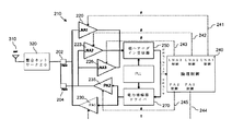
ここで、図2〜図10を参照すると、本発明のいくつかの例示的な実施形態に従って構成された集積回路デバイス200の例が示されている。集積回路デバイス200は、例えば、図1の無線通信ユニット100の無線周波数コンポーネントまたは回路106の少なくとも一部を実装するために使用され得る無線周波数集積回路(RFIC)を備えてもよい。従って、集積回路デバイス200は、RF送受信器モジュール210を備える。
Referring now to FIGS. 2-10, an example of an
RF送受信器モジュール210は、入力221、224、227で集積回路デバイスの外部接点202、204に動作可能に結合される複数の低雑音増幅器(LNA)モジュール220、223、226を備える。使用されている間、LNAモジュール220、223、226は、各外部接点202、204からRF信号を受信し、受信したRF信号を増幅し、かつ増幅したRF信号を出力222、225、228するよう配置される。LNAモジュール220、223、226の出力222、225、228は、受信器モジュールに動作可能に結合される。示した例では受信器モジュールは、超ヘテロダイン受信器250を備え、超ヘテロダイン受信器250は、LNAモジュール220、223、226から増幅されたRF信号を受信し、かつ受信した信号の復調および復号を行ってそこからデータを抽出する。その後、抽出されたデータは、一般的には255で示すように制御モジュール240に供給される。
The
RF送受信器モジュール210はさらに、複数の電力増幅器(PA)モジュール230、235を備える。複数の電力増幅器(PA)モジュール230、235は、その出力231、236で集積回路デバイス200の外部接点202、204に動作可能に結合され、使用されている間、送信されるRF信号をその入力232、237で受信し、送信されるRF信号を増幅し、かつ送信される増幅された信号を出力231、236するよう配置される。PA230、235の入力は、PAドライバ270に動作可能に結合される。示した例ではPAドライバ270は、制御モジュール240から送信されるデータを受信し(一般的には275で示すように)、送信されるデータの符号化および符号化されたデータを搬送するRF信号の変調を行い、かつ変調された増幅されるRF信号をPA230、235に提供するよう配置されている。
The
完全を期すために、例示された送受信器モジュール210はさらに、位相ルックループ(PLL)260を備え、位相ルックループ(PLL)260は、受信器250およびPAドライバ270に対するそれぞれタイミング基準信号262、264を生成するよう配置される。
For completeness, the illustrated
複数のLNA220、223、226および複数のPA230、235は、少なくとも第1のマルチアンテナ構成および第2の単一アンテナ高送信電力構成において動作するよう選択的に構成可能である。例えば、例示された送受信器モジュール210は、単一のアンテナ高送信電力構成において動作するよう選択的に構成され得る2つのPA230、235を備え、それにより送信されるRF信号はPA230、235の両方によって増幅される。その後、2つのPA230、235によって出力された増幅信号は、高送信電力信号を提供するよう組み合わされる。
The plurality of
示した例では、制御モジュール240は、複数のLNA220、223、226および複数のPA230、235を要求された送受信器構成において動作するよう選択的に構成するよう構成可能である。従って、制御モジュール240は、制御信号241、242、243、244、245をそれぞれ経由して、LNA220、223、226およびPA230、235のそれぞれに動作可能に結合される。
In the illustrated example, the
本発明のいくつかの例示的な実施形態に従って、複数のLNA220、223、226および複数のPA230、235は、デュアルアンテナ送受信器構成、単一アンテナ高送信電力送受信器構成、および単一アンテナ低送信電力送受信器構成、の群のうちの少なくとも1つにおいて動作するよう選択的に構成可能であり得る。
In accordance with some exemplary embodiments of the present invention,
図3および図4は、単一アンテナ低送信電力送受信器構成において動作するよう構成された送受信器モジュール210の例を示す。示した例では、送受信器モジュール210は、第1のLNA220を備え、第1のLNA220は、その入力221で集積回路デバイス200の第1の外部接点202に動作可能に結合され、かつ第1の外部接点202からRF信号を受信し、第1の外部接点202から受信されたRF信号を増幅し、かつ増幅信号を出力222するよう選択的に構成可能である。例示された送受信器モジュール210はさらに、第1のPA230を備え、第1のPA230は、その出力231で集積回路デバイス200の第1の外部接点202に動作可能に結合され、かつ送信されるRF信号をその入力232で受信し、受信された送信されるRF信号を増幅し、かつ増幅信号を第1の外部接点202に出力231するよう選択的に構成可能である。アンテナ310は、インピーダンス整合回路320を介して第1の外部接点202に動作可能に結合される。
3 and 4 illustrate an example of a
図3は、単一アンテナ310からのRF信号を受信するよう構成された送受信器モジュール210を示す。第1のLNA220は、アンテナ310からのRF信号を第1の外部接点202を介して受信し、受信したRF信号を増幅し、かつ増幅信号を受信器250に出力するよう、制御信号241を介して制御モジュール240によって制御される。残りのLNAモジュール223、226およびPAモジュール230、235は、制御信号242、243、244、245を介して制御モジュール240によって効率的に「ディセーブル」される。
FIG. 3 shows a
図4は、単一アンテナ310を介してRF信号を送信するように構成された送受信器モジュール210を示す。第1のPA230は、送信されるRF信号をその入力232で受信し、受信されたRF信号を増幅し、かつ増幅信号を外部接点202を介してアンテナ310に出力するよう、制御信号244を介して制御モジュール240によって制御される。LNA220、223、226および残りのPA235は、制御信号241、242、243、245を介して制御モジュール240によって効率的に「ディセーブル」される。
FIG. 4 shows a
従って、図3および図4で示すように、送受信器モジュール210は、制御モジュール240を経由して、単一アンテナ310を介してRF信号を送信および受信するよう選択的に制御されることが可能である。送受信器回路の効率性を最適化するために、例示された第1のLNA220および第1のPA230は、第1の外部接点202に対して互換性のある(例えば、実質的に等しい)インピーダンスを含むよう構成されてもよい。このように、インピーダンス整合回路320は、第1のLNA220および第1のPA230の両方で単一(共通)インピーダンスZ0を整合するよう構成されてもよい。
Thus, as shown in FIGS. 3 and 4,
図5〜図8は、デュアルアンテナ送受信器構成において動作するよう構成された送受信器モジュール210の例を示す。示した例では、送受信器モジュール210はさらに、第2のLNA223を備え、第2のLNA223は、その入力224で集積回路デバイス200の第2の外部接点204に動作可能に結合され、かつ第2の外部接点204からRF信号を受信し、第2の外部接点204から受信されたRF信号を増幅し、かつ増幅されたRF信号を出力225するよう選択的に構成可能である。送受信器モジュール210はさらに、第2のPA235を備え、第2のPA235は、その出力236で集積回路デバイス200の第2の外部接点204に動作可能に結合され、かつ送信されるRF信号をその入力237で受信し、受信された送信されるRF信号を増幅し、かつ増幅信号を第2の外部接点204に出力236するよう選択的に構成可能である。第1のアンテナ510は、第1のインピーダンス整合回路520を介して第1の外部接点202に動作可能に結合される。第2のアンテナ530は、第2のインピーダンス整合回路540を介して第2の外部接点204に動作可能に結合される。
5-8 illustrate an example of a
図5は、第1のアンテナ510からRF信号を受信するよう構成された送受信器モジュール210を示す。第1のLNA220は、第1のアンテナ510から第1の外部接点202を介してRF信号を受信し、受信したRF信号を増幅し、かつ増幅信号を受信器250に出力するよう、制御信号241を介して制御モジュール240によって制御される。残りのLNA223、226およびPA230、235は、制御信号242、243、244、245を介して制御モジュール240によって効率的に「ディセーブル」される。
FIG. 5 shows a
図6は、第2のアンテナ530からRF信号を受信するように構成された送受信器モジュール210を示す。第2のLNA223は、第2のアンテナ530から第2の外部接点204を介してRF信号を受信し、受信したRF信号を増幅し、かつ増幅信号を受信器250に出力するよう、制御信号242を介して制御モジュール240によって制御される。残りのLNA220、226およびPA230、235は、制御信号241、243、244、245を介して制御モジュール240によって効率的に「ディセーブル」される。
FIG. 6 shows a
図7は、第1のアンテナ510を介してRF信号を送信するよう構成された送受信器モジュール210を示す。第1のPA230は、その入力232で送信されるRF信号を受信し、受信されたRF信号を増幅し、かつ増幅信号を第1の外部接点202を介して第1のアンテナ510に出力するよう、制御信号244を介して制御モジュール240によって制御される。LNA220、223、226および残りのPAモジュール235は、制御信号241、242、243、245を介して制御モジュール240によって効率的に「ディセーブル」される。
FIG. 7 shows a
図8は、第2のアンテナ530を介してRF信号を送信するよう構成された送受信器モジュール210を示す。第2のPA235は、その入力237で送信されるRF信号を受信し、受信したRF信号を増幅し、かつ増幅信号を第2の外部接点204を介して第2のアンテナ530に出力するよう、制御信号245を介して制御モジュール240によって制御される。LNA220、223、226および残りのPAモジュール230は、制御信号241、242、243、244を介して制御モジュール240によって効率的に「ディセーブル」される。
FIG. 8 shows a
従って、図5〜図8で示すように、送受信器モジュール210は、制御モジュール240を経由して、例えばアンテナダイバーシティシステム内部で実装され得るように、2つのアンテナ510、530を介してRF信号を送信および受信するよう選択的に構成されることが可能である。送受信器回路の効率性を最適化するために、第2のLNA223および第2のPA235は、第1の外部接点202に対して互換性のある(例えば、実質的に等しい)インピーダンスを含むように構成される第1のLNA220および第1のPA230に加えて、第2の外部接点204に対して互換性のある(例えば、実質的に等しい)インピーダンスを含むように構成されてもよい。このように、インピーダンス整合回路520、540はそれぞれ、LNA220、223およびPA230、235の両方で単一(共通)インピーダンス(Z2)を整合するよう構成され得る。
Thus, as shown in FIGS. 5-8, the
一例として、第2のLNA223および第2のPA235は、図3および図4で示すような第1のLNA220および第1のPA230と同様に、単一アンテナ低送信電力送受信器構成において動作するよう同等に構成され得る。
As an example, the
図9および図10は、単一アンテナ高送信電力送受信器構成において動作するよう構成された送受信器モジュール210の例を示す。示した例では、送受信器モジュール210はさらに、第3のLNA226を備え、第3のLNA226は、その入力227で集積回路デバイス200の第2の外部接点204に動作可能に結合され、かつ第2の外部接点204からRF信号を受信し、第2の外部接点204から受信したRF信号を増幅し、かつ増幅されたRF信号を出力228するよう選択的に構成可能である。単一アンテナ910は、インピーダンス整合回路920を介して第1の外部接点202および第2の外部接点204に動作可能に結合される。
9 and 10 show an example of a
図9は、アンテナ910からRF信号を受信するよう構成された送受信器モジュール210を示す。第3のLNA226は、アンテナ910から第2の外部接点204を介してRF信号を受信し、受信されたRF信号を増幅し、かつ増幅信号を受信器250に出力するよう、制御信号243を介して制御モジュール240によって制御される。残りのLNA220、223およびPA230、235は、制御信号241、242、244、245を介して制御モジュール240によって効率的に「ディセーブル」される。
FIG. 9 shows a
図10は、アンテナ910を介してRF信号を送信するよう構成された送受信器モジュール210を示す。第1のPA230は、送信されるRF信号をその入力232で受信し、受信されたRF信号を増幅し、かつ増幅信号を第1の外部接点202を介してアンテナ910に出力するよう、制御信号244を介して制御モジュール240によって制御される。第2のPA235は、送信されるRF信号をその入力237で受信し、受信されたRF信号を増幅し、かつ増幅信号を第2の外部接点204を介してアンテナ910に出力するよう、制御信号245を介して制御モジュール240によって制御される。図示されるように、外部接点202、204は互いに動作可能に結合され、増幅信号を組み合わせて高送信電力信号を生成する。LNA220、223、226は、制御信号241、242、243を介して制御モジュール240によって効率的に「ディセーブル」される。
FIG. 10 shows a
従って、図9および図10で示すように、送受信器モジュール210は、制御モジュール240を経由して、単一アンテナ910を介してRF信号を送信および受信するよう選択的に構成することが可能である。具体的には、送受信器モジュール210は、第1のPA230および第2のPA235を使用して高送信電力で送信し、並列方式で信号を増幅できる。送受信器回路の効率性を高めるため、第3のLNA226は、第1の外部接点202および第2の外部接点204に対して、並列に動作可能に結合されている場合、第1のPA230および第2のPA235と互換性のある(例えば、実質的に等しい)インピーダンスを含んでもよい。このように、インピーダンス整合回路920は、並列方式で構成される第3のLNA226およびPA230、235の両方で単一(共通)インピーダンス(Z1)を整合するよう構成されてもよい。
Accordingly, as shown in FIGS. 9 and 10, the
受信チェーンでは、LNA最適インピーダンスは、LNA入力インピーダンスまたは中間最小雑音インピーダンスによって定義され得る。一例では、このインピーダンスは、設計段階の間に定義されてもよく、能動デバイスバイアス状況、能動および受動コンポーネント、サイジングなどによって異なり得る。その後、広域の入力インピーダンス範囲に渡り、性能が改善されたLNAを開発することが可能となる。それにもかかわらず、外部整合ネットワークの損失を最小化するために、一例では、LNA入力インピーダンスは、アンテナインピーダンス(例えば10〜200オーム)とほぼ同じになるよう構成されてもよい。 In the receive chain, the LNA optimum impedance may be defined by the LNA input impedance or the medium minimum noise impedance. In one example, this impedance may be defined during the design phase and may vary depending on active device bias conditions, active and passive components, sizing, and the like. Thereafter, it becomes possible to develop an LNA with improved performance over a wide input impedance range. Nevertheless, in order to minimize loss of the external matching network, in one example, the LNA input impedance may be configured to be approximately the same as the antenna impedance (eg, 10-200 ohms).
送信チェーンでは、PAインピーダンスは、PAの出力インピーダンスとして定義されないが、最大の効率性で最大の電力送信を有するために、PAに与える最適なインピーダンスとして定義される。ほとんどの時間をパルス制御電流を使用して「オン」/「オフ」切り替え方式で動作するよう構成されるPAもあるので、上限は、負荷に提供され得る最大電圧によって与えられてもよい。オームの法則を考慮すると、負荷インピーダンス、供給電圧およびパルス電流値は、互いに関連がある。従って、小さな電流で比較的大きなインピーダンスを使用すること、または大きな電流で低いインピーダンスを使用することが可能となり、どちらも同じ電力を提供するよう構成され得る。しかしながら、整合ネットワークの損失を最小化するため、1つの例示的な実施形態は、例えば10〜200オームのような比較的低いインピーダンスを選択し得る。 In the transmit chain, the PA impedance is not defined as the output impedance of the PA, but is defined as the optimal impedance to give the PA in order to have maximum power transmission with maximum efficiency. Since some PAs are configured to operate in an “on” / “off” switching manner using pulsed control current most of the time, the upper limit may be given by the maximum voltage that can be provided to the load. Considering Ohm's law, load impedance, supply voltage and pulse current value are related to each other. Thus, it is possible to use a relatively large impedance with a small current, or a low impedance with a large current, both of which can be configured to provide the same power. However, to minimize matching network loss, one exemplary embodiment may select a relatively low impedance, such as 10-200 ohms.
PAがICの内部で開発されると、製品設計者は、2つ以上のPAが同じ電圧で2倍(または実質的に倍)の電流を提供するために並列に構成された送受信器を設計することが可能になる。このように、改善された/最適の性能のためにインピーダンスは、半減されてもよく、またはさらに削減されてもよい。一例では、共通の整合ネットワークが並列のPAを利用する構成において使用される場合、別のLNAは、半分のインピーダンスで組み込まれ、かつ設計されてもよい。 When a PA is developed inside an IC, product designers design a transceiver configured in parallel so that two or more PAs provide twice (or substantially twice) current at the same voltage It becomes possible to do. In this way, the impedance may be halved or further reduced for improved / optimal performance. In one example, if a common matching network is used in a configuration that utilizes parallel PAs, another LNA may be incorporated and designed with half impedance.
一例では、第1のLNA220および第2のLNA223は、第1のPA230および第2のPA235のインピーダンスそれぞれと実質的に等しいインピーダンスを含むよう構成されてもよい。このように、送受信器モジュール210が、図3および図4に示されるような単一アンテナ低送信電力構成、または図5〜図8に示されるようなデュアルアンテナ送受信器構成のいずれかで動作する場合、アンテナと送受信器モジュール210との間の正確なインピーダンス整合が、達成され得る。従って、最適なPAインピーダンスは、一般的に利用可能な供給電圧およびPA電流源の能力によって定義されるが、達成され得る。
In one example, the
しかしながら、図9および図10に示されるように、送受信器モジュールが単一アンテナ高送信電力送受信器構成で動作している場合、2つのPA230、235は並列で動作するよう構成されるため、実質的に2倍の電流は、インピーダンス整合回路920に出力され、結果としてインピーダンス整合回路910によって供給される必要な負荷インピーダンスの約半分をもたらす。結果として、インピーダンス整合回路910は、もはや第1のLNA220および第2のLNA223と互換性を持たない。従って、単一アンテナ高送信電力送受信動作の間に使用する第3のLNA226を提供することによって、第3のLNA226は、インピーダンス整合回路910によって提供される低負荷インピーダンスと互換性を持つように構成されてもよい。例えば低負荷インピーダンスは、第1のLNA220および第2のLNA223の入力インピーダンスの実質的に半分を含む。LNA入力インピーダンスは、一般的に集積回路デバイスの設計段階で定義される(例えば、MOS(金属酸化物半導体)ゲートサイズ、コイル値、バイアス電流などの調整を通じて)。
However, as shown in FIGS. 9 and 10, when the transceiver module is operating in a single antenna high transmit power transceiver configuration, the two
重要な点として、示された例では、高送信電力構成を含む各送受信器構成において、共通の外部接点が送信および受信チェーンの両方で使用されるため、追加の有益な外部接点が利用されることの必要性は実質的になくなる。 Importantly, in the example shown, an additional beneficial external contact is utilized in each transceiver configuration, including a high transmit power configuration, since a common external contact is used in both the transmit and receive chains. The need for this is virtually eliminated.
少なくとも第1のマルチアンテナ構成および第2の単一アンテナ高送信電力構成において動作するよう選択的に構成されるように集積回路デバイス200の送受信器モジュール210内にLNAおよびPAを構成することによって、集積回路デバイス200は、異なる送受信器構成の送受信器機能を提供できる。具体的には、集積回路デバイスは、マルチアンテナ構成または単一アンテナ構成内で送受信器機能を提供し得る。示された例では、集積回路デバイス200は、上記で説明し添付の図面で示すように、デュアルアンテナ送受信器構成、低送信電力単一アンテナ構成、または高送信電力構成内で送受信器機能を提供できる。
By configuring the LNA and PA in the
一例では、並列PAネットワークと互換性を持つよう構成された追加のLNAを組み込むとともに、集積回路(または無線通信ユニット)の1つ以上の以下の要素、すなわち、少なくとも1つのPAの論理制御、少なくとも1つのPAドライバ回路の論理制御は、構成され得る。動作の第1のモードにおいて、集積回路はアンテナダイバーシティに利用されてもよい。動作の第1のモードにおいて、第1のLNAおよび第1のPAは、第2のアンテナ要素に動作可能に結合された第2のLNAおよび第2のPAとともに、両方とも第1のアンテナ要素(例えば、アンテナアレイ)に動作可能に結合されてもよい。このように、アンテナダイバーシティは、2つのそれぞれのアンテナ要素を介して同じ信号を送信/受信することによって達成され得る。動作の第2のモードにおいて、例えば、動作のアンテナダイバーシティモードで使用されるLNAよりも低いインピーダンスを示すよう追加のLNAを構成することが可能である。このように、単一アンテナ要素は、高電力印加のために使用されてもよい。例えば、追加のLNAは動作の第2のモードである受信モードで使用されてもよいのに対して、2以上のPAは、送信モードで同時に使用され得る。このように、高電力構成の送信モードにおいて、集積回路(または無線通信ユニット)の電位出力電力を、上記の動作の第1(アンテナダイバーシティ)モードと比較しておおよそ2倍にすることが可能となり得る。 In one example, an additional LNA configured to be compatible with a parallel PA network is incorporated, and one or more of the following elements of an integrated circuit (or wireless communication unit), ie, logical control of at least one PA, at least The logic control of one PA driver circuit can be configured. In the first mode of operation, the integrated circuit may be utilized for antenna diversity. In the first mode of operation, the first LNA and the first PA together with the second LNA and the second PA operably coupled to the second antenna element are both the first antenna element ( For example, it may be operably coupled to an antenna array. In this way, antenna diversity can be achieved by transmitting / receiving the same signal via two respective antenna elements. In the second mode of operation, for example, additional LNAs can be configured to exhibit a lower impedance than the LNA used in the antenna diversity mode of operation. Thus, a single antenna element may be used for high power application. For example, additional LNAs may be used in the receive mode, which is the second mode of operation, while two or more PAs may be used simultaneously in the transmit mode. Thus, in the transmission mode of the high power configuration, the potential output power of the integrated circuit (or the wireless communication unit) can be approximately doubled compared to the first (antenna diversity) mode of the above operation. obtain.
このように、単一の集積回路デバイスは、異なる送受信器構成を利用するさまざまな異なる用途内で使用できるよう開発されることができ、このような集積回路デバイスの設計および開発の時間スケールおよびコストを大幅に削減する。重要な点として、このような集積回路デバイスのコストが削減されるだけでなく、このような集積回路デバイスを備える無線通信ユニットの材料費も削減される。 Thus, a single integrated circuit device can be developed for use in a variety of different applications that utilize different transceiver configurations, and the time scale and cost of the design and development of such an integrated circuit device. Drastically reduce. Importantly, not only is the cost of such an integrated circuit device reduced, but the material cost of a wireless communication unit comprising such an integrated circuit device is also reduced.
さらに、集積回路デバイスは異なる送受信器構成をサポートできるので、異なる送信技術をサポートできる無線通信ユニットが提供され、異なる送受信器構成を必要としてもよく、異なる送受信機構成は、無線通信ユニットとは、集積回路デバイスに結合されたアンテナおよびインピーダンス整合回路構成によってのみ異なる(ハードウェアの点で)。重要な点として、同じ集積回路デバイス200が異なる送受信器構成を提供するために使用され得るので、集積回路デバイスに「隠れた」残りの無線通信ユニットは、異なる送信技術用に重複されてもよい。これはこのような無線通信デバイスの開発コストおよび時間スケールを大幅に削減する。
In addition, because integrated circuit devices can support different transceiver configurations, wireless communication units that can support different transmission technologies are provided and may require different transceiver configurations, and different transceiver configurations are defined as wireless communication units. It depends only on the antenna and impedance matching circuit configuration coupled to the integrated circuit device (in terms of hardware). Importantly, because the same
次に図11を参照すると、例えば図1の無線通信ユニット100を製造するために実装され得るようないくつかの例示的な実施形態に従って、無線通信システムを製造する方法の簡略化されたフローチャート1100の例が示されている。この方法は、ステップ1110で開始され、無線通信ユニットのRF送受信器構成を決定することによって、ステップ1120に移動する。例えば、ステップ1120は、デュアルアンテナ送受信器構成、単一アンテナ高送信電力送受信器構成、および単一アンテナ低送信電力送受信器構成からなる群から、RF送受信器構成を選択することを含む。
Referring now to FIG. 11, a
次に、ステップ1130において、この方法は、例えば図3〜図10に示されるアンテナおよび整合ネットワーク構成の1つのような、決定されたRF送受信器構成のために必要なアンテナおよび整合ネットワーク構成を選択することを含む。その後、ステップ1140において、RF送受信器回路は、選択されたアンテナおよび整合ネットワーク構成、および図2の集積回路デバイス200のような、少なくとも第1のマルチアンテナ構成および第2の単一アンテナ高送信電力構成において動作するよう構成され得るRF送受信器モジュールを備える集積回路デバイスを含むように組み立てられる。次に、ステップ1150において、集積回路デバイスのRF送受信器モジュールは、決定されたRF送受信器構成に従って動作するよう構成される。設計方法はその後、1160において終了する。設計方法は集積回路を製造する方法の一部であってもよく、設計方法が終了した後、集積回路はフォトマスクの図柄に従って製造され得ることが明らかであろう。
Next, in
本発明の例示されている実施形態は、大部分について、当業者に既知の電子コンポーネントおよび回路を使用して実装され得るため、本発明の基礎となる概念の理解および評価のために、ならびに本発明の教示を分かりにくくせず当該教示から注意を逸らさせないために、詳細は上記で例示されているような必要と考えられる範囲を超えては説明されない。 The illustrated embodiments of the present invention can be implemented, for the most part, using electronic components and circuits known to those skilled in the art, for the understanding and evaluation of the concepts underlying the present invention, as well as in this book. In order not to obscure the teachings of the invention or to distract from the teachings, details are not described beyond what is considered necessary, as exemplified above.
本発明は、コンピュータシステムのようなプログラム可能な機器上で起動する場合に本発明による方法のステップを行うための、またはプログラム可能な機器が本発明によるデバイスまたはシステムの機能を実行できるようにするための、コード部分を少なくとも含む、コンピュータシステム上で起動するコンピュータプログラム内の少なくとも一部(例えば、制御モジュール240のすべてまたは一部、および/または図11の方法のすべてまたは一部)に実装できる。
The invention is for performing the steps of the method according to the invention when booted on a programmable device such as a computer system, or enabling a programmable device to carry out the functions of a device or system according to the invention. Can be implemented in at least a part (eg, all or part of the
コンピュータプログラムは、特定のアプリケーションプログラムおよび/またはオペレーティングシステムのような、命令のリストである。コンピュータプログラムは例えば、サブルーチン、関数、プロシージャ、オブジェクトメソッド、オブジェクトインプリメンテーション、実行可能アプリケーション、アプレット、サーブレット、ソースコード、オブジェクトコード、共有ライブラリ/動的ロードライブラリ、および/または、コンピュータシステム上での実行のために設計される他の一連の命令のうちの1つまたは複数を含むことができる。 A computer program is a list of instructions, such as a particular application program and / or operating system. A computer program can be, for example, a subroutine, function, procedure, object method, object implementation, executable application, applet, servlet, source code, object code, shared library / dynamic load library, and / or on a computer system One or more of a series of other instructions designed for execution may be included.
コンピュータプログラムはコンピュータ可読記憶媒体上に内部的に記憶されるか、またはコンピュータ可読伝送媒体を介してコンピュータシステムに送信されることができる。コンピュータプログラムのすべてまたはいくつかは、情報処理システムに永続的に、取り外し可能に、または遠隔的に結合されるコンピュータ可読媒体上で提供されることができる。コンピュータ可読媒体は例えば、限定されることなく、いくつか例を挙げると、ディスクおよびテープ記憶媒体を含む磁気記憶媒体、コンパクトディスク媒体(例えば、CD−ROM、CD−Rなど)およびデジタルビデオディスク記憶媒体を含む光記憶媒体、フラッシュメモリ、EEPROM、EPROM、ROMのような半導体ベースのメモリユニットを含む不揮発性メモリ記憶媒体、強磁性デジタルメモリ、MRAM、レジスタ、バッファまたはキャッシュ、メインメモリ、RAMなどを含む揮発性記憶媒体、ならびにコンピュータネットワーク、ポイントツーポイント遠隔通信機器、および搬送波伝送媒体を含むデータ伝送媒体のうちの任意の数を含むことができる。 The computer program can be stored internally on a computer readable storage medium or transmitted to a computer system via a computer readable transmission medium. All or some of the computer program may be provided on a computer readable medium that is permanently, removably or remotely coupled to the information processing system. Computer-readable media include, but are not limited to, magnetic storage media, including disk and tape storage media, compact disk media (eg, CD-ROM, CD-R, etc.) and digital video disk storage, to name a few examples. Optical storage media including media, non-volatile memory storage media including semiconductor-based memory units such as flash memory, EEPROM, EPROM, ROM, ferromagnetic digital memory, MRAM, registers, buffers or caches, main memory, RAM, etc. It may include any number of volatile storage media including, and data transmission media including computer networks, point-to-point telecommunications equipment, and carrier wave transmission media.
コンピュータプロセスは通常、実行している(作動している)プログラムまたはプログラムの一部、現在のプログラム値および状態情報、ならびにプロセスの実行を管理するためにオペレーティングシステムによって使用されるリソースを含む。オペレーティングシステム(OS)は、コンピュータのリソースの共有を管理するとともにプログラマにこれらのリソースにアクセスするために使用されるインタフェースを提供するソフトウェアである。オペレーティングシステムは、システムデータおよびユーザ入力を処理して、タスクおよび内部システムリソースをシステムのユーザおよびプログラムに対するサービスとして配分および管理することによって応答する。 A computer process typically includes a running program or part of a program, current program values and state information, and resources used by the operating system to manage the execution of the process. An operating system (OS) is software that manages the sharing of computer resources and provides an interface for programmers to access these resources. The operating system responds by processing system data and user input to allocate and manage tasks and internal system resources as services to system users and programs.
コンピュータシステムは例えば、少なくとも1つの処理装置、関連付けられるメモリ、および多数の入出力(I/O)デバイスを含むことができる。コンピュータプログラムを実行する時、コンピュータシステムはコンピュータプログラムに従って情報を処理して、結果としての出力情報をI/Oデバイスを介して生成する。 A computer system can include, for example, at least one processing unit, associated memory, and multiple input / output (I / O) devices. When executing the computer program, the computer system processes the information according to the computer program and generates the resulting output information via the I / O device.
上記の明細書において、本発明が本発明の実施形態の具体例を参照して説明された。しかしながら、添付の特許請求の範囲に記載されている本発明のより広い精神および範囲から逸脱することなく、そこにさまざまな修正および変更を行うことができることは明らかであろう。 In the foregoing specification, the invention has been described with reference to specific examples of embodiments of the invention. However, it will be apparent that various modifications and changes may be made thereto without departing from the broader spirit and scope of the invention as set forth in the appended claims.
本明細書において説明されているような接続は、例えば介在するデバイスを介してそれぞれのノード、ユニットまたデバイスから、またはそれらへと信号を転送するのに適切な任意のタイプの接続であることができる。従って、別途暗示または提示されていない限り、接続は例えば直接接続であってもよいし、間接接続であってもよい。接続は、単一の接続、複数の接続、一方向性接続、または双方向性接続であることに関連して例示または記載され得る。しかしながら、実施形態が異なれば、接続の実施態様は変化してもよい。例えば、双方向性接続ではなく別個の一方向性接続が使用されてもよく、その逆であってもよい。さらに、複数の接続が、連続してまたは時分割多重方式で複数の信号を伝送する単一の接続と置き換わってもよい。同様に、複数の信号を搬送する単一の接続が、これらの信号のサブセットを搬送するさまざまな異なる接続に分離されてもよい。それゆえ、信号の伝送には多くの選択肢が存在する。 A connection as described herein can be any type of connection suitable for transferring signals to or from each node, unit or device, for example, via an intervening device. it can. Therefore, unless otherwise implied or presented, the connection may be a direct connection or an indirect connection, for example. A connection may be illustrated or described in connection with being a single connection, multiple connections, a unidirectional connection, or a bidirectional connection. However, the connection implementation may vary for different embodiments. For example, a separate unidirectional connection may be used instead of a bidirectional connection, and vice versa. Further, multiple connections may replace a single connection that transmits multiple signals in a continuous or time division multiplexed manner. Similarly, a single connection carrying multiple signals may be separated into a variety of different connections carrying a subset of these signals. Therefore, there are many options for signal transmission.
特定の導電型または電位の極性が記載され、例に示されているが、導電型および電位の極性は逆になってもよいことが理解されるだろう。
本明細書において記載されている各信号は正または負の論理として設計され得る。負論理信号の場合、信号は、論理的真状態が論理レベル0に対応するアクティブ・ローである。正論理信号の場合、信号は、論理的真状態が論理レベル1に対応するアクティブ・ハイである。本明細書に記載される信号はいずれも負または正論理信号のいずれかとして設計されることができることに留意されたい。それゆえ、代替の実施形態では、正論理信号として記載される信号は、負論理信号として実装されてもよく、負論理信号として記載される信号は、正論理信号として実装されてもよい。
Although a particular conductivity type or potential polarity is described and shown in the examples, it will be understood that the conductivity type and potential polarity may be reversed.
Each signal described herein may be designed as positive or negative logic. In the case of a negative logic signal, the signal is active low where the logical true state corresponds to logic level zero. In the case of a positive logic signal, the signal is active high with a logical true state corresponding to logic level one. Note that any of the signals described herein can be designed as either negative or positive logic signals. Thus, in alternative embodiments, signals described as positive logic signals may be implemented as negative logic signals, and signals described as negative logic signals may be implemented as positive logic signals.
論理ブロック間の境界は例示にすぎないこと、および、代替的な実施形態は、論理ブロックもしくは回路要素を融合し、またはさまざまな論理ブロックもしくは回路要素に対する代替的な機能の分解を課してもよいことを、当業者は認識しよう。従って、本明細書において描写したアーキテクチャは例示にすぎないこと、および、事実、同じ機能を達成する多くの他のアーキテクチャを実装できることは理解されたい。例えば、示された例では、制御モジュール240、受信器250、PLL260、およびPAドライバ270は、独立した論理ブロックとして示されている。しかしながら、これらの各機能は、任意の適切な代替方式に分散および/または統合できることが理解されよう。
The boundaries between logic blocks are only exemplary, and alternative embodiments may merge logic blocks or circuit elements or impose alternative functional decompositions on various logic blocks or circuit elements. Those skilled in the art will recognize that this is good. Thus, it should be understood that the architecture depicted herein is merely exemplary, and in fact many other architectures that accomplish the same function can be implemented. For example, in the illustrated example,
同じ機能を達成するための構成要素の任意の構成が、所望の機能が達成されるように効果的に「関連付けられる」。従って、本明細書における、特定の機能を達成するために結合される任意の2つの構成要素は互いに「関連付けられる」とみなすことができ、それによって、中間の構成要素またはアーキテクチャにかかわりなく、所望の機能が達成される。同様に、そのように関連付けられる任意の2つの構成要素も、所望の機能を達成するために互いに「動作可能に接続されている」または「動作可能に結合されている」とみなすことができる。 Any configuration of components to achieve the same function is effectively “associated” so that the desired function is achieved. Thus, any two components in this document that are combined to achieve a particular function can be considered “associated” with each other, so that no matter what intermediate component or architecture is desired. The function is achieved. Similarly, any two components so associated may be considered “operably connected” or “operably coupled” to each other to achieve a desired function.
さらに、上述の動作間の境界は例示にすぎないことを当業者は認識しよう。複数の動作を単一の動作に組み合わせ、単一の動作を追加の動作に分散させ、複数の動作を少なくとも部分的に時間的に重ね合わせて実行できる。その上、代替的な実施形態は、特定の動作の複数のインスタンスを含んでもよく、動作の順序はさまざまな他の実施形態においては変更してもよい。 Moreover, those skilled in the art will recognize that the boundaries between the above operations are exemplary only. Multiple operations can be combined into a single operation, a single operation can be distributed over additional operations, and multiple operations can be performed at least partially overlapping in time. Moreover, alternative embodiments may include multiple instances of a particular operation, and the order of operations may be changed in various other embodiments.
さらに例として、実施例、またはその一部は、任意の適切なタイプのハードウェア記述言語などによって、実回線または実回線に転換可能な論理表現のソフトまたはコード表現として実装されることができる。 By way of further example, the embodiments, or portions thereof, may be implemented as a software or code representation of a logical representation that can be converted to a real line or a real line, such as by any suitable type of hardware description language.
さらに、本発明は、プログラム不能ハードウェアにおいて実装される物理デバイスまたはユニットに限定されるものではなく、本出願においては一般的に「コンピュータシステム」として示されている、メインフレーム、ミニコンピュータ、サーバ、ワークステーション、パーソナルコンピュータ、ノートパッド、携帯情報端末、電子ゲーム、自動車および他の組込みシステム、携帯電話、ならびに、さまざまな他の無線デバイスのような、適切なプログラムコードに従って操作することによって所望のデバイス機能を実行することが可能なプログラム可能デバイスまたはユニット内に適用されることもできる。 Further, the present invention is not limited to physical devices or units implemented in non-programmable hardware, and is generally referred to as a “computer system” in this application as a mainframe, minicomputer, server. Desired by operating according to appropriate program code, such as workstations, personal computers, notepads, personal digital assistants, electronic games, automobiles and other embedded systems, mobile phones, and various other wireless devices It can also be applied within a programmable device or unit capable of performing device functions.
しかしながら、他の修正形態、変更形態および代替形態も可能である。従って、明細書および図面は限定的な意味においてではなく例示的に考慮されるべきである。
特許請求の範囲において、括弧間に置かれる任意の参照符号は特許請求の範囲を限定するものとして解釈されるべきではない。「備える(comprising)」という文言は、特許請求項内にリストされているもの以外の要素またはステップの存在を除外するものではない。さらに、本明細書において使用される場合、「1つ("a"or"an")」という用語は、1つまたは2つ以上として定義される。さらに、特許請求の範囲における「少なくとも1つの」および「1つまたは複数の」のような前置きの語句の使用は、不定冠詞「1つの("a"or"an")」による別の請求項要素の導入が、このように導入された請求項要素を含む任意の特定の請求項を、たとえ同じ請求項が前置きの語句「1つまたは複数の」または「少なくとも1つの」および「1つの("a"or"an")」のような不定冠詞を含む場合であっても、1つだけのこのような要素を含む発明に限定することを暗示するように解釈されるべきではない。同じことが、定冠詞の使用についても当てはまる。別途記載されない限り、「第1の」および「第2の」のような用語は、そのような用語が説明する要素間で適宜区別するように使用される。従って、これらの用語は必ずしも、このような要素の時間的なまたは他の優先順位付けを示すようには意図されていない。特定の手段が相互に異なる特許請求項において記載されているというだけの事実は、これらの手段の組み合わせを有利に使用することができないということを示すものではない。
However, other modifications, changes and alternatives are possible. The specification and drawings are, accordingly, to be regarded in an illustrative rather than a restrictive sense.
In the claims, any reference signs placed between parentheses shall not be construed as limiting the claim. The word “comprising” does not exclude the presence of elements or steps other than those listed in a claim. Further, as used herein, the term “a” or “an” is defined as one or more. Further, the use of the introductory phrases such as “at least one” and “one or more” in the claims is subject to another claim by the indefinite article “a” or “an”. The introduction of an element refers to any particular claim that includes the claim element thus introduced, even if the same claim is preceded by the words “one or more” or “at least one” and “one ( The inclusion of indefinite articles such as “a” or “an”) ”should not be construed to imply limiting to inventions that include only one such element. The same is true for the use of definite articles. Unless stated otherwise, terms such as “first” and “second” are used to appropriately distinguish between the elements such terms describe. Thus, these terms are not necessarily intended to indicate temporal or other prioritization of such elements. The mere fact that certain measures are recited in mutually different claims does not indicate that a combination of these measured cannot be used to advantage.
Claims (13)
複数の低雑音増幅器(220、223、226)であって、前記複数の低雑音増幅器(220、223、226)はそれぞれ、入力ポート(221、224、227)を有し、前記複数の低雑音増幅器(220、223、226)は、前記集積回路デバイス(200)の少なくとも1つの外部接点(202、204)に動作可能に結合され、かつ前記少なくとも1つの外部接点(202、204)から第1のRF信号を受信し、増幅された受信した第1のRF信号を出力(222、225、228)するよう構成されていることと;
複数の電力増幅器(230、235)であって、前記複数の電力増幅器(230、235)はそれぞれ、出力ポート(231、236)を有し、前記複数の電力増幅器(230、235)は、前記集積回路デバイス(200)の前記少なくとも1つの外部接点(202、204)に動作可能に結合され、かつ各電力増幅器入力ポート(232、237)で第2のRF信号を受信し、増幅された送信される第2のRF信号を出力(231、236)するように構成されることと
を含み、
前記複数の低雑音増幅器(220、223、226)および前記複数の電力増幅器(230、235)は、少なくとも第1のマルチアンテナ構成および第2の単一アンテナ高送信電力構成において動作するよう選択的に構成可能である、集積回路デバイス(200)。 An integrated circuit device (200) comprising at least one RF transceiver module (210), the at least one RF transceiver module (210) comprising:
A plurality of low-noise amplifiers (220, 223, 226), each of the plurality of low-noise amplifiers (220, 223, 226) having an input port (221, 224, 227); An amplifier (220, 223, 226) is operably coupled to at least one external contact (202, 204) of the integrated circuit device (200) and is first from the at least one external contact (202, 204). Configured to output (222, 225, 228) an amplified first received RF signal;
A plurality of power amplifiers (230, 235), each of the plurality of power amplifiers (230, 235) having an output port (231, 236), and the plurality of power amplifiers (230, 235) An operative transmission coupled to the at least one external contact (202, 204) of the integrated circuit device (200) and receiving a second RF signal at each power amplifier input port (232, 237) Configured to output (231, 236) a second RF signal to be
The plurality of low noise amplifiers (220, 223, 226) and the plurality of power amplifiers (230, 235) are selectively operable in at least a first multi-antenna configuration and a second single-antenna high transmission power configuration. An integrated circuit device (200) configurable.
請求項1に記載の集積回路デバイス(200)。 The plurality of low noise amplifiers (220, 223, 226) and the plurality of power amplifiers (230, 235) include a multi-antenna transceiver configuration, a single antenna high transmission power transceiver configuration, and a single antenna low transmission power transceiver. Is selectively configurable to operate in at least one of the group of configurations,
The integrated circuit device (200) of claim 1.
その入力(221)で前記集積回路デバイス(200)の第1の外部接点(202)に動作可能に結合され、かつ前記第1の外部接点(202)から前記第1のRF信号を受信し、増幅された第1のRF信号を出力(222)するよう選択的に構成可能である第1の低雑音増幅器(220)と;
その入力(224)で前記集積回路デバイス(200)の第2の外部接点(204)に動作可能に結合され、かつ前記第2の外部接点(204)から前記第1のRF信号を受信し、増幅された第1のRF信号を出力(225)するよう選択的に構成可能である第2の低雑音増幅器(223)と
を備える、
請求項1または請求項2に記載の集積回路デバイス(200)。 When the RF transceiver module (210) is configured to operate in the first multi-antenna configuration, the RF transceiver module (210)
Operably coupled at its input (221) to a first external contact (202) of the integrated circuit device (200) and receiving the first RF signal from the first external contact (202); A first low noise amplifier (220) that is selectively configurable to output (222) an amplified first RF signal;
Operably coupled to a second external contact (204) of the integrated circuit device (200) at its input (224) and receiving the first RF signal from the second external contact (204); A second low noise amplifier (223) that is selectively configurable to output (225) an amplified first RF signal;
An integrated circuit device (200) according to claim 1 or claim 2.
その出力(231)で前記集積回路デバイス(200)の第1の外部接点(202)に動作可能に結合され、かつ送信される前記第2のRF信号をその入力(232)で受信し、増幅された送信される第2のRF信号を前記第1の外部接点(202)に出力(231)するよう選択的に構成可能である第1の電力増幅器(230)と;
その出力(236)で前記集積回路デバイス(200)の第2の外部接点(204)に動作可能に結合され、かつ送信される前記第2のRF信号をその入力(237)で受信し、増幅された送信される前記第2のRF信号を前記第2の外部接点(204)に出力(236)するよう選択的に構成可能である第2の電力増幅器(235)と
を備える、
請求項1乃至3のいずれか1項に記載の集積回路デバイス(200)。 When the RF transceiver module (210) is configured to operate in the first multi-antenna configuration, the RF transceiver module (210)
The output (231) is operably coupled to the first external contact (202) of the integrated circuit device (200) and transmitted and receives and amplifies the second RF signal transmitted at the input (232). A first power amplifier (230) that is selectively configurable to output (231) the transmitted second RF signal to the first external contact (202);
The output (236) is operably coupled to a second external contact (204) of the integrated circuit device (200) and transmitted at the input (237) for receiving and amplifying the second RF signal to be transmitted. A second power amplifier (235) selectively configurable to output (236) the transmitted second RF signal transmitted to the second external contact (204);
An integrated circuit device (200) according to any one of the preceding claims.
請求項4に記載の集積回路デバイス(200)。 The first low-noise amplifier (220) and the first power amplifier (230) are configured to have impedances compatible with the first external contact (202);
The integrated circuit device (200) of claim 4.
前記第3の低雑音増幅器(226)は、その入力(227)で前記集積回路デバイス(200)の第1の外部接点(202)および第2の外部接点(204)のうちの少なくとも1つに動作可能に結合され、かつ少なくとも前記複数の低雑音増幅器の他の低雑音増幅器(220、223)よりも少ない係数の入力インピーダンスを有する、
請求項1乃至5のいずれか1項に記載の集積回路デバイス(200)。 The plurality of low noise amplifiers (220, 223, 226) includes a third low noise amplifier (226),
The third low noise amplifier (226) has at its input (227) at least one of a first external contact (202) and a second external contact (204) of the integrated circuit device (200). Operably coupled and having an input impedance with a coefficient that is at least less than other low noise amplifiers (220, 223) of the plurality of low noise amplifiers;
An integrated circuit device (200) according to any one of the preceding claims.
請求項6に記載の集積回路デバイス(200)。 The third low noise amplifier (226) is selectively controlled for use in a receive mode of operation in the second single antenna high transmit power configuration;
The integrated circuit device (200) of claim 6.
請求項6または請求項7に記載の集積回路デバイス(200)。 The plurality of power amplifiers (230, 235) are configured such that the second RF signal is amplified by at least two power amplifiers (230, 235) and output to the at least one external contact (202, 204) (231, 236) is selectively controlled to operate in the second single antenna high transmit power configuration by configuring the integrated circuit device (200) to
8. An integrated circuit device (200) according to claim 6 or claim 7.
請求項8に記載の集積回路デバイス(200)。 When the third low noise amplifier (226) is operably coupled in parallel with the first external contact (202) and the second external contact (204), Comprising an impedance compatible with a power amplifier and said second power amplifier (230, 235);
The integrated circuit device (200) of claim 8.
前記制御モジュール(240)は、前記複数の低雑音増幅器(220、223、226)および前記複数の電力増幅器(230、235)が少なくとも前記第1のマルチアンテナ構成および前記第2の単一アンテナ高送信電力構成において動作するよう選択的に制御されるよう構成される、
請求項1乃至9のいずれか1項に記載の集積回路デバイス(200)。 The RF transceiver module (210) further comprises a control module (240),
The control module (240) includes the plurality of low noise amplifiers (220, 223, 226) and the plurality of power amplifiers (230, 235) at least in the first multi-antenna configuration and the second single antenna height. Configured to be selectively controlled to operate in a transmit power configuration;
An integrated circuit device (200) according to any one of the preceding claims.
前記無線通信ユニット用のRF送受信器構成を決定すること(1120)と;
決定された前記RF送受信器構成に必要なアンテナおよび整合ネットワーク構成を選択すること(1130)と;
選択されたアンテナおよび整合ネットワーク構成を備える前記集積回路用のRF送受信器回路を、構成可能な第1のマルチアンテナ構成、および構成可能な第2の単一アンテナ高送信電力構成からなる群のうちの少なくとも1つにおいて動作するよう組み立てること(1140)と;
前記集積回路デバイスのRF送受信器モジュールを決定されたRF送受信器構成に従って動作するよう構成すること(1150)と
を有する方法。 A method (1100) for generating an integrated circuit design for a wireless communication unit, the method comprising:
Determining (1120) an RF transceiver configuration for the wireless communication unit;
Selecting the required antenna and matching network configuration for the determined RF transceiver configuration (1130);
An RF transceiver circuit for an integrated circuit comprising a selected antenna and a matching network configuration is comprised of a configurable first multi-antenna configuration and a configurable second single antenna high transmit power configuration Assembling to operate in at least one of (1140);
Configuring (1150) the RF transceiver module of the integrated circuit device to operate according to the determined RF transceiver configuration.
請求項12に記載の方法。 The method further includes fabricating the integrated circuit according to the design.
The method of claim 12.
Applications Claiming Priority (1)
| Application Number | Priority Date | Filing Date | Title |
|---|---|---|---|
| PCT/IB2010/003022 WO2012049529A1 (en) | 2010-10-15 | 2010-10-15 | Integrated circuit device, wireless communication unit and method of manufacture therefor |
Publications (1)
| Publication Number | Publication Date |
|---|---|
| JP2013539947A true JP2013539947A (en) | 2013-10-28 |
Family
ID=43984100
Family Applications (1)
| Application Number | Title | Priority Date | Filing Date |
|---|---|---|---|
| JP2013533291A Pending JP2013539947A (en) | 2010-10-15 | 2010-10-15 | Integrated circuit device |
Country Status (5)
| Country | Link |
|---|---|
| US (1) | US9118391B2 (en) |
| EP (1) | EP2628249B1 (en) |
| JP (1) | JP2013539947A (en) |
| CN (1) | CN103155426A (en) |
| WO (1) | WO2012049529A1 (en) |
Families Citing this family (18)
| Publication number | Priority date | Publication date | Assignee | Title |
|---|---|---|---|---|
| US9026070B2 (en) | 2003-12-18 | 2015-05-05 | Qualcomm Incorporated | Low-power wireless diversity receiver with multiple receive paths |
| US9450665B2 (en) | 2005-10-19 | 2016-09-20 | Qualcomm Incorporated | Diversity receiver for wireless communication |
| US9178669B2 (en) | 2011-05-17 | 2015-11-03 | Qualcomm Incorporated | Non-adjacent carrier aggregation architecture |
| US9252827B2 (en) | 2011-06-27 | 2016-02-02 | Qualcomm Incorporated | Signal splitting carrier aggregation receiver architecture |
| US9154179B2 (en) | 2011-06-29 | 2015-10-06 | Qualcomm Incorporated | Receiver with bypass mode for improved sensitivity |
| US12081243B2 (en) | 2011-08-16 | 2024-09-03 | Qualcomm Incorporated | Low noise amplifiers with combined outputs |
| US9362958B2 (en) | 2012-03-02 | 2016-06-07 | Qualcomm Incorporated | Single chip signal splitting carrier aggregation receiver architecture |
| US9172402B2 (en) | 2012-03-02 | 2015-10-27 | Qualcomm Incorporated | Multiple-input and multiple-output carrier aggregation receiver reuse architecture |
| US9118439B2 (en) | 2012-04-06 | 2015-08-25 | Qualcomm Incorporated | Receiver for imbalanced carriers |
| US9154356B2 (en) | 2012-05-25 | 2015-10-06 | Qualcomm Incorporated | Low noise amplifiers for carrier aggregation |
| US9867194B2 (en) | 2012-06-12 | 2018-01-09 | Qualcomm Incorporated | Dynamic UE scheduling with shared antenna and carrier aggregation |
| US9300420B2 (en) | 2012-09-11 | 2016-03-29 | Qualcomm Incorporated | Carrier aggregation receiver architecture |
| US9543903B2 (en) | 2012-10-22 | 2017-01-10 | Qualcomm Incorporated | Amplifiers with noise splitting |
| US8995591B2 (en) | 2013-03-14 | 2015-03-31 | Qualcomm, Incorporated | Reusing a single-chip carrier aggregation receiver to support non-cellular diversity |
| KR102273799B1 (en) * | 2014-12-05 | 2021-07-06 | 삼성전자주식회사 | communication circuit for communication function and electronic device including the same |
| US10177722B2 (en) | 2016-01-12 | 2019-01-08 | Qualcomm Incorporated | Carrier aggregation low-noise amplifier with tunable integrated power splitter |
| CN109360404B (en) * | 2018-12-13 | 2023-08-15 | 湖南常德牌水表制造有限公司 | Multichannel intelligent meter reading remote transmission device and method for M-Bus master station |
| DE102020124510A1 (en) | 2020-09-21 | 2022-03-24 | Diehl Metering Systems Gmbh | Method and device for determining antenna matching |
Citations (5)
| Publication number | Priority date | Publication date | Assignee | Title |
|---|---|---|---|---|
| JPH09289500A (en) * | 1995-10-06 | 1997-11-04 | Nippon Telegr & Teleph Corp <Ntt> | TDMA communication method and apparatus |
| JP2002300096A (en) * | 2001-03-30 | 2002-10-11 | Denso Corp | Diversity radio |
| JP2006295282A (en) * | 2005-04-06 | 2006-10-26 | Hitachi Metals Ltd | High frequency circuit device and high frequency module |
| JP2006304081A (en) * | 2005-04-22 | 2006-11-02 | Hitachi Metals Ltd | High frequency circuit, high frequency circuit component and communication equipment using it |
| JP2006311485A (en) * | 2005-03-30 | 2006-11-09 | Toshiba Corp | Radio transmitter and amplifier |
Family Cites Families (8)
| Publication number | Priority date | Publication date | Assignee | Title |
|---|---|---|---|---|
| US6433742B1 (en) * | 2000-10-19 | 2002-08-13 | Magis Networks, Inc. | Diversity antenna structure for wireless communications |
| EP1502364A4 (en) * | 2002-04-22 | 2010-03-31 | Ipr Licensing Inc | Multiple-input multiple-output radio transceiver |
| EP1723729A1 (en) * | 2004-03-10 | 2006-11-22 | Quorum Systems, Inc. | Transmitter and receiver architecture for multi-mode wireless device |
| US8130787B2 (en) | 2006-01-17 | 2012-03-06 | Hitachi Metals, Ltd. | High-frequency circuit device, and communications apparatus comprising same |
| US20080299930A1 (en) | 2007-05-29 | 2008-12-04 | Broadcom Corporation, A California Corporation | IC with multi-mode antenna coupling matrix |
| WO2011007210A1 (en) | 2009-07-17 | 2011-01-20 | Freescale Semiconductor, Inc. | Diversity antenna system and transmission method |
| US8634782B2 (en) * | 2011-10-14 | 2014-01-21 | Qualcomm Incorporated | Multi-antenna wireless device with power combining power amplifiers |
| GB2498212B (en) * | 2012-01-09 | 2013-12-04 | Renesas Mobile Corp | Method and apparatus for time division duplex communication |
-
2010
- 2010-10-15 JP JP2013533291A patent/JP2013539947A/en active Pending
- 2010-10-15 EP EP10805821.5A patent/EP2628249B1/en active Active
- 2010-10-15 CN CN2010800696234A patent/CN103155426A/en active Pending
- 2010-10-15 US US13/824,959 patent/US9118391B2/en active Active
- 2010-10-15 WO PCT/IB2010/003022 patent/WO2012049529A1/en not_active Ceased
Patent Citations (5)
| Publication number | Priority date | Publication date | Assignee | Title |
|---|---|---|---|---|
| JPH09289500A (en) * | 1995-10-06 | 1997-11-04 | Nippon Telegr & Teleph Corp <Ntt> | TDMA communication method and apparatus |
| JP2002300096A (en) * | 2001-03-30 | 2002-10-11 | Denso Corp | Diversity radio |
| JP2006311485A (en) * | 2005-03-30 | 2006-11-09 | Toshiba Corp | Radio transmitter and amplifier |
| JP2006295282A (en) * | 2005-04-06 | 2006-10-26 | Hitachi Metals Ltd | High frequency circuit device and high frequency module |
| JP2006304081A (en) * | 2005-04-22 | 2006-11-02 | Hitachi Metals Ltd | High frequency circuit, high frequency circuit component and communication equipment using it |
Also Published As
| Publication number | Publication date |
|---|---|
| CN103155426A (en) | 2013-06-12 |
| US9118391B2 (en) | 2015-08-25 |
| WO2012049529A1 (en) | 2012-04-19 |
| US20130189937A1 (en) | 2013-07-25 |
| EP2628249B1 (en) | 2017-03-15 |
| EP2628249A1 (en) | 2013-08-21 |
Similar Documents
| Publication | Publication Date | Title |
|---|---|---|
| JP2013539947A (en) | Integrated circuit device | |
| CN109525257B (en) | Transmitter apparatus and transceiver apparatus | |
| US10476157B1 (en) | Turnable passive phase shifter | |
| JP5922315B2 (en) | Parallel hybrid matching network | |
| CN102412858A (en) | Radio frequency transceiver, terminal and method for receiving signal for terminal | |
| JP2015529067A (en) | Front-end parallel resonant switch | |
| US11616517B2 (en) | Multiband transmitter | |
| CN114846744A (en) | Power divider, power dividing device and wireless communication device | |
| CN113078961B (en) | Detection method and detection device for electronic equipment test state | |
| US12009566B2 (en) | Four-way power divider and combiner for phased array system | |
| CN104779432B (en) | High isolation antenna structure on ground plane | |
| CN101662295A (en) | Radio frequency communication devices and methods | |
| KR102113577B1 (en) | Rfic configuration for reduced antenna trace loss | |
| US9026060B2 (en) | Bidirectional matching network | |
| JP2020537419A (en) | RF signal aggregator and antenna system that implements it | |
| JP2013243678A (en) | Methods and apparatus for implementing phase rotation at baseband frequency for transmit diversity | |
| CN114980202B (en) | Terminal communication optimization methods, apparatus, computer equipment, and storage media | |
| US9667329B2 (en) | Method and apparatus for removing coupling between antennas in multi-antenna based wireless communication system | |
| CN107580753B (en) | Low Noise Amplifier Module with Output Coupler | |
| CN114614851B (en) | Signal transceiver circuit, radio frequency system and mobile terminal | |
| TWI878298B (en) | Method, apparatus, and non-transitory computer-readable medium for low power communication links between wireless devices | |
| WO2023065863A1 (en) | Receiving device, radio frequency system and communication device | |
| CN114793121B (en) | Radio frequency system and communication device | |
| CN112018496A (en) | Antenna device, switch device and electronic equipment | |
| CN112262499A (en) | Antenna module using transmission line length and electronic device including the same |
Legal Events
| Date | Code | Title | Description |
|---|---|---|---|
| A521 | Request for written amendment filed |
Free format text: JAPANESE INTERMEDIATE CODE: A523 Effective date: 20130412 |
|
| A621 | Written request for application examination |
Free format text: JAPANESE INTERMEDIATE CODE: A621 Effective date: 20130412 |
|
| A977 | Report on retrieval |
Free format text: JAPANESE INTERMEDIATE CODE: A971007 Effective date: 20140212 |
|
| A131 | Notification of reasons for refusal |
Free format text: JAPANESE INTERMEDIATE CODE: A131 Effective date: 20140218 |
|
| A521 | Request for written amendment filed |
Free format text: JAPANESE INTERMEDIATE CODE: A523 Effective date: 20140515 |
|
| A02 | Decision of refusal |
Free format text: JAPANESE INTERMEDIATE CODE: A02 Effective date: 20141014 |