JP2013506160A - Interference display device with interference reflector - Google Patents
Interference display device with interference reflector Download PDFInfo
- Publication number
- JP2013506160A JP2013506160A JP2012530998A JP2012530998A JP2013506160A JP 2013506160 A JP2013506160 A JP 2013506160A JP 2012530998 A JP2012530998 A JP 2012530998A JP 2012530998 A JP2012530998 A JP 2012530998A JP 2013506160 A JP2013506160 A JP 2013506160A
- Authority
- JP
- Japan
- Prior art keywords
- interferometric modulator
- layer
- interferometric
- interference reflector
- interference
- Prior art date
- Legal status (The legal status is an assumption and is not a legal conclusion. Google has not performed a legal analysis and makes no representation as to the accuracy of the status listed.)
- Granted
Links
Images




Classifications
-
- G—PHYSICS
- G02—OPTICS
- G02B—OPTICAL ELEMENTS, SYSTEMS OR APPARATUS
- G02B26/00—Optical devices or arrangements for the control of light using movable or deformable optical elements
- G02B26/001—Optical devices or arrangements for the control of light using movable or deformable optical elements based on interference in an adjustable optical cavity
-
- G—PHYSICS
- G02—OPTICS
- G02B—OPTICAL ELEMENTS, SYSTEMS OR APPARATUS
- G02B26/00—Optical devices or arrangements for the control of light using movable or deformable optical elements
-
- B—PERFORMING OPERATIONS; TRANSPORTING
- B81—MICROSTRUCTURAL TECHNOLOGY
- B81B—MICROSTRUCTURAL DEVICES OR SYSTEMS, e.g. MICROMECHANICAL DEVICES
- B81B7/00—Microstructural systems ; Auxiliary parts of microstructural devices or systems
- B81B7/02—Microstructural systems ; Auxiliary parts of microstructural devices or systems containing distinct electrical or optical devices of particular relevance for their function, e.g. microelectro-mechanical systems [MEMS]
-
- B—PERFORMING OPERATIONS; TRANSPORTING
- B82—NANOTECHNOLOGY
- B82B—NANOSTRUCTURES FORMED BY MANIPULATION OF INDIVIDUAL ATOMS, MOLECULES, OR LIMITED COLLECTIONS OF ATOMS OR MOLECULES AS DISCRETE UNITS; MANUFACTURE OR TREATMENT THEREOF
- B82B1/00—Nanostructures formed by manipulation of individual atoms or molecules, or limited collections of atoms or molecules as discrete units
Landscapes
- Physics & Mathematics (AREA)
- General Physics & Mathematics (AREA)
- Optics & Photonics (AREA)
- Chemical & Material Sciences (AREA)
- Engineering & Computer Science (AREA)
- Spectroscopy & Molecular Physics (AREA)
- Crystallography & Structural Chemistry (AREA)
- Nanotechnology (AREA)
- Computer Hardware Design (AREA)
- Microelectronics & Electronic Packaging (AREA)
- Mechanical Light Control Or Optical Switches (AREA)
- Micromachines (AREA)
Abstract
干渉変調器と、干渉変調器を製造する方法が開示される。一実施形態において、干渉変調器は、第一の反射面と、第二の反射面と、第一の反射面と第二の反射面とによって画定される光学共振層と、を有する干渉反射体を含む。干渉反射体は、干渉変調器が透過ピーク波長において光の反射率が減少するように、透過ピーク波長において光の特定のスペクトルを透過するように構成することができる。 An interferometric modulator and a method of manufacturing the interferometric modulator are disclosed. In one embodiment, the interferometric modulator includes an interference reflector having a first reflective surface, a second reflective surface, and an optical resonant layer defined by the first reflective surface and the second reflective surface. including. The interferometric reflector can be configured to transmit a specific spectrum of light at the transmission peak wavelength, such that the interferometric modulator reduces the reflectance of the light at the transmission peak wavelength.
Description
本発明の技術分野は、電気機械システムに関する。 The technical field of the invention relates to electromechanical systems.
電気機械システムは、電気的及び機械的な構成要素、アクチュエータ、トランスデューサ、センサ、光学部品(鏡など)、及び電子部品を備えたデバイスを含む。電気機械システムは、マイクロメートルやナノメートルのスケールを含むがそれに限定されない、さまざまなスケールで製造することが可能である。例えば、マイクロ電気機械システム(MEMS:microelectromechanical systems)デバイスは、1マイクロメートルから数百マイクロメートル、あるいはそれより大きい範囲の大きさを備えた構造を含みうる。ナノ電気機械システム(NEMS:nanoelectromechanical systems)デバイスは、1マイクロメートル未満、例えば、数百ナノメートル未満の大きさを備えた構造を含みうる。電気機械素子は、電子デバイスや電気機械デバイスを形成するために、成膜やエッチング、リソグラフィ、及び/または、基板及び/または成膜された材料の層から部品をエッチングで切り離す、または層を追加するなどのその他のマイクロマシニング法を用いて形成されてもよい。 Electromechanical systems include devices with electrical and mechanical components, actuators, transducers, sensors, optical components (such as mirrors), and electronic components. Electromechanical systems can be manufactured on a variety of scales, including but not limited to micrometer and nanometer scales. For example, microelectromechanical systems (MEMS) devices can include structures with dimensions ranging from 1 micrometer to several hundreds of micrometers, or even larger. Nanoelectromechanical systems (NEMS) devices can include structures with dimensions of less than 1 micrometer, for example, less than a few hundred nanometers. Electromechanical elements can be used to form electronic devices and electromechanical devices by etching or separating components from the substrate and / or layers of deposited material, or adding layers, etching, lithography, and / or It may be formed using other micromachining methods such as.
ある型の電気機械システムデバイスは、干渉変調器と呼ばれる。ここで用いられるように、干渉変調器または干渉光変調器という語は、光学干渉の原理を用いて光を選択的に吸収し及び/または反射するデバイスを指す。ある特定の実施形態において、干渉変調器は、一方または両方が、その全部又は一部が透明及び/または反射性であり、印加された適切な電気信号に応じた相対動作をすることができる、一対の導電性の平板を備えてもよい。ある特定の1実施形態において、一つの平板は基板上に成膜された固定層からなり、もう一方の平板は固定層に対して空隙を開けて離隔された金属メンブレンをからなってもよい。ここでより詳細に説明すると、一方の平板の他方に対する位置によって、干渉変調器に入射した光の光学干渉を変化させることができる。そのようなデバイスは幅広い応用範囲を持ち、その特徴が既存の製品を改善し、これまで開発されなかった新しい製品を創出するのに用いられるように、これらの型のデバイスの特性を利用できるようにすること、及び/または改善することは当技術分野にとって利益をもたらす。 One type of electromechanical system device is called an interferometric modulator. As used herein, the term interferometric modulator or interferometric light modulator refers to a device that selectively absorbs and / or reflects light using the principles of optical interference. In certain embodiments, one or both of the interferometric modulators are all and partly transparent and / or reflective, and can be moved relative to the appropriate applied electrical signal. A pair of conductive flat plates may be provided. In one specific embodiment, one flat plate may be formed of a fixed layer formed on a substrate, and the other flat plate may be formed of a metal membrane that is spaced apart from the fixed layer. If it demonstrates in detail here, the optical interference of the light which injected into the interferometric modulator can be changed with the position with respect to the other of one flat plate. Such devices have a wide range of applications so that the characteristics of these types of devices can be exploited so that features can be used to improve existing products and create new products that have not been developed before. Making and / or improving would benefit the art.
本発明のシステム、方法、及びデバイスはそれぞれ、いくつかの側面を備えており、それらのどれも単独では、好ましい特性に寄与するものではない。本発明の範囲に限定することなく、そのさらに顕著な特徴を端的に議論する。本議論を踏まえ、特に発明を実施するための形態を参照すれば、本発明の特徴がいかに他の表示装置に対して優位であるかを理解することができる。 Each of the systems, methods, and devices of the present invention comprises several aspects, none of which alone contributes to favorable properties. Without limiting the scope of the invention, its more prominent features will be discussed briefly. Based on this discussion, it is possible to understand how the characteristics of the present invention are superior to other display devices by referring to the mode for carrying out the invention.
ここで説明される実施形態は、干渉変調器を備えた反射表示装置を含んでもよい。一つまたはそれ以上の干渉変調器は、吸収層と、吸収層に対して可動な干渉反射層と、干渉反射層と吸収層とによって画定される光学共振キャビティと、を含んでもよい。 Embodiments described herein may include a reflective display device with an interferometric modulator. The one or more interferometric modulators may include an absorption layer, an interference reflection layer movable with respect to the absorption layer, and an optical resonant cavity defined by the interference reflection layer and the absorption layer.
一実施形態によれば、干渉変調器は、干渉反射体を備える。一側面において、干渉反射体は可動である。干渉反射体は第一の反射面、第二の反射面及び第一の反射面と第二の反射面とによって画定される光学共振層を含んでもよい。第一の反射面及び/または第二の反射面は一部分のみが光を反射可能であってもよい。第一の反射面及び第二の反射面は、同時に及び/または独立して動作するように構成されてもよい。また一側面において、第一及び/または第二の反射面は、アルミニウム、金、銀、モリブデン、クロム、銅、ニッケル及び/またはそれらの組み合わせからなる。他の一側面によれば、第一および第二の反射面のそれぞれは、ほぼ同じ厚さを有する。一側面において、光学共振層は空気及び/または略透明な絶縁体、例えば酸窒化シリコンからなる。 According to one embodiment, the interferometric modulator comprises an interference reflector. In one aspect, the interference reflector is movable. The interference reflector may include a first reflective surface, a second reflective surface, and an optical resonant layer defined by the first reflective surface and the second reflective surface. Only a part of the first reflective surface and / or the second reflective surface may be capable of reflecting light. The first reflective surface and the second reflective surface may be configured to operate simultaneously and / or independently. In one aspect, the first and / or second reflecting surface is made of aluminum, gold, silver, molybdenum, chromium, copper, nickel, and / or a combination thereof. According to another aspect, each of the first and second reflective surfaces has substantially the same thickness. In one aspect, the optical resonant layer comprises air and / or a substantially transparent insulator, such as silicon oxynitride.
また他の一側面において、干渉反射体は、干渉変調器が透過ピーク波長において光の反射率が減少するように、透過ピーク波長において光の特定のスペクトルを透過するように構成される。一側面において、透過ピーク波長は約380nmから約750nmの間である。また他の一側面において、干渉反射体によって透過される光の量は、干渉変調器の反射率の約5%より小さい。 In yet another aspect, the interference reflector is configured to transmit a particular spectrum of light at the transmission peak wavelength such that the interferometric modulator reduces the light reflectance at the transmission peak wavelength. In one aspect, the transmission peak wavelength is between about 380 nm and about 750 nm. In yet another aspect, the amount of light transmitted by the interference reflector is less than about 5% of the reflectivity of the interferometric modulator.
また他の一側面において、干渉変調器は、吸収層と、吸収層と干渉反射体との間で画定される光学共振キャビティとを含む。干渉反射体は、吸収層に対して略垂直な方向に移動し、例えば、少なくとも二つの位置の間を移動するように構成されてもよい。光学共振キャビティは、空気及び/または略透明な絶縁体、例えば、酸窒化シリコンからなってもよい。一側面において、吸収層はモリブデン、チタン、タングステン、クロム、モリブデンクロム合金、セレン化鉛及び/またはそれらの組み合わせからなる。干渉変調器はまた、吸収層は基板層と干渉反射体との間に配置されるように基板層を含んでもよい。一側面において、基板層はガラスからなる。 In yet another aspect, the interferometric modulator includes an absorbing layer and an optical resonant cavity defined between the absorbing layer and the interference reflector. The interference reflector may be configured to move in a direction substantially perpendicular to the absorbing layer, for example, to move between at least two positions. The optical resonant cavity may be made of air and / or a substantially transparent insulator, such as silicon oxynitride. In one aspect, the absorption layer comprises molybdenum, titanium, tungsten, chromium, molybdenum chromium alloy, lead selenide, and / or combinations thereof. The interferometric modulator may also include a substrate layer such that the absorbing layer is disposed between the substrate layer and the interference reflector. In one aspect, the substrate layer is made of glass.
他の一実施形態において、干渉変調装置は、吸収層と干渉反射体とを含む。干渉反射体は、吸収層に対して略垂直な方向に移動するように構成され、吸収層と干渉反射体素子の間の少なくとも一部に位置する空気からなる可変な空隙を通して移動するように構成されてもよい。またある実施形態において、干渉反射体は第一の反射層と、第二の反射層と、第一の反射層と第二の反射層との間に配置された光学共振層とを含む。一側面において、干渉反射体は干渉表示部が透過ピーク波長において光の反射率が減少するように、透過ピーク波長において光の特定のスペクトルを透過するように構成される。また他の一側面において、干渉変調器はまた吸収層と干渉反射体との間に配置された光学共振キャビティを含む。光学共振キャビティは、略透明な絶縁体及び/または空気からなってもよい。 In another embodiment, the interferometric modulator includes an absorbing layer and an interference reflector. The interference reflector is configured to move in a direction substantially perpendicular to the absorption layer, and is configured to move through a variable gap of air located at least in part between the absorption layer and the interference reflector element. May be. In some embodiments, the interference reflector includes a first reflective layer, a second reflective layer, and an optical resonant layer disposed between the first reflective layer and the second reflective layer. In one aspect, the interference reflector is configured to transmit a specific spectrum of light at the transmission peak wavelength such that the interference display unit reduces the light reflectance at the transmission peak wavelength. In yet another aspect, the interferometric modulator also includes an optical resonant cavity disposed between the absorbing layer and the interference reflector. The optical resonant cavity may consist of a substantially transparent insulator and / or air.
一側面において、干渉反射体は可視光の範囲、例えば約380nmから約750nmの間で、透過ピーク波長において光のある特定のスペクトルを透過するように調整される。一側面において、吸収層はモリブデン、チタン、タングステン、クロム、モリブデンクロム合金、セレン化鉛及び/またはそれらの組み合わせを含む。第一の反射層及び/または第二の反射層はアルミニウム、金、銀、モリブデン、クロム、銅、ニッケル及び/またはそれらの組み合わせからなってもよい。一側面において第一の反射層は約1nmから約50nmの間の厚さを有する。他の一側面において、第二の反射層は約5nmから約200nmの間の厚さを有する。さらに他の一側面において、光学共振層は約200nmから約3000nmの間の厚さを備える。 In one aspect, the interference reflector is tuned to transmit a particular spectrum of light at a transmission peak wavelength in the visible light range, eg, between about 380 nm and about 750 nm. In one aspect, the absorption layer includes molybdenum, titanium, tungsten, chromium, molybdenum chromium alloy, lead selenide, and / or combinations thereof. The first reflective layer and / or the second reflective layer may be made of aluminum, gold, silver, molybdenum, chromium, copper, nickel and / or combinations thereof. In one aspect, the first reflective layer has a thickness between about 1 nm and about 50 nm. In another aspect, the second reflective layer has a thickness between about 5 nm and about 200 nm. In yet another aspect, the optical resonant layer comprises a thickness between about 200 nm and about 3000 nm.
他の一側面によれば、干渉変調器は表示部と、表示部と通信し、画像データを処理するように構成されたプロセッサと、プロセッサと通信するように構成されたメモリ装置と、を含む。一側面において、干渉変調装置は表示部に少なくとも一つの信号を送信するように構成された駆動回路を含む。他の一側面において、干渉変調装置は駆動回路に画像データの少なくとも一部を送信するように構成された制御部を含む。一側面において、干渉変調器は、プロセッサに画像データを送信するように構成された画像供給モジュールを含む。画像供給モジュールは、受信部、送受信部及び/または送信部のうち少なくとも一つを含むことができる。他の一側面において、干渉変調装置は入力データを受信し、入力データをプロセッサと通信するように構成された入力装置を含む。 According to another aspect, an interferometric modulator includes a display, a processor configured to communicate with the display and process image data, and a memory device configured to communicate with the processor. . In one aspect, the interferometric modulator includes a drive circuit configured to transmit at least one signal to the display unit. In another aspect, the interferometric modulation device includes a controller configured to transmit at least a portion of the image data to the drive circuit. In one aspect, the interferometric modulator includes an image supply module configured to transmit image data to the processor. The image supply module may include at least one of a reception unit, a transmission / reception unit, and / or a transmission unit. In another aspect, the interferometric modulator includes an input device configured to receive input data and communicate the input data with a processor.
一実施形態において、干渉変調器は、吸収手段と、干渉反射手段とを備える。干渉反射手段は、干渉変調器が透過ピーク波長において光の反射率が減少するように、透過ピーク波長において光の特定のスペクトルを透過するように構成されてもよい。一側面において、吸収手段は吸収層を含む。他の一側面において、干渉反射手段は、第一の反射面と、第二の反射面と、第一の反射面と第二の反射面との間で画定された光学共振層とを備える。 In one embodiment, the interferometric modulator comprises absorption means and interference reflection means. The interference reflection means may be configured to transmit a specific spectrum of light at the transmission peak wavelength such that the interferometric modulator reduces the light reflectance at the transmission peak wavelength. In one aspect, the absorption means includes an absorption layer. In another aspect, the interference reflecting means includes a first reflecting surface, a second reflecting surface, and an optical resonance layer defined between the first reflecting surface and the second reflecting surface.
他の一実施形態において、干渉変調装置の製造方法は、吸収層を提供する段階と、干渉反射体を提供する段階と、干渉反射体の少なくとも一部と吸収層の少なくとも一部との間に光学共振キャビティを設けるように干渉反射体を吸収層に対して位置させる段階と、を備える。 In another embodiment, a method of manufacturing an interferometric modulation device includes providing an absorbing layer, providing an interference reflector, and at least a portion of the interference reflector and at least a portion of the absorber layer. Positioning the interference reflector relative to the absorbing layer to provide an optical resonant cavity.
一実施形態において、表示素子において光を反射する方法は、表示素子上で入射光を受ける段階と、表示素子の第一の層から入射光のうち第一の部分を反射する段階と、第一の層を通して入射光のうち第二の部分を透過する段階と、表示素子の第二の層から入射光のうち第三の部分を反射する段階と、第二の層を通して入射光のうち第四の部分を透過する段階と、表示素子の第三の層から入射光の第五の部分を反射する段階と、表示素子の第三の層を通して入射光の第六の部分を透過する段階と、を備え、光の第六の部分は透過ピーク波長の光スペクトルからなり、光の第一の部分の一部、第三の部分の一部及び第五の部分の一部からなり結果的に生じる光は表示素子から反射されたものであり、透過ピーク波長において明るさが減じたものである。一側面において、第二の層は第一の層に対して可動である。他の一側面において、第三の層は第一の層に対して可動である。 In one embodiment, a method of reflecting light at a display element includes receiving incident light on the display element, reflecting a first portion of incident light from a first layer of the display element, Transmitting a second portion of the incident light through the second layer, reflecting a third portion of the incident light from the second layer of the display element, and fourth of the incident light through the second layer. Transmitting a portion of the display element; reflecting a fifth portion of incident light from the third layer of the display element; transmitting a sixth portion of incident light through the third layer of the display element; The sixth part of the light consists of the light spectrum of the transmission peak wavelength, and consists of a part of the first part of the light, part of the third part and part of the fifth part, resulting in Light reflected from the display element, with reduced brightness at the peak transmission wavelength A. In one aspect, the second layer is movable relative to the first layer. In another aspect, the third layer is movable relative to the first layer.
以下の詳細な説明は、ある特定の実施形態に対するものである。しかしながら、ここに示す内容は多様な異なる方法で適用可能である。本説明では、図面において類似した個所は類似した符号を付して参照されている。動画(例えばビデオ)、静止画(例えば写真)、文書や図表のような画像を表示するように構成されたあらゆる装置に対して本実施形態は実装可能である。より具体的には、これらの実施形態は、携帯電話、無線機器、PDA、携帯型コンピュータ、GPS受信機/ナビゲータ、カメラ、MP3プレーヤー、カムコーダ、ゲーム機、腕時計、置時計、計算機、テレビモニタ、フラットパネルディスプレイ、コンピュータ用モニタ、自動車用表示装置(例えば、走行距離計など)、コックピット制御装置及び/または表示装置、カメラビュー表示装置(例えば、自動車における後方カメラ表示装置)、電子写真、電子掲示板や電光サイン、プロジェクタ、建築物、パッケージング及び美的構造物(例えば、宝石上の画像表示装置)など、さまざまな電子機器に実装または適用することが可能であるが、それに限定されることはない。ここで説明されるものに類似した構造のMEMSデバイスはまた、電子スイッチング装置などの表示装置以外の用途にも使用することが可能である。 The following detailed description is for a particular embodiment. However, the content shown here can be applied in a variety of different ways. In this description, like parts in the drawings are referred to with like reference numerals. The present embodiment can be implemented for any apparatus configured to display moving images (for example, videos), still images (for example, photographs), and images such as documents and diagrams. More specifically, these embodiments include cell phones, wireless devices, PDAs, portable computers, GPS receivers / navigators, cameras, MP3 players, camcorders, game machines, watches, table clocks, calculators, television monitors, flats. Panel display, computer monitor, automobile display device (for example, odometer, etc.), cockpit control device and / or display device, camera view display device (for example, rear camera display device in automobile), electrophotography, electronic bulletin board, It can be implemented or applied to various electronic devices, such as, but not limited to, electronic signs, projectors, buildings, packaging, and aesthetic structures (eg, image display devices on jewelry). MEMS devices with structures similar to those described herein can also be used for applications other than display devices such as electronic switching devices.
反射表示装置は、光学干渉の原理を用いて、入射する光を選択的に吸収及び/または反射する干渉変調器を組み込んだものであってよい。干渉変調器は、吸収体と、吸収体に対して可動な反射体と、吸収体と反射体との間で画定される光学共振キャビティとを備えてもよい。干渉変調器の反射体は、光学共振キャビティの大きさを変化させ、それによって干渉変調器の反射率に影響を与えるように、二つまたはそれ以上の異なる位置に動くことができる。干渉変調器の反射スペクトルは、さまざまな色を作り出せるように、可視波長にわたって遷移しうるだけの広いスペクトル帯域を生成できる。スペクトル帯域の位置は、光学共振キャビティの厚さを変化させることによって調整することができる。ある実施形態においては、干渉変調器は、ある特定の波長に透過ピークを導入し、観察者へ向かって反射した光のスペクトルの一か所またはそれ以上の箇所に一つまたはそれ以上の反射率の「くぼみ」(例えば、ある特定の波長の部分で減少した反射率)を形成するように構成された干渉反射体またはエタロン反射体を含んでもよい。干渉反射体は、反射体キャビティ、または、例えば透明な絶縁材料からなる光学共振層によって隔てられた二つの反射面を含んでもよい。反射率のくぼみは、現在は干渉反射体を用いずに達成することができない干渉表示装置から、表示域を高め、及び/または色を反射させるために用いることができる。 The reflective display device may incorporate an interferometric modulator that selectively absorbs and / or reflects incident light using the principle of optical interference. The interferometric modulator may comprise an absorber, a reflector movable with respect to the absorber, and an optical resonant cavity defined between the absorber and the reflector. The interferometric modulator reflector can be moved to two or more different positions to change the size of the optical resonant cavity, thereby affecting the reflectivity of the interferometric modulator. The reflection spectrum of an interferometric modulator can produce a wide spectral band that can transition over visible wavelengths so that various colors can be created. The position of the spectral band can be adjusted by changing the thickness of the optical resonant cavity. In some embodiments, the interferometric modulator introduces a transmission peak at a particular wavelength and has one or more reflectances in one or more locations of the spectrum of light reflected back to the viewer. Interference reflectors or etalon reflectors configured to form a “dimple” (eg, a reduced reflectance at a particular wavelength portion). The interference reflector may comprise a reflector cavity or two reflecting surfaces separated by an optical resonant layer, for example made of a transparent insulating material. Reflectance dimples can be used to enhance the display area and / or reflect color from interference display devices that currently cannot be achieved without the use of interference reflectors.
図1には、干渉MEMS表示素子を備える干渉変調表示部の一実施形態が示されている。これらのデバイスでは、画素は明状態または暗状態のいずれかになっている。明状態(「緩和状態」または「開状態」)では、表示素子は、入射した可視光の大部分を使用者に向けて反射する。暗状態(「作動状態」または「閉状態」)では、表示素子は入射した可視光のほとんどを使用者に向けて反射しない。本実施形態によれば、「オン」状態と「オフ」状態における光の反射率特性は、反転されてもよい。MEMS画素は、白黒に加えてカラー表示を可能にするように、選択された色を主に反射するように構成されてもよい。 FIG. 1 shows an embodiment of an interferometric modulation display unit including an interferometric MEMS display element. In these devices, the pixels are in either a bright state or a dark state. In the bright state (“relaxed state” or “open state”), the display element reflects most of the incident visible light toward the user. In the dark state (“actuated state” or “closed state”), the display element does not reflect most of the incident visible light toward the user. According to the present embodiment, the reflectance characteristics of light in the “on” state and the “off” state may be reversed. The MEMS pixels may be configured to primarily reflect the selected color so as to allow color display in addition to black and white.
図1は、視覚表示部の一連の画素のうち二つの隣接した画素を表す等角図であり、それぞれの画素は、MEMS干渉変調器を備える。ある実施形態において、干渉変調表示部は行/列に配列されたこれらの干渉変調器を備える。それぞれの干渉変調器は、互いに対して可変かつ制御可能な距離の位置を取り、少なくとも一つの変更可能な形状を持つ光学共振間隙を形成する一対の反射層を含む。一実施形態において、反射層の一つは、二つの位置の間を動くことができるものであってよい。ここでは緩和位置と呼ばれる第一の位置において、可動反射層は、固定された部分的に反射性の層から相対的に大きな距離をとって位置する。ここでは作動位置と呼ばれる第二の位置において、可動反射層は部分的に反射性の層に対してより近接した位置をとる。二つの層から反射した入射光は、可動反射層の位置に応じて強めあって、または弱めあって干渉し、各画素について全反射状態か非反射状態かのいずれかの状態を形成する。 FIG. 1 is an isometric view representing two adjacent pixels in a series of pixels of a visual display, each pixel comprising a MEMS interferometric modulator. In certain embodiments, the interferometric modulation display comprises these interferometric modulators arranged in rows / columns. Each interferometric modulator includes a pair of reflective layers that are positioned at a variable and controllable distance relative to each other and form an optical resonant gap having at least one changeable shape. In one embodiment, one of the reflective layers may be capable of moving between two positions. In the first position, referred to herein as the relaxed position, the movable reflective layer is positioned at a relatively large distance from the fixed partially reflective layer. In the second position, here referred to as the operating position, the movable reflective layer is positioned closer to the partially reflective layer. Incident light reflected from the two layers interferes with each other depending on the position of the movable reflective layer, and forms either a total reflection state or a non-reflection state for each pixel.
図1において示された画素配列の一部分は、二つの隣接した干渉変調器12a、12bを含む。左側に位置する干渉変調器12aにおいて、可動反射層14aは、部分的に反射性の層を含む光学積層体16aから所定の距離だけ隔てた緩和位置にある状態が示されている。右側に位置する干渉変調器12bにおいて、可動反射層14bは、光学積層体16bに近接した作動位置にある状態が示されている。
The portion of the pixel array shown in FIG. 1 includes two adjacent
光学積層体16a、16b(まとめて光学積層体16と表す)は、ここに示されるように、典型的には、インジウムスズ酸化物(ITO)のような電極層、クロムのような部分的に反射性の層及び透明な絶縁体を含むことができるいくつかの融合層を備える。従って、光学積層体16は、導電性であり、部分的に透明かつ部分的に反射性である。また光学積層体16は、例えば、透明な基板20の上に前述の層の一つまたはそれ以上を成膜して形成されてもよい。部分的に反射性の層は、部分的に反射性のさまざまな金属や半導体、絶縁体のようなさまざまな材料から形成することができる。部分的に反射性の層は、一つまたはそれ以上の材料からなる層から形成されることができ、各層は単一の材料または組み合わされた材料から形成されることができる。
The optical stacks 16a, 16b (collectively referred to as optical stacks 16) typically have electrode layers such as indium tin oxide (ITO), partially as chromium, as shown here. It comprises several fusion layers that can include a reflective layer and a transparent insulator. Accordingly, the
ある実施形態においては、光学積層体16の各層は平行な帯状にパターニングされて、以下にさらに示すような表示装置の行電極を形成することができる。可動反射層14a、14bは、一連の成膜された金属層の、(16a、16bの行電極に直交した)平行な帯状として形成され、ポスト18の上面及びポスト18の間に成膜されて介在する犠牲材料の上面に成膜され、列を形成してもよい。犠牲材料が除去されると、可動反射層14a、14bは所定のギャップ19によって、光学積層体16a、16bから離隔される。アルミニウムのような高い導電性及び高い反射性を有する材料が反射層14として用いられてもよく、これらの帯状金属層は表示装置の列電極を形成してもよい。図1は正確なスケールで描かれていないことに注意しなければならない。ある実施形態においては、ポスト18の間隔は10μmから100μmのオーダーであってよく、一方、ギャップ19は1000Åよりも小さいオーダーであってよい。
In some embodiments, each layer of the
電圧が印加されていないときには、図1の画素12aに示されるように、可動反射層14aと光学積層体16aの間にギャップ19が存在し、可動反射層14aは機械的に緩和状態にある。しかしながら、電位差(電圧差)が選択された行と列に印加されると、対応する画素における行電極と列電極の交差した位置に形成されたキャパシタが充電され、静電力によって電極同士が引き寄せられる。電圧が十分に高いと、可動反射層14は変形し、光学積層体16に押し付けられる。光学積層体16内にある(図示されない)絶縁層が短絡を防ぎ、図1の右側に位置する作動した画素12bに示すように、層14と16の間の間隔を制御することができる。印加される電位差の極性にかかわらず、動作は同じである。
When no voltage is applied, as shown in the
図2から図5は、表示用途に用いられる干渉変調器アレイを用いるためのプロセス及びシステムの一例を示す。 2-5 illustrate an example of a process and system for using an interferometric modulator array used for display applications.
図2は、干渉変調器を含む電子装置の一実施形態を示すシステムブロック図である。電子装置は、プロセッサ21を含む。プロセッサ21は、ARM(登録商標)、Pentium(登録商標)、8051、MIPS(登録商標)、PowerPC(登録商標)、ALPHA(登録商標)のような汎用の単一または複数のチップからなるどのようなマイクロプロセッサであってもよく、またデジタル信号プロセッサ、マイクロコントローラやプログラマブルゲートアレイのような特殊な目的のどのようなマイクロプロセッサであってもよい。従来技術のように、プロセッサ21は一つまたはそれ以上のソフトウェアモジュールを実行するように構成されていてもよい。オペレーティングシステムの実行に加えて、プロセッサはウェブブラウザ、電話アプリケーション、eメールプログラムやその他のさまざまなソフトウェアアプリケーションを含む一つまたはそれ以上のソフトウェアアプリケーションを実行できるように構成されていてもよい。
FIG. 2 is a system block diagram illustrating one embodiment of an electronic device that includes an interferometric modulator. The electronic device includes a
一実施形態において、プロセッサ21はまたアレイドライバ22と通信するように構成される。一実施形態において、アレイドライバ22は信号をディスプレイアレイまたはパネル30へ信号を供する行駆動回路24と列駆動回路26とを含む。図1に示されるアレイの断面は、図2の1−1線に沿って示されたものである。図2には明瞭にするために3×3配列の干渉変調器が示されるが、ディスプレイアレイ30は大量の干渉変調器を含んでもよく、行と列とで異なる数(例えば、一行当たり300画素、一列あたり190画素)の干渉変調器を備えていてもよいことに注意しなければならない。
In one embodiment, the
図3は、図1の干渉変調器の例示的な一実施形態について、可動鏡の位置と印加する電圧を示す図である。MEMS干渉変調器において、行/列駆動プロトコルは、図3に示すように、これらのデバイスのヒステリシス特性を活用することができる。干渉変調器は例えば、可動層を緩和状態から作動状態へ変形させるのに10ボルトの電位差を必要としてよい。しかしながら、電圧がこの値から減少すると、可動層は電圧が10ボルト未満に下がってもその状態を保つ。図3の例示的な実施形態において、可動層は2ボルト未満に電圧が下がるまで完全に緩和状態にならない。従って図3に示された例において、緩和状態か作動状態かのいずれかでデバイスが安定する印加電圧のウィンドウが約3Vから7Vの電圧の範囲に存在する。これをここでは、「ヒステリシスウィンドウ」または「安定ウィンドウ」と称する。図3に示すヒステリシス特性を備えるディスプレイアレイについて、行/列駆動プロトコルは、次のように構成することができる。行のストローブ中には、ストローブされた行の作動される画素には約10ボルトの電位差が印加されている。また緩和状態の画素には0ボルトに近い電位差が印加されている。ストローブ後には、画素には、行ストローブによって置かれたいずれの状態であっても保持するような安定状態または約5ボルトのバイアス電位差が印加される。書き込まれたのち、各画素は本例では3から7ボルトの「安定ウィンドウ」の範囲の電位差にある。この特徴によって、図1に示された設計の画素は、同一の電圧が印加された状態において、作動状態または緩和状態のいずれか既存の状態で安定である。干渉変調器の各画素は、作動状態または緩和状態のいずれであれ、本質的には固定された反射層と可動反射層によって形成されるキャパシタであり、ヒステリシスウィンドウの範囲内の電圧であれば、ほとんど電力を散逸させることなくこの安定状態を維持することができる。印加される電位が固定されているならば、本質的に電流は画素内に流入しない。 FIG. 3 is a diagram illustrating the position of the movable mirror and the applied voltage for an exemplary embodiment of the interferometric modulator of FIG. In MEMS interferometric modulators, the row / column drive protocol can take advantage of the hysteresis characteristics of these devices, as shown in FIG. An interferometric modulator, for example, may require a 10 volt potential difference to deform the movable layer from a relaxed state to an activated state. However, as the voltage decreases from this value, the movable layer remains in that state as the voltage drops below 10 volts. In the exemplary embodiment of FIG. 3, the movable layer does not fully relax until the voltage drops below 2 volts. Therefore, in the example shown in FIG. 3, there is a window of applied voltage in the voltage range of about 3V to 7V where the device is stable in either the relaxed state or the activated state. This is referred to herein as a “hysteresis window” or “stable window”. For the display array with hysteresis characteristics shown in FIG. 3, the row / column drive protocol can be configured as follows. During the row strobe, a potential difference of about 10 volts is applied to the actuated pixels of the strobed row. A potential difference close to 0 volts is applied to the relaxed pixel. After the strobe, the pixel is applied with a stable state or a bias potential difference of about 5 volts that maintains any state placed by the row strobe. After being written, each pixel is at a potential difference in the range of “stable window” of 3 to 7 volts in this example. Due to this feature, the pixel of the design shown in FIG. 1 is stable in the existing state, either in the activated state or in the relaxed state, with the same voltage applied. Each pixel of the interferometric modulator, whether in an active state or a relaxed state, is essentially a capacitor formed by a fixed reflective layer and a movable reflective layer, provided that the voltage is within the hysteresis window, This stable state can be maintained with almost no power dissipation. Essentially no current flows into the pixel if the applied potential is fixed.
さらに後述するように、典型的な応用では、画像のフレームは、第一行の所定の作動する画素の組に従って、列電極の組にそれぞれが(所定の電圧レベルを備えた)データ信号の組を送信して形成されてもよい。次に、行のパルスが第一行の行電極に印加され、データ信号の組に対応する画素を作動させる。その後、データ信号の組は第二行の作動する画素の所定の組に対応するように変更される。次にパルスが第二行の行電極に印加され、データ信号に従って第二行の適切な画素を作動させる。第一行の画素は第二行のパルスには影響されず、第一行のパルスによって設定された状態を保つ。フレームを作り出すために、一連の行全てに対してこれが順に繰り返される。一般に、一秒間にある所定のフレーム数でこの工程を連続的に反復し、フレームは新しい画像に更新及び/または上書きされる。画像フレームを生成するために画素アレイの行電極及び列電極を駆動するさまざまな種類のプロトコルを用いることができる。 As will be described further below, in a typical application, a frame of an image consists of a set of data signals (with a predetermined voltage level) each in a set of column electrodes according to a predetermined set of activated pixels in the first row. May be formed. A row pulse is then applied to the first row of row electrodes, actuating the pixels corresponding to the data signal set. Thereafter, the data signal set is changed to correspond to a predetermined set of actuated pixels in the second row. A pulse is then applied to the second row of row electrodes, actuating the appropriate pixels in the second row in accordance with the data signal. The pixels in the first row are not affected by the pulse in the second row, and keep the state set by the pulse in the first row. This is repeated in sequence for all the rows in order to create a frame. In general, this process is continuously repeated for a predetermined number of frames per second, and the frames are updated and / or overwritten with new images. Various types of protocols for driving the row and column electrodes of the pixel array can be used to generate the image frame.
図4及び図5は、図2の3×3アレイにおいて表示フレームを生成するのに利用可能な1つの駆動プロトコルを示す。図4は、図3のヒステリシス曲線を示す画素に対して使用可能な列電圧及び行電圧の組を示している。図4の実施形態において、画素の作動には、適切な列に−Vbiasを設定し、適切な行に、それぞれ−5ボルトまたは+5ボルトに対応することができる+ΔVを設定することが含まれる。画素の緩和には、適切な列に+Vbiasを印加し、適切な行に同じ+ΔVを印加して、交差する画素に0ボルトの電位差を与えることによって達成される。行電圧が0ボルトに保たれた行において、画素はもともとどのような状態であれ、列電圧が+Vbiasか−Vbiasかにかかわらず安定である。また図4に示されるように、上述したのとは反対の極性の電圧が用いられてもよく、例えば、画素の作動に適切な列に+Vbiasを印加し、適切な行に−ΔVを印加してもよい。このような実施形態では、画素の開放は、適切な列を−Vbiasに設定し、適切な行を同じ−ΔVに設定し、交差する画素に0ボルトの電位差を作り出すことによって達成される。 4 and 5 show one drive protocol that can be used to generate display frames in the 3 × 3 array of FIG. FIG. 4 shows a set of column and row voltages that can be used for the pixel showing the hysteresis curve of FIG. In the embodiment of FIG. 4, pixel operation includes setting −Vbias in the appropriate column and + ΔV in the appropriate row, which can correspond to −5 volts or +5 volts, respectively. Pixel relaxation is accomplished by applying + Vbias to the appropriate column and the same + ΔV to the appropriate row, giving a 0 volt potential difference to the intersecting pixels. In a row where the row voltage is kept at 0 volts, the pixel is stable regardless of whether the column voltage is + Vbias or -Vbias in any state. Also, as shown in FIG. 4, a voltage of the opposite polarity as described above may be used, for example, applying + Vbias to the appropriate column for pixel operation and applying -ΔV to the appropriate row. May be. In such an embodiment, pixel opening is accomplished by setting the appropriate column to -Vbias, the appropriate row to the same -ΔV, and creating a 0 volt potential difference across the intersecting pixels.
図5Bは、図2の3×3アレイに印加される一連の行信号及び列信号を示しており、その結果、図5Aに示される表示状態が得られる。ここで、作動した画素は非反射性である。図5Aに示されたフレームを書き込む前には、画素はどのような状態であってもよく、本例では、全ての行が初期状態において0ボルトであり、全ての列が+5Vである。この電圧を印加すると、全ての画素は既存の作動状態または緩和状態で安定となる。 FIG. 5B shows a series of row and column signals applied to the 3 × 3 array of FIG. 2, resulting in the display state shown in FIG. 5A. Here, the activated pixel is non-reflective. Prior to writing the frame shown in FIG. 5A, the pixels may be in any state, and in this example, all rows are initially at 0 volts and all columns are at +5 volts. When this voltage is applied, all pixels are stable in the existing operating or relaxed state.
図5Aのフレームにおいて、(1,1)、(1,2)、(2,2)、(3,2)及び(3,3)の画素が作動状態である。この状態を達成するためには、行1の「ライン時間」の間に、列1及び2が―5Vに設定され、列3は+5Vに設定される。すべての画素が3ボルトから7ボルトの安定ウィンドウ内にあるため、この動作によって、どの画素の状態も変化しない。その後、0ボルトから5ボルトに上がり、0ボルトに戻るパルスで行1がストローブされる。これによって(1,1)及び(1,2)の画素が作動し、(1,3)の画素が緩和される。アレイ中のその他の画素はいずれも影響されない。行2を所定の状態に設定するためには、列2は−5ボルトに設定され、列1及び列3は+5ボルトに設定される。行2に同様のストローブが印加され、画素(2,2)が作動し、画素(2,1)及び画素(2,3)が緩和される。再び、アレイ中のその他の画素はいずれも影響されない。同様に、列2及び列3が−5ボルトに設定され、列1が+5ボルトに設定されて行3が設定される。図5Aに示されるように、行3をストローブし、行3の画素を設定する。フレームを書き込むと、行の電位は0となり、列の電位は+5Vまたは−5Vのいずれの状態のままでも良い。表示は図5Aの配置で安定となる。同じ手順が、何ダースの、あるいは何百の行および列の配列に対しても適用することができる。行および列の作動に用いられる時間、順序、電圧レベルは、上述した一般的な原理内で幅広く変化させることができる。また、上述した例は単に例示的なものにすぎず、ここに説明されたシステムや方法とともに、どのような作動電圧の方法が用いられてもよい。
In the frame of FIG. 5A, the pixels (1, 1), (1, 2), (2, 2), (3, 2) and (3, 3) are in an activated state. To achieve this state, during the “line time” of
図6Aおよび図6Bは、表示装置40の実施形態を示すシステムブロック図である。表示装置40は、例えば、携帯電話であってよい。しかしながら、表示装置40と同じ要素や、そのわずかに変形された要素もまた、例えばテレビや携帯メディアプレーヤーのような様々な種類の表示装置の例として適用することができる。
6A and 6B are system block diagrams showing an embodiment of the
表示装置40は、筐体41と、表示部30と、アンテナ43と、スピーカー45と、入力装置48と、マイク46と、を含む。筐体41は、一般にどのような種々の製造方法から形成されてもよく、例えば、射出成形や真空成形が含まれる。さらに、筐体41は、どのような種々の材料から形成されてもよく、例えば、プラスチックや、金属や、ガラスや、ゴムや、セラミックや、それらを組み合わせた材料を含んでもよいが、それに限定されることはない。一実施形態において、筐体41は、(図示されない)取り外し可能な部品を含み、その部品は、異なる色を備え、ロゴや絵、シンボルなどを有する他の取り外し可能な部品と交換できるものであってもよい。
The
例示的な表示装置40の表示部30は、どのような種々な表示部からなってもよく、ここで説明されるような2状態安定な表示部を含んでもよい。他の実施形態においては、表示部30は、上述したようにプラズマディスプレイやELディスプレイ、OLEDディスプレイ、STN LCDディスプレイ、TFT LCDディスプレイのようなフラットパネルディスプレイ、またはCRTディスプレイや他のブラウン管装置のような非平面ディスプレイを含む。しかしながら、本実施形態の説明の目的のために、表示部30はここで説明するように干渉変調表示部を含む。
The
図6Bに、例示的な表示装置40の一実施形態の部品の概略図を示す。図示された例示的な表示装置40は筐体41を含み、その内部に少なくとも部分的に収容された付加的な部品を含んでもよい。例えば、一実施形態において、例示的な表示装置40は送受信部47に接続されるアンテナ43を含むネットワークインターフェース27を含む。送受信部47はプロセッサ21に接続され、プロセッサ21は調整用ハードウェア52に接続される。調整用ハードウェア52は信号の調整(例えば信号のフィルタ)が行われるように構成されてもよい。調整用ハードウェア52はスピーカー45およびマイク46に接続される。プロセッサ21はまた入力装置48およびドライバコントローラ29に接続される。ドライバコントローラ29はフレームバッファ28およびアレイドライバ22に接続され、アレイドライバ22は表示部アレイ30に接続される。電源部50は具体例の表示装置40の設計によって要求されるすべての部品に電力を供給する。
FIG. 6B shows a schematic diagram of the components of one embodiment of
ネットワークインターフェース27は、例示的な表示装置40がネットワークを介して一つまたはそれ以上の装置と通信可能なように、アンテナ43と送受信部47とを含む。一実施形態において、ネットワークインターフェース27はまたプロセッサ21の要求を支援するデータ処理能力を備えていてもよい。アンテナ43は、信号を送受信するどのようなアンテナであってもよい。一実施形態において、アンテナは、IEEE802.11(a)、(b)、(g)を含むIEEE802.11規格に従って、RF信号を送受信する。他の一実施形態においては、アンテナはブルートゥース(登録商標)規格に従ってRF信号を送受信する。携帯電話の場合には、アンテナはCDMA、GSM(登録商標)、AMPS、W−CDMAまたは無線携帯電話ネットワーク内で通信するために用いられる他の既知の信号を受信できるように設計される。送受信部47はアンテナ43から受信した信号を事前処理し、プロセッサ21が受け取り、またさらに処理できるようにする。送受信部47はまた、例示的な表示装置40からアンテナ43を介して送信されることができるように、プロセッサ21から受信した信号を処理する。
The
また他の代替的な一実施形態において、送受信部47を受信器に置き換えてもよい。またさらに他の代替的な一実施形態において、ネットワークインターフェース27は画像供給部によって置き換えられてもよい。画像供給部は、プロセッサ21に送られる画像データを蓄積または生成することができる。例えば、画像供給部は画像データを含むデジタルビデオディスク(DVD)またはハードディスクドライブ、または画像データを生成するソフトウェアモジュールであってよい。
In another alternative embodiment, the transmission / reception unit 47 may be replaced with a receiver. In yet another alternative embodiment, the
プロセッサ21は、一般に例示的な表示装置40のすべての動作を制御する。プロセッサ21はネットワークインターフェース27や画像供給部から圧縮された画像データのようなデータを受信し、データを元画像データまたはすでに元画像データに処理されたフォーマットに処理する。その後、プロセッサ21は処理されたデータをドライバコントローラ29または蓄積のためにフレームバッファ28に送信する。元データは典型的には、画像内の各位置の画像の特性を特定する情報を示す。例えば、そのような画像の特性は、色や、彩度や、階調を含んでもよい。
The
一実施形態において、プロセッサ21は例示的な表示装置40の動作を制御するマイクロコントローラ、CPU、またはロジックユニットを含む。調整用ハードウェア52は一般にスピーカー45に信号を送信し、マイク46からの信号を受信するための増幅器やフィルタを含む。調整用ハードウェア52は例示的な表示装置40に含まれるディスクリート部品であってもよく、プロセッサ21や他の部品に組み込まれたものであってもよい。
In one embodiment, the
ドライバコントローラ29は、プロセッサ21によって生成された元画像データを、直接プロセッサ21またはフレームバッファ28のどちらかから取得し、元画像データをアレイドライバ22に高速転送するのに適したデータに変換する。すなわち、ドライバコントローラ29は、元画像データを、表示部アレイ30を横切って走査するのに適した時間順を備えるような、ラスター状のフォーマットを備えるデータフローに変換する。その後、ドライバコントローラ29は変換された情報をアレイドライバ22に送信する。液晶ディスプレイコントローラのようなドライバコントローラ29は、しばしば独立した集積回路(IC)としてシステムプロセッサ21と統合されるが、このようなコントローラは様々な方法で実装されてもよい。コントローラはハードウェアとしてプロセッサ21に埋め込まれてもよく、ソフトウェアとしてプロセッサ21内に埋め込まれてもよい。またハードウェア内でアレイドライバ22と完全に統合されてもよい。
The driver controller 29 acquires the original image data generated by the
典型的には、アレイドライバ22は、ドライバコントローラ29からフォーマットされた情報を受信し、動画データを波形の並行したセットに変換する。変換された波形の並行セットは、表示部のxy画素配列から延びる数百、時には数千のリード線へ毎秒何度も適用される。
Typically, the
一実施形態においては、ドライバコントローラ29、アレイドライバ22、及び表示部アレイ30はここで説明されたどのような型の表示装置にも適している。例えば、一実施形態において、ドライバコントローラ29は従来のディスプレイコントローラまたは2状態安定表示部コントローラ(例えば、干渉変調器コントローラ)である。他の一実施形態において、アレイドライバ22は従来のドライバまたは2状態安定表示部ドライバ(例えば、干渉変調表示部)である。一実施形態において、ドライバコントローラ29はアレイドライバ22と統合される。このような実施形態は、携帯電話や、時計や、その他の小さな領域を占める表示部のような高度に統合されたシステムでは一般的である。また他の一実施形態においては、表示部アレイ30は典型的な表示部アレイまたは2状態安定表示部アレイ(例えば、干渉変調器アレイを含む表示装置)である。
In one embodiment, driver controller 29,
入力装置48を用いれば、使用者は好適な表示装置40の操作を制御することができる。一実施形態において、入力装置48はQWERTYキーボードや電話のキーパッドのようなキーパッド、ボタン、スイッチ、タッチセンサスクリーン、感圧メンブレンまたは感熱メンブレンを含む。一実施形態において、マイク46は例示的な表示装置40の入力装置である。マイク46が装置へデータを入力するのに用いられる場合、例示的な表示装置40の操作を制御するために声による命令が使用者から供されてもよい。
If the
電源50は、当業者に公知の様々なエネルギー貯蔵装置を含んでもよい。例えば、一実施形態において、電源50はニッケルカドミウム電池やリチウムイオン電池のような充電池である。他の一実施形態においては、電源50は、再生可能エネルギー源、キャパシタ、またはプラスチック太陽電池や塗布型太陽電池を含む太陽電池である。また他の一実施形態においては、電源50はコンセントからの電力を受電するように構成される。
The
またある実施形態においては、上述のように、電子表示システム内の幾つかの場所に置かれるドライバコントローラ内に制御プログラム機能が存在する。幾つかの場合、制御プログラム機能はアレイドライバ22内に存在する。上述した最適化はハードウェア及び/またはソフトウェアコンポーネントがどのような数であっても、また様々な構成においても実施することができる。
In some embodiments, as described above, the control program functionality resides in a driver controller located at several locations within the electronic display system. In some cases, the control program function resides in the
上述した原理に従って動作する干渉変調器の構造の詳細は、幅広く変化させることができる。例えば、図7Aから図7Eは、可動反射層14および支持構造の5つの異なる実施形態を示す。図7Aは、図1の実施形態の断面図であり、金属材料14の帯状構造が支持体18に直交した延長上に成膜される。図7Bにおいて、各干渉変調器の可動反射層14は正方形または長方形であり、紐状構造32によって頂点の部分のみが支持体に取り付けられている。図7Cにおいて、可動反射層14は正方形または長方形であり、変形可能な層34から吊り下げられている。変形可能な層34は、柔軟な金属からなるものであってよい。変形可能な層34は、変形可能な層34の周辺部において基板20に直接または間接的に接続される。このような接続はここでは支持柱として示される。図7Dに示される実施形態は、支持柱プラグ42を備え、その上に変形可能な層34が載せられる。可動反射層14は図7Aから図7Cに示すように間隙上に吊られているが、変形可能な層34は、変形可能な層34と光学積層体16の間の穴を埋めることにより支持柱を形成しない。むしろ、支持柱は平面上の材料として形成され、支持柱プラグ42の形成に用いられる。図7Eに示す実施形態は、図7Dに示される実施形態に基づくが、図示されない付加的な実施形態と同様に、図7Aから図7Cに示されたどの実施形態とも共働するように調整されていてもよい。図7Eに示された実施形態においては、金属または他の導電材料からなる付加層がバス構造44の形成に用いられている。このことにより、干渉変調器の背後に沿って信号を通すことができ、そうでなければ基板20上に形成されなければならなかった電極の数を減ずることができる。
The details of the structure of interferometric modulators that operate in accordance with the principles set forth above can vary widely. For example, FIGS. 7A-7E illustrate five different embodiments of the movable
図7に示されるような実施形態においては、画像は変調器が配置される面と反対側の面である透過性の基板20の前面から見るので、干渉変調器は、直視装置としての機能を果たす。これらの実施形態においては、反射層14は、基板20に対して反対側にある反射層の側の、変形可能な層34を含む干渉変調器の一部分を光学的に遮蔽する。これにより、画質に悪影響を及ぼすことなく動作させるように構成された遮蔽領域を得ることができる。例えば、このような遮蔽により、図7Eに示されるバス構造44は、アドレス指定やアドレス指定の結果としての動作のような変調器の電気機械的な特性から、変調器の光学特性を分離することができる。この変調器の分離構成により、変調器の構造設計や電気機械的側面および光学的な側面から用いられる材料を互いに独立して選択し、機能させることができるようになる。さらには、図7Cから図7Eに示すような実施形態は、反射層14の光学特性を変形可能な層34によってもたらされる機械的な特性から分離する、という副次的な効果を持つ。このことにより、反射層14のための構造設計及び用いられる材料を光学的な特性について最適化し、変形可能な層34のための構造設計及び用いられる材料を望ましい機械特性となるように最適化することができる。
In an embodiment as shown in FIG. 7, the image is viewed from the front side of the
自発光型か非自発光型かに関わらず、カラーディスプレイの共通の問題は、限られた原色の組から、フルカラー画像を合成することである。多くのカラーディスプレイは赤、緑及び青の表示素子または副画素を含む。そのようなディスプレイでは、赤、緑及び青の要素によって作り出される光の相対的な強度を変化させることにより他の色が作り出される。このように赤、緑及び青を混合すると、人間の目には他の色として知覚される。そのような色システムの赤、緑及び青の相対的な量は、人間の目の赤、緑及び青の光感知部の刺激を参照した3刺激値として表すことができる。特定のディスプレイによって作り出すことのできる色の範囲は、ディスプレイの色範囲として表すことができる。赤、緑及び青に基づいた例示的な色システムをここで開示したが、他の実施形態においては、ディスプレイは赤、緑及び青以外の原色の組で表されるような他の色システムを画定する色のセットを備える変調器を含んでもよい。 A common problem with color displays, whether self-luminous or non-self-luminous, is the synthesis of full-color images from a limited set of primary colors. Many color displays include red, green and blue display elements or sub-pixels. In such displays, other colors are created by changing the relative intensity of the light created by the red, green and blue elements. When red, green and blue are mixed in this way, the human eye perceives them as other colors. The relative amounts of red, green and blue in such a color system can be expressed as tristimulus values with reference to the stimuli of the red, green and blue light sensing parts of the human eye. The range of colors that can be produced by a particular display can be expressed as the color range of the display. While an exemplary color system based on red, green and blue has been disclosed herein, in other embodiments, the display can have other color systems as represented by a set of primary colors other than red, green and blue. A modulator comprising a set of defining colors may be included.
ここで開示された干渉変調表示部の範囲を広げる一つの方法は、干渉変調器から観察者へ反射される色に影響を与える、可視光スペクトルに含まれる様々な波長において、異なるスペクトル幅、位置、及び/または強度を備える一つまたはそれ以上の透過ピークを導入することを含む。透過ピークにより、表示装置から反射される色を変化させる反射スペクトル中の対応する反射率の凹みが生じる。透過ピークのスペクトル幅、位置及び強度は表示装置全体の範囲を広げ、従来技術では達成できない色を作り出すように調整することができる。いくつかの場合、このような透過ピークは干渉変調器内の干渉反射体、またはエタロン反射体を用いて作り出すことができる。すなわち、いくつかの実施形態において反射体の構造自体が干渉キャビティを含む。このような反射体は静止あるいは可動であるように構成することができる。 One way to extend the range of the interferometric modulation display disclosed herein is to have different spectral widths, positions at different wavelengths included in the visible light spectrum that affect the color reflected from the interferometric modulator to the viewer. And / or introducing one or more transmission peaks with intensity. The transmission peak causes a corresponding reflectivity depression in the reflection spectrum that changes the color reflected from the display. The spectral width, position and intensity of the transmission peak can be adjusted to broaden the range of the entire display and produce colors that cannot be achieved with the prior art. In some cases, such transmission peaks can be created using interferometric reflectors in interferometric modulators, or etalon reflectors. That is, in some embodiments, the reflector structure itself includes an interference cavity. Such a reflector can be configured to be stationary or movable.
ある実施形態において、干渉反射体は、一つまたはそれ以上の光学的に透明な層、例えば一つまたはそれ以上の絶縁層によって分離された、二つの部分的に反射性の層を含んでもよい。干渉反射体は吸収層に対して可動であり、特定の波長の光と、変調器の吸収層側から反射され及び/または透過した変調光とを選択的に透過するように構成されてもよい。干渉反射体を含む干渉変調器の限定的でない例をさらに以下に説明する。 In certain embodiments, the interference reflector may include two partially reflective layers separated by one or more optically transparent layers, such as one or more insulating layers. . The interference reflector is movable with respect to the absorption layer, and may be configured to selectively transmit light of a specific wavelength and modulated light reflected and / or transmitted from the absorption layer side of the modulator. . Non-limiting examples of interferometric modulators that include interferometric reflectors are further described below.
干渉反射体は、ある波長において観察者に観察される反射スペクトルに凹みを形成するように同じ波長の部分に透過ピークを作り出すように調整することができる。干渉反射体によって導入される凹みは、標準的な反射体が用いられる類似の表示装置から観察される色と比較して、観察者によって観察される色を変化させる。干渉反射体を通して透過した光は、観察者の方に反射して戻らず、表示装置の明るさを全体的に減少させるので、「失われた」光であると考えられる。しかしながら、ある場合には、干渉反射体を用いたときに失われる光の量は表示装置に入射した光の全量の約1.5%よりも少なくすることができる。従って、表示装置の明るさを顕著に減ずることなく表示装置の色範囲を増大させるために干渉反射体を用いることができる。 The interference reflector can be tuned to create a transmission peak in the same wavelength portion so as to form a depression in the reflection spectrum observed by the observer at a certain wavelength. The dent introduced by the interference reflector changes the color observed by the viewer as compared to the color observed from a similar display device in which a standard reflector is used. The light transmitted through the interference reflector is considered to be “lost” light because it does not reflect back to the viewer and reduces the overall brightness of the display device. However, in some cases, the amount of light lost when using an interference reflector can be less than about 1.5% of the total amount of light incident on the display. Therefore, an interference reflector can be used to increase the color range of the display device without significantly reducing the brightness of the display device.
図8A及び図9Aは、干渉変調器の二つの実施形態を示す。添付された図中の物体の相対的な大きさは、単に図示しやすいように選択されたものである。従って、図中に示された距離や大きさは必ずしも正しいスケールではなく、干渉変調器または干渉反射体のどの特定の実施形態を代表することを意図してもいない。 8A and 9A show two embodiments of an interferometric modulator. The relative sizes of the objects in the attached figures have been selected for ease of illustration only. Accordingly, the distances and sizes shown in the figures are not necessarily the correct scale and are not intended to represent any particular embodiment of an interferometric modulator or interferometric reflector.
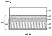
図8Aは干渉変調器(IMOD)811を含む干渉表示装置800の実施形態の断面図である。IMOD811は基板層801に隣接して配置することができる。基板801はどのような好適な基板からなるものであってもよく、例えば、アクリル、ガラス、ポリエチレンテレフタラート(PET)及び/またはポリエチレンテレフタラートグリコール(PET‐G)からなるものであってもよい。IMOD811は、吸収層803、反射層809、及び吸収層803と反射層809の間に画定される光学共振キャビティ層821を含んでもよい。反射層809は、空隙807を通して吸収層に対して略垂直な方向に、(図に示された)開状態と図1を参照して説明した閉状態との間を動くことができる。干渉変調器811は、基板801側から一人またはそれ以上の観察者の方向へ、反射層801が開状態の時には例えば赤、緑または青の色を反射するように構成され、反射層が作動状態の時には例えば黒や濃い青のような暗い色を反射するように構成されてもよい。
FIG. 8A is a cross-sectional view of an embodiment of an
図8Aに示す実施形態において、吸収層803は光学共振キャビティ821の上端となり、反射層809は光学共振キャビティ821の下端となる。吸収層803及び反射層809の厚さは、干渉反射体811によって反射される光と干渉反射体811を通して透過される光の相対量を制御するように選択することができる。吸収層803の厚さは、約40Åから約500Åの間の範囲とすることができる。反射層809の厚さは、約40Åから約500Åの間の範囲とすることができる。ある実施形態において、吸収層803及び反射層809は反射性かつ導電性である材料からなるものであってよい。吸収層803及び反射層809はともに金属からなるものであってもよく、ともに部分的に透過性であってもよい。吸収層803は様々な材料からなるものであってもよく、例えばモリブデン(Mo)、チタン(Ti)、タングステン(W)、及びクロム(Cr)からなってもよい。また同様に例えばMoCrやPbSeのような合金であってもよい。反射層809は様々な材料からなるものであってもよく、例えば、アルミニウム(Al)、銅(Cu)、銀(Ag)、モリブデン(Mo)、金(Au)及びクロム(Cr)からなってもよく、同様に例えばMoCrのような合金からなるものであってもよい。
In the embodiment shown in FIG. 8A, the
反射層809によって反射されまたは透過する光の量は、反射層809の厚さ及び組成を変更することにより、顕著に増加させまたは減少させることができる。干渉変調器から反射された光の結果的な色は、光学共振キャビティ821の大きさ(例えば、厚さ)及び吸収層803の材料特性に影響される光の干渉原理に基づく。反射層809の厚さを変更すると、反射された色の強度に影響し、反射層809を通した透過光の強度に影響を与える。
The amount of light reflected or transmitted by the
IMODの幾つかの実施形態においては、光学共振キャビティ821は固体の層、例えば、光学的に透明な単一の絶縁層(例えば、SiON)または複数の層によって画定される。他のIMODにおいては、光学共振キャビティ821は空隙、または光学的に透明な層805と空隙807との組み合わせによって画定される。光学共振キャビティ821の厚さはIMODからの一つまたはそれ以上の特定の色の反射を最大化または最小化するように調整することができる。ある実施形態においては、光学共振キャビティ821の厚さは約1000Åから約5000Åの範囲とすることができ、さらに厚くてもよい。光学共振キャビティ821の物理的な厚さは、それを形成する材料に依存しうる。例えば、SiONは空気よりも大きな屈折率を持つため、等価な光学的厚さとすると、空隙はSiONからなるキャビティよりも物理的に厚くなる。ある実施形態においては、光学共振キャビティ821の構成された厚さはキャビティ821の光学的厚さに基づいて選択することができる。ここで用いられるように、「光学的厚さ」は、IMOD811からの反射ピークの波長において測定されたキャビティ821の等価光学経路長を示している。すなわち、実際の物理的な距離はIMOD811の設計と選択される材料の双方に依存して顕著に変化し得るため、キャビティ821の設計は、光学的厚さ(例えば、波数)として表せば便利である。ある実施形態において、光学共振キャビティ821の光学的厚さはIMOD811の反射ピーク波長の約1/4から約10倍の範囲であってよい。従って、IMODによって反射される単一の色(または複数の色)は、光学共振キャビティ821がある特定の厚さを有するように構成することで選択することができる。
In some embodiments of the IMOD, the optical
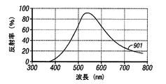
図8Bは、反射層が開状態(または非作動状態)のときの図8Aに示されるように構成された干渉変調器の基板側から反射される光の反射曲線901を示す概略図である。干渉変調器は、約50Åの厚さの吸収層と、約2440Åの厚さの光学共振キャビティと、約300Åの厚さの反射層と、を含む。図8Bに示すように、この特定の干渉変調器の反射ピークは、約540nmの波長において約90%である。従って、干渉変調器は反射層が開状態にあるときには、変調器の基板側から緑の光を反射するように調整されている。上述のように、干渉変調器は作動時には暗くなる。干渉変調器の基板側から反射された光の反射ピーク及び波長は、吸収層、光学共振キャビティ及び/または反射層を調整することによって変化させることができる。例えば、反射体が開位置にあるときに、干渉変調器が他の色を反射するように構成してもよい。
FIG. 8B is a schematic diagram showing a
図9Aは、他の一実施形態の干渉表示装置800の一部を表す断面図である。図9Aは図8Aに示される反射層809ではなく、干渉反射体813を含む。干渉反射体813は、観察者に向かって反射する光のスペクトルにさまざまなスペクトル幅、位置または強度を備えた凹みとなる透過ピークを導入するように調整することができる。したがって、ここで用いられているような「干渉反射体」という語句は、それ自身の上で光のある特定の波長を選択的に透過し反射する要素を表し、干渉表示装置においては、全体として表示装置から光のある特定の波長を選択的に反射し透過するように用いることができる。ある実施形態において、干渉反射体813はエタロンの共振に対応する透過ピークを示しうるファブリー・ペロー・エタロンまたはエタロン反射体と類似してもよい。
FIG. 9A is a cross-sectional view illustrating a part of an
干渉反射体813は、上面反射層815と、下面反射層819と、上面反射層と下面反射層との間に配置された光学共振層817とを含む。干渉反射体813によって導入される透過ピークは光学共振層の厚さまたは屈折率を変化させることにより及び/または上面反射層815及び下面反射層819の反射率を変化させることにより選択可能(調整可能)である。上面反射層815及び下面反射層819の反射率は、各層の厚さ及び/または各層を形成する材料の選択により影響を及ぼすことができる。
The
上面反射層815及び下面反射層819は共に金属からなるものであってもよく、共に部分的に透過性となるように構成されてもよい。反射層815、819は、例えば、アルミニウム(Al)、銀(Ag)、モリブデン(Mo)、金(Au)及び/またはクロム(Cr)からなるものであってもよく、また同様に例えばMoCrのような合金からなるものであってもよい。反射層815、819は同じ材料から形成されてもよく、異なる材料から形成されてもよい。例えば、上面反射層815はアルミニウムからなり、下面反射層はアルミニウムからなるものであってもよい。
Both the upper
上面反射層815及び下面反射層819の厚さは、好適な反射率および透過率特性に依存して変化しうる。ある実施形態において、上面反射層815の厚さは下面反射層819の厚さよりも薄い。他の実施形態においては、上面反射層815の厚さは下面反射層819の厚さと略同じである。上面反射層815及び下面反射層819の厚さは、約5Åから約1200Åの範囲であってよい。例えば、上面反射層は約120Åであってもよく、下面反射層は約600Åであってもよい。
The thickness of the top
光学共振層817は一つまたはそれ以上の光学共振材料から形成される。好適な光学共振材料の例は、空気や光学的に透明な絶縁体(例えば、SiON)を含む。光学共振層817は、単一の層あるいは複数の層から形成されてもよい。一実施形態において、光学共振層817はSiONの単一の層からなる。他の一実施形態において、光学共振層817は空気からなる。また他の一実施形態において、光学共振層817は一つまたはそれ以上の空気及び透明な絶縁体からなる層からなる。
The optical
光学共振層817が空気の層からなるような実施形態において、上面反射層815及び下面反射層819は、一方からの距離が固定された状態のままであってもよく、一方に対して相対的に動くものであってもよい。例えば、干渉反射体813は空気からなる光学共振層817を含んでもよく、下面反射層819は上面反射層815に対して動き、下面反射層が動作することにより光学共振層の厚さを変化させてもよい。上面反射層815と下面反射層819の間の距離によって画定される光学共振層817の厚さは以下により詳細に説明するように、透過ピークの位置または透過ピークの次数を調整するように調整されてもよい。従って、干渉反射体813は、上面反射層815と下面反射層819の間の距離が変わることにより時間の経過とともに変化する一つまたはそれ以上の透過ピークを導入するように構成されてもよい。
In an embodiment in which the optical
図9Bは開状態にある干渉反射体を含む干渉変調器の基板側から反射する光の反射率曲線903を示す図である。この例では、干渉反射体は約30Åの厚さを有するアルミニウムからなる第一の反射層と、約1300Åの厚さを有するSiONからなる光学共振層と、約30Åの厚さを有するアルミニウムからなる第二の反射層とを含む。
FIG. 9B is a diagram showing a
図9Bに示すように、光の反射率曲線903は干渉反射体によって導入された透過ピークによる約520nmの波長の部分にある凹み907を含む。この反射率の凹み907は、反射体内に光学共振層を含まず、従って反射率の凹みを導入しない反射体を用いる干渉変調器からの光と比較して、反射した光903の見え方を変化させる。干渉反射体によって生成された透過ピークがより広い範囲の波長に渡って反射率を「平らにする」ため、図9Bの反射された光は、観察者にとって図9Aの反射された光よりも異なって見える。
As shown in FIG. 9B, the
図9Cは開状態にある干渉反射体を含む干渉変調器の基板側から反射する光の反射率曲線905を示す図である。この例では、干渉反射体は約30Åの厚さを有するアルミニウムからなる第一の反射層と、約1300Åの厚さを有するSiONからなる光学共振層と、約30Åの厚さを有するアルミニウムからなる第二の反射層とを含む。光の反射曲線905は、干渉反射体によって導入された透過ピークによる約575nmの波長の部分にある凹み907を含む。干渉変調器の構成の違いにより、図9Bに示された計算による反射率の凹み907は、図9Cに示された測定された反射率の凹みとは異なる波長の部分にある。
FIG. 9C is a diagram showing a
図9Dはある特定の構成の干渉反射体を通した光の透過率曲線1003を示す。この例において、干渉反射体は約30Åの厚さを有するアルミニウムからなる第一の反射層と、約1300Åの厚さを有するSiONからなる光学共振層と、約30Åの厚さを有するアルミニウムからなる第二の反射層と、を備える。干渉反射体は、光学共振層の厚さに依存した複数の次数の透過ピーク909を導入するように構成されてもよい。より厚い光学共振層を備えた干渉反射体は、薄い光学共振層を備えた干渉反射体よりもより多くの次数の透過ピーク909を導入する。以下に説明するように、ピーク909の次数の調整に加えて、光学共振層の厚さはまた対応するピークの波長を調整するために変化させてもよい。
FIG. 9D shows a
図10Aは、干渉反射体を含む干渉変調器の基板側から反射する光の反射率曲線1001を示す図である。図10Aはまた、干渉変調器と干渉反射体の両方を通して伝搬する光の透過率曲線1003を示す。この例においては、図10Aに関する干渉変調器は約50Åの厚さを有する吸収層と約2440Åの厚さを有する光学共振キャビティとを含む。干渉反射体は約30Åの厚さを有するアルミニウムからなる第一の反射層と、約1300Åの厚さを有するSiONからなる光学共振層と、約30Åの厚さを有するアルミニウムからなる第二の反射層とを含む。光の反射率曲線1001は、約520nmの波長の位置に凹み907を含む。光の透過率曲線1003は約520nmの波長の位置にピーク909を含む。透過ピーク909は干渉反射体を通り、干渉変調器に入射する光の約1%の透過率となる。この光は観察者の方に反射して戻らないので失われるが、そのような光の損失は装置の反射率全体を顕著に減少させることはない。
FIG. 10A is a diagram showing a
干渉反射体を通した光の透過率は干渉変調器からの反射率全体を減少させるので、透過率ピーク909及び反射率の凹み907は一般に同じ波長の位置に配置される。しかしながら、透過率ピーク909の位置は反射率1001のスペクトルの位置に影響されない。すなわち、反射率曲線1001は干渉変調器の光学共振キャビティの厚さを変化させることによって調整することができるが、干渉反射体の構成による透過率ピーク907は同じ位置にとどまる。図10Bは、図10Bにおいて光学共振キャビティが減少させられたのを除けば、図10Aの状態を生成するのに用いられる干渉変調器と同一の干渉変調器の基板側から反射する光の反射率曲線1005を示す。図10Bはまた干渉反射体を通して伝搬した光の透過率曲線1003を示す。上述したように、干渉変調器からの光の反射率は光学共振キャビティの厚さを変化させることにより調整することができる。図10Bからわかるように、光学共振キャビティ層の厚さを減少させると、図10Aに示される反射率に対して、反射率曲線1005が変化する。しかしながら、干渉反射体は図10Aにみられるピークとほぼ同じピーク909を導入し、図10Bに示される透過率曲線1003は、図10Aに示される透過率曲線とほぼ同じである。従って、透過率ピーク909の位置及びそれに対応する反射率の凹み907は、光学共振キャビティが変化しても、変わることはない。
Since the transmittance of light through the interference reflector reduces the overall reflectance from the interferometric modulator, the
図10Cは、特定の干渉変調器、例えば、図10Aの状態を生成するのに用いられた干渉変調器のような干渉変調器の基板側から約30度の視野角で反射する光の反射率曲線1015を示す。図10Cはまた干渉反射体を通過する光の透過率曲線1013も示す。図10Cに示すように、透過率ピーク909とそれに対応する反射率の凹み907は共に、干渉変調器を異なる入射角から見ると、反射スペクトル全体とともにシフトする。
FIG. 10C shows the reflectivity of light reflected at a viewing angle of about 30 degrees from the substrate side of a particular interferometric modulator, eg, an interferometric modulator such as the interferometric modulator used to generate the state of FIG. 10A.
図11Aは、干渉反射体を含む干渉変調器の基板側から反射する光の反射率曲線1101を示す図である。図11Aはまた干渉反射体を通過する光の透過率曲線1103も示す。図11Aの状態を生成するのに用いられる干渉変調器は、約50Åの厚さである吸収層と、約2440Åの厚さである光学共振キャビティとを含む。干渉反射体は約15Åの厚さを有するアルミニウムからなる第一の反射層と、約1300Åの厚さを有するSiONからなる光学共振層と、約30Åの厚さを有するアルミニウムからなる第二の反射層と、を含む。光の反射率曲線1101は凹み907を含み、光の透過率曲線1103はピーク909を含む。
FIG. 11A is a diagram showing a
図10Aと図11Aとを比較すると、凹み907の大きさに対する第一の反射層の厚さの影響がわかる。第一の反射層が図10Aの状態を生成するのに用いられる干渉反射体のものよりも厚いため、図11Aに示される凹み907は図10Aに示される凹み907よりも大きい。第一の反射層の厚さは干渉変調器からの反射率全体に影響を及ぼす。第一の反射層が厚いと、干渉変調器から反射される光はより多くなり、第一の反射層が薄いと反射される光は少なくなる。
Comparing FIG. 10A and FIG. 11A, the influence of the thickness of the first reflective layer on the size of the
同様に、第二の反射層の厚さは干渉変調器及び干渉反射体を通した透過率全体に影響する。図11Bは、干渉反射体を含むある特定の干渉変調器の基板側から反射する光の反射率曲線1105を示す図である。図11Bはまた干渉反射体を通った光の透過率曲線1107も示す。図11Bに関する干渉変調器は約50Åの厚さの吸収層と、約2440Åの厚さの光学共振キャビティとを含む。干渉反射体は、約30Åの厚さを有するアルミニウムからなる第一の反射層と、約1300Åの厚さを有するSiONからなる光学共振層と、約15Åの厚さを有するアルミニウムからなる第二の反射層と、を含む。光の反射率曲線1105は、反射した光のスペクトルに凹み907を含み、光の透過率曲線1107はピーク909を含む。
Similarly, the thickness of the second reflective layer affects the overall transmission through the interferometric modulator and interference reflector. FIG. 11B is a diagram showing a
図10Aと図11Bとを比較すると、ピーク909の強度に対する第二の反射層の厚さの効果がわかる。第二の反射層が図10Aの状態を生成するのに用いられた干渉反射体の第二の反射層よりも厚いため、図11Bのピーク909は図10Aのピーク909よりも大きな強度を有する。第二の反射層の厚さは干渉変調器からの透過率全体に影響を及ぼし、第二の反射層が厚くなると透過光は少なくなり、第二の反射層が薄くなると透過光は多くなる。従って、干渉反射体における反射層の厚さを調整すれば、干渉変調器からの反射率全体及び干渉反射体を通る透過率全体を調整することができる。
Comparing FIG. 10A and FIG. 11B shows the effect of the thickness of the second reflective layer on the intensity of
図12Aは、干渉反射体を含むある干渉変調器の基板側から反射する光の反射率曲線1203を示す図である。図12Aはまた干渉反射体を透過する光の透過率曲線1205も示す。この例では、図12Aの状態を生成するのに用いられた干渉変調器は、約50Åの厚さの吸収層と、約2440Åの厚さの光学共振キャビティとを含む。干渉反射体は約270Åの厚さを有するアルミニウムからなる第一の反射層と、約1300Åの厚さを有するSiONからなる光学共振層と、約300Åの厚さを有するアルミニウムからなる第二の反射層と、を含む。光の反射率曲線1203は、反射率の凹み907を含み、光の透過率曲線1205はピーク909を含む。この例では、凹み907とピーク909は約520nmの波長の位置にほぼ位置し、ピーク909の強度全体は約0.4%である。
FIG. 12A is a diagram showing a
図12Bは干渉反射体を含むある干渉変調器の基板側から反射する光の反射率曲線1207を示す図である。図12Bはまた干渉反射体を通過する光の透過率曲線1209も示す。この例では、干渉変調器は約50Åの厚さの吸収層と、約2440Åの厚さの光学共振キャビティと、を含む。干渉反射体は約270Åの厚さを有するアルミニウムからなる第一の反射層と、約2100Åの厚さを有するSiONからなる光学共振層と、約300Åの厚さを有するアルミニウムからなる第二の反射層と、を含む。光の透過率曲線1209は約390nmの波長に位置するピーク909を含む。ピーク909はまた光の反射率曲線1207の約390nmの波長の位置に凹みを導入する。しかしながら、約390nmの波長の反射率は5%未満であるため、反射率1207の凹みは顕著でない。
FIG. 12B is a diagram showing a
図12Aと図12Bとを比較すると、ピーク909の位置に対する光学共振層の厚さの効果がわかる。上述したように、ピークの位置及び/またはピークの次数は、干渉反射体に含まれる光学共振層の厚さを調整することによって変更できる。従って、光学共振層の厚さは、複数の分離した干渉変調器を含む干渉表示装置の全範囲を増加させるように選択することができる。
12A and 12B, the effect of the thickness of the optical resonance layer on the position of the
図13Aは開位置(または緩和位置)にある干渉反射体を含む干渉変調器の一実施形態の基板側から反射する光の反射率曲線1301を示す図である。図13Aはまた干渉反射体を通過する光の透過率曲線1303も示す。この干渉変調器は約40Åの厚さのMoCrからなる吸収層と、約1940Åの厚さの光学共振キャビティとを含む。干渉反射体は約120Åの厚さを有するアルミニウムからなる第一の反射面と、約2840Åの厚さを有するSiONからなる光学共振層と、約600Åの厚さを有するアルミニウムからなる第二の反射面とを含む。光の透過率曲線1303は約520nmの波長に位置するピーク909を含み、光の反射率曲線1301のほぼ同じ波長位置に凹み907を導入する。
FIG. 13A is a diagram showing a
干渉表示装置から反射される色の範囲を増加するよう追加的に、個々の干渉変調器から反射される色を変えるように干渉反射体が用いられてもよい。干渉反射体は反射する色を変えるのに十分な反射率の凹み907を導入するので、以下の表1に示すように、干渉反射体が緩和位置にいるときには、図13Aの状態を生成するのに用いられた干渉変調器は白色を表示する。つまり、標準の反射体はある特定の波長で選択的に反射及び透過をしないので、通常の反射体を干渉変調器で用いられる干渉反射体に置き換えると、白色ではなく異なる色が反射される。
In addition, interference reflectors may be used to change the color reflected from the individual interferometric modulators to increase the range of colors reflected from the interferometric display. Since the interference reflector introduces a

図13Bは、干渉反射体が作動位置にあるときの図13Aの状態を生成するために用いられた干渉変調器の基板側から反射する光の反射率曲線1305を示す図である。干渉反射体を作動させまたは吸収層の方へ移動させると、干渉変調器からの反射率1305全体が減少する。可視光1305はほとんど反射されないので、干渉変調器は暗い外観を呈する。図13Aと図13Bを比較すると、図13Bよりも図13Aの方が非常に多くの光が反射されるので、作動位置にある干渉反射体と開位置(緩和位置)にある干渉反射体との間でよいコントラスト比を得られる。反射率曲線1305は、凹み907を導入する透過率ピーク909とほぼ同じ位置にある凹み907を含む。下記の表2は図13Bの干渉変調器から反射される色の色座標を示す。
FIG. 13B is a diagram illustrating a
上述したように、光の透過率曲線1303は反射体の作動及び光学共振キャビティの厚さの変化に影響されないが、反射率曲線1305は干渉反射体、吸収層、及び/または光学共振キャビティを調整することにより影響を受ける。図14Aは開位置(または緩和位置)にある干渉反射体を含む干渉変調器の基板側から反射する光の反射率曲線1401を示す図である。図14Aはまた干渉反射体を通過する光の透過率曲線1403も示す。干渉変調器は約40Åの厚さのPbSeからなる吸収層と、約1940Åの厚さの光学共振キャビティ層とを含む。干渉反射体は図13Aの状態を生成するのに用いられた干渉反射体と同一である。透過率曲線1403は約520nmの波長に位置するピーク909を含み、反射率曲線1401のほぼ同じ波長の位置に凹み907を導入する。
As described above, the
図13Aと図14Aとを比較すると、吸収層の材料を変更しても、干渉反射体を通過する光の透過率には影響しないことがわかる。しかしながら、吸収層の材料の変更は干渉変調器からの光の反射率に影響を及ぼす。従って、吸収層、光学共振キャビティ及び干渉反射体は、干渉変調器から反射される色全体を変更するためにすべて調整され得る。下記の表3は、干渉変調器が開位置にあるときの図14Aの状態を生成するのに用いられた干渉変調器から反射される色の色座標を示す。図14Aの干渉変調器から反射される色は図13Aの干渉変調器から反射される色よりも白色に近い。 Comparing FIG. 13A and FIG. 14A, it can be seen that changing the material of the absorption layer does not affect the transmittance of light passing through the interference reflector. However, changing the material of the absorbing layer affects the reflectivity of light from the interferometric modulator. Thus, the absorbing layer, the optical resonant cavity, and the interference reflector can all be adjusted to change the overall color reflected from the interferometric modulator. Table 3 below shows the color coordinates of the colors reflected from the interferometric modulator used to generate the state of FIG. 14A when the interferometric modulator is in the open position. The color reflected from the interferometric modulator of FIG. 14A is closer to white than the color reflected from the interferometric modulator of FIG. 13A.
図14Bは、干渉反射体が作動位置にある図14Aの状態を生成するのに用いられた干渉変調器の基板側から反射する光の反射率曲線1405を示す図である。干渉反射体が作動すると干渉変調器からの反射率1405全体が減少し、作動位置と緩和位置の間の反射された光のコントラストにより干渉変調器は暗い外観を呈する。下記の表4は図14Bの干渉変調器から反射された色の色座標を示す。
FIG. 14B shows a
以上、本発明の特定の実施形態について、詳細を説明した。しかしながら、上記の詳細な記載によらず、さまざまな方法で本発明は実施できることが理解されるであろう。また、上述のように、本発明の特定の特徴や側面を記載する際の特定の専門用語の使用は、その専門用語が、その専門用語が係る発明の特徴や側面のあらゆる特定の特性を含むように限定されてここで再定義されていることを意味すると解釈されるべきではない。それゆえ、本発明の範囲は、特許請求の範囲及びその同等物によって解釈されるべきである。 The details of the specific embodiments of the present invention have been described above. However, it will be understood that the invention can be practiced in a variety of ways, regardless of the above detailed description. Also, as noted above, the use of a particular terminology when describing a particular feature or aspect of the present invention includes that particular terminology includes any particular characteristic of the feature or aspect of the invention to which the terminology pertains. It should not be construed to mean so limited and redefined herein. Therefore, the scope of the invention should be construed by the claims and their equivalents.
12a、12b 干渉変調器
14a、14b 可動反射層
16a、16b 光学積層体
18 ポスト
19 ギャップ
20 基板
21 プロセッサ
22 アレイドライバ
24 行駆動回路
26 列駆動回路
27 ネットワークインターフェース
28 フレームバッファ
29 ドライバコントローラ
30 表示部
32 紐状構造
34 変形可能な層
40 表示装置
41 筐体
42 支持柱プラグ
43 アンテナ
44 バス構造
45 スピーカー
46 マイク
47 送受信部
48 入力装置
50 電源部
52 調整用ハードウェア
800 干渉表示装置
801 基板
803 吸収層
805 透明層
807 空隙
809 反射層
811 干渉変調器(IMOD)
813 干渉反射体
815 上面反射層
817 光学共振層
819 下面反射層
903、905、1001、1005、1015、1101、1105、1203、1207、1301、1305、1401、1405 反射率曲線
907 反射率の凹み
909 透過率ピーク
1003、1013、1103、1107、1205、1209、1303、1403 透過率曲線
12a,
813
Claims (47)
第一の反射面と、
第二の反射面と、
前記第一の反射面及び前記第二の反射面によって画定される光学共振層と、を備える、請求項1に記載の干渉変調器。 The interference reflector is
A first reflective surface;
A second reflective surface;
The interferometric modulator of claim 1, comprising: an optical resonant layer defined by the first reflective surface and the second reflective surface.
前記吸収層に対して略垂直な方向に移動するように構成された干渉反射体であって、前記干渉反射体が前記吸収層と前記干渉反射体素子との間の少なくとも一部に位置する空気からなる可変な空隙を通して移動し、第一の反射層と、第二の反射層と、前記第一の反射層と前記第二の反射層との間に配置された光学共振層と、を備える干渉反射体と、を備え、
干渉表示装置が透過ピーク波長において光の反射率が減少するように、前記干渉反射体が透過ピーク波長において光の特定のスペクトルを透過するように構成された、干渉変調装置。 An absorbent layer;
An interference reflector configured to move in a direction substantially perpendicular to the absorption layer, wherein the interference reflector is located at least at a part between the absorption layer and the interference reflector element. And a first reflective layer, a second reflective layer, and an optical resonant layer disposed between the first reflective layer and the second reflective layer. An interference reflector,
An interference modulation device, wherein the interference reflector is configured to transmit a specific spectrum of light at the transmission peak wavelength so that the interference display device has a reduced light reflectance at the transmission peak wavelength.
前記表示装置と通信するように構成されたプロセッサであって、画像データを処理するように構成されたプロセッサと、
前記プロセッサと通信するように構成されたメモリ装置と、をさらに備えた、請求項27に記載の干渉変調装置。 A display device;
A processor configured to communicate with the display device, wherein the processor is configured to process image data;
28. The interferometric modulator of claim 27, further comprising a memory device configured to communicate with the processor.
干渉変調器が透過ピーク波長において光の反射率が減少するように、透過ピーク波長において光の特定のスペクトルを透過するように構成された干渉反射手段と、を備える干渉変調装置。 Absorption means;
An interference modulation device comprising: an interference reflection unit configured to transmit a specific spectrum of light at the transmission peak wavelength so that the interferometric modulator reduces light reflectance at the transmission peak wavelength.
第一の反射面と、
第二の反射面と、
前記第一の反射面と前記第二の反射面との間で画定された光学共振層と、を備えた、請求項44に記載の干渉変調装置。 The interference reflection means is
A first reflective surface;
A second reflective surface;
45. The interferometric modulator of claim 44, comprising an optical resonant layer defined between the first reflective surface and the second reflective surface.
干渉反射体を提供する段階と、
前記干渉反射体の少なくとも一部と前記吸収層の少なくとも一部との間に光学共振キャビティを設けるように前記干渉反射体を前記吸収層に対して位置させる段階と、を備える干渉変調装置の製造方法。 Providing an absorbent layer;
Providing an interference reflector;
Positioning the interference reflector relative to the absorption layer so as to provide an optical resonant cavity between at least a portion of the interference reflector and at least a portion of the absorption layer. Method.
Applications Claiming Priority (3)
| Application Number | Priority Date | Filing Date | Title |
|---|---|---|---|
| US12/568,472 | 2009-09-28 | ||
| US12/568,472 US8488228B2 (en) | 2009-09-28 | 2009-09-28 | Interferometric display with interferometric reflector |
| PCT/US2010/049851 WO2011038020A1 (en) | 2009-09-28 | 2010-09-22 | Interferometric display with interferometric reflector |
Publications (2)
| Publication Number | Publication Date |
|---|---|
| JP2013506160A true JP2013506160A (en) | 2013-02-21 |
| JP5499175B2 JP5499175B2 (en) | 2014-05-21 |
Family
ID=43299642
Family Applications (1)
| Application Number | Title | Priority Date | Filing Date |
|---|---|---|---|
| JP2012530998A Expired - Fee Related JP5499175B2 (en) | 2009-09-28 | 2010-09-22 | Interference display device with interference reflector |
Country Status (6)
| Country | Link |
|---|---|
| US (2) | US8488228B2 (en) |
| EP (1) | EP2483733A1 (en) |
| JP (1) | JP5499175B2 (en) |
| KR (1) | KR20120081169A (en) |
| CN (1) | CN102576150A (en) |
| WO (1) | WO2011038020A1 (en) |
Families Citing this family (17)
| Publication number | Priority date | Publication date | Assignee | Title |
|---|---|---|---|---|
| US7527998B2 (en) | 2006-06-30 | 2009-05-05 | Qualcomm Mems Technologies, Inc. | Method of manufacturing MEMS devices providing air gap control |
| US8488228B2 (en) * | 2009-09-28 | 2013-07-16 | Qualcomm Mems Technologies, Inc. | Interferometric display with interferometric reflector |
| KR20130100232A (en) | 2010-04-09 | 2013-09-10 | 퀄컴 엠이엠에스 테크놀로지스, 인크. | Mechanical layer of an electromechanical device and methods of forming the same |
| CN103109315A (en) | 2010-08-17 | 2013-05-15 | 高通Mems科技公司 | Actuation and calibration of a charge neutral electrode in an interferometric display device |
| US9057872B2 (en) | 2010-08-31 | 2015-06-16 | Qualcomm Mems Technologies, Inc. | Dielectric enhanced mirror for IMOD display |
| US8963159B2 (en) | 2011-04-04 | 2015-02-24 | Qualcomm Mems Technologies, Inc. | Pixel via and methods of forming the same |
| US9134527B2 (en) | 2011-04-04 | 2015-09-15 | Qualcomm Mems Technologies, Inc. | Pixel via and methods of forming the same |
| US8659816B2 (en) | 2011-04-25 | 2014-02-25 | Qualcomm Mems Technologies, Inc. | Mechanical layer and methods of making the same |
| US8643936B2 (en) * | 2011-05-04 | 2014-02-04 | Qualcomm Mems Technologies, Inc. | Devices and methods for achieving non-contacting white state in interferometric modulators |
| US8736939B2 (en) | 2011-11-04 | 2014-05-27 | Qualcomm Mems Technologies, Inc. | Matching layer thin-films for an electromechanical systems reflective display device |
| US8995043B2 (en) * | 2011-11-29 | 2015-03-31 | Qualcomm Mems Technologies, Inc. | Interferometric modulator with dual absorbing layers |
| US9619084B2 (en) * | 2012-10-04 | 2017-04-11 | Corning Incorporated | Touch screen systems and methods for sensing touch screen displacement |
| CN107664837A (en) * | 2017-10-20 | 2018-02-06 | 京东方科技集团股份有限公司 | A kind of reflective display |
| DE102017221232A1 (en) * | 2017-11-28 | 2019-05-29 | Continental Reifen Deutschland Gmbh | Sulfur crosslinkable rubber compound, vulcanizate of the rubber mixture and vehicle tires |
| CN108196362B (en) * | 2018-01-03 | 2020-06-12 | 京东方科技集团股份有限公司 | Pixel structure, pixel driving method, array substrate and display device |
| TWI780430B (en) * | 2020-05-07 | 2022-10-11 | 緯創資通股份有限公司 | Detection device and method thereof |
| TWI839728B (en) * | 2020-05-07 | 2024-04-21 | 緯創資通股份有限公司 | Detection device and method thereof |
Citations (6)
| Publication number | Priority date | Publication date | Assignee | Title |
|---|---|---|---|---|
| JPH01114802A (en) * | 1987-10-28 | 1989-05-08 | Toshiba Corp | Light interference film |
| JP2002040238A (en) * | 2000-07-19 | 2002-02-06 | Sony Corp | Optical multilayer structure, optical switching element, and image display device |
| JP2003029169A (en) * | 2001-07-12 | 2003-01-29 | Sony Corp | Optical multilayer structure, method of manufacturing the same, optical switching element and image display device |
| JP2007147833A (en) * | 2005-11-25 | 2007-06-14 | Okayama Prefecture | Optical switching device and image display device using optical switching device |
| JP2008176104A (en) * | 2007-01-19 | 2008-07-31 | Olympus Corp | Optical element, optical unit and optical apparatus |
| WO2009039003A2 (en) * | 2007-09-17 | 2009-03-26 | Qualcomm Mems Technologies, Inc. | Semi-transparent/ transflective lighted interferometric modulator devices |
Family Cites Families (316)
| Publication number | Priority date | Publication date | Assignee | Title |
|---|---|---|---|---|
| US1877512A (en) | 1929-02-21 | 1932-09-13 | Nat Paper Process Company | Method of producing normal light effects |
| US2590906A (en) | 1946-11-22 | 1952-04-01 | Farrand Optical Co Inc | Reflection interference filter |
| US2677714A (en) | 1951-09-21 | 1954-05-04 | Alois Vogt Dr | Optical-electrical conversion device comprising a light-permeable metal electrode |
| US3247392A (en) | 1961-05-17 | 1966-04-19 | Optical Coating Laboratory Inc | Optical coating and assembly used as a band pass interference filter reflecting in the ultraviolet and infrared |
| US3247382A (en) * | 1962-09-04 | 1966-04-19 | Western Electric Co | Methods of locating leaks in multijacketed cable sheaths with radioactive gases |
| US3728030A (en) | 1970-06-22 | 1973-04-17 | Cary Instruments | Polarization interferometer |
| US3679313A (en) | 1970-10-23 | 1972-07-25 | Bell Telephone Labor Inc | Dispersive element for optical pulse compression |
| JPS4946974A (en) | 1972-09-11 | 1974-05-07 | ||
| US3886310A (en) | 1973-08-22 | 1975-05-27 | Westinghouse Electric Corp | Electrostatically deflectable light valve with improved diffraction properties |
| JPS5690489U (en) * | 1979-12-14 | 1981-07-18 | ||
| NL8001281A (en) | 1980-03-04 | 1981-10-01 | Philips Nv | DISPLAY DEVICE. |
| DE3109653A1 (en) | 1980-03-31 | 1982-01-28 | Jenoptik Jena Gmbh, Ddr 6900 Jena | "RESONANCE ABSORBER" |
| US4421381A (en) | 1980-04-04 | 1983-12-20 | Yokogawa Hokushin Electric Corp. | Mechanical vibrating element |
| US4441791A (en) | 1980-09-02 | 1984-04-10 | Texas Instruments Incorporated | Deformable mirror light modulator |
| US4497974A (en) | 1982-11-22 | 1985-02-05 | Exxon Research & Engineering Co. | Realization of a thin film solar cell with a detached reflector |
| US4498953A (en) | 1983-07-27 | 1985-02-12 | At&T Bell Laboratories | Etching techniques |
| US5096279A (en) | 1984-08-31 | 1992-03-17 | Texas Instruments Incorporated | Spatial light modulator and method |
| US4560435A (en) | 1984-10-01 | 1985-12-24 | International Business Machines Corporation | Composite back-etch/lift-off stencil for proximity effect minimization |
| US4655554A (en) | 1985-03-06 | 1987-04-07 | The United States Of America As Represented By The Secretary Of The Air Force | Spatial light modulator having a capacitively coupled photoconductor |
| US4859060A (en) | 1985-11-26 | 1989-08-22 | 501 Sharp Kabushiki Kaisha | Variable interferometric device and a process for the production of the same |
| US4705361A (en) | 1985-11-27 | 1987-11-10 | Texas Instruments Incorporated | Spatial light modulator |
| GB8621438D0 (en) | 1986-09-05 | 1986-10-15 | Secr Defence | Electro-optic device |
| US4786128A (en) | 1986-12-02 | 1988-11-22 | Quantum Diagnostics, Ltd. | Device for modulating and reflecting electromagnetic radiation employing electro-optic layer having a variable index of refraction |
| US4822993A (en) | 1987-02-17 | 1989-04-18 | Optron Systems, Inc. | Low-cost, substantially cross-talk free high spatial resolution 2-D bistable light modulator |
| US5091983A (en) | 1987-06-04 | 1992-02-25 | Walter Lukosz | Optical modulation apparatus and measurement method |
| US4956619A (en) | 1988-02-19 | 1990-09-11 | Texas Instruments Incorporated | Spatial light modulator |
| US5028939A (en) | 1988-08-23 | 1991-07-02 | Texas Instruments Incorporated | Spatial light modulator system |
| US4925259A (en) | 1988-10-20 | 1990-05-15 | The United States Of America As Represented By The United States Department Of Energy | Multilayer optical dielectric coating |
| US4982184A (en) | 1989-01-03 | 1991-01-01 | General Electric Company | Electrocrystallochromic display and element |
| US4973131A (en) | 1989-02-03 | 1990-11-27 | Mcdonnell Douglas Corporation | Modulator mirror |
| US5022745A (en) | 1989-09-07 | 1991-06-11 | Massachusetts Institute Of Technology | Electrostatically deformable single crystal dielectrically coated mirror |
| US4954789A (en) | 1989-09-28 | 1990-09-04 | Texas Instruments Incorporated | Spatial light modulator |
| US5083857A (en) | 1990-06-29 | 1992-01-28 | Texas Instruments Incorporated | Multi-level deformable mirror device |
| US5062689A (en) | 1990-08-21 | 1991-11-05 | Koehler Dale R | Electrostatically actuatable light modulating device |
| US5287215A (en) | 1991-07-17 | 1994-02-15 | Optron Systems, Inc. | Membrane light modulation systems |
| US5170283A (en) | 1991-07-24 | 1992-12-08 | Northrop Corporation | Silicon spatial light modulator |
| US5240818A (en) | 1991-07-31 | 1993-08-31 | Texas Instruments Incorporated | Method for manufacturing a color filter for deformable mirror device |
| US5315370A (en) | 1991-10-23 | 1994-05-24 | Bulow Jeffrey A | Interferometric modulator for optical signal processing |
| US6381022B1 (en) | 1992-01-22 | 2002-04-30 | Northeastern University | Light modulating device |
| TW245772B (en) | 1992-05-19 | 1995-04-21 | Akzo Nv | |
| US5818095A (en) | 1992-08-11 | 1998-10-06 | Texas Instruments Incorporated | High-yield spatial light modulator with light blocking layer |
| FI96450C (en) | 1993-01-13 | 1996-06-25 | Vaisala Oy | Single-channel gas concentration measurement method and equipment |
| US7830587B2 (en) | 1993-03-17 | 2010-11-09 | Qualcomm Mems Technologies, Inc. | Method and device for modulating light with semiconductor substrate |
| US6674562B1 (en) | 1994-05-05 | 2004-01-06 | Iridigm Display Corporation | Interferometric modulation of radiation |
| US5559358A (en) | 1993-05-25 | 1996-09-24 | Honeywell Inc. | Opto-electro-mechanical device or filter, process for making, and sensors made therefrom |
| US5526172A (en) | 1993-07-27 | 1996-06-11 | Texas Instruments Incorporated | Microminiature, monolithic, variable electrical signal processor and apparatus including same |
| FI94804C (en) | 1994-02-17 | 1995-10-25 | Vaisala Oy | Electrically adjustable surface micromechanical Fabry-Perot interferometer for optical material analysis |
| US5665997A (en) | 1994-03-31 | 1997-09-09 | Texas Instruments Incorporated | Grated landing area to eliminate sticking of micro-mechanical devices |
| US7826120B2 (en) | 1994-05-05 | 2010-11-02 | Qualcomm Mems Technologies, Inc. | Method and device for multi-color interferometric modulation |
| US8081369B2 (en) | 1994-05-05 | 2011-12-20 | Qualcomm Mems Technologies, Inc. | System and method for a MEMS device |
| US20010003487A1 (en) | 1996-11-05 | 2001-06-14 | Mark W. Miles | Visible spectrum modulator arrays |
| US7738157B2 (en) | 1994-05-05 | 2010-06-15 | Qualcomm Mems Technologies, Inc. | System and method for a MEMS device |
| US6040937A (en) | 1994-05-05 | 2000-03-21 | Etalon, Inc. | Interferometric modulation |
| US6710908B2 (en) | 1994-05-05 | 2004-03-23 | Iridigm Display Corporation | Controlling micro-electro-mechanical cavities |
| US7852545B2 (en) | 1994-05-05 | 2010-12-14 | Qualcomm Mems Technologies, Inc. | Method and device for modulating light |
| US7550794B2 (en) | 2002-09-20 | 2009-06-23 | Idc, Llc | Micromechanical systems device comprising a displaceable electrode and a charge-trapping layer |
| US7123216B1 (en) | 1994-05-05 | 2006-10-17 | Idc, Llc | Photonic MEMS and structures |
| US7460291B2 (en) | 1994-05-05 | 2008-12-02 | Idc, Llc | Separable modulator |
| US6680792B2 (en) | 1994-05-05 | 2004-01-20 | Iridigm Display Corporation | Interferometric modulation of radiation |
| US7808694B2 (en) | 1994-05-05 | 2010-10-05 | Qualcomm Mems Technologies, Inc. | Method and device for modulating light |
| US5920418A (en) | 1994-06-21 | 1999-07-06 | Matsushita Electric Industrial Co., Ltd. | Diffractive optical modulator and method for producing the same, infrared sensor including such a diffractive optical modulator and method for producing the same, and display device including such a diffractive optical modulator |
| US5485304A (en) | 1994-07-29 | 1996-01-16 | Texas Instruments, Inc. | Support posts for micro-mechanical devices |
| US5636052A (en) | 1994-07-29 | 1997-06-03 | Lucent Technologies Inc. | Direct view display based on a micromechanical modulation |
| FR2726960B1 (en) | 1994-11-10 | 1996-12-13 | Thomson Csf | PROCESS FOR PRODUCING MAGNETORESISTIVE TRANSDUCERS |
| JPH08153700A (en) | 1994-11-25 | 1996-06-11 | Semiconductor Energy Lab Co Ltd | Method for anisotropically etching conductive coating |
| US5550373A (en) | 1994-12-30 | 1996-08-27 | Honeywell Inc. | Fabry-Perot micro filter-detector |
| US7898722B2 (en) | 1995-05-01 | 2011-03-01 | Qualcomm Mems Technologies, Inc. | Microelectromechanical device with restoring electrode |
| US5661592A (en) | 1995-06-07 | 1997-08-26 | Silicon Light Machines | Method of making and an apparatus for a flat diffraction grating light valve |
| US6849471B2 (en) | 2003-03-28 | 2005-02-01 | Reflectivity, Inc. | Barrier layers for microelectromechanical systems |
| US6046840A (en) | 1995-06-19 | 2000-04-04 | Reflectivity, Inc. | Double substrate reflective spatial light modulator with self-limiting micro-mechanical elements |
| US6124851A (en) | 1995-07-20 | 2000-09-26 | E Ink Corporation | Electronic book with multiple page displays |
| KR100213026B1 (en) | 1995-07-27 | 1999-08-02 | 윤종용 | Dmd and fabrication method for dmd |
| US6324192B1 (en) | 1995-09-29 | 2001-11-27 | Coretek, Inc. | Electrically tunable fabry-perot structure utilizing a deformable multi-layer mirror and method of making the same |
| JPH09127551A (en) | 1995-10-31 | 1997-05-16 | Sharp Corp | Semiconductor device and active matrix substrate |
| US5999306A (en) | 1995-12-01 | 1999-12-07 | Seiko Epson Corporation | Method of manufacturing spatial light modulator and electronic device employing it |
| US5825528A (en) | 1995-12-26 | 1998-10-20 | Lucent Technologies Inc. | Phase-mismatched fabry-perot cavity micromechanical modulator |
| US5751469A (en) | 1996-02-01 | 1998-05-12 | Lucent Technologies Inc. | Method and apparatus for an improved micromechanical modulator |
| US6114862A (en) | 1996-02-14 | 2000-09-05 | Stmicroelectronics, Inc. | Capacitive distance sensor |
| US5710656A (en) | 1996-07-30 | 1998-01-20 | Lucent Technologies Inc. | Micromechanical optical modulator having a reduced-mass composite membrane |
| US5838484A (en) | 1996-08-19 | 1998-11-17 | Lucent Technologies Inc. | Micromechanical optical modulator with linear operating characteristic |
| GB9619781D0 (en) | 1996-09-23 | 1996-11-06 | Secr Defence | Multi layer interference coatings |
| US5771116A (en) | 1996-10-21 | 1998-06-23 | Texas Instruments Incorporated | Multiple bias level reset waveform for enhanced DMD control |
| US7830588B2 (en) | 1996-12-19 | 2010-11-09 | Qualcomm Mems Technologies, Inc. | Method of making a light modulating display device and associated transistor circuitry and structures thereof |
| US6028689A (en) | 1997-01-24 | 2000-02-22 | The United States Of America As Represented By The Secretary Of The Air Force | Multi-motion micromirror |
| US5786927A (en) | 1997-03-12 | 1998-07-28 | Lucent Technologies Inc. | Gas-damped micromechanical structure |
| US6384952B1 (en) | 1997-03-27 | 2002-05-07 | Mems Optical Inc. | Vertical comb drive actuated deformable mirror device and method |
| EP0879991A3 (en) | 1997-05-13 | 1999-04-21 | Matsushita Electric Industrial Co., Ltd. | Illuminating system |
| US5870221A (en) | 1997-07-25 | 1999-02-09 | Lucent Technologies, Inc. | Micromechanical modulator having enhanced performance |
| US5867302A (en) | 1997-08-07 | 1999-02-02 | Sandia Corporation | Bistable microelectromechanical actuator |
| US6031653A (en) * | 1997-08-28 | 2000-02-29 | California Institute Of Technology | Low-cost thin-metal-film interference filters |
| DE69830153T2 (en) | 1998-01-20 | 2005-10-13 | Seiko Epson Corp. | OPTICAL SWITCHING DEVICE AND PICTURE DISPLAY |
| US5914804A (en) | 1998-01-28 | 1999-06-22 | Lucent Technologies Inc | Double-cavity micromechanical optical modulator with plural multilayer mirrors |
| US6100861A (en) | 1998-02-17 | 2000-08-08 | Rainbow Displays, Inc. | Tiled flat panel display with improved color gamut |
| US6262697B1 (en) | 1998-03-20 | 2001-07-17 | Eastman Kodak Company | Display having viewable and conductive images |
| WO1999052006A2 (en) | 1998-04-08 | 1999-10-14 | Etalon, Inc. | Interferometric modulation of radiation |
| US7532377B2 (en) | 1998-04-08 | 2009-05-12 | Idc, Llc | Movable micro-electromechanical device |
| US8928967B2 (en) | 1998-04-08 | 2015-01-06 | Qualcomm Mems Technologies, Inc. | Method and device for modulating light |
| US6046659A (en) | 1998-05-15 | 2000-04-04 | Hughes Electronics Corporation | Design and fabrication of broadband surface-micromachined micro-electro-mechanical switches for microwave and millimeter-wave applications |
| US6242989B1 (en) | 1998-09-12 | 2001-06-05 | Agere Systems Guardian Corp. | Article comprising a multi-port variable capacitor |
| US6323834B1 (en) | 1998-10-08 | 2001-11-27 | International Business Machines Corporation | Micromechanical displays and fabrication method |
| JP3919954B2 (en) | 1998-10-16 | 2007-05-30 | 富士フイルム株式会社 | Array type light modulation element and flat display driving method |
| JP2000147262A (en) | 1998-11-11 | 2000-05-26 | Nobuyuki Higuchi | Converging device and photovoltaic power generation system utilizing the device |
| US6188519B1 (en) | 1999-01-05 | 2001-02-13 | Kenneth Carlisle Johnson | Bigrating light valve |
| US6242932B1 (en) | 1999-02-19 | 2001-06-05 | Micron Technology, Inc. | Interposer for semiconductor components having contact balls |
| US6323987B1 (en) | 1999-05-14 | 2001-11-27 | Agere Systems Optoelectronics Guardian Corp. | Controlled multi-wavelength etalon |
| US6335235B1 (en) | 1999-08-17 | 2002-01-01 | Advanced Micro Devices, Inc. | Simplified method of patterning field dielectric regions in a semiconductor device |
| WO2003007049A1 (en) | 1999-10-05 | 2003-01-23 | Iridigm Display Corporation | Photonic mems and structures |
| US6351329B1 (en) | 1999-10-08 | 2002-02-26 | Lucent Technologies Inc. | Optical attenuator |
| US6960305B2 (en) | 1999-10-26 | 2005-11-01 | Reflectivity, Inc | Methods for forming and releasing microelectromechanical structures |
| US6519073B1 (en) | 2000-01-10 | 2003-02-11 | Lucent Technologies Inc. | Micromechanical modulator and methods for fabricating the same |
| JP2003520986A (en) | 2000-01-21 | 2003-07-08 | フレックス プロダクツ インコーポレイテッド | Optical modulation security device |
| US6307663B1 (en) | 2000-01-26 | 2001-10-23 | Eastman Kodak Company | Spatial light modulator with conformal grating device |
| GB2359636B (en) | 2000-02-22 | 2002-05-01 | Marconi Comm Ltd | Wavelength selective optical filter |
| JP2003524215A (en) | 2000-02-24 | 2003-08-12 | コーニンクレッカ フィリップス エレクトロニクス エヌ ヴィ | Display device with optical waveguide |
| US6836366B1 (en) | 2000-03-03 | 2004-12-28 | Axsun Technologies, Inc. | Integrated tunable fabry-perot filter and method of making same |
| US6747775B2 (en) | 2000-03-20 | 2004-06-08 | Np Photonics, Inc. | Detunable Fabry-Perot interferometer and an add/drop multiplexer using the same |
| US6698295B1 (en) | 2000-03-31 | 2004-03-02 | Shipley Company, L.L.C. | Microstructures comprising silicon nitride layer and thin conductive polysilicon layer |
| US6400738B1 (en) | 2000-04-14 | 2002-06-04 | Agilent Technologies, Inc. | Tunable Fabry-Perot filters and lasers |
| FR2811139B1 (en) | 2000-06-29 | 2003-10-17 | Centre Nat Rech Scient | OPTOELECTRONIC DEVICE WITH INTEGRATED WAVELENGTH FILTERING |
| KR100840827B1 (en) | 2000-07-03 | 2008-06-23 | 소니 가부시끼 가이샤 | Optical multilayer structures, optical switching devices and image displays |
| US6466354B1 (en) | 2000-09-19 | 2002-10-15 | Silicon Light Machines | Method and apparatus for interferometric modulation of light |
| US6714565B1 (en) | 2000-11-01 | 2004-03-30 | Agilent Technologies, Inc. | Optically tunable Fabry Perot microelectromechanical resonator |
| US6556338B2 (en) | 2000-11-03 | 2003-04-29 | Intpax, Inc. | MEMS based variable optical attenuator (MBVOA) |
| US6433917B1 (en) | 2000-11-22 | 2002-08-13 | Ball Semiconductor, Inc. | Light modulation device and system |
| US6906847B2 (en) | 2000-12-07 | 2005-06-14 | Reflectivity, Inc | Spatial light modulators with light blocking/absorbing areas |
| US6614576B2 (en) | 2000-12-15 | 2003-09-02 | Texas Instruments Incorporated | Surface micro-planarization for enhanced optical efficiency and pixel performance in SLM devices |
| US20020149834A1 (en) | 2000-12-22 | 2002-10-17 | Ball Semiconductor, Inc. | Light modulation device and system |
| DE10064616C2 (en) | 2000-12-22 | 2003-02-06 | Ovd Kinegram Ag Zug | Decorative film and method for labeling the decorative film |
| US6912078B2 (en) | 2001-03-16 | 2005-06-28 | Corning Incorporated | Electrostatically actuated micro-electro-mechanical devices and method of manufacture |
| US6661561B2 (en) | 2001-03-26 | 2003-12-09 | Creo Inc. | High frequency deformable mirror device |
| US6600587B2 (en) | 2001-04-23 | 2003-07-29 | Memx, Inc. | Surface micromachined optical system with reinforced mirror microstructure |
| US6657832B2 (en) | 2001-04-26 | 2003-12-02 | Texas Instruments Incorporated | Mechanically assisted restoring force support for micromachined membranes |
| WO2002095800A2 (en) | 2001-05-22 | 2002-11-28 | Reflectivity, Inc. | A method for making a micromechanical device by removing a sacrificial layer with multiple sequential etchants |
| JP3740444B2 (en) | 2001-07-11 | 2006-02-01 | キヤノン株式会社 | Optical deflector, optical equipment using the same, torsional oscillator |
| US6594059B2 (en) | 2001-07-16 | 2003-07-15 | Axsun Technologies, Inc. | Tilt mirror fabry-perot filter system, fabrication process therefor, and method of operation thereof |
| US6632698B2 (en) | 2001-08-07 | 2003-10-14 | Hewlett-Packard Development Company, L.P. | Microelectromechanical device having a stiffened support beam, and methods of forming stiffened support beams in MEMS |
| US6661562B2 (en) | 2001-08-17 | 2003-12-09 | Lucent Technologies Inc. | Optical modulator and method of manufacture thereof |
| US7015457B2 (en) | 2002-03-18 | 2006-03-21 | Honeywell International Inc. | Spectrally tunable detector |
| US20030053078A1 (en) | 2001-09-17 | 2003-03-20 | Mark Missey | Microelectromechanical tunable fabry-perot wavelength monitor with thermal actuators |
| ATE417021T1 (en) | 2001-11-09 | 2008-12-15 | Wispry Inc | THREE-LAYER BEAM MEMS DEVICE AND RELATED METHOD |
| US6761950B2 (en) | 2001-12-07 | 2004-07-13 | Matsushita Electric Industrial Co., Ltd. | Information recording medium and method for producing the same |
| JP2003177336A (en) | 2001-12-11 | 2003-06-27 | Fuji Photo Film Co Ltd | Optical modulating element, optical modulating element array, and exposure device using the same |
| US6791735B2 (en) | 2002-01-09 | 2004-09-14 | The Regents Of The University Of California | Differentially-driven MEMS spatial light modulator |
| US6608268B1 (en) | 2002-02-05 | 2003-08-19 | Memtronics, A Division Of Cogent Solutions, Inc. | Proximity micro-electro-mechanical system |
| US6794119B2 (en) | 2002-02-12 | 2004-09-21 | Iridigm Display Corporation | Method for fabricating a structure for a microelectromechanical systems (MEMS) device |
| US6574033B1 (en) | 2002-02-27 | 2003-06-03 | Iridigm Display Corporation | Microelectromechanical systems device and method for fabricating same |
| EP1482770A4 (en) | 2002-03-01 | 2007-01-03 | Sharp Kk | Light emitting device and display unit using the light emitting device and reading device |
| US7145143B2 (en) | 2002-03-18 | 2006-12-05 | Honeywell International Inc. | Tunable sensor |
| US6768555B2 (en) | 2002-03-21 | 2004-07-27 | Industrial Technology Research Institute | Fabry-Perot filter apparatus with enhanced optical discrimination |
| US6965468B2 (en) | 2003-07-03 | 2005-11-15 | Reflectivity, Inc | Micromirror array having reduced gap between adjacent micromirrors of the micromirror array |
| US6954297B2 (en) | 2002-04-30 | 2005-10-11 | Hewlett-Packard Development Company, L.P. | Micro-mirror device including dielectrophoretic liquid |
| US6972882B2 (en) | 2002-04-30 | 2005-12-06 | Hewlett-Packard Development Company, L.P. | Micro-mirror device with light angle amplification |
| JP3801099B2 (en) | 2002-06-04 | 2006-07-26 | 株式会社デンソー | Tunable filter, manufacturing method thereof, and optical switching device using the same |
| US6813059B2 (en) | 2002-06-28 | 2004-11-02 | Silicon Light Machines, Inc. | Reduced formation of asperities in contact micro-structures |
| US6738194B1 (en) | 2002-07-22 | 2004-05-18 | The United States Of America As Represented By The Secretary Of The Navy | Resonance tunable optical filter |
| US20040018599A1 (en) * | 2002-07-24 | 2004-01-29 | Rabinowitz Israel N. | Enhanced production from almond hulls of products such as inositol and inositol phosphates |
| US6822798B2 (en) | 2002-08-09 | 2004-11-23 | Optron Systems, Inc. | Tunable optical filter |
| EP1543370B1 (en) | 2002-09-19 | 2011-02-09 | Koninklijke Philips Electronics N.V. | Switchable optical element |
| JP4057871B2 (en) | 2002-09-19 | 2008-03-05 | 東芝松下ディスプレイテクノロジー株式会社 | Liquid crystal display |
| KR100512960B1 (en) | 2002-09-26 | 2005-09-07 | 삼성전자주식회사 | Flexible MEMS transducer and its manufacturing method, and flexible MEMS wireless microphone |
| US7085121B2 (en) | 2002-10-21 | 2006-08-01 | Hrl Laboratories, Llc | Variable capacitance membrane actuator for wide band tuning of microstrip resonators and filters |
| FR2846318B1 (en) | 2002-10-24 | 2005-01-07 | Commissariat Energie Atomique | INTEGRATED ELECTROMECHANICAL MICROSTRUCTURE HAVING MEANS FOR ADJUSTING THE PRESSURE IN A SEALED CAVITY AND A METHOD OF ADJUSTING THE PRESSURE |
| US7370185B2 (en) | 2003-04-30 | 2008-05-06 | Hewlett-Packard Development Company, L.P. | Self-packaged optical interference display device having anti-stiction bumps, integral micro-lens, and reflection-absorbing layers |
| US6844959B2 (en) | 2002-11-26 | 2005-01-18 | Reflectivity, Inc | Spatial light modulators with light absorbing areas |
| US6958846B2 (en) | 2002-11-26 | 2005-10-25 | Reflectivity, Inc | Spatial light modulators with light absorbing areas |
| TWI289708B (en) | 2002-12-25 | 2007-11-11 | Qualcomm Mems Technologies Inc | Optical interference type color display |
| TW594155B (en) | 2002-12-27 | 2004-06-21 | Prime View Int Corp Ltd | Optical interference type color display and optical interference modulator |
| JP2004219843A (en) | 2003-01-16 | 2004-08-05 | Seiko Epson Corp | Optical modulator, display device and manufacturing method thereof |
| TW557395B (en) | 2003-01-29 | 2003-10-11 | Yen Sun Technology Corp | Optical interference type reflection panel and the manufacturing method thereof |
| TW200413810A (en) | 2003-01-29 | 2004-08-01 | Prime View Int Co Ltd | Light interference display panel and its manufacturing method |
| US7436573B2 (en) | 2003-02-12 | 2008-10-14 | Texas Instruments Incorporated | Electrical connections in microelectromechanical devices |
| US7459402B2 (en) | 2003-02-12 | 2008-12-02 | Texas Instruments Incorporated | Protection layers in micromirror array devices |
| TW200417806A (en) | 2003-03-05 | 2004-09-16 | Prime View Int Corp Ltd | A structure of a light-incidence electrode of an optical interference display plate |
| US6913942B2 (en) | 2003-03-28 | 2005-07-05 | Reflectvity, Inc | Sacrificial layers for use in fabrications of microelectromechanical devices |
| TW594360B (en) | 2003-04-21 | 2004-06-21 | Prime View Int Corp Ltd | A method for fabricating an interference display cell |
| TWI224235B (en) | 2003-04-21 | 2004-11-21 | Prime View Int Co Ltd | A method for fabricating an interference display cell |
| TW567355B (en) | 2003-04-21 | 2003-12-21 | Prime View Int Co Ltd | An interference display cell and fabrication method thereof |
| TWI226504B (en) | 2003-04-21 | 2005-01-11 | Prime View Int Co Ltd | A structure of an interference display cell |
| US7447891B2 (en) | 2003-04-30 | 2008-11-04 | Hewlett-Packard Development Company, L.P. | Light modulator with concentric control-electrode structure |
| US7072093B2 (en) | 2003-04-30 | 2006-07-04 | Hewlett-Packard Development Company, L.P. | Optical interference pixel display with charge control |
| US6940630B2 (en) | 2003-05-01 | 2005-09-06 | University Of Florida Research Foundation, Inc. | Vertical displacement device |
| JP4075678B2 (en) | 2003-05-06 | 2008-04-16 | ソニー株式会社 | Solid-state image sensor |
| TW591716B (en) | 2003-05-26 | 2004-06-11 | Prime View Int Co Ltd | A structure of a structure release and manufacturing the same |
| TW570896B (en) | 2003-05-26 | 2004-01-11 | Prime View Int Co Ltd | A method for fabricating an interference display cell |
| TWI223855B (en) | 2003-06-09 | 2004-11-11 | Taiwan Semiconductor Mfg | Method for manufacturing reflective spatial light modulator mirror devices |
| JP2007027150A (en) | 2003-06-23 | 2007-02-01 | Hitachi Chem Co Ltd | Concentrating photovoltaic system |
| US7221495B2 (en) | 2003-06-24 | 2007-05-22 | Idc Llc | Thin film precursor stack for MEMS manufacturing |
| US6862127B1 (en) | 2003-11-01 | 2005-03-01 | Fusao Ishii | High performance micromirror arrays and methods of manufacturing the same |
| JP3786106B2 (en) | 2003-08-11 | 2006-06-14 | セイコーエプソン株式会社 | Wavelength tunable optical filter and manufacturing method thereof |
| TW200506479A (en) | 2003-08-15 | 2005-02-16 | Prime View Int Co Ltd | Color changeable pixel for an interference display |
| TWI251712B (en) | 2003-08-15 | 2006-03-21 | Prime View Int Corp Ltd | Interference display plate |
| TWI231865B (en) | 2003-08-26 | 2005-05-01 | Prime View Int Co Ltd | An interference display cell and fabrication method thereof |
| TWI230801B (en) | 2003-08-29 | 2005-04-11 | Prime View Int Co Ltd | Reflective display unit using interferometric modulation and manufacturing method thereof |
| JP3979982B2 (en) | 2003-08-29 | 2007-09-19 | シャープ株式会社 | Interferometric modulator and display device |
| TWI232333B (en) | 2003-09-03 | 2005-05-11 | Prime View Int Co Ltd | Display unit using interferometric modulation and manufacturing method thereof |
| US7027204B2 (en) | 2003-09-26 | 2006-04-11 | Silicon Light Machines Corporation | High-density spatial light modulator |
| US6982820B2 (en) | 2003-09-26 | 2006-01-03 | Prime View International Co., Ltd. | Color changeable pixel |
| TW593126B (en) | 2003-09-30 | 2004-06-21 | Prime View Int Co Ltd | A structure of a micro electro mechanical system and manufacturing the same |
| JP2005121906A (en) | 2003-10-16 | 2005-05-12 | Fuji Photo Film Co Ltd | Reflection type optical modulation array element and exposure device |
| US7782523B2 (en) | 2003-11-01 | 2010-08-24 | Fusao Ishii | Analog micromirror devices with continuous intermediate states |
| TW200524236A (en) | 2003-12-01 | 2005-07-16 | Nl Nanosemiconductor Gmbh | Optoelectronic device incorporating an interference filter |
| EP1544657B1 (en) | 2003-12-19 | 2012-04-04 | Barco N.V. | Broadband full white reflective display structure |
| WO2005089098A2 (en) | 2004-01-14 | 2005-09-29 | The Regents Of The University Of California | Ultra broadband mirror using subwavelength grating |
| TWI235345B (en) | 2004-01-20 | 2005-07-01 | Prime View Int Co Ltd | A structure of an optical interference display unit |
| US7342705B2 (en) | 2004-02-03 | 2008-03-11 | Idc, Llc | Spatial light modulator with integrated optical compensation structure |
| JP2005235403A (en) | 2004-02-17 | 2005-09-02 | Hitachi Displays Ltd | Organic EL display device |
| TWI256941B (en) | 2004-02-18 | 2006-06-21 | Qualcomm Mems Technologies Inc | A micro electro mechanical system display cell and method for fabricating thereof |
| US7119945B2 (en) | 2004-03-03 | 2006-10-10 | Idc, Llc | Altering temporal response of microelectromechanical elements |
| TW200530669A (en) | 2004-03-05 | 2005-09-16 | Prime View Int Co Ltd | Interference display plate and manufacturing method thereof |
| TWI261683B (en) | 2004-03-10 | 2006-09-11 | Qualcomm Mems Technologies Inc | Interference reflective element and repairing method thereof |
| JP4581453B2 (en) | 2004-03-29 | 2010-11-17 | ソニー株式会社 | MEMS element, optical MEMS element, diffractive optical MEMS element, and laser display |
| US7245285B2 (en) | 2004-04-28 | 2007-07-17 | Hewlett-Packard Development Company, L.P. | Pixel device |
| US7476327B2 (en) | 2004-05-04 | 2009-01-13 | Idc, Llc | Method of manufacture for microelectromechanical devices |
| US7787170B2 (en) | 2004-06-15 | 2010-08-31 | Texas Instruments Incorporated | Micromirror array assembly with in-array pillars |
| CA2572952C (en) | 2004-07-09 | 2012-12-04 | The University Of Cincinnati | Display capable electrowetting light valve |
| TWI233916B (en) | 2004-07-09 | 2005-06-11 | Prime View Int Co Ltd | A structure of a micro electro mechanical system |
| TWI270722B (en) | 2004-07-23 | 2007-01-11 | Au Optronics Corp | Dual-side display panel |
| WO2006014929A1 (en) | 2004-07-29 | 2006-02-09 | Idc, Llc | System and method for micro-electromechanical operating of an interferometric modulator |
| US7372348B2 (en) | 2004-08-20 | 2008-05-13 | Palo Alto Research Center Incorporated | Stressed material and shape memory material MEMS devices and methods for manufacturing |
| US7130104B2 (en) | 2004-09-27 | 2006-10-31 | Idc, Llc | Methods and devices for inhibiting tilting of a mirror in an interferometric modulator |
| US7554714B2 (en) | 2004-09-27 | 2009-06-30 | Idc, Llc | Device and method for manipulation of thermal response in a modulator |
| US8008736B2 (en) | 2004-09-27 | 2011-08-30 | Qualcomm Mems Technologies, Inc. | Analog interferometric modulator device |
| US7527995B2 (en) | 2004-09-27 | 2009-05-05 | Qualcomm Mems Technologies, Inc. | Method of making prestructure for MEMS systems |
| US7304784B2 (en) | 2004-09-27 | 2007-12-04 | Idc, Llc | Reflective display device having viewable display on both sides |
| US7327510B2 (en) | 2004-09-27 | 2008-02-05 | Idc, Llc | Process for modifying offset voltage characteristics of an interferometric modulator |
| US7289259B2 (en) | 2004-09-27 | 2007-10-30 | Idc, Llc | Conductive bus structure for interferometric modulator array |
| US7321456B2 (en) | 2004-09-27 | 2008-01-22 | Idc, Llc | Method and device for corner interferometric modulation |
| US7898521B2 (en) | 2004-09-27 | 2011-03-01 | Qualcomm Mems Technologies, Inc. | Device and method for wavelength filtering |
| US7630119B2 (en) | 2004-09-27 | 2009-12-08 | Qualcomm Mems Technologies, Inc. | Apparatus and method for reducing slippage between structures in an interferometric modulator |
| US7944599B2 (en) | 2004-09-27 | 2011-05-17 | Qualcomm Mems Technologies, Inc. | Electromechanical device with optical function separated from mechanical and electrical function |
| US7372613B2 (en) | 2004-09-27 | 2008-05-13 | Idc, Llc | Method and device for multistate interferometric light modulation |
| US7184202B2 (en) | 2004-09-27 | 2007-02-27 | Idc, Llc | Method and system for packaging a MEMS device |
| US7936497B2 (en) | 2004-09-27 | 2011-05-03 | Qualcomm Mems Technologies, Inc. | MEMS device having deformable membrane characterized by mechanical persistence |
| US7302157B2 (en) | 2004-09-27 | 2007-11-27 | Idc, Llc | System and method for multi-level brightness in interferometric modulation |
| US8102407B2 (en) | 2004-09-27 | 2012-01-24 | Qualcomm Mems Technologies, Inc. | Method and device for manipulating color in a display |
| US7893919B2 (en) | 2004-09-27 | 2011-02-22 | Qualcomm Mems Technologies, Inc. | Display region architectures |
| US7564612B2 (en) | 2004-09-27 | 2009-07-21 | Idc, Llc | Photonic MEMS and structures |
| US7612932B2 (en) | 2004-09-27 | 2009-11-03 | Idc, Llc | Microelectromechanical device with optical function separated from mechanical and electrical function |
| US7420725B2 (en) | 2004-09-27 | 2008-09-02 | Idc, Llc | Device having a conductive light absorbing mask and method for fabricating same |
| US7719500B2 (en) | 2004-09-27 | 2010-05-18 | Qualcomm Mems Technologies, Inc. | Reflective display pixels arranged in non-rectangular arrays |
| US20060132383A1 (en) | 2004-09-27 | 2006-06-22 | Idc, Llc | System and method for illuminating interferometric modulator display |
| JP4384005B2 (en) | 2004-10-15 | 2009-12-16 | 株式会社東芝 | Display device |
| CN101048839B (en) | 2004-10-27 | 2010-11-17 | 爱普科斯公司 | Electronic equipment |
| US20080068697A1 (en) | 2004-10-29 | 2008-03-20 | Haluzak Charles C | Micro-Displays and Their Manufacture |
| US20060132927A1 (en) | 2004-11-30 | 2006-06-22 | Yoon Frank C | Electrowetting chromatophore |
| JP4094011B2 (en) * | 2005-01-31 | 2008-06-04 | 沖電気工業株式会社 | COMMUNICATION CONTROL DEVICE, COMMUNICATION CONTROL METHOD, NODE, AND COMMUNICATION SYSTEM |
| US7521666B2 (en) | 2005-02-17 | 2009-04-21 | Capella Microsystems Inc. | Multi-cavity Fabry-Perot ambient light filter apparatus |
| US7405852B2 (en) | 2005-02-23 | 2008-07-29 | Pixtronix, Inc. | Display apparatus and methods for manufacture thereof |
| US7675665B2 (en) | 2005-02-23 | 2010-03-09 | Pixtronix, Incorporated | Methods and apparatus for actuating displays |
| US8310442B2 (en) | 2005-02-23 | 2012-11-13 | Pixtronix, Inc. | Circuits for controlling display apparatus |
| US7884989B2 (en) | 2005-05-27 | 2011-02-08 | Qualcomm Mems Technologies, Inc. | White interferometric modulators and methods for forming the same |
| US7460292B2 (en) | 2005-06-03 | 2008-12-02 | Qualcomm Mems Technologies, Inc. | Interferometric modulator with internal polarization and drive method |
| US7184195B2 (en) | 2005-06-15 | 2007-02-27 | Miradia Inc. | Method and structure reducing parasitic influences of deflection devices in an integrated spatial light modulator |
| US8574823B2 (en) | 2005-10-05 | 2013-11-05 | Hewlett-Packard Development Company, L.P. | Multi-level layer |
| US7513327B1 (en) | 2005-10-13 | 2009-04-07 | Kent Peterson | System for converting a recreational vehicle |
| GB0521251D0 (en) * | 2005-10-19 | 2005-11-30 | Qinetiq Ltd | Optical modulation |
| US7760197B2 (en) | 2005-10-31 | 2010-07-20 | Hewlett-Packard Development Company, L.P. | Fabry-perot interferometric MEMS electromagnetic wave modulator with zero-electric field |
| JP2007167998A (en) | 2005-12-20 | 2007-07-05 | Toshiba Corp | Device having beam structure and semiconductor device |
| US7417746B2 (en) | 2005-12-29 | 2008-08-26 | Xerox Corporation | Fabry-perot tunable filter systems and methods |
| US7652814B2 (en) | 2006-01-27 | 2010-01-26 | Qualcomm Mems Technologies, Inc. | MEMS device with integrated optical element |
| US7550810B2 (en) | 2006-02-23 | 2009-06-23 | Qualcomm Mems Technologies, Inc. | MEMS device having a layer movable at asymmetric rates |
| WO2007110928A1 (en) | 2006-03-28 | 2007-10-04 | Fujitsu Limited | Movable element |
| US7477440B1 (en) | 2006-04-06 | 2009-01-13 | Miradia Inc. | Reflective spatial light modulator having dual layer electrodes and method of fabricating same |
| US20070242358A1 (en) | 2006-04-18 | 2007-10-18 | Xerox Corporation | Fabry-perot tunable filter |
| US8004743B2 (en) | 2006-04-21 | 2011-08-23 | Qualcomm Mems Technologies, Inc. | Method and apparatus for providing brightness control in an interferometric modulator (IMOD) display |
| US7649671B2 (en) | 2006-06-01 | 2010-01-19 | Qualcomm Mems Technologies, Inc. | Analog interferometric modulator device with electrostatic actuation and release |
| US7321457B2 (en) | 2006-06-01 | 2008-01-22 | Qualcomm Incorporated | Process and structure for fabrication of MEMS device having isolated edge posts |
| US7876489B2 (en) | 2006-06-05 | 2011-01-25 | Pixtronix, Inc. | Display apparatus with optical cavities |
| US7835061B2 (en) | 2006-06-28 | 2010-11-16 | Qualcomm Mems Technologies, Inc. | Support structures for free-standing electromechanical devices |
| US7385744B2 (en) | 2006-06-28 | 2008-06-10 | Qualcomm Mems Technologies, Inc. | Support structure for free-standing MEMS device and methods for forming the same |
| US7527998B2 (en) | 2006-06-30 | 2009-05-05 | Qualcomm Mems Technologies, Inc. | Method of manufacturing MEMS devices providing air gap control |
| US7593189B2 (en) | 2006-06-30 | 2009-09-22 | Seagate Technology Llc | Head gimbal assembly to reduce slider distortion due to thermal stress |
| US7566664B2 (en) | 2006-08-02 | 2009-07-28 | Qualcomm Mems Technologies, Inc. | Selective etching of MEMS using gaseous halides and reactive co-etchants |
| TWI331231B (en) | 2006-08-04 | 2010-10-01 | Au Optronics Corp | Color filter and frbricating method thereof |
| DE102006039071B4 (en) | 2006-08-09 | 2012-04-19 | Universität Kassel | Optical filter and method for its production |
| US7629197B2 (en) | 2006-10-18 | 2009-12-08 | Qualcomm Mems Technologies, Inc. | Spatial light modulator |
| US20080121270A1 (en) | 2006-11-28 | 2008-05-29 | General Electric Company | Photovoltaic roof tile system |
| US7535621B2 (en) | 2006-12-27 | 2009-05-19 | Qualcomm Mems Technologies, Inc. | Aluminum fluoride films for microelectromechanical system applications |
| US8115987B2 (en) | 2007-02-01 | 2012-02-14 | Qualcomm Mems Technologies, Inc. | Modulating the intensity of light from an interferometric reflector |
| US7916378B2 (en) | 2007-03-08 | 2011-03-29 | Qualcomm Mems Technologies, Inc. | Method and apparatus for providing a light absorbing mask in an interferometric modulator display |
| US7742220B2 (en) | 2007-03-28 | 2010-06-22 | Qualcomm Mems Technologies, Inc. | Microelectromechanical device and method utilizing conducting layers separated by stops |
| US7715085B2 (en) | 2007-05-09 | 2010-05-11 | Qualcomm Mems Technologies, Inc. | Electromechanical system having a dielectric movable membrane and a mirror |
| US7643202B2 (en) | 2007-05-09 | 2010-01-05 | Qualcomm Mems Technologies, Inc. | Microelectromechanical system having a dielectric movable membrane and a mirror |
| US7643199B2 (en) | 2007-06-19 | 2010-01-05 | Qualcomm Mems Technologies, Inc. | High aperture-ratio top-reflective AM-iMod displays |
| US7782517B2 (en) | 2007-06-21 | 2010-08-24 | Qualcomm Mems Technologies, Inc. | Infrared and dual mode displays |
| US7569488B2 (en) | 2007-06-22 | 2009-08-04 | Qualcomm Mems Technologies, Inc. | Methods of making a MEMS device by monitoring a process parameter |
| US7630121B2 (en) | 2007-07-02 | 2009-12-08 | Qualcomm Mems Technologies, Inc. | Electromechanical device with optical function separated from mechanical and electrical function |
| US7813029B2 (en) | 2007-07-31 | 2010-10-12 | Qualcomm Mems Technologies, Inc. | Devices and methods for enhancing color shift of interferometric modulators |
| US7847999B2 (en) | 2007-09-14 | 2010-12-07 | Qualcomm Mems Technologies, Inc. | Interferometric modulator display devices |
| US7773286B2 (en) | 2007-09-14 | 2010-08-10 | Qualcomm Mems Technologies, Inc. | Periodic dimple array |
| US20090078316A1 (en) | 2007-09-24 | 2009-03-26 | Qualcomm Incorporated | Interferometric photovoltaic cell |
| US8058549B2 (en) | 2007-10-19 | 2011-11-15 | Qualcomm Mems Technologies, Inc. | Photovoltaic devices with integrated color interferometric film stacks |
| CN101836137A (en) | 2007-10-23 | 2010-09-15 | 高通Mems科技公司 | Adjustably transmissive mems-based devices |
| US20090293955A1 (en) | 2007-11-07 | 2009-12-03 | Qualcomm Incorporated | Photovoltaics with interferometric masks |
| US7729036B2 (en) | 2007-11-12 | 2010-06-01 | Qualcomm Mems Technologies, Inc. | Capacitive MEMS device with programmable offset voltage control |
| US8941631B2 (en) * | 2007-11-16 | 2015-01-27 | Qualcomm Mems Technologies, Inc. | Simultaneous light collection and illumination on an active display |
| US7715079B2 (en) | 2007-12-07 | 2010-05-11 | Qualcomm Mems Technologies, Inc. | MEMS devices requiring no mechanical support |
| BRPI0821371A2 (en) | 2007-12-21 | 2015-06-16 | Qualcomm Mems Technologies Inc | Photovoltaic devices and their manufacturing method |
| US8164821B2 (en) | 2008-02-22 | 2012-04-24 | Qualcomm Mems Technologies, Inc. | Microelectromechanical device with thermal expansion balancing layer or stiffening layer |
| US7944604B2 (en) | 2008-03-07 | 2011-05-17 | Qualcomm Mems Technologies, Inc. | Interferometric modulator in transmission mode |
| US7612933B2 (en) | 2008-03-27 | 2009-11-03 | Qualcomm Mems Technologies, Inc. | Microelectromechanical device with spacing layer |
| US7898723B2 (en) | 2008-04-02 | 2011-03-01 | Qualcomm Mems Technologies, Inc. | Microelectromechanical systems display element with photovoltaic structure |
| US7969638B2 (en) | 2008-04-10 | 2011-06-28 | Qualcomm Mems Technologies, Inc. | Device having thin black mask and method of fabricating the same |
| US7768690B2 (en) | 2008-06-25 | 2010-08-03 | Qualcomm Mems Technologies, Inc. | Backlight displays |
| US7746539B2 (en) | 2008-06-25 | 2010-06-29 | Qualcomm Mems Technologies, Inc. | Method for packing a display device and the device obtained thereof |
| US8023167B2 (en) | 2008-06-25 | 2011-09-20 | Qualcomm Mems Technologies, Inc. | Backlight displays |
| US7859740B2 (en) | 2008-07-11 | 2010-12-28 | Qualcomm Mems Technologies, Inc. | Stiction mitigation with integrated mech micro-cantilevers through vertical stress gradient control |
| US7855826B2 (en) | 2008-08-12 | 2010-12-21 | Qualcomm Mems Technologies, Inc. | Method and apparatus to reduce or eliminate stiction and image retention in interferometric modulator devices |
| US8358266B2 (en) | 2008-09-02 | 2013-01-22 | Qualcomm Mems Technologies, Inc. | Light turning device with prismatic light turning features |
| US20100051089A1 (en) | 2008-09-02 | 2010-03-04 | Qualcomm Mems Technologies, Inc. | Light collection device with prismatic light turning features |
| US20100096006A1 (en) | 2008-10-16 | 2010-04-22 | Qualcomm Mems Technologies, Inc. | Monolithic imod color enhanced photovoltaic cell |
| US20100096011A1 (en) | 2008-10-16 | 2010-04-22 | Qualcomm Mems Technologies, Inc. | High efficiency interferometric color filters for photovoltaic modules |
| US8270056B2 (en) | 2009-03-23 | 2012-09-18 | Qualcomm Mems Technologies, Inc. | Display device with openings between sub-pixels and method of making same |
| US8270062B2 (en) | 2009-09-17 | 2012-09-18 | Qualcomm Mems Technologies, Inc. | Display device with at least one movable stop element |
| US8488228B2 (en) * | 2009-09-28 | 2013-07-16 | Qualcomm Mems Technologies, Inc. | Interferometric display with interferometric reflector |
| US8102599B2 (en) | 2009-10-21 | 2012-01-24 | International Business Machines Corporation | Fabrication of optical filters integrated with injection molded microlenses |
-
2009
- 2009-09-28 US US12/568,472 patent/US8488228B2/en not_active Expired - Fee Related
-
2010
- 2010-09-22 CN CN2010800424579A patent/CN102576150A/en active Pending
- 2010-09-22 JP JP2012530998A patent/JP5499175B2/en not_active Expired - Fee Related
- 2010-09-22 EP EP10763089A patent/EP2483733A1/en not_active Withdrawn
- 2010-09-22 KR KR1020127010854A patent/KR20120081169A/en not_active Withdrawn
- 2010-09-22 WO PCT/US2010/049851 patent/WO2011038020A1/en not_active Ceased
-
2013
- 2013-07-12 US US13/941,017 patent/US20130301111A1/en not_active Abandoned
Patent Citations (6)
| Publication number | Priority date | Publication date | Assignee | Title |
|---|---|---|---|---|
| JPH01114802A (en) * | 1987-10-28 | 1989-05-08 | Toshiba Corp | Light interference film |
| JP2002040238A (en) * | 2000-07-19 | 2002-02-06 | Sony Corp | Optical multilayer structure, optical switching element, and image display device |
| JP2003029169A (en) * | 2001-07-12 | 2003-01-29 | Sony Corp | Optical multilayer structure, method of manufacturing the same, optical switching element and image display device |
| JP2007147833A (en) * | 2005-11-25 | 2007-06-14 | Okayama Prefecture | Optical switching device and image display device using optical switching device |
| JP2008176104A (en) * | 2007-01-19 | 2008-07-31 | Olympus Corp | Optical element, optical unit and optical apparatus |
| WO2009039003A2 (en) * | 2007-09-17 | 2009-03-26 | Qualcomm Mems Technologies, Inc. | Semi-transparent/ transflective lighted interferometric modulator devices |
Also Published As
| Publication number | Publication date |
|---|---|
| KR20120081169A (en) | 2012-07-18 |
| WO2011038020A1 (en) | 2011-03-31 |
| CN102576150A (en) | 2012-07-11 |
| EP2483733A1 (en) | 2012-08-08 |
| US20130301111A1 (en) | 2013-11-14 |
| JP5499175B2 (en) | 2014-05-21 |
| US8488228B2 (en) | 2013-07-16 |
| US20110075241A1 (en) | 2011-03-31 |
Similar Documents
| Publication | Publication Date | Title |
|---|---|---|
| JP5499175B2 (en) | Interference display device with interference reflector | |
| US8004504B2 (en) | Reduced capacitance display element | |
| KR101276274B1 (en) | Method and device for multi-state interferometric light modulation | |
| CN101801838B (en) | Interferometric Optical Modulators with Broadband Reflective Properties | |
| US7847999B2 (en) | Interferometric modulator display devices | |
| JP5600755B2 (en) | Interfering pixel with patterned mechanical layer | |
| US7969638B2 (en) | Device having thin black mask and method of fabricating the same | |
| KR101227622B1 (en) | Display device having an array of spatial light modulators with integrated color filters | |
| CN101802678B (en) | Translucent/transflective luminescent interferometric modulator device | |
| US7916378B2 (en) | Method and apparatus for providing a light absorbing mask in an interferometric modulator display | |
| JP2011517491A (en) | Electromechanical device with a separation layer | |
| JP2006119630A (en) | Reflective display pixels arranged in non-rectangular array | |
| JP4399404B2 (en) | Method and apparatus for a display with integrated transparent components | |
| CN102076602A (en) | Method for encapsulating a display device and device obtained therefrom | |
| JP2006099111A (en) | System and method for implementation of interferometric modulator display | |
| US7791783B2 (en) | Backlight displays | |
| AU2005289996A1 (en) | Reduced capacitance display element | |
| HK1105026A (en) | Reduced capacitance display element |
Legal Events
| Date | Code | Title | Description |
|---|---|---|---|
| A977 | Report on retrieval |
Free format text: JAPANESE INTERMEDIATE CODE: A971007 Effective date: 20130731 |
|
| A131 | Notification of reasons for refusal |
Free format text: JAPANESE INTERMEDIATE CODE: A131 Effective date: 20130806 |
|
| A521 | Request for written amendment filed |
Free format text: JAPANESE INTERMEDIATE CODE: A523 Effective date: 20131018 |
|
| TRDD | Decision of grant or rejection written | ||
| A01 | Written decision to grant a patent or to grant a registration (utility model) |
Free format text: JAPANESE INTERMEDIATE CODE: A01 Effective date: 20140210 |
|
| A61 | First payment of annual fees (during grant procedure) |
Free format text: JAPANESE INTERMEDIATE CODE: A61 Effective date: 20140310 |
|
| R150 | Certificate of patent or registration of utility model |
Ref document number: 5499175 Country of ref document: JP Free format text: JAPANESE INTERMEDIATE CODE: R150 |
|
| LAPS | Cancellation because of no payment of annual fees |