JP2013229186A - Organic led element, translucent substrate, and translucent substrate manufacturing method - Google Patents
Organic led element, translucent substrate, and translucent substrate manufacturing method Download PDFInfo
- Publication number
- JP2013229186A JP2013229186A JP2012100483A JP2012100483A JP2013229186A JP 2013229186 A JP2013229186 A JP 2013229186A JP 2012100483 A JP2012100483 A JP 2012100483A JP 2012100483 A JP2012100483 A JP 2012100483A JP 2013229186 A JP2013229186 A JP 2013229186A
- Authority
- JP
- Japan
- Prior art keywords
- layer
- electrode layer
- coating layer
- light scattering
- degree
- Prior art date
- Legal status (The legal status is an assumption and is not a legal conclusion. Google has not performed a legal analysis and makes no representation as to the accuracy of the status listed.)
- Withdrawn
Links
Images


Landscapes
- Electroluminescent Light Sources (AREA)
Abstract
【課題】着色の発生が有意に抑制された有機LED素子を提供する。
【解決手段】透明基板と、該透明基板上に形成された光散乱層と、該光散乱層上に形成された透明な第1の電極層と、該第1の電極層上に形成された有機発光層と、該有機発光層上に形成された第2の電極層とを有する有機LED素子であって、前記光散乱層は、ガラスからなるベース材と、該ベース材中に分散された複数の散乱物質とを有し、前記光散乱層と前記第1の電極層の間には、金属酸化物および/または金属酸窒化物を含む被覆層が設置されており、前記被覆層は、前記第1の電極層との界面における酸化度合いと内部の酸化度合いとの差が少ないことを特徴とする有機LED素子。
【選択図】図1An organic LED element in which occurrence of coloring is significantly suppressed is provided.
A transparent substrate, a light scattering layer formed on the transparent substrate, a transparent first electrode layer formed on the light scattering layer, and formed on the first electrode layer An organic LED element having an organic light emitting layer and a second electrode layer formed on the organic light emitting layer, wherein the light scattering layer is dispersed in a base material made of glass and the base material A coating layer containing a metal oxide and / or a metal oxynitride is disposed between the light scattering layer and the first electrode layer, and the coating layer includes: An organic LED element characterized in that there is little difference between the degree of oxidation at the interface with the first electrode layer and the degree of internal oxidation.
[Selection] Figure 1
Description
本発明は、有機LED素子、透光性基板、および透光性基板の製造方法に関する。 The present invention relates to an organic LED element, a translucent substrate, and a method for producing a translucent substrate.
有機LED(Light Emitting Diode)素子は、ディスプレイ、バックライト、および照明用途等に広く用いられている。 Organic LED (Light Emitting Diode) elements are widely used in displays, backlights, lighting applications, and the like.
一般的な有機LED素子は、基板上に設置された第1の電極(陽極)と、第2の電極(陰極)と、これらの電極間に設置された有機発光層とを有する。電極間に電圧を印加すると、それぞれの電極から、有機発光層にホールおよび電子が注入される。このホールと電子が有機発光層内で再結合された際に、結合エネルギーが生じ、この結合エネルギーによって有機発光層中の有機発光材料が励起される。励起した発光材料が基底状態に戻る際に発光が生じるため、これを利用することにより、発光(LED)素子が得られる。 A general organic LED element has a first electrode (anode) disposed on a substrate, a second electrode (cathode), and an organic light emitting layer disposed between these electrodes. When a voltage is applied between the electrodes, holes and electrons are injected from each electrode into the organic light emitting layer. When the holes and electrons are recombined in the organic light emitting layer, binding energy is generated, and the organic light emitting material in the organic light emitting layer is excited by this binding energy. Since light is emitted when the excited light emitting material returns to the ground state, a light emitting (LED) element can be obtained by utilizing this.
通常、第1の電極、すなわち陽極には、ITO(Indium Tin Oxide)のような透明電極層が使用され、第2の電極、すなわち陰極には、アルミニウムおよび銀等の金属明電極層が使用される。 Usually, a transparent electrode layer such as ITO (Indium Tin Oxide) is used for the first electrode, that is, the anode, and a light metal electrode layer such as aluminum and silver is used for the second electrode, that is, the cathode. The
最近では、ITO電極を設置するためのガラス板の表面に、光を散乱するための凹凸面を形成し、その上部にガラス焼成膜を形成して、ガラス基板を構成する技術が開示されている(特許文献1)。 Recently, a technology for forming a glass substrate by forming an uneven surface for scattering light on the surface of a glass plate on which an ITO electrode is placed and forming a glass fired film on the surface is disclosed. (Patent Document 1).
この方法では、有機発光層で生じた発光の一部は、ガラス板とガラス焼成膜の間の凹凸界面によって、散乱されるため、有機LED素子内に閉じ込められる光の量(全反射の光量)が少なくなり、有機LED素子からの光取り出し効率を高めることができることが開示されている。 In this method, part of the light emission generated in the organic light emitting layer is scattered by the uneven interface between the glass plate and the glass fired film, so that the amount of light confined in the organic LED element (total reflected light amount) It is disclosed that the light extraction efficiency from the organic LED element can be increased.
前述の特許文献1には、ガラス焼成膜上に、Ta2O5のような保護膜を形成した後、この上部に透明電極層を設置することが示されている。 Patent Document 1 described above shows that a protective film such as Ta 2 O 5 is formed on a fired glass film, and then a transparent electrode layer is provided on the protective film.
しかしながら、本願発明者等の知見では、特許文献1のような構成の透光性基板を用いて有機LED素子を製作しようとした場合、すなわち、ガラス焼成膜の上に保護層を形成した後、この上部に透明電極層を形成した場合、しばしば、保護層に着色が生じる場合があることが見出されている。このような着色が生じた保護層を備える有機LED素子では、使用時に、有機発光層において生じた光が内部で吸収されてしまい、光の取り出し効率が大きく低下してしまうという問題がある。 However, in the knowledge of the inventors of the present application, when an organic LED element is to be manufactured using a light-transmitting substrate having a configuration as in Patent Document 1, that is, after forming a protective layer on a glass fired film, It has been found that when a transparent electrode layer is formed on top of this, the protective layer can often be colored. In an organic LED element provided with such a colored protective layer, the light generated in the organic light emitting layer is absorbed inside during use, and the light extraction efficiency is greatly reduced.
本発明は、このような課題に鑑みなされたものであり、本発明では、着色の発生が有意に抑制された有機LED素子を提供することを目的とする。また、本発明では、そのような有機LED素子に使用され得る透光性基板、およびそのような透光性基板を製造する方法を提供することを目的とする。 This invention is made | formed in view of such a subject, and this invention aims at providing the organic LED element by which generation | occurrence | production of coloring was suppressed significantly. Moreover, it aims at providing the method of manufacturing the translucent board | substrate which can be used for such an organic LED element, and such a translucent board | substrate in this invention.
本発明では、透明基板と、該透明基板上に形成された光散乱層と、該光散乱層上に形成された透明な第1の電極層と、該第1の電極層上に形成された有機発光層と、該有機発光層上に形成された第2の電極層とを有する有機LED素子であって、
前記光散乱層は、ガラスからなるベース材と、該ベース材中に分散された複数の散乱物質とを有し、
前記光散乱層と前記第1の電極層の間には、金属酸化物および/または金属酸窒化物を含む被覆層が設置されており、
前記被覆層は、前記第1の電極層との界面における酸化度合いと内部の酸化度合いとの差が少ないことを特徴とする有機LED素子が提供される。
In the present invention, the transparent substrate, the light scattering layer formed on the transparent substrate, the transparent first electrode layer formed on the light scattering layer, and the first electrode layer are formed. An organic LED element having an organic light emitting layer and a second electrode layer formed on the organic light emitting layer,
The light scattering layer has a base material made of glass, and a plurality of scattering materials dispersed in the base material,
Between the light scattering layer and the first electrode layer, a coating layer containing a metal oxide and / or metal oxynitride is installed,
An organic LED element is provided in which the coating layer has a small difference between the degree of oxidation at the interface with the first electrode layer and the degree of internal oxidation.
ここで、本発明による有機LED素子において、前記被覆層は、チタン、インジウム、スズ、タングステン、タンタル、およびニオブからなる群から選定された、少なくとも一つの金属元素を含んでも良い。 Here, in the organic LED element according to the present invention, the coating layer may include at least one metal element selected from the group consisting of titanium, indium, tin, tungsten, tantalum, and niobium.
また、本発明による有機LED素子において、前記被覆層は、酸化チタンおよび酸化ケイ素を含んでも良い。 In the organic LED element according to the present invention, the coating layer may include titanium oxide and silicon oxide.
また、本発明による有機LED素子において、前記散乱物質は、気泡および/または前記ベース材を構成するガラスの析出結晶および/または耐火物フィラーであっても良い。 In the organic LED element according to the present invention, the scattering material may be bubbles and / or precipitated crystals of glass constituting the base material and / or a refractory filler.
また、本発明では、透明基板と、該透明基板上に形成された光散乱層と、光散乱層上に形成された電極層とを有する透光性基板であって、
前記光散乱層は、ガラスからなるベース材と、該ベース材中に分散された複数の散乱物質とを有し、
前記光散乱層と前記電極層の間には、金属酸化物および/または金属酸窒化物を含む被覆層が設置されており、
前記被覆層は、前記電極層との界面における酸化度合いと内部の酸化度合いとの差が少ないことを特徴とする透光性基板が提供される。
Further, in the present invention, a transparent substrate having a transparent substrate, a light scattering layer formed on the transparent substrate, and an electrode layer formed on the light scattering layer,
The light scattering layer has a base material made of glass, and a plurality of scattering materials dispersed in the base material,
Between the light scattering layer and the electrode layer, a coating layer containing a metal oxide and / or metal oxynitride is installed,
The coating layer is provided with a light-transmitting substrate characterized in that the difference between the degree of oxidation at the interface with the electrode layer and the degree of internal oxidation is small.
さらに、本発明では、透明基板と、光散乱層と、電極層とを有する透光性基板を製造する方法であって、
(a)透明基板上に光散乱層を形成するステップであって、
前記光散乱層は、ガラスからなるベース材と、該ベース材中に分散された複数の散乱物質とを有するステップと、
(b)前記光散乱層上に、金属酸化物および/または金属酸窒化物を含む被覆層を設置するステップと、
(c)前記被覆層上に、電極層を設置するステップと、
を有し、
前記(c)のステップの後、前記被覆層は、前記電極層との界面における酸化度合いと内部の酸化度合いとの差が少ないことを特徴とする方法が提供される。
Furthermore, in the present invention, a method for producing a translucent substrate having a transparent substrate, a light scattering layer, and an electrode layer,
(A) forming a light scattering layer on the transparent substrate,
The light scattering layer includes a base material made of glass, and a plurality of scattering materials dispersed in the base material;
(B) installing a coating layer containing a metal oxide and / or a metal oxynitride on the light scattering layer;
(C) placing an electrode layer on the coating layer;
Have
After the step (c), a method is provided in which the coating layer has a small difference between the degree of oxidation at the interface with the electrode layer and the degree of internal oxidation.
ここで、本発明による方法において、
前記ステップ(b)は、
(b1)前記光散乱層上に、有機金属溶液および/または有機金属粒子のゾルゲル液を設置するステップと、
(b2)前記ゾルゲル液を熱処理して、前記被覆層を形成するステップと、
を有しても良い。
Here, in the method according to the invention,
The step (b)
(B1) placing an organometallic solution and / or a sol-gel solution of organometallic particles on the light scattering layer;
(B2) heat-treating the sol-gel solution to form the coating layer;
You may have.
また、本発明による方法において、前記(b)のステップは、前記被覆層の最表面側の金属酸化物または金属酸窒化物の酸化度合いが、内部の金属酸化物または金属酸窒化物の酸化度合いよりも大きくなるようにして、前記被覆層を形成するステップを有しても良い。 In the method according to the present invention, in the step (b), the degree of oxidation of the metal oxide or metal oxynitride on the outermost surface side of the coating layer is the degree of oxidation of the internal metal oxide or metal oxynitride. A step of forming the coating layer so as to be larger than that.
また、本発明による方法において、前記(c)のステップは、前記(c)のステップの後、前記被覆層において、前記電極層との界面における酸化度合いと内部の酸化度合いとの差が少なくなるような条件下で、電極層を形成するステップを有しても良い。 Further, in the method according to the present invention, in the step (c), after the step (c), the difference between the degree of oxidation at the interface with the electrode layer and the degree of internal oxidation is reduced in the coating layer. There may be a step of forming an electrode layer under such conditions.
また、本発明による方法において、前記被覆層は、チタン、インジウム、スズ、タングステン、タンタル、およびニオブからなる群から選定された、少なくとも一つの金属元素を含んでも良い。 In the method according to the present invention, the coating layer may include at least one metal element selected from the group consisting of titanium, indium, tin, tungsten, tantalum, and niobium.
また、本発明による方法において、前記被覆層は、酸化チタンおよび酸化ケイ素を含んでも良い。 In the method according to the present invention, the coating layer may include titanium oxide and silicon oxide.
本発明では、着色の発生が有意に抑制された有機LED素子を提供することができる。また、本発明では、そのような有機LED素子に使用され得る透光性基板、およびそのような透光性基板を製造する方法を提供することが可能になる。 In the present invention, it is possible to provide an organic LED element in which the occurrence of coloring is significantly suppressed. Moreover, in this invention, it becomes possible to provide the translucent board | substrate which can be used for such an organic LED element, and the method of manufacturing such a translucent board | substrate.
(本発明による有機LED素子)
以下、図面を参照して、本発明について詳しく説明する。
(Organic LED device according to the present invention)
Hereinafter, the present invention will be described in detail with reference to the drawings.
図1には、本発明による有機LED素子の一例の概略的な断面図を示す。 FIG. 1 shows a schematic cross-sectional view of an example of an organic LED element according to the present invention.
図1に示すように、本発明による有機LED素子100は、透明基板110と、光散乱層120と、被覆層130と、第1の電極(陽極)層140と、有機発光層150と、第2の電極(陰極)層160とを、この順に積層することにより構成される。
As shown in FIG. 1, the
透明基板110は、上部に有機LED素子を構成する各層を支持する役割を有する。
The
光散乱層120は、第1の屈折率を有するガラス製のベース材121と、該ベース材121中に分散された、前記ベース材121とは異なる第2の屈折率を有する複数の散乱物質124とで構成される。光散乱層120の厚さは、例えば5μm〜50μmの範囲である。
The
第1の電極層140は、例えばITO(インジウムスズ酸化物)のような透明金属酸化物薄膜で構成され、厚さは、50nm〜1.0μm程度である。一方、第2の電極層160は、例えばアルミニウムや銀のような金属で構成される。
The
有機発光層150は、通常の場合、発光層の他、電子輸送層、電子注入層、ホール輸送層、ホール注入層など、複数の層で構成される。
In general, the organic
図1の例では、有機LED素子100の下側の表面(すなわち透明基板110の露出面)が光取り出し面170となる。
In the example of FIG. 1, the lower surface of the organic LED element 100 (that is, the exposed surface of the transparent substrate 110) is the
光散乱層120は、有機発光層150から生じる光を効果的に散乱させ、有機LED素子100内で全反射される光の量を低減する役割を有する。従って、図1の構成の有機LED素子100では、光取り出し面170から出射される光量を向上させることができる。
The
ここで、本発明による有機LED素子100では、光散乱層120と第1の電極層140の間に、被覆層130が設置されている。
Here, in the
なお、本願において、「被覆層(130)」とは、第1の電極層と光散乱層の間に配置された層の総称を意味する。そのような「被覆層」(130)は、光散乱層の表面を平滑化して、以降の層の成膜処理を容易化する平滑化層、および/または第1の電極層のパターン処理の際に、光散乱層の溶出や劣化等を防止する耐エッチングバリアとして機能する。被覆層130は、金属酸化物または金属酸窒化物(以下、両者をまとめて、単に「金属酸化物」と称する)で構成される。
In the present application, the “coating layer (130)” means a general term for layers disposed between the first electrode layer and the light scattering layer. Such a “coating layer” (130) smoothes the surface of the light scattering layer and facilitates the subsequent film formation process, and / or during the patterning of the first electrode layer. Furthermore, it functions as an anti-etching barrier that prevents elution and deterioration of the light scattering layer. The
前述のように、特許文献1には、ガラス焼成膜上に、「被覆層」として、Ta2O5のような保護膜を形成した後、この上部に透明電極層を設置することにより構成される透光性基板が示されている。 As described above, Patent Document 1 is configured by forming a protective film such as Ta 2 O 5 as a “coating layer” on a glass fired film, and then setting a transparent electrode layer thereon. A translucent substrate is shown.
しかしながら、本願発明者等らは、特許文献1のような構成の透光性基板を用いて有機LED素子を製作しようとした場合、すなわち、ガラス焼成膜の上に被覆層を形成した後、さらにこの上部に透明電極層を形成した場合、しばしば、被覆層に着色が生じる場合があることに気づいた。 However, the inventors of the present application, when trying to manufacture an organic LED element using a translucent substrate having a configuration as in Patent Document 1, that is, after forming a coating layer on a glass fired film, When the transparent electrode layer is formed on the upper part, it has been noticed that the coating layer is often colored.
完成後の有機LED素子が、そのような着色が生じた被覆層を備える場合、有機LED素子の使用時に、有機発光層において生じた光が内部で吸収されてしまい、光の取り出し効率が大きく低下してしまうという問題が生じてしまう。 When the completed organic LED element has a coating layer with such coloring, the light generated in the organic light emitting layer is absorbed inside when the organic LED element is used, and the light extraction efficiency is greatly reduced. The problem of doing so will arise.
本願発明者らは、このような被覆層の着色の問題を見出した後、その発生メカニズムについて鋭意研究開発を推し進めた。その結果、被覆層の着色現象は、第1の電極層の成膜の前後における被覆層の表面の酸化度合いの変化が大きく関与していることを見出した。 The inventors of the present application have conducted research and development on the generation mechanism after finding such a problem of coloring the coating layer. As a result, it was found that the coloring phenomenon of the coating layer is largely related to the change in the degree of oxidation of the surface of the coating layer before and after the formation of the first electrode layer.
以下、図2を参照して、本願発明者らの考察による、被覆層の着色現象として想定されるメカニズムについて説明する。 Hereinafter, with reference to FIG. 2, a mechanism assumed as a coloring phenomenon of the coating layer according to the study of the present inventors will be described.
図2(a)には、光散乱層20上に金属酸化物からなる被覆層30が成膜された状態を示す。また、図2(b)には、被覆層30の上部に第1の電極層40が成膜された後の状態を示す。
FIG. 2A shows a state in which a
図2(a)に示すように、光散乱層20上に被覆層30が成膜された直後の状態、すなわち第1の電極層40を設置する前の段階では、被覆層30は、厚さ方向に対して、比較的均一な酸化状態を有する。従って、被覆層30を構成する金属酸化物の厚さ方向における酸化度合いは、ほぼ一定となっている。
As shown in FIG. 2A, in the state immediately after the
次に、被覆層30の上部に、第1の電極層40が成膜される。
Next, the
ここで、通常、第1の電極層40の成膜処理は、還元性の雰囲気で行われるため、第1の電極層40は、酸素が欠乏する傾向にある。このため、被覆層30の上部に第1の電極層40を成膜した場合、被覆層30の最表面において、金属酸化物を構成する一部の酸素が、第1の電極層40の側に引き寄せられる。
Here, since the film formation process of the
その結果、第1の電極層40の成膜後には、図2(b)に示すように、被覆層30の、第1の電極層40との界面90近傍に、変質層80が生じる。
As a result, after the film formation of the
より具体的には、第1の電極層40と被覆層30の界面90近傍において、被覆層30の金属酸化物を構成する金属イオンの価数状態が変化し、金属イオンの価数がより低い状態となる(例えば、4価から3価、および4価から2価など)。その結果、被覆層30の最表面側に、内部側とは金属酸化物の酸化度合いの異なる変質層80が形成される。
More specifically, in the vicinity of the
ここで、通常、金属イオンは、低価数状態では、光吸収が大きくなる傾向にある。そのため、このような変質層80の発生により、被覆層30に着色が生じてしまうものと考えられる。
Here, normally, metal ions tend to increase light absorption in a low valence state. Therefore, it is considered that the
本願発明者らは、このような被覆層30の着色現象の発生メカニズムに基づき、被覆層30において、図2(b)に示したような変質層80の発生を抑制することにより、着色現象の発生を回避することができることを見出し、本願発明に至った。
The inventors of the present application, based on the generation mechanism of the coloring phenomenon of the
すなわち、本発明による有機LED素子100では、第1の電極層140が形成された後の被覆層130は、第1の電極層140との界面(以下、被覆層130の「最表面」とも称する)側における酸化度合いと、被覆層130の内部側の酸化度合いとの差が少ないという特徴を有する。
That is, in the
被覆層130をこのような特徴を有する構成とすることにより、着色の発生が有意に抑制された有機LED素子100を提供することが可能になる。
By making the
なお、第1の電極層140が形成された後の被覆層130において、最表面側と内部側の酸化度合いの差を小さくする方法は、特に限られないが、そのような方法は、以下の2種類に大別できる。
(1)被覆層130の成膜の段階で、予め、最表面側の金属酸化物が「酸素リッチ」な状態となるようにする;および
(2)第1の電極層140を成膜する際の成膜条件を、「酸素リッチ」な条件とする。
In addition, in the
(1) At the stage of forming the
(1)の方法の場合、第1の電極層140の成膜前に、被覆層130の最表面は、既に酸素過剰の状態となっている。従って、第1の電極層140の成膜の段階で、前述のような、被覆層130から第1の電極層140への酸素の移動が生じても、被覆層130の最表面には、未だ十分な酸素が残る。このため、変質層80の発生を有意に抑制することができる。
In the case of the method (1), the outermost surface of the
一方、(2)の方法のように、第1の電極層140を形成する際の成膜条件を、酸素リッチな条件とした場合、被覆層130から第1の電極層140への酸素の移動がより生じにくくなる。従って、この場合も、変質層80の発生を有意に抑制することができる。
On the other hand, when the film-forming conditions for forming the
なお、以上の方法は、単なる一例に過ぎず、この他にも、様々な方法で、第1の電極層140が形成された後の評価において、最表面側と内部側の酸化度合いの差が小さい被覆層130を形成することができる。例えば、前記(1)および(2)の方法を組み合わせても良い。
Note that the above method is merely an example, and in addition, in the evaluation after the
以下、図3を参照して、前述の(2)の方法の効果を具体的に説明する。 Hereinafter, the effect of the method (2) will be described in detail with reference to FIG.
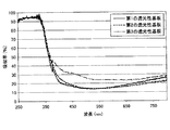
図3には、光散乱層120を有する透明基板110上に被覆層130を形成した後、第1の電極層130層を形成して得られたサンプルにおける、波長250nm〜700nmの範囲の吸収率の測定結果を示す。
FIG. 3 shows an absorptance in a wavelength range of 250 nm to 700 nm in a sample obtained by forming the
なお、第1の電極層130層は、ITOとし、スパッタリング法により成膜した。ITO成膜時の酸素流量は、2.0sccm(第7の透光性基板)、3.0sccm(第6の透光性基板)、4.0sccm(第5の透光性基板)、および5.0sccm(第4の透光性基板)と変化させた。
Note that the
この結果から、ITO成膜時の雰囲気への酸素流量を増加させることにより、すなわちITO成膜時の雰囲気を酸素リッチとすることにより、得られるサンプルの吸収が低下することがわかる。例えば、波長550nmでは、ITO成膜時の酸素流量を2.0sccmとした場合、吸収率は、約15%であるものの、ITO成膜時の酸素流量を5.0sccmとした場合、吸収率は、約9%まで低下した。 From this result, it can be seen that by increasing the oxygen flow rate to the atmosphere during ITO film formation, that is, by making the atmosphere during ITO film formation rich in oxygen, the absorption of the obtained sample is reduced. For example, at a wavelength of 550 nm, the absorption rate is about 15% when the oxygen flow rate during ITO film formation is 2.0 sccm, but when the oxygen flow rate during ITO film formation is 5.0 sccm, the absorption rate is Decreased to about 9%.
この結果から、第1の電極層140が形成された後の段階で、第1の電極層140との界面側における酸化度合いと、被覆層130の内部側の酸化度合いとの差が少なくなるように被覆層130を形成することにより、着色の発生が有意に抑制された有機LED素子100を提供することができることがわかる。
From this result, at the stage after the
次に、本発明による有機LED素子100を構成する各層の詳細について説明する。
Next, the detail of each layer which comprises the
(透明基板110)
透明基板110は、可視光に対する透過率が高い材料で構成される。透明基板110は、例えば、ガラス基板またはプラスチック基板であっても良い。
(Transparent substrate 110)
The
ガラス基板の材料としては、アルカリガラス、無アルカリガラスまたは石英ガラスなどの無機ガラスが挙げられる。また、プラスチック基板の材料としては、ポリエステル、ポリカーボネート、ポリエーテル、ポリスルホン、ポリエーテルスルホン、ポリビニルアルコールならびにポリフッ化ビニリデンおよびポリフッ化ビニルなどのフッ素含有ポリマーが挙げられる。 Examples of the material of the glass substrate include inorganic glass such as alkali glass, non-alkali glass, and quartz glass. Examples of the plastic substrate material include polyester, polycarbonate, polyether, polysulfone, polyethersulfone, polyvinyl alcohol, and fluorine-containing polymers such as polyvinylidene fluoride and polyvinyl fluoride.
透明基板110の厚さは、特に限られないが、例えば、0.1mm〜2.0mmの範囲であっても良い。強度および重量を考慮すると、透明基板110の厚さは、0.5mm〜1.4mmであることが好ましい。
The thickness of the
(光散乱層120)
光散乱層120は、ベース材121と、該ベース材121中に分散された複数の散乱物質124とを有する。ベース材121は、第1の屈折率を有し、散乱物質124は、ベース材とは異なる第2の屈折率を有する。
(Light scattering layer 120)
The
光散乱層120中の散乱物質124の存在量は、光散乱層120の内部から外側に向かって小さくなっていることが好ましく、この場合、高効率の光取り出しを実現することができる。
The amount of the
ベース材121は、ガラスで構成され、ガラスの材料としては、ソーダライムガラス、ホウケイ酸塩ガラス、無アルカリガラス、および石英ガラスなどの無機ガラスが使用される。
The
散乱物質124は、例えば、気泡、析出結晶、ベース材とは異なる材料粒子、分相ガラス等で構成される。分相ガラスとは、2種類以上のガラス相により構成されるガラスをいう。
The
ベース材121の屈折率と散乱物質124の屈折率の差は、大きい方が良く、このためには、ベース材121として高屈折率ガラスを使用し、散乱物質124として気泡を使用することが好ましい。
The difference between the refractive index of the
ベース材121用の高屈折率のガラスのため、ネットワークフォーマとして、P2O5、SiO2、B2O3、GeO2、およびTeO2のうちの一種類または二種類以上の成分を選定し、高屈折率成分として、TiO2、Nb2O5、WO3、Bi2O3、La2O3、Gd2O3、Y2O3、ZrO2、ZnO、BaO、PbO、およびSb2O3のうちの一種類または二種類以上の成分を選定しても良い。さらに、ガラスの特性を調整するため、アルカリ酸化物、アルカリ土類酸化物、フッ化物などを、屈折率に影響を及ぼさない範囲で、添加しても良い。
Because of the high refractive index glass for the
従って、ベース材121を構成するガラス系としては、例えば、B2O3−ZnO−La2O3系、P2O5−B2O3−R'2O−R"O−TiO2−Nb2O5−WO3−Bi2O3系、TeO2−ZnO系、B2O3−Bi2O3系、SiO2−Bi2O3系、SiO2−ZnO系、B2O3−ZnO系、P2O5−ZnO系などが挙げられる。ここで、R'はアルカリ金属元素、R"はアルカリ土類金属元素を示す。なお、以上の材料系は、一例に過ぎず、上記条件を満たすような構成であれば、使用材料は、特に限られない。
Accordingly, examples of the glass system constituting the
ベース材121に、着色剤を添加することにより、発光の色味を変化させることもできる。着色剤としては、遷移金属酸化物、希土類金属酸化物、および金属コロイドなどを、単独でまたは組み合わせて使うことができる。
The color of light emission can be changed by adding a colorant to the
(被覆層130)
被覆層130は、少なくとも一部が金属酸化物または金属酸窒化物で形成される。
(Coating layer 130)
The
金属酸化物または金属酸窒化物を構成する金属種は、特に限られないが、金属種は、例えば、チタン、インジウム、スズ、タングステン、タンタル、および/またはニオブ等を含んでも良い。 The metal species constituting the metal oxide or metal oxynitride is not particularly limited, but the metal species may include, for example, titanium, indium, tin, tungsten, tantalum, and / or niobium.
また、被覆層130は、酸化珪素(SiO2)をさらに含んでも良い。
The
例えば、被覆層130は、酸化チタンと酸化珪素の混合物で構成された層であっても良い。この場合、酸化チタンと酸化珪素の割合は、特に限られないが、両者の比(酸化チタン:酸化珪素)は、重量比で、例えば、80:20〜20:80の範囲であっても良い。特に、酸化チタン:酸化珪素の比は、重量比で、75:25〜40:60の範囲であることが好ましい。
For example, the
また、取り出し効率をより向上させるため、被覆層130の屈折率は、電極140よりも低いことが好ましい。具体的には、被覆層130の屈折率と光散乱層120の屈折率の差は、0.2以下が好ましく、0.13以下がより好ましく、0.11以下がより好ましい。
In order to further improve the extraction efficiency, the refractive index of the
被覆層130の膜厚は、特に限られない。被覆層130の膜厚は、例えば、100nm〜500μmの範囲であっても良い。
The film thickness of the
被覆層130は、湿式コーティング法または乾式コーティング法のいずれで形成されても良い。
The
ここで、本発明では、被覆層130は、第1の電極層140との界面における酸化度合いと内部の酸化度合いとの差が少なくなっていることに留意する必要がある。すなわち、本発明では、被覆層130の最表面に、前述のような変質層80が生じ難くなっており、これにより、着色の問題を有意に抑制することができる。
Here, it should be noted that in the present invention, the
なお、有機LED素子100としての特性(光取り出し効率)考慮した場合、被覆層130は、第1の電極層140との界面側の屈折率と、内部側の屈折率とが接近していることが好ましい。
In addition, when the characteristic (light extraction efficiency) as the
(第1の電極層140)
第1の電極層140には、有機発光層150で生じた光を外部に取り出すため、80%以上の透光性が要求される。また、多くの正孔を注入するため、仕事関数が高いことが要求される。
(First electrode layer 140)
The
第1の電極層140には、例えば、ITO、SnO2、ZnO、IZO(Indium Zinc Oxide)、AZO(ZnO−Al2O3:アルミニウムがドーピングされた亜鉛酸化物)、GZO(ZnO−Ga2O3:ガリウムがドーピングされた亜鉛酸化物)、NbドープTiO2、およびTaドープTiO2などの材料が用いられる。
The
第1の電極層140の厚さは、100nm以上であることが好ましい。
The thickness of the
第1の電極層140の屈折率は、1.75〜2.2の範囲である。例えば、第1の電極層140としてITOを使用した場合、キャリア濃度を増加させることにより、第1の電極層140の屈折率を低下させることができる。市販のITOでは、SnO2が10wt%含まれるものが標準となっているが、Sn濃度をさらに増加させることにより、ITOの屈折率を下げることができる。ただし、Sn濃度の増加により、キャリア濃度は増加するが、移動度および透過率は、低下する。従って、全体のバランスを考慮して、Sn量を決める必要がある。
The refractive index of the
また、第1の電極層140の屈折率は、光散乱層120を構成するベース材121の屈折率や第2の電極層160の屈折率を考慮して、決定することが好ましい。導波路計算や第2の電極層160の反射率等を考慮すると、第1の電極層140とベース材121の屈折率の差は、0.2以下であることが好ましい。
The refractive index of the
ここで、参考のため、光散乱層120〜第1の電極層140の間の各部材の屈折率について示しておく。ただし、以下の屈折率の組み合わせは、単なる一例に過ぎず、各部材は、その他の屈折率を有しても良い。
Here, for reference, the refractive index of each member between the
光散乱層120の屈折率は、例えば1.8〜2.0の範囲(例えば1.84程度)である。また、被覆層130の屈折率は、例えば1.7〜2.0の範囲(例えば1.75程度)である。さらに、第1の電極層140の屈折率は、例えば1.8〜2.2の範囲(例えば1.8程度)である。
The refractive index of the
(有機発光層150)
有機発光層150は、発光機能を有する層であり、通常の場合、ホール注入層と、ホール輸送層と、発光層と、電子輸送層と、電子注入層とにより構成される。ただし、有機発光層150は、発光層を有していれば、必ずしも他の層の全てを有する必要はないことは、当業者には明らかである。なお、通常の場合、有機発光層150の屈折率は、1.7〜1.8の範囲である。
(Organic light emitting layer 150)
The organic
ホール注入層は、第1の電極層140からのホール注入の障壁を低くするため、イオン化ポテンシャルの差が小さいものが好ましい。電極からホール注入層への電荷の注入効率が高まると、有機LED素子100の駆動電圧が下がり、電荷の注入効率が高まる。
The hole injection layer preferably has a small difference in ionization potential in order to lower the hole injection barrier from the
ホール注入層の材料としては、高分子材料または低分子材料が使用される。高分子材料の中では、ポリスチレンスルフォン酸(PSS)がドープされたポリエチレンジオキシチオフェン(PEDOT:PSS)が良く使用され、低分子材料の中では、フタロシアニン系の銅フタロシアニン(CuPc)が広く用いられる。
ホール輸送層は、前述のホール注入層から注入されたホールを発光層に輸送する役割をする。ホール輸送層には、例えば、トリフェニルアミン誘導体、N,N'−ビス(1−ナフチル)−N,N'−ジフェニル−1,1'−ビフェニル−4,4'−ジアミン(NPD)、N,N'−ジフェニル−N,N'−ビス[N−フェニル−N−(2−ナフチル)−4'−アミノビフェニル−4−イル] −1,1'−ビフェニル−4,4'−ジアミン(NPTE)、1,1'−ビス[(ジ−4−トリルアミノ)フェニル]シクロヘキサン(HTM2)、およびN,N'−ジフェニル−N,N'−ビス(3−メチルフェニル)−1,1'−ジフェニル−4,4'−ジアミン(TPD)などが用いられる。
As the material of the hole injection layer, a high molecular material or a low molecular material is used. Among the polymer materials, polyethylene dioxythiophene (PEDOT: PSS) doped with polystyrene sulfonic acid (PSS) is often used, and among the low molecular materials, phthalocyanine-based copper phthalocyanine (CuPc) is widely used. .
The hole transport layer serves to transport holes injected from the hole injection layer to the light emitting layer. Examples of the hole transport layer include a triphenylamine derivative, N, N′-bis (1-naphthyl) -N, N′-diphenyl-1,1′-biphenyl-4,4′-diamine (NPD), N , N′-diphenyl-N, N′-bis [N-phenyl-N- (2-naphthyl) -4′-aminobiphenyl-4-yl] -1,1′-biphenyl-4,4′-diamine ( NPTE), 1,1′-bis [(di-4-tolylamino) phenyl] cyclohexane (HTM2), and N, N′-diphenyl-N, N′-bis (3-methylphenyl) -1,1′- Diphenyl-4,4′-diamine (TPD) or the like is used.
ホール輸送層の厚さは、例えば10nm〜150nmの範囲である。ホール輸送層の厚さが薄いほど、有機LED素子を低電圧化できるが、電極間短絡の問題から、通常は、10nm〜150nmの範囲である。
発光層は、注入された電子とホールが再結合する場を提供する役割を有する。有機発光材料としては、低分子系または高分子系のものが使用される。
The thickness of the hole transport layer is, for example, in the range of 10 nm to 150 nm. The voltage of the organic LED element can be lowered as the thickness of the hole transport layer is reduced, but it is usually in the range of 10 nm to 150 nm due to the problem of short circuit between electrodes.
The light emitting layer has a role of providing a field where the injected electrons and holes are recombined. As the organic light emitting material, a low molecular weight or high molecular weight material is used.
発光層には、例えば、トリス(8−キノリノラート)アルミニウム錯体(Alq3)、ビス(8−ヒドロキシ)キナルジンアルミニウムフェノキサイド(Alq'2OPh)、ビス(8−ヒドロキシ)キナルジンアルミニウム−2,5−ジメチルフェノキサイド(BAlq)、モノ(2,2,6,6−テトラメチル−3,5−ヘプタンジオナート)リチウム錯体(Liq)、モノ(8−キノリノラート)ナトリウム錯体(Naq)、モノ(2,2,6,6−テトラメチル−3,5−ヘプタンジオナート)リチウム錯体、モノ(2,2,6,6−テトラメチル−3,5−ヘプタンジオナート)ナトリウム錯体およびビス(8−キノリノラート)カルシウム錯体(Caq2)などのキノリン誘導体の金属錯体、テトラフェニルブタジエン、フェニルキナクドリン(QD)、アントラセン、ペリレン、並びにコロネンなどの蛍光性物質が挙げられる。 Examples of the light emitting layer include tris (8-quinolinolato) aluminum complex (Alq3), bis (8-hydroxy) quinaldine aluminum phenoxide (Alq′2OPh), and bis (8-hydroxy) quinaldine aluminum-2,5- Dimethylphenoxide (BAlq), mono (2,2,6,6-tetramethyl-3,5-heptanedionate) lithium complex (Liq), mono (8-quinolinolato) sodium complex (Naq), mono (2, 2,6,6-tetramethyl-3,5-heptanedionate) lithium complex, mono (2,2,6,6-tetramethyl-3,5-heptanedionate) sodium complex and bis (8-quinolinolate) Metal complexes of quinoline derivatives such as calcium complex (Caq2), tetraphenyl butadiene, phenyl key Kudrin (QD), anthracene, perylene, as well as fluorescent substance such as coronene.
ホスト材料としては、キノリノラート錯体を使用しても良く、特に、8−キノリノールおよびその誘導体を配位子としたアルミニウム錯体が使用されても良い。
電子輸送層は、電極から注入された電子を輸送する役割をする。電子輸送層には、例えば、キノリノールアルミニウム錯体(Alq3)、オキサジアゾール誘導体(例えば、2,5−ビス(1−ナフチル)−1,3,4−オキサジアゾール(END)、および2−(4−t−ブチルフェニル) −5−(4−ビフェニル))−1,3,4−オキサジアゾール(PBD)など)、トリアゾール誘導体、バソフェナントロリン誘導体、およびシロール誘導体などが用いられる。
電子注入層は、例えば、第2の電極層160との界面に、リチウム(Li)、セシウム(Cs)等のアルカリ金属をドープした層を設けることにより構成される。
As the host material, a quinolinolate complex may be used, and in particular, an aluminum complex having 8-quinolinol and a derivative thereof as a ligand may be used.
The electron transport layer serves to transport electrons injected from the electrode. Examples of the electron transport layer include quinolinol aluminum complex (Alq3), oxadiazole derivatives (for example, 2,5-bis (1-naphthyl) -1,3,4-oxadiazole (END), and 2- ( 4-t-butylphenyl) -5- (4-biphenyl))-1,3,4-oxadiazole (PBD), triazole derivatives, bathophenanthroline derivatives, silole derivatives, and the like.
The electron injection layer is configured by, for example, providing a layer doped with an alkali metal such as lithium (Li) or cesium (Cs) at the interface with the
(第2の電極層160)
第2の電極層160には、仕事関数の小さな金属またはその合金が用いられる。第2の電極層160は、例えば、アルカリ金属、アルカリ土類金属、および周期表第3属の金属などであっても良い。第2の電極層160には、例えば、アルミニウム(Al)、マグネシウム(Mg)、またはこれらの合金などが用いられる。
(Second electrode layer 160)
For the
また、アルミニウム(Al)、マグネシウム銀(MgAg)の共蒸着膜、フッ化リチウム(LiF)または酸化リチウム(Li2O)の薄膜上に、アルミニウム(Al)を蒸着した積層電極が用いられても良い。さらに、カルシウム(Ca)またはバリウム(Ba)と、アルミニウム(Al)との積層膜が用いられても良い。 Also, a laminated electrode in which aluminum (Al) is deposited on a thin film of aluminum (Al), magnesium silver (MgAg), lithium fluoride (LiF), or lithium oxide (Li 2 O) may be used. good. Furthermore, a laminated film of calcium (Ca) or barium (Ba) and aluminum (Al) may be used.
(本発明による有機LED素子の製造方法)
次に、図4を参照して、本発明による有機LED素子の製造方法の一例について説明する。図4には、本発明による有機LED素子を製造する際の概略的なフロー図を示す。
(Method for producing organic LED element according to the present invention)
Next, with reference to FIG. 4, an example of the manufacturing method of the organic LED element by this invention is demonstrated. FIG. 4 shows a schematic flow chart when manufacturing the organic LED element according to the present invention.
図4に示すように、本発明による有機LED素子の製造方法は、
(a)透明基板上に光散乱層を形成するステップ(ステップS110)と、
(b)前記光散乱層上に、被覆層を設置するステップ(ステップS120)と、
(c)前記被覆層上に、第1の電極層を設置するステップ(ステップS130)と、
(d)前記第1の電極層上に、有機発光層を設置するステップ(ステップS140)と、
(e)前記有機発光層上に、第2の電極層を設置するステップ(ステップS150)と、
を有する。以下、各ステップについて詳しく説明する。なお、以下の説明では、明確化のため、各部材の参照符号として、図1に示した参照符号を使用することにする。
As shown in FIG. 4, the manufacturing method of the organic LED element according to the present invention includes:
(A) forming a light scattering layer on the transparent substrate (step S110);
(B) installing a coating layer on the light scattering layer (step S120);
(C) installing a first electrode layer on the coating layer (step S130);
(D) installing an organic light emitting layer on the first electrode layer (step S140);
(E) installing a second electrode layer on the organic light emitting layer (step S150);
Have Hereinafter, each step will be described in detail. In the following description, the reference numerals shown in FIG. 1 are used as reference numerals for each member for the sake of clarity.
(ステップS110)
まず、透明基板が準備される。前述のように、通常、透明基板には、ガラス基板やプラスチック基板が用いられる。
(Step S110)
First, a transparent substrate is prepared. As described above, a glass substrate or a plastic substrate is usually used as the transparent substrate.
次に、透明基板上に、ガラス製のベース材中に散乱物質が分散された光散乱層が形成される。光散乱層の形成方法は、特に限られないが、ここでは、特に、「フリットペースト法」により、光散乱層を形成する方法について説明する。ただし、その他の方法で光散乱層を形成しても良いことは、当業者には明らかである。 Next, a light scattering layer in which a scattering substance is dispersed in a glass base material is formed on the transparent substrate. The method for forming the light scattering layer is not particularly limited, but here, a method for forming the light scattering layer by the “frit paste method” will be particularly described. However, it will be apparent to those skilled in the art that the light scattering layer may be formed by other methods.
フリットペースト法とは、フリットペーストと呼ばれるガラス材料を含むペーストを調製し(調製工程)、このフリットペーストを被設置基板の表面に塗布して、パターン化し(パターン形成工程)、さらにフリットペーストを焼成すること(焼成工程)により、被設置基板の表面に、所望のガラス製の膜を形成する方法である。以下、各工程について簡単に説明する。 In the frit paste method, a paste containing a glass material called a frit paste is prepared (preparation process), this frit paste is applied to the surface of the substrate to be installed, patterned (pattern formation process), and the frit paste is then baked. This is a method of forming a desired glass film on the surface of the substrate to be installed by performing (firing process). Hereinafter, each process will be briefly described.
(調製工程)
まず、ガラス粉末、樹脂、および溶剤等を含むフリットペーストが調製される。
(Preparation process)
First, a frit paste containing glass powder, resin, solvent and the like is prepared.
ガラス粉末は、最終的に光散乱層のベース材を形成する材料で構成される。ガラス粉末の組成は、所望の散乱特性が得られ、フリットペースト化して焼成することが可能なものであれば特に限られない。ガラス粉末の組成は、例えば、P2O5を20〜30mol%、B2O3を3〜14mol%、Bi2O3を10〜20mol%、TiO2を3〜15mol%、Nb2O5を10〜20mol%、WO3を5〜15mol%含み、Li2OとNa2OとK2Oの総量が10〜20mol%であり、以上の成分の総量が、90mol%以上のものであっても良い。また、SiO2は0〜30mol%、B2O3は10〜60mol%、ZnOは0〜40mol%、Bi2O3は0〜40mol%、P2O5は0〜40mol%、アルカリ金属酸化物は0〜20mol%であり、以上の成分の総量が、90mol%以上のものであっても良い。ガラス粉末の粒径は、例えば、1μm〜100μmの範囲である。
A glass powder is comprised with the material which finally forms the base material of a light-scattering layer. The composition of the glass powder is not particularly limited as long as desired scattering characteristics can be obtained, and the glass powder can be frit pasted and fired. The composition of the glass powder, for example, 20 to 30 mol% of P 2 O 5, B 2 O 3 to 3~14mol%, 10~20mol% of Bi 2 O 3, a TiO 2 3~15mol%, Nb 2 O 5 10 to 20 mol%, WO 3 to 5 to 15 mol%, the total amount of Li 2 O, Na 2 O and K 2 O is 10 to 20 mol%, and the total amount of the above components is 90 mol% or more. May be. Further, SiO 2 is 0~30mol%,
なお、最終的に得られる光散乱層の熱膨張特性を制御するため、ガラス粉末には、所定量のフィラーを添加しても良い。フィラーには、例えば、ジルコン、シリカ、またはアルミナなどの粒子が使用され、粒径は、通常、0.1μm〜20μmの範囲である。 In order to control the thermal expansion characteristics of the finally obtained light scattering layer, a predetermined amount of filler may be added to the glass powder. For example, particles such as zircon, silica, or alumina are used as the filler, and the particle size is usually in the range of 0.1 μm to 20 μm.
樹脂には、例えば、エチルセルロース、ニトロセルロース、アクリル樹脂、酢酸ビニル、ブチラール樹脂、メラミン樹脂、アルキッド樹脂、およびロジン樹脂などが用いられる。なお、ブチラール樹脂、メラミン樹脂、アルキッド樹脂、およびロジン樹脂を添加すると、フリットペースト塗布膜の強度が向上する。 Examples of the resin include ethyl cellulose, nitrocellulose, acrylic resin, vinyl acetate, butyral resin, melamine resin, alkyd resin, and rosin resin. Note that the addition of butyral resin, melamine resin, alkyd resin, and rosin resin improves the strength of the frit paste coating film.
溶剤は、樹脂を溶解し、粘度を調整する役割を有する。溶剤には、例えば、エーテル系溶剤(ブチルカルビトール(BC)、ブチルカルビトールアセテート(BCA)、ジプロピレングリコールブチルエーテル、トリプロピレングリコールブチルエーテル、酢酸ブチルセロソルブ)、アルコール系溶剤(α−テルピネオール、パインオイル)、エステル系溶剤(2,2,4−トリメチル−1,3−ペンタンジオールモノイソブチレート)、フタル酸エステル系溶剤(DBP(ジブチルフタレート)、DMP(ジメチルフタレート)、DOP(ジオクチルフタレート))がある。主に用いられているのは、α−テルピネオールや2,2,4−トリメチル−1,3−ペンタンジオールモノイソブチレート)である。なお、DBP(ジブチルフタレート)、DMP(ジメチルフタレート)、DOP(ジオクチルフタレート)は、可塑剤としても機能する。 A solvent has a role which melt | dissolves resin and adjusts a viscosity. Examples of the solvent include ether solvents (butyl carbitol (BC), butyl carbitol acetate (BCA), dipropylene glycol butyl ether, tripropylene glycol butyl ether, butyl cellosolve), alcohol solvents (α-terpineol, pine oil). , Ester solvents (2,2,4-trimethyl-1,3-pentanediol monoisobutyrate), phthalate esters solvents (DBP (dibutyl phthalate), DMP (dimethyl phthalate), DOP (dioctyl phthalate)) is there. Mainly used are α-terpineol and 2,2,4-trimethyl-1,3-pentanediol monoisobutyrate). DBP (dibutyl phthalate), DMP (dimethyl phthalate), and DOP (dioctyl phthalate) also function as a plasticizer.
その他、フリットペーストには、粘度の調整やフリット分散促進のため、界面活性剤を添加しても良い。また、表面改質のため、シランカップリング剤を使用しても良い。 In addition, a surfactant may be added to the frit paste to adjust viscosity and promote frit dispersion. Moreover, you may use a silane coupling agent for surface modification.
次に、これらの原料を混合し、ガラス原料が均一に分散されたフリットペーストを調製する。 Next, these raw materials are mixed to prepare a frit paste in which glass raw materials are uniformly dispersed.
(パターン形成工程)
次に、前述の方法で調製したフリットペーストを、透明基板上に塗布し、パターン化する。塗布の方法およびパターン化の方法は、特に限られない。例えば、スクリーン印刷機を用いて、透明基板上にフリットペーストをパターン印刷しても良い。あるいは、ドクターブレード印刷法またはダイコート印刷法を利用しても良い。
(Pattern formation process)
Next, the frit paste prepared by the above-described method is applied on a transparent substrate and patterned. The application method and the patterning method are not particularly limited. For example, a frit paste may be pattern-printed on a transparent substrate using a screen printer. Alternatively, a doctor blade printing method or a die coat printing method may be used.
その後、フリットペースト膜は、乾燥される。 Thereafter, the frit paste film is dried.
(焼成工程)
次に、フリットペースト膜が焼成される。通常、焼成は、2段階のステップで行われる。第1のステップでは、フリットペースト膜中の樹脂が分解、消失され、第2のステップでは、ガラス粉末が軟化、焼結される。
(Baking process)
Next, the frit paste film is baked. Usually, firing is performed in two steps. In the first step, the resin in the frit paste film is decomposed and disappeared, and in the second step, the glass powder is softened and sintered.
第1のステップは、大気雰囲気下で、フリットペースト膜を200℃〜400℃の温度範囲に保持することにより行われる。ただし、処理温度は、フリットペーストに含まれる樹脂の材料によって変化する。例えば、樹脂がエチルセルロースの場合は、処理温度は、350℃〜400℃程度であり、樹脂がニトロセルロースの場合は、処理温度は、200℃〜300℃程度であっても良い。なお処理時間は、通常、30分から1時間程度である。 The first step is performed by maintaining the frit paste film in a temperature range of 200 ° C. to 400 ° C. in an air atmosphere. However, the processing temperature varies depending on the resin material contained in the frit paste. For example, when the resin is ethyl cellulose, the treatment temperature may be about 350 ° C. to 400 ° C., and when the resin is nitrocellulose, the treatment temperature may be about 200 ° C. to 300 ° C. The processing time is usually about 30 minutes to 1 hour.
第2のステップは、大気雰囲気下で、フリットペースト膜を、含まれるガラス粉末の軟化温度±30℃の温度範囲に保持することにより行われる。処理温度は、例えば、450℃〜600℃の範囲である。また、処理時間は、特に限られないが、例えば、30分〜1時間である。 The second step is performed by maintaining the frit paste film in the temperature range of the softening temperature ± 30 ° C. of the glass powder contained in the atmosphere. The processing temperature is, for example, in the range of 450 ° C to 600 ° C. Further, the processing time is not particularly limited, but is, for example, 30 minutes to 1 hour.
第2のステップ後に、ガラス粉末が軟化、焼結して、光散乱層のベース材が形成される。また、フリットペースト膜中に内包させた散乱物質によって、例えば内在する気泡などによって、ベース材中に均一に分散された散乱物質が得られる。 After the second step, the glass powder is softened and sintered to form a base material for the light scattering layer. Further, the scattering material uniformly dispersed in the base material can be obtained by the scattering material encapsulated in the frit paste film, for example, due to the bubbles present therein.
その後、透明基板を冷却することにより、側面部分が上面から前記底面に向かって、直角よりも緩やかな角度で傾斜した表面を有する光散乱層が形成される。 Thereafter, by cooling the transparent substrate, a light scattering layer having a surface whose side surface portion is inclined at a gentler angle than a right angle from the upper surface toward the bottom surface is formed.
最終的に得られる光散乱層の厚さは、5μm〜50μmの範囲であっても良い。 The thickness of the finally obtained light scattering layer may be in the range of 5 μm to 50 μm.
(ステップS120)
次に、前記工程で得られた光散乱層上に、被覆層が設置される。一般に、被覆層は、金属酸化物または金属酸窒化物で構成される。
(Step S120)
Next, a coating layer is placed on the light scattering layer obtained in the above step. Generally, a coating layer is comprised with a metal oxide or a metal oxynitride.
被覆層は、例えば、乾式コーティング法により形成される。あるいは、被覆層は、例えば、湿式コーティング法により形成されても良い。湿式コーティング法の種類は、特に限られないが、ここでは、有機金属溶液と有機金属粒子を含むゾルゲル液を用いて、被覆層を形成する方法について説明する。ただし、これ以外の湿式コーティング法で、被覆層を形成しても良い。 The coating layer is formed by, for example, a dry coating method. Alternatively, the coating layer may be formed by, for example, a wet coating method. The type of wet coating method is not particularly limited, but here, a method of forming a coating layer using a sol-gel solution containing an organometallic solution and organometallic particles will be described. However, the coating layer may be formed by other wet coating methods.
有機金属溶液と有機金属粒子を含むゾルゲル液を使用して被覆層を形成する場合、光散乱層上にゾルゲル液を塗布する工程(塗布工程)と、塗布されたゾルゲル層を乾燥する工程(乾燥工程)と、乾燥されたゾルゲル層を熱処理する工程(熱処理工程)とを経て、被覆層が形成される。以下、各工程について簡単に説明する。 When forming a coating layer using a sol-gel solution containing an organometallic solution and organometallic particles, a step of applying the sol-gel solution on the light scattering layer (application step) and a step of drying the applied sol-gel layer (drying) The coating layer is formed through a step) and a step of heat-treating the dried sol-gel layer (heat treatment step). Hereinafter, each process will be briefly described.
(塗布工程)
まず、光散乱層上にゾルゲル液が塗布される。ゾルゲル液は、有機金属溶液と有機金属粒子を含む。
(Coating process)
First, a sol-gel solution is applied on the light scattering layer. The sol-gel solution includes an organometallic solution and organometallic particles.
有機金属溶液は、チタン、ニオブ、ジルコニウム、タンタル、シリコンのアルコキシドや有機錯体である。また、これに加えて、有機金属溶液は、有機シラン等のような酸化珪素源を有しても良い。 The organometallic solution is an alkoxide or organic complex of titanium, niobium, zirconium, tantalum, silicon. In addition, the organometallic solution may have a silicon oxide source such as organosilane.
有機金属粒子は、例えば、有機チタン、有機ニオブ、有機ジルコニウム、および/または有機タンタルのオリゴマーや粒子を含んでも良い。また、ゾルゲル液の溶媒は、特に限られず、溶媒として、水および/または有機溶剤が使用されても良い。 The organometallic particles may include, for example, organotitanium, organoniobium, organozirconium, and / or organotantalum oligomers and particles. The solvent of the sol-gel solution is not particularly limited, and water and / or an organic solvent may be used as the solvent.
有機金属溶液は、以下の具体例に限定はされないが、例えば、チタンテトラメトキシド、チタンテトラエトキシド、チタンテトラノルマルプロポキシド、チタンテトライソプロポキシド、チタンテトラノルマルブトキシド、チタンテトライソブトキシド、チタンジイソプロポキシジノルマルブトキド、チタンジターシャリーブトキシジイソプロポキシド、チタンテトラターシャリーブトキシド、チタンテトラペントキシド、チタンテトラヘキソキシド、チタンテトラヘプトキシド、チタンテトライソオクチルオキシド、テトラステアリルアルコキシチタネートなどのチタンアルコキシド、チタンテトラシクロヘキソキシドなどのチタンテトラシクロアルキルオキシド、チタンテトラフェノキシドなどのチタンアリールオキシド、ヒドロキシチタンステアレートなどのチタンアシレート、ジプロポキシチタンビス(アセチルアセトネート)、チタンテトラアセチルアセトネート、チタンジ-2-エチルヘキソキシビス(2-エチル-3-ヒドロキシヘキソキシド)、チタンジイソプロポキシビス(エチルアセトアセテート)、チタンジイソプロポキシビス(トリエタノールアミネート)、チタンラクテートアンモニウム塩、チタンラクテートなどのチタンキレート、ジルコニウムテトラノルマルプロポキシド、ジルコニウムテトラノルマルブトキシドなどのアルコキシジルコニウム、ジルコニウムトリブトキシモノステアレート、塩化ジルコニウム化合物やアミノカルボン酸ジルコニウムなどのジルコニウムアシレート、ジルコニウムテトラアセチルアセトネート、ジルコニウムトリブトキシモノアセチルアセトネート、ジルコニウムジブトキシビス(エチルアセトアセテート)、ジルコニウムテトラアセチルアセトネートなどのジルコニウムキレート、テトラメトキシシラン、メチルトリメトキシシラン、ジメチルジメトキシシラン、フェニルトリメトキシシラン、ジフェニルジメトキシシラン、ヘキシルトリメトキシシラン、デシルトリメトキシシラン、ビニルトリメトキシシラン、2-(3,4-エポキシシクロヘキシル)エチルトリメトキシシラン、3-グリシドキシプロピルメチルジメトキシシラン、3−(グリシジロキシ)プロピルトリメトキシシラン、トリフルオロプロピルトリメトキシシラン、p-スチリルトリメトキシシラン、3-メタクリロキシプロピルメチルジメトキシシラン、3-メタクリロキシプロピルトリメトキシシラン、3-アクリロキシプロピルトリメトキシシラン、N-2-(アミノエチル)-3-アミノプロピルメチルジメトキシシラン、N-3-(アミノエチル)-3-アミノプロピルトリメトキシシラン、N-フェニル-3-アミノプロピルトリメトキシシラン、3-メルカプトプロピルメチルジメトキシシラン、3-メルカプトプロピルトリメトキシシラン、テトラエトキシシラン、メチルトリエトキシシラン、ジメチルジエトキシシラン、フェニルトリエトキシシラン、ジフェニルジエトキシシラン、3-メタクリロキシプロピルメチルジエトキシシラン、3-メタクリロキシプロピルトリエトキシシラン、ヘキシルトリエトキシシラン、ビニルトリエトキシシラン、3-グリシドキシプロピルメチルジエトキシシラン、3-グリシドキシプロピルトリエトキシシラン、N-2-(アミノエチル)-3-アミノプロピルトリエトキシシラン、3-アミノプロピルトリメトキシシラン、3-トリエトキシシリル-N-(1,3-ジメチル-ブチリデン)プロピルアミン、3-ウレイドプロピルトリエトキシシラン、3-イソシアネートプロピルトリエトキシシラン、テトラノルマルプロポキシシラン、テトライソプロポキシシラン、テトラノルマルブトキシシラン、テトライソブトキシシラン、ジイソプロポキシジノルマルブトキシシラン、ジターシャリーブトキシジイソプロポキシシラン、テトラターシャリーブトキシシラン、テトラペントキシシラン、テトラヘキソキシシラン、テトラヘプトキシシラン、テトライソオクチルオキシシラン、テトラステアリルアルコキシシランなどのアルコキシシラン類、ヘキサメチルジシラザン等のシラザン類とアルコール、エーテル、ケトン、炭化水素類の溶剤で構成されるものが例示される。 The organic metal solution is not limited to the following specific examples. For example, titanium tetramethoxide, titanium tetraethoxide, titanium tetranormal propoxide, titanium tetraisopropoxide, titanium tetranormal butoxide, titanium tetraisobutoxide, titanium Diisopropoxy dinormal butoxide, titanium ditertiary butoxy diisopropoxide, titanium tetratertiary butoxide, titanium tetrapentoxide, titanium tetrahexoxide, titanium tetraheptoxide, titanium tetraisooctyl oxide, tetrastearyl alkoxy titanate Titanium alkoxide, titanium tetracyclooxide such as titanium tetracyclohexoxide, titanium aryloxide such as titanium tetraphenoxide, hydroxy Titanium acylates such as Nstearate, dipropoxy titanium bis (acetylacetonate), titanium tetraacetylacetonate, titanium di-2-ethylhexoxybis (2-ethyl-3-hydroxyhexoxide), titanium diisopropoxybis (Ethyl acetoacetate), titanium diisopropoxybis (triethanolaminate), titanium lactate ammonium salt, titanium chelate such as titanium lactate, alkoxy zirconium such as zirconium tetranormal propoxide, zirconium tetranormal butoxide, zirconium tributoxy monostearate Rate, zirconium acylates such as zirconium chloride and zirconium aminocarboxylate, zirconium tetraacetylacetonate, zirconium tributoxy Zirconium chelates such as monoacetylacetonate, zirconium dibutoxybis (ethylacetoacetate), zirconium tetraacetylacetonate, tetramethoxysilane, methyltrimethoxysilane, dimethyldimethoxysilane, phenyltrimethoxysilane, diphenyldimethoxysilane, hexyltrimethoxy Silane, decyltrimethoxysilane, vinyltrimethoxysilane, 2- (3,4-epoxycyclohexyl) ethyltrimethoxysilane, 3-glycidoxypropylmethyldimethoxysilane, 3- (glycidyloxy) propyltrimethoxysilane, trifluoropropyl Trimethoxysilane, p-styryltrimethoxysilane, 3-methacryloxypropylmethyldimethoxysilane, 3-methacryloxypropyltrimethoxy Lan, 3-acryloxypropyltrimethoxysilane, N-2- (aminoethyl) -3-aminopropylmethyldimethoxysilane, N-3- (aminoethyl) -3-aminopropyltrimethoxysilane, N-phenyl-3 -Aminopropyltrimethoxysilane, 3-mercaptopropylmethyldimethoxysilane, 3-mercaptopropyltrimethoxysilane, tetraethoxysilane, methyltriethoxysilane, dimethyldiethoxysilane, phenyltriethoxysilane, diphenyldiethoxysilane, 3-methacrylic Roxypropylmethyldiethoxysilane, 3-methacryloxypropyltriethoxysilane, hexyltriethoxysilane, vinyltriethoxysilane, 3-glycidoxypropylmethyldiethoxysilane, 3-glycidoxypropyltriethoxysilane N-2- (aminoethyl) -3-aminopropyltriethoxysilane, 3-aminopropyltrimethoxysilane, 3-triethoxysilyl-N- (1,3-dimethyl-butylidene) propylamine, 3-ureido Propyltriethoxysilane, 3-isocyanatopropyltriethoxysilane, tetranormalpropoxysilane, tetraisopropoxysilane, tetranormalbutoxysilane, tetraisobutoxysilane, diisopropoxydinormalbutoxysilane, ditertiarybutoxydiisopropoxysilane, tetra Alkoxysilanes such as tertiary butoxysilane, tetrapentoxysilane, tetrahexoxysilane, tetraheptoxysilane, tetraisooctyloxysilane, tetrastearylalkoxysilane, hexamethyldi Examples include those composed of silazanes such as silazane and alcohol, ether, ketone, and hydrocarbon solvents.
これら有機金属である、チタン、ニオブ、ジルコニウム、タンタル、シリコンのアルコキシドやキレート化合物類は、縮合させることによって、チタン、ニオブ、ジルコニウム、タンタル、シリコン化合物オリゴマーを用いることがより好ましい。縮合させる方法は特に限定はないが、水をアルコール溶液中で反応させることが好ましい。縮合させることにより、製膜時のクラックを抑制することができ、厚膜を形成することができる。また、特に、有機シラン化合物を混合することにより、製膜時のクラックを抑制することができ、厚膜を形成することができる。また、膜の屈折率を調整することができる。 It is more preferable to use titanium, niobium, zirconium, tantalum, silicon alkoxides and chelate compounds such as these organic metals to condense titanium, niobium, zirconium, tantalum, and silicon compound oligomers. The method of condensation is not particularly limited, but it is preferable to react water in an alcohol solution. By condensing, cracks during film formation can be suppressed, and a thick film can be formed. In particular, by mixing an organosilane compound, cracks during film formation can be suppressed and a thick film can be formed. In addition, the refractive index of the film can be adjusted.
ゾルゲル液を塗布する方法は、特に限られない。ゾルゲル液は、一般的な塗膜形成装置(スピンコーターやアプリケータ等)を使用して、光散乱層上に塗布しても良い。 The method for applying the sol-gel solution is not particularly limited. The sol-gel solution may be applied onto the light scattering layer using a general coating film forming apparatus (spin coater, applicator, etc.).
ゾルゲル液を塗布する方法は、特に限られない。ゾルゲル液は、一般的な塗膜形成装置(アプリケータ等)を使用して、光散乱層上に塗布しても良い。 The method for applying the sol-gel solution is not particularly limited. The sol-gel solution may be applied on the light scattering layer using a general coating film forming apparatus (such as an applicator).
(乾燥工程)
次に、光散乱層上に塗布されたゾルゲル液が乾燥処理され、ゾルゲル層が形成される。乾燥条件は、特に限られない。乾燥は、例えば、ゾルゲル液が塗布された光散乱層付き透明基板を、80℃〜120℃の温度で、1分〜1時間程度保持することにより、実施しても良い。
(Drying process)
Next, the sol-gel liquid applied on the light scattering layer is dried to form a sol-gel layer. Drying conditions are not particularly limited. Drying may be performed, for example, by holding a transparent substrate with a light scattering layer coated with a sol-gel solution at a temperature of 80 ° C. to 120 ° C. for about 1 minute to 1 hour.
(熱処理工程)
次に、乾燥処理されたゾルゲル層が高温に保持される。これにより、ゾルゲル層中の溶媒が完全に蒸発、分解、および/または焼失するとともに、ゾルゲル層中の有機金属化合物が酸化および結合され、被覆層が形成される。
(Heat treatment process)
Next, the dried sol-gel layer is kept at a high temperature. As a result, the solvent in the sol-gel layer is completely evaporated, decomposed, and / or burned out, and the organometallic compound in the sol-gel layer is oxidized and bonded to form a coating layer.
これにより、例えば、チタニアおよびシリカの混合物等で構成された被覆層が形成される。 Thereby, for example, a coating layer composed of a mixture of titania and silica or the like is formed.
熱処理の条件は、特に限られない。例えば、保持温度は、450℃〜550℃の範囲であり、保持時間は、10分〜24時間の範囲であっても良い。 The conditions for the heat treatment are not particularly limited. For example, the holding temperature may be in the range of 450 ° C. to 550 ° C., and the holding time may be in the range of 10 minutes to 24 hours.
以上の工程により、被覆層が形成される。 The coating layer is formed by the above steps.
ここで、前述のように、被覆層130は、第1の電極層140が形成された後の段階において、第1の電極層140との界面側における酸化度合いと、被覆層130の内部側の酸化度合いとの差が少ないという特徴を有する。
Here, as described above, the
被覆層130をこのような特徴を有する構成とすることにより、着色の発生が有意に抑制され、最終的に得られる有機LED素子100において、内部での光の吸収が少なくなり、光取り出し効率を有意に高めることが可能になる。
By making the
なお、このような特徴を有する被覆層130は、大きく分けて、以下の2種類の方法により形成することができる。
(第1の方法)被覆層130の成膜の段階で、予め、最表面側の金属酸化物が「酸素リッチ」な状態となるようにする;および
(第2の方法)第1の電極層140を成膜する際の成膜条件を、「酸素リッチ」な条件とする。
Note that the
(First method) In the stage of forming the
以下、第1および第2の方法について、簡単に説明する。 Hereinafter, the first and second methods will be briefly described.
(第1の方法)
第1の方法では、第1の電極層140の成膜前に、被覆層130の最表面が、予め酸素過剰の状態とされる。
(First method)
In the first method, before the
このような状態の被覆層130は、例えば、被覆層の最表面に、乾式コーティングプロセス等により、酸素リッチな条件下で酸化物膜を成膜することなどにより、容易に得ることができる。乾式コーティングプロセスとしては、スパッタリング法、物理気相成膜法、化学気相成膜法など、各種方法が適用され得る。
The
被覆層130がこのような酸素過剰の状態の最表面を有する場合、以降の第1の電極層140の成膜の段階で、前述のような、被覆層130から第1の電極層140への酸素の移動が生じても、被覆層130の最表面には、未だ十分な酸素が残る。このため、変質層80の発生を有意に抑制することができる。
When the
(第2の方法)
第2の方法では、第1の電極層140を成膜する際の成膜条件を「酸素リッチ」な条件として、第1の電極層140が成膜される。
(Second method)
In the second method, the
従って、この工程の詳細は、ステップS130において説明するが、この方法のように、第1の電極層140を形成する際の成膜条件を、酸素リッチな条件とした場合、被覆層130から第1の電極層140への酸素の移動がより生じにくくなる。従って、この場合も、変質層80の発生を有意に抑制することができる。
Therefore, details of this process will be described in step S130. However, when the film forming conditions for forming the
(ステップS130)
次に、前記工程で得られた被覆層130上に、透明な第1の電極層(陽極)140が設置される。
(Step S130)
Next, a transparent first electrode layer (anode) 140 is placed on the
第1の電極層140の設置方法は、特に限られず、例えば、スパッタ法、蒸着法、および気相成膜法等の成膜法を利用しても良い。
The method for installing the
前述のように、第1の電極層140の材料は、ITO等であっても良い。また、第1の電極層140の厚さは、特に限られず、第1の電極層140の厚さは、例えば50nm〜1.0μmの範囲であっても良い。
As described above, the material of the
また、第1の電極層140は、エッチング処理等により、パターン化しても良い。
Further, the
なお、前述のステップS120において記載したような第2の方法を採用した場合、このステップS130は、「酸素リッチ」な条件下で実施される。 In addition, when the second method as described in step S120 described above is employed, step S130 is performed under “oxygen-rich” conditions.
例えば、ITOのような第1の電極層140を、スパッタリング法で形成する場合、成膜雰囲気を、通常よりも酸素過剰な条件にして、第1の電極層140の成膜処理が行われる。あるいは、ITOのような第1の電極層140を、化学気相成膜法で形成する場合、原料中の金属に対する酸素の割合が高くなるような条件にして、第1の電極層140の成膜処理が行われる。
For example, in the case where the
これにより、第1の電極層140の成膜中に、被覆層130の最表面に変質層が生じ難くなる。従って、被覆層130の着色の問題を有意に抑制することができる。
This makes it difficult for an altered layer to form on the outermost surface of the
ここまでの工程で得られた、透明基板、光散乱層、被覆層、および第1の電極層を有する積層体は、「透光性基板」と呼ばれる。次工程以降に設置される有機発光層、および第2の電極層等の仕様は、最終的に得られる有機LED素子の適用用途によって、様々に変化する。従って、慣用的には、この「透光性基板」は、この状態のまま、中間製品として市場に流通される場合も多く、これ以降の工程が省略される場合も多々ある。 The laminate having the transparent substrate, the light scattering layer, the coating layer, and the first electrode layer obtained through the steps so far is referred to as a “translucent substrate”. The specifications of the organic light-emitting layer, the second electrode layer, and the like installed after the next step vary depending on the application application of the finally obtained organic LED element. Therefore, conventionally, the “translucent substrate” is often distributed in the market as an intermediate product in this state, and the subsequent steps are often omitted.
(ステップS140)
次に、第1の電極層を覆うように、有機発光層が設置される。有機発光層の設置方法は、特に限られず、例えば、蒸着法および/または塗布法を使用しても良い。
(Step S140)
Next, an organic light emitting layer is provided so as to cover the first electrode layer. The installation method of the organic light emitting layer is not particularly limited, and for example, a vapor deposition method and / or a coating method may be used.
(ステップS150)
次に、有機発光層上に第2の電極層が設置される。第2の電極層の設置方法は、特に限られず、例えば、蒸着法、スパッタ法、気相成膜法等を使用しても良い。
(Step S150)
Next, a second electrode layer is disposed on the organic light emitting layer. The installation method of the second electrode layer is not particularly limited, and for example, an evaporation method, a sputtering method, a vapor deposition method, or the like may be used.
以上の工程により、図1に示したような有機LED素子100が製造される。ただし、前述の有機LED素子の製造方法は、一例であって、その他の方法で有機LED素子を製造しても良いことは、当業者には明らかである。
Through the above steps, the
次に、本発明の実施例について説明する。 Next, examples of the present invention will be described.
以下の方法により、各種透過性基板を製作し、それらの特性を評価した。 Various transparent substrates were manufactured by the following method and their characteristics were evaluated.
(各種透過性基板の作製)
透明基板として、縦50mm×横50mm×厚さ0.55mmのソーダライム基板を準備した。また、この透明基板の上に各種層を形成して、合計3種類の透光性基板を作製した。
(Manufacture of various transparent substrates)
A soda-lime substrate having a length of 50 mm, a width of 50 mm, and a thickness of 0.55 mm was prepared as a transparent substrate. Moreover, various layers were formed on this transparent substrate, and a total of three types of translucent substrates were produced.
(第1の透光性基板)
まず、透明基板の上に光散乱層を形成した。
(First translucent substrate)
First, a light scattering layer was formed on a transparent substrate.
光散乱層は、以下の方法により形成した。 The light scattering layer was formed by the following method.
(光散乱層の形成)
以下の方法で、光散乱層用の原料を調製した。
(Formation of light scattering layer)
A raw material for the light scattering layer was prepared by the following method.
まず、表1に示す組成の混合粉末を調合し、溶解した。溶解は、1050℃で1.5時間保持後、950℃で30分間保持することにより実施した。その後、溶解物を双ロールにキャストして、フレーク状ガラスを得た。 First, a mixed powder having the composition shown in Table 1 was prepared and dissolved. The dissolution was carried out by holding at 1050 ° C. for 1.5 hours and then holding at 950 ° C. for 30 minutes. Thereafter, the melt was cast into twin rolls to obtain flaky glass.

次に、このフレーク状ガラスをジルコニア製の遊星ボールミルで2時間乾式粉砕し、平均粒径(d50:積算値50%の粒度、単位μm)が1〜3μmのガラス粉末を調製した。 Next, this flaky glass was dry-pulverized with a zirconia planetary ball mill for 2 hours to prepare glass powder having an average particle size (d 50 : particle size of 50% integrated value, unit μm) of 1 to 3 μm.
次に、このガラス粉末75gに直径3μmのシリカ球を15vol%加え、有機ベヒクル(a−テルピネオール等にエチルセルロースを10質量%程度溶解したもの)25gと混練して、ガラスペーストを作製した。さらに、スクリーン印刷機を用いて、このガラスペーストをソーダライム基板上に印刷した。これにより、ソーダライム基板上に直径10mmφの円状の散乱層を2つ有するパターンを形成した。スクリーン印刷後、ソーダライム基板を120℃で10分間乾燥した。 Next, 15 vol% of silica spheres having a diameter of 3 μm were added to 75 g of this glass powder, and kneaded with 25 g of an organic vehicle (a solution of about 10% by mass of ethyl cellulose in a-terpineol or the like) to prepare a glass paste. Further, this glass paste was printed on a soda lime substrate using a screen printer. As a result, a pattern having two circular scattering layers having a diameter of 10 mmφ was formed on the soda lime substrate. After screen printing, the soda lime substrate was dried at 120 ° C. for 10 minutes.
このソーダライム基板を45分かけて450℃まで昇温した後、450℃で10時間保持した後、12分で575℃まで昇温し、575℃で40分間保持し、その後室温まで3時間で降温した。焼成後の膜厚は15.0μmであった。次に、上述のシリカ球を含まないペーストを上述と同様に作製し、散乱層の上にカバー層を同様に形成した。ここで、カバー層の膜厚は15.0μmであった。これらにより、ソーダライム基板上にカバー層付き光散乱層が形成された。 The soda lime substrate was heated to 450 ° C. over 45 minutes, held at 450 ° C. for 10 hours, then heated to 575 ° C. in 12 minutes, held at 575 ° C. for 40 minutes, and then to room temperature in 3 hours. The temperature dropped. The film thickness after firing was 15.0 μm. Next, the above paste containing no silica sphere was prepared in the same manner as described above, and a cover layer was similarly formed on the scattering layer. Here, the film thickness of the cover layer was 15.0 μm. As a result, a light scattering layer with a cover layer was formed on the soda lime substrate.
光散乱層の厚さは、合計で30μmであった。 The total thickness of the light scattering layer was 30 μm.
(被覆層の形成)
次に、光散乱層の上に被覆層を形成した。
(Formation of coating layer)
Next, a coating layer was formed on the light scattering layer.
被覆層は、以下の方法により、光散乱層上に成膜した。 The coating layer was formed on the light scattering layer by the following method.
まず、チタネートテトラノルマルブトキシドと、3−グリシジロキシプロピルトリメトキシシランを40:60(体積比)の割合で混合したものを、溶剤(1−ブタノール)で希釈し、塗布に適した粘度を持つ被覆層形成用の液体を得た。この被覆層形成用の液体を、ガラス基板上に形成した光散乱層上に滴下し、スピンコーターを用いて塗布膜を形成した。 First, a mixture of titanate tetranormal butoxide and 3-glycidyloxypropyltrimethoxysilane in a ratio of 40:60 (volume ratio) is diluted with a solvent (1-butanol) and has a viscosity suitable for coating. A liquid for forming a coating layer was obtained. The coating layer forming liquid was dropped on the light scattering layer formed on the glass substrate, and a coating film was formed using a spin coater.
塗布膜を120℃に保持した乾燥機に投入、10分間保持することにより、乾燥膜厚0.6μmの乾燥膜を得た。 The coating film was put into a drier maintained at 120 ° C. and held for 10 minutes to obtain a dry film having a dry film thickness of 0.6 μm.
乾燥膜は、475℃で1時間保持して焼成し、これにより150nmの焼成膜を得た。 The dried film was baked by holding at 475 ° C. for 1 hour, thereby obtaining a baked film of 150 nm.
再度、焼成膜の上に被覆層形成用の液体を塗布し、乾燥、焼成し、2層積層することにより、300nmの焼成膜で形成された被覆層(第1部分)を得た。 Again, a coating layer-forming liquid was applied onto the fired film, dried, fired, and laminated to obtain a coating layer (first portion) formed of a 300 nm fired film.
次に、被覆層(第1部分)の上に、反応性スパッタリング法により、SiO2膜を形成した。 Next, a SiO 2 film was formed on the coating layer (first portion) by reactive sputtering.
ターゲットには、SiO2ターゲット(4インチφ、旭硝子社製)を用い、スパッタ電源には、RF電源(JRF−750:日本電子社製)を用いた。チャンバ内の到達真空度は、4×10⁻⁴Paとし、チャンバ内には、Arと酸素の混合ガスを供給した。Arガスの流速は、50sccmであり、酸素ガスの流速は、50sccmとした。全圧は、0.3Paとし、印加電力は、300Wとした。基板加熱温度設定は、500℃とした。 An SiO 2 target (4 inches φ, manufactured by Asahi Glass Co., Ltd.) was used as the target, and an RF power source (JRF-750: manufactured by JEOL Ltd.) was used as the sputtering power source. The ultimate vacuum in the chamber was 4 × 10 −4 Pa, and a mixed gas of Ar and oxygen was supplied into the chamber. The flow rate of Ar gas was 50 sccm, and the flow rate of oxygen gas was 50 sccm. The total pressure was 0.3 Pa and the applied power was 300 W. The substrate heating temperature was set to 500 ° C.
成膜後に得られたSiO2膜の厚さは、約30nmであった。 The thickness of the SiO 2 film obtained after the film formation was about 30 nm.
これにより、TiO2とSiO2からなる第1の部分、およびSiO2からなる第2の部分を有する被覆層が得られた。 Thus, a first part consisting of TiO 2 and SiO 2, and the coating layer having a second portion made of SiO 2 was obtained.
(電極層の形成)
次に、被覆層の上に電極層を形成した。
(Formation of electrode layer)
Next, an electrode layer was formed on the coating layer.
電極層は、反応性スパッタリング法により、被覆層上に成膜した。 The electrode layer was formed on the coating layer by reactive sputtering.
ターゲットには、ITOターゲット(4インチφ、17wt%SnO2−83wt%In2O3、住友金属鉱山社製)を使用した。スパッタ電源には、DC電源(MDX:アドバンスエナジー社製)とパルス化電源(Sparcle−V:アドバンスエナジー社製)とを接続して使用した。 An ITO target (4 inch φ, 17 wt% SnO 2 -83 wt% In 2 O 3 , manufactured by Sumitomo Metal Mining Co., Ltd.) was used as the target. A DC power source (MDX: manufactured by Advanced Energy) and a pulsed power source (Sparkle-V: manufactured by Advanced Energy) were connected to the sputtering power source.
チャンバ内の到達真空度は、4×10⁻⁴Paとし、チャンバ内には、Arと酸素の混合ガスを供給した。Arガスの流速は、50sccmであり、酸素ガスの流速は、1sccmとした。全圧は、0.3Paとし、印加電力は、200Wとした。基板加熱温度設定は、500℃とした。 The ultimate vacuum in the chamber was 4 × 10 −4 Pa, and a mixed gas of Ar and oxygen was supplied into the chamber. The flow rate of Ar gas was 50 sccm, and the flow rate of oxygen gas was 1 sccm. The total pressure was 0.3 Pa and the applied power was 200 W. The substrate heating temperature was set to 500 ° C.
成膜後に得られたITO電極層の厚さは、約150nmであった。 The thickness of the ITO electrode layer obtained after the film formation was about 150 nm.
以上の工程により、第1の透光性基板を作製した。 Through the above steps, a first light-transmitting substrate was manufactured.
なお、目視観察の結果、第1の透光性基板には、着色は認められなかった。 In addition, as a result of visual observation, coloring was not recognized by the 1st translucent board | substrate.
(第2の透光性基板)
前述の第1の透光性基板と同様の方法で、第2の透光性基板を作製した。ただし、この第2の透光性基板の作製の際には、被覆層の第2の部分は、SiSnO膜とした。
(Second translucent substrate)
A second light-transmitting substrate was manufactured in the same manner as the first light-transmitting substrate described above. However, when the second translucent substrate was manufactured, the second portion of the coating layer was a SiSnO film.
このSiSnO膜は、反応性スパッタリング法により、被覆層の第1の部分の上に形成した。 This SiSnO film was formed on the first portion of the coating layer by reactive sputtering.
ターゲットには、SiSnターゲット(35at%Si−65at%Sn、70mm×200mm)を用い、スパッタ電源には、DC電源(MDX:アドバンスエナジー社製)とパルス化電源(Sparcle−V:アドバンスエナジー社製)とを接続して使用した。チャンバ内の到達真空度は、4×10⁻⁴Paとし、チャンバ内には、Arと酸素の混合ガスを供給した。Arガスの流速は、30sccmであり、酸素ガスの流速は、20sccmとした。全圧は、0.3Paとし、印加電力は、500Wとした。基板加熱は行わなかった。 A SiSn target (35 at% Si-65 at% Sn, 70 mm × 200 mm) is used as the target, and a DC power supply (MDX: manufactured by Advanced Energy) and a pulsed power supply (Sparkle-V: manufactured by Advanced Energy) are used as the sputtering power supply. ) And used. The ultimate vacuum in the chamber was 4 × 10 −4 Pa, and a mixed gas of Ar and oxygen was supplied into the chamber. The flow rate of Ar gas was 30 sccm, and the flow rate of oxygen gas was 20 sccm. The total pressure was 0.3 Pa and the applied power was 500 W. No substrate heating was performed.
成膜後に得られたSiSnO膜の厚さは、約100nmであった。 The thickness of the SiSnO film obtained after the film formation was about 100 nm.
これにより、TiO2とSiO2からなる第1の部分、およびSiSnOからなる第2の部分を有する被覆層が得られた。 Thus, a first part consisting of TiO 2 and SiO 2, and the coating layer having a second portion consisting of SiSnO was obtained.
その後、前述の第1の透光性基板と同様の方法で、電極層の成膜を行い、第2の透光性基板を作製した。 After that, an electrode layer was formed by the same method as that for the first light-transmitting substrate described above to produce a second light-transmitting substrate.
なお、目視観察の結果、得られた第2の透光性基板に、着色は認められなかった。 In addition, as a result of visual observation, coloring was not recognized by the obtained 2nd translucent board | substrate.
(第3の透光性基板)
前述の第1の透光性基板と同様の方法で、第3の透光性基板を作製した。ただし、この第3の透光性基板の作製の際には、被覆層の第2の部分を形成せず、被覆層の第1の部分の上部に、直接電極層を成膜した。電極層の成膜方法は、前述の透光性基板の場合と同様である。
(Third translucent substrate)
A third light-transmitting substrate was manufactured by the same method as that for the first light-transmitting substrate. However, when the third light-transmitting substrate was produced, the second portion of the coating layer was not formed, and the electrode layer was directly formed on the first portion of the coating layer. The method for forming the electrode layer is the same as that for the above-described translucent substrate.
なお、目視観察の結果、第3の透光性基板には、茶色状の着色が観察された。 As a result of visual observation, brown coloration was observed on the third translucent substrate.
(第4の透光性基板)
前述の第1の透光性基板と同様の方法で、第4の透光性基板を作製した。ただし、この第4の透光性基板の作製の際には、被覆層の第2の部分を形成せず、被覆層の第1の部分の上部に、直接電極層を成膜した。
(Fourth translucent substrate)
A fourth light-transmitting substrate was manufactured by the same method as that for the first light-transmitting substrate described above. However, when the fourth translucent substrate was produced, the second portion of the coating layer was not formed, and the electrode layer was formed directly on the first portion of the coating layer.
電極層は、以下に示す条件の反応性スパッタリング法により、被覆層上に成膜した。 The electrode layer was formed on the coating layer by reactive sputtering under the following conditions.
ターゲットには、ITOターゲット(4インチφ、17wt%SnO2−83wt%In2O3、住友金属鉱山社製)を使用した。スパッタ電源には、DC電源(MDX:アドバンスエナジー社製)とパルス化電源(Sparcle−V:アドバンスエナジー社製)とを接続して使用した。 An ITO target (4 inch φ, 17 wt% SnO 2 -83 wt% In 2 O 3 , manufactured by Sumitomo Metal Mining Co., Ltd.) was used as the target. A DC power source (MDX: manufactured by Advanced Energy) and a pulsed power source (Sparkle-V: manufactured by Advanced Energy) were connected to the sputtering power source.
チャンバ内の到達真空度は、4×10⁻⁴Paとし、チャンバ内には、Arと酸素の混合ガスを供給した。Arガスの流速は、50sccmであり、酸素ガスの流速は、5sccmとした。全圧は、0.3Paとし、印加電力は、200Wとした。基板加熱温度設定は、500℃とした。 The ultimate vacuum in the chamber was 4 × 10 −4 Pa, and a mixed gas of Ar and oxygen was supplied into the chamber. The flow rate of Ar gas was 50 sccm, and the flow rate of oxygen gas was 5 sccm. The total pressure was 0.3 Pa and the applied power was 200 W. The substrate heating temperature was set to 500 ° C.
成膜後に得られたITO電極層の厚さは、約150nmであった。 The thickness of the ITO electrode layer obtained after the film formation was about 150 nm.
以上の工程により、第4の透光性基板を作製した。 Through the above steps, a fourth light-transmitting substrate was manufactured.
なお、目視観察の結果、得られた第4の透光性基板に、着色は認められなかった。 In addition, as a result of visual observation, coloring was not recognized by the obtained 4th translucent board | substrate.
(第5の透光性基板)
前述の第4の透光性基板と同様の方法で、第5の透光性基板を作製した。ただし、この第5の透光性基板では、ITO電極層の成膜時の酸素ガスの流速は、4sccmとした。その他の条件は、第4の透光性基板と同様である。
(Fifth translucent substrate)
A fifth light-transmitting substrate was produced in the same manner as the above-described fourth light-transmitting substrate. However, in this fifth translucent substrate, the flow rate of oxygen gas during the formation of the ITO electrode layer was 4 sccm. Other conditions are the same as those of the fourth light-transmitting substrate.
以上の工程により、第5の透光性基板を作製した。 Through the above steps, a fifth light-transmitting substrate was produced.
なお、目視観察の結果、得られた第5の透光性基板に、着色は認められなかった。 In addition, as a result of visual observation, coloring was not recognized by the obtained 5th translucent board | substrate.
(第6の透光性基板)
前述の第4の透光性基板と同様の方法で、第6の透光性基板を作製した。ただし、この第6の透光性基板では、ITO電極層の成膜時の酸素ガスの流速は、3sccmとした。その他の条件は、第6の透光性基板と同様である。
(Sixth translucent substrate)
A sixth light-transmitting substrate was manufactured by the same method as that for the above-described fourth light-transmitting substrate. However, in this sixth light-transmitting substrate, the flow rate of the oxygen gas when forming the ITO electrode layer was 3 sccm. Other conditions are the same as those of the sixth light-transmitting substrate.
以上の工程により、第6の透光性基板を作製した。 Through the above steps, a sixth light-transmitting substrate was produced.
なお、目視観察の結果、得られた第6の透光性基板に、着色は認められなかった。 In addition, as a result of visual observation, coloring was not recognized by the obtained 6th translucent board | substrate.
(第7の透光性基板)
前述の第4の透光性基板と同様の方法で、第7の透光性基板を作製した。ただし、この第7の透光性基板では、ITO電極層の成膜時の酸素ガスの流速は、2sccmとした。その他の条件は、第7の透光性基板と同様である。
(Seventh translucent substrate)
A seventh light-transmitting substrate was manufactured in the same manner as the above-described fourth light-transmitting substrate. However, in this seventh light-transmitting substrate, the flow rate of the oxygen gas when forming the ITO electrode layer was 2 sccm. Other conditions are the same as those of the seventh light-transmitting substrate.
以上の工程により、第7の透光性基板を作製した。 Through the above steps, a seventh light-transmitting substrate was manufactured.
なお、目視観察の結果、第7の透光性基板には、茶色状の着色が観察された。 As a result of visual observation, brown coloration was observed on the seventh translucent substrate.
(吸収率の評価)
次に、前述の方法で作製した各種透光性基板を用いて、吸収率の評価を行った。
(Evaluation of absorption rate)
Next, the absorptance was evaluated using the various translucent substrates produced by the method described above.
吸収率の評価は、透光性基板のガラス基板側から光を照射することにより実施した。より具体的には、透光性基板のガラス基板側から入射された入射光のうち、透光性基板で反射された光の強度と、透光性基板を透過した光の強度をそれぞれ測定し、これらを入射光の強度から差し引くことにより、透光性基板の吸収率を算定した。 The absorptivity was evaluated by irradiating light from the glass substrate side of the translucent substrate. More specifically, of the incident light incident from the glass substrate side of the translucent substrate, the intensity of light reflected by the translucent substrate and the intensity of light transmitted through the translucent substrate are respectively measured. By subtracting these from the intensity of incident light, the absorptance of the translucent substrate was calculated.
図5には、第1の透光性基板〜第3の透光性基板において得られた吸収率の測定結果を、まとめて示す。 In FIG. 5, the measurement result of the absorptance obtained in the 1st translucent board | substrate-the 3rd translucent board | substrate is shown collectively.
図5に示すように、第1の透光性基板および第2の透光性基板では、第3の透光性基板に比べて、吸収率が有意に低下する傾向にあることがわかる。 As shown in FIG. 5, it can be seen that the first light-transmitting substrate and the second light-transmitting substrate tend to have a significantly lower absorption rate than the third light-transmitting substrate.
例えば、波長450nmでは、第3の透光性基板の吸収率は、31.6%であるのに対して、第1の透光性基板および第2の透光性基板の吸収率は、それぞれ、18.0%および17.1%であり、有意に低下している。同様に、波長550nmでは、第3の透光性基板の吸収率は、23.9%であるのに対して、第1の透光性基板および第2の透光性基板の吸収率は、それぞれ、14.3%および14.1%となった。さらに、波長650nmでは、第3の透光性基板の吸収率は、23.6%であるのに対して、第1の透光性基板および第2の透光性基板の吸収率は、それぞれ、16.3%および18.2%となった。 For example, at a wavelength of 450 nm, the absorptance of the third translucent substrate is 31.6%, whereas the absorptances of the first translucent substrate and the second translucent substrate are respectively 18.0% and 17.1%, which are significantly lower. Similarly, at a wavelength of 550 nm, the absorptance of the third translucent substrate is 23.9%, whereas the absorptivity of the first translucent substrate and the second translucent substrate is They were 14.3% and 14.1%, respectively. Furthermore, at a wavelength of 650 nm, the absorptance of the third translucent substrate is 23.6%, whereas the absorptance of the first translucent substrate and the second translucent substrate is respectively , 16.3% and 18.2%.
このように、電極層との界面における酸化度合いと内部の酸化度合いとの差が少ない被覆層を形成することにより、被覆層の着色の影響が有意に抑制され、光の吸収が有意に抑制されることが確認された。 In this way, by forming a coating layer in which the difference between the degree of oxidation at the interface with the electrode layer and the degree of internal oxidation is small, the influence of coloring of the coating layer is significantly suppressed, and light absorption is significantly suppressed. It was confirmed that
前述の図3には、第4の透光性基板〜第7の透光性基板において得られた吸収率の測定結果を、まとめて示す。 FIG. 3 described above collectively shows the measurement results of the absorptance obtained in the fourth to seventh translucent substrates.
図3に示すように、第4の透光性基板〜第6の透光性基板では、第7の透光性基板に比べて、吸収率が有意に低下する傾向にあることがわかる。 As shown in FIG. 3, it can be seen that the fourth translucent substrate to the sixth translucent substrate tend to have a significantly lower absorption rate than the seventh translucent substrate.
例えば、波長450nmでは、第7の透光性基板の吸収率は、18.6%であるのに対して、第4の透光性基板〜第6の透光性基板の吸収率は、それぞれ、12.7%、13.3%および14.75%であり、有意に低下している。同様に、波長550nmでは、第7の透光性基板の吸収率は、14.9%であるのに対して、第4の透光性基板〜第6の透光性基板の吸収率は、それぞれ、9.1%、10.5%、および12.3%となった。さらに、波長650nmでは、第7の透光性基板の吸収率は、17.6%であるのに対して、第4の透光性基板〜第6の透光性基板の吸収率は、それぞれ、10.8%、11.9%および13.4%となった。 For example, at a wavelength of 450 nm, the absorptance of the seventh translucent substrate is 18.6%, whereas the absorptivity of the fourth translucent substrate to the sixth translucent substrate is respectively 12.7%, 13.3% and 14.75%, which are significantly lower. Similarly, at a wavelength of 550 nm, the absorptance of the seventh translucent substrate is 14.9%, whereas the absorptivity of the fourth translucent substrate to the sixth translucent substrate is They were 9.1%, 10.5%, and 12.3%, respectively. Furthermore, at a wavelength of 650 nm, the absorptance of the seventh light transmitting substrate is 17.6%, whereas the absorptances of the fourth light transmitting substrate to the sixth light transmitting substrate are respectively 10.8%, 11.9% and 13.4%.
このように、電極層との界面における酸化度合いと内部の酸化度合いとの差が少ない被覆層を形成することにより、被覆層の着色の影響が有意に抑制され、光の吸収が有意に抑制されることが確認された。 In this way, by forming a coating layer in which the difference between the degree of oxidation at the interface with the electrode layer and the degree of internal oxidation is small, the influence of coloring of the coating layer is significantly suppressed, and light absorption is significantly suppressed. It was confirmed that
本発明は、発光デバイス等に使用される有機LED素子に適用することができる。 The present invention can be applied to organic LED elements used in light emitting devices and the like.
20 光散乱層
30 被覆層
40 第1の電極層
80 変質層
90 界面
100 本発明による有機LED素子
110 透明基板
120 光散乱層
121 ベース材
124 散乱物質
130 被覆層
140 第1の電極(陽極)層
150 有機発光層
160 第2の電極(陰極)層
170 光取り出し面
DESCRIPTION OF
Claims (11)
前記光散乱層は、ガラスからなるベース材と、該ベース材中に分散された複数の散乱物質とを有し、
前記光散乱層と前記第1の電極層の間には、金属酸化物および/または金属酸窒化物を含む被覆層が設置されており、
前記被覆層は、前記第1の電極層との界面における酸化度合いと内部の酸化度合いとの差が少ないことを特徴とする有機LED素子。 A transparent substrate, a light scattering layer formed on the transparent substrate, a transparent first electrode layer formed on the light scattering layer, and an organic light emitting layer formed on the first electrode layer An organic LED element having a second electrode layer formed on the organic light emitting layer,
The light scattering layer has a base material made of glass, and a plurality of scattering materials dispersed in the base material,
Between the light scattering layer and the first electrode layer, a coating layer containing a metal oxide and / or metal oxynitride is installed,
The organic LED element, wherein the coating layer has a small difference between the degree of oxidation at the interface with the first electrode layer and the degree of internal oxidation.
前記光散乱層は、ガラスからなるベース材と、該ベース材中に分散された複数の散乱物質とを有し、
前記光散乱層と前記電極層の間には、金属酸化物および/または金属酸窒化物を含む被覆層が設置されており、
前記被覆層は、前記電極層との界面における酸化度合いと内部の酸化度合いとの差が少ないことを特徴とする透光性基板。 A translucent substrate having a transparent substrate, a light scattering layer formed on the transparent substrate, and an electrode layer formed on the light scattering layer,
The light scattering layer has a base material made of glass, and a plurality of scattering materials dispersed in the base material,
Between the light scattering layer and the electrode layer, a coating layer containing a metal oxide and / or metal oxynitride is installed,
The translucent substrate is characterized in that the coating layer has a small difference between the degree of oxidation at the interface with the electrode layer and the degree of internal oxidation.
(a)透明基板上に光散乱層を形成するステップであって、
前記光散乱層は、ガラスからなるベース材と、該ベース材中に分散された複数の散乱物質とを有するステップと、
(b)前記光散乱層上に、金属酸化物および/または金属酸窒化物を含む被覆層を設置するステップと、
(c)前記被覆層上に、電極層を設置するステップと、
を有し、
前記(c)のステップの後、前記被覆層は、前記電極層との界面における酸化度合いと内部の酸化度合いとの差が少ないことを特徴とする方法。 A method for producing a transparent substrate having a transparent substrate, a light scattering layer, and an electrode layer,
(A) forming a light scattering layer on the transparent substrate,
The light scattering layer includes a base material made of glass, and a plurality of scattering materials dispersed in the base material;
(B) installing a coating layer containing a metal oxide and / or a metal oxynitride on the light scattering layer;
(C) placing an electrode layer on the coating layer;
Have
After the step (c), the coating layer has a small difference between the degree of oxidation at the interface with the electrode layer and the degree of internal oxidation.
(b1)前記光散乱層上に、有機金属溶液および/または有機金属粒子のゾルゲル液を設置するステップと、
(b2)前記ゾルゲル液を熱処理して、前記被覆層を形成するステップと、
を有することを特徴とする請求項6に記載の方法。 The step (b)
(B1) placing an organometallic solution and / or a sol-gel solution of organometallic particles on the light scattering layer;
(B2) heat-treating the sol-gel solution to form the coating layer;
The method of claim 6, comprising:
Priority Applications (1)
| Application Number | Priority Date | Filing Date | Title |
|---|---|---|---|
| JP2012100483A JP2013229186A (en) | 2012-04-25 | 2012-04-25 | Organic led element, translucent substrate, and translucent substrate manufacturing method |
Applications Claiming Priority (1)
| Application Number | Priority Date | Filing Date | Title |
|---|---|---|---|
| JP2012100483A JP2013229186A (en) | 2012-04-25 | 2012-04-25 | Organic led element, translucent substrate, and translucent substrate manufacturing method |
Publications (1)
| Publication Number | Publication Date |
|---|---|
| JP2013229186A true JP2013229186A (en) | 2013-11-07 |
Family
ID=49676628
Family Applications (1)
| Application Number | Title | Priority Date | Filing Date |
|---|---|---|---|
| JP2012100483A Withdrawn JP2013229186A (en) | 2012-04-25 | 2012-04-25 | Organic led element, translucent substrate, and translucent substrate manufacturing method |
Country Status (1)
| Country | Link |
|---|---|
| JP (1) | JP2013229186A (en) |
Cited By (3)
| Publication number | Priority date | Publication date | Assignee | Title |
|---|---|---|---|---|
| JP2016115602A (en) * | 2014-12-17 | 2016-06-23 | コニカミノルタ株式会社 | Organic electroluminescent element and method for manufacturing the same |
| WO2016166864A1 (en) * | 2015-04-16 | 2016-10-20 | 株式会社 東芝 | Light-emitting element, detection device, and processing device |
| WO2016166865A1 (en) * | 2015-04-16 | 2016-10-20 | 株式会社 東芝 | Light-emitting element, detection device, and processing device |
Citations (4)
| Publication number | Priority date | Publication date | Assignee | Title |
|---|---|---|---|---|
| JP2005085739A (en) * | 2003-09-11 | 2005-03-31 | Seiko Epson Corp | Display device and electronic device |
| WO2006109526A1 (en) * | 2005-03-30 | 2006-10-19 | Pioneer Corporation | Organic el display device, organic transistor and methods for manufacturing such organic el display device and organic transistor |
| JP2007234259A (en) * | 2006-02-27 | 2007-09-13 | Hitachi Displays Ltd | Organic EL display device |
| WO2009116531A1 (en) * | 2008-03-18 | 2009-09-24 | 旭硝子株式会社 | Substrate for electronic device, layered body for organic led element, method for manufacturing the same, organic led element, and method for manufacturing the same |
-
2012
- 2012-04-25 JP JP2012100483A patent/JP2013229186A/en not_active Withdrawn
Patent Citations (4)
| Publication number | Priority date | Publication date | Assignee | Title |
|---|---|---|---|---|
| JP2005085739A (en) * | 2003-09-11 | 2005-03-31 | Seiko Epson Corp | Display device and electronic device |
| WO2006109526A1 (en) * | 2005-03-30 | 2006-10-19 | Pioneer Corporation | Organic el display device, organic transistor and methods for manufacturing such organic el display device and organic transistor |
| JP2007234259A (en) * | 2006-02-27 | 2007-09-13 | Hitachi Displays Ltd | Organic EL display device |
| WO2009116531A1 (en) * | 2008-03-18 | 2009-09-24 | 旭硝子株式会社 | Substrate for electronic device, layered body for organic led element, method for manufacturing the same, organic led element, and method for manufacturing the same |
Cited By (5)
| Publication number | Priority date | Publication date | Assignee | Title |
|---|---|---|---|---|
| JP2016115602A (en) * | 2014-12-17 | 2016-06-23 | コニカミノルタ株式会社 | Organic electroluminescent element and method for manufacturing the same |
| WO2016166864A1 (en) * | 2015-04-16 | 2016-10-20 | 株式会社 東芝 | Light-emitting element, detection device, and processing device |
| WO2016166865A1 (en) * | 2015-04-16 | 2016-10-20 | 株式会社 東芝 | Light-emitting element, detection device, and processing device |
| JPWO2016166865A1 (en) * | 2015-04-16 | 2017-09-28 | 株式会社東芝 | LIGHT EMITTING ELEMENT, DETECTION DEVICE, AND PROCESSING DEVICE |
| JPWO2016166864A1 (en) * | 2015-04-16 | 2017-10-26 | 株式会社東芝 | LIGHT EMITTING ELEMENT, DETECTION DEVICE, AND PROCESSING DEVICE |
Similar Documents
| Publication | Publication Date | Title |
|---|---|---|
| JP5998124B2 (en) | Organic LED element, translucent substrate, and manufacturing method of translucent substrate | |
| JP5742838B2 (en) | Organic LED element, translucent substrate, and manufacturing method of organic LED element | |
| CN104364928B (en) | For the hierarchy of OLED, the method for manufacturing the hierarchy, and the OLED with the hierarchy | |
| JP6582981B2 (en) | Translucent substrate, organic LED element, and method for producing translucent substrate | |
| JPWO2012057043A1 (en) | Organic EL device, translucent substrate, and manufacturing method of organic EL device | |
| TWI506836B (en) | Transparent conductive film and organic light-emitting device therewith | |
| JP6056765B2 (en) | Laminated substrate for organic LED element and organic LED element | |
| WO2013137403A1 (en) | Organic led element, light-transmitting substrate, and manufacturing method for light-transmitting substrate | |
| JP2013229186A (en) | Organic led element, translucent substrate, and translucent substrate manufacturing method | |
| JPWO2012147685A1 (en) | Organic EL device, translucent substrate, and organic LED device manufacturing method | |
| JPWO2012081442A1 (en) | Method for manufacturing organic LED element, method for controlling scattering characteristic of light scattered by scattering layer between Mie scattering and Rayleigh scattering, and method for manufacturing translucent substrate | |
| JP2016048596A (en) | Manufacturing method for translucent substrate, the translucent substrate, and organic led element | |
| JP2015107892A (en) | Glass composition and light extraction layer | |
| JP2014120384A (en) | Method for manufacturing organic led element and organic led element |
Legal Events
| Date | Code | Title | Description |
|---|---|---|---|
| A621 | Written request for application examination |
Free format text: JAPANESE INTERMEDIATE CODE: A621 Effective date: 20150203 |
|
| A977 | Report on retrieval |
Free format text: JAPANESE INTERMEDIATE CODE: A971007 Effective date: 20151130 |
|
| A131 | Notification of reasons for refusal |
Free format text: JAPANESE INTERMEDIATE CODE: A131 Effective date: 20160105 |
|
| A761 | Written withdrawal of application |
Free format text: JAPANESE INTERMEDIATE CODE: A761 Effective date: 20160119 |