JP2013168540A - Silicon carbide semiconductor device manufacturing method and silicon carbide semiconductor device - Google Patents
Silicon carbide semiconductor device manufacturing method and silicon carbide semiconductor device Download PDFInfo
- Publication number
- JP2013168540A JP2013168540A JP2012031389A JP2012031389A JP2013168540A JP 2013168540 A JP2013168540 A JP 2013168540A JP 2012031389 A JP2012031389 A JP 2012031389A JP 2012031389 A JP2012031389 A JP 2012031389A JP 2013168540 A JP2013168540 A JP 2013168540A
- Authority
- JP
- Japan
- Prior art keywords
- region
- silicon carbide
- semiconductor device
- forming
- carbide layer
- Prior art date
- Legal status (The legal status is an assumption and is not a legal conclusion. Google has not performed a legal analysis and makes no representation as to the accuracy of the status listed.)
- Pending
Links
Images


Classifications
-
- H—ELECTRICITY
- H10—SEMICONDUCTOR DEVICES; ELECTRIC SOLID-STATE DEVICES NOT OTHERWISE PROVIDED FOR
- H10D—INORGANIC ELECTRIC SEMICONDUCTOR DEVICES
- H10D30/00—Field-effect transistors [FET]
- H10D30/60—Insulated-gate field-effect transistors [IGFET]
- H10D30/64—Double-diffused metal-oxide semiconductor [DMOS] FETs
- H10D30/66—Vertical DMOS [VDMOS] FETs
- H10D30/668—Vertical DMOS [VDMOS] FETs having trench gate electrodes, e.g. UMOS transistors
-
- H—ELECTRICITY
- H10—SEMICONDUCTOR DEVICES; ELECTRIC SOLID-STATE DEVICES NOT OTHERWISE PROVIDED FOR
- H10D—INORGANIC ELECTRIC SEMICONDUCTOR DEVICES
- H10D12/00—Bipolar devices controlled by the field effect, e.g. insulated-gate bipolar transistors [IGBT]
- H10D12/01—Manufacture or treatment
- H10D12/031—Manufacture or treatment of IGBTs
-
- H—ELECTRICITY
- H10—SEMICONDUCTOR DEVICES; ELECTRIC SOLID-STATE DEVICES NOT OTHERWISE PROVIDED FOR
- H10D—INORGANIC ELECTRIC SEMICONDUCTOR DEVICES
- H10D30/00—Field-effect transistors [FET]
- H10D30/01—Manufacture or treatment
- H10D30/021—Manufacture or treatment of FETs having insulated gates [IGFET]
- H10D30/025—Manufacture or treatment of FETs having insulated gates [IGFET] of vertical IGFETs
-
- H—ELECTRICITY
- H10—SEMICONDUCTOR DEVICES; ELECTRIC SOLID-STATE DEVICES NOT OTHERWISE PROVIDED FOR
- H10D—INORGANIC ELECTRIC SEMICONDUCTOR DEVICES
- H10D30/00—Field-effect transistors [FET]
- H10D30/01—Manufacture or treatment
- H10D30/021—Manufacture or treatment of FETs having insulated gates [IGFET]
- H10D30/028—Manufacture or treatment of FETs having insulated gates [IGFET] of double-diffused metal oxide semiconductor [DMOS] FETs
- H10D30/0291—Manufacture or treatment of FETs having insulated gates [IGFET] of double-diffused metal oxide semiconductor [DMOS] FETs of vertical DMOS [VDMOS] FETs
- H10D30/0297—Manufacture or treatment of FETs having insulated gates [IGFET] of double-diffused metal oxide semiconductor [DMOS] FETs of vertical DMOS [VDMOS] FETs using recessing of the gate electrodes, e.g. to form trench gate electrodes
-
- H—ELECTRICITY
- H10—SEMICONDUCTOR DEVICES; ELECTRIC SOLID-STATE DEVICES NOT OTHERWISE PROVIDED FOR
- H10D—INORGANIC ELECTRIC SEMICONDUCTOR DEVICES
- H10D30/00—Field-effect transistors [FET]
- H10D30/60—Insulated-gate field-effect transistors [IGFET]
- H10D30/63—Vertical IGFETs
-
- H—ELECTRICITY
- H10—SEMICONDUCTOR DEVICES; ELECTRIC SOLID-STATE DEVICES NOT OTHERWISE PROVIDED FOR
- H10D—INORGANIC ELECTRIC SEMICONDUCTOR DEVICES
- H10D62/00—Semiconductor bodies, or regions thereof, of devices having potential barriers
- H10D62/01—Manufacture or treatment
- H10D62/051—Forming charge compensation regions, e.g. superjunctions
- H10D62/058—Forming charge compensation regions, e.g. superjunctions by using trenches, e.g. implanting into sidewalls of trenches or refilling trenches
-
- H—ELECTRICITY
- H10—SEMICONDUCTOR DEVICES; ELECTRIC SOLID-STATE DEVICES NOT OTHERWISE PROVIDED FOR
- H10D—INORGANIC ELECTRIC SEMICONDUCTOR DEVICES
- H10D62/00—Semiconductor bodies, or regions thereof, of devices having potential barriers
- H10D62/10—Shapes, relative sizes or dispositions of the regions of the semiconductor bodies; Shapes of the semiconductor bodies
- H10D62/102—Constructional design considerations for preventing surface leakage or controlling electric field concentration
- H10D62/103—Constructional design considerations for preventing surface leakage or controlling electric field concentration for increasing or controlling the breakdown voltage of reverse-biased devices
- H10D62/105—Constructional design considerations for preventing surface leakage or controlling electric field concentration for increasing or controlling the breakdown voltage of reverse-biased devices by having particular doping profiles, shapes or arrangements of PN junctions; by having supplementary regions, e.g. junction termination extension [JTE]
- H10D62/109—Reduced surface field [RESURF] PN junction structures
- H10D62/111—Multiple RESURF structures, e.g. double RESURF or 3D-RESURF structures
-
- H—ELECTRICITY
- H10—SEMICONDUCTOR DEVICES; ELECTRIC SOLID-STATE DEVICES NOT OTHERWISE PROVIDED FOR
- H10D—INORGANIC ELECTRIC SEMICONDUCTOR DEVICES
- H10D62/00—Semiconductor bodies, or regions thereof, of devices having potential barriers
- H10D62/80—Semiconductor bodies, or regions thereof, of devices having potential barriers characterised by the materials
- H10D62/83—Semiconductor bodies, or regions thereof, of devices having potential barriers characterised by the materials being Group IV materials, e.g. B-doped Si or undoped Ge
- H10D62/832—Semiconductor bodies, or regions thereof, of devices having potential barriers characterised by the materials being Group IV materials, e.g. B-doped Si or undoped Ge being Group IV materials comprising two or more elements, e.g. SiGe
- H10D62/8325—Silicon carbide
-
- H—ELECTRICITY
- H10—SEMICONDUCTOR DEVICES; ELECTRIC SOLID-STATE DEVICES NOT OTHERWISE PROVIDED FOR
- H10D—INORGANIC ELECTRIC SEMICONDUCTOR DEVICES
- H10D62/00—Semiconductor bodies, or regions thereof, of devices having potential barriers
- H10D62/10—Shapes, relative sizes or dispositions of the regions of the semiconductor bodies; Shapes of the semiconductor bodies
- H10D62/124—Shapes, relative sizes or dispositions of the regions of semiconductor bodies or of junctions between the regions
- H10D62/126—Top-view geometrical layouts of the regions or the junctions
- H10D62/127—Top-view geometrical layouts of the regions or the junctions of cellular field-effect devices, e.g. multicellular DMOS transistors or IGBTs
-
- H—ELECTRICITY
- H10—SEMICONDUCTOR DEVICES; ELECTRIC SOLID-STATE DEVICES NOT OTHERWISE PROVIDED FOR
- H10D—INORGANIC ELECTRIC SEMICONDUCTOR DEVICES
- H10D64/00—Electrodes of devices having potential barriers
- H10D64/20—Electrodes characterised by their shapes, relative sizes or dispositions
- H10D64/27—Electrodes not carrying the current to be rectified, amplified, oscillated or switched, e.g. gates
- H10D64/311—Gate electrodes for field-effect devices
- H10D64/411—Gate electrodes for field-effect devices for FETs
- H10D64/511—Gate electrodes for field-effect devices for FETs for IGFETs
- H10D64/512—Disposition of the gate electrodes, e.g. buried gates
- H10D64/513—Disposition of the gate electrodes, e.g. buried gates within recesses in the substrate, e.g. trench gates, groove gates or buried gates
Landscapes
- Electrodes Of Semiconductors (AREA)
Abstract
【課題】ゲートトレンチを有する炭化珪素半導体装置において、オン抵抗を抑制しつつ耐圧を向上させる。
【解決手段】第1表面F1および第2表面F2を有する炭化珪素層は、第1表面F1をなし第1導電型を有する第1領域11と、第1領域11上に設けられ第2導電型を有する第2領域12と、第2領域12上に設けられ第1導電型を有する第3領域13とを有する。第2表面12に、第3領域13および第2領域12を貫通して第1領域に至り底部BTおよび側壁SSを有するゲートトレンチGTが形成される。ゲートトレンチGTを底部BTから厚さ方向に延長するように延びる付加トレンチATが形成される。付加トレンチATを埋めるように、第2導電型を有する第4領域14が形成される。
【選択図】図1In a silicon carbide semiconductor device having a gate trench, the breakdown voltage is improved while suppressing on-resistance.
A silicon carbide layer having a first surface F1 and a second surface F2 is provided with a first region 11 having a first surface F1 and having a first conductivity type, and a second conductivity type provided on the first region 11. And a third region 13 provided on the second region 12 and having the first conductivity type. A gate trench GT having a bottom BT and a side wall SS is formed in the second surface 12 through the third region 13 and the second region 12 to reach the first region. An additional trench AT extending so as to extend the gate trench GT from the bottom BT in the thickness direction is formed. A fourth region 14 having the second conductivity type is formed so as to fill additional trench AT.
[Selection] Figure 1
Description
この発明は、炭化珪素半導体装置の製造方法および炭化珪素半導体装置に関し、より特定的には、ゲートトレンチを有する炭化珪素半導体装置の製造方法および炭化珪素半導体装置に関するものである。 The present invention relates to a method for manufacturing a silicon carbide semiconductor device and a silicon carbide semiconductor device, and more particularly to a method for manufacturing a silicon carbide semiconductor device having a gate trench and a silicon carbide semiconductor device.
電力用半導体装置においてオン抵抗と耐圧との間に一般にトレードオフ関係があることが知られている。このため、近年、オン抵抗を抑制しつつ耐圧を向上させることを目的として、スーパージャンクション構造などの電荷補償(Charge Compensation)構造を有する半導体装置が提案されている。たとえば特開2004−342660号公報(特許文献1)によれば、電荷補償構造を有するパワーMOSFET(Metal Oxide Semiconductor Field Effect Transistor)が開示されている。 In power semiconductor devices, it is known that there is generally a trade-off relationship between on-resistance and breakdown voltage. Therefore, in recent years, semiconductor devices having a charge compensation structure such as a super junction structure have been proposed for the purpose of improving the breakdown voltage while suppressing the on-resistance. For example, Japanese Patent Laid-Open No. 2004-342660 (Patent Document 1) discloses a power MOSFET (Metal Oxide Semiconductor Field Effect Transistor) having a charge compensation structure.
上記公報では、ゲートトレンチを有する炭化珪素半導体装置に適した電荷補償構造が開示されていなかった。 The above publication does not disclose a charge compensation structure suitable for a silicon carbide semiconductor device having a gate trench.
本発明は、上記のような課題を解決するために成されたものであり、その目的は、ゲートトレンチを有する炭化珪素半導体装置において、オン抵抗を抑制しつつ耐圧を向上させることである。 The present invention has been made to solve the above-described problems, and an object thereof is to improve a breakdown voltage while suppressing an on-resistance in a silicon carbide semiconductor device having a gate trench.
本発明の炭化珪素半導体装置の製造方法は、次の工程を有する。厚さ方向に互いに対向する第1表面および第2表面を有する炭化珪素層が準備される。炭化珪素層は、第1領域、第2領域および第3領域を含む。第1領域は第1表面をなし第1導電型を有する。第2領域は、第1領域によって第1表面から隔てられるように第1領域上に設けられ、第1導電型と異なる第2導電型を有する。第3領域は、第2領域上に設けられ、第2領域によって第1領域と分離され、第1導電型を有する。第2表面に、第3領域および第2領域を貫通して第1領域に至り底部および側壁を有するゲートトレンチが形成される。側壁は第1領域と第2領域と第3領域との各々からなる部分を有する。ゲートトレンチを底部から厚さ方向に延長するように延びる付加トレンチが形成される。付加トレンチを埋めるように、第2導電型を有する第4領域が形成される。側壁上において炭化珪素層の第2領域を被覆するゲート絶縁膜が形成される。ゲート絶縁膜を介して炭化珪素層の第2領域上にゲート電極が形成される。炭化珪素層の第1領域上に第1電極が形成される。炭化珪素層の第3領域上に第2電極が形成される。 The method for manufacturing a silicon carbide semiconductor device of the present invention includes the following steps. A silicon carbide layer having a first surface and a second surface facing each other in the thickness direction is prepared. The silicon carbide layer includes a first region, a second region, and a third region. The first region has a first surface and has a first conductivity type. The second region is provided on the first region so as to be separated from the first surface by the first region, and has a second conductivity type different from the first conductivity type. The third region is provided on the second region, is separated from the first region by the second region, and has the first conductivity type. A gate trench having a bottom and a side wall is formed on the second surface through the third region and the second region to reach the first region. The side wall has a portion composed of each of a first region, a second region, and a third region. An additional trench extending to extend the gate trench from the bottom in the thickness direction is formed. A fourth region having the second conductivity type is formed to fill the additional trench. A gate insulating film covering the second region of the silicon carbide layer is formed on the sidewall. A gate electrode is formed on the second region of the silicon carbide layer via the gate insulating film. A first electrode is formed on the first region of the silicon carbide layer. A second electrode is formed on the third region of the silicon carbide layer.
本製造方法によって得られる炭化珪素半導体装置よれば、第1領域が空乏化されることにより生じる正または負の一方の極性の固定電荷に起因した厚さ方向における電界の少なくとも一部が、第4領域が空乏化されることにより生じる他方の極性の固定電荷によって補償される。言い換えれば、電荷補償構造が設けられる。これにより厚さ方向の電界強度の最大値が抑制される。よって炭化珪素半導体装置の耐圧を向上させることができる。 According to the silicon carbide semiconductor device obtained by the present manufacturing method, at least a part of the electric field in the thickness direction caused by the fixed charge having one of the positive and negative polarities caused by the depletion of the first region is the fourth It is compensated by the fixed charge of the other polarity that is generated by the region being depleted. In other words, a charge compensation structure is provided. Thereby, the maximum value of the electric field strength in the thickness direction is suppressed. Therefore, the breakdown voltage of the silicon carbide semiconductor device can be improved.
好ましくは、第4領域は、厚さ方向において5μmよりも大きい厚さを有するように形成される。これにより電荷補償構造が、厚さ方向においてより広い範囲にわたって設けられる。よって炭化珪素半導体装置の耐圧をより向上させることができる。 Preferably, the fourth region is formed to have a thickness larger than 5 μm in the thickness direction. As a result, the charge compensation structure is provided over a wider range in the thickness direction. Therefore, the breakdown voltage of the silicon carbide semiconductor device can be further improved.
好ましくは、付加トレンチを形成する工程は、炭化珪素層上に、ゲートトレンチの側壁を覆い底部を露出するマスクを形成する工程と、マスクを用いて底部をエッチングする工程とを含む。これにより、付加トレンチが形成される際にゲートトレンチの側壁をマスクによって保護することができる。 Preferably, the step of forming the additional trench includes a step of forming a mask that covers the sidewall of the gate trench and exposing the bottom portion on the silicon carbide layer, and a step of etching the bottom portion using the mask. Thereby, when the additional trench is formed, the side wall of the gate trench can be protected by the mask.
好ましくは、第4領域が形成された後、かつゲート絶縁膜が形成される前に、マスクが除去される。これにより第4領域を形成するための成膜の際に生じた不必要な部分をマスクと共に除去することができる。 Preferably, the mask is removed after the fourth region is formed and before the gate insulating film is formed. As a result, unnecessary portions generated during the film formation for forming the fourth region can be removed together with the mask.
好ましくは、第4領域を形成する工程は炭化珪素層を加熱温度まで加熱する工程を含み、マスクは加熱温度よりも高い融点を有する。これによりマスクと共に炭化珪素層を加熱することができる。 Preferably, the step of forming the fourth region includes the step of heating the silicon carbide layer to a heating temperature, and the mask has a melting point higher than the heating temperature. Thereby, the silicon carbide layer can be heated together with the mask.
好ましくは、マスクを形成する工程は、炭化タンタル膜を形成する工程を含む。これによりマスクの融点を高くすることができる。 Preferably, the step of forming the mask includes a step of forming a tantalum carbide film. As a result, the melting point of the mask can be increased.
好ましくは、マスクを除去する工程は、炭化タンタル膜を酸化する工程を含む。これによりマスクを容易に除去することができる。 Preferably, the step of removing the mask includes a step of oxidizing the tantalum carbide film. Thereby, the mask can be easily removed.
上記の製造方法において好ましくは、付加トレンチを形成する工程は、物理的エッチング作用を有するエッチングを用いて行われる。これにより、付加トレンチの形成のためのエッチングを、より垂直に行うことができる。これにより、付加トレンチ内に形成される第4領域の側面を厚さ方向に沿わせることができる。よって第4領域による電荷補償をより十分に行うことができる。 Preferably, in the above manufacturing method, the step of forming the additional trench is performed using etching having a physical etching action. Thereby, the etching for forming the additional trench can be performed more vertically. Thereby, the side surface of the 4th field formed in an addition trench can be made to follow a thickness direction. Therefore, charge compensation by the fourth region can be performed more sufficiently.
上記の製造方法において好ましくは、ゲートトレンチを形成する工程は、熱エッチングを用いて行われる。これによりゲートトレンチの側壁の面方位を結晶学的に特定のものとすることができる。 Preferably, in the above manufacturing method, the step of forming the gate trench is performed using thermal etching. Thereby, the plane orientation of the side wall of the gate trench can be made crystallographically specific.
本発明の炭化珪素半導体装置は、炭化珪素層と、ゲート絶縁膜と、ゲート電極と、第1電極と、第2電極とを有する。炭化珪素層は、厚さ方向に互いに対向する第1表面および第2表面を有する。炭化珪素層は、第1領域、第2領域、第3領域よび第4領域を有する。第1領域は、第1表面をなし、第1導電型を有する。第2領域は、第1領域によって第1表面から隔てられるように第1領域上に設けられ、第1導電型と異なる第2導電型を有する。第3領域は、第2領域上に設けられ、第2領域によって第1領域と分離され、第1導電型を有する。第2表面には、第3領域および第2領域を貫通して第1領域に至り、底部および側壁を有するゲートトレンチが設けられている。側壁は第1領域と第2領域と第3領域との各々からなる部分を有する。炭化珪素層は、底部に設けられ、第1領域によって第1表面から分離され、第2導電型を有する第4領域を含む。第4領域は、厚さ方向において5μmよりも大きい厚さを有する。ゲート絶縁膜は側壁上において炭化珪素層の第2領域を被覆している。ゲート電極はゲート絶縁膜を介して炭化珪素層の第2領域上に設けられている。第1電極は炭化珪素層の第1領域上に設けられている。第2電極は炭化珪素層の第3領域上に設けられている。 The silicon carbide semiconductor device of the present invention includes a silicon carbide layer, a gate insulating film, a gate electrode, a first electrode, and a second electrode. The silicon carbide layer has a first surface and a second surface that face each other in the thickness direction. The silicon carbide layer has a first region, a second region, a third region, and a fourth region. The first region forms a first surface and has a first conductivity type. The second region is provided on the first region so as to be separated from the first surface by the first region, and has a second conductivity type different from the first conductivity type. The third region is provided on the second region, is separated from the first region by the second region, and has the first conductivity type. The second surface is provided with a gate trench that penetrates the third region and the second region to reach the first region and has a bottom portion and a side wall. The side wall has a portion composed of each of a first region, a second region, and a third region. The silicon carbide layer is provided at the bottom, is separated from the first surface by the first region, and includes a fourth region having the second conductivity type. The fourth region has a thickness larger than 5 μm in the thickness direction. The gate insulating film covers the second region of the silicon carbide layer on the side wall. The gate electrode is provided on the second region of the silicon carbide layer via the gate insulating film. The first electrode is provided on the first region of the silicon carbide layer. The second electrode is provided on the third region of the silicon carbide layer.
本装置によれば、第1領域が空乏化されることにより生じる正または負の一方の極性の固定電荷に起因した厚さ方向における電界の少なくとも一部が、第4領域が空乏化されることにより生じる他方の極性の固定電荷によって補償される。言い換えれば、電荷補償構造が設けられる。これにより厚さ方向の電界強度の最大値が抑制される。よって炭化珪素半導体装置の耐圧を向上させることができる。 According to this device, at least part of the electric field in the thickness direction caused by the fixed charge having one of the positive and negative polarities caused by the depletion of the first region causes the fourth region to be depleted. Is compensated by a fixed charge of the other polarity produced by In other words, a charge compensation structure is provided. Thereby, the maximum value of the electric field strength in the thickness direction is suppressed. Therefore, the breakdown voltage of the silicon carbide semiconductor device can be improved.
上記の装置において好ましくは、炭化珪素層の第2表面に対してゲートトレンチの側壁は、0°よりも大きく90°よりも小さい角度だけ傾斜している。これにより、第2表面に対して傾いた面方位を有するチャネル面を設けることができる。 Preferably, in the above device, the side wall of the gate trench is inclined with respect to the second surface of the silicon carbide layer by an angle greater than 0 ° and less than 90 °. Thereby, a channel surface having a plane orientation inclined with respect to the second surface can be provided.
より好ましくは、厚さ方向に対する第4領域の側面の角度は、厚さ方向に対するゲートトレンチの角度に比して小さい。これにより、第4領域による電荷補償をより十分に行うことができる。 More preferably, the angle of the side surface of the fourth region with respect to the thickness direction is smaller than the angle of the gate trench with respect to the thickness direction. Thereby, charge compensation by the fourth region can be performed more sufficiently.
炭化珪素層は六方晶系の結晶構造を有してもよく、この場合、炭化珪素層のゲートトレンチの側壁は{0−33−8}面および{0−11−4}面の少なくともいずれかからなる部分を含むことが好ましい。これにより、側壁上におけるキャリア移動度を高めることができる。よって炭化珪素半導体装置のオン抵抗を抑制することができる。 The silicon carbide layer may have a hexagonal crystal structure, and in this case, the side wall of the gate trench of the silicon carbide layer is at least one of the {0-33-8} plane and the {0-11-4} plane. It is preferable that the part which consists of consists of. Thereby, the carrier mobility on a side wall can be raised. Therefore, the on-resistance of the silicon carbide semiconductor device can be suppressed.
炭化珪素層は立方晶系の結晶構造を有してもよく、この場合、炭化珪素層のゲートトレンチの側壁は{100}面からなる部分を含むことが好ましい。これにより、側壁上におけるキャリア移動度を高めることができる。よって炭化珪素半導体装置のオン抵抗を抑制することができる。 The silicon carbide layer may have a cubic crystal structure, and in this case, the side wall of the gate trench of the silicon carbide layer preferably includes a portion made of a {100} plane. Thereby, the carrier mobility on a side wall can be raised. Therefore, the on-resistance of the silicon carbide semiconductor device can be suppressed.
なお第1電極は、第1領域上に直接に(directly on)設けられてもよく、あるいは第1領域上に間接的に(indirectly on)設けられてもよい。 Note that the first electrode may be provided directly on the first region, or may be provided indirectly on the first region.
上述したように、本発明によれば、ゲートトレンチを有する炭化珪素半導体装置において、オン抵抗を抑制しつつ耐圧を向上させることができる。 As described above, according to the present invention, the breakdown voltage can be improved while suppressing the on-resistance in the silicon carbide semiconductor device having the gate trench.
以下、図面に基づいて本発明の実施の形態について説明する。なお、以下の図面において同一または相当する部分には同一の参照番号を付しその説明は繰返さない。また、本明細書中の結晶学的記載においては、個別面を()、集合面を{}でそれぞれ示している。また、負の指数については、結晶学上、”−”(バー)を数字の上に付けることになっているが、本明細書中では、数字の前に負の符号を付けている。 Hereinafter, embodiments of the present invention will be described with reference to the drawings. In the following drawings, the same or corresponding parts are denoted by the same reference numerals, and description thereof will not be repeated. In the crystallographic description in this specification, individual planes are indicated by (), and aggregate planes are indicated by {}. As for the negative index, “−” (bar) is attached on the number in crystallography, but in this specification, a negative sign is attached before the number.
図1〜図5を参照して、はじめに本実施の形態のMOSFET100(炭化珪素半導体装置)の構造について説明する。 First, the structure of MOSFET 100 (silicon carbide semiconductor device) of the present embodiment will be described with reference to FIGS.
図1に示すように、MOSFET100は、単結晶基板1と、SiC層10(炭化珪素層)と、ドレイン電極31(第1電極)と、ソース電極32(第2電極)と、ゲート酸化膜21(ゲート絶縁膜)と、層間絶縁膜22と、ゲート電極30と、ソース配線層33とを有する。
As shown in FIG. 1, the
単結晶基板1は、n型(第1導電型)を有する炭化珪素から作られている。たとえば、単結晶基板1は、六方晶系および立方晶系のいずれかの単結晶構造を有する炭化珪素から作られている。好ましくは単結晶基板1には、基準面から5度以内のオフ角を有する主表面(図中上面)が設けられている。基準面は、六方晶系の場合は{000−1}面であり、より好ましくは(000−1)面である。また基準面は立方晶系の場合は{111}面である。好ましくは、オフ角は0.5度以上である。
さらに図2〜図5を参照して、SiC層10は、厚さ方向DD(図2)に互いに対向する下面F1(第1表面)および上面F2(第2表面)を有する。下面F1および上面F2は実質的に互いに平行である。またSiC層10は、n-ドリフト領域11(第1領域)、p領域12(第2領域)、n領域13(第3領域)、電荷補償領域14(第4領域)、およびp+コンタクト領域15を有する。n-ドリフト領域11は、下面F1をなし、n型(第1導電型)を有する。p領域12は、n-ドリフト領域11上に設けられ、p型(第1導電型と異なる第2導電型)を有する。n領域13は、p領域12上に設けられ、p領域12によってn-ドリフト領域11と分離され、n型(第1導電型)を有する。
2 to 5,
上面F2には、n領域13およびp領域12を貫通してn-ドリフト領域11に至り、底部BTおよび側壁SSを有するゲートトレンチGTが設けられている。側壁SSはn-ドリフト領域11とp領域12とn領域13との各々からなる部分を有する。n-ドリフト領域11の不純物の濃度は、好ましくは5×1015cm-3以上5×1017cm-3以下であり、より好ましくは5×1015cm-3以上5×1016cm-3以下である。
The upper surface F2 is provided with a gate trench GT that penetrates the
電荷補償領域14はp型(第2導電型)を有する。電荷補償領域14はゲートトレンチGTの底部BTに設けられている。電荷補償領域14は、n-ドリフト領域11によってドレイン電極31から分離されている。電荷補償領域14は、厚さ方向DDにおいて5μmよりも大きい厚さTH(図2)を有する。電荷補償領域14の不純物濃度は、好ましくは1×1016cm-3以上1×1018cm-3以下であり、より好ましくは1×1016cm-3以上1×1017cm-3以下である。また好ましくは電荷補償領域14の不純物濃度は、n-ドリフト領域11の不純物濃度に比して高い。この理由は、本実施の形態では、電荷補償領域14が設けられている高さ位置(図2における縦方向における位置)において、n-ドリフト領域11が占める幅に比して、電荷補償領域14が占める幅(図2における横方向の寸法)が小さいためである。
The
p+コンタクト領域15は、p領域12の一部の上に直接設けられており、SiC層10の上面F2の一部をなしている。
The p + contact region 15 is directly provided on a part of the
ゲート酸化膜21は側壁SS上においてSiC層10のp領域12を被覆している。ゲート電極30はゲート酸化膜21を介してSiC層10のp領域12上に設けられている。
ドレイン電極31は、単結晶基板1を介してSiC層10のn-ドリフト領域11上に設けられたオーミック電極である。ソース電極32は、SiC層10のn領域13およびp+コンタクト領域15上に直接設けられたオーミック電極である。
好ましくは、SiC層10の上面F2に対してゲートトレンチGTの側壁SSは、0°よりも大きく90°よりも小さい角度AF(図2)だけ傾斜している。より好ましくは、厚さ方向DDに対するゲートトレンチGTの角度AD(図2)に比して、厚さ方向DDに対する電荷補償領域14の側面SD(図2)の角度は小さい。
Preferably, sidewall SS of gate trench GT is inclined by angle AF (FIG. 2) greater than 0 ° and smaller than 90 ° with respect to upper surface F2 of
SiC層10は六方晶系の結晶構造を有してもよく、この場合、SiC層10のゲートトレンチGTの側壁SSは{0−33−8}面および{0−11−4}面の少なくともいずれかからなる部分を含むことが好ましい。SiC層10は立方晶系の結晶構造を有してもよく、この場合、SiC層10のゲートトレンチGTの側壁SSは{100}面からなる部分を含むことが好ましい。
The
次にMOSFET100の製造方法について、以下に説明する。
図6に示すように、単結晶基板1上における炭化珪素のエピタキシャル成長によって、n-ドリフト領域11となる部分を含むSiC層10が形成される。炭化珪素のエピタキシャル成長は、たとえば原料ガスとしてシラン(SiH4)とプロパン(C3H8)との混合ガスを用い、キャリアガスとしてたとえば水素ガス(H2)を用いた化学気相成長(CVD)法により実施することができる。炭化珪素にn型を付与するための不純物としては、たとえば窒素(N)またはリン(P)を用い得る。
Next, a method for manufacturing
As shown in FIG. 6,
次にSiC層10の一部から、p領域12およびn領域13が形成される。具体的には、SiC層10の上部表面層にイオン注入を行うことによりp領域12およびn領域13が形成され、イオン注入がなされなかった部分がn-ドリフト領域11としてそのまま残される。注入されるイオンの加速エネルギーを調整することによりp領域12が形成される領域を調整することができる。p型を付与するための不純物イオン注入においては、不純物として、たとえばアルミニウム(Al)が用いられる。またn型を付与するための不純物イオン注入においては、不純物として、たとえばリン(P)が用いられる。なおイオン注入の代わりにエピタキシャル成長によってp領域12およびn領域13の少なくともいずれかが形成されてもよい。
Next,
以上により、n-ドリフト領域11と、p領域12と、n領域13とが順に積層された構造を有するSiC層10が単結晶基板1上に形成される。SiC層10は、厚さ方向(図中、縦方向)に互いに対向する下面F1および上面F2を有する。下面F1は単結晶基板1に面している。
Thus,
図7および図8に示すように、SiC層10の上面F2上にマスク層71が形成される。マスク層71は、ゲートトレンチGT(図1)が形成されることになる位置に対応した開口部を有する。マスク層71は、たとえば酸化珪素(SiO2)から作られる。
As shown in FIGS. 7 and 8,
図9に示すように、マスク層71を用いたエッチングによって、マスク層71の開口部においてSiC層10の上面F2上に凹部が形成される。好ましくはこのエッチングは、物理的エッチング作用を有するエッチングを用いて行われる。そのようなエッチングとしては、たとえば、反応性イオンエッチング(RIE)またはイオンビームエッチング(IBE)がある。RIEとしては特に誘導結合プラズマ(ICP)RIEを用いることができる。具体的には、たとえば反応ガスとしてSF6またはSF6とO2との混合ガスを用いたICP−RIEを用いることができる。
As shown in FIG. 9, a recess is formed on upper surface F <b> 2 of
図10および図11に示すように、マスク層71を用いたSiC層10の熱エッチングによって、上面F2に、n領域13およびp領域12を貫通してn-ドリフト領域11に至り底部BTおよび側壁SSを有するゲートトレンチGTが形成される。熱エッチングの詳細については後述する。次にマスク層71が除去される(図12)。
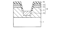
As shown in FIGS. 10 and 11, by thermal etching of
図13に示すように、SiC層10上に、ゲートトレンチGTの側壁SSを覆い底部BTを露出するマスク72が形成される。マスク72は、好ましくは、炭化珪素のエピタキシャル成長に求められる温度よりも高い融点を有する。たとえば、マスク72として炭化タンタル膜が形成される。
As shown in FIG. 13, a
図14に示すように、マスク72を用いて底部BTがエッチングされる。これにより、ゲートトレンチGTを底部BTから厚さ方向(図中、縦方向)に延長するように延びる付加トレンチATが形成される。エッチング中、マスク72によってゲートトレンチGTの側壁SSが保護される。好ましくは、このエッチングは、物理的エッチング作用を有するエッチングを用いて行われる。
As shown in FIG. 14, bottom BT is etched using
図15に示すように、付加トレンチATを埋めるように電荷補償領域14が形成される。具体的には、SiC層10を所定の加熱温度まで加熱しながら、付加トレンチAT内における炭化珪素のエピタキシャル成長が行われる。この加熱温度はマスク72の融点よりも低い。エピタキシャル成長は、たとえばCVD法によって行い得る。次にマスク72が除去される(図16)。マスク72が炭化タンタル膜を有する場合、マスク72の除去のために炭化タンタル膜の酸化が行われてもよい。
As shown in FIG. 15, the
なお電荷補償領域14は、必ずしも付加トレンチATをちょうど埋めるように形成される必要はなく、付加トレンチATとゲートトレンチGTとの境界に満たないように、またはこの境界を越えるように形成されてもよい。この場合、ゲートトレンチGTの底部BTの位置、すなわちゲート酸化膜21の底部に面するSiC層10の位置は、付加トレンチATの形成前(図13)好ましくは、電荷補償領域14は、厚さ方向DDにおいて5μmよりも大きい厚さTHを有するように形成される。
The
図17に示すように、不純物イオン注入によって、p+コンタクト領域15が形成される。次に、イオン注入により注入された不純物を活性化するための活性化アニールが行われる。たとえば1700℃の温度で30分間の加熱が行われる。 As shown in FIG. 17, ap + contact region 15 is formed by impurity ion implantation. Next, activation annealing is performed to activate the impurities implanted by ion implantation. For example, heating is performed at a temperature of 1700 ° C. for 30 minutes.
図18に示すように、SiC層10の露出面が熱酸化されることで、ゲート酸化膜21が形成される。この際、ゲートトレンチGTの内面も熱酸化されるので、ゲート酸化膜21は側壁SS上においてSiC層10のp領域12を被覆する。また底部BT上においてSiC層10の電荷補償領域14を被覆する。
As shown in FIG. 18, the exposed surface of
図19に示すように、ゲートトレンチGT内にゲート電極30が形成される。ゲート電極30は、ゲート酸化膜21を介してSiC層10のp領域12上に位置する部分を有するように形成される。
As shown in FIG. 19, the
さらに図20を参照して、まず、露出したゲート酸化膜21およびゲート電極30(図19)の上に層間絶縁膜22が形成される。次に、ゲート酸化膜21および層間絶縁膜22がパターニングされることで、p+コンタクト領域15と、n領域13の一部とを露出する開口部が形成される。次にこの開口部内にソース電極32が形成される。これにより図20に示す構成が得られる。
Further, referring to FIG. 20, first,
再び図1を参照して、層間絶縁膜22およびソース電極32の上にソース配線層33が形成される。またn-ドリフト領域11上すなわちSiC層10の下面F1上に単結晶基板1を介してドレイン電極31が形成される。以上により、MOSFET100が得られる。
Referring again to FIG. 1,
次に上記製造方法において用いられる熱エッチングについて説明する。熱エッチングとは、所定の熱処理温度まで加熱されたエッチング対象へ反応性ガスを含むプロセスガス供給することによって生じる化学反応を用いて行われるエッチングである。 Next, thermal etching used in the above manufacturing method will be described. Thermal etching is etching performed using a chemical reaction generated by supplying a process gas containing a reactive gas to an etching target heated to a predetermined heat treatment temperature.
プロセスガス中の反応性ガスとしては、塩素原子を有するガスが用いられ、好ましくは塩素系ガスが用いられ、より好ましくは塩素ガスが用いられる。また熱エッチングは、好ましくは、塩素系ガスの分圧が50%以下である雰囲気下で行われる。またプロセスガスは、好ましくは酸素原子を有するガスを含み、たとえば酸素ガスを含む。塩素ガスおよび酸素ガスが共に用いられる場合、プロセスガスの供給において、塩素ガスの流量に対する酸素ガスの流量の比率が0.1以上2.0以下となることが好ましく、より好ましくはこの比率の下限は0.25である。またプロセスガスはキャリアガスを含んでもよい。キャリアガスとしては、たとえば窒素ガス、アルゴンガス、またはヘリウムガスなどを用いることができる。また熱エッチングは、好ましくは、減圧雰囲気下で行われ、より好ましくは、減圧雰囲気は大気圧の1/10以下の圧力を有する。 As the reactive gas in the process gas, a gas having a chlorine atom is used, preferably a chlorine-based gas, more preferably a chlorine gas. The thermal etching is preferably performed in an atmosphere in which the partial pressure of the chlorine-based gas is 50% or less. The process gas preferably contains a gas having oxygen atoms, for example, oxygen gas. When both chlorine gas and oxygen gas are used, the ratio of the flow rate of oxygen gas to the flow rate of chlorine gas is preferably 0.1 or more and 2.0 or less in the supply of process gas, and more preferably the lower limit of this ratio Is 0.25. The process gas may also contain a carrier gas. As the carrier gas, for example, nitrogen gas, argon gas, helium gas, or the like can be used. The thermal etching is preferably performed in a reduced pressure atmosphere, and more preferably, the reduced pressure atmosphere has a pressure of 1/10 or less of atmospheric pressure.
また熱処理温度は、好ましくは700℃以上とされ、より好ましくは800℃以上とされ、さらに好ましくは900℃以上とされる。これによりエッチング速度を高めることができる。また熱処理温度は、好ましくは、1200℃以下とされ、より好ましくは1100℃以下とされ、さらに好ましくは1000℃以下とされる。これにより熱エッチングに用いる装置をより簡易なものとすることができ、たとえば石英部材を用いたものとすることができる。 The heat treatment temperature is preferably 700 ° C. or higher, more preferably 800 ° C. or higher, and further preferably 900 ° C. or higher. This can increase the etching rate. The heat treatment temperature is preferably 1200 ° C. or lower, more preferably 1100 ° C. or lower, and further preferably 1000 ° C. or lower. Thereby, the apparatus used for thermal etching can be simplified, and for example, a quartz member can be used.
熱エッチングのマスク層71(図11)は、酸化珪素から作られることが好ましい。これによりエッチング中のマスクの消耗を抑制することができる。 The thermal etching mask layer 71 (FIG. 11) is preferably made of silicon oxide. Thereby, the consumption of the mask during etching can be suppressed.
上記のような熱エッチングによって、ゲートトレンチGTの側壁SS(図2)として、化学的安定性の高い、結晶学的に特定の結晶面を自己形成することができる。形成される結晶面は、SiC層10の結晶構造が六方晶系の場合、{0−33−8}面または{01−1−4}面の少なくともいずれかを含み得る。またその結晶構造が立方晶系である場合には、その結晶面は{100}面を含み得る。
By thermal etching as described above, a crystallographically specific crystal plane having high chemical stability can be self-formed as the sidewall SS (FIG. 2) of the gate trench GT. When the crystal structure of the
次にMOSFET100(図1)の使用方法と、本実施の形態における作用効果とについて、以下に説明する。 Next, a method of using MOSFET 100 (FIG. 1) and the operation and effect of the present embodiment will be described below.
MOSFET100は、ドレイン電極31とソース配線層33との間の電流経路のスイッチングを行うスイッチング素子として用いられる。ドレイン電極31にはソース配線層33に対して正の電圧が印加される。ゲート電極30にしきい値以上の正の電圧が印加されている場合、ゲートトレンチGTの側壁SS上におけるp領域12、すなわちチャネル領域に、反転層が存在する。よって、n-ドリフト領域11とn領域13とは電気的に接続された状態であり、MOSFET100はオン状態である。
The
ゲート電極30へのしきい値以上の電圧の印加が停止されると、上記反転層が消失するので、ソース配線層33からn-ドリフト領域11中へのキャリアの供給が停止される。その結果、n-ドリフト領域11およびp領域12によるpn接合面からドレイン電極31の方へ、空乏化が進行する。この結果、n-ドリフト領域11および電荷補償領域14が空乏化される。
When the application of a voltage equal to or higher than the threshold value to the
空乏化されたn-ドリフト領域11が有する正の固定電荷は、上記pn接合面上での厚さ方向における電界強度を高める要因となる。一方、空乏化された電荷補償領域14は負の固定電荷を有するので、この負の固定電荷が、上記電界強度の少なくとも一部を相殺する。すなわち電荷補償領域14が電荷補償構造として機能する。これにより厚さ方向の電界強度の最大値が抑制される。よってMOSFET100の耐圧を向上させることができる。より好ましくは上記相殺が完全に行われる。この場合、電荷補償構造中での総電荷がゼロとなることで、電荷補償構造中での厚さ方向の電界の傾きもゼロとなるので、より高い耐圧が得られる。
The positive fixed charge of the depleted n − drift region 11 becomes a factor for increasing the electric field strength in the thickness direction on the pn junction surface. On the other hand, since the depleted
電荷補償領域14は、厚さ方向DD(図2)において好ましくは5μmよりも大きい厚さTHを有する。これにより電荷補償構造が、厚さ方向DDにおいてより広い範囲にわたって設けられる。よってMOSFET100の耐圧をより向上させることができる。厚さTHが5μmよりも大きい場合、アバランチェ耐圧をおおよそ500V以上とし得る。
The
また付加トレンチATのエッチングに用いられるマスク72(図13および図14)は、電荷補償領域14が形成された後に除去される。これにより電荷補償領域14を形成するための成膜の際に生じた不必要な部分をマスク72と共に除去することができる。具体的には、単結晶炭化珪素からなる電荷補償領域14の形成時にマスク72上に生じたアモルファス炭化珪素が除去される。
The mask 72 (FIGS. 13 and 14) used for etching the additional trench AT is removed after the
付加トレンチATの形成の際に、好ましくは、物理的エッチング作用を有するエッチングが用いられる。これにより、付加トレンチATの形成のためのエッチングを、より垂直に行うことができる。これにより、付加トレンチAT内に形成される電荷補償領域14の側面SD(図2)を厚さ方向DDに沿わせることができる。よって電荷補償領域14による電荷補償をより十分に行うことができる。
In forming the additional trench AT, preferably, etching having a physical etching action is used. Thereby, the etching for forming the additional trench AT can be performed more vertically. As a result, the side surface SD (FIG. 2) of the
また本実施の形態においては、ゲートトレンチGTが形成される際に熱エッチングが用いられる。これによりゲートトレンチGTの側壁SSの面方位を結晶学的に特定のものに自己形成することができる。好ましくは、ゲートトレンチGTの側壁SSはSiC層10の上面F2に対して、0°よりも大きく90°よりも小さい角度AF(図2)だけ傾斜している。これによりゲートトレンチGTの側壁SS上に、上面F2に対して傾いた面方位を有するチャネル面を設けることができる。より好ましくは、厚さ方向DDに対する電荷補償領域14の側面SD(図2)の角度は、厚さ方向DDに対するゲートトレンチGTの角度ADに比して小さい。これにより、電荷補償領域14による電荷補償をより十分に行うことができる。
In the present embodiment, thermal etching is used when the gate trench GT is formed. Thereby, the plane orientation of the side wall SS of the gate trench GT can be self-formed in a crystallographically specific one. Preferably, side wall SS of gate trench GT is inclined with respect to upper surface F2 of
SiC層10は六方晶系の結晶構造を有してもよく、この場合、SiC層10のゲートトレンチGTの側壁SSは{0−33−8}面および{0−11−4}面の少なくともいずれかからなる部分を含むことが好ましい。これにより、側壁SS上におけるキャリア移動度を高めることができる。よってMOSFET100のオン抵抗を抑制することができる。
The
SiC層10は立方晶系の結晶構造を有してもよく、この場合、SiC層10のゲートトレンチGTの側壁SSは{100}面からなる部分を含むことが好ましい。これにより、側壁SS上におけるキャリア移動度を高めることができる。よってMOSFET100のオン抵抗を抑制することができる。
またMOSFET100の製造方法において、ドレイン電極31(図1)を形成する前に、単結晶基板1を薄くする工程が行われてもよい。極端な場合、単結晶基板1が除去されてもよく、この場合、MOSFET100(図1)は単結晶基板1を有さず、ドレイン電極31は、n-ドリフト領域11上、すなわち下面F1上に直接に設けられる。
In the method for manufacturing
またゲートトレンチGTは熱エッチング以外のドライエッチングによって形成されてもよく、たとえばRIEまたはIBEによって形成されてもよい。またゲートトレンチGTはドライエッチング以外のエッチングによって形成されてもよく、たとえばウエットエッチングによって形成されてもよい。またゲートトレンチの互いに対向する側壁は、図1に示すような非平行な位置関係を必ずしも有する必要はなく、互いに平行な関係を有してもよい。 The gate trench GT may be formed by dry etching other than thermal etching, and may be formed by, for example, RIE or IBE. The gate trench GT may be formed by etching other than dry etching, for example, wet etching. Further, the side walls facing each other of the gate trench are not necessarily required to have a non-parallel positional relationship as shown in FIG. 1, but may have a parallel relationship.
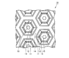
また上記実施の形態においては、図4に示すように、上面F2の、ゲートトレンチGTの側壁SSに囲まれた部分は六角形の形状を有する。この部分の形状は六角形の形状に限定されるものではなく、たとえば長方形(正方形を含む)であってもよい。またこの形状は、SiC層10の結晶構造が六方晶の場合は各角が約60°の角度を有する六角形が好ましく、立方晶の場合は長方形が好ましい。
Moreover, in the said embodiment, as shown in FIG. 4, the part enclosed by the side wall SS of the gate trench GT of the upper surface F2 has a hexagonal shape. The shape of this portion is not limited to a hexagonal shape, and may be, for example, a rectangle (including a square). This shape is preferably a hexagon having an angle of about 60 ° when the crystal structure of the
また第1導電型はn型に限定されるものではなく、p型であってもよい。MOSFETは、第1導電型がn型の場合はnチャネル型であり、p型の場合はpチャネル型である。 The first conductivity type is not limited to n-type, and may be p-type. The MOSFET is n-channel type when the first conductivity type is n-type, and p-channel type when the first conductivity type is p-type.
また炭化珪素半導体装置はMOSFETに限定されるものではなく、たとえばMOSFET以外のMISFET(Metal Insulator Semiconductor Field Effect Transistor)であってもよい。 The silicon carbide semiconductor device is not limited to a MOSFET, and may be, for example, a MISFET (Metal Insulator Semiconductor Field Effect Transistor) other than a MOSFET.
今回開示された実施の形態はすべての点で例示であって制限的なものではないと考えられるべきである。本発明の特許請求の範囲は上記した説明ではなくて請求の範囲によって示され、特許請求の範囲と均等の意味および範囲内でのすべての変更が含まれることが意図される。 The embodiment disclosed this time should be considered as illustrative in all points and not restrictive. The scope of the claims of the present invention is defined by the terms of the claims, rather than the description above, and is intended to include any modifications within the scope and meaning equivalent to the terms of the claims.
1 単結晶基板、10 SiC層(炭化珪素層)、11 n-ドリフト領域(第1領域)、12 p領域(第2領域)、13 n領域(第3領域)、14 電荷補償領域、15 p+コンタクト領域、21 ゲート酸化膜(ゲート絶縁膜)、22 層間絶縁膜、30 ゲート電極、31 ドレイン電極(第1電極)、32 ソース電極(第2電極)、33 ソース配線層、71 マスク層、72 マスク、100 MOSFET(炭化珪素半導体装置)、AT 付加トレンチ、BT 底部、F1 下面(第1表面)、F2 上面(第2表面)、GT ゲートトレンチ、SD 側面、SS 側壁。 Single crystal substrate, 10 SiC layer (silicon carbide layer), 11 n - drift region (first region), 12 p region (second region), 13 n region (third region), 14 charge compensation region, 15 p + Contact region, 21 gate oxide film (gate insulating film), 22 interlayer insulating film, 30 gate electrode, 31 drain electrode (first electrode), 32 source electrode (second electrode), 33 source wiring layer, 71 mask layer, 72 mask, 100 MOSFET (silicon carbide semiconductor device), AT additional trench, BT bottom, F1 bottom surface (first surface), F2 top surface (second surface), GT gate trench, SD side surface, SS side wall.
Claims (14)
前記第2表面に、前記第3領域および前記第2領域を貫通して前記第1領域に至り底部および側壁を有するゲートトレンチを形成する工程を備え、前記側壁は前記第1領域と前記第2領域と前記第3領域との各々からなる部分を有し、さらに
前記ゲートトレンチを前記底部から前記厚さ方向に延長するように延びる付加トレンチを形成する工程と、
前記付加トレンチを埋めるように、前記第2導電型を有する第4領域を形成する工程と、
前記側壁上において前記炭化珪素層の前記第2領域を被覆するゲート絶縁膜を形成する工程と、
前記ゲート絶縁膜を介して前記炭化珪素層の前記第2領域上にゲート電極を形成する工程と、
前記炭化珪素層の前記第1領域上に第1電極を形成する工程と、
前記炭化珪素層の前記第3領域上に第2電極を形成する工程とを備える、炭化珪素半導体装置の製造方法。 Providing a silicon carbide layer having a first surface and a second surface facing each other in the thickness direction, wherein the silicon carbide layer includes the first region having the first surface and the first conductivity type; A second region provided on the first region and having a second conductivity type different from the first conductivity type so as to be separated from the first surface by the first region; and the second region provided on the second region. A third region separated from the first region by the region and having the first conductivity type, and further, the second surface penetrates the third region and the second region to reach the first region and reaches the bottom. And a step of forming a gate trench having a side wall, the side wall having a portion comprising each of the first region, the second region, and the third region, and further, the gate trench from the bottom to the thickness. I will extend in the direction Forming an additional trench extending,
Forming a fourth region having the second conductivity type so as to fill the additional trench;
Forming a gate insulating film covering the second region of the silicon carbide layer on the sidewall;
Forming a gate electrode on the second region of the silicon carbide layer via the gate insulating film;
Forming a first electrode on the first region of the silicon carbide layer;
Forming a second electrode on the third region of the silicon carbide layer.
前記炭化珪素層上に、前記ゲートトレンチの前記側壁を覆い前記底部を露出するマスクを形成する工程と、
前記マスクを用いて前記底部をエッチングする工程とを含む、請求項1または2に記載の炭化珪素半導体装置の製造方法。 The step of forming the additional trench includes:
Forming a mask covering the sidewall of the gate trench and exposing the bottom on the silicon carbide layer;
The method for manufacturing a silicon carbide semiconductor device according to claim 1, further comprising: etching the bottom using the mask.
前記マスクは前記加熱温度よりも高い融点を有する、請求項4に記載の炭化珪素半導体装置の製造方法。 The step of forming the fourth region includes the step of heating the silicon carbide layer to a heating temperature,
The method for manufacturing a silicon carbide semiconductor device according to claim 4, wherein the mask has a melting point higher than the heating temperature.
前記側壁上において前記炭化珪素層の前記第2領域を被覆するゲート絶縁膜と、
前記ゲート絶縁膜を介して前記炭化珪素層の前記第2領域上に設けられたゲート電極と、
前記炭化珪素層の前記第1領域上に設けられた第1電極と、
前記炭化珪素層の前記第3領域上に設けられた第2電極とを備える、炭化珪素半導体装置。 A silicon carbide layer having a first surface and a second surface opposed to each other in the thickness direction, wherein the silicon carbide layer includes a first region having the first surface and having a first conductivity type, and the first region; A second region having a second conductivity type different from the first conductivity type provided on the first region so as to be separated from the first surface; and the second region provided on the second region by the second region. And a third region having the first conductivity type separated from the first region, the gate having the bottom surface and the side wall penetrating through the third region and the second region to the first region on the second surface. A trench is provided, and the side wall has a portion composed of each of the first region, the second region, and the third region, and the silicon carbide layer is provided at the bottom and is formed by the first region. Separated from the first surface and the second A gate insulating film including a fourth region having an electric type, wherein the fourth region has a thickness greater than 5 μm in the thickness direction, and further covers the second region of the silicon carbide layer on the sidewall When,
A gate electrode provided on the second region of the silicon carbide layer via the gate insulating film;
A first electrode provided on the first region of the silicon carbide layer;
A silicon carbide semiconductor device comprising: a second electrode provided on the third region of the silicon carbide layer.
Priority Applications (4)
| Application Number | Priority Date | Filing Date | Title |
|---|---|---|---|
| JP2012031389A JP2013168540A (en) | 2012-02-16 | 2012-02-16 | Silicon carbide semiconductor device manufacturing method and silicon carbide semiconductor device |
| DE102013200046A DE102013200046A1 (en) | 2012-02-16 | 2013-01-03 | A method of manufacturing a silicon carbide semiconductor device and silicon carbide semiconductor device |
| US13/738,636 US20130214290A1 (en) | 2012-02-16 | 2013-01-10 | Method for manufacturing silicon carbide semiconductor device and silicon carbide semiconductor device |
| CN2013100163771A CN103258721A (en) | 2012-02-16 | 2013-01-16 | Method for manufacturing silicon carbide semiconductor device and silicon carbide semiconductor device |
Applications Claiming Priority (1)
| Application Number | Priority Date | Filing Date | Title |
|---|---|---|---|
| JP2012031389A JP2013168540A (en) | 2012-02-16 | 2012-02-16 | Silicon carbide semiconductor device manufacturing method and silicon carbide semiconductor device |
Publications (1)
| Publication Number | Publication Date |
|---|---|
| JP2013168540A true JP2013168540A (en) | 2013-08-29 |
Family
ID=48915356
Family Applications (1)
| Application Number | Title | Priority Date | Filing Date |
|---|---|---|---|
| JP2012031389A Pending JP2013168540A (en) | 2012-02-16 | 2012-02-16 | Silicon carbide semiconductor device manufacturing method and silicon carbide semiconductor device |
Country Status (4)
| Country | Link |
|---|---|
| US (1) | US20130214290A1 (en) |
| JP (1) | JP2013168540A (en) |
| CN (1) | CN103258721A (en) |
| DE (1) | DE102013200046A1 (en) |
Cited By (2)
| Publication number | Priority date | Publication date | Assignee | Title |
|---|---|---|---|---|
| JP2015191923A (en) * | 2014-03-27 | 2015-11-02 | 住友電気工業株式会社 | Silicon carbide semiconductor device and manufacturing method thereof |
| WO2016204112A1 (en) * | 2015-06-18 | 2016-12-22 | 住友電気工業株式会社 | Silicon carbide semiconductor device and production method for same |
Families Citing this family (12)
| Publication number | Priority date | Publication date | Assignee | Title |
|---|---|---|---|---|
| US9006798B2 (en) * | 2013-05-03 | 2015-04-14 | Infineon Technologies Ag | Semiconductor device including trench transistor cell array and manufacturing method |
| US9496339B2 (en) * | 2014-06-02 | 2016-11-15 | Infineon Technologies Austria Ag | Semiconductor device comprising trench structures |
| CN106158650A (en) * | 2015-04-16 | 2016-11-23 | 中芯国际集成电路制造(上海)有限公司 | Transistor and forming method thereof |
| TWI646653B (en) * | 2017-12-28 | 2019-01-01 | 新唐科技股份有限公司 | Laterally diffused metal oxide semiconductor field effect transistor |
| JP7210182B2 (en) * | 2018-07-26 | 2023-01-23 | 株式会社東芝 | Semiconductor devices, inverter circuits, drive devices, vehicles, and elevators |
| CN111354793B (en) * | 2018-12-21 | 2023-03-14 | 比亚迪半导体股份有限公司 | Field effect transistor, preparation method and electronic equipment |
| CN110350035A (en) * | 2019-05-30 | 2019-10-18 | 上海功成半导体科技有限公司 | SiC MOSFET power device and preparation method thereof |
| US12295158B2 (en) * | 2019-12-20 | 2025-05-06 | Sumitomo Electric Industries, Ltd. | Silicon carbide semiconductor device |
| JP7686594B2 (en) * | 2022-03-22 | 2025-06-02 | 株式会社東芝 | Semiconductor device, inverter circuit, drive device, vehicle, and elevator |
| CN115763524B (en) * | 2022-11-22 | 2025-10-17 | 中国科学院苏州纳米技术与纳米仿生研究所 | Vertical enhancement beta-Ga2O3UMOSFET device and preparation method thereof |
| CN117457748B (en) * | 2023-12-22 | 2024-05-28 | 深圳天狼芯半导体有限公司 | A SiC super junction MOS with a P-type space layer under the gate and a preparation method thereof |
| CN117497602B (en) * | 2023-12-29 | 2024-04-19 | 深圳天狼芯半导体有限公司 | A split-gate trench MOSFET and its preparation method and chip |
Family Cites Families (7)
| Publication number | Priority date | Publication date | Assignee | Title |
|---|---|---|---|---|
| JP2004342660A (en) | 2003-05-13 | 2004-12-02 | Toshiba Corp | Semiconductor device and manufacturing method thereof |
| US20060211210A1 (en) * | 2004-08-27 | 2006-09-21 | Rensselaer Polytechnic Institute | Material for selective deposition and etching |
| US7595241B2 (en) * | 2006-08-23 | 2009-09-29 | General Electric Company | Method for fabricating silicon carbide vertical MOSFET devices |
| JP4640439B2 (en) * | 2008-04-17 | 2011-03-02 | 株式会社デンソー | Silicon carbide semiconductor device |
| CN102396070A (en) * | 2009-04-13 | 2012-03-28 | 罗姆股份有限公司 | Semiconductor device and method for manufacturing semiconductor device |
| US8415671B2 (en) * | 2010-04-16 | 2013-04-09 | Cree, Inc. | Wide band-gap MOSFETs having a heterojunction under gate trenches thereof and related methods of forming such devices |
| JP5558392B2 (en) * | 2011-03-10 | 2014-07-23 | 株式会社東芝 | Semiconductor device and manufacturing method thereof |
-
2012
- 2012-02-16 JP JP2012031389A patent/JP2013168540A/en active Pending
-
2013
- 2013-01-03 DE DE102013200046A patent/DE102013200046A1/en not_active Withdrawn
- 2013-01-10 US US13/738,636 patent/US20130214290A1/en not_active Abandoned
- 2013-01-16 CN CN2013100163771A patent/CN103258721A/en active Pending
Cited By (3)
| Publication number | Priority date | Publication date | Assignee | Title |
|---|---|---|---|---|
| JP2015191923A (en) * | 2014-03-27 | 2015-11-02 | 住友電気工業株式会社 | Silicon carbide semiconductor device and manufacturing method thereof |
| WO2016204112A1 (en) * | 2015-06-18 | 2016-12-22 | 住友電気工業株式会社 | Silicon carbide semiconductor device and production method for same |
| JP2017011031A (en) * | 2015-06-18 | 2017-01-12 | 住友電気工業株式会社 | Silicon carbide semiconductor device and manufacturing method thereof |
Also Published As
| Publication number | Publication date |
|---|---|
| US20130214290A1 (en) | 2013-08-22 |
| DE102013200046A1 (en) | 2013-08-22 |
| CN103258721A (en) | 2013-08-21 |
Similar Documents
| Publication | Publication Date | Title |
|---|---|---|
| JP2013168540A (en) | Silicon carbide semiconductor device manufacturing method and silicon carbide semiconductor device | |
| US8941121B2 (en) | Silicon carbide semiconductor device and method for manufacturing silicon carbide semiconductor device | |
| JP5668576B2 (en) | Silicon carbide semiconductor device | |
| CN103782391B (en) | Silicon carbide semiconductor device and manufacturing method thereof | |
| US8415241B2 (en) | Method of manufacturing silicon carbide semiconductor device | |
| CN103765594B (en) | Sic semiconductor device | |
| JP2012164707A (en) | Semiconductor device, and method of manufacturing the same | |
| JP6991476B2 (en) | Semiconductor device | |
| JP6171678B2 (en) | Silicon carbide semiconductor device and manufacturing method thereof | |
| JP5867134B2 (en) | Method for manufacturing silicon carbide semiconductor device | |
| JP6135383B2 (en) | Silicon carbide semiconductor device | |
| JP5880311B2 (en) | Silicon carbide semiconductor device | |
| JP6256075B2 (en) | Silicon carbide semiconductor device | |
| JPWO2018096722A1 (en) | Semiconductor device | |
| JP6233436B2 (en) | Method for manufacturing silicon carbide semiconductor device | |
| JP2014033031A (en) | Silicon carbide semiconductor device and method of manufacturing the same | |
| JP2013172119A (en) | Silicon carbide semiconductor device and manufacturing method therefor |