JP2013148444A - Terahertz camera and electronic apparatus - Google Patents
Terahertz camera and electronic apparatus Download PDFInfo
- Publication number
- JP2013148444A JP2013148444A JP2012008714A JP2012008714A JP2013148444A JP 2013148444 A JP2013148444 A JP 2013148444A JP 2012008714 A JP2012008714 A JP 2012008714A JP 2012008714 A JP2012008714 A JP 2012008714A JP 2013148444 A JP2013148444 A JP 2013148444A
- Authority
- JP
- Japan
- Prior art keywords
- electromagnetic wave
- pyroelectric
- detection element
- wave absorber
- reflector
- Prior art date
- Legal status (The legal status is an assumption and is not a legal conclusion. Google has not performed a legal analysis and makes no representation as to the accuracy of the status listed.)
- Pending
Links
- 238000001514 detection method Methods 0.000 claims abstract description 82
- 239000006096 absorbing agent Substances 0.000 claims abstract description 59
- 239000003990 capacitor Substances 0.000 claims abstract description 41
- 230000010287 polarization Effects 0.000 claims abstract description 5
- 238000005192 partition Methods 0.000 claims description 15
- 239000000463 material Substances 0.000 claims description 9
- 239000010410 layer Substances 0.000 description 100
- 239000010408 film Substances 0.000 description 69
- 230000004888 barrier function Effects 0.000 description 45
- 239000007789 gas Substances 0.000 description 36
- 238000005530 etching Methods 0.000 description 33
- 238000004519 manufacturing process Methods 0.000 description 17
- 239000011229 interlayer Substances 0.000 description 16
- 238000000034 method Methods 0.000 description 16
- 238000000277 atomic layer chemical vapour deposition Methods 0.000 description 14
- 238000012545 processing Methods 0.000 description 14
- 229910052751 metal Inorganic materials 0.000 description 10
- 239000002184 metal Substances 0.000 description 10
- 230000003287 optical effect Effects 0.000 description 9
- 229910018072 Al 2 O 3 Inorganic materials 0.000 description 8
- 238000010521 absorption reaction Methods 0.000 description 8
- TWNQGVIAIRXVLR-UHFFFAOYSA-N oxo(oxoalumanyloxy)alumane Chemical compound O=[Al]O[Al]=O TWNQGVIAIRXVLR-UHFFFAOYSA-N 0.000 description 8
- KRHYYFGTRYWZRS-UHFFFAOYSA-N Fluorane Chemical compound F KRHYYFGTRYWZRS-UHFFFAOYSA-N 0.000 description 6
- 229910004298 SiO 2 Inorganic materials 0.000 description 6
- 230000015572 biosynthetic process Effects 0.000 description 6
- 238000003384 imaging method Methods 0.000 description 6
- 230000008569 process Effects 0.000 description 6
- 239000000126 substance Substances 0.000 description 6
- 238000006243 chemical reaction Methods 0.000 description 5
- 238000005229 chemical vapour deposition Methods 0.000 description 5
- 230000006870 function Effects 0.000 description 5
- 238000004544 sputter deposition Methods 0.000 description 5
- 238000012546 transfer Methods 0.000 description 5
- 238000005304 joining Methods 0.000 description 4
- 230000001681 protective effect Effects 0.000 description 4
- 239000000758 substrate Substances 0.000 description 4
- 238000011144 upstream manufacturing Methods 0.000 description 4
- UFHFLCQGNIYNRP-UHFFFAOYSA-N Hydrogen Chemical compound [H][H] UFHFLCQGNIYNRP-UHFFFAOYSA-N 0.000 description 3
- XUIMIQQOPSSXEZ-UHFFFAOYSA-N Silicon Chemical compound [Si] XUIMIQQOPSSXEZ-UHFFFAOYSA-N 0.000 description 3
- RTAQQCXQSZGOHL-UHFFFAOYSA-N Titanium Chemical compound [Ti] RTAQQCXQSZGOHL-UHFFFAOYSA-N 0.000 description 3
- 238000000151 deposition Methods 0.000 description 3
- 230000000694 effects Effects 0.000 description 3
- 239000001257 hydrogen Substances 0.000 description 3
- 229910052739 hydrogen Inorganic materials 0.000 description 3
- 238000005259 measurement Methods 0.000 description 3
- 238000012986 modification Methods 0.000 description 3
- 230000004048 modification Effects 0.000 description 3
- 229910052710 silicon Inorganic materials 0.000 description 3
- 239000010703 silicon Substances 0.000 description 3
- 125000006850 spacer group Chemical group 0.000 description 3
- 239000010936 titanium Substances 0.000 description 3
- 229910052719 titanium Inorganic materials 0.000 description 3
- 238000010586 diagram Methods 0.000 description 2
- 238000007689 inspection Methods 0.000 description 2
- 230000010354 integration Effects 0.000 description 2
- 230000015654 memory Effects 0.000 description 2
- 230000002269 spontaneous effect Effects 0.000 description 2
- 238000003860 storage Methods 0.000 description 2
- 239000010409 thin film Substances 0.000 description 2
- XLYOFNOQVPJJNP-UHFFFAOYSA-N water Chemical compound O XLYOFNOQVPJJNP-UHFFFAOYSA-N 0.000 description 2
- 229910010037 TiAlN Inorganic materials 0.000 description 1
- 239000011358 absorbing material Substances 0.000 description 1
- 230000009471 action Effects 0.000 description 1
- 229910052782 aluminium Inorganic materials 0.000 description 1
- XAGFODPZIPBFFR-UHFFFAOYSA-N aluminium Chemical compound [Al] XAGFODPZIPBFFR-UHFFFAOYSA-N 0.000 description 1
- 238000000137 annealing Methods 0.000 description 1
- QVGXLLKOCUKJST-UHFFFAOYSA-N atomic oxygen Chemical compound [O] QVGXLLKOCUKJST-UHFFFAOYSA-N 0.000 description 1
- 230000001066 destructive effect Effects 0.000 description 1
- 238000009826 distribution Methods 0.000 description 1
- 239000003814 drug Substances 0.000 description 1
- 238000005516 engineering process Methods 0.000 description 1
- 230000017525 heat dissipation Effects 0.000 description 1
- 150000002431 hydrogen Chemical class 0.000 description 1
- 125000002887 hydroxy group Chemical group [H]O* 0.000 description 1
- 238000003702 image correction Methods 0.000 description 1
- 230000001771 impaired effect Effects 0.000 description 1
- 230000006872 improvement Effects 0.000 description 1
- 239000004973 liquid crystal related substance Substances 0.000 description 1
- 125000002496 methyl group Chemical group [H]C([H])([H])* 0.000 description 1
- 150000004767 nitrides Chemical class 0.000 description 1
- 239000001301 oxygen Substances 0.000 description 1
- 229910052760 oxygen Inorganic materials 0.000 description 1
- 238000000059 patterning Methods 0.000 description 1
- 238000000206 photolithography Methods 0.000 description 1
- 239000007787 solid Substances 0.000 description 1
- 230000003595 spectral effect Effects 0.000 description 1
- 238000001228 spectrum Methods 0.000 description 1
Images


Landscapes
- Photometry And Measurement Of Optical Pulse Characteristics (AREA)
- Transforming Light Signals Into Electric Signals (AREA)
Abstract
【課題】電磁波吸収体に直接入射されない電磁波も、電磁波検出に寄与させて検出精度を向上できるテラヘルツカメラおよび電子機器を提供すること。
【解決手段】焦電型検出器200は、焦電型検出素子220と、電磁波吸収体270と、支持部材210と、支持部100,104と、反射体160とを有する。支持部材210に支持される焦電型検出素子220は、温度に基づいて分極量が変化するキャパシター230を含む。電磁波吸収体270は、焦電型検出素子の頂部を覆い、平面視にてキャパシターの面積よりも広い面積を有する。反射体160は、焦電型検出素子の周囲に配置され、入射された電磁波を電磁波吸収体に向けて反射させる。
【選択図】図1To provide a terahertz camera and an electronic device capable of improving detection accuracy by making electromagnetic waves not directly incident on an electromagnetic wave absorber contribute to electromagnetic wave detection.
A pyroelectric detector 200 includes a pyroelectric detection element 220, an electromagnetic wave absorber 270, a support member 210, support portions 100 and 104, and a reflector 160. The pyroelectric detection element 220 supported by the support member 210 includes a capacitor 230 whose polarization amount changes based on temperature. The electromagnetic wave absorber 270 covers the top of the pyroelectric detection element and has an area larger than the area of the capacitor in plan view. The reflector 160 is disposed around the pyroelectric detection element, and reflects incident electromagnetic waves toward the electromagnetic wave absorber.
[Selection] Figure 1
Description
本発明は、テラヘルツカメラおよび電子機器に関する。 The present invention relates to a terahertz camera and an electronic apparatus.
テラヘルツ波は、波長が赤外線に近い電磁波である。このテラヘルツ波を用いた画像計測技術は各種方面への活用が研究されている。例えば、テラヘルツカメラによる特定物質探知装置、偽造紙幣の判定、封筒内の薬品検出、建造物の非破壊検査等がある。
一方、赤外線カメラとしては、焦電型検出器を用いるカメラがある。出願人は、テラヘルツ波の波長が赤外線に近いことから、テラヘルツカメラに焦電型検出器を用いる技術を発明した。
A terahertz wave is an electromagnetic wave having a wavelength close to infrared. The image measurement technology using terahertz waves has been studied for use in various fields. For example, there are a specific substance detection device using a terahertz camera, determination of counterfeit bills, detection of chemicals in envelopes, non-destructive inspection of buildings, and the like.
On the other hand, as an infrared camera, there is a camera using a pyroelectric detector. The applicant has invented a technique of using a pyroelectric detector in a terahertz camera because the wavelength of the terahertz wave is close to infrared.
焦電型検出装置のセルは、上部電極と下部電極とに接続された焦電体を含むキャパシターを有し、電極や焦電体の材料に関して、各種の提案がなされている(特許文献1)。 The cell of the pyroelectric detection device has a capacitor including a pyroelectric body connected to an upper electrode and a lower electrode, and various proposals have been made regarding materials of the electrode and the pyroelectric body (Patent Document 1). .
また、上部電極と下部電極とに接続された強誘電体を含むキャパシターは強誘電体メモリーに用いられており、強誘電体メモリーに適した電極や強誘電体の材料に関しても、各種の提案がなされている(特許文献2,3)。ボロメーター型検出器として、特許文献4には電磁波を吸収する構造が開示されている。 Capacitors including ferroelectrics connected to the upper and lower electrodes are used in ferroelectric memories, and various proposals have been made regarding electrodes suitable for ferroelectric memories and ferroelectric materials. (Patent Documents 2 and 3). As a bolometer-type detector, Patent Document 4 discloses a structure that absorbs electromagnetic waves.
焦電型でもボロメーター型でも、電磁波検出装置では入射された電磁波を効率よく吸収して得た熱を検出素子に効率よく伝達することが、測定精度の向上につながる。ボロメーター型検出装置を開示した特許文献4の図21及び図22では、ボロメーター薄膜を含む検出部の裏面側にて空洞部を介して反射膜が配置され、検出部と反射膜との距離をλ/4(λは入射波長)として光学的共振構造としている。また、特許文献の図1等では、検出部よりも電磁波入射側に平板状の電磁波吸収部を設け、検出部と電磁波吸収部とを接合柱にて連結している。 In both the pyroelectric type and the bolometer type, in the electromagnetic wave detection device, efficiently transferring the heat obtained by efficiently absorbing the incident electromagnetic wave to the detection element leads to an improvement in measurement accuracy. In FIG. 21 and FIG. 22 of Patent Document 4 that discloses a bolometer-type detection device, a reflective film is disposed on the back side of the detection unit including the bolometer thin film via a cavity, and the distance between the detection unit and the reflection film Is λ / 4 (λ is an incident wavelength) to form an optical resonance structure. Moreover, in FIG. 1 etc. of patent document, the flat electromagnetic wave absorption part is provided in the electromagnetic wave incident side rather than the detection part, and the detection part and the electromagnetic wave absorption part are connected with the joining pillar.
特許文献4の技術を焦電型検出器に応用すると、焦電型検出素子は2つの電極間に焦電材料を挟んだキャパシター構造を有するので、キャパシターの裏側の反射膜に電磁波はほとんど到達せず、むしろキャパシター中の電極で反射されてしまう。 When the technique of Patent Document 4 is applied to a pyroelectric detector, the pyroelectric detection element has a capacitor structure in which a pyroelectric material is sandwiched between two electrodes, so that almost no electromagnetic wave reaches the reflective film on the back side of the capacitor. Rather, it is reflected by the electrode in the capacitor.
また、検出部と電磁波吸収部とを接合柱にて連結すると、垂直に起立する接合柱は電磁波の吸収にほとんど寄与せず、しかも電磁波吸収部と検出部との間の唯一の伝熱経路である接合柱の横断面積が小さいために伝熱性も劣り、伝熱損失が生ずる。しかも、電磁波吸収膜に直接入射されない電磁波は、検出に寄与させることができない。 In addition, when the detection unit and the electromagnetic wave absorption unit are connected by a joining column, the vertical connection column hardly contributes to the absorption of the electromagnetic wave and is the only heat transfer path between the electromagnetic wave absorption unit and the detection unit. Since the cross-sectional area of a certain connecting column is small, the heat transfer property is inferior and heat transfer loss occurs. Moreover, electromagnetic waves that are not directly incident on the electromagnetic wave absorbing film cannot contribute to detection.
本発明の幾つかの態様では、焦電型検出素子よりも電磁波入射方向の上流側に配置され電磁波吸収体に直接入射されない電磁波も、電磁波検出に寄与させて検出精度を向上できるテラヘルツカメラおよび電子機器を提供することにある。 In some aspects of the present invention, an electromagnetic wave that is disposed upstream of the pyroelectric detection element in the electromagnetic wave incident direction and that is not directly incident on the electromagnetic wave absorber also contributes to electromagnetic wave detection and can improve detection accuracy. To provide equipment.
本発明の一態様に係るテラヘルツカメラは、
第1電極と、第2電極と、前記第1,第2電極間に配置された焦電材料とから成り、温度に基づいて分極量が変化するキャパシターを含む焦電型検出素子と、
前記焦電型検出素子の頂部を覆い、かつ、前記焦電型検出素子の頂部より外側に張り出して平板状に形成され、平面視にて前記キャパシターの面積よりも広い面積を有する電磁波吸収体と、
第1面と、前記第1面に対向する第2面とを含み、前記第2面が空洞部に臨んで配置され、前記第1面が前記第1電極と接して前記焦電型検出素子を搭載する支持部材と、
前記支持部材の前記第2面の一部を支持する支持部と、
前記焦電型検出素子の周囲に配置され、入射された電磁波を前記電磁波吸収体に向けて反射させる反射体と、
を有することを特徴とする。
A terahertz camera according to one embodiment of the present invention is provided.
A pyroelectric detection element including a first electrode, a second electrode, and a pyroelectric material disposed between the first and second electrodes, and including a capacitor whose polarization amount changes based on temperature;
An electromagnetic wave absorber that covers a top portion of the pyroelectric detection element and projects outward from the top portion of the pyroelectric detection element, is formed in a flat plate shape, and has an area larger than the area of the capacitor in plan view; ,
The pyroelectric detection element includes a first surface and a second surface facing the first surface, the second surface facing the cavity, and the first surface is in contact with the first electrode A support member for mounting
A support part for supporting a part of the second surface of the support member;
A reflector disposed around the pyroelectric detection element and reflecting an incident electromagnetic wave toward the electromagnetic wave absorber;
It is characterized by having.
本発明の一態様によれば、焦電型検出素子よりも電磁波入射方向の上流側に配置された電磁波吸収体に電磁波が入射されることで、電磁波吸収体が発熱し、その熱が電磁波吸収体よりキャパシターに伝熱され、焦電効果により吸収される電磁波量に応じた電気信号を取り出すことができる。電磁波吸収体に直接入射されない電磁波も、焦電型検出素子の周囲に配置された反射体により反射されて電磁波吸収体に入射されるので、吸収される電磁波量を増大させることができ、それにより信号検出精度が向上する。 According to one aspect of the present invention, when an electromagnetic wave is incident on an electromagnetic wave absorber disposed upstream of the pyroelectric detection element in the electromagnetic wave incident direction, the electromagnetic wave absorber generates heat, and the heat is absorbed by the electromagnetic wave. An electric signal corresponding to the amount of electromagnetic waves transferred from the body to the capacitor and absorbed by the pyroelectric effect can be taken out. The electromagnetic wave that is not directly incident on the electromagnetic wave absorber is also reflected by the reflector disposed around the pyroelectric detection element and is incident on the electromagnetic wave absorber, thereby increasing the amount of absorbed electromagnetic wave. Signal detection accuracy is improved.
本発明の一態様では、前記支持部材は、前記焦電型検出素子が搭載される搭載部と、前記搭載部と前記支持部とを連結するアーム部と、を含み、前記支持部は、前記搭載部の周囲に配置される隔壁部を含み、前記反射体は、前記隔壁部上に配置することができる。 In one aspect of the present invention, the support member includes a mounting portion on which the pyroelectric detection element is mounted, and an arm portion that connects the mounting portion and the support portion. Including a partition part disposed around the mounting part, the reflector can be disposed on the partition part.
焦電型検出素子が搭載される搭載部を囲んで隔壁部を配置することで、焦電型検出素子の周囲に反射体を配置することができ、反射体を介して電磁波吸収体に導かれる電磁波量を増大できる。 By arranging the partition wall around the mounting portion on which the pyroelectric detection element is mounted, a reflector can be arranged around the pyroelectric detection element and guided to the electromagnetic wave absorber through the reflector. The amount of electromagnetic waves can be increased.
本発明の一態様では、前記反射体は、斜面を有するコア部材と、前記コア部材に被覆される反射層と、を含むことができる。こうすると、コア部材に形成した斜面に反射膜を形成することができるので、反射角度を付与できると共に反射膜を薄膜で形成できる。 In one aspect of the present invention, the reflector may include a core member having a slope and a reflective layer coated on the core member. If it carries out like this, since a reflective film can be formed in the slope formed in the core member, a reflective angle can be provided and a reflective film can be formed with a thin film.
本発明の他の態様に係るテラヘルツカメラは、上述した焦電型検出器を1セルとし、複数セルを少なくとも一軸方向に沿って一次元配置することができ、あるいは二軸方向好ましくは直交二軸に沿って二次元配置することができる。 In the terahertz camera according to another aspect of the present invention, the pyroelectric detector described above is one cell, and a plurality of cells can be arranged one-dimensionally along at least one axis direction, or two axes direction, preferably orthogonal two axes Can be two-dimensionally arranged.
この場合、前記隔壁部は平面視で矩形リング状に形成され、前記少なくとも一軸方向にて隣り合う2つのセルは、前記2つのセルの間に位置する前記隔壁の一辺が共有され、前記隔壁の一辺上に形成される前記反射体は、前記隔壁側を底辺とする縦断面が三角形状に形成され、前記2つのセルの間に入射された電磁波を、前記2つのセルの各々の前記電磁波吸収体に向けて反射させることができる。こうすると、2セルで一つの隔壁を共用することでセル集積度を上げることができる。 In this case, the partition wall portion is formed in a rectangular ring shape in a plan view, and at least two cells adjacent in the uniaxial direction share one side of the partition wall between the two cells. The reflector formed on one side has a triangular cross-section with the partition wall side as a base, and the electromagnetic wave incident between the two cells is absorbed by the electromagnetic wave in each of the two cells. Can be reflected toward the body. In this way, the cell integration can be increased by sharing one partition by two cells.
以下、本発明の好適な実施の形態について詳細に説明する。なお、以下に説明する本実施形態は特許請求の範囲に記載された本発明の内容を不当に限定するものではなく、本実施形態で説明される構成の全てが本発明の解決手段として必須であるとは限らない。 Hereinafter, preferred embodiments of the present invention will be described in detail. The present embodiment described below does not unduly limit the contents of the present invention described in the claims, and all the configurations described in the present embodiment are indispensable as means for solving the present invention. Not always.
1.焦電型検出器の概要
図1は本実施形態に係る焦電型検出装置の断面図であり、図1には一軸方向にて隣り合う2セル分の電磁波検出器10が模式的に示されている。図1において、2セル分の電磁波検出器10の各々は、基部である支持部100を共通に有する。基部(支持部)100には、空洞部102上に掛け渡される支持部材210を支持するポスト(広義には支持部の一部)104が突出形成されている。2セル分の電磁波検出器10の各々は、支持部材210上に、キャパシター230(図3参照)を含む焦電型検出素子220を搭載している。
1. Outline of Pyroelectric Detector FIG. 1 is a cross-sectional view of a pyroelectric detector according to this embodiment. FIG. 1 schematically shows electromagnetic wave detectors 10 for two cells adjacent in a uniaxial direction. ing. In FIG. 1, each of the electromagnetic wave detectors 10 for two cells has a
2セル分の電磁波検出器10の各々は、焦電型検出素子220の頂部を覆い、かつ、焦電型検出素子220の頂部より外側に張り出して平板状に形成され、平面視にてキャパシター230の面積よりも広い面積を有する電磁波吸収体270が設けられている。なお、図1では、電磁波吸収体270は接合柱部272を介して焦電型検出素子220の頂部に連結されている。ただし、接合柱部272に代えて、電磁波吸収体270を焦電型検出素子220の頂部に直接固定することができる(図3参照)。
Each of the two-cell electromagnetic wave detectors 10 covers the top of the
2セル分の焦電型検出素子220の周囲には、入射された電磁波を電磁波吸収体270に向けて反射させる反射体160が設けられている。反射体160は、ポスト104側を底辺とする縦断面が三角形状に形成されている。
A
図1に示すように、電磁波吸収体270に直接入射されず、セル間に入射される電磁波を、反射体160に入射させることができる。この入射電磁波は反射体160にて反射されて、電磁波吸収体270の裏面側に導かれて電磁波吸収体270に吸収される。よって、電磁波吸収体270の表面側から入射される電磁波に加えて、電磁波吸収体270の裏面側から入射される電磁波が増量されるので、信号成分が大きくなって検出精度が向上する。
As shown in FIG. 1, an electromagnetic wave that is not directly incident on the
しかも、縦断面が三角形状の反射体160は、セル間を越えて電磁波を誤誘導することがないので、セル間でのクロストークは防止される。
In addition, since the
図2は、図1の焦電型検出装置の平面図であり、右側のセルは電磁波吸収体270を取り除いた状態で描かれている。図2において、1セル分の焦電型検出器200が占める領域は、例えば一辺が数十μmの矩形である。また、1セル分の焦電型検出素子220が占める領域は、例えば一辺の長さが10μm程度の矩形である。
FIG. 2 is a plan view of the pyroelectric detection device of FIG. 1, and the right cell is drawn with the
図1に示すポスト104は、図2に示す平面視にて2つのセルの各周囲にて連続する、平面視で矩形リング状の隔壁として形成されている。
The
図2の左側のセルに示すように、焦電型検出素子220を支持する支持部材210は、焦電型検出素子220を搭載する搭載部210Aと、搭載部210Aをポスト104に連結する例えば2本のアーム210Bとを有する。平面視にて支持部材210と隔壁状のポスト104との間には、図1に示す空洞部に連通する開口部102Aが形成される。
As shown in the left cell of FIG. 2, the
焦電型検出素子220は後述するキャパシター230(図3参照)を含み、第1電極(下部電極)234と第2電極(上部電極)236との間に焦電材料234を有する。このため、図2に示すように、第1電極(下部電極)234に接続される配線層222と、第2電極(上部電極)236に接続される配線層224とが、焦電型検出素子220に設けられている。配線層222,224は共に、ポスト104に形成したプラグ106を介して、基部100に内蔵される駆動回路に接続される。
The
従って、隔壁状のポスト104は、図2に示すように、例えばプラグ106が形成される領域を除いて、上述した反射体160を設置することができる。なお、プラグ106が形成される領域の上に反射体160を形成することは可能であり、それにより1セルの焦電型検出器200の全周に反射体160を配置することができる。あるいは、プラグ106が形成されるポストとは別個に、焦電型検出器200の全周に反射体160を配置するポストを設けても良い。
Therefore, as shown in FIG. 2, the partition-
図2では、隔壁状のポスト104は平面視で矩形リング状に形成され、一軸方向で隣り合う2つのセルは、2つのセルの間に位置する隔壁状のポスト104の一辺が共有されている。この場合、図2に示すように、共有されるポスト104の一辺には、その一辺を挟んで隣り合う2つのセルに接続される配線222,224のための2つのプラグ106が形成される。これにより、隣り合う2つのセル間に各セル専用の2つのポスト104を配置する必要がないので、セル集積密度を高めることができる。なお、複数のセルを二軸例えば直交二軸方向に沿って二次元配置することができる。その場合には、二軸方向でそれぞれ隣り合う各2つのセルは、各2つのセルの間に位置する隔壁状のポスト104の一辺を共有することができる。
In FIG. 2, the partition-
2.焦電型検出器の具体的構造
図3は、図1及び図2に示す焦電型検出器200の断面図であり、配線層222,224を含む位置での断面を示している。図4は、図3とは異なる位置での焦電型検出器200の断面図であり、反射体160を含む位置での断面を示している。なお、製造工程途中の焦電型検出器200では、図3及び図4の空洞部102が第1犠牲層150(図5(A)参照)により埋め込まれている。この第1犠牲層150は、支持部材210及び焦電型検出素子220の形成工程前から形成工程後まで存在しており、焦電型検出素子220の形成工程後に等方性エッチングにより除去されるものである。
2. Specific Structure of Pyroelectric Detector FIG. 3 is a cross-sectional view of the
図3及び図4に示すように、基部(支持部)100は、基板例えばシリコン基板110と、シリコン基板110上の絶縁膜(例えばSiO2)にて形成されるスペーサー層120とを含んでいる。図1及び図2のポスト(支持部)104は、スペーサー層120をエッチングすることで形成され、例えばSiO2にて形成されている。ポスト(支持部)104には、第1,第2電極配線層222,224に接続されるプラグ106(図2参照)を配置することができる。このプラグ106は、シリコン基板110に設けられる行選択回路(行ドライバー)か、または列線を介して検出器からのデータを読み出す読み出し回路に接続される。空洞部102は、スペーサー層120のうちの第1犠牲層150(図6(B)等参照)を等方性エッチングすることで、ポスト104と同時に形成される。図2に示す開口部102Aは、支持部材210をパターンエッチングすることで形成される。また、図2に示す開口部102aAからエッチャントを供給して第1犠牲層150(図6(B)等参照)を等方性エッチングする。このエッチングのために、図3に示すように、空洞部102の露出面にはエッチングストップ膜130,140が残存している。
As shown in FIGS. 3 and 4, the base (supporting portion) 100 includes a substrate such as a
支持部材210の第1面211A上に搭載される焦電型検出素子220は、キャパシター230を含んでいる。キャパシター230は、焦電体232と、焦電体232の下面に接続される第1電極(下部電極)234と、焦電体232の上面に接続される第2電極(上部電極)236とを含んでいる。第1電極234は、例えば複数層で形成される支持部材210の第1層部材(例えば絶縁層であるSiO2)との密着性を高める密着層を含むことができる。支持部材210の第2面211Bは空洞部102に面している。
The
キャパシター230は、キャパシター230の形成後の工程で還元ガス(水素、水蒸気、OH基、メチル基など)がキャパシター230に侵入することを抑制する第1還元ガスバリア層240に覆われている。キャパシター230の焦電体(例えばPZT等)232は酸化物であり、酸化物が還元されると酸素欠損を生じて、焦電効果が損なわれるからである。
The
第1還元ガスバリア層240は、キャパシター230に接する第1バリア層と、第1バリア層に積層される第2バリア層とを含むことができる。第1バリア層は、例えば酸化アルミニウムAl2O3をスパッタ法により成膜して形成することができる。スパッタ法では還元ガスが用いられないので、キャパシター230が還元されることはない。第2水素バリア層は、例えば酸化アルミニウムAl2O3を例えば原子層化学気相成長(ALCVD:Atomic Layer Chemical Vapor Deposition)法により成膜して形成すことができる。通常のCVD(Chemical Vapor Deposition)法は還元ガスを用いるが、第1層バリア層によりキャパシター230は還元ガスから隔離される。
The first reducing
ここで、第1還元ガスバリア層240のトータル膜厚は50〜70nm、例えば60nmとする。このとき、CVD法で形成される第1バリア層の膜厚は原子層化学気相成長(ALCVD)法により形成される第2バリア層よりも厚く、薄くても35〜65nm例えば40nmとなる。これに対して、原子層化学気相成長(ALCVD)法により形成される第2バリア層の膜厚は薄くでき、例えば酸化アルミニウムAl2O3を5〜30nm例えば20nmで成膜して形成される。原子層化学気相成長(ALCVD)法は、スパッタ法等と比較して、優れた埋め込み特性を有するため、微細化に対応することが可能となり、第1,第2バリアにて還元ガスバリア性を高めることができる。また、スパッタ法で成膜される第1バリア層は第2バリア層に比べて緻密ではないが、それが効を奏して伝熱率を下げる要因となるので、キャパシター230からの熱の散逸を防止できる。
Here, the total film thickness of the first reducing
第1還元ガスバリア層240上には層間絶縁膜250が形成されている。一般に、層間絶縁膜250の原料ガス(TEOS)が化学反応する際には、水素ガスや水蒸気等の還元ガスが発生する。キャパシター230の周囲に設けた第1還元ガスバリア層240は、この層間絶縁膜250の形成中に発生する還元ガスからキャパシター230を保護するものである。なお、第1還元ガスバリア層240及び層間絶縁膜250は、キャパシター230を保護する保護膜と呼ぶことができる。あるいは、層間絶縁膜250がキャパシター230を保護する保護膜と称される場合には、保護膜250とキャパシター230との間に第1還元ガスバリア層240を介在配置することができる。
An interlayer insulating
図3に示すように、層間絶縁膜250上に、図2にも示した第1電極(下部電極)配線層222と第2電極(上部電極)配線層224とが配置される。層間絶縁膜250には、電極配線形成前に予め、第1コンタクトホール252と第2コンタクトホール254が形成される。その際、第1還元ガスバリア層240にも同様にコンタクトホールが形成される。第1コンタクトホール252に埋め込まれた第1プラグ226により、第1電極(下部電極)234と第1電極配線層222とが導通される。同様に第2コンタクトホール254に埋め込まれた第2プラグ228により、第2電極(上部電極)236と第2電極配線層224とが導通される。
As shown in FIG. 3, on the
ここで、層間絶縁膜250が存在しないと、第1電極(下部電極)配線層222と第2電極(上部電極)配線層224をパターンエッチングする際に、その下層の第1還元ガスバリア層240の第2バリア層がエッチングされて、バリア性が低下してしまう。層間絶縁膜250は、第1還元ガスバリア層240のバリア性を担保する上で必要である。
Here, when the
層間絶縁膜250は水素含有率が低いことが好ましい。そこで、層間絶縁膜250はアニーリングにより脱ガス処理される。
The
なお、キャパシター230の天面の第1還元ガスバリア層240は、層間絶縁膜250の形成時には第2コンタクトホール254がなく閉じているので、層間絶縁膜250の形成中の還元ガスがキャパシター230に侵入することはない。しかし、第1還元ガスバリア層240に第2コンタクトホール254が形成された後は、バリア性が劣化する。これを防止する一例として、第2プラグ228はバリアメタル層を含むことができる。バリアメタル層は、チタンTiのように拡散性の高いものは好ましくなく、拡散性が少なくかつ還元ガスバリア性の高いチタン・アルミ・ナイトライドTiAlNを採用できる。
Note that the first reducing
図3及び図4に示すように、層間絶縁膜250及び第1,第2電極配線層222,224を覆って、第2還元ガスバリア層260を設けることができる。この第2還元ガスバリア層260は、電磁波吸収体270を製造する過程で、アンダーカット状の電磁波吸収膜(270)の下層に埋め込まれていた第2犠牲層280(図6(B)等参照)を等方性エッチングする時のエッチングストップ膜としても機能する。第2還元ガスバリア層260は、例えば酸化アルミニウムAl2O3を原子層化学気相成長(ALCVD)法により膜厚20〜50nmで成膜されて形成される。
As shown in FIGS. 3 and 4, a second reducing
第2還元ガスバリア層260は、図6(B)等に示す第2犠牲層280をフッ酸等により還元雰囲気で等方性エッチングしたとき、第1還元ガスバリア層240と共に、キャパシター230に還元ガスが侵入することを抑制できる。
When the second
図3及び図4に示すように、焦電型検出素子220よりも、電磁波入射方向の上流側に電磁波吸収体270が配置されている。電磁波吸収体270は、吸収した電磁波量に応じて発熱する材料にて形成され、例えばSiO2またはSiNにて形成される。電磁波を吸収することで集熱される熱が、電磁波吸収体270より焦電体232に伝熱されることで、キャパシター230の自発分極量が熱によって変化し、自発分極による電荷を検出することで電磁波を検出できる。
As shown in FIGS. 3 and 4, the
電磁波吸収体270は、焦電型検出素子220の頂部に位置する第2電極(上部電極)236と連結されて、焦電型検出素子220の頂部を覆い、かつ、焦電型検出素子220の頂部より外側に張り出して平板状に形成され、平面視にてキャパシター230の面積(本実施形態では最大面積を有する第1電極232の面積)よりも広い面積を有する。電磁波吸収体270は、図2に示すように1セルの焦電型検出器200が一軸に沿って配置され時には、1セル領域の占有面積を超えない範囲で、各セル間で電磁波吸収体270の面積を実質的に等しく設定される。
The
本実施形態では、電磁波吸収体270は、第2プラグ228及び配線層224Aを介して第2電極(上部電極)236に連結されている。なお、図3及び図4では、電磁波吸収体270の下面には、後述する第2犠牲層280(図6(B)等参照)を等方性エッチングする時に必要なエッチングストップ膜(例えば酸化アルミニウムAl2O3膜)290が残存している。この場合、電磁波吸収体270と配線層224Aとの間にもエッチングストップ膜290が介在する。ただし、電磁波吸収体270の材料が第2犠牲層280をエッチングするエッチャントに対して選択比が小さければ、エッチングストップ膜290は不要となる。なお、エッチングストップ膜290は導電性の高い金属膜とすることができる。さらに、金属膜290を所定の厚さに形成すれば、金属膜290は電磁波吸収体270の支持層として機能し、電磁波吸収体270の剛性を高めることができる他、電磁波反射膜として機能させることもできる。なお、図4では、支持部材210をパターンエッチングした後に形成される開口部102Aに臨む面にエッチングストップ膜(例えば酸化アルミニウムAl2O3膜)292が形成されている。
In the present embodiment, the
ここで、一般に、第2プラグ228が配線層224と第2電極との電気的コンタクトのみに用いられるときには、第2コンタクトホール254は比較的小径に形成される。しかし、本実施形態では、第2プラグ228は導電性と共に伝熱性が最重要視される。このため、第2プラグ228は伝熱性を有する必要がある。そこで、第2プラグ228は、平面視にて、第2電極236の面積中の50%以上、好ましくは60%、さらに好ましくは80%以上の領域とコンタクトされる。こうして、第2プラグ228は導電性と共に伝熱性が確保される。
Here, generally, when the
また、図4に示すように、ポスト104上には反射体160が形成されている。この反射体160は、例えば縦断面が三角形状のコア部材162と、コア部材の表面に形成される反射膜164とを含むことができる。よって、図1に示すように、電磁波吸収体270に直接入射されない電磁波を反射させて、電磁波吸収体270の裏面側から入射させることができる。
Further, as shown in FIG. 4, a
本実施形態の赤外線検出器200によれば、焦電型検出素子220よりも電磁波入射方向にて上流側に、平面視でのキャパシター230の面積よりも広い面積の電磁波吸収体270を有し、しかもその周囲には反射体160を有するので、各セルの焦電型検出器200にて効率よく入射電磁波を熱に変換できる。しかも、電磁波吸収体270は焦電型検出素子220の頂部にて支持されるので、図1や特許文献4に示す接合柱272は不要となり、支持が安定する上に、伝熱面積も拡大する。
According to the
電磁波吸収体270は、伝熱性を有する第2プラグ228を介してキャパシター230の第2電極(上部電極)236に連結されているので、電磁波を吸収することで集熱された熱を、電磁波吸収体270から伝熱性の第2プラグ228を介して効率よくキャパシター230に伝熱することができる。こうして、電磁波検出に基づく信号強度を高めて、電磁波検出精度を向上することができる。
Since the
また、電磁波吸収体270の厚さは、入射電磁波の波長λに対して(2m+1)λ/4(m=0,1,2,…)に設定することができる。こうすると、電磁波吸収体270で吸収されなかった電磁波は、配線層224Aまたは金属の支持層290を下部反射層とし、電磁波吸収体270の最上面(界面)を上部反射層とする光学的共振構造にて共振される。それにより、電磁波吸収体270での電磁波吸収効率を高めることができる。
Moreover, the thickness of the
3.焦電型検出器の製造方法
次に、焦電型検出器200の製造方法について、図5(A)〜図5(C)、図6(A)〜図6(C)及び図7〜図10を参照して説明する。
3. Next, the manufacturing method of the
3.1.電磁波吸収体を含む焦電型検出器の製造方法
先ず、電磁波吸収体270を含む焦電型検出器200の製造方法について、図5(A)〜図5(C)及び図6(A)〜図6(C)を参照して説明する。図5(A)に示すように、図1の完成品では空洞部102となる領域に第1犠牲層150が埋め込まれ、第1犠牲層150上にエッチングストップ膜140が形成される。支持部材210及び焦電型検出素子220は、第1犠牲層150及びその上のエッチングストップ膜140上に形成される。なお、この状態では支持部材210はパターニングされてなく、全面に形成されている。
3.1. Method for Manufacturing Pyroelectric Detector Including Electromagnetic Wave Absorber First, a method for manufacturing a
図5(A)では、エッチングストップ膜140上に、支持部材210、キャパシター230、第1還元ガスバリア層240、層間絶縁膜250、第1,第2コンタクトホール252,254、第1,第2プラグ226,228、配線層222,224が形成された状態を示している。
In FIG. 5A, on the
次に、図5(B)に示すように、図5(A)の状態にて支持部材210上にて露出している全面を覆って、エッチングストップ膜(例えば酸化アルミニウムAl2O3膜)としても機能する第2還元ガスバリア層260を例えば原子層化学気相成長(ALCVD)法により形成する。なお、後述する反射体160の製造工程は、例えば図5(B)の工程に続いて実施される。ここでは、反射体160の製造工程後に実施される電磁波吸収体270の製造工程を引き続き説明する。
Next, as shown in FIG. 5B, the entire surface exposed on the
図5(C)に示すように、第2還元ガスバリア層260を覆って、第2犠牲層(例えばSiO2)280を、例えばCVD法等によって全面に形成する。このとき、第2犠牲層280は下地層の凹凸に沿って形成される。
As shown in FIG. 5C, a second sacrificial layer (eg, SiO 2 ) 280 is formed on the entire surface by, for example, a CVD method so as to cover the second reducing
次に、図6(A)に示すように、第2犠牲層280を例えばCMP等により平坦化して、第2犠牲層280と頂部の配線層224Aとが面一とされる。これによって、電磁波吸収体270を形成するための平面が形成される。図6(A)では、第2プラグ228及び配線層224A上の第2還元ガスバリア層260の一部もエッチングされて、頂面に配線層224Aが露出される。
Next, as shown in FIG. 6A, the second
次に、図6(B)に示すように、全面にエッチングストップ膜(例えば酸化アルミニウムAl2O3膜または金属膜)290を例えば原子層化学気相成長(ALCVD)法にて形成し、その上に電磁波吸収体(例えばSiO2膜またはSiN膜)270をCVD等により形成する。その後、エッチングストップ膜290及び電磁波吸収体270をフォトリソグラフィ法によりパターニングする。これにより、各セルにて、平面視でキャパシター230の面積よりも広い面積を有する電磁波吸収体270がパターニング形成される。
Next, as shown in FIG. 6B, an etching stop film (for example, an aluminum oxide Al 2 O 3 film or a metal film) 290 is formed on the entire surface by, eg, atomic layer chemical vapor deposition (ALCVD). An electromagnetic wave absorber (for example, SiO 2 film or SiN film) 270 is formed thereon by CVD or the like. Thereafter, the
その後、図6(C)に示すように、第2犠牲層280が例えばフッ酸等を用いた等方性エッチングにより除去される。このとき、電磁波吸収体270はエッチングストップ膜290により保護され、焦電型検出素子220もエッチングストップ膜(第2還元ガスバリア層)260により保護される。なお、電磁波吸収体270の側面にもエッチングストップ膜を形成しておくことが好ましい。これにより、電磁波吸収体270の下面は、焦電型検出素子220の頂部と接する面を除いて非接触面となり、アンダーカット形状となって熱分離される。このように、電磁波吸収体270は、焦電型検出素子220の頂部と接する面を除いて非接触面を有するので、集熱された熱は固体熱伝導によりキャパシター230へ伝熱される。
Thereafter, as shown in FIG. 6C, the second
以降は、支持部材210をパターニングし、それにより形成された開口部102A(図2参照)を用いて、支持部材210の下層の第1犠牲層150をフッ酸等による等方性エッチングによって除去することで、図1に示す焦電型検出器200が完成する。
Thereafter, the
3.2.反射体の製造方法
反射体の製造方法の一例について、図7〜図10を参照して説明する。図7〜図10に示す反射体160の製造方法は、例えば図5(B)〜図5(C)の間に実施される。図7に示すように、第1,第2還元ガスバリア層(エッチングストップ膜)240,260で覆われている全面に、第3犠牲層300を形成して平坦化する。さらに、第3犠牲層300上に、トレンチエッチング用のマスク302を形成する。
3.2. Reflector Manufacturing Method An example of a reflector manufacturing method will be described with reference to FIGS. The manufacturing method of the
図8は、図7に示すマスク302を用いて第3犠牲層300をエッチングした時に形成される縦断面が三角形状のコア部材162を示している。マスク302に形成されたリング状の孔304は、エッチングの進行と共にエッジが後退するので、マスク孔304の形状とエッチングレートとの関係で、三角形状のコア部材162を形成することができる。
FIG. 8 shows a
次に、図9に示すように、第3犠牲層300及び反射体160上に金属膜(反射膜)310を例えばスパッタにより形成し、金属膜310をパターニングすることで、コア部材162上に反射膜164が形成される反射体160が完成する。
Next, as shown in FIG. 9, a metal film (reflective film) 310 is formed on the third
4.電子機器
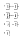
図11に本実施形態の焦電型検出器を含む電子機器の構成例を示す。この電子機器は、光学系400、センサーデバイス(焦電型検出装置)410、画像処理部420、処理部430、記憶部440、操作部450、表示部460を含む。なお本実施形態の電子機器は図11の構成に限定されず、その構成要素の一部(例えば光学系、操作部、表示部等)を省略したり、他の構成要素を追加したりするなどの種々の変形実施が可能である。
4). Electronic Device FIG. 11 shows a configuration example of an electronic device including the pyroelectric detector of the present embodiment. The electronic apparatus includes an
光学系400は、例えば1又は複数のレンズや、これらのレンズを駆動する駆動部などを含む。そしてセンサーデバイス410への物体像の結像などを行う。また必要であればフォーカス調整なども行う。
The
センサーデバイス410は、上述した本実施形態の焦電型検出器200A(200B,200C)を二次元配列させて構成され、複数の行線(ワード線、走査線)と複数の列線(データ線)が設けられる。センサーデバイス410は、二次元配列された検出器に加えて、行選択回路(行ドライバー)と、列線を介して検出器からのデータを読み出す読み出し回路と、A/D変換部等を含むことができる。二次元配列された各検出器からのデータを順次読み出すことで、物体像の撮像処理を行うことができる。
The
画像処理部420は、センサーデバイス410からのデジタルの画像データ(画素データ)に基づいて、画像補正処理などの各種の画像処理を行う。
The
処理部430は、電子機器の全体の制御を行ったり、電子機器内の各ブロックの制御を行ったりする。この処理部430は、例えばCPU等により実現される。記憶部440は、各種の情報を記憶するものであり、例えば処理部430や画像処理部420のワーク領域として機能する。操作部450は、ユーザーが電子機器を操作するためのインターフェースとなるものであり、例えば各種ボタンやGUI(Graphical User Interface)画面などにより実現される。表示部460は、例えばセンサーデバイス410により取得された画像やGUI画面などを表示するものであり、液晶ディスプレイや有機ELディスプレイなどの各種のディスプレイにより実現される。
The
このように、1セル分の焦電型検出器をセンサーとして用いる他、1セル分の焦電型検出器を二軸方向例えば直交二軸方向に二次元配置することでセンサーデバイス410を構成することができ、こうすると電磁波に起因する熱分布画像を提供することができる。このセンサーデバイス410を用いて、特定物質探知装置、偽造紙幣の判定、封筒内の薬品検出、建造物の非破壊検査などのテラヘルツカメラを用いる電子機器を構成することができる。
As described above, the
図12(A)に図11のセンサーデバイス410の構成例を示す。このセンサーデバイスは、センサーアレイ500と、行選択回路(行ドライバー)510と、読み出し回路520を含む。またA/D変換部530、制御回路550を含むことができる。このセンサーデバイスを用いることで、高性能なテラヘルツカメラを実現できる。
FIG. 12A shows a configuration example of the
センサーアレイ500には、例えば図2に示すように二軸方向に複数のセンサーセルが配列(配置)される。また複数の行線(ワード線、走査線)と複数の列線(データ線)が設けられる。なお行線及び列線の一方の本数が1本であってもよい。例えば行線が1本である場合には、図12(A)において行線に沿った方向(横方向)に複数のセンサーセルが配列される。一方、列線が1本である場合には、列線に沿った方向(縦方向)に複数のセンサーセルが配列される。
In the
図12(B)に示すように、センサーアレイ500の各センサーセルは、各行線と各列線の交差位置に対応する場所に配置(形成)される。例えば図12(B)のセンサーセルは、行線WL1と列線DL1の交差位置に対応する場所に配置されている。他のセンサーセルも同様である。
As shown in FIG. 12B, each sensor cell of the
行選択回路510は、1又は複数の行線に接続される。そして各行線の選択動作を行う。例えば図12(B)のようなQVGA(320×240画素)のセンサーアレイ500(焦点面アレイ)を例にとれば、行線WL0、WL1、WL2・・・・WL239を順次選択(走査)する動作を行う。即ちこれらの行線を選択する信号(ワード選択信号)をセンサーアレイ500に出力する。
The
読み出し回路520は、1又は複数の列線に接続される。そして各列線の読み出し動作を行う。QVGAのセンサーアレイ500を例にとれば、列線DL0、DL1、DL2・・・・DL319からの検出信号(検出電流、検出電荷)を読み出す動作を行う。
The
A/D変換部530は、読み出し回路520において取得された検出電圧(測定電圧、到達電圧)をデジタルデータにA/D変換する処理を行う。そしてA/D変換後のデジタルデータDOUTを出力する。具体的には、A/D変換部530には、複数の列線の各列線に対応して各A/D変換器が設けられる。そして、各A/D変換器は、対応する列線において読み出し回路520により取得された検出電圧のA/D変換処理を行う。なお、複数の列線に対応して1つのA/D変換器を設け、この1つのA/D変換器を用いて、複数の列線の検出電圧を時分割にA/D変換してもよい。
The A /
制御回路550(タイミング生成回路)は、各種の制御信号を生成して、行選択回路510、読み出し回路520、A/D変換部530に出力する。例えば充電や放電(リセット)の制御信号を生成して出力する。或いは、各回路のタイミングを制御する信号を生成して出力する。
The control circuit 550 (timing generation circuit) generates various control signals and outputs them to the
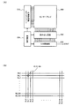
図13に本実施形態の焦電型検出器を含むテラヘルツカメラの例を示す。前述のセンサーデバイス410の電磁波吸収材は、その吸収波長がテラヘルツ波で最適になるように設定されており、テラヘルツ光照射ユニットと組み合わせてテラヘルツカメラ1000を構成した例を示す。
FIG. 13 shows an example of a terahertz camera including the pyroelectric detector of the present embodiment. The electromagnetic wave absorbing material of the above-described
テラヘルツカメラ1000は、制御ユニット1010と、照射光ユニット1020と、光学フィルター1030と、撮像ユニット1040と、表示部1050とを備えて構成されている。撮像ユニット1040は、図示しないレンズなどの光学系と前述の焦電型検出器の電磁波吸収材の吸収波長をテラヘルツ域で最適化したセンサーデバイスを含んで構成されている。
The
制御ユニット1010は、本装置全体を制御するシステムコントローラーを含み、該システムコントローラーは制御ユニットに含まれる光源駆動部および画像処理ユニットを制御する。照射光ユニット1020は、テラヘルツ光(波長が100μm〜1000μmの範囲にある電磁波を指す。)出射するレーザー装置と光学系を含み、テラヘルツ光を検査対象の人物1060に照射する。人物1060からの反射テラヘルツ光は、探知対象である特定物質1070の分光スペクトルのみを通過させる光学フィルター1030を介して撮像ユニット1040に受光される。撮像ユニット1040で生成された画像信号は、制御ユニット1010の画像処理ユニットで所定の画像処理が施され、その画像信号が表示部1050へ出力される。そして人物1060の衣服内等に特定物質1070が存在するか否かにより受光信号の強度が異なるので特定物質1070の存在が判別できる。
The
以上、いくつかの実施形態について説明したが、本発明の新規事項および効果から実体的に逸脱しない多くの変形が可能であることは当業者には容易に理解できるものである。従って、このような変形例はすべて本発明の範囲に含まれるものとする。例えば、明細書又は図面において、少なくとも一度、より広義または同義な異なる用語と共に記載された用語は、明細書又は図面のいかなる箇所においても、その異なる用語に置き換えることができる。 Although several embodiments have been described above, it is easily understood by those skilled in the art that many modifications can be made without substantially departing from the novel matters and effects of the present invention. Accordingly, all such modifications are intended to be included in the scope of the present invention. For example, a term described at least once together with a different term having a broader meaning or the same meaning in the specification or the drawings can be replaced with the different term in any part of the specification or the drawings.
本発明は、種々の焦電型検出器に広く適用することができる。なお、検出する電磁波の波長は、特にテラヘルツ波である場合に有効な技術である。 The present invention can be widely applied to various pyroelectric detectors. Note that the wavelength of the electromagnetic wave to be detected is an effective technique particularly when the wavelength is a terahertz wave.
100 基部(支持部)、102 空洞部、104 支持部(ポスト)、130,140 エッチングストップ膜、150 第1犠牲層、160 反射体、162 コア部材、164 反射膜、200 焦電型検出器、210 支持部材、211A 第1面、211B 第2面、220 検出素子、222,224 第1,第2電極配線層、226,228 第1,第2プラグ、230 キャパシター、232 焦電体、234 第1電極、236 第2電極、240 第1還元ガスバリア層、250 層間絶縁膜(保護膜)、260 第2還元ガスバリア層、270 電磁波吸収体、280 第2犠牲層、290 エッチングストップ膜(支持層、反射膜)、292 エッチングストップ膜、300 第3犠牲層、302 マスク、304 マスク孔、310 反射膜(金属層)、1000 テラヘルツカメラ、1020 照射光ユニット、1040 撮像ユニット。 100 base (support), 102 cavity, 104 support (post), 130, 140 etching stop film, 150 first sacrificial layer, 160 reflector, 162 core member, 164 reflection film, 200 pyroelectric detector, 210 Support member, 211A 1st surface, 211B 2nd surface, 220 detection element, 222,224 1st, 2nd electrode wiring layer, 226,228 1st, 2nd plug, 230 capacitor, 232 pyroelectric body, 234 1st 1 electrode, 236 2nd electrode, 240 1st reducing gas barrier layer, 250 interlayer insulating film (protective film), 260 2nd reducing gas barrier layer, 270 electromagnetic wave absorber, 280 2nd sacrificial layer, 290 etching stop film (support layer, Reflective film), 292 etching stop film, 300 third sacrificial layer, 302 mask, 304 mask hole, 310 Reflection film (metal layer), 1000 terahertz camera, 1020 irradiated light unit, 1040 an imaging unit.
Claims (7)
前記焦電型検出素子の頂部を覆い、かつ、前記焦電型検出素子の頂部より外側に張り出して平板状に形成され、平面視にて前記キャパシターの面積よりも広い面積を有する電磁波吸収体と、
第1面と、前記第1面に対向する第2面とを含み、前記第2面が空洞部に臨んで配置され、前記第1面が前記第1電極と接して前記焦電型検出素子を搭載する支持部材と、
前記支持部材の前記第2面の一部を支持する支持部と、
前記焦電型検出素子の周囲に配置され、入射された電磁波を前記電磁波吸収体に向けて反射させる反射体と、を有することを特徴とするテラヘルツカメラ。 A pyroelectric detection element including a first electrode, a second electrode, and a pyroelectric material disposed between the first and second electrodes, and including a capacitor whose polarization amount changes based on temperature;
An electromagnetic wave absorber that covers a top portion of the pyroelectric detection element and is formed in a flat plate shape and projects outward from the top portion of the pyroelectric detection element, and has an area larger than the area of the capacitor in plan view; ,
The pyroelectric detection element includes a first surface and a second surface facing the first surface, the second surface facing the cavity, and the first surface is in contact with the first electrode A support member for mounting
A support part for supporting a part of the second surface of the support member;
A terahertz camera comprising: a reflector disposed around the pyroelectric detection element and reflecting an incident electromagnetic wave toward the electromagnetic wave absorber.
前記支持部材は、前記焦電型検出素子が搭載される搭載部と、前記搭載部と前記支持部とを連結するアーム部と、を含み、
前記支持部は、前記搭載部の周囲に配置される隔壁部を含み、
前記反射体は、前記隔壁部上に配置されることを特徴とするテラヘルツカメラ。 In claim 1,
The support member includes a mounting portion on which the pyroelectric detection element is mounted, and an arm portion that connects the mounting portion and the support portion,
The support part includes a partition part disposed around the mounting part,
The terahertz camera, wherein the reflector is disposed on the partition wall.
前記反射体は、斜面を有するコア部材と、前記コア部材に被覆される反射層と、を含むことを特徴とするテラヘルツカメラ。 In claim 1 or 2,
The terahertz camera, wherein the reflector includes a core member having a slope and a reflective layer covered with the core member.
前記隔壁部は平面視で矩形リング状に形成され、前記少なくとも一軸方向にて隣り合う2つのセルは、前記2つのセルの間に位置する前記隔壁の一辺が共有され、
前記隔壁の一辺上に形成される前記反射体は、前記隔壁側を底辺とする縦断面が三角形状に形成され、前記2つのセルの間に入射された電磁波を、前記2つのセルの各々の前記電磁波吸収体に向けて反射させることを特徴とするテラヘルツカメラ。 The terahertz camera according to claim 2 is a cell, and a pyroelectric detection device in which a plurality of cells are arranged along at least one axis direction,
The partition wall is formed in a rectangular ring shape in plan view, and the two cells adjacent in at least one axial direction share one side of the partition located between the two cells,
The reflector formed on one side of the partition wall has a triangular cross section with the partition wall side as a base, and electromagnetic waves incident between the two cells are transmitted to each of the two cells. A terahertz camera, which is reflected toward the electromagnetic wave absorber.
Priority Applications (1)
| Application Number | Priority Date | Filing Date | Title |
|---|---|---|---|
| JP2012008714A JP2013148444A (en) | 2012-01-19 | 2012-01-19 | Terahertz camera and electronic apparatus |
Applications Claiming Priority (1)
| Application Number | Priority Date | Filing Date | Title |
|---|---|---|---|
| JP2012008714A JP2013148444A (en) | 2012-01-19 | 2012-01-19 | Terahertz camera and electronic apparatus |
Publications (1)
| Publication Number | Publication Date |
|---|---|
| JP2013148444A true JP2013148444A (en) | 2013-08-01 |
Family
ID=49046066
Family Applications (1)
| Application Number | Title | Priority Date | Filing Date |
|---|---|---|---|
| JP2012008714A Pending JP2013148444A (en) | 2012-01-19 | 2012-01-19 | Terahertz camera and electronic apparatus |
Country Status (1)
| Country | Link |
|---|---|
| JP (1) | JP2013148444A (en) |
-
2012
- 2012-01-19 JP JP2012008714A patent/JP2013148444A/en active Pending
Similar Documents
| Publication | Publication Date | Title |
|---|---|---|
| JP5636787B2 (en) | Thermal photodetector, thermal photodetector, and electronic device | |
| US8648304B1 (en) | Thermal detector, thermal detection device, electronic instrument, and thermal detector manufacturing method | |
| US9000372B2 (en) | Thermal detector, thermal detection device and electronic instrument, and method for manufacturing thermal detector | |
| US8643133B2 (en) | Thermal detector, thermal detection device, and electronic instrument | |
| JP5218460B2 (en) | Pyroelectric detector, pyroelectric detector and electronic device | |
| JP5521827B2 (en) | Pyroelectric detector, pyroelectric detector and electronic device | |
| JP2012026861A (en) | Thermal type detector, thermal type detection device and electronic equipment | |
| JP5585241B2 (en) | Pyroelectric detector, pyroelectric detector and electronic device | |
| JP5589486B2 (en) | Pyroelectric detector, pyroelectric detector and electronic device | |
| JP5589605B2 (en) | Pyroelectric detector, pyroelectric detector and electronic device | |
| JP2012037407A (en) | Pyroelectric type detector, pyroelectric type detecting device and electronic apparatus | |
| JP2015198155A (en) | Thermoelectric conversion element, photo-detection device and electronic device | |
| JP2013148444A (en) | Terahertz camera and electronic apparatus | |
| JP2015135264A (en) | Pyroelectric detector, pyroelectric detector, electronic equipment | |
| JP2013160708A (en) | Pyroelectric detector, pyroelectric detection device and electronic apparatus | |
| JP5915716B2 (en) | Thermal photodetector, thermal photodetector, and electronic device | |
| JP2013148492A (en) | Terahertz camera and electronic apparatus | |
| JP2012154685A (en) | Thermal photodetector, thermal photodetection device, electronic instrument, and method of manufacturing thermal photodetector | |
| JP2012026860A (en) | Pyroelectric photodetector and electronic equipment | |
| JP2013134079A (en) | Terahertz camera and electronic apparatus | |
| JP5846265B2 (en) | Pyroelectric detector, pyroelectric detector and electronic device | |
| JP2015169495A (en) | Thermal photodetector, thermal photodetector, and electronic device | |
| JP2015161642A (en) | Pyroelectric detector, pyroelectric detector, electronic equipment | |
| JP5240373B2 (en) | Pyroelectric detector, pyroelectric detector, and electronic device | |
| JP2013134081A (en) | Terahertz camera and electronic apparatus |