JP2013147708A - METHOD FOR DEPOSITING TiSiN FILM AND STORAGE MEDIUM - Google Patents
METHOD FOR DEPOSITING TiSiN FILM AND STORAGE MEDIUM Download PDFInfo
- Publication number
- JP2013147708A JP2013147708A JP2012009613A JP2012009613A JP2013147708A JP 2013147708 A JP2013147708 A JP 2013147708A JP 2012009613 A JP2012009613 A JP 2012009613A JP 2012009613 A JP2012009613 A JP 2012009613A JP 2013147708 A JP2013147708 A JP 2013147708A
- Authority
- JP
- Japan
- Prior art keywords
- gas
- film
- tisin
- supplying
- forming
- Prior art date
- Legal status (The legal status is an assumption and is not a legal conclusion. Google has not performed a legal analysis and makes no representation as to the accuracy of the status listed.)
- Pending
Links
Images




Landscapes
- Chemical Vapour Deposition (AREA)
- Electrodes Of Semiconductors (AREA)
Abstract
【課題】膜厚にかかわらず安定した比抵抗のTiSiN膜を成膜すること。
【解決手段】被処理基板を処理容器内に搬入し、処理容器内を減圧状態に保持し、被処理基板を加熱しつつ、被処理基板のSiを含む部分の上に、(1)Ti含有ガスを供給するステップまたはTi含有ガスおよび窒化ガスを供給するステップ、(2)窒化ガスを供給するステップ、および(3)Clを含むSi含有ガスを供給するステップの(1)〜(3)を含む、被処理基板上にTiSiN単位膜を形成する操作を複数回行って所定膜厚のTiSiN膜を成膜する際に、成膜の最初にTi含有ガスおよび窒化ガスを供給するステップを行うか、またはTi含有ガスを供給するステップおよび窒化ガスを供給するステップを行って、TiN膜を連続膜の状態で形成する。
【選択図】図3A TiSiN film having a stable specific resistance regardless of the film thickness is formed.
A substrate to be processed is carried into a processing container, the inside of the processing container is held in a reduced pressure state, and the substrate to be processed is heated on a portion containing Si of the substrate to be processed. (1) to (3) of supplying a gas or supplying a Ti-containing gas and a nitriding gas, (2) supplying a nitriding gas, and (3) supplying a Si-containing gas containing Cl. Whether to perform a step of supplying a Ti-containing gas and a nitriding gas at the beginning of film formation when forming a TiSiN unit film on a substrate to be processed a plurality of times to form a TiSiN film having a predetermined thickness Alternatively, a TiN film is formed in a continuous film state by performing a step of supplying a Ti-containing gas and a step of supplying a nitriding gas.
[Selection] Figure 3
Description
本発明は、TiSiN膜の成膜方法および記憶媒体に関する。 The present invention relates to a method for forming a TiSiN film and a storage medium.
DRAMキャパシタの下部電極として、従来からTiN膜が用いられている。TiN膜の成膜手法としては、微細な回路パターンでも良好なステップカバレッジが得られるCVD(Chemical Vapor Deposition)が採用されている(例えば特許文献1)。CVDによってTiN膜を成膜する場合には、Ti含有ガスとしてのTiCl4ガスと窒化ガスとしてのNH3ガスが用いられる。また、より低温で成膜する等の目的で、TiN膜の成膜と窒化が交互的に繰り返されるSFD(Sequential Flow Deposition)あるいは、これらガスを交互的に供給するALD(Atomic Layer Deposition)も提案されている(例えば特許文献2)。 Conventionally, a TiN film is used as a lower electrode of a DRAM capacitor. As a method for forming a TiN film, CVD (Chemical Vapor Deposition) that can provide good step coverage even with a fine circuit pattern is employed (for example, Patent Document 1). When a TiN film is formed by CVD, TiCl 4 gas as a Ti-containing gas and NH 3 gas as a nitriding gas are used. In addition, SFD (Sequential Flow Deposition) in which TiN film formation and nitridation are alternately repeated, or ALD (Atomic Layer Deposition) in which these gases are alternately supplied is proposed for the purpose of film formation at a lower temperature. (For example, Patent Document 2).
半導体デバイスの微細化にともない、DRAMキャパシタの下部電極の薄膜化が進んでおり、インテグレーション時における耐薬品性、および耐酸化性が要求されるようになっているが、従来のTiN膜では耐薬品性および耐酸化性の要求に対して十分な性能が得られていない。 With the miniaturization of semiconductor devices, the lower electrode of DRAM capacitors is becoming thinner, and chemical resistance and oxidation resistance during integration are required. However, conventional TiN films are resistant to chemicals. However, sufficient performance is not obtained with respect to the demands for stability and oxidation resistance.
そこで、これら特性を向上させるべく、DRAMキャパシタの下部電極としてTiN膜にSiをドーピングしたTiSiN膜の適用が検討されている。CVDにより、DRAMキャパシタの下部電極等として適用可能なTiSiN膜を成膜する方法は特許文献3に開示されている。また、ALDによるTiSiN膜を成膜する方法が特許文献4に開示されている。さらに、TiN膜と同様、SFDによるTiSiN膜の成膜も検討されている。
In order to improve these characteristics, application of a TiSiN film obtained by doping Si into a TiN film as a lower electrode of a DRAM capacitor has been studied. A method of forming a TiSiN film applicable as a lower electrode of a DRAM capacitor by CVD is disclosed in
しかしながら、SiO2膜のようなSi含有部分にSFDやALDによりTiSiN膜を成膜する場合、膜厚が薄くなるに従って、比抵抗が著しく上昇することがあるという問題点がある。 However, when a TiSiN film is formed on a Si-containing portion such as a SiO 2 film by SFD or ALD, there is a problem that the specific resistance may be significantly increased as the film thickness is reduced.
本発明はかかる事情に鑑みてなされたものであって、膜厚にかかわらず安定した比抵抗のTiSiN膜を得ることができるTiSiN膜の成膜方法を提供することを課題とする。また、そのような方法を実行するためのプログラムを記憶した記憶媒体を提供することを課題とする。 This invention is made | formed in view of this situation, Comprising: It aims at providing the film-forming method of the TiSiN film | membrane which can obtain the TiSiN film | membrane of the stable specific resistance irrespective of film thickness. Another object of the present invention is to provide a storage medium storing a program for executing such a method.
上記課題を解決するため、本発明は、被処理基板を処理容器内に搬入し、前記処理容器内を減圧状態に保持し、被処理基板を加熱しつつ、被処理基板のSiを含む部分の上に、(1)Ti含有ガスを供給するステップまたはTi含有ガスおよび窒化ガスを供給するステップ、(2)窒化ガスを供給するステップ、および(3)Clを含むSi含有ガスを供給するステップの(1)〜(3)を含む、被処理基板上にTiSiN単位膜を形成する操作を複数回行って所定膜厚のTiSiN膜を成膜するTiSiN膜の成膜方法であって、成膜の最初に前記Ti含有ガスおよび窒化ガスを供給するステップを行うか、または前記Ti含有ガスを供給するステップおよび前記窒化ガスを供給するステップを行って、TiN膜を連続膜の状態で形成することを特徴とするTiSiN膜の成膜方法を提供する。 In order to solve the above problems, the present invention carries a substrate to be processed into a processing container, maintains the inside of the processing container in a reduced pressure state, heats the substrate to be processed, and includes a Si-containing portion of the substrate to be processed. (1) supplying a Ti-containing gas or supplying a Ti-containing gas and a nitriding gas; (2) supplying a nitriding gas; and (3) supplying a Si-containing gas containing Cl. A method of forming a TiSiN film, including (1) to (3), wherein a TiSiN unit film is formed on a substrate to be processed a plurality of times to form a TiSiN film having a predetermined thickness. First, the step of supplying the Ti-containing gas and the nitriding gas is performed, or the step of supplying the Ti-containing gas and the step of supplying the nitriding gas are performed to form a TiN film in a continuous film state. It provides a method of forming a TiSiN film characterized by and.
本発明において、前記Ti含有ガスとしてTiCl4ガス、前記窒化ガスとしてNH3ガス、前記Clを含むSi含有ガスとしてSiH2Cl2ガスを好適に用いることができる。また、成膜されるTiSiN膜の厚さが20nm以下であることが好ましい。 In the present invention, TiCl 4 gas as the Ti-containing gas, NH 3 gas as the nitriding gas, and SiH 2 Cl 2 gas as the Si-containing gas containing Cl can be suitably used. The thickness of the TiSiN film to be formed is preferably 20 nm or less.
また、本発明において、最初に前記(1)〜(2)のステップを、前記処理容器内をパージするステップを挟んで順番で実施し、その後に、前記TiSiN単位膜を形成する操作として、前記(1)〜(3)のステップを、前記処理容器内をパージするステップを挟んで任意の順番で実施する操作を、複数回繰り返すようにすることができる。 In the present invention, first, the steps (1) to (2) are sequentially performed with the step of purging the inside of the processing container, and then the TiSiN unit film is formed as an operation. The operation of performing the steps (1) to (3) in an arbitrary order with the step of purging the inside of the processing container may be repeated a plurality of times.
また、前記TiSiN単位膜を形成する操作は、前記Ti含有ガスおよび窒化ガスを供給するステップ、前記窒化ガスを供給するステップ、前記Clを含むSi含有ガスを供給するステップ、および前記窒化ガスを供給するステップを、前記処理容器内をパージするステップを挟んでこの順で行い、成膜初期から前記TiSiN単位膜を形成する操作を繰り返すものとすることができる。この場合に、2回の前記窒化ガスを供給するステップのうちいずれか一方を省略することができる。 The operation of forming the TiSiN unit film includes the steps of supplying the Ti-containing gas and nitriding gas, supplying the nitriding gas, supplying the Si-containing gas containing Cl, and supplying the nitriding gas. This step is performed in this order across the step of purging the inside of the processing container, and the operation of forming the TiSiN unit film can be repeated from the initial stage of film formation. In this case, one of the two steps of supplying the nitriding gas can be omitted.
さらに、前記TiSiN単位膜を形成する操作は、前記Ti含有ガスを供給するステップ、前記窒化ガスを供給するステップ、および前記Clを含むSi含有ガスを供給するステップを、前記処理容器内をパージするステップを挟んでこの順で行い、成膜初期から前記TiSiN単位膜を形成する操作を繰り返すものとすることができる。この場合に、前記Clを含むSi含有ガスを供給するステップの後に、パージガスを挟んで他の窒化ガスを供給するステップを行ってもよい。 Further, in the operation of forming the TiSiN unit film, the inside of the processing vessel is purged with the step of supplying the Ti-containing gas, the step of supplying the nitriding gas, and the step of supplying the Si-containing gas containing Cl. It is possible to repeat the operation of forming the TiSiN unit film from the initial stage of the film formation in this order across the steps. In this case, after supplying the Si-containing gas containing Cl, a step of supplying another nitriding gas with a purge gas interposed may be performed.
本発明はまた、コンピュータ上で動作し、成膜装置を制御するためのプログラムが記憶された記憶媒体であって、前記プログラムは、実行時に、上記成膜方法が行われるように、コンピュータに前記成膜装置を制御させることを特徴とする記憶媒体を提供する。 The present invention is also a storage medium that operates on a computer and stores a program for controlling the film forming apparatus, and the program is stored in the computer so that the film forming method is performed at the time of execution. A storage medium characterized by controlling a film formation apparatus is provided.
本発明によれば、(1)Ti含有ガスを供給するステップまたはTi含有ガスおよび窒化ガスを供給するステップ、(2)窒化ガスを供給するステップ、および(3)Clを含むSi含有ガスを供給するステップの(1)〜(3)を含む、被処理基板のSiを含む部分の上にTiSiN単位膜を形成する操作を複数回繰り返すTiSiN膜の成膜シーケンスにおいて、成膜の最初にTi含有ガスおよび窒化ガスを供給するステップを行うか、またはTi含有ガスを供給するステップおよび窒化ガスを供給するステップを行って、TiN膜を連続膜の状態で形成し、その後Clを含むSi含有ガスを供給するので、下地のSiを含む部分とTiSiN膜との界面にSi−Cl結合を形成することがなく、膜厚が薄い場合にも安定した比抵抗のTiSiN膜を得ることができる。 According to the present invention, (1) supplying Ti-containing gas or supplying Ti-containing gas and nitriding gas, (2) supplying nitriding gas, and (3) supplying Si-containing gas containing Cl. In the TiSiN film formation sequence in which the operation of forming the TiSiN unit film on the Si-containing portion of the substrate to be processed, including the steps (1) to (3) is repeated a plurality of times, Ti is contained at the beginning of film formation. A step of supplying a gas and a nitriding gas is performed, or a step of supplying a Ti-containing gas and a step of supplying a nitriding gas are performed to form a TiN film in a continuous film state, and then a Si-containing gas containing Cl is formed. Therefore, the Si-Cl bond is not formed at the interface between the Si-containing portion of the base and the TiSiN film, and a stable specific resistance T can be obtained even when the film thickness is thin. It can be obtained SiN film.
以下、添付図面を参照して本発明の実施形態について具体的に説明する。
図1は本発明の一実施形態に係るTiSiN膜の成膜方法の実施に用いる成膜装置の一例を示す概略断面図である。ここでは、熱CVDによりTiSiN膜を成膜する場合を例にとって説明する。
Hereinafter, embodiments of the present invention will be specifically described with reference to the accompanying drawings.
FIG. 1 is a schematic cross-sectional view showing an example of a film forming apparatus used for carrying out a method of forming a TiSiN film according to an embodiment of the present invention. Here, a case where a TiSiN film is formed by thermal CVD will be described as an example.
なお、以下の説明において、ガスの流量の単位はmL/minを用いているが、ガスは温度および気圧により体積が大きく変化するため、本発明では標準状態に換算した値を用いている。なお、標準状態に換算した流量は通常sccm(Standerd Cubic Centimeter per Minutes)で標記されるためsccmを併記している。ここにおける標準状態は、温度0℃(273.15K)、気圧1atm(101325Pa)の状態である。 In the following description, the unit of the gas flow rate is mL / min. However, since the volume of the gas greatly changes depending on the temperature and the atmospheric pressure, the value converted into the standard state is used in the present invention. In addition, since the flow volume converted into the standard state is normally indicated by sccm (Standard Cubic Centimeter per Minutes), sccm is also written together. The standard state here is a state where the temperature is 0 ° C. (273.15 K) and the atmospheric pressure is 1 atm (101325 Pa).
この成膜装置100は、略円筒状のチャンバ1を有している。チャンバ1の内部には、被処理基板であるウエハWを水平に支持するためのステージとして、AlNで構成されたサセプタ2がその中央下部に設けられた円筒状の支持部材3により支持された状態で配置されている。サセプタ2の外縁部にはウエハWをガイドするためのガイドリング4が設けられている。また、サセプタ2にはモリブデン等の高融点金属で構成されたヒーター5が埋め込まれており、このヒーター5はヒーター電源6から給電されることにより被処理基板であるウエハWを所定の温度に加熱する。
The
チャンバ1の天壁1aには、シャワーヘッド10が設けられている。このシャワーヘッド10は、上段ブロック体10a、中段ブロック体10b、下段ブロック体10cで構成されており、全体が略円盤状をなしている。上段ブロック体10aは、中段ブロック体10bおよび下段ブロック体10cとともにシャワーヘッド本体部を構成する水平部10dとこの水平部10dの外周上方に連続する環状支持部10eとを有し、凹状に形成されている。そして、この環状支持部10eによりシャワーヘッド10全体が支持されている。そして、下段ブロック体10cにはガスを吐出する吐出孔17と18とが交互に形成されている。上段ブロック体10aの上面には、第1のガス導入口11と、第2のガス導入口12とが形成されている。上段ブロック体10aの中では、第1のガス導入口11から多数のガス通路13が分岐している。中段ブロック体10bにはガス通路15が形成されており、上記ガス通路13が水平に延びる連通路13aを介してこれらガス通路15に連通している。さらにこのガス通路15が下段ブロック体10cの吐出孔17に連通している。また、上段ブロック体10aの中では、第2のガス導入口12から多数のガス通路14が分岐している。中段ブロック体10bにはガス通路16が形成されており、上記ガス通路14がこれらガス通路16に連通している。さらにこのガス通路16が中段ブロック体10b内に水平に延びる連通路16aに接続されており、この連通路16aが下段ブロック体10cの多数の吐出孔18に連通している。そして、上記第1および第2のガス導入口11,12は、ガス供給機構20のガスラインに接続されている。
A
ガス供給機構20は、Ti含有ガスとしてのTiCl4ガスを供給するTiCl4ガス供給源21と、窒化ガスとしてのNH3ガスを供給するNH3ガス供給源23とを有している。TiCl4ガス供給源21にはTiCl4ガス供給ライン22が接続されており、このTiCl4ガス供給ライン22は第1のガス導入口11に接続されている。NH3ガス供給源23にはNH3ガス供給ライン24が接続されており、このNH3ガス供給ライン24は第2のガス導入口12に接続されている。
TiCl4ガス供給ライン22にはN2ガス供給ライン26が接続されており、このN2ガス供給ライン26にはN2ガス供給源25からN2ガスがキャリアガスまたはパージガスとして供給されるようになっている。
TiCl 4 the
NH3ガス供給ライン24にはSi含有ガスとしてのジクロロシラン(SiH2Cl2;DCS)ガスを供給するDCSガス供給ライン28が接続されており、このDCSガス供給ライン28にはDCSガス供給源27からDCSガスが供給されるようになっている。また、NH3ガス供給ライン24にはN2ガス供給ライン30が接続されており、このN2ガス供給ライン30にはN2ガス供給源29からN2ガスがキャリアガスまたはパージガスとして供給されるようになっている。
A DCS
また、ガス供給機構20は、クリーニングガスであるClF3ガスを供給するClF3ガス供給源31を有しており、ClF3ガス供給源31にはClF3ガス供給ライン32aが接続されている。このClF3ガス供給ライン32aは、TiCl4ガス供給ライン22に接続されている。また、ClF3ガス供給ライン32aから分岐して、NH3ガス供給ライン24に接続されるClF3ガス供給ライン32bが設けられている。
The
TiCl4ガス供給ライン22、NH3ガス供給ライン24、DCSガス供給ライン28、N2ガス供給ライン26、30、ClF3ガス供給ライン32aには、マスフローコントローラ33およびマスフローコントローラ33を挟む2つのバルブ34が設けられている。また、ClF3ガス供給ライン32bには、バルブ34が設けられている。
The TiCl 4
したがって、TiCl4ガス供給源21からのTiCl4ガスおよびN2ガス供給源25からのN2ガスは、TiCl4ガス供給ライン22を介してシャワーヘッド10の第1のガス導入口11からシャワーヘッド10内に至り、ガス通路13,15を経て吐出孔17からチャンバ1内へ吐出され、NH3ガス供給源23からのNH3ガス、DCSガス供給源27からのDCSガスおよびN2ガス供給源29からのN2ガスは、NH3ガス供給ライン24を介してシャワーヘッド10の第2のガス導入口12からシャワーヘッド10内に至り、ガス通路14,16を経て吐出孔18からチャンバ1内へ吐出される。すなわち、シャワーヘッド10は、TiCl4ガスとNH3ガスおよびDCSガスとが別個にチャンバ1内に供給されるようになっている。なお、これに限らず全てのガスがシャワーヘッド10内で同じ通路を通ってチャンバ1内に供給されるタイプであってもよい。また、NH3ガスおよびDCSガスがガス供給ラインからシャワーヘッドにかけて同じ通路を通ってチャンバに供給されるようになっているが、さらにもう一段、別個のガス導入口およびシャワーヘッド内ガス通路、吐出口を設けて、シャワーヘッド内部でNH3ガスとDCSガスとが混合されないようにしてもよい。また、DCSガス供給ラインがNH3ガス供給ラインに接続されている例を示したが、DCSガス供給ラインはTiCl4ガス供給ラインに接続されていてもよい。
Therefore, the shower head from the first
なお、Ti含有ガスとしては、TiCl4以外に、テトラ(イソプロポキシ)チタン(TTIP)、四臭化チタン(TiBr4)、四ヨウ化チタン(TiI4)、テトラキスエチルメチルアミノチタン(TEMAT)、テトラキスジメチルアミノチタン(TDMAT)、テトラキスジエチルアミノチタン(TDEAT)等を用いることもできる。また、窒化ガスとしては、NH3以外に、モノメチルヒドラジン(MMH)を用いることもできる。さらに、Si含有ガスとしてはDCS以外に、テトラクロロシラン(SiCl4;STC)、トリクロロシラン(SiHCl3;TCS)、モノクロロシラン(SiH3Cl;MCS)等のClを含有したものを挙げることができる。また、キャリアガスおよびパージガスとして用いるN2ガスの代わりに、Arガス等の他の不活性ガスを用いることもできる。 As Ti-containing gas, in addition to TiCl 4 , tetra (isopropoxy) titanium (TTIP), titanium tetrabromide (TiBr 4 ), titanium tetraiodide (TiI 4 ), tetrakisethylmethylaminotitanium (TEMAT), Tetrakisdimethylaminotitanium (TDMAT), tetrakisdiethylaminotitanium (TDEAT), etc. can also be used. In addition to NH 3 , monomethylhydrazine (MMH) can also be used as the nitriding gas. Further, examples of the Si-containing gas include those containing Cl such as tetrachlorosilane (SiCl 4 ; STC), trichlorosilane (SiHCl 3 ; TCS), and monochlorosilane (SiH 3 Cl; MCS) in addition to DCS. . Further, instead of the N 2 gas used as the carrier gas and the purge gas, other inert gases such as Ar gas can be used.
シャワーヘッド10の上段ブロック体10aの水平部10dには、シャワーヘッド10を加熱するためのヒーター45が設けられている。このヒーター45にはヒーター電源46が接続されており、ヒーター電源46からヒーター45に給電することによりシャワーヘッド10が所望の温度に加熱される。上段ブロック体10aの凹部にはヒーター45による加熱効率を上げるために断熱部材47が設けられている。
A
チャンバ1の底壁1bの中央部には円形の穴35が形成されており、底壁1bにはこの穴35を覆うように下方に向けて突出する排気室36が設けられている。排気室36の側面には排気管37が接続されており、この排気管37には排気装置38が接続されている。そしてこの排気装置38を作動させることによりチャンバ1内を所定の真空度まで減圧することが可能となっている。
A
サセプタ2には、ウエハWを支持して昇降させるための3本(2本のみ図示)のウエハ支持ピン39がサセプタ2の表面に対して突没可能に設けられ、これらウエハ支持ピン39は支持板40に支持されている。そして、ウエハ支持ピン39は、エアシリンダ等の駆動機構41により支持板40を介して昇降される。
The
チャンバ1の側壁には、チャンバ1と隣接して設けられた図示しないウエハ搬送室との間でウエハWの搬入出を行うための搬入出口42と、この搬入出口42を開閉するゲートバルブ43とが設けられている。
On the side wall of the
成膜装置100の構成部であるヒーター電源6および46、バルブ34、マスフローコントローラ33、駆動機構41等は、マイクロプロセッサ(コンピュータ)を備えた制御部50に接続されて制御される構成となっている。また、制御部50には、オペレータが成膜装置100を管理するためにコマンドの入力操作等を行うキーボードや、成膜装置100の稼働状況を可視化して表示するディスプレイ等からなるユーザーインターフェース51が接続されている。さらに、制御部50には、成膜装置100で実行される各種処理を制御部50の制御にて実現するためのプログラムや、処理条件に応じて成膜装置100の各構成部に処理を実行させるためのプログラムすなわち処理レシピが格納された記憶部52が接続されている。処理レシピは記憶部52中の記憶媒体52aに記憶されている。記憶媒体はハードディスク等の固定的なものであってもよいし、CDROM、DVD等の可搬性のものであってもよい。また、他の装置から、例えば専用回線を介して処理レシピを適宜伝送させるようにしてもよい。そして、必要に応じて、ユーザーインターフェース51からの指示等にて任意の処理レシピを記憶部52から呼び出して制御部50に実行させることで、制御部50の制御下で、成膜装置100での所望の処理が行われる。
The
次に、以上のような成膜装置100における本実施形態に係るTiSiN膜の成膜方法について説明する。
Next, a TiSiN film forming method according to the present embodiment in the
まず、チャンバ1内を排気装置38により真空引き状態とし、N2ガス供給源25および29からN2ガスをシャワーヘッド10を介してチャンバ1内に導入しつつ、ヒーター5によりチャンバ1内を、成膜温度に予備加熱し、温度が安定した時点で、TiCl4ガスおよびNH3ガスをシャワーヘッド10を介して所定流量でチャンバ1内に導入し、チャンバ1内壁、排気室36内壁およびシャワーヘッド10等のチャンバ内部材表面にTiN膜をプリコートする。この際、TiCl4ガス、NH3ガスおよびDCSガスを導入してチャンバ内部材表面にTiSiN膜をプリコートしてもよいし、TiN膜とTiSiN膜との積層膜をプリコートしてもよい。
First, the vacuum state in the
プリコート処理が終了後、ゲートバルブ43を開にして、ウエハ搬送室から搬送装置により(いずれも図示せず)搬入出口42を介してウエハWをチャンバ1内へ搬入し、サセプタ2に載置する。そして、ヒーター5によりウエハWを300〜900℃に加熱し、チャンバ1内にN2ガスを供給してウエハWの予備加熱を行う。ウエハの温度がほぼ安定した時点で、TiSiN膜の成膜を開始する。
After the pre-coating process is completed, the
本実施形態に係るTiSiN膜の成膜方法においては、Ti含有ガス、窒化ガス、Si含有ガスを用いてSFDまたはALDの手法によりTiSiN膜を成膜する。Si含有ガスとしては、DCSに代表されるClを含むものを用いる。 In the TiSiN film forming method according to the present embodiment, the TiSiN film is formed by SFD or ALD using a Ti-containing gas, a nitriding gas, and a Si-containing gas. A gas containing Cl typified by DCS is used as the Si-containing gas.
すなわち、(1)Ti含有ガスを供給するステップまたはTi含有ガスおよび窒化ガスを供給するステップ、(2)窒化ガスを供給するステップ、(3)Clを含むSi含有ガスを供給するステップの(1)〜(3)のステップをパージガスの供給を挟んで適宜の順序で行う操作によりTiSiN単位膜を形成し、このTiSiN単位膜を形成する操作を複数回繰り返して所定の膜厚のTiSiN膜を成膜する。一回のTiSiN単位膜を形成する操作において、上記(1)〜(3)のステップは、一回に限らない。特に(2)の窒化ステップは、(1)のステップの後および(3)のステップの後の両方に行うと、より窒化が促進されるので好ましい。 That is, (1) supplying Ti-containing gas or supplying Ti-containing gas and nitriding gas, (2) supplying nitriding gas, and (3) supplying Si-containing gas containing Cl (1) The TiSiN unit film is formed by performing the steps (3) to (3) in an appropriate order with the purge gas supplied, and this TiSiN unit film is formed a plurality of times to form a TiSiN film having a predetermined thickness. Film. In the operation of forming the TiSiN unit film once, the steps (1) to (3) are not limited to once. In particular, the nitriding step (2) is preferably performed both after the step (1) and after the step (3) because nitriding is further promoted.
次に、具体的なシーケンスについて、図2のタイミングチャートを参照して説明する。
本シーケンスでは、図1の成膜装置に示すように、Ti含有ガスとしてTiCl4ガス、窒化ガスとしてNH3ガス、Si含有ガスとしてDCSガス、パージガスとしてN2ガスを用いる。最初に、N2ガス供給源25,29からN2ガスをキャリアガスとして流し、TiCl4ガス供給源21およびNH3ガス供給源23からTiCl4ガスおよびNH3ガスをチャンバ1内に短時間供給し、分子層レベルの薄いTiN膜をウエハW上に堆積させる(TiN成膜)(ステップS1)。次いで、TiCl4ガスおよびNH3ガスの供給を停止し、N2ガス供給源25,29から流しているN2ガスによりチャンバ1内をパージする(ステップS2)。その後、キャリアガスとしてのN2ガスとともにNH3ガスを供給し、第1の窒化処理を行う(ステップS3)。その後、NH3ガスの供給を停止し、N2ガス供給源25,29から流しているN2ガスによりチャンバ1内をパージする(ステップS4)。その後、キャリアガスとしてのN2ガスとともにDCSガス供給源27からDCSガスを供給し、ウエハW上の薄いTiN膜にSiをドープ(Si成膜)して薄いTiSiN膜を形成する(ステップS5)。その後、DCSガスの供給を停止し、N2ガス供給源25,29から流しているN2ガスによりチャンバ1内をパージする(ステップS6)。その後、キャリアガスとしてのN2ガスとともにNH3ガスを供給し、第2の窒化処理を行う(ステップS7)。その後、NH3ガスの供給を停止し、N2ガス供給源25,29から流しているN2ガスによりチャンバ1内をパージする(ステップS8)。
Next, a specific sequence will be described with reference to the timing chart of FIG.
In this sequence, as shown in the film forming apparatus of FIG. 1, TiCl 4 gas is used as the Ti-containing gas, NH 3 gas is used as the nitriding gas, DCS gas is used as the Si-containing gas, and N 2 gas is used as the purge gas. First, flushed with N 2 gas from the N 2
以上のステップS1〜S8の操作によりTiSiN単位膜が形成され、この操作を1サイクルとして所定回数繰り返し、所定厚さのTiSiN膜を成膜する。このときのサイクル数は、膜厚に応じて適宜設定される。例えば2〜60回程度である。このときのガスの切替は、制御部50からの指令によりバルブを切り替えることにより行われる。
A TiSiN unit film is formed by the operations in steps S1 to S8 described above, and this operation is repeated a predetermined number of times to form a TiSiN film having a predetermined thickness. The number of cycles at this time is appropriately set according to the film thickness. For example, about 2 to 60 times. The gas switching at this time is performed by switching the valve according to a command from the
ところで、SiO2膜のようなSi含有部分にSFDによりTiSiN膜を成膜する場合に、膜厚が薄くなるに従って比抵抗が著しく上昇していく現象が生じる場合があることが判明した。このような現象は、ステップS1の時間が2sec程度の場合に生じるため、成膜初期のインキュベーションタイムと呼ばれる膜が形成されない時間帯が存在することに起因すると考え、以下のような実験を行った。 By the way, it has been found that when a TiSiN film is formed by SFD on a Si-containing portion such as a SiO 2 film, a phenomenon may occur in which the specific resistance increases remarkably as the film thickness decreases. Since such a phenomenon occurs when the time of step S1 is about 2 seconds, the following experiment was conducted on the assumption that there is a time zone during which no film is formed, which is called an incubation time at the initial stage of film formation. .
ここでは、上記シーケンスにより基本条件を以下のように設定し、1回目のステップS1について2回目以降と同じ2secで行ったもの(付加時間なし)と、1回目のステップS1のみ6.7sec長くしたもの(付加時間6.7sec)について、繰り返し回数を変化させ、種々の膜厚のTiSiN膜を成膜し、膜の比抵抗を測定した。 Here, the basic conditions are set as follows by the above sequence, and the first step S1 is performed in 2 sec, the same as the second and subsequent times (no additional time), and only the first step S1 is increased by 6.7 sec. For the sample (addition time 6.7 sec), the number of repetitions was changed, TiSiN films having various thicknesses were formed, and the specific resistance of the films was measured.
・ステップS1(TiN成膜)
チャンバ圧力:260Pa
TiCl4ガス流量:60mL/min(sccm)
NH3ガス流量:60mL/min(sccm)
N2ガス流量(2系統):各170mL/min(sccm)
時間:2sec
・ステップS3(第1の窒化)
チャンバ圧力:260Pa
NH3ガス流量:4500mL/min(sccm)
N2ガス流量(2系統):各200mL/min(sccm)
時間:5sec
・ステップS5(Si成膜)
チャンバ圧力:667Pa
DCSガス流量:25mL/min(sccm)
N2ガス流量(2系統):各500mL/min(sccm)
時間:8sec
・ステップS7(第2の窒化)
チャンバ圧力:260Pa
NH3ガス流量:4500mL/min(sccm)
N2ガス流量(2系統):各200mL/min(sccm)
時間:30sec
・ステップS2、S4、S6、S8(パージ)
N2パージ
・繰り返し数:4〜40回
・サセプタ温度:680℃(ウエハ温度:617℃に相当)
Step S1 (TiN film formation)
Chamber pressure: 260Pa
TiCl 4 gas flow rate: 60 mL / min (sccm)
NH 3 gas flow rate: 60 mL / min (sccm)
N 2 gas flow rate (2 systems): 170 mL / min (sccm) each
Time: 2sec
Step S3 (first nitriding)
Chamber pressure: 260Pa
NH 3 gas flow rate: 4500 mL / min (sccm)
N 2 gas flow rate (2 systems): 200 mL / min (sccm) each
Time: 5 sec
Step S5 (Si film formation)
Chamber pressure: 667Pa
DCS gas flow rate: 25 mL / min (sccm)
N 2 gas flow rate (2 systems): 500 mL / min (sccm) each
Time: 8 sec
Step S7 (second nitriding)
Chamber pressure: 260Pa
NH 3 gas flow rate: 4500 mL / min (sccm)
N 2 gas flow rate (2 systems): 200 mL / min (sccm) each
Time: 30sec
・ Steps S2, S4, S6, S8 (Purge)
N 2 purge • Number of repetitions: 4 to 40 times • Susceptor temperature: 680 ° C. (corresponding to wafer temperature: 617 ° C.)
図3は、上記条件でTiSiN膜を成膜した際における、膜状態のイメージを示す図であり、(a)は1回目のステップS1を2回目以降と同じ2secにした場合(付加時間なし)、(b)は1回目のステップS1のみ6.7sec長くした場合(付加時間6.7sec)である。この図に示すように、(a)の付加時間なしの場合には、TiNのインキュベーション時間よりも短いため、1回目のステップS1およびS2では例えばSiO2膜やSiN膜のような下地絶縁膜上に島状のTiN膜しか成膜されず、部分的に下地絶縁膜が露出した状態となっている。これに対して(b)の付加時間6.7secの場合には、1回目のステップS1およびS2でしっかりしたTiN膜が形成される。 FIG. 3 is a diagram showing an image of a film state when a TiSiN film is formed under the above conditions. FIG. 3A shows a case where the first step S1 is set to 2 sec after the second time (no additional time). (B) shows a case where only the first step S1 is increased by 6.7 sec (addition time 6.7 sec). As shown in this figure, when there is no additional time of (a), it is shorter than the incubation time of TiN, so in the first steps S1 and S2, the base insulating film such as a SiO 2 film or a SiN film is formed. Only the island-like TiN film is formed, and the base insulating film is partially exposed. On the other hand, when the additional time of (b) is 6.7 sec, a firm TiN film is formed in the first steps S1 and S2.
これらシーケンスによりTiSiN膜を成膜した際の膜の走査型顕微鏡(SEM)による膜厚と比抵抗との関係を図4に示す。この図に示すように、(a)の1回目のステップS1が付加時間なしで、初期のTiN膜が十分に成膜されていない場合には、20nm以下の膜厚の領域において、膜厚が薄くなるに従って比抵抗が上昇していることがわかる。現状、DRAMのキャパシタ下部電極に用いられているTiN膜の膜厚は20nm以下のレベルであり、世代が進むにつれて10nm、5nmと薄膜化されていくことが予想されている。そのため、この膜厚領域での比抵抗の変化は、実際のデバイス生産時の膜厚バラツキによる下部電極材料の抵抗値のバラツキが発生することを意味しており、抵抗値のバラツキは信号の伝達速度のばらつきに繋がるため問題である。これに対して、(b)の1回目のステップS1が付加時間6.7secの場合には、膜厚によって比抵抗がほとんど変化していない。 FIG. 4 shows the relationship between the film thickness and specific resistance of the film obtained by forming a TiSiN film by these sequences using a scanning microscope (SEM). As shown in this figure, when the first step S1 of (a) has no additional time and the initial TiN film is not sufficiently formed, the film thickness is 20 nm or less in the region of 20 nm or less. It can be seen that the specific resistance increases as the thickness decreases. At present, the thickness of the TiN film used for the capacitor lower electrode of the DRAM is at a level of 20 nm or less, and it is expected that the film thickness will be reduced to 10 nm and 5 nm as the generation progresses. For this reason, the change in specific resistance in this film thickness region means that the resistance value of the lower electrode material varies due to the film thickness variation during actual device production. This is a problem because it leads to variations in speed. On the other hand, when the first step S1 in (b) has an additional time of 6.7 sec, the specific resistance hardly changes depending on the film thickness.
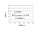
このような違いは、(a)の1回目のステップS1が付加時間なしの場合は、SiO2膜のような下地絶縁膜が露出した状態でDCSガスを供給することになるため、DCSガスはTiやN元素だけでなく、SiやO元素とも触れることとなるのに対し、(b)の1回目のステップS1が付加時間6.7secの場合には、成膜初期に下地絶縁膜上にTiN膜が形成されるのに十分な時間、TiCl4ガスとNH3ガスを流すので、下地絶縁膜のSiO2膜にTiN膜が形成された状態でSiを添加するためのDCSガスを流し始めることとなり、DCSガスはSiやOなどの元素に触れることなくTiN膜に供給されることによる。 Such a difference is that when the first step S1 in (a) has no additional time, the DCS gas is supplied with the underlying insulating film such as the SiO 2 film exposed. When not only Ti and N elements but also Si and O elements are touched, if the first step S1 of (b) is for an additional time of 6.7 sec, it is formed on the underlying insulating film at the initial stage of film formation. Since the TiCl 4 gas and the NH 3 gas are allowed to flow for a sufficient time to form the TiN film, the DCS gas for adding Si is started to flow while the TiN film is formed on the SiO 2 film of the base insulating film. This is because the DCS gas is supplied to the TiN film without touching elements such as Si and O.
この点についてさらに検討する。
上記2つのシーケンスで成膜したTiSiN膜の膜厚(SEM膜厚)による膜中のSi濃度を比較した結果を図5に示す。この図に示すように、両者で膜中のSi濃度は変化しておらず、TiSiN膜へのSiの取り込まれ方は変化していないことがわかる。
This point will be further examined.
FIG. 5 shows the result of comparing the Si concentration in the film according to the film thickness (SEM film thickness) of the TiSiN film formed by the above two sequences. As shown in this figure, it can be seen that the Si concentration in the film is not changed in both cases, and the way of incorporation of Si into the TiSiN film is not changed.
この結果を踏まえると、Si含有ガスとして用いているDCSガスはSiにClが含まれており、TiSiN膜へのSiの取り込まれ方は同じであるから、TiSiN膜へのClの取り込まれ方の違いが、比抵抗の膜厚依存性が変化する原因であると考えられる。 Based on this result, since the DCS gas used as the Si-containing gas contains Cl in Si, and the way in which Si is taken into the TiSiN film is the same, the way in which Cl is taken into the TiSiN film The difference is considered to be the cause of the change in film thickness dependence of specific resistance.
量子化学計算から求めた、表面からCl原子が離脱する場合の乖離エネルギーは、Ti−Cl結合の場合は0.08〜0.29eVであるのに対し、Si−Cl結合の場合は0.54〜0.59eVであり、Si−Cl結合が切れるエネルギーのほうがTi−Cl結合が切れるエネルギーよりも約2〜7倍も高いことがわかる。 The dissociation energy obtained from the quantum chemical calculation when Cl atoms are detached from the surface is 0.08 to 0.29 eV in the case of Ti—Cl bond, whereas 0.54 in the case of Si—Cl bond. It can be seen that the energy at which the Si—Cl bond is broken is about 2 to 7 times higher than the energy at which the Ti—Cl bond is broken.
このことから、成膜初期にClを含むSi含有ガスであるDCSガスを流した時の下地の表面状態が重要であり、下地絶縁膜が露出していると、SiO2やSiNなどを構成している表面のSi元素にDCSに含まれるClやDCSから乖離したCl元素が到達することでSi−Cl結合が形成されると考えられる。下地膜とTiSiN膜の界面付近に、一旦Si−Cl結合が形成されてしまうと、Si−Cl結合の乖離エネルギーが大きいため、通常の成膜過程ではこのSi−Cl結合を切ることは困難であり、その後に引き続くTiN膜の成膜やSiの添加などによって、その上に膜が形成されると、Si−Cl結合はそのまま下地膜とTiSiN膜の界面付近に残ることになると推測される。これに対して、最初にTiN膜を連続膜として形成してやることにより、その表面にCl元素が到達しても、Ti−Cl結合ができることとになり、上述したようにTi−Cl結合は非常に切れやすいので、それがそのまま膜中に残ることはほとんど生じない。 For this reason, the surface state of the base when the DCS gas, which is a Si-containing gas containing Cl, is flowed at the initial stage of film formation is important. When the base insulating film is exposed, SiO 2 , SiN, etc. are formed. It is considered that a Si—Cl bond is formed when Cl contained in DCS or Cl element separated from DCS reaches Si element on the surface. Once the Si-Cl bond is formed near the interface between the base film and the TiSiN film, the energy of the Si-Cl bond is large, so it is difficult to break the Si-Cl bond in the normal film formation process. In addition, when a film is formed thereon by subsequent formation of a TiN film or addition of Si, it is presumed that the Si—Cl bond remains as it is near the interface between the base film and the TiSiN film. On the other hand, by forming the TiN film as a continuous film first, even if the Cl element reaches the surface, Ti—Cl bond can be formed. As described above, the Ti—Cl bond is very high. Since it is easy to cut, it hardly occurs in the film as it is.
このことから、本実施形態では、最初にTiN膜を連続膜の状態で形成してから、Clを含むSi含有ガスであるDCSガスを供給するTiSiN単位膜を形成する操作を複数回繰り返すシーケンスを用いる。これにより比抵抗が膜厚に依存せずほぼ一定なTiSiN膜を形成することができる。 Therefore, in this embodiment, a sequence in which a TiN film is formed in a continuous film state first and then a TiSiN unit film for supplying a DCS gas that is a Si-containing gas containing Cl is repeated a plurality of times. Use. As a result, a TiSiN film whose specific resistance does not depend on the film thickness can be formed.
また、TiSiN単位膜を形成する操作に先立って、少なくともTiN膜を形成するためのインキュベーション時間に相当する時間の間、Ti含有ガスおよび窒化ガスを供給するステップを行うか、またはTi含有ガスを供給するステップおよび窒化ガスを供給するステップを行って、引き続きすぐにTiN膜が形成される状態にしておけば、その後のTiSiN単位膜を形成する操作においては、(1)Ti含有ガスを供給するステップまたはTi含有ガスおよび窒化ガスを供給するステップ、(2)窒化ガスを供給するステップ、および(3)Clを含むSi含有ガスを供給するステップをパージ工程を挟んで任意の順番で実施することができる。この場合にも同様に、比抵抗が膜厚に依存せずほぼ一定なTiSiN膜を形成することができる。 Further, prior to the operation of forming the TiSiN unit film, a step of supplying a Ti-containing gas and a nitriding gas is performed for at least a time corresponding to an incubation time for forming the TiN film, or a Ti-containing gas is supplied. If the TiN film is formed immediately after the step of supplying and the step of supplying the nitriding gas, in the subsequent operation of forming the TiSiN unit film, (1) the step of supplying the Ti-containing gas Alternatively, the step of supplying the Ti-containing gas and the nitriding gas, (2) the step of supplying the nitriding gas, and (3) the step of supplying the Si-containing gas containing Cl may be performed in any order with the purge step interposed therebetween. it can. In this case as well, a TiSiN film whose specific resistance does not depend on the film thickness can be formed.
なお、好ましい条件は、以下の通りである。
・ステップS1
チャンバ内圧力:66.6〜1333Pa、より好ましくは133〜800Pa
TiCl4ガス流量:10〜200mL/min(sccm)、より好ましくは40〜100mL/min(sccm)
NH3ガス流量:10〜200mL/min(sccm)、より好ましくは40〜100mL/min(sccm)
N2ガス流量:100〜10000mL/min(sccm)、より好ましくは300〜4000mL/min(sccm)
時間T1:0.1〜30sec、より好ましくは0.5〜10sec
・ステップS3、S7
チャンバ内圧力:66.6〜1333Pa、より好ましくは133〜800Pa
NH3ガス流量:100〜10000mL/min(sccm)、より好ましくは1000〜5000mL/min(sccm)
N2ガス流量:100〜10000mL/min(sccm)、より好ましくは300〜4000mL/min(sccm)
時間T3、T7:1〜180sec、より好ましくは3〜60sec
・ステップS5
チャンバ内圧力:66.6〜1333Pa、より好ましくは133〜800Pa
DCSガス流量:1〜1000mL/min(sccm)、より好ましくは3〜200mL/min(sccm)
N2ガス流量:100〜10000mL/min(sccm)、より好ましくは300〜4000mL/min(sccm)
時間T5:0.1〜60sec、より好ましくは1〜20sec
・ステップS2、S4、S6、S8(パージ)
N2ガス流量:100〜10000mL/min(sccm)、より好ましくは300〜4000mL/min(sccm)
時間T2、T4、T6、T8:1〜60sec、より好ましくは3〜20sec
・温度(サセプタ温度):400〜700℃
Preferred conditions are as follows.
・ Step S1
Chamber pressure: 66.6 to 1333 Pa, more preferably 133 to 800 Pa
TiCl 4 gas flow rate: 10 to 200 mL / min (sccm), more preferably 40 to 100 mL / min (sccm)
NH 3 gas flow rate: 10 to 200 mL / min (sccm), more preferably 40 to 100 mL / min (sccm)
N 2 gas flow rate: 100 to 10000 mL / min (sccm), more preferably 300 to 4000 mL / min (sccm)
Time T1: 0.1-30 sec, more preferably 0.5-10 sec
・ Steps S3 and S7
Chamber pressure: 66.6 to 1333 Pa, more preferably 133 to 800 Pa
NH 3 gas flow rate: 100-10000 mL / min (sccm), more preferably 1000-5000 mL / min (sccm)
N 2 gas flow rate: 100 to 10000 mL / min (sccm), more preferably 300 to 4000 mL / min (sccm)
Time T3, T7: 1-180 sec, more preferably 3-60 sec
・ Step S5
Chamber pressure: 66.6 to 1333 Pa, more preferably 133 to 800 Pa
DCS gas flow rate: 1-1000 mL / min (sccm), more preferably 3-200 mL / min (sccm)
N 2 gas flow rate: 100 to 10000 mL / min (sccm), more preferably 300 to 4000 mL / min (sccm)
Time T5: 0.1 to 60 sec, more preferably 1 to 20 sec
・ Steps S2, S4, S6, S8 (Purge)
N 2 gas flow rate: 100 to 10000 mL / min (sccm), more preferably 300 to 4000 mL / min (sccm)
Time T2, T4, T6, T8: 1 to 60 sec, more preferably 3 to 20 sec
-Temperature (susceptor temperature): 400-700 ° C
図2のシーケンスでは、TiSiN単位膜の形成において、窒化処理を2回行って窒化を強化しているが、1回の窒化処理で十分に窒化が行える場合には、図6のシーケンスに示すように、ステップS3の第1の窒化処理を省略してもよく、また、図7のシーケンスに示すように、ステップS7の第2の窒化処理を省略してもよい。 In the sequence of FIG. 2, the nitriding process is performed twice in the formation of the TiSiN unit film to strengthen the nitriding. However, when nitriding can be sufficiently performed by one nitriding process, as shown in the sequence of FIG. In addition, the first nitriding process in step S3 may be omitted, and the second nitriding process in step S7 may be omitted as shown in the sequence of FIG.
また、ステップS1において、TiCl4ガスとNH3ガスの両方を供給してTiNの骨格を形成するようにしているが、図8に示すように、ステップS1の代わりに、NH3ガスを供給せずにTiCl4ガスのみを供給してTiを吸着させるステップS1′を行って、ALD的に成膜してもよい。ステップS1′の条件としては、圧力、TiCl4流量、N2流量をステップS1と同様とすることができ、時間T1′もステップS1の時間T1と同様にすることができる。また、この場合には、1回目のステップS1′と第1の窒化ステップS3を連続膜としてのTiN膜が形成される条件とする。なお、第1の窒化ステップS3で十分な窒化が行える場合には、第2の窒化ステップS7を省略することができる。 In step S1, both TiCl 4 gas and NH 3 gas are supplied to form a TiN skeleton. However, as shown in FIG. 8, NH 3 gas is supplied instead of step S1. Alternatively, step S1 ′ for supplying only TiCl 4 gas and adsorbing Ti may be performed to form an ALD film. As conditions for step S1 ′, the pressure, the TiCl 4 flow rate, and the N 2 flow rate can be the same as in step S1, and the time T1 ′ can be the same as the time T1 in step S1. In this case, the first step S1 ′ and the first nitriding step S3 are conditions for forming a TiN film as a continuous film. If sufficient nitriding can be performed in the first nitriding step S3, the second nitriding step S7 can be omitted.
なお、図2、図6〜8のタイミングチャートにおける「Si成膜」および「Ti成膜」は、操作の行為を示しているに過ぎず、実際に成膜されたか否かを問題にするものではない。 Note that “Si film formation” and “Ti film formation” in the timing charts of FIG. 2 and FIGS. 6 to 8 only indicate the action of operation, and whether or not the film is actually formed is a problem. is not.
なお、本発明は、上記実施形態に限定されることなく種々変形可能である。例えば、上記実施形態で用いた図1の成膜装置は、あくまで例示であって、図1の装置に限るものではない。また、被処理基板として半導体ウエハを例示したが、本発明の原理上、これに限定されるものではなく、例えば液晶表示装置用基板に代表されるFPD用基板等の他の基板であってもよいことは言うまでもない。 The present invention is not limited to the above embodiment and can be variously modified. For example, the film forming apparatus of FIG. 1 used in the above embodiment is merely an example, and is not limited to the apparatus of FIG. Further, the semiconductor wafer is exemplified as the substrate to be processed. However, the present invention is not limited to this in the principle of the present invention. For example, another substrate such as an FPD substrate represented by a substrate for a liquid crystal display device may be used. Needless to say, it is good.
1…チャンバ
2…サセプタ
5…ヒーター
10…シャワーヘッド
20…ガス供給機構
21…TiCl4ガス供給源
23…NH3ガス供給源
25,29…N2ガス供給源
50…制御部
52…記憶部
52a…記憶媒体
100…成膜装置
W……半導体ウエハ
1 ...
Claims (9)
成膜の最初に前記Ti含有ガスおよび窒化ガスを供給するステップを行うか、または前記Ti含有ガスを供給するステップおよび前記窒化ガスを供給するステップを行って、TiN膜を連続膜の状態で形成することを特徴とするTiSiN膜の成膜方法。 (1) Supply a Ti-containing gas on the portion of the substrate to be processed containing Si while heating the substrate to be processed while holding the inside of the processing vessel in a reduced pressure state. Or (1) to (3) of supplying a Ti-containing gas and a nitriding gas, (2) supplying a nitriding gas, and (3) supplying a Si-containing gas containing Cl. A method of forming a TiSiN film in which a TiSiN unit film is formed on a processing substrate a plurality of times to form a TiSiN film having a predetermined thickness.
A TiN film is formed in a continuous film state by performing the step of supplying the Ti-containing gas and the nitriding gas at the beginning of film formation, or the step of supplying the Ti-containing gas and the step of supplying the nitriding gas. A method of forming a TiSiN film, comprising:
Priority Applications (3)
| Application Number | Priority Date | Filing Date | Title |
|---|---|---|---|
| JP2012009613A JP2013147708A (en) | 2012-01-20 | 2012-01-20 | METHOD FOR DEPOSITING TiSiN FILM AND STORAGE MEDIUM |
| PCT/JP2012/082367 WO2013105389A1 (en) | 2012-01-13 | 2012-12-13 | METHOD FOR FORMING TiSiN FILM AND RECORDING MEDIUM |
| TW102101012A TW201339351A (en) | 2012-01-13 | 2013-01-11 | Film formation method and memory medium of TiSiN film |
Applications Claiming Priority (1)
| Application Number | Priority Date | Filing Date | Title |
|---|---|---|---|
| JP2012009613A JP2013147708A (en) | 2012-01-20 | 2012-01-20 | METHOD FOR DEPOSITING TiSiN FILM AND STORAGE MEDIUM |
Publications (1)
| Publication Number | Publication Date |
|---|---|
| JP2013147708A true JP2013147708A (en) | 2013-08-01 |
Family
ID=49045503
Family Applications (1)
| Application Number | Title | Priority Date | Filing Date |
|---|---|---|---|
| JP2012009613A Pending JP2013147708A (en) | 2012-01-13 | 2012-01-20 | METHOD FOR DEPOSITING TiSiN FILM AND STORAGE MEDIUM |
Country Status (1)
| Country | Link |
|---|---|
| JP (1) | JP2013147708A (en) |
Cited By (6)
| Publication number | Priority date | Publication date | Assignee | Title |
|---|---|---|---|---|
| JP2015193864A (en) * | 2014-03-31 | 2015-11-05 | 株式会社日立国際電気 | Substrate processing apparatus, semiconductor device manufacturing method, and program |
| WO2017168600A1 (en) * | 2016-03-29 | 2017-10-05 | 株式会社日立国際電気 | Method for manufacturing semiconductor device, substrate processing device, and recording medium |
| WO2018083989A1 (en) * | 2016-11-02 | 2018-05-11 | 東京エレクトロン株式会社 | Shower head and substrate processing device |
| JP2019210539A (en) * | 2018-06-08 | 2019-12-12 | 東京エレクトロン株式会社 | Film deposition method and film deposition apparatus |
| US10600913B2 (en) | 2016-11-07 | 2020-03-24 | Samsung Electronics Co., Ltd. | Semiconductor device and method for fabricating the same |
| JP2023531175A (en) * | 2020-06-17 | 2023-07-21 | インテグリス・インコーポレーテッド | Method for nucleation of conductive nitride films |
-
2012
- 2012-01-20 JP JP2012009613A patent/JP2013147708A/en active Pending
Cited By (11)
| Publication number | Priority date | Publication date | Assignee | Title |
|---|---|---|---|---|
| JP2015193864A (en) * | 2014-03-31 | 2015-11-05 | 株式会社日立国際電気 | Substrate processing apparatus, semiconductor device manufacturing method, and program |
| WO2017168600A1 (en) * | 2016-03-29 | 2017-10-05 | 株式会社日立国際電気 | Method for manufacturing semiconductor device, substrate processing device, and recording medium |
| JPWO2017168600A1 (en) * | 2016-03-29 | 2018-11-29 | 株式会社Kokusai Electric | Semiconductor device manufacturing method, substrate processing apparatus, and recording medium |
| US10734218B2 (en) | 2016-03-29 | 2020-08-04 | Kokusai Electric Corporation | Method of manufacturing semiconductor device, substrate processing apparatus, and recording medium |
| US11967500B2 (en) | 2016-03-29 | 2024-04-23 | Kokusai Electric Corporation | Method of manufacturing semiconductor device, substrate processing apparatus, and recording medium |
| WO2018083989A1 (en) * | 2016-11-02 | 2018-05-11 | 東京エレクトロン株式会社 | Shower head and substrate processing device |
| US10600913B2 (en) | 2016-11-07 | 2020-03-24 | Samsung Electronics Co., Ltd. | Semiconductor device and method for fabricating the same |
| JP2019210539A (en) * | 2018-06-08 | 2019-12-12 | 東京エレクトロン株式会社 | Film deposition method and film deposition apparatus |
| JP7113670B2 (en) | 2018-06-08 | 2022-08-05 | 東京エレクトロン株式会社 | ALD film forming method and ALD film forming apparatus |
| JP2023531175A (en) * | 2020-06-17 | 2023-07-21 | インテグリス・インコーポレーテッド | Method for nucleation of conductive nitride films |
| JP7551788B2 (en) | 2020-06-17 | 2024-09-17 | インテグリス・インコーポレーテッド | Method for nucleation of conductive nitride films. |
Similar Documents
| Publication | Publication Date | Title |
|---|---|---|
| JP7088990B2 (en) | Substrate processing equipment, semiconductor equipment manufacturing methods and programs | |
| JP6022638B2 (en) | Semiconductor device manufacturing method, substrate processing apparatus, and program | |
| JP4189394B2 (en) | CVD method using vertical CVD apparatus | |
| JP6851173B2 (en) | Film formation equipment and film formation method | |
| KR102297200B1 (en) | Method for manufacturing semiconductor device, substrate processing device, and program | |
| CN108122736B (en) | Method for manufacturing semiconductor device, substrate processing apparatus, and storage medium | |
| JP2010248624A (en) | Method for forming metal nitride film and storage medium | |
| JP7085824B2 (en) | Film formation method | |
| JP2013147708A (en) | METHOD FOR DEPOSITING TiSiN FILM AND STORAGE MEDIUM | |
| JP2013145796A (en) | DEPOSITION METHOD OF TiSiN FILM AND STORAGE MEDIUM | |
| JP2023017814A (en) | Substrate processing method, semiconductor device manufacturing method, substrate processing apparatus, and program | |
| JP2012172171A (en) | Substrate processing apparatus, and thin film deposition method | |
| JP5109299B2 (en) | Deposition method | |
| JP2019210539A (en) | Film deposition method and film deposition apparatus | |
| US12545994B2 (en) | Film forming method and film forming apparatus | |
| KR20200081253A (en) | METHOD OF FORMING RuSi FILM AND FILM-FORMING APPARATUS | |
| JP7065178B2 (en) | Semiconductor device manufacturing methods, substrate processing devices and programs | |
| JP2013151722A (en) | Method for manufacturing semiconductor device | |
| WO2013105389A1 (en) | METHOD FOR FORMING TiSiN FILM AND RECORDING MEDIUM | |
| JP2021031686A (en) | Film formation method and film deposition equipment | |
| US20240263306A1 (en) | Film forming method and film forming device | |
| WO2020184342A1 (en) | Substrate processing method and substrate processing device | |
| WO2012096293A1 (en) | METHOD FOR FORMING TiSiN FILM AND STORAGE MEDIUM | |
| WO2024062577A1 (en) | Substrate processing method, method for producing semiconductor device, substrate processing apparatus, and program | |
| TW202441623A (en) | Method for forming silicon insulating layer |