JP2013030335A - Organic electroluminescent element - Google Patents

Organic electroluminescent element Download PDF

Info

Publication number
JP2013030335A
JP2013030335A JP2011165078A JP2011165078A JP2013030335A JP 2013030335 A JP2013030335 A JP 2013030335A JP 2011165078 A JP2011165078 A JP 2011165078A JP 2011165078 A JP2011165078 A JP 2011165078A JP 2013030335 A JP2013030335 A JP 2013030335A
Authority
JP
Japan
Prior art keywords
electrode
base material
layer
functional layer
sealing member
Prior art date
Legal status (The legal status is an assumption and is not a legal conclusion. Google has not performed a legal analysis and makes no representation as to the accuracy of the status listed.)
Withdrawn
Application number
JP2011165078A
Other languages
Japanese (ja)
Inventor
Masahiro Nakamura
将啓 中村
Masato Yamana
正人 山名
Mitsuo Yaguchi
充雄 矢口
Takeyuki Yamaki
健之 山木
Current Assignee (The listed assignees may be inaccurate. Google has not performed a legal analysis and makes no representation or warranty as to the accuracy of the list.)
Panasonic Corp
Original Assignee
Panasonic Corp
Priority date (The priority date is an assumption and is not a legal conclusion. Google has not performed a legal analysis and makes no representation as to the accuracy of the date listed.)
Filing date
Publication date
Application filed by Panasonic Corp filed Critical Panasonic Corp
Priority to JP2011165078A priority Critical patent/JP2013030335A/en
Publication of JP2013030335A publication Critical patent/JP2013030335A/en
Withdrawn legal-status Critical Current

Links

Images

Landscapes

  • Electroluminescent Light Sources (AREA)

Abstract

【課題】発光層を含む機能層が基材の一表面における規定方向に沿った2辺間に亘って形成された構成でありながらも防湿性を向上させることが可能な有機エレクトロルミネッセンス素子を提供する。
【解決手段】有機エレクトロルミネッセンス素子は、基材20の周部と封止部材70の周部との間にある枠状の封止部80とを備えている。第1電極を兼ねる基材20の一表面側の機能層30は、基材20の上記一表面における規定方向に沿った2辺間に亘って形成され、且つ、残りの2辺から離れて形成される。基材20は、上記一表面において上記規定方向に直交する方向の両端部が機能層30の各一部と併せて封止部材70側へ折り返され、当該折り返された両端部では他表面が封止部80と接着されている。また、第2電極50に電気的に接続された引き出し電極部47は、上記規定方向に沿って封止部80の外側へ引き出されている。
【選択図】図1
Provided is an organic electroluminescence device capable of improving moisture resistance while having a structure in which a functional layer including a light emitting layer is formed between two sides along a specified direction on one surface of a substrate. To do.
An organic electroluminescence element includes a frame-shaped sealing portion 80 between a peripheral portion of a base material and a peripheral portion of a sealing member. The functional layer 30 on the one surface side of the base material 20 also serving as the first electrode is formed across two sides along the specified direction on the one surface of the base material 20 and is formed apart from the remaining two sides. Is done. The base material 20 has both ends in a direction perpendicular to the specified direction on one surface folded together with each part of the functional layer 30 toward the sealing member 70, and the other surface sealed at the folded both ends. The stopper 80 is bonded. Further, the lead electrode part 47 electrically connected to the second electrode 50 is drawn to the outside of the sealing part 80 along the prescribed direction.
[Selection] Figure 1

Description

本発明は、有機エレクトロルミネッセンス素子に関するものである。   The present invention relates to an organic electroluminescence element.

従来から、有機エレクトロルミネッセンス素子の製造方法として、塗布法を採用してロールトゥーロール(roll-to-roll)方式を利用した製造方法が各所で検討されている(例えば、特許文献1)。   Conventionally, as a method for manufacturing an organic electroluminescence element, a manufacturing method using a roll-to-roll method by employing a coating method has been studied in various places (for example, Patent Document 1).

特許文献1には、スリット型ダイコーターのリップ先端部と基材とを相対的に移動させながら該リップ先端部のスリット出口から流出される塗布液を、少なくとも2条のストライプ状に塗布する塗布方法が記載されている。   In Patent Document 1, a coating liquid that flows out from the slit outlet of the lip tip while applying a relative movement between the lip tip of the slit die coater and the substrate is applied in at least two stripes. A method is described.

また、特許文献1には、有機エレクトロルミネッセンスパネルにおいて、第1電極と第2電極との間の有機化合物層が、上述の塗布方法により形成されているものが記載されている。しかしながら、この有機エレクトロルミネッセンスパネルの製造方法では、第1電極と有機化合物層と第2電極との積層体が形成される基材と封止部材とを接着する接着剤が、有機化号物層の両端部上に塗設されてしまう懸念がある。そして、この場合には、有機エレクトロルミネッセンスパネルの耐湿性が低下してしまう懸念がある。   Patent Document 1 describes an organic electroluminescence panel in which an organic compound layer between a first electrode and a second electrode is formed by the above-described coating method. However, in this method of manufacturing an organic electroluminescence panel, an adhesive that adheres a base material on which a laminate of the first electrode, the organic compound layer, and the second electrode is formed and the sealing member is an organic compound layer. There is a concern that it will be coated on both ends of the. In this case, there is a concern that the moisture resistance of the organic electroluminescence panel is lowered.

また、従来から、図9および図10に示す各工程を有する有機エレクトロニクスパネルの製造方法が提案されている(特許文献2)。ここで、特許文献2には、有機エレクトロニクスパネルとして、有機エレクトロルミネッセンスパネル、有機TFTパネル、有機太陽電池パネル、有機光電変換パネル、有機電子写真用感光体が例示されている。   Conventionally, a method for manufacturing an organic electronics panel having the steps shown in FIGS. 9 and 10 has been proposed (Patent Document 2). Here, Patent Document 2 exemplifies organic electroluminescence panels, organic TFT panels, organic solar battery panels, organic photoelectric conversion panels, and organic electrophotographic photoreceptors as organic electronics panels.

以下、この製造方法について簡単に説明する。なお、図9および図10で右側の図は、左側の図のA−A’に沿った拡大概略断面図である。   Hereinafter, this manufacturing method will be briefly described. 9 and 10 are enlarged schematic cross-sectional views taken along the line A-A 'in the left drawing.

有機エレクトロニクスパネル100(図10参照)は、図9および図10に示された工程フロー図における、基材供給工程、第1電極形成工程、有機機能層形成工程、払拭工程(パターニング工程)、クリーニング工程、第2電極形成工程、封止工程、回収工程に従って製造される。   The organic electronics panel 100 (see FIG. 10) includes a base material supplying step, a first electrode forming step, an organic functional layer forming step, a wiping step (patterning step), and a cleaning in the process flow diagrams shown in FIGS. It is manufactured according to the process, the second electrode forming process, the sealing process, and the recovery process.

基材供給工程では、例えば、帯状の基材101が供給される。   In the base material supplying step, for example, a strip-shaped base material 101 is supplied.

第1電極形成工程では、第1電極用外部接続電極102aを形成する部分を含む第1電極102と、リード部102bとが、基材101の上にパターニングされた状態で形成される。   In the first electrode forming step, the first electrode 102 including a portion for forming the first electrode external connection electrode 102a and the lead portion 102b are formed on the base material 101 in a patterned state.

有機機能層形成工程では、第1電極用外部接続電極102aを形成する部分を含む第1電極102とリード部102bとを有する基材101の全面に、有機機能層103が形成される。有機機能層103の形成方法としては、塗布法が採用されている。   In the organic functional layer forming step, the organic functional layer 103 is formed on the entire surface of the base material 101 having the first electrode 102 and the lead portion 102b including the portion for forming the first electrode external connection electrode 102a. As a method for forming the organic functional layer 103, a coating method is employed.

パターニング工程では、有機機能層103の不要領域が、払拭方式により払拭除去される。   In the patterning step, unnecessary areas of the organic functional layer 103 are wiped away by a wiping method.

クリーニング工程では、パターニングされた有機機能層103を有する基材101の全面がクリーニングされる。   In the cleaning process, the entire surface of the base material 101 having the patterned organic functional layer 103 is cleaned.

第2電極形成工程では、第1電極102の上の有機機能層103の上からリード部102bに亘り、第2電極104および第2電極用外部接続用電極104aが形成される。   In the second electrode formation step, the second electrode 104 and the second electrode external connection electrode 104a are formed from the organic functional layer 103 on the first electrode 102 to the lead portion 102b.

封止工程では、第1電極用外部接続用電極102aと、第2電極用外部接続用電極104aとを除き第2電極104の上と周囲に設けられた接着剤を介して封止部材106を貼着し、封止された有機エレクトロニクスパネル100が作製される。   In the sealing step, the sealing member 106 is removed via an adhesive provided on and around the second electrode 104 except for the first electrode external connection electrode 102a and the second electrode external connection electrode 104a. The organic electronics panel 100 which is stuck and sealed is produced.

回収工程では、封止工程から供給される有機エレクトロニクスパネル100を回収する。   In the recovery process, the organic electronics panel 100 supplied from the sealing process is recovered.

なお、有機エレクトロニクスパネル100が有機エレクトロルミネッセンスパネルの場合には、上述の有機機能層形成工程において、単数または複数の有機物層を有機機能層103として形成する。この場合の有機機能層103は、有機物層として、少なくとも発光層を含んでいる。   When the organic electronics panel 100 is an organic electroluminescence panel, one or a plurality of organic layers are formed as the organic functional layer 103 in the organic functional layer forming step described above. In this case, the organic functional layer 103 includes at least a light emitting layer as an organic material layer.

特許文献2には、上述の製造方法によれば、有機機能層103の不要部分を払拭方式で除去する際に発生したゴミの、基材101への付着がなくなり、封止した有機エレクトロニクスパネル100の防湿性が向上する旨が記載されている。   According to Patent Document 2, according to the above-described manufacturing method, dust generated when an unnecessary portion of the organic functional layer 103 is removed by a wiping method is prevented from adhering to the substrate 101, and the sealed organic electronics panel 100 is removed. It is described that the moisture resistance of is improved.

特開2011−131116号公報JP 2011-131116 A 特開2011−40336号公報JP 2011-40336 A

ところで、上述の有機エレクトロルミネッセンスパネル100の製造方法では、有機機能層103を塗布法により形成した後で、不要領域を除去するパターニング工程と、パターニング工程の後のクリーニング工程とが必要である。このため、上述の有機エレクトロルミネッセンスパネル100の製造方法では、有機機能層103の材料の使用効率の低下による製造コストの増加が懸念される。   By the way, in the manufacturing method of the above-mentioned organic electroluminescent panel 100, after forming the organic functional layer 103 by the apply | coating method, the patterning process of removing an unnecessary area | region and the cleaning process after a patterning process are required. For this reason, in the manufacturing method of the above-mentioned organic electroluminescence panel 100, there is a concern about an increase in manufacturing cost due to a decrease in use efficiency of the material of the organic functional layer 103.

本発明は上記事由に鑑みて為されたものであり、その目的は、発光層を含む機能層が基材の一表面における規定方向に沿った2辺間に亘って形成された構成でありながらも防湿性を向上させることが可能な有機エレクトロルミネッセンス素子を提供することにある。   The present invention has been made in view of the above reasons, and the purpose thereof is a structure in which a functional layer including a light emitting layer is formed between two sides along a prescribed direction on one surface of a substrate. Another object of the present invention is to provide an organic electroluminescence device capable of improving moisture resistance.

本発明の有機エレクトロルミネッセンス素子は、第1電極を兼ねる基材と、前記基材の一表面側にあり少なくとも発光層を含む機能層と、前記機能層における前記基材側とは反対側にある第2電極と、前記基材の前記一表面側において前記第2電極に電気的に接続された引き出し電極部と、前記引き出し電極部と前記基材とを電気的に絶縁する絶縁層と、前記第2電極における前記機能層側とは反対側にあり透光性を有する封止部材と、前記第2電極と前記封止部材との間に介在する透光性の樹脂層と、前記基材の周部と前記封止部材の周部との間にある枠状の封止部とを備え、前記封止部材側から光を取り出す有機エレクトロルミネッセンス素子であって、前記機能層は、前記基材の前記一表面における規定方向に沿った2辺間に亘って形成され、且つ、前記規定方向に直交する2辺から離れて形成され、前記基材は、前記一表面において前記規定方向に直交する方向の両端部が前記機能層の各一部と併せて前記封止部材側へ折り返され、当該折り返された両端部では他表面が前記封止部と接着されてなり、前記引き出し電極部は、前記規定方向に沿って前記封止部の外側へ引き出されていることを特徴とする。   The organic electroluminescence element of the present invention is a base material also serving as a first electrode, a functional layer on one surface side of the base material and including at least a light emitting layer, and a side of the functional layer opposite to the base material side. A second electrode, a lead electrode portion electrically connected to the second electrode on the one surface side of the base material, an insulating layer electrically insulating the lead electrode portion and the base material, A sealing member that is opposite to the functional layer side of the second electrode and has translucency; a translucent resin layer interposed between the second electrode and the sealing member; and the base material A frame-shaped sealing portion between the peripheral portion of the sealing member and the peripheral portion of the sealing member, and an organic electroluminescence element that extracts light from the sealing member side, wherein the functional layer includes the base Formed over two sides along the specified direction on the one surface of the material And formed at a distance from two sides orthogonal to the prescribed direction, and the base material has both ends in the direction perpendicular to the prescribed direction on the one surface together with each part of the functional layer. It is folded back to the stop member side, and the other surface is bonded to the sealing portion at the folded end portions, and the lead electrode portion is pulled out of the sealing portion along the prescribed direction. It is characterized by that.

この有機エレクトロルミネッセンス素子において、前記基材は、金属箔からなることが好ましい。   In this organic electroluminescence element, the substrate is preferably made of a metal foil.

本発明の有機エレクトロルミネッセンス素子においては、発光層を含む機能層が基材の一表面における規定方向に直交する2辺間に亘って形成された構成でありながらも防湿性を向上させることが可能となる。   In the organic electroluminescence device of the present invention, it is possible to improve moisture resistance even though the functional layer including the light emitting layer is formed between two sides orthogonal to the specified direction on one surface of the substrate. It becomes.

(a)は実施形態の有機エレクトロルミネッセンス素子の概略分解斜視図、(b)は実施形態の有機エレクトロルミネッセンス素子の要部概略断面図、(c)は実施形態の有機エレクトロルミネッセンス素子の他の要部概略断面図である。(A) is a schematic exploded perspective view of the organic electroluminescent element of embodiment, (b) is a principal part schematic sectional drawing of the organic electroluminescent element of embodiment, (c) is another important point of the organic electroluminescent element of embodiment. FIG. 実施形態の有機エレクトロルミネッセンス素子の別の要部概略断面図である。It is another principal part schematic sectional drawing of the organic electroluminescent element of embodiment. 実施形態の有機エレクトロルミネッセンス素子における電極パターンの概略平面図である。It is a schematic plan view of the electrode pattern in the organic electroluminescent element of embodiment. 実施形態の有機エレクトロルミネッセンス素子における電極パターンの他の構成例の概略平面図である。It is a schematic plan view of the other structural example of the electrode pattern in the organic electroluminescent element of embodiment. 実施形態の有機エレクトロルミネッセンス素子における電極パターンの別の構成例の概略平面図である。It is a schematic plan view of another structural example of the electrode pattern in the organic electroluminescent element of embodiment. 実施形態の有機エレクトロルミネッセンス素子の要部概略断面図である。It is a principal part schematic sectional drawing of the organic electroluminescent element of embodiment. (a)は実施形態の有機エレクトルミネッセンス素子の別の構成例の概略下面図、(b)は実施形態の有機エレクトルミネッセンス素子の別の構成例の要部概略断面図である。(A) is a schematic bottom view of another structural example of the organic electroluminescent element of embodiment, (b) is a principal part schematic sectional drawing of another structural example of the organic electroluminescent element of embodiment. (a)は実施形態の有機エレクトルミネッセンス素子の更に別の構成例の概略平面図、(b)は実施形態の有機エレクトルミネッセンス素子の更に別の構成例の要部概略断面図である。(A) is a schematic plan view of still another configuration example of the organic electroluminescence element of the embodiment, and (b) is a schematic cross-sectional view of a main part of still another configuration example of the organic electroluminescence element of the embodiment. 従来の有機エレクトロニクスパネルを作製する基材供給工程からクリーニング工程までの工程フロー図である。It is a process flow figure from the substrate supply process which produces the conventional organic electronics panel to a cleaning process. 従来の有機エレクトロニクスパネルを作製する第2電極形成工程から回収工程までの工程フロー図である。It is a process flow figure from the 2nd electrode formation process which produces the conventional organic electronics panel to a recovery process.

以下、本実施形態の有機エレクトロルミネッセンス素子について図1〜図4に基づいて説明する。   Hereinafter, the organic electroluminescent element of this embodiment is demonstrated based on FIGS.

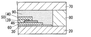
有機エレクトロルミネッセンス素子は、第1電極を兼ねる基材20と、基材20の一表面側にあり少なくとも発光層32を含む機能層30と、機能層30における基材20側とは反対側にある第2電極50とを備えている。   The organic electroluminescence element is on the base 20 that also serves as the first electrode, the functional layer 30 that is on one surface side of the base 20 and includes at least the light emitting layer 32, and the functional layer 30 on the side opposite to the base 20 side. And a second electrode 50.

また、有機エレクトロルミネッセンス素子は、基材20の上記一表面側において第2電極50に電気的に接続された引き出し電極部47と、引き出し電極部47と基材20とを電気的に絶縁する絶縁層60とを備えている。ここにおいて、有機エレクトロルミネッセンス素子は、第2電極50に電気的に接続された矩形枠状の補助電極46を備えており、引き出し電極部47は、補助電極46から延設されている。   In addition, the organic electroluminescence element includes an extraction electrode portion 47 that is electrically connected to the second electrode 50 on the one surface side of the substrate 20, and an insulation that electrically insulates the extraction electrode portion 47 and the substrate 20. Layer 60. Here, the organic electroluminescence element includes a rectangular frame-shaped auxiliary electrode 46 electrically connected to the second electrode 50, and the extraction electrode portion 47 extends from the auxiliary electrode 46.

また、有機エレクトロルミネッセンス素子は、第2電極50における機能層30側とは反対側にあり透光性を有する封止部材70と、第2電極50と封止部材70との間に介在する透光性の樹脂層90と、基材20の周部と封止部材70の周部との間にある枠状の封止部80とを備えている。ここにおいて、有機エレクトロルミネッセンス素子は、封止部材70側から光を取り出すものである。要するに、有機エレクトロルミネッセンス素子は、第2電極50側から樹脂層90および封止部材70を通して光を取り出すものである。   In addition, the organic electroluminescence element is on the side opposite to the functional layer 30 side of the second electrode 50 and has a light-transmitting sealing member 70 and a transparent member interposed between the second electrode 50 and the sealing member 70. An optical resin layer 90 and a frame-shaped sealing portion 80 between the peripheral portion of the substrate 20 and the peripheral portion of the sealing member 70 are provided. Here, the organic electroluminescence element extracts light from the sealing member 70 side. In short, the organic electroluminescence element extracts light from the second electrode 50 side through the resin layer 90 and the sealing member 70.

機能層30は、基材20の上記一表面における規定方向(図1(a)の左右方向)に沿った2辺間に亘って形成され、且つ、上記一表面における上記規定方向に直交する2辺から離れて形成されている。ここにおいて、機能層30は、塗布法により形成してあり、上記規定方向に直交する方向に沿って塗布されている。   The functional layer 30 is formed between two sides along the prescribed direction (the left-right direction in FIG. 1A) on the one surface of the substrate 20 and is orthogonal to the prescribed direction on the one surface. It is formed away from the side. Here, the functional layer 30 is formed by a coating method, and is applied along a direction orthogonal to the prescribed direction.

基材20は、上記一表面において上記規定方向に直交する方向の両端部が機能層30の各一部と併せて封止部材70側へ折り返され、当該折り返された両端部では他表面が封止部80と接着されている。また、引き出し電極部47は、上記規定方向に沿って封止部80の外側へ引き出されている。   The base material 20 has both ends in a direction perpendicular to the specified direction on one surface folded together with each part of the functional layer 30 toward the sealing member 70, and the other surface sealed at the folded both ends. The stopper 80 is bonded. Further, the extraction electrode portion 47 is extracted to the outside of the sealing portion 80 along the prescribed direction.

本実施形態の有機エレクトルミネッセンス素子における基材20は、上記規定方向の両端部で引き出し電極部47が形成された第1部分20aが、封止部材70側とは反対側へ折り返されている(図1(c)参照)。図1(c)は、図1(a)のC−C’線およびE−E’線に沿った概略断面図であり、第1部分20aを含む概略断面図である。基材20は、上記規定方向の両端部の少なくとも一方で、引き出し電極部47が形成された第1部分20aが、封止部材70側とは反対側へ折り返されていればよい。なお、基材20の上記一表面における上記規定方向の両端部の第1部分20a以外の第2部分については、後述する。   In the base material 20 in the organic electroluminescence element of the present embodiment, the first portion 20a in which the extraction electrode portion 47 is formed at both end portions in the specified direction is folded back to the side opposite to the sealing member 70 side ( (Refer FIG.1 (c)). FIG. 1C is a schematic cross-sectional view taken along lines C-C ′ and E-E ′ of FIG. 1A, and is a schematic cross-sectional view including the first portion 20 a. In the base material 20, it is only necessary that the first portion 20 a on which the extraction electrode portion 47 is formed is folded back to the side opposite to the sealing member 70 side at at least one of both ends in the specified direction. In addition, 2nd parts other than the 1st part 20a of the both ends of the said prescribed direction in the said one surface of the base material 20 are mentioned later.

また、基材20は、上記一表面において上記規定方向に直交する方向の両端部(第3部分20c)が、封止部材70側へ折り返されている(図1(b)参照)。図1(b)は、図1(a)のA−A’線、D−D’線に沿った共通の概略断面図であり、第3部分20cを含む概略断面図である。   Moreover, as for the base material 20, the both ends (3rd part 20c) of the direction orthogonal to the said prescription | regulation direction in the said one surface are return | folded by the sealing member 70 side (refer FIG.1 (b)). FIG. 1B is a common schematic cross-sectional view taken along lines A-A ′ and D-D ′ in FIG. 1A, and is a schematic cross-sectional view including the third portion 20 c.

また、封止部80は、封止部材70とは反対側において、引き出し電極部47の一部に接着された第1部位80a以外の第2部位80bが、基材20の他表面に接着されている。要するに、封止部80は、封止部材70とは反対側に、基材20の上記一表面側にある各引き出し電極部47の各々に接着された第1部位80aと、基材20の他表面に接着された第2部位80bとを有している。引き出し電極部47のうち封止部80よりも外側にある部分は、保護層91により保護されており、保護層91に設けられた開口部92により露出した部分が、外部接続用の端子部48を構成している。   Further, on the side opposite to the sealing member 70, the second portion 80 b other than the first portion 80 a bonded to a part of the extraction electrode portion 47 is bonded to the other surface of the base member 20. ing. In short, the sealing portion 80 includes, on the opposite side to the sealing member 70, the first portion 80 a bonded to each of the lead electrode portions 47 on the one surface side of the base material 20, and the other of the base material 20. And a second portion 80b bonded to the surface. A portion of the lead electrode portion 47 outside the sealing portion 80 is protected by the protective layer 91, and a portion exposed by the opening 92 provided in the protective layer 91 is a terminal portion 48 for external connection. Is configured.

上述の第2電極50は、機能層30からの光を取り出すことが可能となるように構成されている。第2電極50は、機能層30に接する導電性高分子層39と、この導電性高分子層39における機能層30側とは反対側に位置し機能層30からの光の取り出し用の開口部41(図2および図3参照)を有する電極パターン40とを備えていることが好ましい。要するに、有機エレクトロルミネッセンス素子は、第2電極50が、機能層30からの光の取り出し用の開口部41を有していることが好ましい。   The second electrode 50 described above is configured so that light from the functional layer 30 can be extracted. The second electrode 50 includes a conductive polymer layer 39 that is in contact with the functional layer 30, and an opening for extracting light from the functional layer 30 that is located on the opposite side of the conductive polymer layer 39 from the functional layer 30 side. And electrode pattern 40 having 41 (see FIGS. 2 and 3). In short, in the organic electroluminescence element, it is preferable that the second electrode 50 has an opening 41 for extracting light from the functional layer 30.

有機エレクトロルミネッセンス素子は、第1電極を兼ねる基材20および第2電極50の電極パターン40それぞれの抵抗率を、透明導電性酸化物(Transparent Conducting Oxide:TCO)の抵抗率よりも低くしてある。透明導電性酸化物としては、例えば、ITO、AZO、GZO、IZOなどがある。   In the organic electroluminescence element, the resistivity of each of the electrode pattern 40 of the base material 20 that also serves as the first electrode and the second electrode 50 is made lower than the resistivity of the transparent conductive oxide (TCO). . Examples of the transparent conductive oxide include ITO, AZO, GZO, and IZO.

樹脂層90は、基材20と封止部材70と封止部80とで囲まれる空間において、第1電極、機能層30および第2電極50などからなる素子部を覆うように設けることが好ましい。また、樹脂層90は、導電性高分子層39の屈折率以上の屈折率を有することが好ましい。   The resin layer 90 is preferably provided so as to cover the element portion including the first electrode, the functional layer 30, the second electrode 50, and the like in a space surrounded by the base material 20, the sealing member 70, and the sealing portion 80. . The resin layer 90 preferably has a refractive index that is equal to or higher than the refractive index of the conductive polymer layer 39.

以下、有機エレクトロルミネッセンス素子の各構成要素について詳細に説明する。   Hereinafter, each component of the organic electroluminescence element will be described in detail.

基材20は、平面形状を矩形状としてあるが、矩形状であれば、長方形状でも正方形状でもよい。   The substrate 20 has a rectangular planar shape, but may be rectangular or square as long as it is rectangular.

基材20は、金属箔により構成してある。金属箔からなる基材20の上記一表面の表面粗さについては、JIS B 0601−2001(ISO 4287−1997)で規定されている算術平均粗さRaが10nm以下であることが好ましく、数nm以下であることが、より好ましい。これにより、第1電極を兼ねる基材20の上記一表面の表面粗さに起因して、第1電極を兼ねる基材20と第2電極50との短絡を抑制することが可能となる。   The base material 20 is comprised with the metal foil. Regarding the surface roughness of the one surface of the base material 20 made of metal foil, the arithmetic average roughness Ra defined by JIS B 0601-2001 (ISO 4287-1997) is preferably 10 nm or less, and several nm. The following is more preferable. Thereby, it becomes possible to suppress a short circuit between the base material 20 also serving as the first electrode and the second electrode 50 due to the surface roughness of the one surface of the base material 20 also serving as the first electrode.

金属箔の材料としては、例えば、銅、ステンレス鋼、アルミニウム、ニッケル、錫、鉛、金、銀、鉄、チタンなどの金属や、これらの金属の1種以上を含む合金などを採用することができる。ただし、本実施形態では、第1電極が反射電極となるので、発光層32から放射される光に対する反射率が高く、且つ、抵抗率の低い材料が好ましい。また、金属箔の材料としては、耐候性の高い材料が好ましい。   As a material of the metal foil, for example, a metal such as copper, stainless steel, aluminum, nickel, tin, lead, gold, silver, iron, titanium, or an alloy containing one or more of these metals may be employed. it can. However, in the present embodiment, since the first electrode serves as a reflective electrode, a material having a high reflectance with respect to light emitted from the light emitting layer 32 and a low resistivity is preferable. Moreover, as a material of metal foil, a material with high weather resistance is preferable.

本実施形態の有機エレクトロルミネッセンス素子では、第1電極が陰極を構成し、第2電極50が陽極を構成している。この場合、第1電極から機能層30へ注入する第1キャリアは電子であり、第2電極50から機能層30へ注入する第2キャリアは正孔である。機能層30は、第1電極側から順に、第1キャリア注入層31、発光層32、第2キャリア輸送層33、第2キャリア注入層34を備えている。ここにおいて、第1キャリア注入層31、第2キャリア輸送層33、第2キャリア注入層34は、それぞれ、電子注入層、ホール輸送層、ホール注入層である。なお、第1電極が陽極を構成し、第2電極50が陰極を構成する場合には、例えば、第1キャリア注入層31としてホール注入層を、第2キャリア輸送層33として電子輸送層を、第2キャリア注入層34として電子注入層を採用すればよい。   In the organic electroluminescence element of the present embodiment, the first electrode constitutes a cathode and the second electrode 50 constitutes an anode. In this case, the first carrier injected from the first electrode into the functional layer 30 is an electron, and the second carrier injected from the second electrode 50 into the functional layer 30 is a hole. The functional layer 30 includes a first carrier injection layer 31, a light emitting layer 32, a second carrier transport layer 33, and a second carrier injection layer 34 in this order from the first electrode side. Here, the first carrier injection layer 31, the second carrier transport layer 33, and the second carrier injection layer 34 are an electron injection layer, a hole transport layer, and a hole injection layer, respectively. When the first electrode constitutes an anode and the second electrode 50 constitutes a cathode, for example, a hole injection layer as the first carrier injection layer 31, an electron transport layer as the second carrier transport layer 33, An electron injection layer may be employed as the second carrier injection layer 34.

上述の機能層30の構造は、図1の例に限らず、例えば、第1キャリア注入層31と発光層32との間に、第1キャリア輸送層を設けたり、発光層32と第2キャリア注入層34との間にインターレイヤーを設けたりした構造でもよい。第1電極が陰極を構成し、第2電極50が陽極を構成している場合、第2キャリア輸送層は、ホール輸送層である。   The structure of the functional layer 30 described above is not limited to the example of FIG. 1. For example, a first carrier transport layer is provided between the first carrier injection layer 31 and the light emitting layer 32, or the light emitting layer 32 and the second carrier are provided. A structure in which an interlayer is provided between the injection layer 34 and the injection layer 34 may be used. When the first electrode constitutes a cathode and the second electrode 50 constitutes an anode, the second carrier transport layer is a hole transport layer.

また、機能層30は、少なくとも発光層32を含んでいればよく(つまり、機能層30は、発光層32のみでもよく)、発光層32以外の、第1キャリア注入層31、第1キャリア輸送層、インターレイヤー、第2キャリア輸送層33、第2キャリア注入層34などは適宜設ければよい。発光層32は、単層構造でも多層構造でもよい。例えば、所望の発光色が白色の場合には、発光層32中に赤色、緑色、青色の3種類のドーパント色素をドーピングするようにしてもよいし、青色正孔輸送性発光層と緑色電子輸送性発光層と赤色電子輸送性発光層との積層構造を採用してもよいし、青色電子輸送性発光層と緑色電子輸送性発光層と赤色電子輸送性発光層との積層構造を採用してもよい。   Further, the functional layer 30 only needs to include at least the light emitting layer 32 (that is, the functional layer 30 may be only the light emitting layer 32), and the first carrier injection layer 31 and the first carrier transport other than the light emitting layer 32 may be used. The layer, the interlayer, the second carrier transport layer 33, the second carrier injection layer 34, and the like may be provided as appropriate. The light emitting layer 32 may have a single layer structure or a multilayer structure. For example, when the desired emission color is white, the light emitting layer 32 may be doped with three kinds of dopant dyes of red, green, and blue, or the blue hole transporting light emitting layer and the green electron transport. A laminated structure of a light emitting layer and a red electron transporting light emitting layer may be adopted, or a laminated structure of a blue electron transporting light emitting layer, a green electron transporting light emitting layer and a red electron transporting light emitting layer may be adopted. Also good.

発光層32の材料としては、例えば、ポリパラフェニレンビニレン誘導体、ポリチオフェン誘導体、ポリパラフェニレン誘導体、ポリシラン誘導体、ポリアセチレン誘導体など、ポリフルオレン誘導体、ポリビニルカルバゾール誘導体、色素体、金属錯体系発光材料を高分子化したものなどや、アントラセン、ナフタレン、ピレン、テトラセン、コロネン、ペリレン、フタロペリレン、ナフタロペリレン、ジフェニルブタジエン、テトラフェニルブタジエン、クマリン、オキサジアゾール、ビスベンゾキサゾリン、ビススチリル、シクロペンタジエン、クマリン、オキサジアゾール、ビスベンゾキサゾリン、ビススチリル、シクロペンタジエン、キノリン金属錯体、トリス(8−ヒドロキシキノリナート)アルミニウム錯体、トリス(4−メチル−8−キノリナート)アルミニウム錯体、トリス(5−フェニル−8−キノリナート)アルミニウム錯体、アミノキノリン金属錯体、ベンゾキノリン金属錯体、トリ−(p−ターフェニル−4−イル)アミン、ピラン、キナクリドン、ルブレン、およびこれらの誘導体、あるいは、1−アリール−2,5−ジ(2−チエニル)ピロール誘導体、ジスチリルベンゼン誘導体、スチリルアリーレン誘導体、スチリルアミン誘導体、およびこれらの発光性化合物からなる基を分子の一部分に有する化合物などが挙げられる。また、上記化合物に代表される蛍光色素由来の化合物のみならず、いわゆる燐光発光材料、例えばイリジウム錯体、オスミウム錯体、白金錯体、ユーロピウム錯体などの発光材料、又はそれらを分子内に有する化合物若しくは高分子も好適に用いることができる。これらの材料は、必要に応じて、適宜選択して用いることができる。発光層32は、塗布法(例えば、スピンコート法、スプレーコート法、ダイコート法、グラビア印刷法、スクリーン印刷法など)のような湿式プロセスによって成膜することが好ましい。ただし、発光層32の成膜方法は、塗布法に限らず、例えば、真空蒸着法、転写法などの乾式プロセスによって発光層32を成膜してもよい。   Examples of the material of the light emitting layer 32 include polyparaphenylene vinylene derivatives, polythiophene derivatives, polyparaphenylene derivatives, polysilane derivatives, polyacetylene derivatives, polyfluorene derivatives, polyvinylcarbazole derivatives, dye bodies, and metal complex light emitting materials. Anthracene, naphthalene, pyrene, tetracene, coronene, perylene, phthaloperylene, naphthaloperylene, diphenylbutadiene, tetraphenylbutadiene, coumarin, oxadiazole, bisbenzoxazoline, bisstyryl, cyclopentadiene, coumarin, oxadiazole , Bisbenzoxazoline, bisstyryl, cyclopentadiene, quinoline metal complex, tris (8-hydroxyquinolinato) aluminum complex, tris (4-mes Ru-8-quinolinato) aluminum complex, tris (5-phenyl-8-quinolinato) aluminum complex, aminoquinoline metal complex, benzoquinoline metal complex, tri- (p-terphenyl-4-yl) amine, pyran, quinacridone, Rubrene, and derivatives thereof, or 1-aryl-2,5-di (2-thienyl) pyrrole derivatives, distyrylbenzene derivatives, styrylarylene derivatives, styrylamine derivatives, and groups comprising these luminescent compounds are molecules And the like. Further, not only compounds derived from fluorescent dyes typified by the above compounds, but also so-called phosphorescent materials, for example, luminescent materials such as iridium complexes, osmium complexes, platinum complexes, europium complexes, or compounds or polymers having these in the molecule Can also be suitably used. These materials can be appropriately selected and used as necessary. The light emitting layer 32 is preferably formed by a wet process such as a coating method (for example, spin coating method, spray coating method, die coating method, gravure printing method, screen printing method, etc.). However, the method for forming the light emitting layer 32 is not limited to the coating method, and the light emitting layer 32 may be formed by a dry process such as a vacuum deposition method or a transfer method.

電子注入層の材料は、例えば、フッ化リチウムやフッ化マグネシウムなどの金属フッ化物、塩化ナトリウム、塩化マグネシウムなどに代表される金属塩化物などの金属ハロゲン化物や、チタン、亜鉛、マグネシウム、カルシウム、バリウム、ストロンチウムなどの酸化物、などを用いることができる。これらの材料の場合、電子注入層は、真空蒸着法により形成することができる。また、電子注入層の材料は、例えば、電子注入を促進させるドーパント(アルカリ金属など)を混合した有機半導体材料を用いることができる。このような材料の場合、電子注入層は、塗布法により形成することができる。   Examples of the material for the electron injection layer include metal fluorides such as lithium fluoride and magnesium fluoride, metal halides such as sodium chloride and magnesium chloride, titanium, zinc, magnesium, calcium, An oxide such as barium or strontium can be used. In the case of these materials, the electron injection layer can be formed by a vacuum deposition method. As the material for the electron injection layer, for example, an organic semiconductor material mixed with a dopant (such as an alkali metal) that promotes electron injection can be used. In the case of such a material, the electron injection layer can be formed by a coating method.

また、電子輸送層の材料は、電子輸送性を有する化合物の群から選定することができる。この種の化合物としては、Alq等の電子輸送性材料として知られる金属錯体や、フェナントロリン誘導体、ピリジン誘導体、テトラジン誘導体、オキサジアゾール誘導体などのヘテロ環を有する化合物などが挙げられるが、この限りではなく、一般に知られる任意の電子輸送材料を用いることが可能である。 The material for the electron transport layer can be selected from the group of compounds having electron transport properties. Examples of this type of compound include metal complexes known as electron transporting materials such as Alq 3 and compounds having a heterocyclic ring such as phenanthroline derivatives, pyridine derivatives, tetrazine derivatives, and oxadiazole derivatives. Instead, any generally known electron transport material can be used.

ホール輸送層の材料としては、LUMO(Lowest UnoccupiedMolecular Orbital)準位が小さい低分子材料や高分子材料を用いることができる。例えば、ポリビニルカルバゾール(PVCz)や、ポリピリジン、ポリアニリンなどの側鎖や主鎖に芳香族アミンを有するポリアリーレン誘導体などの芳香族アミンを含むポリマーなどが挙げられるが、これらに限定されるものではない。なお、ホール輸送層の材料としては、例えば、4,4’−ビス[N−(ナフチル)−N−フェニル−アミノ]ビフェニル(α−NPD)、N,N’−ビス(3−メチルフェニル)−(1,1’−ビフェニル)−4,4’−ジアミン(TPD)、2−TNATA、4,4’,4”−トリス(N−(3−メチルフェニル)N−フェニルアミノ)トリフェニルアミン(MTDATA)、4,4’−N,N’−ジカルバゾールビフェニル(CBP)、スピロ−NPD、スピロ−TPD、スピロ−TAD、TNBなどを用いることが可能である。   As a material for the hole transport layer, a low molecular material or a polymer material having a low LUMO (Lowest Unoccupied Molecular Orbital) level can be used. Examples thereof include polymers containing aromatic amines such as polyvinyl carbazole (PVCz), polyarylene derivatives such as polypyridine and polyaniline, and polyarylene derivatives having aromatic amines in the main chain, but are not limited thereto. . In addition, as a material of the hole transport layer, for example, 4,4′-bis [N- (naphthyl) -N-phenyl-amino] biphenyl (α-NPD), N, N′-bis (3-methylphenyl) -(1,1'-biphenyl) -4,4'-diamine (TPD), 2-TNATA, 4,4 ', 4 "-tris (N- (3-methylphenyl) N-phenylamino) triphenylamine (MTDATA), 4,4′-N, N′-dicarbazole biphenyl (CBP), spiro-NPD, spiro-TPD, spiro-TAD, TNB, and the like can be used.

ホール注入層の材料としては、例えば、チオフェン、トリフェニルメタン、ヒドラゾリン、アミールアミン、ヒドラゾン、スチルベン、トリフェニルアミンなどを含む有機材料が挙げられる。具体的には、たとえば、ポリビニルカルバゾール、ポリエチレンジオキシチオフェン:ポリスチレンスルホネート(PEDOT:PSS)、TPDなどの芳香族アミン誘導体などで、これらの材料を単独で用いてもよいし、2種類以上の材料を組み合わせて用いてもよい。このようなホール注入層は、塗布法(スピンコート法、スプレーコート法、ダイコート法、グラビア印刷法など)のような湿式プロセスによって成膜することができる。   Examples of the material for the hole injection layer include organic materials including thiophene, triphenylmethane, hydrazoline, amiramine, hydrazone, stilbene, triphenylamine, and the like. Specifically, for example, polyvinyl carbazole, polyethylenedioxythiophene: polystyrene sulfonate (PEDOT: PSS), aromatic amine derivatives such as TPD, etc., these materials may be used alone, or two or more kinds of materials. May be used in combination. Such a hole injection layer can be formed by a wet process such as a coating method (spin coating method, spray coating method, die coating method, gravure printing method, etc.).

インターレイヤーは、発光層32側からの第2電極50側への第1キャリア(ここでは、電子)の漏れを抑制する第1キャリア障壁(ここでは、電子障壁)としてのキャリアブロッキング機能(ここでは、電子ブロッキング機能)を有することが好ましく、更に、第2キャリア(ここでは、正孔)を発光層32へ輸送する機能、発光層32の励起状態の消光を抑制する機能などを有していることが好ましい。なお、本実施形態では、インターレイヤーが、発光層32側からの電子の漏れを抑制する電子ブロッキング層を構成している。   The interlayer is a carrier blocking function (here, an electron barrier) that suppresses leakage of first carriers (here, electrons) from the light emitting layer 32 side to the second electrode 50 side. , An electron blocking function), and further has a function of transporting second carriers (here, holes) to the light emitting layer 32, a function of suppressing quenching of the excited state of the light emitting layer 32, and the like. It is preferable. In the present embodiment, the interlayer constitutes an electron blocking layer that suppresses leakage of electrons from the light emitting layer 32 side.

有機エレクトロルミネッセンス素子では、インターレイヤーを設けることにより、発光効率の向上および長寿命化を図ることが可能となる。インターレイヤーの材料としては、例えば、ポリアリールアミン若しくはその誘導体、ポリフルオレン若しくはその誘導体、ポリビニルカルバゾール若しくはその誘導体、トリフェニルジアミン誘導体などを用いることができる。このようなインターレイヤーは、塗布法(スピンコート法、スプレーコート法、ダイコート法、グラビア印刷法など)のような湿式プロセスによって成膜することができる。   In the organic electroluminescence element, by providing an interlayer, it is possible to improve the light emission efficiency and extend the life. As an interlayer material, for example, polyarylamine or a derivative thereof, polyfluorene or a derivative thereof, polyvinylcarbazole or a derivative thereof, a triphenyldiamine derivative, or the like can be used. Such an interlayer can be formed by a wet process such as a coating method (spin coating method, spray coating method, die coating method, gravure printing method, or the like).

また、陰極は、機能層30中に第1電荷である電子(第1キャリア)を注入するための電極である。第1電極が陰極の場合、陰極の材料としては、仕事関数の小さい金属、合金、電気伝導性化合物およびこれらの混合物からなる電極材料を用いることが好ましく、LUMO(Lowest Unoccupied Molecular Orbital)準位との差が大きくなりすぎないように仕事関数が1.9eV以上5eV以下のものを用いるのが好ましい。なお、第1電極が、機能層30中に第2電荷であるホール(第2キャリア)を注入するための電極である陽極を構成する場合、第1電極の材料としては、仕事関数の大きい金属を用いることが好ましく、HOMO(Highest Occupied Molecular Orbital)準位との差が大きくなりすぎないように仕事関数が4eV以上6eV以下のものを用いるのが好ましい。   The cathode is an electrode for injecting electrons (first carriers) that are first charges into the functional layer 30. When the first electrode is a cathode, it is preferable to use an electrode material made of a metal, an alloy, an electrically conductive compound and a mixture thereof having a low work function as the cathode material, and the LUMO (Lowest Unoccupied Molecular Orbital) level It is preferable to use a work function having a work function of 1.9 eV or more and 5 eV or less so that the difference between them is not too large. When the first electrode constitutes an anode that is an electrode for injecting holes (second carriers) that are second charges into the functional layer 30, the material of the first electrode is a metal having a high work function. Is preferably used, and a work function of 4 eV or more and 6 eV or less is preferably used so that the difference from the HOMO (Highest Occupied Molecular Orbital) level does not become too large.

第2電極50の導電性高分子層39の材料としては、例えば、ポリチオフェン、ポリアニリン、ポリピロール、ポリフェニレン、ポリフェニレンビニレン、ポリアセチレン、ポリカルバゾールなどの導電性高分子材料を用いることができる。また、導電性高分子層39の導電性高分子材料としては、導電性を高めるために、例えば、スルホン酸、ルイス酸、プロトン酸、アルカリ金属、アルカリ土類金属などのドーパントをドーピングしたものを採用してもよい。ここで、導電性高分子層39は、抵抗率がより低いほうが好ましく、抵抗率が低いほど、横方向(面内方向)への通電性が向上し、発光層32に流れる電流の面内ばらつきを低減することが可能となり、輝度むらを低減することが可能となる。   As a material of the conductive polymer layer 39 of the second electrode 50, for example, a conductive polymer material such as polythiophene, polyaniline, polypyrrole, polyphenylene, polyphenylene vinylene, polyacetylene, polycarbazole can be used. In addition, as the conductive polymer material of the conductive polymer layer 39, for example, a material doped with a dopant such as sulfonic acid, Lewis acid, proton acid, alkali metal, alkaline earth metal, etc. in order to increase conductivity. It may be adopted. Here, it is preferable that the conductive polymer layer 39 has a lower resistivity. The lower the resistivity, the better the conductivity in the lateral direction (in-plane direction), and the in-plane variation of the current flowing through the light emitting layer 32. Can be reduced, and uneven brightness can be reduced.

第2電極50の電極パターン40は、金属の粉末と有機バインダとを含む電極からなる。この種の金属としては、例えば、銀、金、銅などを採用することができる。これにより、有機エレクトロルミネッセンス素子は、第2電極50が、導電性透明酸化物により形成された薄膜の場合に比べて、第2電極50の電極パターン40の抵抗率およびシート抵抗を小さくすることが可能となり、輝度むらを低減することが可能となる。なお、第2電極50の電極パターン40の導電性材料としては、金属の代わりに、合金や、カーボンブラックなどを用いることも可能である。   The electrode pattern 40 of the second electrode 50 is made of an electrode containing metal powder and an organic binder. As this type of metal, for example, silver, gold, copper or the like can be employed. Thereby, the organic electroluminescence element can reduce the resistivity and the sheet resistance of the electrode pattern 40 of the second electrode 50 as compared with the case where the second electrode 50 is a thin film formed of a conductive transparent oxide. This makes it possible to reduce uneven brightness. In addition, as a conductive material of the electrode pattern 40 of the second electrode 50, an alloy, carbon black, or the like can be used instead of a metal.

電極パターン40は、例えば、金属の粉末に有機バインダおよび有機溶剤を混合させたペースト(印刷インク)を、例えばスクリーン印刷法、グラビア印刷法などにより印刷して形成することができる。有機バインダとしては、例えば、アクリル樹脂、ポリエチレン、ポリプロピレン、ポリエチレンテレフタレート、ポリメチルメタクリレート、ポリスチレン、ポリエーテルスルホン、ポリアリレート、ポリカーボネート樹脂、ポリウレタン、ポリアクリルニトリル、ポリビニルアセタール、ポリアミド、ポリイミド、ジアクリルフタレート樹脂、セルロース系樹脂、ポリ塩化ビニル、ポリ塩化ビニリデン、ポリ酢酸ビニル、その他の熱可塑性樹脂や、これらの樹脂を構成する単量体の2種以上の共重合体が挙げられるが、これらに限定されるものではない。   The electrode pattern 40 can be formed, for example, by printing a paste (printing ink) in which an organic binder and an organic solvent are mixed with metal powder by, for example, a screen printing method or a gravure printing method. Examples of the organic binder include acrylic resin, polyethylene, polypropylene, polyethylene terephthalate, polymethyl methacrylate, polystyrene, polyether sulfone, polyarylate, polycarbonate resin, polyurethane, polyacrylonitrile, polyvinyl acetal, polyamide, polyimide, and diacryl phthalate resin. , Cellulose resins, polyvinyl chloride, polyvinylidene chloride, polyvinyl acetate, other thermoplastic resins, and copolymers of two or more monomers constituting these resins, but are not limited thereto. It is not something.

電極パターン40は、図1〜図3に示すように、格子状(網状)に形成されており、複数(図3に示した例では、6×6=36)の開口部41を有している。ここで、図3に示した電極パターン40は、各開口部41の各々の平面視形状が正方形状である。要するに、図3に示した電極パターン40は、正方格子状に形成されている。   1 to 3, the electrode pattern 40 is formed in a lattice shape (mesh shape), and has a plurality of openings 41 (6 × 6 = 36 in the example shown in FIG. 3). Yes. Here, in the electrode pattern 40 shown in FIG. 3, each planar view shape of each opening 41 is a square shape. In short, the electrode pattern 40 shown in FIG. 3 is formed in a square lattice shape.

第2電極50は、正方格子状の電極パターン40の寸法に関して、例えば、線幅L1(図2参照)を1μm〜100μm、高さH1(図2参照)を50nm〜100μm、ピッチP1(図2参照)を100μm〜2000μmとすればよい。ただし、第2電極50の電極パターン40の線幅L1、高さH1およびピッチP1それぞれの数値範囲は、特に限定するものではなく、素子部の平面サイズに基づいて適宜設定すればよい。ここにおいて、第2電極50の電極パターン40の線幅L1については、発光層32で発光する光の利用効率の観点からは狭い方が好ましく、第2電極50の低抵抗化によって輝度むらを低減するという観点からは広い方が好ましいので、有機エレクトロルミネッセンス素子の平面サイズなどに基づいて適宜設定することが好ましい。また、第2電極50の電極パターン40の高さH1については、第2電極50の低抵抗化の観点、電極パターン40をスクリーン印刷法などの塗布法により形成する際の電極パターン40の材料の使用効率(材料使用効率)の観点、機能層30から放射される光の放射角の観点などから、100nm以上10μm以下が、より好ましい。   Regarding the dimensions of the square grid electrode pattern 40, for example, the second electrode 50 has a line width L1 (see FIG. 2) of 1 μm to 100 μm, a height H1 (see FIG. 2) of 50 nm to 100 μm, and a pitch P1 (FIG. 2). Reference) may be set to 100 μm to 2000 μm. However, the numerical ranges of the line width L1, the height H1, and the pitch P1 of the electrode pattern 40 of the second electrode 50 are not particularly limited, and may be set as appropriate based on the planar size of the element portion. Here, the line width L1 of the electrode pattern 40 of the second electrode 50 is preferably narrow from the viewpoint of the utilization efficiency of the light emitted from the light emitting layer 32, and luminance unevenness is reduced by reducing the resistance of the second electrode 50. Therefore, it is preferable that the width is appropriately set based on the planar size of the organic electroluminescence element. Further, regarding the height H1 of the electrode pattern 40 of the second electrode 50, from the viewpoint of reducing the resistance of the second electrode 50, the material of the electrode pattern 40 when the electrode pattern 40 is formed by a coating method such as a screen printing method is used. 100 nm or more and 10 micrometers or less are more preferable from a viewpoint of use efficiency (material use efficiency), a viewpoint of the radiation angle of the light radiated | emitted from the functional layer 30, etc.

また、本実施形態の有機エレクトロルミネッセンス素子では、電極パターン40における各開口部41を、図2に示したように、機能層30から離れるにつれて開口面積が徐々に大きくなる開口形状としてある。これにより、有機エレクトロルミネッセンス素子は、機能層30から放射される光の広がり角を大きくすることが可能になり、輝度むらを、より低減することが可能となる。また、有機エレクトロルミネッセンス素子は、第2電極50の電極パターン40での反射損失や吸収損失を低減することが可能となり、外部量子効率のより一層の向上を図ることが可能となる。   In the organic electroluminescence element of this embodiment, each opening 41 in the electrode pattern 40 has an opening shape in which the opening area gradually increases as the distance from the functional layer 30 increases, as shown in FIG. Thereby, the organic electroluminescence element can increase the spread angle of the light emitted from the functional layer 30, and can further reduce the luminance unevenness. In addition, the organic electroluminescence element can reduce reflection loss and absorption loss at the electrode pattern 40 of the second electrode 50, and can further improve the external quantum efficiency.

電極パターン40を格子状の形状とする場合、各開口部41の各々の平面視形状は正方形状に限らず、例えば、長方形状や正三角形状や正六角形状の形状としてもよい。   When the electrode pattern 40 has a lattice shape, the shape of each opening 41 in plan view is not limited to a square shape, and may be, for example, a rectangular shape, a regular triangle shape, or a regular hexagonal shape.

電極パターン40は、各開口部41の各々の平面視形状が正三角形状の場合、三角格子状の形状となり、各開口部41の各々の平面視形状が正六角形状の場合、六角格子状の形状となる。なお、電極パターン40は、格子状の形状に限らず、例えば、櫛形状の形状でもよいし、2つの櫛形状の電極パターンにより構成してもよい。また、電極パターン40は、開口部41の数も特に限定するものではなく、複数に限らず、1つでもよい。例えば、電極パターン40を櫛形状の形状としたり、2つの櫛形状の電極パターンにより構成とした場合などは、開口部41の数を1つとすることが可能である。   The electrode pattern 40 has a triangular lattice shape when each opening 41 has a regular triangular shape, and has a hexagonal lattice shape when each opening 41 has a regular hexagonal shape. It becomes a shape. The electrode pattern 40 is not limited to the lattice shape, and may be, for example, a comb shape or may be configured by two comb electrode patterns. Further, the number of the opening portions 41 is not particularly limited, and the electrode pattern 40 is not limited to a plurality and may be one. For example, when the electrode pattern 40 has a comb shape or is constituted by two comb-shaped electrode patterns, the number of openings 41 can be one.

また、電極パターン40は、例えば、図4に示すような平面形状としてもよい。すなわち、電極パターン40は、平面視において、直線状の細線部44の線幅を一定として、電極パターン40における周部から中心部に近づくにつれて隣り合う細線部44間の間隔が狭くなり開口部41の開口面積が小さくなる形状としてもよい。有機エレクトロルミネッセンス素子は、第2電極50の電極パターン40の平面形状を図4のような平面形状とすることにより、図3のような平面形状とした場合に比べて、第2電極50において引き出し電極部47(図1参照)からの距離が周部よりも遠い中央部での発光効率を向上させることが可能となり、外部量子効率の向上を図ることが可能となる。また、有機エレクトロルミネッセンス素子は、第2電極50の電極パターン40の平面形状を図4のような形状とすることにより、図3のような平面形状とした場合に比べて、機能層30のうち引き出し電極部47からの距離が近い周部での電流集中を抑制することが可能となるから、長寿命化を図ることが可能となる。   Further, the electrode pattern 40 may have a planar shape as shown in FIG. 4, for example. That is, in the electrode pattern 40, the line width of the linear thin line portion 44 is constant in a plan view, and the interval between the adjacent thin line portions 44 becomes narrower as the distance from the peripheral portion to the center portion of the electrode pattern 40 decreases. The opening area may be reduced. The organic electroluminescence element is drawn out in the second electrode 50 by making the planar shape of the electrode pattern 40 of the second electrode 50 into a planar shape as shown in FIG. 4, compared with the planar shape as shown in FIG. It becomes possible to improve the light emission efficiency in the center part where the distance from the electrode part 47 (refer FIG. 1) is far from a peripheral part, and it becomes possible to aim at the improvement of external quantum efficiency. Further, the organic electroluminescence element has a functional shape of the functional layer 30 as compared with the planar shape as shown in FIG. 3 by making the planar shape of the electrode pattern 40 of the second electrode 50 as shown in FIG. Since it is possible to suppress current concentration in the peripheral portion where the distance from the extraction electrode portion 47 is short, it is possible to extend the life.

また、第2電極50の電極パターン40は、例えば、図5に示すような平面形状としてもよい。すなわち、電極パターン40は、平面視において、電極パターン40における最外周にある4つの第1細線部42の線幅と、図5において左右方向の中央にある1つの第2細線部43の線幅とを、第1細線部42と第2細線部43との間にある細線部(第3細線部)44よりも幅広としてある。有機エレクトロルミネッセンス素子は、第2電極50の電極パターン40を図5のような平面形状とすることにより、図3のような平面形状の場合に比べて、第2電極50において引き出し電極部47(図1参照)からの距離が周部よりも遠い中央部での発光効率を向上させることが可能となり、外部量子効率の向上を図ることが可能となる。なお、電極パターン40は、図5のような平面形状とする場合、相対的に線幅の広い第1細線部42および第2細線部43の高さを第3細線部44の高さよりも高くすることにより、第1細線部42および第2細線部43それぞれの、より一層の低抵抗化を図ることが可能となる。   Further, the electrode pattern 40 of the second electrode 50 may have a planar shape as shown in FIG. 5, for example. That is, the electrode pattern 40 has a line width of the four first thin wire portions 42 at the outermost periphery in the electrode pattern 40 and a line width of one second thin wire portion 43 at the center in the left-right direction in FIG. Are wider than the thin wire portion (third thin wire portion) 44 between the first thin wire portion 42 and the second thin wire portion 43. In the organic electroluminescence element, the electrode pattern 40 of the second electrode 50 has a planar shape as shown in FIG. 5, so that the lead electrode portion 47 ( It is possible to improve the light emission efficiency in the central part far from the peripheral part (see FIG. 1), and to improve the external quantum efficiency. When the electrode pattern 40 has a planar shape as shown in FIG. 5, the height of the first thin wire portion 42 and the second thin wire portion 43 having a relatively wide line width is higher than the height of the third thin wire portion 44. This makes it possible to further reduce the resistance of each of the first thin wire portion 42 and the second thin wire portion 43.

なお、本実施形態の有機エレクトロルミネッセンス素子では、第1キャリア注入層31の膜厚を5〜15nm、発光層32の膜厚を60〜200nm、第2キャリア輸送層33の膜厚を5〜30nm、第2キャリア注入層34の膜厚を10〜60nm、導電性高分子層39の膜厚を200〜400nmにそれぞれ設定してあるが、これらの数値は一例であって、特に限定するものではない。   In the organic electroluminescence device of this embodiment, the thickness of the first carrier injection layer 31 is 5 to 15 nm, the thickness of the light emitting layer 32 is 60 to 200 nm, and the thickness of the second carrier transport layer 33 is 5 to 30 nm. The film thickness of the second carrier injection layer 34 is set to 10 to 60 nm, and the film thickness of the conductive polymer layer 39 is set to 200 to 400 nm. These numerical values are merely examples, and are not particularly limited. Absent.

絶縁層60の材料としては、例えば、ポリイミド樹脂、エポキシ樹脂、ポリエチレン、ポリプロピレンなどを用いることができる。また、絶縁層60に吸湿剤を含有させてもよい。   As a material of the insulating layer 60, for example, polyimide resin, epoxy resin, polyethylene, polypropylene, or the like can be used. Further, the insulating layer 60 may contain a hygroscopic agent.

吸湿剤としては、アルカリ土類金属の酸化物や硫酸塩が好ましい。アルカリ土類金属の酸化物としては、例えば、酸化カルシウム、酸化バリウム、酸化マグネシウム、酸化ストロンチウムなどを挙げることができる。また、硫酸塩としては、例えば、硫酸リチウム、硫酸ナトリウム、硫酸ガリウム、硫酸チタン、硫酸ニッケルなどを挙げることができる。また、吸湿剤としては、その他に、例えば、塩化カルシウム、塩化マグネシウム、塩化銅、酸化マグネシウムなどを用いることができる。また、吸湿剤としては、例えば、シリカゲルや、ポリビニルアルコールなどの吸湿性を有する有機化合物を用いることもできる。吸湿剤は、これらに限定されるものではないが、これらの中でも、酸化カルシウム、酸化バリウム、シリカゲルなどが特に好ましい。なお、絶縁層60中の吸湿剤の含有率は、特に限定するものではない。   As the hygroscopic agent, an alkaline earth metal oxide or sulfate is preferable. Examples of the alkaline earth metal oxide include calcium oxide, barium oxide, magnesium oxide, and strontium oxide. Examples of the sulfate include lithium sulfate, sodium sulfate, gallium sulfate, titanium sulfate, and nickel sulfate. In addition, as the hygroscopic agent, for example, calcium chloride, magnesium chloride, copper chloride, magnesium oxide and the like can be used. Moreover, as a hygroscopic agent, the organic compound which has hygroscopicity, such as a silica gel and polyvinyl alcohol, can also be used, for example. The hygroscopic agent is not limited to these, but among these, calcium oxide, barium oxide, silica gel and the like are particularly preferable. The content of the hygroscopic agent in the insulating layer 60 is not particularly limited.

絶縁層60は、機能層30上で平面視形状が矩形枠状に形成されているが、当該矩形枠状の部位から、基材20と引き出し電極部47との間に介在する部分が延設されている。   The insulating layer 60 is formed in a rectangular frame shape in plan view on the functional layer 30, and a portion interposed between the base material 20 and the extraction electrode portion 47 extends from the rectangular frame portion. Has been.

補助電極46は、絶縁層60上で平面視形状が矩形枠状に形成されている。この補助電極46は、絶縁層60と第2電極50との間に形成されている。   The auxiliary electrode 46 is formed in a rectangular frame shape in plan view on the insulating layer 60. The auxiliary electrode 46 is formed between the insulating layer 60 and the second electrode 50.

補助電極46は、金属の粉末と有機バインダとを含む電極からなる。この種の金属としては、例えば、銀、金、銅などを採用することができる。なお、補助電極46は、上述の金属の代わりに、合金や、カーボンブラックなどを用いることも可能である。   The auxiliary electrode 46 is composed of an electrode containing metal powder and an organic binder. As this type of metal, for example, silver, gold, copper or the like can be employed. The auxiliary electrode 46 may be made of an alloy, carbon black, or the like instead of the metal described above.

補助電極46は、例えば、金属の粉末に有機バインダおよび有機溶剤を混合させたペースト(印刷インク)を、例えばスクリーン印刷法、グラビア印刷法などにより印刷して形成することができる。有機バインダとしては、例えば、アクリル樹脂、ポリエチレン、ポリプロピレン、ポリエチレンテレフタレート、ポリメチルメタクリレート、ポリスチレン、ポリエーテルスルホン、ポリアリレート、ポリカーボネート樹脂、ポリウレタン、ポリアクリルニトリル、ポリビニルアセタール、ポリアミド、ポリイミド、ジアクリルフタレート樹脂、セルロース系樹脂、ポリ塩化ビニル、ポリ塩化ビニリデン、ポリ酢酸ビニル、その他の熱可塑性樹脂や、これらの樹脂を構成する単量体の2種以上の共重合体が挙げられるが、これらに限定されるものではない。引き出し電極47の材料としては、例えば、補助電極46と同じ材料を用いることができるが、必ずしも同じ材料である必要はない。   The auxiliary electrode 46 can be formed, for example, by printing a paste (printing ink) in which an organic binder and an organic solvent are mixed with metal powder by, for example, a screen printing method or a gravure printing method. Examples of the organic binder include acrylic resin, polyethylene, polypropylene, polyethylene terephthalate, polymethyl methacrylate, polystyrene, polyether sulfone, polyarylate, polycarbonate resin, polyurethane, polyacrylonitrile, polyvinyl acetal, polyamide, polyimide, and diacryl phthalate resin. , Cellulose resins, polyvinyl chloride, polyvinylidene chloride, polyvinyl acetate, other thermoplastic resins, and copolymers of two or more monomers constituting these resins, but are not limited thereto. It is not something. As the material of the extraction electrode 47, for example, the same material as that of the auxiliary electrode 46 can be used, but the material is not necessarily the same.

封止部材70は、平面形状を矩形状としてある。封止部材70としては、ガラス基板を用いているが、これに限らず、例えば、プラスチック板などを用いてもよい。ガラス基板の材料としては、例えば、ソーダライムガラス、無アルカリガラスなどを採用することができる。また、プラスチック板の材料としては、例えば、ポリエチレンテレフタラート、ポリエチレンナフタレート、ポリエーテルサルフォン、ポリカーボネートなどを採用することができる。ただし、プラスチック板の場合には、ガスバリア層が形成されたものが好ましい。   The sealing member 70 has a rectangular planar shape. Although the glass substrate is used as the sealing member 70, the present invention is not limited to this, and a plastic plate or the like may be used, for example. As a material for the glass substrate, for example, soda lime glass, non-alkali glass, or the like can be employed. Moreover, as a material for the plastic plate, for example, polyethylene terephthalate, polyethylene naphthalate, polyethersulfone, polycarbonate, or the like can be employed. However, in the case of a plastic plate, it is preferable that a gas barrier layer is formed.

封止部80の材料としては、エポキシ樹脂を用いているが、これに限らず、例えば、アクリル樹脂などを採用してもよい。封止部80の材料として用いるエポキシ樹脂やアクリル樹脂は、例えば、紫外線硬化型のものでもよいし、熱硬化型のものでもよい。ここで、封止部80は、基材20側および封止部材70側それぞれにおいて全周に亘って気密的に接着されている。また、封止部80の材料として用いるエポキシ樹脂やアクリル樹脂は、例えば、紫外線硬化型のものでもよいし、熱硬化型のものでもよい。   As a material of the sealing portion 80, an epoxy resin is used. However, the material is not limited to this. For example, an acrylic resin may be used. The epoxy resin or acrylic resin used as the material of the sealing portion 80 may be, for example, an ultraviolet curable type or a thermosetting type. Here, the sealing portion 80 is hermetically bonded over the entire circumference on each of the base material 20 side and the sealing member 70 side. In addition, the epoxy resin or acrylic resin used as the material of the sealing unit 80 may be, for example, an ultraviolet curable type or a thermosetting type.

ところで、本実施形態の有機エレクトロルミネッセンス素子では、樹脂層90の材料である透光性樹脂として、第2電極50の導電性高分子層39の材料の屈折率以上の屈折率を有するものを用いることが好ましい。このような透光性樹脂としては、例えば、屈折率が高くなるように調整されたイミド系樹脂などを用いることができる。   By the way, in the organic electroluminescent element of this embodiment, as the translucent resin which is the material of the resin layer 90, the one having a refractive index equal to or higher than the refractive index of the material of the conductive polymer layer 39 of the second electrode 50 is used. It is preferable. As such a translucent resin, for example, an imide resin adjusted so as to increase the refractive index can be used.

保護層91の材料は、樹脂層90と同じ材料を採用しているが、これに限らず、例えば、封止部80と同じ材料を採用してもよい。   The material of the protective layer 91 is the same as that of the resin layer 90, but is not limited thereto, and for example, the same material as that of the sealing portion 80 may be used.

上述した有機エレクトロルミネッセンス素子は、塗布法を採用してロールトゥーロールで製造することが可能である。そして、機能層30を形成する際に、塗布法により、上記規定方向を塗布方向(例えば、ダイコーターと基材20との少なくとも一方を移動させることにより機能層30を帯状あるいはストライプ状に形成する場合において、機能層30が連続的に形成される方向)として形成することが可能である。この際、塗布方向に直交する塗布幅を、基材20の上記一表面において上記規定方向に直交する方向の寸法よりも小さく設定することにより、機能層30を塗布法により形成した後に、機能層30をパターニングするような工程が不要であり、材料の使用効率を向上させることが可能となる。   The organic electroluminescence element described above can be manufactured by roll-to-roll using a coating method. Then, when the functional layer 30 is formed, the functional layer 30 is formed in a strip shape or a stripe shape by moving at least one of the die coater and the substrate 20 in the coating direction by the coating method. In some cases, the functional layer 30 can be formed as a continuous direction). At this time, after the functional layer 30 is formed by the coating method by setting the coating width perpendicular to the coating direction to be smaller than the dimension in the direction perpendicular to the prescribed direction on the one surface of the substrate 20, the functional layer A process for patterning 30 is not necessary, and the use efficiency of the material can be improved.

ここで、本実施形態の有機エレクトロルミネッセンス素子では、第1電極を兼ねる基材20の上記一表面側の機能層30が、基材20の上記一表面における規定方向に沿った2辺間に亘って形成され、且つ、残りの2辺から離れて形成されている。また、本実施形態の有機エレクトロルミネッセンス素子における基材20は、上記一表面において上記規定方向に直交する方向の両端部が機能層30の各一部と併せて封止部材70側へ折り返され、当該折り返された両端部では上記他表面が封止部80と接着されている。また、第2電極50に電気的に接続された引き出し電極部47は、上記規定方向に沿って封止部80の外側へ引き出されている。更に説明すれば、基材20は、上記規定方向の両端部で引き出し電極部47が形成された第1部分20aが封止部材70側とは反対側へ折り返され、且つ、上記一表面において上記規定方向に直交する方向の両端部(第3部分20c)が封止部材70側へ折り返されている。また、本実施形態の有機エレクトロルミネッセンス素子における封止部80は、封止部材70とは反対側において、引き出し電極部47の一部に接着された第1部位80a以外の第2部位80bが、基材20の上記他表面に接着されている。   Here, in the organic electroluminescence element of the present embodiment, the functional layer 30 on the one surface side of the base material 20 also serving as the first electrode extends between two sides along the specified direction on the one surface of the base material 20. And formed away from the remaining two sides. Moreover, as for the base material 20 in the organic electroluminescent element of this embodiment, the both ends of the direction orthogonal to the said prescription | regulation direction in the said one surface are folded back to the sealing member 70 side together with each one part of the functional layer 30, The other surface is bonded to the sealing portion 80 at the folded end portions. Further, the lead electrode part 47 electrically connected to the second electrode 50 is drawn to the outside of the sealing part 80 along the prescribed direction. More specifically, in the base material 20, the first portion 20a in which the extraction electrode portion 47 is formed at both ends in the specified direction is folded back to the side opposite to the sealing member 70 side, and the one surface is Both end portions (third portion 20c) in the direction orthogonal to the prescribed direction are folded back to the sealing member 70 side. Further, the sealing part 80 in the organic electroluminescence element of the present embodiment has a second part 80b other than the first part 80a bonded to a part of the extraction electrode part 47 on the side opposite to the sealing member 70. It is adhered to the other surface of the substrate 20.

また、基材20は、上記規定方向の両端部の第1部分20a以外の第2部分に関して、図6に示すように、折り返さずに上記一表面を封止部80と接着させてある。なお、図6は、図1(a)のB−B’線およびF−F’線に沿った共通の概略断面図である。基材20は、上記規定方向の両端部の第1部分20a以外の第2部分に関して、機能層30がある場合には図1(b)と同様に基材20を機能層30と併せて封止部材70側へ折り返えし、上記他表面を封止部80と接着させればよい。   Moreover, as for the base material 20, the said one surface is adhere | attached with the sealing part 80, without folding | folding about 2nd parts other than the 1st part 20a of the both ends of the said prescription | regulation direction, as shown in FIG. FIG. 6 is a common schematic cross-sectional view along the line B-B ′ and the line F-F ′ in FIG. When there is a functional layer 30 for the second part other than the first part 20a at both ends in the specified direction, the base material 20 is sealed together with the functional layer 30 as in FIG. It may be folded back to the stop member 70 side and the other surface may be bonded to the sealing portion 80.

いずれにしても、本実施形態の有機エレクトロルミネッセンス素子の製造にあたっては、機能層30を塗布法により形成した後に、機能層30をパターニングすることなく、封止部80が機能層30の一部に接着されるのを防止することが可能となる。これにより、本実施形態の有機エレクトロルミネッセンス素子では、封止部80の密着性を向上させることが可能となる。   In any case, in the manufacture of the organic electroluminescence element of the present embodiment, after forming the functional layer 30 by a coating method, the sealing portion 80 is part of the functional layer 30 without patterning the functional layer 30. It is possible to prevent adhesion. Thereby, in the organic electroluminescent element of this embodiment, it becomes possible to improve the adhesiveness of the sealing part 80. FIG.

しかして、本実施形態の有機エレクトロルミネッセンス素子では、発光層32を含む機能層30が基材20の上記一表面における規定方向に沿った2辺間に亘って形成された構成でありながらも防湿性を向上させることが可能となる。   Thus, in the organic electroluminescence element of the present embodiment, the functional layer 30 including the light emitting layer 32 is configured to be formed between two sides along the specified direction on the one surface of the substrate 20, but is moisture-proof. It becomes possible to improve the property.

また、第2電極50が透明導電性酸化物からなる透明電極により構成されている場合には、第2電極50のシート抵抗が、第1電極11のシート抵抗に比べて高いため、第2電極50での電位勾配が大きくなって、輝度の面内ばらつきが大きくなる懸念がある。しかしながら、本実施形態の有機エレクトロルミネッセンス素子では、第2電極50が、機能層30に接する導電性高分子層39と、導電性高分子層39における機能層30側とは反対側に位置し機能層30からの光の取り出し用の開口部41を有する電極パターン40とを備えている。したがって、本実施形態の有機エレクトロルミネッセンス素子では、第2電極50が透明導電性酸化物からなる透明電極により構成されている場合に比べて、輝度むらの低減を図ることが可能で且つ光取り出し効率の向上を図ることが可能となる。さらに、本実施形態の有機エレクトロルミネッセンス素子は、補助電極46を備えているので、輝度むらの、より一層の低減を図ることが可能となる。また、本実施形態の有機エレクトロルミネッセンス素子では、樹脂層90が、導電性高分子層39の屈折率以上の屈折率を有しているので、光取り出し効率の向上を図ることが可能となる。   Further, when the second electrode 50 is configured by a transparent electrode made of a transparent conductive oxide, the sheet resistance of the second electrode 50 is higher than the sheet resistance of the first electrode 11, and thus the second electrode There is a concern that the potential gradient at 50 increases and the in-plane variation in luminance increases. However, in the organic electroluminescence element of this embodiment, the second electrode 50 is located on the side opposite to the functional layer 30 side of the conductive polymer layer 39 in contact with the functional polymer layer 30 and functions. And an electrode pattern 40 having an opening 41 for extracting light from the layer 30. Therefore, in the organic electroluminescence element of the present embodiment, it is possible to reduce the luminance unevenness and the light extraction efficiency as compared with the case where the second electrode 50 is configured by a transparent electrode made of a transparent conductive oxide. Can be improved. Furthermore, since the organic electroluminescence element of the present embodiment includes the auxiliary electrode 46, it is possible to further reduce luminance unevenness. Moreover, in the organic electroluminescent element of this embodiment, since the resin layer 90 has a refractive index equal to or higher than the refractive index of the conductive polymer layer 39, it is possible to improve the light extraction efficiency.

また、本実施形態の有機エレクトロルミネッセンス素子は、基材20が、金属箔10からなることが好ましい。これにより、有機エレクトロルミネッセンス素子は、機能層30などで発生した熱が基材20を通して放熱されやすくなるから、信頼性の向上を図ることが可能となる。また、有機エレクトロルミネッセンス素子は、基材20が金属箔からなることにより、機能層30の温度の面内均一性が向上し、輝度むらの低減を図ることが可能となる。   In the organic electroluminescence element of the present embodiment, the base material 20 is preferably made of the metal foil 10. As a result, the organic electroluminescence element can be improved in reliability because heat generated in the functional layer 30 and the like is easily radiated through the base material 20. Further, in the organic electroluminescence element, since the base material 20 is made of a metal foil, the in-plane uniformity of the temperature of the functional layer 30 is improved, and the luminance unevenness can be reduced.

また、この有機エレクトロルミネッセンス素子においては、第2電極50が陽極であり、機能層30が、発光層32よりも第2電極50側にある第2キャリア注入層34を含んでいることが好ましい。これにより、有機エレクトロルミネッセンス素子では、発光層32へ第2キャリアであるホールを、より効率良く注入することが可能となり、結果的に外部量子効率の向上を図ることが可能となる。   Moreover, in this organic electroluminescent element, it is preferable that the 2nd electrode 50 is an anode and the functional layer 30 contains the 2nd carrier injection layer 34 which exists in the 2nd electrode 50 side rather than the light emitting layer 32. FIG. Thereby, in the organic electroluminescence element, it is possible to more efficiently inject holes as second carriers into the light emitting layer 32, and as a result, it is possible to improve the external quantum efficiency.

また、封止部材70における外面側(基材20側とは反対の面側)には、発光層32から放射された光の上記外面での反射を抑制する光取出し構造部(図示せず)を備えていることが好ましい。このような光取出し構造部としては、例えば、2次元周期構造を有した凹凸構造部が挙げられる。このような2次元周期構造の周期は、発光層32で発光する光の波長が例えば300〜800nmの範囲内にある場合、媒質内の波長をλ(真空中の波長を媒質の屈折率で除した値)とすれば、波長λの1/4〜10倍の範囲で適宜設定することが望ましい。このような凹凸構造部は、例えば、封止部材70の上記外面側に、例えば、熱インプリント法(熱ナノインプリント法)、光インプリント法(光ナノインプリント法)などのインプリント法により、予め形成することが可能である。また、封止部材70の材料によっては、封止部材70を射出成形により形成するようにし、射出成形時に適宜の金型を用いて、封止部材70に凹凸構造部を直接形成することも可能である。また、凹凸構造部は、封止部材70とは別部材により構成することも可能であり、例えば、プリズムシート(例えば、株式会社きもと製のライトアップ(登録商標)GM3のような光拡散フィルムなど)により構成することができる。   Further, on the outer surface side (surface side opposite to the base material 20 side) of the sealing member 70, a light extraction structure portion (not shown) that suppresses reflection of light emitted from the light emitting layer 32 on the outer surface. It is preferable to provide. Examples of such a light extraction structure part include an uneven structure part having a two-dimensional periodic structure. The period of such a two-dimensional periodic structure is such that when the wavelength of light emitted from the light emitting layer 32 is in the range of 300 to 800 nm, for example, the wavelength in the medium is λ (the wavelength in vacuum is divided by the refractive index of the medium). Value), it is desirable to set appropriately within a range of 1/4 to 10 times the wavelength λ. Such an uneven structure portion is formed in advance on the outer surface side of the sealing member 70 by, for example, an imprint method such as a thermal imprint method (thermal nanoimprint method) or an optical imprint method (photo nanoimprint method). Is possible. In addition, depending on the material of the sealing member 70, the sealing member 70 may be formed by injection molding, and an uneven structure portion may be directly formed on the sealing member 70 using an appropriate mold at the time of injection molding. It is. In addition, the concavo-convex structure portion can be configured by a member different from the sealing member 70, for example, a prism sheet (for example, a light diffusion film such as Lightup (registered trademark) GM3 manufactured by Kimoto Co., Ltd.) ).

本実施形態の有機エレクトロルミネッセンス素子では、上述の光取出し構造部を備えることにより、発光層32から放射され封止部材70の上記外面側まで到達した光の反射ロスを低減でき、光取り出し効率の向上を図ることが可能となる。   In the organic electroluminescence element of this embodiment, by providing the above-described light extraction structure portion, it is possible to reduce the reflection loss of the light emitted from the light emitting layer 32 and reaching the outer surface side of the sealing member 70, and the light extraction efficiency is improved. It is possible to improve.

ところで、有機エレクトロルミネッセンス素子は、基材20に関して、上記一表面において上記規定方向に直交する方向の両端部が機能層30の各一部と併せて封止部材70側へ折り返され、当該折り返された両端部では他表面が封止部80と接着され、引き出し電極部47に関して、上記規定方向に沿って封止部80の外側へ引き出されていればよい。   By the way, in the organic electroluminescence element, with respect to the base material 20, both end portions in a direction orthogonal to the prescribed direction on the one surface are folded back to the sealing member 70 side together with each part of the functional layer 30, and the folding is performed. It is only necessary that the other surface is bonded to the sealing portion 80 at both ends, and the lead electrode portion 47 is drawn to the outside of the sealing portion 80 along the prescribed direction.

ここで、有機エレクトロルミネッセンス素子は、基材20と封止部材70との外形サイズは同じままで、図7に示すように、基材20の上記規定方向の両端部に切欠部21を設け、且つ、封止部材70における基材20との対向面上に引き出し電極部47を設けるようにし、引き出し電極部47と基材20の上記一表面との間に封止部80の一部が介在するようにしてもよい。なお、図7(b)は、図7(a)のC−C’線およびE−E’線に沿った共通の概略断面図である。また、図7(a)のA−A’線、D−D’線に沿った共通の概略断面図については図1(a)のA−A’線、D−D’線に沿った共通の概略断面図と同じであり、B−B’線およびF−F’線に沿った共通の概略断面図については図6と同じである。   Here, in the organic electroluminescence element, the base material 20 and the sealing member 70 have the same outer size, and as shown in FIG. In addition, the extraction electrode portion 47 is provided on the surface of the sealing member 70 facing the base material 20, and a part of the sealing portion 80 is interposed between the extraction electrode portion 47 and the one surface of the base material 20. You may make it do. FIG. 7B is a common schematic cross-sectional view taken along the line C-C ′ and the line E-E ′ of FIG. Further, a common schematic cross-sectional view along the line AA ′ and DD ′ in FIG. 7A is common to the lines AA ′ and DD ′ in FIG. The common schematic cross-sectional view along the line BB ′ and the FF ′ line is the same as FIG. 6.

また、有機エレクトロルミネッセンス素子は、基材20と封止部材70との外形サイズは同じままで、図8に示すように、封止部材70において上記規定方向に沿った方向の両端部に切欠部71を設けるようにし、基材20の上記一表面側の引き出し電極部47と封止部材70との間に封止部80の一部が介在するようにしてもよい。なお、図8(b)は、図8(a)のC−C’線およびE−E’線に沿った共通の概略断面図である。また、図8(a)のA−A’線、D−D’線に沿った共通の概略断面図については図1(a)のA−A’線、D−D’線に沿った共通の概略断面図と同じであり、B−B’線およびF−F’線に沿った共通の概略断面図については図6と同じである。   Further, the organic electroluminescence element has the same outer size of the base material 20 and the sealing member 70, and as shown in FIG. 8, the sealing member 70 has notches at both ends in the direction along the prescribed direction. 71 may be provided, and a part of the sealing portion 80 may be interposed between the extraction electrode portion 47 on the one surface side of the base material 20 and the sealing member 70. FIG. 8B is a common schematic cross-sectional view taken along line C-C ′ and line E-E ′ of FIG. Further, a common schematic cross-sectional view along the line AA ′ and DD ′ in FIG. 8A is common along the line AA ′ and DD ′ in FIG. The common schematic cross-sectional view along the line BB ′ and the FF ′ line is the same as FIG. 6.

上述の実施形態で説明した有機エレクトロルミネッセンス素子は、例えば、照明用の有機エレクトロルミネッセンス素子として好適に用いることができるが、照明用に限らず、他の用途に用いることも可能である。   Although the organic electroluminescent element demonstrated by the above-mentioned embodiment can be used suitably as an organic electroluminescent element for illumination, for example, it can also be used not only for illumination but for another use.

なお、上述の実施形態において説明した各図は、模式的なものであり、各構成要素の大きさや厚さそれぞれの比が、必ずしも実際のものの寸法比を反映しているとは限らない。   Each figure explained in the above-mentioned embodiment is typical, and the ratio of the size and thickness of each component does not necessarily reflect the actual dimensional ratio.

20 基材(第1電極)
30 機能層
32 発光層
47 引き出し電極部
50 第2電極
60 絶縁層
70 封止部材
80 封止部
90 樹脂層
20 Base material (first electrode)
DESCRIPTION OF SYMBOLS 30 Functional layer 32 Light emitting layer 47 Lead electrode part 50 2nd electrode 60 Insulating layer 70 Sealing member 80 Sealing part 90 Resin layer

Claims (2)

第1電極を兼ねる基材と、前記基材の一表面側にあり少なくとも発光層を含む機能層と、前記機能層における前記基材側とは反対側にある第2電極と、前記基材の前記一表面側において前記第2電極に電気的に接続された引き出し電極部と、前記引き出し電極部と前記基材とを電気的に絶縁する絶縁層と、前記第2電極における前記機能層側とは反対側にあり透光性を有する封止部材と、前記第2電極と前記封止部材との間に介在する透光性の樹脂層と、前記基材の周部と前記封止部材の周部との間にある枠状の封止部とを備え、前記封止部材側から光を取り出す有機エレクトロルミネッセンス素子であって、前記機能層は、前記基材の前記一表面における規定方向に沿った2辺間に亘って形成され、且つ、前記規定方向に直交する2辺から離れて形成され、前記基材は、前記一表面において前記規定方向に直交する方向の両端部が前記機能層の各一部と併せて前記封止部材側へ折り返され、当該折り返された両端部では他表面が前記封止部と接着されてなり、前記引き出し電極部は、前記規定方向に沿って前記封止部の外側へ引き出されていることを特徴とする有機エレクトロルミネッセンス素子。   A base material also serving as a first electrode, a functional layer on one surface side of the base material including at least a light emitting layer, a second electrode on the side opposite to the base material side in the functional layer, and the base material An extraction electrode portion electrically connected to the second electrode on the one surface side, an insulating layer electrically insulating the extraction electrode portion and the base material, and the functional layer side of the second electrode; Is a translucent sealing member on the opposite side, a translucent resin layer interposed between the second electrode and the sealing member, a peripheral portion of the base material, and the sealing member An organic electroluminescence element that takes out light from the sealing member side, and the functional layer is in a specified direction on the one surface of the substrate. Formed between two sides along the two sides and perpendicular to the prescribed direction. The both ends of the base material in the direction perpendicular to the prescribed direction on the one surface are folded back to the sealing member side together with each part of the functional layer, and the folded both ends Then, the other surface is bonded to the sealing portion, and the lead electrode portion is drawn to the outside of the sealing portion along the prescribed direction. 前記基材は、金属箔からなることを特徴とする請求項1記載の有機エレクトロルミネッセンス素子。   The organic electroluminescence element according to claim 1, wherein the substrate is made of a metal foil.
JP2011165078A 2011-07-28 2011-07-28 Organic electroluminescent element Withdrawn JP2013030335A (en)

Priority Applications (1)

Application Number Priority Date Filing Date Title
JP2011165078A JP2013030335A (en) 2011-07-28 2011-07-28 Organic electroluminescent element

Applications Claiming Priority (1)

Application Number Priority Date Filing Date Title
JP2011165078A JP2013030335A (en) 2011-07-28 2011-07-28 Organic electroluminescent element

Publications (1)

Publication Number Publication Date
JP2013030335A true JP2013030335A (en) 2013-02-07

Family

ID=47787187

Family Applications (1)

Application Number Title Priority Date Filing Date
JP2011165078A Withdrawn JP2013030335A (en) 2011-07-28 2011-07-28 Organic electroluminescent element

Country Status (1)

Country Link
JP (1) JP2013030335A (en)

Cited By (2)

* Cited by examiner, † Cited by third party
Publication number Priority date Publication date Assignee Title
CN108346755A (en) * 2018-02-09 2018-07-31 京东方科技集团股份有限公司 Flexible display panels and preparation method
JP2023026298A (en) * 2021-08-13 2023-02-24 日本放送協会 Substrate for electronic element, organic electroluminescence element, display device, and lighting device

Cited By (3)

* Cited by examiner, † Cited by third party
Publication number Priority date Publication date Assignee Title
CN108346755A (en) * 2018-02-09 2018-07-31 京东方科技集团股份有限公司 Flexible display panels and preparation method
CN108346755B (en) * 2018-02-09 2019-12-27 京东方科技集团股份有限公司 Flexible display panel and preparation method
JP2023026298A (en) * 2021-08-13 2023-02-24 日本放送協会 Substrate for electronic element, organic electroluminescence element, display device, and lighting device

Similar Documents

Publication Publication Date Title
JP5520418B2 (en) Organic electroluminescence device
JP6021020B2 (en) Organic electroluminescence device
JP5991626B2 (en) Organic electroluminescence device
JP5887540B2 (en) Organic electroluminescence device
US20140103324A1 (en) Organic electroluminescent element
JP5991627B2 (en) Organic electroluminescence device
JP5810319B2 (en) Organic electroluminescence device
JP2013161682A (en) Organic electroluminescent element
JP2013030335A (en) Organic electroluminescent element
JP2013030334A (en) Organic electroluminescent element
JP2012243622A (en) Organic electroluminescent element
JP2013030306A (en) Organic electroluminescent element
WO2012161113A1 (en) Organic electroluminescence element
JP2012243623A (en) Organic electroluminescent element
JP2013008624A (en) Organic electroluminescent element
JP2013008625A (en) Organic electroluminescent element
JP2013030307A (en) Organic electroluminescence device
WO2012161057A1 (en) Organic electroluminescence element
JP2014150080A (en) Organic electroluminescent element
WO2012161005A1 (en) Organic electroluminescence element
WO2013001958A1 (en) Organic electroluminescent element
WO2012176584A1 (en) Organic electroluminescent element
WO2012165159A1 (en) Organic electroluminescent element and method for manufacturing same

Legal Events

Date Code Title Description
A300 Application deemed to be withdrawn because no request for examination was validly filed

Free format text: JAPANESE INTERMEDIATE CODE: A300

Effective date: 20141007