JP2012516578A - High-efficiency III-V compound semiconductor solar cell device with oxidation window layer - Google Patents
High-efficiency III-V compound semiconductor solar cell device with oxidation window layer Download PDFInfo
- Publication number
- JP2012516578A JP2012516578A JP2011548289A JP2011548289A JP2012516578A JP 2012516578 A JP2012516578 A JP 2012516578A JP 2011548289 A JP2011548289 A JP 2011548289A JP 2011548289 A JP2011548289 A JP 2011548289A JP 2012516578 A JP2012516578 A JP 2012516578A
- Authority
- JP
- Japan
- Prior art keywords
- window layer
- solar cell
- cell device
- oxidized
- cell unit
- Prior art date
- Legal status (The legal status is an assumption and is not a legal conclusion. Google has not performed a legal analysis and makes no representation as to the accuracy of the status listed.)
- Pending
Links
- 239000004065 semiconductor Substances 0.000 title claims abstract description 38
- 150000001875 compounds Chemical class 0.000 title claims abstract description 36
- 230000003647 oxidation Effects 0.000 title abstract description 27
- 238000007254 oxidation reaction Methods 0.000 title abstract description 27
- 230000006798 recombination Effects 0.000 claims abstract description 16
- 238000005215 recombination Methods 0.000 claims abstract description 16
- 238000000034 method Methods 0.000 claims description 55
- 238000001228 spectrum Methods 0.000 claims description 30
- 239000000463 material Substances 0.000 claims description 28
- 230000008569 process Effects 0.000 claims description 21
- 239000000758 substrate Substances 0.000 claims description 20
- 229910052751 metal Inorganic materials 0.000 claims description 18
- 239000002184 metal Substances 0.000 claims description 18
- 238000004519 manufacturing process Methods 0.000 claims description 17
- 238000005424 photoluminescence Methods 0.000 claims description 17
- GPXJNWSHGFTCBW-UHFFFAOYSA-N Indium phosphide Chemical compound [In]#P GPXJNWSHGFTCBW-UHFFFAOYSA-N 0.000 claims description 14
- JBRZTFJDHDCESZ-UHFFFAOYSA-N AsGa Chemical compound [As]#[Ga] JBRZTFJDHDCESZ-UHFFFAOYSA-N 0.000 claims description 13
- 238000009279 wet oxidation reaction Methods 0.000 claims description 13
- 229910000530 Gallium indium arsenide Inorganic materials 0.000 claims description 12
- 230000001590 oxidative effect Effects 0.000 claims description 11
- 239000000969 carrier Substances 0.000 claims description 9
- 239000004020 conductor Substances 0.000 claims description 7
- 229910000980 Aluminium gallium arsenide Inorganic materials 0.000 claims description 6
- 229910052733 gallium Inorganic materials 0.000 claims description 6
- GYHNNYVSQQEPJS-UHFFFAOYSA-N Gallium Chemical compound [Ga] GYHNNYVSQQEPJS-UHFFFAOYSA-N 0.000 claims description 5
- KXNLCSXBJCPWGL-UHFFFAOYSA-N [Ga].[As].[In] Chemical compound [Ga].[As].[In] KXNLCSXBJCPWGL-UHFFFAOYSA-N 0.000 claims description 5
- 239000006117 anti-reflective coating Substances 0.000 claims description 5
- 238000005530 etching Methods 0.000 claims description 5
- HZXMRANICFIONG-UHFFFAOYSA-N gallium phosphide Chemical compound [Ga]#P HZXMRANICFIONG-UHFFFAOYSA-N 0.000 claims description 5
- 229910005540 GaP Inorganic materials 0.000 claims description 4
- AJGDITRVXRPLBY-UHFFFAOYSA-N aluminum indium Chemical compound [Al].[In] AJGDITRVXRPLBY-UHFFFAOYSA-N 0.000 claims description 4
- 229910052732 germanium Inorganic materials 0.000 claims description 4
- MYMOFIZGZYHOMD-UHFFFAOYSA-N Dioxygen Chemical compound O=O MYMOFIZGZYHOMD-UHFFFAOYSA-N 0.000 claims description 3
- 229910001882 dioxygen Inorganic materials 0.000 claims description 3
- GNPVGFCGXDBREM-UHFFFAOYSA-N germanium atom Chemical compound [Ge] GNPVGFCGXDBREM-UHFFFAOYSA-N 0.000 claims description 3
- XLYOFNOQVPJJNP-UHFFFAOYSA-N water Chemical compound O XLYOFNOQVPJJNP-UHFFFAOYSA-N 0.000 claims description 3
- 239000011261 inert gas Substances 0.000 claims description 2
- 235000012431 wafers Nutrition 0.000 description 19
- 238000012545 processing Methods 0.000 description 13
- 239000007800 oxidant agent Substances 0.000 description 5
- 238000005259 measurement Methods 0.000 description 4
- 238000012360 testing method Methods 0.000 description 4
- 229910001218 Gallium arsenide Inorganic materials 0.000 description 3
- 230000005611 electricity Effects 0.000 description 3
- 230000003287 optical effect Effects 0.000 description 3
- IJGRMHOSHXDMSA-UHFFFAOYSA-N Atomic nitrogen Chemical compound N#N IJGRMHOSHXDMSA-UHFFFAOYSA-N 0.000 description 2
- 230000005540 biological transmission Effects 0.000 description 2
- 229910001873 dinitrogen Inorganic materials 0.000 description 2
- 230000000694 effects Effects 0.000 description 2
- 239000007789 gas Substances 0.000 description 2
- 238000010438 heat treatment Methods 0.000 description 2
- 230000007246 mechanism Effects 0.000 description 2
- 238000012986 modification Methods 0.000 description 2
- 230000004048 modification Effects 0.000 description 2
- 229910005542 GaSb Inorganic materials 0.000 description 1
- 239000005083 Zinc sulfide Substances 0.000 description 1
- 238000010521 absorption reaction Methods 0.000 description 1
- 229910052782 aluminium Inorganic materials 0.000 description 1
- 229910052787 antimony Inorganic materials 0.000 description 1
- 229910052785 arsenic Inorganic materials 0.000 description 1
- 238000009835 boiling Methods 0.000 description 1
- 239000011248 coating agent Substances 0.000 description 1
- 238000000576 coating method Methods 0.000 description 1
- 238000010276 construction Methods 0.000 description 1
- 230000002349 favourable effect Effects 0.000 description 1
- VTGARNNDLOTBET-UHFFFAOYSA-N gallium antimonide Chemical compound [Sb]#[Ga] VTGARNNDLOTBET-UHFFFAOYSA-N 0.000 description 1
- 238000005286 illumination Methods 0.000 description 1
- 229910052738 indium Inorganic materials 0.000 description 1
- 238000007689 inspection Methods 0.000 description 1
- 230000031700 light absorption Effects 0.000 description 1
- 238000004020 luminiscence type Methods 0.000 description 1
- ORUIBWPALBXDOA-UHFFFAOYSA-L magnesium fluoride Chemical compound [F-].[F-].[Mg+2] ORUIBWPALBXDOA-UHFFFAOYSA-L 0.000 description 1
- 229910001635 magnesium fluoride Inorganic materials 0.000 description 1
- 238000004806 packaging method and process Methods 0.000 description 1
- 229910052698 phosphorus Inorganic materials 0.000 description 1
- 230000004044 response Effects 0.000 description 1
- 230000000717 retained effect Effects 0.000 description 1
- 229910052710 silicon Inorganic materials 0.000 description 1
- 239000007858 starting material Substances 0.000 description 1
- -1 steam Chemical compound 0.000 description 1
- 239000000126 substance Substances 0.000 description 1
- 229910052984 zinc sulfide Inorganic materials 0.000 description 1
- DRDVZXDWVBGGMH-UHFFFAOYSA-N zinc;sulfide Chemical compound [S-2].[Zn+2] DRDVZXDWVBGGMH-UHFFFAOYSA-N 0.000 description 1
Images


Classifications
-
- H—ELECTRICITY
- H10—SEMICONDUCTOR DEVICES; ELECTRIC SOLID-STATE DEVICES NOT OTHERWISE PROVIDED FOR
- H10F—INORGANIC SEMICONDUCTOR DEVICES SENSITIVE TO INFRARED RADIATION, LIGHT, ELECTROMAGNETIC RADIATION OF SHORTER WAVELENGTH OR CORPUSCULAR RADIATION
- H10F77/00—Constructional details of devices covered by this subclass
- H10F77/30—Coatings
- H10F77/306—Coatings for devices having potential barriers
- H10F77/311—Coatings for devices having potential barriers for photovoltaic cells
- H10F77/315—Coatings for devices having potential barriers for photovoltaic cells the coatings being antireflective or having enhancing optical properties
-
- H—ELECTRICITY
- H10—SEMICONDUCTOR DEVICES; ELECTRIC SOLID-STATE DEVICES NOT OTHERWISE PROVIDED FOR
- H10F—INORGANIC SEMICONDUCTOR DEVICES SENSITIVE TO INFRARED RADIATION, LIGHT, ELECTROMAGNETIC RADIATION OF SHORTER WAVELENGTH OR CORPUSCULAR RADIATION
- H10F10/00—Individual photovoltaic cells, e.g. solar cells
- H10F10/10—Individual photovoltaic cells, e.g. solar cells having potential barriers
- H10F10/14—Photovoltaic cells having only PN homojunction potential barriers
- H10F10/142—Photovoltaic cells having only PN homojunction potential barriers comprising multiple PN homojunctions, e.g. tandem cells
-
- H—ELECTRICITY
- H10—SEMICONDUCTOR DEVICES; ELECTRIC SOLID-STATE DEVICES NOT OTHERWISE PROVIDED FOR
- H10F—INORGANIC SEMICONDUCTOR DEVICES SENSITIVE TO INFRARED RADIATION, LIGHT, ELECTROMAGNETIC RADIATION OF SHORTER WAVELENGTH OR CORPUSCULAR RADIATION
- H10F10/00—Individual photovoltaic cells, e.g. solar cells
- H10F10/10—Individual photovoltaic cells, e.g. solar cells having potential barriers
- H10F10/16—Photovoltaic cells having only PN heterojunction potential barriers
- H10F10/163—Photovoltaic cells having only PN heterojunction potential barriers comprising only Group III-V materials, e.g. GaAs/AlGaAs or InP/GaInAs photovoltaic cells
-
- H—ELECTRICITY
- H10—SEMICONDUCTOR DEVICES; ELECTRIC SOLID-STATE DEVICES NOT OTHERWISE PROVIDED FOR
- H10F—INORGANIC SEMICONDUCTOR DEVICES SENSITIVE TO INFRARED RADIATION, LIGHT, ELECTROMAGNETIC RADIATION OF SHORTER WAVELENGTH OR CORPUSCULAR RADIATION
- H10F71/00—Manufacture or treatment of devices covered by this subclass
- H10F71/129—Passivating
-
- Y—GENERAL TAGGING OF NEW TECHNOLOGICAL DEVELOPMENTS; GENERAL TAGGING OF CROSS-SECTIONAL TECHNOLOGIES SPANNING OVER SEVERAL SECTIONS OF THE IPC; TECHNICAL SUBJECTS COVERED BY FORMER USPC CROSS-REFERENCE ART COLLECTIONS [XRACs] AND DIGESTS
- Y02—TECHNOLOGIES OR APPLICATIONS FOR MITIGATION OR ADAPTATION AGAINST CLIMATE CHANGE
- Y02E—REDUCTION OF GREENHOUSE GAS [GHG] EMISSIONS, RELATED TO ENERGY GENERATION, TRANSMISSION OR DISTRIBUTION
- Y02E10/00—Energy generation through renewable energy sources
- Y02E10/50—Photovoltaic [PV] energy
- Y02E10/52—PV systems with concentrators
-
- Y—GENERAL TAGGING OF NEW TECHNOLOGICAL DEVELOPMENTS; GENERAL TAGGING OF CROSS-SECTIONAL TECHNOLOGIES SPANNING OVER SEVERAL SECTIONS OF THE IPC; TECHNICAL SUBJECTS COVERED BY FORMER USPC CROSS-REFERENCE ART COLLECTIONS [XRACs] AND DIGESTS
- Y02—TECHNOLOGIES OR APPLICATIONS FOR MITIGATION OR ADAPTATION AGAINST CLIMATE CHANGE
- Y02E—REDUCTION OF GREENHOUSE GAS [GHG] EMISSIONS, RELATED TO ENERGY GENERATION, TRANSMISSION OR DISTRIBUTION
- Y02E10/00—Energy generation through renewable energy sources
- Y02E10/50—Photovoltaic [PV] energy
- Y02E10/544—Solar cells from Group III-V materials
-
- Y—GENERAL TAGGING OF NEW TECHNOLOGICAL DEVELOPMENTS; GENERAL TAGGING OF CROSS-SECTIONAL TECHNOLOGIES SPANNING OVER SEVERAL SECTIONS OF THE IPC; TECHNICAL SUBJECTS COVERED BY FORMER USPC CROSS-REFERENCE ART COLLECTIONS [XRACs] AND DIGESTS
- Y02—TECHNOLOGIES OR APPLICATIONS FOR MITIGATION OR ADAPTATION AGAINST CLIMATE CHANGE
- Y02P—CLIMATE CHANGE MITIGATION TECHNOLOGIES IN THE PRODUCTION OR PROCESSING OF GOODS
- Y02P70/00—Climate change mitigation technologies in the production process for final industrial or consumer products
- Y02P70/50—Manufacturing or production processes characterised by the final manufactured product
Landscapes
- Photovoltaic Devices (AREA)
- Life Sciences & Earth Sciences (AREA)
- Engineering & Computer Science (AREA)
- Sustainable Energy (AREA)
- Sustainable Development (AREA)
Abstract
本願は、酸化処理を用いてIII-V族化合物半導体の太陽電池装置を製造する。酸化処理によって、セルユニットの上に設けられた窓層を酸化し、太陽電池装置の効率を向上させる。酸化された窓層のバンドギャップは増加し、電子とホールとの表面再結合を最小限にする。また、酸化された窓は、従来の窓層では吸収されていた波長における透明度も向上させる。
In the present application, a solar cell device of a III-V compound semiconductor is manufactured using an oxidation treatment. The window layer provided on the cell unit is oxidized by the oxidation treatment, and the efficiency of the solar cell device is improved. The band gap of the oxidized window layer is increased, minimizing surface recombination of electrons and holes. Oxidized windows also improve transparency at wavelengths that were absorbed in conventional window layers.
Description
本出願は、2009年1月28日に提出した米国暫定出願第61/147,929号への優先権を主張する。また、上記米国仮出願はその全体を参照して本明細書に援用する。 This application claims priority to US Provisional Application No. 61 / 147,929, filed January 28, 2009. The above US provisional application is incorporated herein by reference in its entirety.
本願は、太陽電池装置などの光起電性装置に関する。より詳細には、本願は、窓層を使用するIII-V族化合物半導体に基づいた光起電性装置に関わる。 The present application relates to photovoltaic devices such as solar cell devices. More particularly, the present application relates to photovoltaic devices based on III-V compound semiconductors that use window layers.
光起電性装置は光エネルギーを電気に変換する。「太陽電池装置」という用語は、太陽光からエネルギーを捕捉する装置を指すためにしばしば用いられるが、「太陽電池装置」及び「光起電性装置」という用語は、本願においては光源が何であっても交換可能に使用される。 Photovoltaic devices convert light energy into electricity. The term “solar cell device” is often used to refer to a device that captures energy from sunlight, but the terms “solar cell device” and “photovoltaic device” refer to what the light source is in this application. Even used interchangeably.
図1は、従来の多接合太陽電池装置100の断面図である。多接合太陽電池装置100は、基板101と、底部セルユニット103と、中間セルユニット105と、上部セルユニット107とを含むことができる。多接合太陽電池装置100は、該装置の(照射される)正面すなわち上面から光を受けられるように位置決めできる。こうした光は典型的に複数の波長を含み、一般にセルユニット103、105、及び107は異なる波長の光を吸収するよう設計されている。例えば、第1範囲の波長111は底部セルユニット103に吸収され、第2範囲の波長113は中間セルユニット105に吸収され、第3範囲の波長は上部セルユニット107に吸収されるものとしてよい。
FIG. 1 is a cross-sectional view of a conventional multi-junction
多接合太陽電池装置100は、さらに、該太陽電池装置100の全体的な効率を向上させるため窓層109を含むことができる。従来の多接合太陽電池装置100においては、InAlPが標準的な窓層として広く使用されている。一般に、窓層109は、光発生キャリアの表面再結合を防止するために設けられる。従来の窓層109を用いると、太陽スペクトルの遠青端(the
far blue end)すなわち紫外線領域などの第4波長117は窓層109に吸収されてしまい、第4範囲の波長117は装置100のセルユニット103、105、及び107のいずれにも透過されない。従って、従来装置100の効率は窓層109によって減少する。さらに、太陽電池装置における1つの大きな損失の仕組みは、高密度の表面状態によってホールや電子などの光発生キャリアが太陽電池装置の上面において再結合することである。従来の窓層は約2.0
eVのバンドギャップを持つ。バンドギャップがもっと広ければ、光発生キャリアの再結合を減少させることによって太陽電池装置100の効率は向上するはずである。しかし、従来の太陽電池装置100において、GaAs基板に格子整合した2.0
eVを超えるバンドギャップを持つ物質を成長させるのは困難である。
The multi-junction
far blue end), that is, the
Has a band gap of eV. If the band gap is wider, the efficiency of the
It is difficult to grow materials with band gaps exceeding eV.
従って、表面再結合を最小限にする窓層を備えた新たな太陽電池構造が必要とされている。 Therefore, there is a need for new solar cell structures with window layers that minimize surface recombination.
本願は、より多くの波長を透過させ且つ太陽電池装置の表面を不動態化する窓層を備えた新規の太陽電池装置構造体を提供する。本願は、III-V族化合物半導体の太陽電池装置に使用する様々な構造体を教示する。本発明の太陽電池構造体は、当該太陽電池装置の(照射される)正面すなわち上面に設けられる酸化された窓層を含む。前記酸化された窓層は、湿式酸化技法などの熱酸化処理を用いて提供される。前記酸化処理が前記窓層のバンドギャップを広くし、且つ電子やホールなどの光発生キャリアが前記装置の前記面に到達するのを防ぐ。従って、前記酸化された窓層は、前記太陽電池装置の前記上面における前記光発生キャリアの表面再結合を最小化する。前記酸化処理は、前記太陽電池装置の表面状態を不動態化することによって表面再結合を減少させる助けとなりうる。 The present application provides a novel solar cell device structure having a window layer that transmits more wavelengths and passivates the surface of the solar cell device. The present application teaches various structures for use in III-V compound semiconductor solar cell devices. The solar cell structure of the present invention includes an oxidized window layer provided on the front (irradiated) or upper surface of the solar cell device. The oxidized window layer is provided using a thermal oxidation process such as a wet oxidation technique. The oxidation treatment widens the band gap of the window layer and prevents photogenerated carriers such as electrons and holes from reaching the surface of the device. Thus, the oxidized window layer minimizes surface recombination of the photogenerated carriers at the top surface of the solar cell device. The oxidation treatment can help reduce surface recombination by passivating the surface state of the solar cell device.
さらに、前記酸化された窓層のバンドギャップがより広くなることで、より高いエネルギー光子の前記窓層の透過を向上させる。前記酸化された窓層は、太陽スペクトルの紫外線領域または遠青端において光学的に透明であり、従って、前記酸化された窓層によって、前記太陽電池装置のセルユニットへのより高いエネルギー光子の透過を向上させる。 Furthermore, the band gap of the oxidized window layer becomes wider, thereby improving the transmission of higher energy photons through the window layer. The oxidized window layer is optically transparent in the ultraviolet region or the far blue end of the solar spectrum, and therefore the oxidized window layer transmits higher energy photons to the cell unit of the solar cell device. To improve.
一実施形態によれば、III-V族化合物半導体太陽電池の製造方法が提供される。前記方法は、III-V族化合物半導体物質から少なくとも1つのセルユニットを形成する段階を含む。前記セルユニットは、太陽スペクトルの所定の波長を吸収するよう構成されている。前記太陽電池装置の上面における光発生キャリアの再結合を防止するために、窓層が前記セルユニット上に形成される。前記窓層を酸化させて、前記窓層を酸化された窓層に転換する。 According to one embodiment, a method for manufacturing a III-V compound semiconductor solar cell is provided. The method includes forming at least one cell unit from a III-V compound semiconductor material. The cell unit is configured to absorb a predetermined wavelength of the solar spectrum. A window layer is formed on the cell unit to prevent recombination of photogenerated carriers on the top surface of the solar cell device. The window layer is oxidized to convert the window layer into an oxidized window layer.
上述の実施形態では、前記窓層は湿式酸化処理を用いて酸化してよい。前記酸化された窓層のバンドギャップは前記窓層のバンドギャップより大きくなりうる。前記酸化された窓層のバンドギャップは約4.0eVとなりうる。前記酸化された窓層は、Al含有III-V族化合物半導体物質でよい。例えば、前記窓層は、InAlP窓層またはAlGaAs窓層でよい。前記酸化された窓層は、前記太陽スペクトルの第2範囲の波長を前記セルユニットまで透過させて前記セルユニットの光ルミネセンス(PL)強度を増加させることができ、前記第2範囲の波長は前記窓層に吸収される。前記第2範囲の波長は、前記太陽スペクトルの遠青端の波長でよい。前記セルユニットは、ひ化ガリウム(GaAs)と、りん化ガリウムインジウム(Ga1-xInxP)と、ひ化ガリウムインジウム(Ga1-xInxAs)と、りん化インジウム(InP)と、ひ化りん化インジウムガリウム(Ga1-xInxAs1-yPy)と、アルミニウムインジウムガリウムリン((AlxGa1-x)1-yInyP)とのうち任意のものから形成すればよい。前記太陽電池装置は、複数のセルユニットを備えた単一接合装置または多接合装置でよく、それぞれのセルユニットは、前記太陽スペクトルの異なる領域の波長を吸収するよう構成されている。 In the above embodiment, the window layer may be oxidized using a wet oxidation process. The band gap of the oxidized window layer may be larger than the band gap of the window layer. The bandgap of the oxidized window layer can be about 4.0 eV. The oxidized window layer may be an Al-containing III-V compound semiconductor material. For example, the window layer may be an InAlP window layer or an AlGaAs window layer. The oxidized window layer can transmit a wavelength in the second range of the solar spectrum to the cell unit to increase the photoluminescence (PL) intensity of the cell unit, and the wavelength in the second range is Absorbed by the window layer. The wavelength of the second range may be a far blue end wavelength of the solar spectrum. The cell unit includes gallium arsenide (GaAs), gallium indium phosphide (Ga 1-x In x P), gallium indium arsenide (Ga 1-x In x As), indium phosphide (InP), and From any of indium gallium arsenide phosphide (Ga 1-x In x As 1-y P y ) and aluminum indium gallium phosphide ((Al x Ga 1-x ) 1-y In y P) What is necessary is just to form. The solar cell device may be a single junction device or a multi-junction device including a plurality of cell units, and each cell unit is configured to absorb wavelengths in different regions of the solar spectrum.
上述の実施形態の方法は、前記セルがその上に形成される基板を提供する段階を含んでよく、前記基板がひ化ガリウム(GaAs)及びりん化インジウム(InP)のうち少なくとも1つで形成される。酸化させる前記段階は、金属導電物質との電気的接触を向上させるために前記窓層上にキャップ層を設ける段階と、前記キャップ層をエッチングする段階と、前記窓層の暴露部分を酸化させる段階を含み、前記暴露部分が前記キャップ層のエッチングされた部分に対応する。上述の実施形態の方法は、前記金属導電物質を前記キャップ層の上に設ける段階と、反射防止コーティングを前記酸化された窓層に施す段階とを含むことができる。上述の実施形態の方法は、前記基板の底面に裏面接点を設ける段階を含むことができる。 The method of the above embodiments may include providing a substrate on which the cell is formed, the substrate being formed of at least one of gallium arsenide (GaAs) and indium phosphide (InP). Is done. The step of oxidizing includes providing a cap layer on the window layer to improve electrical contact with the metal conductive material, etching the cap layer, and oxidizing exposed portions of the window layer. And the exposed portion corresponds to an etched portion of the cap layer. The method of the above embodiment can include providing the metal conductive material on the cap layer and applying an anti-reflective coating to the oxidized window layer. The method of the above embodiment may include providing a back contact on the bottom surface of the substrate.
別の実施形態では、III-V族化合物半導体物質から形成された少なくとも1つのセルユニットを含む太陽電池装置が提供される。前記セルユニットは、太陽スペクトルの所定の波長を吸収するよう構成されている。前記太陽電池装置は、さらに、その上面における光発生キャリアの再結合を防止するために前記セルユニット上に設けられた酸化された窓層とを含むことができる。 In another embodiment, a solar cell device is provided that includes at least one cell unit formed from a III-V compound semiconductor material. The cell unit is configured to absorb a predetermined wavelength of the solar spectrum. The solar cell device may further include an oxidized window layer provided on the cell unit to prevent recombination of photogenerated carriers on the upper surface thereof.
上述の実施形態では、前記酸化された窓層のバンドギャップは約4.0eVとなりうる。前記酸化された窓層は、Al含有III-V族化合物半導体物質を含むことができる。前記窓層は、InAlP物質またはAlGaAs物質を含むことができる。前記セルユニットは、ひ化ガリウム(GaAs)と、りん化ガリウムインジウム(Ga1-xInxP)と、ひ化ガリウムインジウム(Ga1-xInxAs)と、りん化インジウム(InP)と、ひ化りん化インジウムガリウム(Ga1-xInxAs1-yPy)と、アルミニウムインジウムガリウムリン((AlxGa1-x)1-yInyP)とのうち任意のものから形成すればよい。上述の実施形態の前記太陽電池装置は複数のセルユニットを含んでよく、それぞれのセルユニットが、前記太陽スペクトルの異なる波長を吸収するよう構成されている。上述の実施形態の太陽電池装置は、前記セルユニットがその上に形成される基板を含んでよく、前記基板が、ひ化ガリウム(GaAs)及びりん化インジウム(InP)のうち少なくとも1つで形成される。上述の実施形態の太陽電池装置は、前記窓層上に設けられたキャップ層であって、その上に設けられた金属導電物質との電気的接触を向上させるキャップ層を含むことができる。上述の実施形態の太陽電池装置は、前記基板の底面に設けられた裏面接点を含むことができる。 In the above embodiment, the bandgap of the oxidized window layer may be about 4.0 eV. The oxidized window layer may include an Al-containing III-V compound semiconductor material. The window layer may include an InAlP material or an AlGaAs material. The cell unit includes gallium arsenide (GaAs), gallium indium phosphide (Ga 1-x In x P), gallium indium arsenide (Ga 1-x In x As), indium phosphide (InP), and From any of indium gallium arsenide phosphide (Ga 1-x In x As 1-y P y ) and aluminum indium gallium phosphide ((Al x Ga 1-x ) 1-y In y P) What is necessary is just to form. The solar cell device of the above-described embodiment may include a plurality of cell units, and each cell unit is configured to absorb different wavelengths of the solar spectrum. The solar cell device of the above embodiment may include a substrate on which the cell unit is formed, and the substrate is formed of at least one of gallium arsenide (GaAs) and indium phosphide (InP). Is done. The solar cell device of the above-described embodiment may include a cap layer provided on the window layer, which improves electrical contact with the metal conductive material provided thereon. The solar cell device of the above-described embodiment can include a back contact provided on the bottom surface of the substrate.
本願の上述の特徴は、添付の図面と組み合わせて次の詳細な説明を参照すればよりよく理解できるはずである。
本願の実施形態は、III-V族化合物半導体の太陽電池装置及びそうした太陽電池装置を製造するための方法を提供する。本明細書で教示するIII-V族化合物半導体の太陽電池装置は、湿式酸化法などの熱酸化処理を用いて該装置の上面すなわち正面に形成された酸化窓層を含む。こうした酸化により窓層のバンドギャップが広くなり、この酸化された窓層は太陽スペクトルの遠青端における透明度を向上させる。従って、この酸化された窓層は、太陽電池のセルユニットへのより高いエネルギー光子の透過を向上させる。 Embodiments of the present application provide a group III-V compound semiconductor solar cell device and a method for manufacturing such a solar cell device. The group III-V compound semiconductor solar cell device taught herein includes an oxidation window layer formed on the top or front of the device using a thermal oxidation process such as a wet oxidation process. Such oxidation widens the band gap of the window layer, which improves the transparency at the far blue end of the solar spectrum. This oxidized window layer thus improves the transmission of higher energy photons to the cell unit of the solar cell.
さらに、酸化された窓層のバンドギャップがより広くなることで、電子とホールが太陽電池装置の表面に到達するのを防止する。従って、酸化された窓層は、太陽電池装置の上面におけるホールと電子の表面再結合を最小化し、太陽電池装置の表面状態を不動態化する。 Furthermore, since the band gap of the oxidized window layer becomes wider, electrons and holes are prevented from reaching the surface of the solar cell device. Therefore, the oxidized window layer minimizes the surface recombination of holes and electrons on the upper surface of the solar cell device and passivates the surface state of the solar cell device.
図2Aは、本発明の酸化された窓層と組み合わせて使用するのに適した代表的な多接合太陽電池装置200の概略的な断面図である。多接合太陽電池装置200は、基板201と、第1すなわち底部セルユニット203と、第2すなわち中間セルユニット205と、第3すなわち上部セルユニット207とを含むことができる。本明細書では、「セルユニット」という用語は、太陽スペクトルの一定部分を使って発電する一定のバンドギャップエネルギー特性を備えた太陽電池装置の層すなわち領域を指す。本明細書では、多接合太陽電池装置における各セルユニットは、異なるバンドギャップエネルギー特性を持っている。
FIG. 2A is a schematic cross-sectional view of an exemplary multi-junction
多接合太陽電池装置200は代表的な例であって、任意の数の接合を図示した太陽電池装置で使用できることは通常の技能を備えた当業者であれば理解するはずである。例えば、図示した太陽電池装置は、単一の接合あるいは2つ又は3つの接合を含むことができる。通常の技能を備えた当業者であれば、太陽電池装置200の各接合を構成する様々な層を容易に理解できるであろう。
The multi-junction
基板201は、III-V族化合物半導体の太陽電池装置200がその上に形成される適切な格子構造を提供する基礎となる。本明細書で教示するIII-V族化合物半導体の太陽電池装置200の製造方法は、通常の技能を備えた当業者には周知であるように、用意した基板上にエピタキシャル層を成長させる工程を含む。基板201は、ゲルマニウム(Ge)、ひ化ガリウム(GaAs)、りん化インジウム(InP)、りん化ガリウム(GaP),
アンチモン化ガリウム(GaSb)、他の任意のIII-V族化合物半導体物質、またはそれら物質の組み合わせから形成できる。
The substrate 201 serves as a basis for providing an appropriate lattice structure on which the III-V group compound semiconductor
It can be formed from gallium antimonide (GaSb), any other III-V compound semiconductor material, or a combination of these materials.
図示した太陽電池装置200の各セルユニット203、205、及び207は、ガリウムヒ素 (GaAs)、りん化ガリウムインジウム(GaInP)、ひ化ガリウムインジウム(GaInAs)、ひ化りん化インジウムガリウム(GaInAsP)などの1つまたは複数のIII-V族化合物半導体物質や、それ以外の任意適切なIII-V族化合物半導体物質、またはそれら物質の組み合わせから形成できる。各セルユニットは、エミッタ領域、ベース領域、及びこれらのエミッタ領域とベース領域との間に接合を含むことができる。エミッタ領域は、n型III-V族化合物半導体物質で形成されたエミッタ層を含むことができ、ベース領域は、p型III-V族化合物半導体物質で形成されたベース層を含むことができる。他の実施形態では、エミッタ層及びベース層は、それぞれp型III-V族化合物半導体物質及びn型III-V族化合物半導体物質で形成してよい。
Each cell unit 203, 205, and 207 of the illustrated
通常の技能を備えた当業者であれば、それぞれのセルユニットは一定のバンドギャップエネルギー特性を備えることができ、これが太陽スペクトルの一定部分を使って発電することは容易に理解するはずである。多接合太陽電池装置200におけるセルユニットは、これら多数のセルユニットが太陽スペクトルの異なる波長を吸収する別々のバンドギャップを備えるように、元素Ga、In、Al、As、P、Sb、Ge及びSiの様々な化合物からなる半導体物質から形成してよい。例えば、第1セルユニット203、第2セルユニット205、及び第3セルユニット207は、それぞれInGaAs、GaAs、及びGaInPで形成してよい。従って、第1セルユニット203、第2セルユニット205、及び第3セルユニット207は、太陽スペクトルの異なる波長を吸収できる。
Those of ordinary skill in the art will readily appreciate that each cell unit can have a certain bandgap energy characteristic, which generates electricity using a certain portion of the solar spectrum. The cell units in the multi-junction
酸化された窓層209は、第3すなわち上部セルユニット207の上面の上に設けられている。酸化された窓層209は、Al含有III-V族化合物半導体酸化物を含むことができる。一実施形態によれば、AlGaAs、AlAs、InAlAs、またはInAlPなどのAl含有III-V族化合物半導体物質は、第3すなわち上部セルユニット207の上面の上に付着させ、当該Al含有III-V族化合物半導体物質は、湿式酸化法などの熱酸化処理を用いて酸化させて酸化窓層209を形成する。本願発明者らは、いったん酸化すると、酸化窓層は約4.0
eVのより長い、すなわち拡張したバンドギャップを持つことに気がついた。このより広いバンドギャップにより、電子とホールとが太陽電池装置の上面で再結合するのが防止される。このより広いバンドギャップは、さらに、太陽スペクトルの遠青端すなわち紫外線領域における窓層の光学的透明度を向上させ、従ってこれらの波長の窓層通過を可能とする。以前の装置では、これらの波長は、酸化されていない窓層によって典型的には吸収されてしまう。窓層の酸化は、図2Bを参照して後述する。
The oxidized window layer 209 is provided on the upper surface of the third or upper cell unit 207. The oxidized window layer 209 can include an Al-containing III-V compound semiconductor oxide. According to one embodiment, an Al-containing III-V compound semiconductor material such as AlGaAs, AlAs, InAlAs, or InAlP is deposited on the top surface of the third or upper cell unit 207 and the Al-containing III-V group. The compound semiconductor material is oxidized using a thermal oxidation process such as a wet oxidation method to form the oxidation window layer 209. The inventors of the present invention, once oxidized, have an oxidation window layer of about 4.0.
I noticed that it has a longer eV, ie, an expanded bandgap. This wider band gap prevents electrons and holes from recombining on the top surface of the solar cell device. This wider bandgap further improves the optical transparency of the window layer at the far blue end of the solar spectrum, i.e. the ultraviolet region, and thus allows these wavelengths to pass through the window layer. In previous devices, these wavelengths are typically absorbed by the unoxidized window layer. The oxidation of the window layer will be described later with reference to FIG. 2B.
動作時には、セルユニット203、205、及びセルユニット207は、太陽電池装置200の上面すなわち正面から光を受ける。太陽スペクトルの赤色光領域のような太陽スペクトルの波長の第1領域211は、底部セルユニット203で吸収できる。太陽スペクトルの黄色光領域のような波長の第2領域213は。中間セルユニット205で吸収できる。太陽スペクトルの緑色光領域のような波長の第3領域215は、上部セルユニット207で吸収できる。さらに、太陽スペクトルの遠青端すなわち紫外線領域のような第4波長領域217は、上部セルユニット207まで透過し、第4波長領域217は装置200の上部または他のセルユニットに吸収される。
結果的に、酸化された窓層209は太陽電池装置200の効率を向上させる。
During operation, the cell units 203 and 205 and the cell unit 207 receive light from the upper surface, that is, the front surface of the
As a result, the oxidized window layer 209 improves the efficiency of the
図2Bは、本願の教示に従って窓層が酸化される単純化した炉220を示す。流量調整弁、配管構造体、コントローラなどの様々なシステム構成要素は単純化するため省略されている。炉220は、酸化剤または酸化剤ガスを炉内に装填されたウェハに向けて拡散する酸化炉でよい。例えば、本願の一実施形態における窓層を酸化するために、Lingberg/MPHの熱処理炉を使用できる。
FIG. 2B shows a
炉220は、ウェハ223が酸化のために装填される処理チャンバ221を含むことができる。処理チャンバ221は単一のウェハを受け入れるよう構成できる。別の実施形態では、処理チャンバ221は複数のウェハ223を同時に受け入れるよう構成してもよい。炉220は、処理チャンバ221内でウェハ223を保持するための機構224も備えていてもよい。ウェハ223は処理チャンバ221内で垂直方向に保持される。別の実施形態では、ウェハ223は処理チャンバ221内で水平方向に保持してもよい。
The
炉220は、酸素ガス及びスチームのような水蒸気などの酸化剤または酸化ガスを受け取るための1つまたは複数のポートを含むことができる。さらに、炉220は、窒素ガスなどの不活性ガスを受け取るためのポートを含むこともできる。酸素ガスと、スチームと、窒素ガスとの比は、酸化させる物質の種類や形成する酸化物の厚さによって最適化すればよい。
The
炉220は、さらに、処理チャンバ221を目標温度まで加熱するための熱源225を備えていてもよい。湿式酸化処理を使用して酸化を行えばよいが、その際に、水蒸気すなわちスチームを酸化剤として使用できるように、水の通常の沸点(100℃)を上回る温度で酸化を起こさせる。一実施形態によれば、処理チャンバ221の温度は約300℃から約600℃の範囲でよく、好適には約350℃から約550℃の範囲である。通常の技能を備えた当業者であれば、処理チャンバ221の温度は、酸化させる物質の種類や形成する酸化物の厚さによって調節すればよいことは理解するはずである。
The
処理チャンバ221の圧力は大気圧に設定するのが好ましい。また、処理チャンバ221内のウェハ223の暴露時間は、約20分から約6.0時間の範囲が好ましい。より好適な時間は、約1.0時間から約3.0時間である。通常の技能を備えた当業者であれば、処理チャンバにおける暴露時間は、酸化させる物質の種類や形成する酸化物の厚さによって調節すればよいことは理解するはずである。
The pressure in the
一実施例では、窓層の全体部分または厚さを酸化できる。代替的には、窓層の一部のみが酸化される。例えば、窓層の上半分の厚さを酸化してよい。湿式酸化処理によって、酸化された窓層の厚さは酸化が起こる前の窓層の厚さと実質的に同じに維持される。別の実施形態では、酸化された窓層の厚さは、酸化が起こる前の窓層の厚さより僅かに大きくすることができる。湿式酸化法の例は米国特許第5,262,360号、米国特許第5,373,522号、米国特許第5,567,980号、に詳細に説明されており、これらの内容はここに引用して援用する。 In one embodiment, the entire portion or thickness of the window layer can be oxidized. Alternatively, only a part of the window layer is oxidized. For example, the thickness of the upper half of the window layer may be oxidized. Due to the wet oxidation process, the thickness of the oxidized window layer is maintained substantially the same as the thickness of the window layer before oxidation occurs. In another embodiment, the oxidized window layer thickness can be slightly greater than the window layer thickness before oxidation occurs. Examples of wet oxidation processes are described in detail in US Pat. No. 5,262,360, US Pat. No. 5,373,522, US Pat. No. 5,567,980, the contents of which are incorporated herein by reference.
本願発明者らは、この湿式酸化処理が太陽電池装置の窓層を、非常に好ましい特性を備えた極めて安定的な酸化物に転換することに気がついた。窓層の酸化物により、酸化物・半導体の界面状態密度が低くなり、酸化物・半導体界面におけるピンニングされていないフェルミ準位がもたらされる。従って、この酸化物は太陽電池装置の窓層を不動態化する。通常の技能を備えた当業者であれば、本明細書で用いられる湿式酸化処理は例示的なものであって、乾燥酸化処理などの他の熱酸化処理法を用いて窓層を酸化してもよいことは理解するはずである。 The present inventors have realized that this wet oxidation process converts the window layer of the solar cell device into a very stable oxide with very favorable properties. Oxides in the window layer reduce the oxide / semiconductor interface state density, resulting in an unpinned Fermi level at the oxide / semiconductor interface. This oxide thus passivates the window layer of the solar cell device. A person skilled in the art with ordinary skills will exemplify the wet oxidation process used herein and oxidize the window layer using other thermal oxidation processes such as a dry oxidation process. You should understand that.
図3は、酸化された窓層が、単一接合太陽電池装置の光ルミネセンス(PL)に及ぼす影響を示すグラフである。この単一接合太陽電池装置は、InGaPセルユニットと該InGaPセルユニット上に付着させたInAlPとを含むことができる。このグラフは、InGaPセルユニットのPL強度が酸化時間とともに増加することを示している。このPL強度の増加は、電子とホールとの表面再結合が大幅に減少することを示唆している。 FIG. 3 is a graph showing the effect of an oxidized window layer on the photoluminescence (PL) of a single junction solar cell device. This single-junction solar cell device can include an InGaP cell unit and InAlP deposited on the InGaP cell unit. This graph shows that the PL intensity of the InGaP cell unit increases with the oxidation time. This increase in PL intensity suggests that the surface recombination between electrons and holes is greatly reduced.
図4は、単一接合太陽電池装置の外部量子効率(EQE)を示すグラフである。この単一接合太陽電池装置は、InGaPセルユニットと該InGaPセルユニットの上に付着させたInAlPとを含む。EQEは、入射光子毎に装置の外部で得られる電流として定義される。従って、EQEは、光の吸収と電荷の収集に依存する。いったん光子が吸収され、電子・ホール対を生成すると、これらの電荷は分離され、接合で収集されなければならない。電荷の再結合はEQEを減少させる。 FIG. 4 is a graph showing the external quantum efficiency (EQE) of a single junction solar cell device. This single junction solar cell device includes an InGaP cell unit and InAlP deposited on the InGaP cell unit. EQE is defined as the current obtained outside the device for each incident photon. Thus, EQE depends on light absorption and charge collection. Once the photons are absorbed and produce electron-hole pairs, these charges must be separated and collected at the junction. Charge recombination reduces EQE.
図4の上のグラフは、酸化された窓層を備えた太陽電池装置のEQEを示す。下のグラフは、酸化されていない窓層を備えた太陽電池装置のEQEを示す。これらのグラフが示すように、酸化された窓層を備えた単一接合太陽電池のEQEは、酸化されていない窓層を備えた単一接合太陽電池のEQEよりも370nmから650nmの波長範囲で高くなっている。これらグラフは、酸化された窓層が、とりわけ太陽スペクトルの遠青端すなわち紫外線領域において表面再結合を向上させることを示している。 The upper graph in FIG. 4 shows the EQE of a solar cell device with an oxidized window layer. The lower graph shows the EQE of a solar cell device with an unoxidized window layer. As these graphs show, the EQE of a single junction solar cell with an oxidized window layer is in the 370 nm to 650 nm wavelength range than the EQE of a single junction solar cell with an unoxidized window layer. It is high. These graphs show that the oxidized window layer improves surface recombination, especially at the far blue end of the solar spectrum, ie the ultraviolet region.
図5は、本願の教示に従って太陽電池装置を製造するための代表的な方法の概略的フローチャートである。本願の一実施形態によれば、基板上に形成された単一のまたは多数のセルユニットを含むウェハを出発原料として提供できる(段階501)。任意の数のセルユニットまたは接合を本願の太陽電池装置で使用できることは通常の技能を備えた当業者であれば理解するはずである。酸化されていない窓層が、単一または多数のセルユニットの上面の上に設けられる。酸化されていない窓層上にキャップ層を付着させてもよい。このキャップ層を設けることで、太陽電池装置の正面すなわち上面のグリッド金属接点などの金属導電物質との電気的接触を向上させることができる。 FIG. 5 is a schematic flowchart of an exemplary method for manufacturing a solar cell device in accordance with the teachings of the present application. According to an embodiment of the present application, a wafer including a single or multiple cell units formed on a substrate can be provided as a starting material (step 501). Those of ordinary skill in the art will appreciate that any number of cell units or junctions can be used in the present solar cell device. An unoxidized window layer is provided on the top surface of the single or multiple cell units. A cap layer may be deposited on the non-oxidized window layer. By providing this cap layer, it is possible to improve electrical contact with a metal conductive material such as a grid metal contact on the front surface, that is, the upper surface of the solar cell device.
キャップ層は、グリッド金属接点のパターンに従ってエッチングすればよい(段階503)。キャップ層をエッチングした後で、ウェハは図2Bで示したように炉内に装填される。キャップ層の除去部分に対応する窓層の露出部分は、熱酸化処理を用いて酸化される(段階505)。酸化処理の後、ウェハは炉から取り出され、残ったキャップ層上にグリッド金属接点が形成される(段階507)。反射防止コーティング(例えば、硫化亜鉛/弗化マグネシウムコーティングまたは他の適切な反射防止コーティング)が酸化された窓層の表面に施される。絶縁エッチングを行い、裏面金属接点が太陽電池装置に設けられる(段階511)。 The cap layer may be etched according to the grid metal contact pattern (step 503). After etching the cap layer, the wafer is loaded into the furnace as shown in FIG. 2B. The exposed portion of the window layer corresponding to the removed portion of the cap layer is oxidized using a thermal oxidation process (step 505). After the oxidation process, the wafer is removed from the furnace and grid metal contacts are formed on the remaining cap layer (step 507). An antireflective coating (eg, zinc sulfide / magnesium fluoride coating or other suitable antireflective coating) is applied to the surface of the oxidized window layer. Insulating etching is performed to provide a back metal contact to the solar cell device (step 511).
通常の技能を備えた当業者であれば、上述の製造工程の順序は本願の幾つかの実施形態で変更してよいことは理解するはずである。例えば、正面すなわち上面グリッド金属接点は段階503の前に設けられ、自己整合エッチングを用いてキャップ層を除去してもよい。グリッド金属接点は高温酸化条件下で安定するので、エッチングされたウェハは炉に装填される。
One of ordinary skill in the art will understand that the order of the manufacturing steps described above may be modified in some embodiments of the present application. For example, a front or top grid metal contact may be provided before
幾つかの実施形態では、付加的な処理、例えば、ウェハプロービング、ウェハボンディング、個別のまたは一群のIII-V族化合物半導体太陽電池の検査、ウェハのスライスによる個別のIII-V族化合物半導体太陽電池の製造、個別のIII-V族化合物半導体太陽電池装置のパッケージング、多接合III-V族化合物半導体太陽電池装置の形成、及び他の類似の処理を実行してもよい。 In some embodiments, additional processing, such as wafer probing, wafer bonding, inspection of individual or group III-V compound semiconductor solar cells, individual III-V compound semiconductor solar cells by wafer slicing Manufacturing, packaging individual III-V compound semiconductor solar cell devices, forming multi-junction III-V compound semiconductor solar cell devices, and other similar processes.
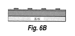
図6A-6Eは、図5に示した方法による太陽電池装置の製造の中間状態を示す。図6Aは、基板601と、単一または多数のセルユニット603と、酸化されていない窓層605と、キャップ層607とを含む出発エピタキシャル材料を示す。通常の技能を備えた当業者であれば、任意の数のセルユニットまたは接合を本願の太陽電池装置において使用できることは理解するはずである。酸化されていない窓層は、AlGaAs、AlAs、InAlAs、またはInAlPなどのAl含有III-V族化合物半導体物質を含むことができる。このキャップ層は、太陽電池装置の正面すなわち上面のグリッド金属接点との電気的接触を高めることができる。
6A-6E show an intermediate state of manufacturing the solar cell device by the method shown in FIG. FIG. 6A shows a starting epitaxial material that includes a
図6Bは、キャップ層607がグリッド金属接点613のパターンに従ってエッチングされている状態を示す。キャップ層をエッチングした後、窓層605を酸化するためウェハは図2Bで示したように炉内に装填される。図6Cは、キャップ層の除去部分に対応する窓層605の露出部分が酸化されて、酸化された窓層609を形成している状態を示す。酸化処理の後、ウェハは炉から取り出され、残ったキャップ層の上にグリッド金属接点が形成される。図6Dは、グリッド金属接点613がキャップ層の上に形成されていることを示す。さらに、図6Dは、反射防止コーティング611が酸化された窓層609層の表面上に形成されていることも示している。図6Eは、絶縁エッチングが施され、裏面金属接点615が太陽電池装置に設けられていることを示す。
FIG. 6B shows the
実験目的で、2500オングストロームのInAlP窓層を備えた標準的なInGaP/GaAs二重接合太陽電池装置からなる太陽電池構造体を成長させる。上部接点層はパターン化され且つエッチングされ、ウェハは幾つかの数片に切断する。二片は高温の湿式酸化処理により酸化する。これら二片の一方では、窓層は完全に酸化させる。残りの一片では、窓層の上半分のみを酸化させる。三番目の片は酸化させないままにする。次に、これら三片すべては処理して太陽電池装置とし、光ルネッセンス(PL)、電流-電圧(IV)データ、及び内部量子効率(IQE)を測定するためテストした。 For experimental purposes, a solar cell structure consisting of a standard InGaP / GaAs double junction solar cell device with a 2500 Å InAlP window layer is grown. The top contact layer is patterned and etched and the wafer is cut into several pieces. The two pieces are oxidized by a high temperature wet oxidation process. In one of these two pieces, the window layer is completely oxidized. The remaining piece oxidizes only the upper half of the window layer. Leave the third piece unoxidized. All three pieces were then processed into solar cell devices and tested to measure optical luminescence (PL), current-voltage (IV) data, and internal quantum efficiency (IQE).
図7は、これら3つの試料のPLを測定したテストの結果を示す。すなわち、このグラフは、酸化されていないInAlP窓層、部分的に酸化されたInAlP窓層、及び完全に酸化されたInAlP窓層を備えた上部InGaPセルユニットのPLを示す。酸化された窓層で終端する上部InGaPセルユニットのPLは、酸化されていない窓層で終端する上部InGaPセルユニットのPLより大幅に強いことが示されている。このテスト結果は、酸化された窓層が再結合によるキャリア損失を減少させ、この酸化物が太陽電池装置の表面を不動態化することを示している。さらに、酸化された窓層で終端する上部InGaPセルユニットのPLは、酸化されていない窓層で終端する上部InGaPセルユニットのPLより僅かに青方偏移している。このテスト結果は、酸化された窓層が、窓層による太陽スペクトルの遠青端の吸収を減少させることを示している。 FIG. 7 shows the test results of measuring the PL of these three samples. That is, this graph shows the PL of the upper InGaP cell unit with an unoxidized InAlP window layer, a partially oxidized InAlP window layer, and a fully oxidized InAlP window layer. It has been shown that the PL of the upper InGaP cell unit terminating in the oxidized window layer is significantly stronger than the PL of the upper InGaP cell unit terminating in the non-oxidized window layer. The test results show that the oxidized window layer reduces the carrier loss due to recombination and the oxide passivates the surface of the solar cell device. Furthermore, the PL of the upper InGaP cell unit that terminates in the oxidized window layer is slightly blue shifted from the PL of the upper InGaP cell unit that terminates in the non-oxidized window layer. This test result shows that the oxidized window layer reduces the absorption of the far blue end of the solar spectrum by the window layer.
図8は、酸化されていない二重接合太陽電池装置、半分酸化された二重接合太陽電池装置、及び完全に酸化された二重接合太陽電池装置のIVデータを測定したテストの結果を示す。測定はAM-1.5照明の下で行われる。酸化された二重接合太陽電池装置ではより高い短絡電流(Isc)が得られた。この結果は、窓層の透明度が増加したために、付加的な光子が上部InGaPセルユニットに到達したことを示している。 FIG. 8 shows the results of a test measuring IV data for a non-oxidized double junction solar cell device, a half-oxidized double junction solar cell device, and a fully oxidized double junction solar cell device. Measurements are made under AM-1.5 illumination. Higher short circuit current (Isc) was obtained in the oxidized double junction solar cell device. This result indicates that additional photons have reached the upper InGaP cell unit due to the increased transparency of the window layer.
図9は、酸化されていない二重接合太陽電池装置、半分酸化された二重接合太陽電池装置、及び完全に酸化された二重接合太陽電池装置のIQE測定値を示す。IQEは、セルから反射または透過されない光子が収集可能な電流を発生できる効率を示す。これら3つの二重接合太陽電池装置のIQEは、スペクトルの遠青端を除けば似ている。酸化された試料に関しては、InAlP窓層により吸収される(そして無駄になる)光子が少ないので、付加的な効率が得られる。スペクトルの遠青端において酸化されたセルの応答が増加しているのは、酸化処理の結果としてInAlP窓層の透明度が増加しているからである。 FIG. 9 shows IQE measurements for a non-oxidized double junction solar cell device, a half-oxidized double junction solar cell device, and a fully oxidized double junction solar cell device. IQE indicates the efficiency with which photons that are not reflected or transmitted from the cell can generate a collectable current. The IQE of these three double junction solar cell devices is similar except for the far blue end of the spectrum. For oxidized samples, additional efficiency is obtained because fewer photons are absorbed (and wasted) by the InAlP window layer. The increased response of the oxidized cell at the far blue end of the spectrum is due to the increased transparency of the InAlP window layer as a result of the oxidation treatment.
本願の利点の1つは、III-V族化合物半導体の太陽電池装置の効率が、酸化された窓層を用いることで大幅に向上していることである。酸化された窓層は酸化されていない窓層より広いバンドギャップを持っており、酸化された窓層はより多くの光を太陽電池装置のセルユニットに伝達できる。酸化された窓層のより広いバンドギャップがホールと電子の表面再結合を減少させ、従って、太陽電池装置の効率を向上させる。 One of the advantages of the present application is that the efficiency of a III-V compound semiconductor solar cell device is greatly improved by using an oxidized window layer. The oxidized window layer has a wider band gap than the non-oxidized window layer, and the oxidized window layer can transmit more light to the cell unit of the solar cell device. The wider band gap of the oxidized window layer reduces the surface recombination of holes and electrons, thus improving the efficiency of the solar cell device.
上述の利点は、窓層が酸化された太陽電池装置の製造過程に関わる複雑さを上回る。窓層を酸化させるには、ウェハを太陽電池装置の製造工程において炉に装填し、炉から取り出す。製造工程は複雑になるが、本願は、酸化された窓層により広いバンドギャップをもたらし、且つ太陽スペクトルの遠青端すなわち紫外線領域における酸化された窓層の光学的透明度を向上させる。 The above advantages outweigh the complexity involved in the process of manufacturing a solar cell device with an oxidized window layer. To oxidize the window layer, the wafer is loaded into the furnace and removed from the furnace in the manufacturing process of the solar cell device. Although the manufacturing process is complicated, the present application provides a wider band gap with the oxidized window layer and improves the optical transparency of the oxidized window layer at the far blue end of the solar spectrum, ie, in the ultraviolet region.
本願の多くの修正及び代替的な実施形態は、上述の記載を考慮すれば通常の技能を備えた当業者には明白となるはずである。従って、この記載は、例示的なものとしてのみ解釈されるべきであり、また、これは通常の技能を備えた当業者に本願を実施するための最良の様態を教示するためのものである。上述の構成の詳細は、本願の精神から逸脱することなく実質的に変更することができ、添付した特許請求の範囲内に入る全ての修正の排他的使用権は、保持されている。本願は、添付の特許請求の範囲及び適用法規が要求する範囲においてのみ限定されることが意図されている。 Many modifications and alternative embodiments of the present application should be apparent to those of ordinary skill in the art in view of the above description. Accordingly, this description is to be construed as illustrative only and is for the purpose of teaching those skilled in the art the best mode of carrying out the invention with ordinary skill. The details of the construction described above may vary substantially without departing from the spirit of the present application, and the exclusive use rights of all modifications falling within the scope of the appended claims are retained. This application is intended to be limited only to the extent required by the appended claims and applicable law.
更に、以下の特許請求の範囲は、ここに説明された本発明の全ての一般的特徴と具体的特徴とを網羅するものであり、また本発明の範囲に関する全ての言明をも網羅する。 Furthermore, the following claims are intended to cover all general and specific features of the invention described herein, as well as all statements regarding the scope of the invention.
Claims (28)
太陽スペクトルの所定の波長を吸収するよう構成された少なくとも1つのセルユニットを、III-V族化合物半導体物質から形成する段階と、
前記太陽電池装置の上面における光発生キャリアの再結合を防止するために窓層を前記セルユニットの上に形成する段階と、
前記窓層を酸化された窓層に転換するため前記窓層を酸化させる段階とを含む、方法。 A method for producing a group III-V compound semiconductor solar cell device comprising:
Forming at least one cell unit configured to absorb a predetermined wavelength of the solar spectrum from a III-V compound semiconductor material;
Forming a window layer on the cell unit to prevent recombination of photogenerated carriers on the top surface of the solar cell device;
Oxidizing the window layer to convert the window layer to an oxidized window layer.
金属導電物質との電気的接触を向上させるために前記窓層の上にキャップ層を設ける段階と、
前記キャップ層をエッチングする段階と、
前記窓層の露出部分を酸化する段階とを含み、前記露出部分は前記キャップ層のエッチングされた部分に対応する、請求項11に記載の方法。 Said step of oxidizing,
Providing a cap layer on the window layer to improve electrical contact with the metal conductive material;
Etching the cap layer;
12. The method of claim 11, comprising oxidizing an exposed portion of the window layer, the exposed portion corresponding to an etched portion of the cap layer.
反射防止コーティングを前記酸化された窓層に施す段階とをさらに含む、請求項12に記載の方法。 Providing the metal conductive material on the cap layer;
13. The method of claim 12, further comprising applying an anti-reflective coating to the oxidized window layer.
前記窓層を、その選択した部分を酸化させるのに十分な温度で且つ十分な時間にわたって湿った環境に暴露する段階を含む請求項1に記載の方法。 The step of oxidizing the window layer comprises:
The method of claim 1, comprising exposing the window layer to a moist environment at a temperature sufficient to oxidize selected portions of the window layer for a sufficient time.
III-V族化合物半導体物質から形成されると共に、太陽スペクトルの所定の波長を吸収するよう構成された少なくとも1つのセルユニットと、
前記太陽電池装置の上面における光発生キャリアの再結合を防止するために前記セルユニットの上に設けられた酸化された窓層とを含む、太陽電池装置。 A solar cell device,
At least one cell unit formed from a III-V compound semiconductor material and configured to absorb a predetermined wavelength of the solar spectrum;
A solar cell device comprising an oxidized window layer provided on the cell unit to prevent recombination of photogenerated carriers on the upper surface of the solar cell device.
As)と、りん化インジウム(InP)と、ひ化りん化インジウムガリウム(Ga1-xInxAs1-yPy)と、アルミニウムインジウムガリウムリン((AlxGa1-x)1-yInyP)とのうち任意のものから形成される、請求項19に記載の太陽電池装置。 The cell unit includes gallium arsenide (GaAs), gallium indium phosphide (Ga 1-x In x P), and gallium indium arsenide (Ga 1-x In x
As), indium phosphide (InP), indium gallium arsenide phosphide (Ga 1-x In x As 1-y P y ), and aluminum indium gallium phosphide ((Al x Ga 1-x ) 1-y 20. The solar cell device according to claim 19, wherein the solar cell device is formed of any one of In y P).
Applications Claiming Priority (3)
| Application Number | Priority Date | Filing Date | Title |
|---|---|---|---|
| US14792909P | 2009-01-28 | 2009-01-28 | |
| US61/147,929 | 2009-01-28 | ||
| PCT/US2010/022385 WO2010088370A1 (en) | 2009-01-28 | 2010-01-28 | High efficiency group iii-v compound semiconductor solar cell with oxidized window layer |
Publications (1)
| Publication Number | Publication Date |
|---|---|
| JP2012516578A true JP2012516578A (en) | 2012-07-19 |
Family
ID=42353181
Family Applications (1)
| Application Number | Title | Priority Date | Filing Date |
|---|---|---|---|
| JP2011548289A Pending JP2012516578A (en) | 2009-01-28 | 2010-01-28 | High-efficiency III-V compound semiconductor solar cell device with oxidation window layer |
Country Status (7)
| Country | Link |
|---|---|
| US (2) | US9356162B2 (en) |
| EP (1) | EP2392030B1 (en) |
| JP (1) | JP2012516578A (en) |
| AU (1) | AU2010208225B2 (en) |
| CA (1) | CA2750656C (en) |
| IL (1) | IL214311A (en) |
| WO (1) | WO2010088370A1 (en) |
Cited By (3)
| Publication number | Priority date | Publication date | Assignee | Title |
|---|---|---|---|---|
| EP2966692A1 (en) | 2014-07-11 | 2016-01-13 | Ricoh Company, Ltd. | Compound-semiconductor photovoltaic cell and manufacturing method of compound-semiconductor photovoltaic cell |
| US9243179B2 (en) | 2013-02-18 | 2016-01-26 | Ricoh Company, Ltd. | Reaction material and chemical heat pump |
| JP2023171911A (en) * | 2018-10-24 | 2023-12-05 | ファースト・ソーラー・インコーポレーテッド | Buffer layer for photovoltaic devices with group V doping |
Families Citing this family (22)
| Publication number | Priority date | Publication date | Assignee | Title |
|---|---|---|---|---|
| FR2894990B1 (en) | 2005-12-21 | 2008-02-22 | Soitec Silicon On Insulator | PROCESS FOR PRODUCING SUBSTRATES, IN PARTICULAR FOR OPTICS, ELECTRONICS OR OPTOELECTRONICS AND SUBSTRATE OBTAINED BY SAID PROCESS |
| US10000965B2 (en) | 2010-01-16 | 2018-06-19 | Cardinal Cg Company | Insulating glass unit transparent conductive coating technology |
| US10060180B2 (en) | 2010-01-16 | 2018-08-28 | Cardinal Cg Company | Flash-treated indium tin oxide coatings, production methods, and insulating glass unit transparent conductive coating technology |
| US10000411B2 (en) | 2010-01-16 | 2018-06-19 | Cardinal Cg Company | Insulating glass unit transparent conductivity and low emissivity coating technology |
| US8852994B2 (en) | 2010-05-24 | 2014-10-07 | Masimo Semiconductor, Inc. | Method of fabricating bifacial tandem solar cells |
| RU2436194C1 (en) * | 2010-08-31 | 2011-12-10 | Учреждение Российской академии наук Физико-технический институт им. А.Ф. Иоффе РАН | Method for producing chips of concentrator solar photocells |
| US8455290B2 (en) * | 2010-09-04 | 2013-06-04 | Masimo Semiconductor, Inc. | Method of fabricating epitaxial structures |
| FR2981195B1 (en) | 2011-10-11 | 2024-08-23 | Soitec Silicon On Insulator | MULTI-JUNCTIONS IN A SEMICONDUCTOR DEVICE FORMED BY DIFFERENT DEPOSITION TECHNIQUES |
| US9136402B2 (en) * | 2012-02-28 | 2015-09-15 | International Business Machines Corporation | High efficiency flexible solar cells for consumer electronics |
| RU2493634C1 (en) * | 2012-04-04 | 2013-09-20 | Федеральное государственное бюджетное учреждение науки Физико-технический институт им. А.Ф. Иоффе Российской академии наук | Method of making multistage photocell chips |
| US9853180B2 (en) * | 2013-06-19 | 2017-12-26 | Solaero Technologies Corp. | Inverted metamorphic multijunction solar cell with surface passivation |
| US20140373906A1 (en) * | 2013-06-25 | 2014-12-25 | Solar Junction Corporation | Anti-reflection coatings for multijunction solar cells |
| US20150034151A1 (en) * | 2013-07-30 | 2015-02-05 | Emcore Solar Power, Inc. | Inverted metamorphic multijunction solar cell with passivation in the window layer |
| US20150034152A1 (en) * | 2013-07-30 | 2015-02-05 | Emcore Solar Power, Inc. | Solar cell with passivation on the window layer |
| US20150059837A1 (en) * | 2013-08-30 | 2015-03-05 | Emcore Solar Power, Inc. | Solar cell with passivation on the contact layer |
| WO2015084810A2 (en) | 2013-12-05 | 2015-06-11 | The Board Of Regents Of The University Of Oklahoma | Thermophotovoltaic materials, methods of deposition, and devices |
| RU2647979C1 (en) * | 2016-11-17 | 2018-03-21 | Общество с ограниченной ответственностью "ИоффеЛЕД" | Method of producing diodes of medium-wave infrared spectrum |
| US11028012B2 (en) | 2018-10-31 | 2021-06-08 | Cardinal Cg Company | Low solar heat gain coatings, laminated glass assemblies, and methods of producing same |
| US10916678B2 (en) * | 2019-04-16 | 2021-02-09 | National Central University | Method of substrate lift-off for high-efficiency group III-V solar cell for reuse |
| US11784272B2 (en) * | 2021-04-29 | 2023-10-10 | Solaero Technologies Corp. | Multijunction solar cell |
| EP4231362A1 (en) * | 2022-02-21 | 2023-08-23 | SolAero Technologies Corp., a corporation of the state of Delaware | Multijunction solar cell |
| CN115064606B (en) * | 2022-06-16 | 2024-09-03 | 湖南红太阳光电科技有限公司 | Water vapor annealing process for improving passivation effect of polycrystalline silicon layer |
Citations (11)
| Publication number | Priority date | Publication date | Assignee | Title |
|---|---|---|---|---|
| JPS5618474A (en) * | 1979-07-23 | 1981-02-21 | Ibm | Semiconducotr solar battery |
| JPH05304147A (en) * | 1992-04-27 | 1993-11-16 | Fujitsu Ltd | Method for manufacturing semiconductor device |
| JPH06503919A (en) * | 1990-12-31 | 1994-04-28 | ザ ボード オブ トラスティース オブ ザ ユニバーシティ オブ イリノイ | AlGaAs natural oxide |
| JPH11330531A (en) * | 1998-05-18 | 1999-11-30 | Furukawa Electric Co Ltd:The | Semiconductor light receiving element and method of manufacturing the same |
| JP2001237500A (en) * | 1999-12-15 | 2001-08-31 | Matsushita Electric Ind Co Ltd | Semiconductor light emitting device and method of manufacturing the same |
| JP2004296658A (en) * | 2003-03-26 | 2004-10-21 | Sharp Corp | Multijunction solar cell and current matching method thereof |
| JP2005512306A (en) * | 2001-07-27 | 2005-04-28 | エムコア・コーポレイション | Solar cell device having bypass diode for reverse bias protection and method for manufacturing the same |
| JP2006013531A (en) * | 1998-05-28 | 2006-01-12 | Emcore Corp | Solar cell with bypass diode |
| JP2006073749A (en) * | 2004-09-01 | 2006-03-16 | Ishikawajima Harima Heavy Ind Co Ltd | Manufacturing method of semiconductor device |
| JP2007504659A (en) * | 2003-09-05 | 2007-03-01 | 新科實業有限公司 | Systems and methods having metal-semiconductor-metal (MSM) photodetectors with buried oxide layers |
| JP2007335753A (en) * | 2006-06-16 | 2007-12-27 | Sumitomo Electric Ind Ltd | Semiconductor light receiving element, manufacturing method thereof, and light receiving device |
Family Cites Families (6)
| Publication number | Priority date | Publication date | Assignee | Title |
|---|---|---|---|---|
| US4107723A (en) * | 1977-05-02 | 1978-08-15 | Hughes Aircraft Company | High bandgap window layer for GaAs solar cells and fabrication process therefor |
| US4575577A (en) * | 1983-05-27 | 1986-03-11 | Chevron Research Company | Ternary III-V multicolor solar cells containing a quaternary window layer and a quaternary transition layer |
| US5262360A (en) * | 1990-12-31 | 1993-11-16 | The Board Of Trustees Of The University Of Illinois | AlGaAs native oxide |
| US5330585A (en) * | 1992-10-30 | 1994-07-19 | Spectrolab, Inc. | Gallium arsenide/aluminum gallium arsenide photocell including environmentally sealed ohmic contact grid interface and method of fabricating the cell |
| US7812249B2 (en) * | 2003-04-14 | 2010-10-12 | The Boeing Company | Multijunction photovoltaic cell grown on high-miscut-angle substrate |
| GB0719554D0 (en) | 2007-10-05 | 2007-11-14 | Univ Glasgow | semiconductor optoelectronic devices and methods for making semiconductor optoelectronic devices |
-
2010
- 2010-01-28 JP JP2011548289A patent/JP2012516578A/en active Pending
- 2010-01-28 US US12/695,671 patent/US9356162B2/en active Active
- 2010-01-28 CA CA2750656A patent/CA2750656C/en active Active
- 2010-01-28 AU AU2010208225A patent/AU2010208225B2/en active Active
- 2010-01-28 EP EP10736391.3A patent/EP2392030B1/en active Active
- 2010-01-28 WO PCT/US2010/022385 patent/WO2010088370A1/en not_active Ceased
-
2011
- 2011-07-27 IL IL214311A patent/IL214311A/en active IP Right Grant
-
2012
- 2012-05-29 US US13/482,716 patent/US20120227798A1/en not_active Abandoned
Patent Citations (11)
| Publication number | Priority date | Publication date | Assignee | Title |
|---|---|---|---|---|
| JPS5618474A (en) * | 1979-07-23 | 1981-02-21 | Ibm | Semiconducotr solar battery |
| JPH06503919A (en) * | 1990-12-31 | 1994-04-28 | ザ ボード オブ トラスティース オブ ザ ユニバーシティ オブ イリノイ | AlGaAs natural oxide |
| JPH05304147A (en) * | 1992-04-27 | 1993-11-16 | Fujitsu Ltd | Method for manufacturing semiconductor device |
| JPH11330531A (en) * | 1998-05-18 | 1999-11-30 | Furukawa Electric Co Ltd:The | Semiconductor light receiving element and method of manufacturing the same |
| JP2006013531A (en) * | 1998-05-28 | 2006-01-12 | Emcore Corp | Solar cell with bypass diode |
| JP2001237500A (en) * | 1999-12-15 | 2001-08-31 | Matsushita Electric Ind Co Ltd | Semiconductor light emitting device and method of manufacturing the same |
| JP2005512306A (en) * | 2001-07-27 | 2005-04-28 | エムコア・コーポレイション | Solar cell device having bypass diode for reverse bias protection and method for manufacturing the same |
| JP2004296658A (en) * | 2003-03-26 | 2004-10-21 | Sharp Corp | Multijunction solar cell and current matching method thereof |
| JP2007504659A (en) * | 2003-09-05 | 2007-03-01 | 新科實業有限公司 | Systems and methods having metal-semiconductor-metal (MSM) photodetectors with buried oxide layers |
| JP2006073749A (en) * | 2004-09-01 | 2006-03-16 | Ishikawajima Harima Heavy Ind Co Ltd | Manufacturing method of semiconductor device |
| JP2007335753A (en) * | 2006-06-16 | 2007-12-27 | Sumitomo Electric Ind Ltd | Semiconductor light receiving element, manufacturing method thereof, and light receiving device |
Cited By (4)
| Publication number | Priority date | Publication date | Assignee | Title |
|---|---|---|---|---|
| US9243179B2 (en) | 2013-02-18 | 2016-01-26 | Ricoh Company, Ltd. | Reaction material and chemical heat pump |
| EP2966692A1 (en) | 2014-07-11 | 2016-01-13 | Ricoh Company, Ltd. | Compound-semiconductor photovoltaic cell and manufacturing method of compound-semiconductor photovoltaic cell |
| JP2023171911A (en) * | 2018-10-24 | 2023-12-05 | ファースト・ソーラー・インコーポレーテッド | Buffer layer for photovoltaic devices with group V doping |
| JP7667219B2 (en) | 2018-10-24 | 2025-04-22 | ファースト・ソーラー・インコーポレーテッド | Buffer layer for photovoltaic devices having group V doping - Patents.com |
Also Published As
| Publication number | Publication date |
|---|---|
| EP2392030B1 (en) | 2020-04-15 |
| IL214311A0 (en) | 2011-09-27 |
| EP2392030A4 (en) | 2013-10-30 |
| AU2010208225A1 (en) | 2011-08-18 |
| CA2750656A1 (en) | 2010-08-05 |
| IL214311A (en) | 2017-04-30 |
| AU2010208225B2 (en) | 2015-11-05 |
| US9356162B2 (en) | 2016-05-31 |
| WO2010088370A1 (en) | 2010-08-05 |
| US20120227798A1 (en) | 2012-09-13 |
| EP2392030A1 (en) | 2011-12-07 |
| CA2750656C (en) | 2016-08-23 |
| US20100186822A1 (en) | 2010-07-29 |
Similar Documents
| Publication | Publication Date | Title |
|---|---|---|
| US9356162B2 (en) | High efficiency group III-V compound semiconductor solar cell with oxidized window layer | |
| CN104091849B (en) | Multi-junction solar cell and manufacturing method thereof | |
| TWI594449B (en) | Four-contact reverse metamorphic multi-contact solar cell with two metamorphic layers | |
| US20100218819A1 (en) | Semiconductor optoelectronic devices and methods for making semiconductor optoelectronic devices | |
| KR101957801B1 (en) | Flexible Double Junction Solar Cell Device | |
| US20130228216A1 (en) | Solar cell with gradation in doping in the window layer | |
| Hsu et al. | The analysis of dual-junction tandem solar cells enhanced by surface dispensed quantum dots | |
| TWI647736B (en) | Dilute nitride devices with active group iv substrate and controlled dopant diffusion at the nucleation layer-substrate interface | |
| CN101304051B (en) | Solar cells with graded superlattice structure | |
| Steiner et al. | Reverse heterojunction (Al) GaInP solar cells for improved efficiency at concentration | |
| Gupta et al. | Design and fabrication of a photodetector for UV/Blue wavelength region for low-light intensity levels using InGaN/GaN superlattice structure | |
| US20120216857A1 (en) | Solar Cell Assembly with an Improved Photocurrent Collection Efficiency | |
| US11171253B2 (en) | Solar cell, multi-junction solar cell, solar cell module, and photovoltaic system | |
| US20150034152A1 (en) | Solar cell with passivation on the window layer | |
| JP5283588B2 (en) | Solar cell | |
| US10910506B1 (en) | Solar cell with gradation in the top window layer | |
| Ataser et al. | Developing of dual junction GaInP/GaAs solar cell devices: effects of different metal contacts | |
| Chen et al. | Natural lithography nano-sphere texturing as antireflective layer on InP-based pin photodiodes | |
| CN110335904B (en) | An InGaN/GaN Multiple Quantum Well Solar Cell Inserted with AlInGaN Barrier Layer Structure | |
| Fan et al. | Epitaxial GaAsP/Si tandem solar cells with integrated light trapping | |
| Forghani et al. | MOVPE growth of AlInP-InGaP distributed Bragg reflectors (DBR) for monolithic integration into multijunction solar cells | |
| US20150059837A1 (en) | Solar cell with passivation on the contact layer | |
| Cai et al. | Dependence of the property of InGaN pin solar cells on the light concentration and temperature | |
| Behaghel et al. | Four-fold MQWs absorption enhancement in a 430 nm thick InGaAs/GaAsP MQWs solar cell | |
| Liu et al. | Performance improvement of triple-junctions GaAs-based solar cell using SiO 2-nanopillars/SiO 2/TiO 2 graded-index anti-reflection coating |
Legal Events
| Date | Code | Title | Description |
|---|---|---|---|
| A977 | Report on retrieval |
Free format text: JAPANESE INTERMEDIATE CODE: A971007 Effective date: 20130212 |
|
| A131 | Notification of reasons for refusal |
Free format text: JAPANESE INTERMEDIATE CODE: A131 Effective date: 20130319 |
|
| A601 | Written request for extension of time |
Free format text: JAPANESE INTERMEDIATE CODE: A601 Effective date: 20130619 |
|
| A602 | Written permission of extension of time |
Free format text: JAPANESE INTERMEDIATE CODE: A602 Effective date: 20130626 |
|
| A601 | Written request for extension of time |
Free format text: JAPANESE INTERMEDIATE CODE: A601 Effective date: 20130719 |
|
| A521 | Request for written amendment filed |
Free format text: JAPANESE INTERMEDIATE CODE: A523 Effective date: 20130726 |
|
| A602 | Written permission of extension of time |
Free format text: JAPANESE INTERMEDIATE CODE: A602 Effective date: 20130726 |
|
| A131 | Notification of reasons for refusal |
Free format text: JAPANESE INTERMEDIATE CODE: A131 Effective date: 20130903 |
|
| A601 | Written request for extension of time |
Free format text: JAPANESE INTERMEDIATE CODE: A601 Effective date: 20131203 |
|
| A602 | Written permission of extension of time |
Free format text: JAPANESE INTERMEDIATE CODE: A602 Effective date: 20131210 |
|
| A521 | Request for written amendment filed |
Free format text: JAPANESE INTERMEDIATE CODE: A523 Effective date: 20140303 |
|
| A02 | Decision of refusal |
Free format text: JAPANESE INTERMEDIATE CODE: A02 Effective date: 20140404 |