JP2012164686A - Optical sensor and display device - Google Patents
Optical sensor and display device Download PDFInfo
- Publication number
- JP2012164686A JP2012164686A JP2009143298A JP2009143298A JP2012164686A JP 2012164686 A JP2012164686 A JP 2012164686A JP 2009143298 A JP2009143298 A JP 2009143298A JP 2009143298 A JP2009143298 A JP 2009143298A JP 2012164686 A JP2012164686 A JP 2012164686A
- Authority
- JP
- Japan
- Prior art keywords
- transistor
- storage node
- wiring
- optical sensor
- control electrode
- Prior art date
- Legal status (The legal status is an assumption and is not a legal conclusion. Google has not performed a legal analysis and makes no representation as to the accuracy of the status listed.)
- Withdrawn
Links
Images





Classifications
-
- G—PHYSICS
- G06—COMPUTING OR CALCULATING; COUNTING
- G06F—ELECTRIC DIGITAL DATA PROCESSING
- G06F3/00—Input arrangements for transferring data to be processed into a form capable of being handled by the computer; Output arrangements for transferring data from processing unit to output unit, e.g. interface arrangements
- G06F3/01—Input arrangements or combined input and output arrangements for interaction between user and computer
- G06F3/03—Arrangements for converting the position or the displacement of a member into a coded form
- G06F3/041—Digitisers, e.g. for touch screens or touch pads, characterised by the transducing means
- G06F3/0412—Digitisers structurally integrated in a display
-
- G—PHYSICS
- G06—COMPUTING OR CALCULATING; COUNTING
- G06F—ELECTRIC DIGITAL DATA PROCESSING
- G06F3/00—Input arrangements for transferring data to be processed into a form capable of being handled by the computer; Output arrangements for transferring data from processing unit to output unit, e.g. interface arrangements
- G06F3/01—Input arrangements or combined input and output arrangements for interaction between user and computer
- G06F3/03—Arrangements for converting the position or the displacement of a member into a coded form
- G06F3/041—Digitisers, e.g. for touch screens or touch pads, characterised by the transducing means
- G06F3/042—Digitisers, e.g. for touch screens or touch pads, characterised by the transducing means by opto-electronic means
-
- G—PHYSICS
- G02—OPTICS
- G02F—OPTICAL DEVICES OR ARRANGEMENTS FOR THE CONTROL OF LIGHT BY MODIFICATION OF THE OPTICAL PROPERTIES OF THE MEDIA OF THE ELEMENTS INVOLVED THEREIN; NON-LINEAR OPTICS; FREQUENCY-CHANGING OF LIGHT; OPTICAL LOGIC ELEMENTS; OPTICAL ANALOGUE/DIGITAL CONVERTERS
- G02F1/00—Devices or arrangements for the control of the intensity, colour, phase, polarisation or direction of light arriving from an independent light source, e.g. switching, gating or modulating; Non-linear optics
- G02F1/01—Devices or arrangements for the control of the intensity, colour, phase, polarisation or direction of light arriving from an independent light source, e.g. switching, gating or modulating; Non-linear optics for the control of the intensity, phase, polarisation or colour
- G02F1/13—Devices or arrangements for the control of the intensity, colour, phase, polarisation or direction of light arriving from an independent light source, e.g. switching, gating or modulating; Non-linear optics for the control of the intensity, phase, polarisation or colour based on liquid crystals, e.g. single liquid crystal display cells
- G02F1/133—Constructional arrangements; Operation of liquid crystal cells; Circuit arrangements
- G02F1/13306—Circuit arrangements or driving methods for the control of single liquid crystal cells
- G02F1/13318—Circuits comprising a photodetector
-
- G—PHYSICS
- G02—OPTICS
- G02F—OPTICAL DEVICES OR ARRANGEMENTS FOR THE CONTROL OF LIGHT BY MODIFICATION OF THE OPTICAL PROPERTIES OF THE MEDIA OF THE ELEMENTS INVOLVED THEREIN; NON-LINEAR OPTICS; FREQUENCY-CHANGING OF LIGHT; OPTICAL LOGIC ELEMENTS; OPTICAL ANALOGUE/DIGITAL CONVERTERS
- G02F2203/00—Function characteristic
- G02F2203/60—Temperature independent
-
- G—PHYSICS
- G09—EDUCATION; CRYPTOGRAPHY; DISPLAY; ADVERTISING; SEALS
- G09G—ARRANGEMENTS OR CIRCUITS FOR CONTROL OF INDICATING DEVICES USING STATIC MEANS TO PRESENT VARIABLE INFORMATION
- G09G2320/00—Control of display operating conditions
- G09G2320/04—Maintaining the quality of display appearance
- G09G2320/041—Temperature compensation
-
- G—PHYSICS
- G09—EDUCATION; CRYPTOGRAPHY; DISPLAY; ADVERTISING; SEALS
- G09G—ARRANGEMENTS OR CIRCUITS FOR CONTROL OF INDICATING DEVICES USING STATIC MEANS TO PRESENT VARIABLE INFORMATION
- G09G2360/00—Aspects of the architecture of display systems
- G09G2360/14—Detecting light within display terminals, e.g. using a single or a plurality of photosensors
- G09G2360/144—Detecting light within display terminals, e.g. using a single or a plurality of photosensors the light being ambient light
-
- G—PHYSICS
- G09—EDUCATION; CRYPTOGRAPHY; DISPLAY; ADVERTISING; SEALS
- G09G—ARRANGEMENTS OR CIRCUITS FOR CONTROL OF INDICATING DEVICES USING STATIC MEANS TO PRESENT VARIABLE INFORMATION
- G09G3/00—Control arrangements or circuits, of interest only in connection with visual indicators other than cathode-ray tubes
- G09G3/20—Control arrangements or circuits, of interest only in connection with visual indicators other than cathode-ray tubes for presentation of an assembly of a number of characters, e.g. a page, by composing the assembly by combination of individual elements arranged in a matrix no fixed position being assigned to or needed to be assigned to the individual characters or partial characters
- G09G3/34—Control arrangements or circuits, of interest only in connection with visual indicators other than cathode-ray tubes for presentation of an assembly of a number of characters, e.g. a page, by composing the assembly by combination of individual elements arranged in a matrix no fixed position being assigned to or needed to be assigned to the individual characters or partial characters by control of light from an independent source
- G09G3/36—Control arrangements or circuits, of interest only in connection with visual indicators other than cathode-ray tubes for presentation of an assembly of a number of characters, e.g. a page, by composing the assembly by combination of individual elements arranged in a matrix no fixed position being assigned to or needed to be assigned to the individual characters or partial characters by control of light from an independent source using liquid crystals
- G09G3/3611—Control of matrices with row and column drivers
- G09G3/3648—Control of matrices with row and column drivers using an active matrix
Landscapes
- Engineering & Computer Science (AREA)
- General Engineering & Computer Science (AREA)
- Theoretical Computer Science (AREA)
- Human Computer Interaction (AREA)
- Physics & Mathematics (AREA)
- General Physics & Mathematics (AREA)
- Liquid Crystal (AREA)
- Transforming Light Signals Into Electric Signals (AREA)
- Solid State Image Pick-Up Elements (AREA)
- Control Of Indicators Other Than Cathode Ray Tubes (AREA)
- Devices For Indicating Variable Information By Combining Individual Elements (AREA)
- Light Receiving Elements (AREA)
- Liquid Crystal Display Device Control (AREA)
Abstract
【課題】ダイナミックレンジが広く、かつ温度依存性が低減された光センサおよび、この光センサを用いた表示装置を提供する。
【解決手段】光センサは、蓄積ノードと、リセット信号配線と、読み出し信号配線と、光検出用素子と、遮光層を有する参照用素子と、リセット信号が供給されてから読み出し信号が供給されるまでのセンシング期間に、光検出素子を流れる光量に応じた電流および参照用素子に流れる電流に応じて変化した蓄積ノードの電位を、読み出し信号にしたがって読み出し出力する、第1のスイッチング素子と、蓄積ノードと参照用素子との間に設けられ、読み出し信号供給時に蓄積ノードの電位が参照用素子の蓄積ノードとは反対側の電位より高くなった場合に、蓄積ノードと参照用素子との間を非導通状態にする第2のスイッチング素子とを備える。
【選択図】図1An optical sensor having a wide dynamic range and reduced temperature dependence, and a display device using the optical sensor are provided.
An optical sensor is supplied with a read signal after a storage node, a reset signal line, a read signal line, a light detection element, a reference element having a light shielding layer, and a reset signal are supplied. A first switching element that reads out and outputs a current corresponding to the amount of light flowing through the light detection element and a potential of the storage node that changes according to the current flowing through the reference element during the sensing period until Provided between the storage node and the reference element, when the potential of the storage node becomes higher than the potential of the reference element opposite to the storage node when the read signal is supplied. And a second switching element that is brought into a non-conduction state.
[Selection] Figure 1
Description
本発明は、フォトダイオード等の光検出素子を有する光センサおよび、この光センサを画素領域内に備えた表示装置に関する。 The present invention relates to a photosensor having a photodetection element such as a photodiode, and a display device including the photosensor in a pixel region.
従来、例えばフォトダイオード等の光検出素子を画素内に備えたことにより、外光の明るさを検出したり、ディスプレイに近接した物体の画像を取り込んだりすることが可能な、光センサ付き表示装置が提案されている。このような光センサ付き表示装置は、双方向通信用表示装置や、タッチパネル機能付き表示装置としての利用が想定されている。 Conventionally, a display device with a photosensor that can detect the brightness of external light or capture an image of an object close to the display by providing a photodetection element such as a photodiode in the pixel. Has been proposed. Such a display device with an optical sensor is assumed to be used as a display device for bidirectional communication or a display device with a touch panel function.
従来の光センサ付き表示装置では、アクティブマトリクス基板において、信号線および走査線、TFT(Thin Film Transistor)、画素電極等の周知の構成要素を半導体プロセスによって形成する際に、同時に、アクティブマトリクス基板上にフォトダイオード等を作り込む(特許文献1、非特許文献1参照)。
In a conventional display device with an optical sensor, when a well-known component such as a signal line, a scanning line, a TFT (Thin Film Transistor), and a pixel electrode is formed by a semiconductor process on an active matrix substrate, simultaneously on the active matrix substrate A photodiode or the like is built in (see
なお、光センサ付きの表示装置において、センサ出力が環境温度に大きく依存することが知られている。すなわち、環境温度が変化すると、それに伴って光検出素子の特性が変動してしまい、光強度の変化を正しく検出できなくなるという問題がある。 In a display device with an optical sensor, it is known that the sensor output greatly depends on the environmental temperature. That is, when the environmental temperature changes, the characteristics of the photodetection element fluctuate accordingly, and there is a problem that the change in light intensity cannot be detected correctly.
このような光センサの温度依存性は、暗電流(リーク電流とも呼ばれる)に起因している。この暗電流を補償するために、アクティブマトリクス基板上に、入射光の強度を検出する光検出素子(光検出用素子)を有する光センサ以外に、いわゆるダミーセンサとして暗電流のみを検出するための遮光された光検出素子(参照用素子)を設けた構成が知られている(特許文献2,3および非特許文献2参照)。この従来の構成においては、参照用素子からの出力は暗電流成分を反映しているので、光センサの後段の回路において、参照用素子からの出力を光検出素子の出力から相殺することにより、温度依存性を低減させたセンサ出力を得ることができる。
Such temperature dependence of the optical sensor is caused by dark current (also called leakage current). In order to compensate for this dark current, in addition to an optical sensor having a light detection element (light detection element) for detecting the intensity of incident light on the active matrix substrate, a so-called dummy sensor is used to detect only the dark current. A configuration in which a light-detecting light-shielding element (reference element) is provided is known (see
しかしながら、光検出素子と参照用素子とを画素領域内に配置する場合、光検出用素子の蓄積容量には、入射光に起因して発生する電流と暗電流との両方が充放電される。したがって、高温時に暗電流が増加することを考慮すると、光センサのダイナミックレンジを大きくとることができないという課題がある。 However, when the photodetecting element and the reference element are arranged in the pixel region, the storage capacitor of the photodetecting element is charged and discharged with both current and dark current generated due to incident light. Therefore, considering that the dark current increases at high temperatures, there is a problem that the dynamic range of the photosensor cannot be increased.
本発明は、上記の課題を鑑み、光検出素子と参照用素子とを画素領域内に配置する場合においても、ダイナミックレンジが広く、かつ温度依存性が低減された光センサおよび、このような光センサを有する表示装置を提供することを目的とする。 In view of the above-described problems, the present invention provides a photosensor having a wide dynamic range and reduced temperature dependency even when the photodetecting element and the reference element are arranged in the pixel region, and such light. An object is to provide a display device having a sensor.
本発明にかかる光センサは、上記の課題を解決するために、蓄積ノードと、リセット信号を前記蓄積ノードへ供給するリセット信号配線と、読み出し信号を前記蓄積ノードへ供給する読み出し信号配線と、前記蓄積ノードに接続され、受光した入射光の光量に応じて電流が流れる光検出用素子と、前記光検出用素子と、蓄積ノードを介して接続され、入射光に対する遮光層を有する参照用素子と、前記リセット信号が供給されてから前記読み出し信号が供給されるまでのセンシング期間に、前記光検出素子を流れる前記光量に応じた電流および前記参照用素子に流れる電流に応じて変化した蓄積ノードの電位を、前記読み出し信号にしたがって読み出し出力する、第1のスイッチング素子と、前記蓄積ノードと前記参照用素子との間に設けられ、前記読み出し信号供給時に蓄積ノードの電位が前記参照用素子の前記蓄積ノードとは反対側の電位より高くなった場合に、前記蓄積ノードと前記参照用素子との間を非導通状態にする第2のスイッチング素子と、を備える。 In order to solve the above problems, an optical sensor according to the present invention includes a storage node, a reset signal wiring that supplies a reset signal to the storage node, a read signal wiring that supplies a read signal to the storage node, A light detecting element connected to the storage node, in which a current flows in accordance with the amount of received incident light, the light detecting element, a reference element connected through the storage node and having a light shielding layer for the incident light; , During a sensing period from when the reset signal is supplied to when the readout signal is supplied, the current of the storage node changed according to the current flowing through the light detection element and the current flowing through the reference element A potential is read and output in accordance with the read signal. The first switching element is provided between the storage node and the reference element. When the potential of the storage node becomes higher than the potential of the reference element on the side opposite to the storage node when the read signal is supplied, the storage node and the reference element are made non-conductive. 2 switching elements.
本発明によれば、ダイナミックレンジが広く、かつ温度依存性が低減された光センサおよび、このような光センサを有する表示装置を提供できる。 According to the present invention, it is possible to provide an optical sensor with a wide dynamic range and reduced temperature dependence, and a display device having such an optical sensor.
(1)本発明の一実施形態にかかる光センサは、蓄積ノードと、リセット信号を前記蓄積ノードへ供給するリセット信号配線と、読み出し信号を前記蓄積ノードへ供給する読み出し信号配線と、前記蓄積ノードに接続され、受光した入射光の光量に応じて電流が流れる光検出用素子と、前記光検出用素子と、蓄積ノードを介して接続され、入射光に対する遮光層を有する参照用素子と、前記リセット信号が供給されてから前記読み出し信号が供給されるまでのセンシング期間に、前記光検出素子を流れる前記光量に応じた電流および前記参照用素子に流れる電流に応じて変化した蓄積ノードの電位を、前記読み出し信号にしたがって読み出し出力する、第1のスイッチング素子と、前記蓄積ノードと前記参照用素子との間に設けられ、前記読み出し信号供給時に蓄積ノードの電位が前記参照用素子の前記蓄積ノードとは反対側の電位より高くなった場合に、前記蓄積ノードと前記参照用素子との間を非導通状態にする第2のスイッチング素子と、を備える構成である。 (1) An optical sensor according to an embodiment of the present invention includes an accumulation node, a reset signal line that supplies a reset signal to the accumulation node, a read signal line that supplies a read signal to the accumulation node, and the accumulation node A light detecting element through which a current flows according to the amount of received incident light, the light detecting element, a reference element connected via an accumulation node and having a light shielding layer for incident light, and During a sensing period from when a reset signal is supplied to when the readout signal is supplied, a current corresponding to the amount of light flowing through the photodetecting element and a potential of the storage node changed according to the current flowing through the reference element A first switching element that reads out and outputs in accordance with the readout signal, and is provided between the storage node and the reference element, and A second switching for bringing the storage node and the reference element into a non-conductive state when a potential of the storage node becomes higher than a potential of the reference element opposite to the storage node when a signal is supplied; And a device.
この構成においては、蓄積ノードの電位は、光検出用素子および参照用素子からの出力電流に応じて変化する。また、前記の接続ノードには、リセット信号が供給されてから読み出し信号が供給されるまでのセンシング期間(いわゆる積分期間)に、前記出力電流に応じて変化した前記蓄積ノードの電位を読み出すための第1のスイッチング素子が接続されている。これにより、前記蓄積ノードの電位は、読み出し期間において、光検出用素子から出力される光電流と暗電流との和(IPHOTO+IDARK)と、参照用素子から出力される暗電流(IDARK、ただし光検出用素子からの暗電流IDARKの逆符号)との和に応じて変化することとなる。この結果、前記蓄積ノードの電位には、光電流IPHOTO成分のみが反映されることとなるので、暗電流IDARKの大きさに関わりなく、入射光の強度を正確に検出することができる。また、暗電流IDARKが蓄積ノードの電位変化に反映されないので、ダイナミックレンジを広くとることが可能となる。これにより、環境温度に影響されることなく外光の強度を高精度に検出できる光センサを備えた表示装置を実現することができる。さらに、読み出し期間中においては、蓄積ノードの電位が、参照用素子の蓄積ノードとは反対側の電位を超えた場合は、第2のスイッチング素子により参照用素子が前記蓄積ノードから分離される。そのため、蓄積ノードの電位が高くなっても、参照用素子側の電位に関わらず、センシング期間において変化した蓄積ノードの電位を正確に読み出し出力することができる。その結果、参照用素子側の電極を蓄積ノードより高く保持させておく必要がなくなり、回路設計の自由度を向上させることができる。 In this configuration, the potential of the storage node changes according to the output current from the light detection element and the reference element. Further, the connection node is configured to read out the potential of the storage node that has changed according to the output current during a sensing period (so-called integration period) from when a reset signal is supplied to when a read signal is supplied. A first switching element is connected. Thus, the potential of the storage node, the read period, the sum of the photocurrent and the dark current output from the light detection element (I PHOTO + I DARK), dark current outputted from the reference device (I DARK However, it changes in accordance with the sum of the dark current I DARK from the light detection element and the reverse sign). As a result, since only the photocurrent I PHOTO component is reflected in the potential of the storage node, the intensity of incident light can be accurately detected regardless of the magnitude of the dark current I DARK . Further, since the dark current I DARK is not reflected in the potential change of the storage node, it is possible to widen the dynamic range. Accordingly, it is possible to realize a display device including an optical sensor that can detect the intensity of external light with high accuracy without being affected by the environmental temperature. Further, during the read period, when the potential of the storage node exceeds the potential on the side opposite to the storage node of the reference element, the reference element is separated from the storage node by the second switching element. For this reason, even when the potential of the storage node increases, the potential of the storage node that has changed in the sensing period can be accurately read and output regardless of the potential on the reference element side. As a result, it is not necessary to keep the electrode on the reference element side higher than the storage node, and the degree of freedom in circuit design can be improved.
(2)前記の光センサは、前記第2のスイッチング素子が、pチャネル薄膜トランジスタであって、前記前記第2のスイッチング素子の制御電極が前記読み出し信号配線に接続された構成とすることができる。 (2) The optical sensor may be configured such that the second switching element is a p-channel thin film transistor, and a control electrode of the second switching element is connected to the readout signal wiring.
(3)あるいは、前記第2のスイッチング素子が、nチャネル薄膜トランジスタであって、前記前記第2のスイッチング素子の制御電極が前記参照用素子の前記蓄積ノードとは反対側に接続された構成とすることもできる。 (3) Alternatively, the second switching element is an n-channel thin film transistor, and the control electrode of the second switching element is connected to the opposite side of the storage node of the reference element. You can also.
(4)前記の光センサは、前記蓄積ノードに一方の電極が接続された蓄積容量であって、前記光検出用素子および前記参照用素子からの出力電流を充放電する蓄積容量を備えた構成とすることもできる。 (4) The optical sensor is a storage capacitor in which one electrode is connected to the storage node, and includes a storage capacitor that charges and discharges an output current from the light detection element and the reference element. It can also be.
(5)前記の光センサは、前記読み出し信号に応じて、前記蓄積ノードの電位を増幅する増幅素子とを備える、構成とすることもできる。この構成によれば、読み出し信号に応じて蓄積ノードの電位を増幅する増幅素子を備えたことにより、積分期間終了時点における受光面の照度の差による蓄積ノードの電位差よりも、突き上げ後の電位差の方が大きくなる。例えば、暗状態の場合の蓄積期間終了時点の蓄積ノードの電位と、飽和レベルの光が入射した場合の蓄積期間終了時点の蓄積ノードの電位との電位差よりも、前記暗状態の場合の読み出し期間における突き上げ後の蓄積ノードの電位と、飽和レベルの光が入射した場合の読み出し期間における突き上げ後の蓄積ノードの電位との電位差の方が大きくなる。なお、この電位差の増幅機能は、暗状態の場合と飽和レベルの光が入射した場合とに限らず、任意の照度間で成立する。これにより、感度が高い光センサを有する表示装置を提供することができる。 (5) The optical sensor may include an amplifying element that amplifies the potential of the storage node in accordance with the readout signal. According to this configuration, by providing the amplifying element that amplifies the potential of the storage node according to the readout signal, the potential difference after the push-up is higher than the potential difference of the storage node due to the difference in the illuminance on the light receiving surface at the end of the integration period. Will be bigger. For example, the readout period in the dark state is larger than the potential difference between the potential of the storage node at the end of the storage period in the dark state and the potential of the storage node at the end of the storage period in the case where light of saturation level is incident. The potential difference between the potential of the storage node after the push-up and the potential of the storage node after the push-up during the readout period when light of a saturation level is incident becomes larger. Note that this potential difference amplification function is not limited to the case of a dark state and the case where light of a saturation level is incident, but is established between arbitrary illuminances. Thereby, it is possible to provide a display device having an optical sensor with high sensitivity.
(6)前記の光センサにおいて、前記増幅素子は、前記蓄積ノードと,前記第1のスイッチング素子との間に接続されたpチャネルトランジスタであり、前記読み出し配線に接続される制御電極を備える構成とすることもできる。この場合、pチャネル薄膜トランジスタにおいて、前記光検出素子と前記蓄積ノードとを接続するシリコン膜の幅広部にチャネル領域が形成され、前記幅広部にオーバーラップするように当該pチャネル薄膜トランジスタのゲート電極が設けられた構成とすることが好ましい。この構成によれば、境界長を短くすることができ、寄生容量やリーク電流によるダイナミックレンジの減少を防止できるからである。 (6) In the optical sensor, the amplification element is a p-channel transistor connected between the storage node and the first switching element, and includes a control electrode connected to the readout wiring It can also be. In this case, in the p-channel thin film transistor, a channel region is formed in a wide portion of the silicon film connecting the photodetecting element and the storage node, and a gate electrode of the p-channel thin film transistor is provided so as to overlap the wide portion. It is preferable to adopt the configuration described above. This is because according to this configuration, the boundary length can be shortened, and the reduction of the dynamic range due to parasitic capacitance and leakage current can be prevented.
(7)前記の光センサにおいて、前記増幅素子は、前記蓄積ノードに一方の電極が接続され、前記読み出し配線に他方の電極が接続された可変コンデンサである構成とすることもできる。この場合、前記可変コンデンサとしては、例えば、前記読み出し信号配線と、絶縁膜と、シリコン膜に形成されたp型半導体領域とを含むMOSコンデンサを用いることができる。あるいは、前記可変コンデンサとしては、前記センサスイッチング素子のゲート電極と、絶縁膜と、シリコン膜に形成されたn型半導体領域とを含むMOSコンデンサを用いることができる。前者の構成によれば、前記読み出し信号配線を、当該可変コンデンサのゲート電極として用いることができるので、読み出し信号配線とゲート電極とを接続するための配線やコンタクトを設ける必要がないといった利点がある。 (7) In the optical sensor, the amplifying element may be a variable capacitor having one electrode connected to the storage node and the other electrode connected to the readout wiring. In this case, as the variable capacitor, for example, a MOS capacitor including the read signal wiring, an insulating film, and a p-type semiconductor region formed in a silicon film can be used. Alternatively, as the variable capacitor, a MOS capacitor including a gate electrode of the sensor switching element, an insulating film, and an n-type semiconductor region formed in a silicon film can be used. According to the former configuration, since the read signal wiring can be used as the gate electrode of the variable capacitor, there is an advantage that it is not necessary to provide a wiring or a contact for connecting the read signal wiring and the gate electrode. .
(8)あるいは、前記の光センサは、前記増幅素子がnチャネル薄膜トランジスタである構成とすることもできる。(9)あるいは、前記の光センサは、前記増幅素子が、チャネル上にゲート電極を備えたダイオードである構成とすることもできる。この構成によれば、境界長を短くすることができる。 (8) Alternatively, the optical sensor may be configured such that the amplification element is an n-channel thin film transistor. (9) Alternatively, the optical sensor may be configured such that the amplifying element is a diode having a gate electrode on a channel. According to this configuration, the boundary length can be shortened.
(10)なお、前記の光センサにおいて、光センサへの入射光がない場合に、前記光検出用素子からの出力電流と、前記参照用素子からの出力電流とが等しいことが好ましい。すなわち、光検出用素子の暗電流と参照用素子の暗電流とが等しければ、環境温度に変化があったときに、温度依存性をほぼ確実に除去することができるからである。 (10) In the above optical sensor, when there is no incident light on the optical sensor, it is preferable that the output current from the photodetecting element is equal to the output current from the reference element. That is, if the dark current of the light detection element is equal to the dark current of the reference element, the temperature dependence can be almost certainly removed when the environmental temperature changes.
(11)また、前記の光センサにおいて、前記光検出用素子および前記参照用素子がフォトダイオードであり、前記光検出用素子および前記参照用素子において、p層とn層との間隔の長さおよび幅が互いに略等しいことが好ましい。なお、「略等しい」とは、設計上の長さおよび幅が同じであっても、エッチングや露光などのプロセスばらつきによって長さおよび幅が厳密に設計値どおりになっていない場合も含む趣旨である。この構成によれば、自己寄生蓄積容量等によって若干の差が生じる可能性はあるものの、光検出用素子と参照用素子の特性がほぼ等しくなる。この結果、光検出用素子の暗電流と参照用素子の暗電流とが等しくなるので、環境温度に変化があったときに、温度依存性をほぼ確実に除去することができる。 (11) In the optical sensor, the light detection element and the reference element are photodiodes, and the length of the interval between the p layer and the n layer in the light detection element and the reference element. And the widths are preferably substantially equal to each other. Note that “substantially equal” means that even if the design length and width are the same, the length and width are not exactly as designed due to process variations such as etching and exposure. is there. According to this configuration, although there is a possibility that a slight difference may occur due to the self-parasitic storage capacitance or the like, the characteristics of the light detection element and the reference element are substantially equal. As a result, the dark current of the light detection element and the dark current of the reference element become equal, so that the temperature dependency can be almost certainly removed when the environmental temperature changes.
(12)前記の光センサは、前記第1のスイッチング素子が1つのトランジスタで構成され、前記読み出し信号配線が前記蓄積容量の他方の電極に接続された構成とすることができる。(13)あるいは、前記の光センサは、前記第1のスイッチング素子が、第1のトランジスタおよび第2のトランジスタで構成され、前記第1のトランジスタの制御電極が、前記蓄積ノードに接続され、前記第1のトランジスタにおける前記制御電極以外の2つの電極の一方が、電源電圧を供給する配線に接続され、前記第1のトランジスタにおける前記制御電極以外の2つの電極の他方が、第2のトランジスタにおける制御電極以外の2つの電極の一方に接続され、前記第2のトランジスタの制御電極に、前記読み出し信号配線が接続され、前記蓄積容量の一方の電極が、電源電圧を供給する配線に接続され、前記第2のトランジスタにおける前記制御電極以外の2つの電極の他方が、前記出力電流の読み出し配線に接続された構成とすることもできる。 (12) The optical sensor may have a configuration in which the first switching element is configured by one transistor and the readout signal wiring is connected to the other electrode of the storage capacitor. (13) Alternatively, in the optical sensor, the first switching element includes a first transistor and a second transistor, and a control electrode of the first transistor is connected to the storage node, One of the two electrodes other than the control electrode in the first transistor is connected to a wiring for supplying a power supply voltage, and the other of the two electrodes other than the control electrode in the first transistor is connected to the wiring in the second transistor. Connected to one of two electrodes other than the control electrode, the read signal wiring is connected to the control electrode of the second transistor, and one electrode of the storage capacitor is connected to a wiring for supplying a power supply voltage; The other of the two electrodes other than the control electrode in the second transistor may be connected to the output current readout wiring. it can.
(14)あるいは、前記の光センサは、前記第1のスイッチング素子が、第1のトランジスタ、第2のトランジスタ、および第3のトランジスタで構成され、前記第1のトランジスタの制御電極が、前記蓄積ノードに接続され、前記第1のトランジスタにおける前記制御電極以外の2つの電極の一方が、電源電圧を供給する配線に接続され、前記第1のトランジスタにおける前記制御電極以外の2つの電極の他方が、第2のトランジスタにおける制御電極以外の2つの電極の一方に接続され、前記蓄積容量の一方の電極が、電源電圧を供給する配線に接続され、前記第2のトランジスタの制御電極に、前記読み出し信号配線が接続され、前記第2のトランジスタにおける前記制御電極以外の2つの電極の他方が、前記出力電流の読み出し配線に接続され、前記第3のトランジスタの制御電極に、前記リセット信号配線が接続され、前記第3のトランジスタの前記制御電極以外の2つの電極の一方が、前記蓄積ノードに接続され、前記第3のトランジスタの前記制御電極以外の2つの電極の他方が、電源電圧を供給する配線に接続された構成としても良い。 (14) Alternatively, in the optical sensor, the first switching element is constituted by a first transistor, a second transistor, and a third transistor, and a control electrode of the first transistor is the storage electrode. One of the two electrodes other than the control electrode in the first transistor is connected to a wiring for supplying a power supply voltage, and the other of the two electrodes other than the control electrode in the first transistor is connected to a node. , Connected to one of two electrodes other than the control electrode in the second transistor, one electrode of the storage capacitor is connected to a wiring for supplying a power supply voltage, and the readout is connected to the control electrode of the second transistor Signal wiring is connected, and the other of the two electrodes other than the control electrode in the second transistor is connected to the output current readout wiring The reset signal wiring is connected to the control electrode of the third transistor, and one of the two electrodes other than the control electrode of the third transistor is connected to the storage node, and the third transistor The other of the two electrodes other than the control electrode may be connected to a wiring for supplying a power supply voltage.
(15)前記の光センサは、アクティブマトリクス基板の画素領域に光センサを備えた表示装置に用いることができる。 (15) The optical sensor can be used in a display device including an optical sensor in a pixel region of an active matrix substrate.
以下、本発明のより具体的な実施形態について、図面を参照しながら説明する。なお、以下の実施形態は、本発明にかかる表示装置を液晶表示装置として実施する場合の構成例を示したものであるが、本発明にかかる表示装置は液晶表示装置に限定されず、アクティブマトリクス基板を用いる任意の表示装置に適用可能である。なお、本発明にかかる表示装置は、光センサを有することにより、画面に近接する物体を検知して入力操作を行うタッチパネル付き表示装置や、表示機能と撮像機能とを具備した双方向通信用表示装置等としての利用が想定される。 Hereinafter, more specific embodiments of the present invention will be described with reference to the drawings. The following embodiment shows a configuration example when the display device according to the present invention is implemented as a liquid crystal display device. However, the display device according to the present invention is not limited to the liquid crystal display device, and is an active matrix. The present invention can be applied to any display device using a substrate. Note that the display device according to the present invention includes a touch panel display device that performs an input operation by detecting an object close to the screen by using an optical sensor, and a display for bidirectional communication including a display function and an imaging function. Use as a device is assumed.
また、以下で参照する各図は、説明の便宜上、本発明の実施形態の構成部材のうち、本発明を説明するために必要な主要部材のみを簡略化して示したものである。従って、本発明にかかる表示装置は、本明細書が参照する各図に示されていない任意の構成部材を備え得る。また、各図中の部材の寸法は、実際の構成部材の寸法および各部材の寸法比率等を忠実に表したものではない。 For convenience of explanation, the drawings referred to below show only the main members necessary for explaining the present invention in a simplified manner among the constituent members of the embodiment of the present invention. Therefore, the display device according to the present invention can include arbitrary constituent members that are not shown in the drawings referred to in this specification. Moreover, the dimension of the member in each figure does not represent the dimension of an actual structural member, the dimension ratio of each member, etc. faithfully.
[第1の実施形態]
図1は、第1の実施形態に係る光センサの回路構成を示す図である。図1に示す光センサは、フォトダイオードD1,D2と、コンデンサCINTと、薄膜トランジスタM2とpチャネル薄膜トランジスタM8を備えている。フォトダイオードD1は、受光した入射光の光量に応じて電流が流れる光検出用素子の一例であり、フォトダイオードD2は、入射光に対する遮光層を有する参照用素子の一例である。
[First Embodiment]
FIG. 1 is a diagram illustrating a circuit configuration of the photosensor according to the first embodiment. The photosensor shown in FIG. 1 includes photodiodes D1 and D2, a capacitor CINT , a thin film transistor M2, and a p-channel thin film transistor M8. The photodiode D1 is an example of a light detection element in which a current flows according to the amount of received incident light, and the photodiode D2 is an example of a reference element having a light shielding layer for incident light.
フォトダイオードD1,D2は、光が照射されないときの出力電流が等しくなるように、回路特性または素子特性が最適化されている。フォトダイオードのI−V特性(逆バイアス領域)は印加電圧に依存しないので、理想的には、フォトダイオードD1,D2のサイズ(光検出領域として機能する半導体層の長さLと幅W)が同じであれば、暗電流は等しくなる。なお、フォトダイオードD1,D2としては、例えば、ラテラル構造または積層構造のPN接合またはPIN接合ダイオードを用いることが可能である。この場合、上述したように、p層とn層との境界領域(すなわち光検出領域として機能する半導体層)の長さと幅がそれぞれ等しい2つのフォトダイオードを、フォトダイオードD1,D2として用いることが好ましい。この好ましい構成によれば、自己寄生容量による微差があるかも知れないが、光が照射されないときのフォトダイオードD1,D2の出力電流をほぼ等しくすることができる。なお、フォトダイオードD1は入射光を受光するが、フォトダイオードD2は暗電流を検出する参照用素子として用いられるため、外光が入射しないように遮光されている。 The photodiodes D1 and D2 have optimized circuit characteristics or element characteristics so that output currents when light is not irradiated are equal. Since the IV characteristics (reverse bias region) of the photodiode do not depend on the applied voltage, ideally the size of the photodiodes D1 and D2 (the length L and the width W of the semiconductor layer functioning as the light detection region) is If they are the same, the dark current will be equal. As the photodiodes D1 and D2, for example, lateral structure or stacked structure PN junction or PIN junction diodes can be used. In this case, as described above, two photodiodes having the same length and width of the boundary region between the p layer and the n layer (that is, the semiconductor layer functioning as the light detection region) are used as the photodiodes D1 and D2. preferable. According to this preferable configuration, although there may be a slight difference due to self-parasitic capacitance, the output currents of the photodiodes D1 and D2 when light is not irradiated can be made substantially equal. Although the photodiode D1 receives incident light, the photodiode D2 is used as a reference element for detecting dark current, and therefore is shielded from external light.
フォトダイオードD1のアノードには、リセット信号を供給するための配線RSTが接続されている。フォトダイオードD1のカソードは蓄積ノードINTに接続されている。蓄積ノードINTには、コンデンサCINTの電極の一方が接続されており、コンデンサCINTの電極の他方は、配線RWSに接続されている。配線RWSは、蓄積ノードINTへ読み出し信号を供給する読み出し信号配線の一例である。 A wiring RST for supplying a reset signal is connected to the anode of the photodiode D1. The cathode of the photodiode D1 is connected to the storage node INT. The storage node INT is connected to one electrode of the capacitor C INT, the other electrode of the capacitor C INT is connected to the wiring RWS. The wiring RWS is an example of a read signal wiring that supplies a read signal to the storage node INT.
フォトダイオードD2のカソードは、一定の電圧VCの信号を供給する参照用電圧配線VC(DC電源)に接続されている。フォトダイオードD2のアノードは、蓄積ノードINTにpチャネル薄膜トランジスタM8を介して接続されている。すなわち、pチャネル薄膜トランジスタM8のソースはフォトダイオードD2のアノードに、ドレインは蓄積ノードINTに、ゲート(制御電極の一例)は、配線RWSに接続されている。 The cathode of the photodiode D2 is connected to a reference voltage wiring VC (DC power supply) that supplies a signal of a constant voltage V C. The anode of the photodiode D2 is connected to the storage node INT via a p-channel thin film transistor M8. That is, the source of the p-channel thin film transistor M8 is connected to the anode of the photodiode D2, the drain is connected to the storage node INT, and the gate (an example of the control electrode) is connected to the wiring RWS.
蓄積ノードINTには、トランジスタM2のゲート(制御電極)が接続されている。トランジスタM2のドレインは定電圧VDDを光センサへ供給するための配線VDDに接続され、ソースは、出力のための配線OUTに接続されている。 The gate (control electrode) of the transistor M2 is connected to the storage node INT. The drain of the transistor M2 is connected to the wiring VDD for supplying the constant voltage V DD to the photosensor, and the source is connected to the wiring OUT for output.
図1に示す回路構成においては、フォトダイオードD1およびD2に流れる電流により、コンデンサCINTに充電または放電される。そのため、蓄積ノードINTの電位は、フォトダイオードD1およびD2に流れる電流により変化する。例えば、配線RSTからリセット信号が供給されてから、配線RWSから読み出し信号が供給されるまでのセンシング期間に、フォトダイオードD1の受光量に応じて流れる電流およびフォトダイオードD2に流れる電流に応じて蓄積ノードINTの電位は変化する。読み出し信号供給時には、トランジスタM2が導通状態になることで、蓄積ノードINTの電位は変化に応じた信号が配線VOUTへ出力される。 In the circuit configuration shown in FIG. 1, the capacitor CINT is charged or discharged by the current flowing through the photodiodes D1 and D2. Therefore, the potential of the storage node INT varies depending on the current flowing through the photodiodes D1 and D2. For example, during a sensing period from when a reset signal is supplied from the wiring RST to when a read signal is supplied from the wiring RWS, accumulation is performed according to the current flowing according to the amount of light received by the photodiode D1 and the current flowing through the photodiode D2. The potential of the node INT changes. When the read signal is supplied, the transistor M2 is turned on, so that a signal corresponding to a change in the potential of the storage node INT is output to the wiring VOUT.
また、pチャネル薄膜トランジスタM8は、読み出し信号供給時に、読み出し信号VRWSが、蓄積ノードINTの電位VINTとpチャネル薄膜トランジスタM8の閾値Vthとを加算した値より高くなるときには、非導通状態になる。すなわち、読み出し信号VRWSが、蓄積ノードINTの電位VINTとpチャネル薄膜トランジスタM8の閾値Vthとを加算した値より高くなるときには、蓄積ノードINTとフォトダイオードD2とが電気的に分離される。その結果、蓄積ノードINTの電位を、読み出し信号により電圧VC以上に突き上げることができる。 The p-channel thin film transistor M8 becomes non-conductive when the read signal is supplied and the read signal V RWS is higher than the sum of the potential V INT of the storage node INT and the threshold value Vth of the p-channel thin film transistor M8. That is, the read signal V RWS is, when higher than the value obtained by adding the threshold value Vth of the potential V INT and a p-channel thin film transistor M8 of the storage node INT includes a storage node INT and the photodiode D2 is electrically isolated. As a result, the potential of the storage node INT can be raised to the voltage V C or higher by the read signal.
図2は、本実施形態における光センサの回路構成の変形例を示す図である。図2に示す例では、フォトダイオードD2と蓄積ノードINTの間には、nチャネル薄膜トランジスタM9が接続されている。すなわち、nチャネル薄膜トランジスタM9のドレインは、フォトダイオードD2のアノードに、ソースは蓄積ノードINTに、ゲート(制御電極)は、Vcへ接続されている。 FIG. 2 is a diagram illustrating a modification of the circuit configuration of the photosensor according to the present embodiment. In the example shown in FIG. 2, an n-channel thin film transistor M9 is connected between the photodiode D2 and the storage node INT. That is, the drain of the n-channel thin film transistor M9 is connected to the anode of the photodiode D2, the source is connected to the storage node INT, and the gate (control electrode) is connected to Vc.
図2に示す回路構成においても、nチャネル薄膜トランジスタM9は、蓄積ノードINTの電位VINTが、電圧VCからnチャネル薄膜トランジスタM9の閾値Vthを減算した値より高いときには、非導通状態になる。すなわち、蓄積ノードINTの電位VINTが、電圧VCからnチャネル薄膜トランジスタM9の閾値Vthを減算した値より高いときには、蓄積ノードINTとフォトダイオードD2とが電気的に分離される。その結果、蓄積ノードINTの電位を、読み出し信号により電圧VC以上に突き上げることができる。 Also in the circuit configuration shown in FIG. 2, n-channel thin film transistor M9, the potential V INT of the storage node INT is, when higher than the value obtained by subtracting the threshold voltage Vth of the n-channel thin film transistor M9 from the voltage V C is rendered non-conductive. That is, when the potential V INT of the storage node INT is higher than the value obtained by subtracting the threshold value Vth of the n-channel thin film transistor M9 from the voltage V C , the storage node INT and the photodiode D2 are electrically separated. As a result, the potential of the storage node INT can be raised to the voltage V C or higher by the read signal.
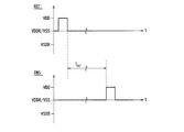
ここで、図7および図8を参照し、本実施形態にかかる光センサの動作について説明する。図7は、光センサへ配線RSTから供給されるリセット信号と配線RWSから供給される読み出し信号の波形をそれぞれ示すタイミングチャートである。図8は、第1の実施形態の光センサにおける入力信号(RST,RWS)とVINTとの関係を示す波形図である。 Here, the operation of the optical sensor according to the present embodiment will be described with reference to FIGS. FIG. 7 is a timing chart showing waveforms of a reset signal supplied from the wiring RST and a readout signal supplied from the wiring RWS to the optical sensor. FIG. 8 is a waveform diagram showing the relationship between the input signals (RST, RWS) and V INT in the photosensor of the first embodiment.
図7および図8に示す例では、リセット信号のハイレベルVRST.Hは0V、ローレベルVRST.Lは−4Vである。この例では、リセット信号のハイレベルVRST.HはVSSに等しい。また、読み出し信号のハイレベルVRWS.Hは4V、ローレベルVRWS.Lは−4Vである。この例では、読み出し信号のハイレベルVRWS.HがVDDに等しく、ローレベルVRWS.LがVSSRに等しい。 In the example shown in FIGS. 7 and 8, the high level V RST.H of the reset signal is 0V, and the low level V RST.L is −4V. In this example, the high level V RST.H of the reset signal is equal to V SS . The high level V RWS.H of the read signal is 4V, and the low level V RWS.L is −4V. In this example, the high level V RWS.H of the read signal is equal to V DD and the low level V RWS.L is equal to V SSR .
まず、センサロウドライバ5から配線RSTへ供給されるリセット信号がローレベル(−4V)から立ち上がってハイレベル(0V)になると、フォトダイオードD1は順方向バイアスとなる。このとき、トランジスタM2のゲート電極の電位VINTはトランジスタM2の閾値電圧より低いので、トランジスタM2は非導通状態となっている。また、pチャネル薄膜トランジスタM8のゲート電極の電位は読み出し信号のローレベル(−4V)と等しいので、pチャネル薄膜トランジスタM8は導通状態となっている。このため、フォトダイオードD2もリセット信号によってリセットされる。 First, when the reset signal supplied from the sensor row driver 5 to the wiring RST rises from the low level (−4V) and goes to the high level (0V), the photodiode D1 becomes a forward bias. At this time, since the potential V INT of the gate electrode of the transistor M2 is lower than the threshold voltage of the transistor M2, the transistor M2 is non-conductive. In addition, since the potential of the gate electrode of the p-channel thin film transistor M8 is equal to the low level (−4 V) of the read signal, the p-channel thin film transistor M8 is in a conductive state. For this reason, the photodiode D2 is also reset by the reset signal.
次に、リセット信号がローレベルVRST.Lに戻ることにより、光電流の積分期間(図8に示す期間TINT)が始まる。積分期間においては、フォトダイオードD1,D2は逆バイアスとなり、電流がコンデンサCINTから流れ出し、コンデンサCINTを放電させる。このとき、フォトダイオードD1により、入射光によって生じる光電流IPHOTOと暗電流IDARKとの和が蓄積ノードINTから流れ出す。一方、フォトダイオードD2により、暗電流−IDARKが、pチャネル薄膜トランジスタM8を介して、蓄積ノードINTから流れ出す。この結果、実質的に、コンデンサCINTから蓄積ノードINTへ流れ出す電流は、光電流IPHOTOの分だけとなる。積分期間においても、VINTがトランジスタM2の閾値電圧より低いので、トランジスタM2は非導通状態となっている。 Next, when the reset signal returns to the low level V RST.L , the photocurrent integration period (period T INT shown in FIG. 8) starts. In the integration period, the photodiode D1, D2 becomes reverse biased, current flows from the capacitor C INT, discharge capacitor C INT. At this time, the sum of the photocurrent I PHOTO and the dark current I DARK generated by the incident light flows out of the storage node INT by the photodiode D1. On the other hand, the dark current -I DARK flows out of the storage node INT via the p-channel thin film transistor M8 by the photodiode D2. As a result, the current that flows from the capacitor C INT to the storage node INT is substantially equal to the photocurrent I PHOTO . Even during the integration period, since V INT is lower than the threshold voltage of the transistor M2, the transistor M2 is non-conductive.
積分期間が終わると、図7に示すように、読み出し信号RWSが立ち上がることにより、読み出し期間が始まる。なお、読み出し期間は、読み出し信号RWSがハイレベルの間、継続する。読み出し期間においては、pチャネル薄膜トランジスタM8のゲートの電位は、読み出し信号VRWSと等しい。よって、pチャネル薄膜トランジスタM8のゲートの電位が閾値電圧よりも高くなることにより、pチャネル薄膜トランジスタM8は非導通状態となる。このため、読み出し信号RWSが供給されることによって、フォトダイオードD2が順バイアスになることはない。 When the integration period ends, as shown in FIG. 7, the readout signal RWS rises to start the readout period. Note that the read period continues while the read signal RWS is at a high level. In the read period, the gate potential of the p-channel thin film transistor M8 is equal to the read signal V RWS . Therefore, when the potential of the gate of the p-channel thin film transistor M8 becomes higher than the threshold voltage, the p-channel thin film transistor M8 is turned off. For this reason, the photodiode D2 is not forward-biased by supplying the read signal RWS.
また、コンデンサCINTに対して電荷注入が起こる。この結果、トランジスタM2のゲート電極の電位VINTが、トランジスタM2の閾値電圧よりも高くなる。これにより、トランジスタM2は導通状態となる。例えば、配線OUTの端部にバイアストランジスタM3(図示せず)を設けることにより、トランジスタM2およびM3はソースフォロアアンプとして機能する。すなわち、トランジスタM3のドレインからの出力配線SOUTからの出力信号電圧は、積分期間にフォトダイオードD1へ入射した光による光電流IPHOTOの積分値に相当する。 In addition, charge injection occurs to the capacitor C INT . As a result, the potential V INT of the gate electrode of the transistor M2 becomes higher than the threshold voltage of the transistor M2. As a result, the transistor M2 becomes conductive. For example, by providing a bias transistor M3 (not shown) at the end of the wiring OUT, the transistors M2 and M3 function as a source follower amplifier. That is, the output signal voltage from the output wiring SOUT from the drain of the transistor M3 corresponds to the integrated value of the photocurrent I PHOTO caused by the light incident on the photodiode D1 during the integration period.
なお、図8において、破線で示した波形は、フォトダイオードD1に光の入射が少ない場合の電位VINTの変化を表し、実線で示した波形は、フォトダイオードD1に外光が入射した場合の電位VINTの変化を表している。図8のΔVが、フォトダイオードD1からの光電流IPHOTOの積分値に比例した電位差である。 In FIG. 8, a waveform indicated by a broken line represents a change in the potential V INT when light incident on the photodiode D1 is small, and a waveform indicated by a solid line represents the case where external light is incident on the photodiode D1. This represents a change in the potential V INT . ΔV in FIG. 8 is a potential difference proportional to the integral value of the photocurrent I PHOTO from the photodiode D1.
本実施形態にかかる光センサは、上述のとおり、フォトダイオードD1の光電流IPHOTO分のみをコンデンサCINTへ充放電するので、暗電流IDARKの大きさに関わりなく、外光の強度を正確に検出することができる。また、暗電流IDARKがコンデンサCINTから放電されないので、ダイナミックレンジを広くとることが可能となる。これにより、環境温度に影響されることなく外光の強度を高精度に検出できる光センサを実現することが可能となる。 As described above, the photosensor according to the present embodiment charges and discharges only the photocurrent I PHOTO of the photodiode D1 to and from the capacitor CINT , so that the intensity of external light is accurately determined regardless of the magnitude of the dark current I DARK. Can be detected. Further, since the dark current I DARK is not discharged from the capacitor C INT , a wide dynamic range can be obtained. As a result, it is possible to realize an optical sensor that can detect the intensity of external light with high accuracy without being affected by the environmental temperature.
また、参照電圧配線VCの電圧VCは、リセット信号のハイレベルVRST.Hよりも高ければよいことから、参照電圧配線VCにはDC電源を使用することができる。 Further, since the voltage V C of the reference voltage wiring VC only needs to be higher than the high level V RST.H of the reset signal, a DC power supply can be used for the reference voltage wiring VC.
さらに、配線RWSにより読み出し信号が供給されると、pチャネル薄膜トランジスタM8が非導通状態となることによりフォトダイオードD2が無効化されるため、読み出し期間においてフォトダイオードD2を逆バイアスに保持しておく必要がない。このため、フォトダイオードD2のカソードの接続先である参照電圧配線VCの電圧を高く設定する必要がない。 Further, when a read signal is supplied through the wiring RWS, the p-channel thin film transistor M8 is turned off, so that the photodiode D2 is invalidated. Therefore, it is necessary to hold the photodiode D2 in a reverse bias during the read period. There is no. For this reason, it is not necessary to set the voltage of the reference voltage wiring VC, which is the connection destination of the cathode of the photodiode D2, high.
このように、読み出し信号の電圧設計の自由度が高まるため、例えば、読み出し信号を供給する配線RWSに増幅素子を接続した構成も可能になる。図3は、図1に示す光センサにおいて、コンデンサCINTの代わりに増幅素子を用いた場合の回路構成の例を示す図である。 Thus, since the degree of freedom in designing the voltage of the read signal is increased, for example, a configuration in which an amplifying element is connected to the wiring RWS that supplies the read signal becomes possible. FIG. 3 is a diagram illustrating an example of a circuit configuration when an amplifying element is used instead of the capacitor CINT in the optical sensor illustrated in FIG.
図3に示す光センサは、増幅素子の一例であるpチャネル薄膜トランジスタM10を備える。pチャネル薄膜トランジスタM10のドレインは蓄積ノードINTに、ソースはトランジスタM2のゲートに、ゲートは読み出し信号を供給する配線RWSに接続されている。 The optical sensor shown in FIG. 3 includes a p-channel thin film transistor M10 that is an example of an amplifying element. The drain of the p-channel thin film transistor M10 is connected to the storage node INT, the source is connected to the gate of the transistor M2, and the gate is connected to the wiring RWS for supplying a read signal.
図4に示す光センサは、図2に示す光センサにおいて、コンデンサCINTの代わりにpチャネル薄膜トランジスタM10を用いた場合の回路構成の例を示す図である。pチャネル薄膜トランジスタM11のドレインは蓄積ノードINTに、ソースはトランジスタM2のゲートに、ゲートは読み出し信号を供給する配線RWSに接続されている。 The optical sensor shown in FIG. 4 is a diagram showing an example of a circuit configuration when a p-channel thin film transistor M10 is used instead of the capacitor CINT in the optical sensor shown in FIG. The drain of the p-channel thin film transistor M11 is connected to the storage node INT, the source is connected to the gate of the transistor M2, and the gate is connected to the wiring RWS for supplying a read signal.
図3、4に例示する増幅素子(pチャネル薄膜トランジスタM10、M11)は、蓄積ノードINTの電位を増幅する増幅素子の一例である。増幅素子としては、pチャネル薄膜トランジスタの他に、例えば、可変コンデンサ(詳細は後述)、nチャネル薄膜トランジスタまたはチャネル上にゲート電極を備えたダイオード等を用いることができる。 The amplifying elements (p-channel thin film transistors M10 and M11) illustrated in FIGS. 3 and 4 are examples of amplifying elements that amplify the potential of the storage node INT. In addition to the p-channel thin film transistor, for example, a variable capacitor (details will be described later), an n-channel thin film transistor, a diode having a gate electrode on the channel, or the like can be used as the amplifying element.
pチャネル薄膜トランジスタM10、M11により、蓄積ノードINTの電位を増幅して、読み出すことができる。これらのpチャネル薄膜トランジスタM10、M11のような増幅素子の動作条件は、読み出し信号のローレベルVRWS.Lが、蓄積ノードの電位VINTとpチャネル薄膜トランジスタM10またはM11の閾値Vthとを加算した値を超えないことである。センシング期間(リセット信号が供給されてから読み出し信号が供給されるまでの期間)ではpチャネル薄膜トランジスタM10、M11は導通状態であり、読み出し期間に導通状態から非道通状態に変化する(動作の詳細は後述する)。読み出し信号は、参照用電圧VCに関わらず自由に設定できるので、図3、4に例示するように、増幅素子を用いた構成が可能になる。 The potential of the storage node INT can be amplified and read by the p-channel thin film transistors M10 and M11. The operating conditions of the amplifying elements such as the p-channel thin film transistors M10 and M11 are values obtained by adding the low level V RWS.L of the read signal to the potential V INT of the storage node and the threshold Vth of the p-channel thin film transistor M10 or M11. Is not to exceed. In the sensing period (period from when the reset signal is supplied to when the read signal is supplied), the p-channel thin film transistors M10 and M11 are in the conductive state, and change from the conductive state to the non-conductive state during the read period (details of operation are Will be described later). Since the read signal can be freely set regardless of the reference voltage VC, a configuration using an amplifying element is possible as illustrated in FIGS.
[第2の実施形態]
最初に、図5および図6を参照しながら、本発明の第1の実施形態にかかる光センサを備える液晶表示装置の構成について説明する。
[Second Embodiment]
First, the configuration of a liquid crystal display device including an optical sensor according to the first embodiment of the present invention will be described with reference to FIGS. 5 and 6.
図5は、本発明の一実施形態にかかる液晶表示装置が備えるアクティブマトリクス基板100の概略構成を示すブロック図である。図5に示すように、アクティブマトリクス基板100は、ガラス基板上に、画素領域1、ディスプレイゲートドライバ2、ディスプレイソースドライバ3、センサカラム(column)ドライバ4、センサロウ(row)ドライバ5、バッファアンプ6、FPCコネクタ7を少なくとも備えている。また、画素領域1内の光検出素子(後述)で取り込まれた画像信号を処理するための信号処理回路8が、前記FPCコネクタ7とFPC9とを介して、アクティブマトリクス基板100に接続されている。
FIG. 5 is a block diagram showing a schematic configuration of the
なお、アクティブマトリクス基板100上の上記の構成部材は、半導体プロセスによってガラス基板上にモノリシックに形成することも可能である。あるいは、上記の構成部材のうちのアンプやドライバ類を、例えばCOG(Chip On Glass)技術等によってガラス基板上に実装した構成としても良い。あるいは、図5においてアクティブマトリクス基板100上に示した上記の構成部材の少なくとも一部が、FPC9上に実装されることも考えられる。アクティブマトリクス基板100は、全面に対向電極が形成された対向基板(図示せず)と貼り合わされ、その間隙に液晶材料が封入される。
Note that the above-described components on the
画素領域1は、画像を表示するために、複数の画素が形成された領域である。本実施形態では、画素領域1における各画素内には、画像を取り込むための光センサが設けられている。図6は、アクティブマトリクス基板100の画素領域1における画素と光センサとの配置を示す等価回路図である。図6の例では、1つの画素が、R(赤)、G(緑)、B(青)の3色の絵素によって形成され、この3絵素で構成される1つの画素内に、2つのフォトダイオードD1,D2とコンデンサCINTと薄膜トランジスタM2とpチャネル薄膜トランジスタM8によって構成される1つの光センサが設けられている。画素領域1は、M行×N列のマトリクス状に配置された画素と、同じくM行×N列のマトリクス状に配置された光センサとを有する。なお、上述のとおり、絵素数は、M×3Nである。
The
このため、図6に示すように、画素領域1は、画素用の配線として、マトリクス状に配置されたゲート線GLおよびソース線COLを有している。ゲート線GLは、ディスプレイゲートドライバ2に接続されている。ソース線COLは、ディスプレイソースドライバ3に接続されている。なお、ゲート線GLは、画素領域1内にM行設けられている。以下、個々のゲート線GLを区別して説明する必要がある場合は、GLi(i=1〜M)のように表記する。一方、ソース線COLは、上述のとおり、1つの画素内の3絵素にそれぞれ画像データを供給するために、1画素につき3本ずつ設けられている。ソース線COLを個々に区別して説明する必要がある場合は、COLrj,COLgj,COLbj(j=1〜N)のように表記する。
For this reason, as shown in FIG. 6, the
ゲート線GLとソース線COLとの交点には、画素用のスイッチング素子として、薄膜トランジスタ(TFT)M1が設けられている。なお、図6では、赤色、緑色、青色のそれぞれの絵素に設けられている薄膜トランジスタM1を、M1r,M1g,M1bと表記している。薄膜トランジスタM1のゲート電極はゲート線GLへ、ソース電極はソース線COLへ、ドレイン電極は図示しない画素電極へ、それぞれ接続されている。これにより、図6に示すように、薄膜トランジスタM1のドレイン電極と対向電極(VCOM)との間に液晶容量LCが形成される。また、ドレイン電極とTFTCOMとの間に補助容量LSが形成されている。 A thin film transistor (TFT) M1 is provided as a pixel switching element at the intersection of the gate line GL and the source line COL. In FIG. 6, the thin film transistor M1 provided in each of the red, green, and blue picture elements is denoted as M1r, M1g, and M1b. The thin film transistor M1 has a gate electrode connected to the gate line GL, a source electrode connected to the source line COL, and a drain electrode connected to a pixel electrode (not shown). As a result, as shown in FIG. 6, a liquid crystal capacitor LC is formed between the drain electrode of the thin film transistor M1 and the counter electrode (VCOM). Further, an auxiliary capacitor LS is formed between the drain electrode and the TFTCOM.
図6において、1本のゲート線GLiと1本のソース線COLrjとの交点に接続された薄膜トランジスタM1rによって駆動される絵素は、この絵素に対応するように赤色のカラーフィルタが設けられ、ソース線COLrjを介してディスプレイソースドライバ3から赤色の画像データが供給されることにより、赤色の絵素として機能する。また、ゲート線GLiとソース線COLgjとの交点に接続された薄膜トランジスタM1gによって駆動される絵素は、この絵素に対応するように緑色のカラーフィルタが設けられ、ソース線COLgjを介してディスプレイソースドライバ3から緑色の画像データが供給されることにより、緑色の絵素として機能する。さらに、ゲート線GLiとソース線COLbjとの交点に接続された薄膜トランジスタM1bによって駆動される絵素は、この絵素に対応するように青色のカラーフィルタが設けられ、ソース線COLbjを介してディスプレイソースドライバ3から青色の画像データが供給されることにより、青色の絵素として機能する。 In FIG. 6, a picture element driven by the thin film transistor M1r connected to the intersection of one gate line GLi and one source line COLrj is provided with a red color filter so as to correspond to this picture element. When red image data is supplied from the display source driver 3 via the source line COLrj, it functions as a red picture element. Further, a picture element driven by the thin film transistor M1g connected to the intersection of the gate line GLi and the source line COLgj is provided with a green color filter so as to correspond to the picture element, and a display source is provided via the source line COLgj. When green image data is supplied from the driver 3, it functions as a green picture element. Further, the pixel driven by the thin film transistor M1b connected to the intersection of the gate line GLi and the source line COLbj is provided with a blue color filter so as to correspond to this pixel, and the display source is connected via the source line COLbj. When blue image data is supplied from the driver 3, it functions as a blue picture element.
なお、図6の例では、光センサは、画素領域1において、1画素(3絵素)に1つの割合で設けられている。ただし、画素と光センサの配置割合は、この例のみに限定されず、任意である。例えば、1絵素につき1つの光センサが配置されていても良いし、複数画素に対して1つの光センサが配置された構成であっても良い。
In the example of FIG. 6, one photosensor is provided for each pixel (three picture elements) in the
光センサは、図6に示すように、フォトダイオードD1,D2と、コンデンサCINTと、薄膜トランジスタM2とpチャネル薄膜トランジスタM8を備えている。図6に示す光センサは、図1に示した回路構成と同様である。 図6の例では、ソース線COLrが、センサカラムドライバ4から定電圧VDDを光センサへ供給するための配線VDDを兼ねている。また、ソース線COLgが、センサ出力用の配線OUTを兼ねている。 As shown in FIG. 6, the optical sensor includes photodiodes D1 and D2, a capacitor CINT , a thin film transistor M2, and a p-channel thin film transistor M8. The optical sensor shown in FIG. 6 has the same circuit configuration as that shown in FIG. In the example of FIG. 6, the source line COLr also serves as the wiring VDD for supplying the constant voltage V DD from the sensor column driver 4 to the photosensor. Further, the source line COLg also serves as the sensor output wiring OUT.
フォトダイオードD1のアノードには、リセット信号を供給するための配線RSTが接続されている。フォトダイオードD1とpチャネル薄膜トランジスタM8とは直列に接続されており、フォトダイオードD1のカソードとpチャネル薄膜トランジスタM8のドレインとの間に、トランジスタM2のゲートと、コンデンサCINTの電極の一方が接続されている。pチャネル薄膜トランジスタM8のソースは、フォトダイオードD2のアノードに接続されている。pチャネル薄膜トランジスタM8のゲートは、配線RWSに接続されている。フォトダイオードD2のカソードは、参照電圧配線VCに接続されている。 A wiring RST for supplying a reset signal is connected to the anode of the photodiode D1. The photodiode D1 and the p-channel thin film transistor M8 are connected in series, and one of the gate of the transistor M2 and the electrode of the capacitor CINT is connected between the cathode of the photodiode D1 and the drain of the p-channel thin film transistor M8. ing. The source of the p-channel thin film transistor M8 is connected to the anode of the photodiode D2. The gate of the p-channel thin film transistor M8 is connected to the wiring RWS. The cathode of the photodiode D2 is connected to the reference voltage wiring VC.
トランジスタM2のドレインは配線VDDに接続され、ソースは配線OUTに接続されている。配線RST,RWSは、センサロウドライバ5に接続されている。これらの配線RST,RWSは1行毎に設けられているので、以降、各配線を区別する必要がある場合は、RSTi,RWSi(i=1〜M)のように表記する。 The drain of the transistor M2 is connected to the wiring VDD, and the source is connected to the wiring OUT. The wirings RST and RWS are connected to the sensor row driver 5. Since these wirings RST and RWS are provided for each row, hereinafter, when it is necessary to distinguish each wiring, they are represented as RSTi and RWSi (i = 1 to M).
センサロウドライバ5は、所定の時間間隔(trow)で、図6に示した配線RSTiとRWSiとの組を順次選択していく。これにより、画素領域1において信号電荷を読み出すべき光センサの行(row)が順次選択される。
The sensor row driver 5 sequentially selects the pair of wirings RSTi and RWSi shown in FIG. 6 at a predetermined time interval (t row ). As a result, the rows of photosensors from which signal charges are to be read out in the
なお、図6に示すように、配線OUTの端部には、絶縁ゲート型電界効果トランジスタM3のドレインが接続されている。また、このトランジスタM3のドレインには、出力配線SOUTが接続され、トランジスタM3のドレインの電位VSOUTが、光センサからの出力信号としてセンサカラムドライバ4へ出力される。トランジスタM3のソースは、配線VSSに接続されている。トランジスタM3のゲートは、参照電圧配線VBを介して、参照電圧電源(図示せず)に接続されている。 As shown in FIG. 6, the drain of the insulated gate field effect transistor M3 is connected to the end of the wiring OUT. Further, the output wiring SOUT is connected to the drain of the transistor M3, and the potential V SOUT of the drain of the transistor M3 is output to the sensor column driver 4 as an output signal from the photosensor. The source of the transistor M3 is connected to the wiring VSS. The gate of the transistor M3 is connected to a reference voltage power supply (not shown) via the reference voltage wiring VB.
本実施形態にかかる光センサの動作は、図7および図8に示した動作と同様である。 The operation of the optical sensor according to the present embodiment is the same as the operation shown in FIGS.
図7および図8に示した動作のように、リセットパルスによる初期化と、積分期間における光電流の積分と、読み出し期間におけるセンサ出力の読み出しとを周期的に行うことにより、各画素の光センサ出力を得ることができる。 As in the operation shown in FIGS. 7 and 8, the initialization by the reset pulse, the integration of the photocurrent in the integration period, and the reading of the sensor output in the readout period are performed periodically, so that the optical sensor of each pixel Output can be obtained.
本実施形態にかかる表示装置の各画素に設けられた光センサは、上述のとおり、フォトダイオードD1の光電流IPHOTO分のみをコンデンサCINTへ充放電するので、暗電流IDARKの大きさに関わりなく、外光の強度を正確に検出することができる。また、暗電流IDARKがコンデンサCINTから放電されないので、ダイナミックレンジを広くとることが可能となる。これにより、環境温度に影響されることなく外光の強度を高精度に検出できる光センサを実現することが可能となる。 Since the photosensor provided in each pixel of the display device according to the present embodiment charges and discharges only the photocurrent I PHOTO of the photodiode D1 to the capacitor CINT as described above, the magnitude of the dark current I DARK is increased. Regardless, the intensity of outside light can be accurately detected. Further, since the dark current I DARK is not discharged from the capacitor C INT , a wide dynamic range can be obtained. As a result, it is possible to realize an optical sensor that can detect the intensity of external light with high accuracy without being affected by the environmental temperature.
また、参照電圧配線VCの電圧は、リセット信号のハイレベルVRST.Hよりも高ければよいことから、参照電圧配線VCにはDC電源を使用することができる。 Further, since the voltage of the reference voltage wiring VC only needs to be higher than the high level V RST.H of the reset signal, a DC power source can be used for the reference voltage wiring VC.
さらに、読み出し信号RWSが供給されると、pチャネル薄膜トランジスタM8が非導通状態となることによりフォトダイオードD2が無効化されるため、読み出し期間においてフォトダイオードD2を逆バイアスに保持しておく必要がない。このため、フォトダイオードD2のカソードの接続先である参照電圧配線VCの電圧を高く設定する必要がない。 Further, when the read signal RWS is supplied, the photodiode D2 is invalidated because the p-channel thin film transistor M8 is turned off, so that it is not necessary to hold the photodiode D2 in reverse bias during the read period. . For this reason, it is not necessary to set the voltage of the reference voltage wiring VC, which is the connection destination of the cathode of the photodiode D2, high.
また、参照電圧配線VCに代えて、既存の配線を用いて回路を構成することもできる。例えば、特性安定化のためにフォトダイオード上に形成された透明電極ITOで形成されたシールド電極を用いて回路を構成することもできる。図20は、本実施形態にかかる光センサの平面構造の一例を示す平面図である。 In addition, a circuit can be configured by using existing wiring instead of the reference voltage wiring VC. For example, a circuit can be configured using a shield electrode formed of a transparent electrode ITO formed on a photodiode for stabilization of characteristics. FIG. 20 is a plan view illustrating an example of a planar structure of the photosensor according to the present embodiment.
図20に示すように、本実施形態にかかる光センサは、ソース線COLgとCOLbとの間の領域にトランジスタM2を備えている。フォトダイオードD1は、ベースとなるシリコン膜に、p型半導体領域102pと、i型半導体領域102iと、n型半導体領域102nとが直列に形成された、ラテラル構造のPINダイオードである。p型半導体領域102pは、フォトダイオードD1のアノードとなり、配線108およびコンタクト109,110を介して配線RSTに接続される。n型半導体領域102nは、フォトダイオードD1のカソードとなり、シリコン膜の延設部107,コンタクト105,106、および配線104を介して、トランジスタM2のゲート電極101に接続される。
As shown in FIG. 20, the photosensor according to the present embodiment includes a transistor M2 in a region between the source lines COLg and COLb. The photodiode D1 is a lateral structure PIN diode in which a p-
フォトダイオードD2は、フォトダイオードD1と同様に、ベースとなるシリコン膜に、p型半導体領域102pと、i型半導体領域102iと、n型半導体領域102nとが直列に形成された、ラテラル構造のPINダイオードである。ただし、n型半導体領域102n(カソード)が、配線115およびコンタクト116,117を介してシールド電極114に接続される。また、p型半導体領域102p(アノード)が、シリコン膜の延設部107,コンタクト105,106、および配線104を介して、トランジスタM2のゲート電極101に接続される。
Similar to the photodiode D1, the photodiode D2 has a lateral structure PIN in which a p-
この構成において、配線RST,RWSは、トランジスタM2のゲート電極101と同じ金属により同じ工程で形成されている。また、配線104,108は、ソース線COLと同じ金属により同じ工程で形成されている。フォトダイオードD1,2の背面には、バックライト光がセンサへ入射することを防止するための遮光膜113が設けられている。
In this configuration, the wirings RST and RWS are formed of the same metal as the
なお、本実施形態においては、pチャネル薄膜トランジスタM8を備えた光センサを開示したが、図17に示すように、pチャネル薄膜トランジスタM8に代えてnチャネル薄膜トランジスタM9を備える構成としても良い。図17においては、nチャネル薄膜トランジスタM9のゲートは、配線RWSではなく、フォトダイオードD2のカソードと同様に、参照電圧配線VCに接続されている。なお、参照電圧配線VCの電圧は、リセット信号のハイレベルVRST.Hよりも高く、読み出し信号のハイレベルVRWS.Hよりも低ければ良い。 In the present embodiment, the optical sensor including the p-channel thin film transistor M8 is disclosed. However, as illustrated in FIG. 17, an n-channel thin film transistor M9 may be provided instead of the p-channel thin film transistor M8. In FIG. 17, the gate of the n-channel thin film transistor M9 is connected not to the wiring RWS but to the reference voltage wiring VC similarly to the cathode of the photodiode D2. Note that the voltage of the reference voltage wiring VC may be higher than the high level V RST.H of the reset signal and lower than the high level V RWS.H of the read signal.
読み出し信号RWSが立ち上がると、VINTの電位が突き上げられる。この直後においては、突き上げられたVINTの電位が、VCからnチャネル薄膜トランジスタM9の閾値Vthを減算した値よりも高くなった時点で、nチャネル薄膜トランジスタM9にオフ電圧がかかる。つまり、オフ電圧がかかった時点で、nチャネル薄膜トランジスタM9は非導通状態となる。これにより、読み出し信号RWSによって、VINTをVCよりも高い電位に突き上げることができる。 When the read signal RWS rises, the potential of V INT is pushed up. Immediately after this, the off-voltage is applied to the n-channel thin film transistor M9 when the pushed potential of V INT becomes higher than the value obtained by subtracting the threshold value Vth of the n-channel thin film transistor M9 from VC. That is, when the off voltage is applied, the n-channel thin film transistor M9 is turned off. Thereby, V INT can be pushed up to a potential higher than VC by the read signal RWS.
この構成によっても、フォトダイオードD1の光電流IPHOTO分のみをコンデンサCINTへ充放電するので、暗電流IDARKの大きさに関わりなく、外光の強度を正確に検出することができる。また、暗電流IDARKがコンデンサCINTから放電されないので、ダイナミックレンジを広くとることが可能となる。これにより、環境温度に影響されることなく外光の強度を高精度に検出できる光センサを実現することが可能となる。 Also with this configuration, only the photocurrent I PHOTO of the photodiode D1 is charged to and discharged from the capacitor CINT , so that the intensity of external light can be accurately detected regardless of the magnitude of the dark current I DARK . Further, since the dark current I DARK is not discharged from the capacitor C INT , a wide dynamic range can be obtained. As a result, it is possible to realize an optical sensor that can detect the intensity of external light with high accuracy without being affected by the environmental temperature.
なお、図17に示した構成は、図6に示した構成に対して、以下の利点を有する。図17の構成の場合は、読み出し信号RWSの電圧(VRWS.HまたはVRWS.L)を設定する場合の自由度が高い。これに対して、図6に示した構成は、読み出し信号RWSのローレベルVRWS.Lを、リセット信号のハイレベルVRST.Hよりも小さく設定する必要がある。 The configuration shown in FIG. 17 has the following advantages over the configuration shown in FIG. In the case of the configuration of FIG. 17, the degree of freedom in setting the voltage (V RWS.H or V RWS.L ) of the read signal RWS is high. On the other hand, in the configuration shown in FIG. 6, it is necessary to set the low level V RWS.L of the read signal RWS smaller than the high level V RST.H of the reset signal.
図21は、図17にかかる光センサの平面構造の一例を示す平面図である。なお、以下の図21の説明においては、上述の図20で説明した構成と同様の機能を有する構成については、同じ参照符号を付記し、その詳細な説明を省略する。図21に示すように、nチャネル薄膜トランジスタM9のゲート電極は、コンタクト119,120および配線118を介して、シールド電極114に接続される。
FIG. 21 is a plan view showing an example of a planar structure of the photosensor according to FIG. In the following description of FIG. 21, the same reference numerals are given to configurations having the same functions as those described in FIG. 20, and detailed descriptions thereof are omitted. As shown in FIG. 21, the gate electrode of the n-channel thin film transistor M9 is connected to the
なお、本実施形態では、前述したように、ソース線COLr,COLg,COLbを光センサ用の配線VDD,OUT,VSSとして共用しているので、図9に示すように、ソース線COLr,COLg,COLbを介して表示用の画像データ信号を入力するタイミングと、センサ出力を読み出すタイミングとを区別する必要がある。図9の例では、水平走査期間において表示用画像データ信号の入力が終わった後に、水平ブランキング期間等を利用してセンサ出力の読み出しが行われる。すなわち、表示用画像データ信号の入力が終わった後に、ソース線COLrには定電圧VDDが印加される。 In the present embodiment, as described above, the source lines COLr, COLg, and COLb are shared as the photosensor wirings VDD, OUT, and VSS. Therefore, as shown in FIG. 9, the source lines COLr, COLg, It is necessary to distinguish between the timing of inputting the image data signal for display via COLb and the timing of reading the sensor output. In the example of FIG. 9, the sensor output is read using the horizontal blanking period after the display image data signal has been input in the horizontal scanning period. That is, after the display image data signal has been input, the constant voltage V DD is applied to the source line COLr.
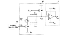
センサカラムドライバ4は、図5に示すように、センサ画素読み出し回路41と、センサカラムアンプ42と、センサカラム走査回路43とを含む。センサ画素読み出し回路41には、画素領域1からセンサ出力VSOUTを出力する配線SOUT(図10参照)が接続されている。図5において、配線SOUTj(j=1〜N)により出力されるセンサ出力を、VSOUTjと表記している。センサ画素読み出し回路41は、センサ出力VSOUTjのピークホールド電圧VSjを、センサカラムアンプ42へ出力する。センサカラムアンプ42は、画素領域1のN列の光センサにそれぞれ対応するN個のカラムアンプを内蔵しており、個々のカラムアンプでピークホールド電圧VSj(j=1〜N)を増幅し、VCOUTとしてバッファアンプ6へ出力する。センサカラム走査回路43は、センサカラムアンプ42のカラムアンプをバッファアンプ6への出力へ順次接続するために、カラムセレクト信号CSj(j=1〜N)を、センサカラムアンプ42へ出力する。
As shown in FIG. 5, the sensor column driver 4 includes a sensor pixel readout circuit 41, a
ここで、図10および図11を参照し、画素領域1からセンサ出力VSOUTが読み出された後のセンサカラムドライバ4およびバッファアンプ6の動作について説明する。図10は、センサ画素読み出し回路41の内部構成を示す回路図である。図11は、読み出し信号VRWSと、センサ出力VSOUTと、センサ画素読み出し回路の出力VSとの関係を示す波形図である。前述のように、読み出し信号がハイレベルVRWS.Hになったとき、トランジスタM2が導通することにより、トランジスタM2,M3によりソースフォロアアンプが形成され、センサ出力VSOUTがセンサ画素読み出し回路41のサンプルキャパシタCSAMに蓄積される。これにより、読み出し信号がローレベルVRWS.Lになった後も、その行の選択期間(trow)中、センサ画素読み出し回路41からセンサカラムアンプ42への出力電圧VSは、図11に示すように、センサ出力VSOUTのピーク値と等しいレベルに保持される。
Here, the operations of the sensor column driver 4 and the
次に、センサカラムアンプ42の動作について、図12を参照しながら説明する。図12に示すように、センサ画素読み出し回路41から、各列の出力電圧VSj(j=1〜N)が、センサカラムアンプ42のN個のカラムアンプへ入力される。図12に示すように、各カラムアンプは、トランジスタM6,M7から構成されている。センサカラム走査回路43によって生成されるカラムセレクト信号CSjが、1つの行の選択期間(trow)中に、N列のカラムのそれぞれに対して順次ONとなることにより、センサカラムアンプ42中のN個のカラムアンプのうちいずれか1つのみのトランジスタM6がONとなり、そのトランジスタM6を介して、各列の出力電圧VSj(j=1〜N)のいずれかのみが、センサカラムアンプ42からの出力VCOUTとして出力される。バッファアンプ6は、センサカラムアンプ42から出力されたVCOUTをさらに増幅し、パネル出力(光センサ信号)Voutとして信号処理回路8へ出力する。
Next, the operation of the
なお、センサカラム走査回路43は、上述のように光センサの列を1列ずつ走査するようにしても良いが、これに限定されず、光センサの列をインタレース走査する構成としても良い。また、センサカラム走査回路43が、例えば4相等の多相駆動走査回路として形成されていても良い。 The sensor column scanning circuit 43 may scan the optical sensor columns one by one as described above, but is not limited to this, and may be configured to interlace scan the optical sensor columns. Further, the sensor column scanning circuit 43 may be formed as a multi-phase driving scanning circuit such as a four-phase.
以上の構成により、本実施形態にかかる表示装置は、画素領域1において画素毎に形成されたフォトダイオードD1の受光量に応じたパネル出力VOUTを得る。パネル出力VOUTは、信号処理回路8に送られてA/D変換され、パネル出力データとしてメモリ(図示せず)に蓄積される。つまり、このメモリには、画素領域1の画素数(光センサ数)と同数のパネル出力データが蓄積されることとなる。信号処理回路8では、メモリに蓄積されたパネル出力データを用いて、画像取り込みやタッチ領域の検出等の各種信号処理を行う。なお、本実施形態では、信号処理回路8のメモリに、画素領域1の画素数(光センサ数)と同数のパネル出力データを蓄積するものとしたが、メモリ容量等の制約により、必ずしも画素数と同数のパネル出力データを蓄積することを要しない。
With the above configuration, the display device according to the present embodiment obtains a panel output V OUT corresponding to the amount of light received by the photodiode D1 formed for each pixel in the
[第3の実施形態]
本発明の第3の実施形態にかかる表示装置について、以下に説明する。なお、前述の第2の実施形態において説明した構成と同様の機能を有する構成については、同じ参照符号を付記し、その詳細な説明を省略する。
[Third Embodiment]
A display device according to the third embodiment of the present invention will be described below. In addition, about the structure which has the same function as the structure demonstrated in the above-mentioned 2nd Embodiment, the same referential mark is attached and the detailed description is abbreviate | omitted.
図13は、第3の実施形態にかかる表示装置における一画素の構成を示す等価回路図である。図13に示すように、第3の実施形態にかかる表示装置の光センサは、フォトダイオードD1,D2、コンデンサCINT、薄膜トランジスタM2およびpチャネル薄膜トランジスタM8に加えて、薄膜トランジスタM4をさらに備えている。 FIG. 13 is an equivalent circuit diagram showing a configuration of one pixel in the display device according to the third embodiment. As shown in FIG. 13, the optical sensor of the display device according to the third embodiment further includes a thin film transistor M4 in addition to the photodiodes D1 and D2, the capacitor C INT , the thin film transistor M2, and the p-channel thin film transistor M8.
本実施形態の光センサにおいては、コンデンサCINTの一方の電極が、フォトダイオードD1のカソードとpチャネル薄膜トランジスタM8のドレインとの間と、薄膜トランジスタM2のゲート電極とに接続され、コンデンサCINTの他方の電極は、配線VDDに接続されている。また、薄膜トランジスタM2のドレインは配線VDDに接続され、ソースは薄膜トランジスタM4のドレインに接続されている。薄膜トランジスタM4のゲートは、読み出し信号配線RWSに接続されている。薄膜トランジスタM4のソースは、配線OUTに接続されている。なお、この例では、コンデンサCINTの電極の一つと、薄膜トランジスタM4のドレインとが、共に、共通の定電圧配線(配線VDD)に接続されている構成を示したが、これらが互いに異なる定電圧配線に接続された構成であっても構わない。 In the optical sensor of the present embodiment, one electrode of the capacitor C INT is the between the drain of the cathode and the p-channel thin film transistor M8 of the photodiode D1, is connected to the gate electrode of the thin film transistor M2, the other capacitor C INT Are connected to the wiring VDD. The drain of the thin film transistor M2 is connected to the wiring VDD, and the source is connected to the drain of the thin film transistor M4. The gate of the thin film transistor M4 is connected to the read signal wiring RWS. The source of the thin film transistor M4 is connected to the wiring OUT. In this example, one of the electrodes of the capacitor C INT and the drain of the thin film transistor M4 are both connected to a common constant voltage wiring (wiring VDD). However, these constant voltages are different from each other. It may be a configuration connected to wiring.
ここで、本実施形態にかかる光センサの動作について、図14および図15を参照しながら説明する。 Here, the operation of the photosensor according to the present embodiment will be described with reference to FIGS. 14 and 15.
図14は、光センサへ配線RSTから供給されるリセット信号と配線RWSから供給される読み出し信号の波形をそれぞれ示すタイミングチャートである。図15は、第3の実施形態の光センサにおける入力信号(RST,RWS)とVINTとの関係を示す波形図である。 FIG. 14 is a timing chart showing waveforms of a reset signal supplied from the wiring RST and a readout signal supplied from the wiring RWS to the optical sensor. FIG. 15 is a waveform diagram showing the relationship between input signals (RST, RWS) and V INT in the photosensor according to the third embodiment.
リセット信号のハイレベルVRST.Hは、薄膜トランジスタM2がオン状態になる電位に設定される。図14に示す例では、リセット信号のハイレベルVRST.Hは8Vである。また、リセット信号のローレベルVRST.Lは0Vである。この例では、リセット信号のハイレベルVRST.HはVDDに等しく、ローレベルVRST.LはVSSに等しい。また、読み出し信号のハイレベルVRWS.Hは8V、ローレベルVRWS.Lは0Vである。この例では、読み出し信号のハイレベルVRWS.HがVDDに等しく、ローレベルVRWS.LがVSSに等しい。 The high level V RST.H of the reset signal is set to a potential at which the thin film transistor M2 is turned on. In the example shown in FIG. 14, the high level V RST.H of the reset signal is 8V. The low level V RST.L of the reset signal is 0V. In this example, the high level V RST.H of the reset signal is equal to V DD and the low level V RST.L is equal to V SS . The high level V RWS.H of the read signal is 8V, and the low level V RWS.L is 0V. In this example, the high level V RWS.H of the read signal is equal to V DD and the low level V RWS.L is equal to V SS .
まず、センサロウドライバ5から配線RSTへ供給されるリセット信号がローレベル(0V)から立ち上がってハイレベル(8V)になると、フォトダイオードD1は順方向バイアスとなる。このとき、トランジスタM2はオン状態となるが、読み出し信号RWSがローレベルであり、トランジスタM4がオフ状態なので、配線OUTへの出力はない。 First, when the reset signal supplied from the sensor row driver 5 to the wiring RST rises from the low level (0 V) and goes to the high level (8 V), the photodiode D1 becomes a forward bias. At this time, the transistor M2 is turned on, but since the read signal RWS is at a low level and the transistor M4 is turned off, there is no output to the wiring OUT.
次に、リセット信号がローレベルVRST.Lに戻ることにより、光電流の積分期間(図15に示す期間TINT)が始まる。積分期間においては、フォトダイオードD1,D2は逆バイアスとなり、電流がコンデンサCINTから流れ出し、コンデンサCINTを放電させる。このとき、フォトダイオードD1により、入射光によって生じる光電流IPHOTOと暗電流IDARKとの和が蓄積ノードINTから流れ出す。一方、フォトダイオードD2により、暗電流−IDARKが蓄積ノードINTから流れ出す。この結果、実質的に、コンデンサCINTから蓄積ノードINTへ流れ出す電流は、光電流IPHOTOの分だけとなる。積分期間においても、VINTは、リセット電位(この例ではVRST.H=8V)から入射光の強さに応じて降下していく。しかし、トランジスタM4がオフ状態のため、配線OUTへのセンサ出力はない。なお、検出したい照度の上限値の光がフォトダイオードD1に照射された場合にセンサ出力が最も小さくなるように、すなわち、この場合にトランジスタM2のゲート電極の電位(VINT)が閾値をわずかに超える値となるように、センサ回路を設計することが望ましい。このように設計すれば、検出したい照度の上限値を超える光がフォトダイオードD1へ照射された場合には、VINTの値がトランジスタM2の閾値よりも低くなってトランジスタM2がオフ状態となるので、配線OUTへのセンサ出力はない。 Next, when the reset signal returns to the low level V RST.L , the photocurrent integration period (period T INT shown in FIG. 15) starts. In the integration period, the photodiode D1, D2 becomes reverse biased, current flows from the capacitor C INT, discharge capacitor C INT. At this time, the sum of the photocurrent I PHOTO and the dark current I DARK generated by the incident light flows out of the storage node INT by the photodiode D1. On the other hand, the dark current −I DARK flows out of the storage node INT by the photodiode D2. As a result, the current that flows from the capacitor C INT to the storage node INT is substantially equal to the photocurrent I PHOTO . Even during the integration period, V INT drops from the reset potential (in this example, V RST.H = 8V) according to the intensity of incident light. However, since the transistor M4 is in an off state, there is no sensor output to the wiring OUT. It should be noted that the sensor output is minimized when light of the upper limit value of illuminance to be detected is irradiated to the photodiode D1, that is, in this case, the potential (V INT ) of the gate electrode of the transistor M2 slightly exceeds the threshold value. It is desirable to design the sensor circuit so as to exceed the value. With this design, when light exceeding the upper limit of illuminance to be detected is irradiated to the photodiode D1, the value of V INT becomes lower than the threshold value of the transistor M2, and the transistor M2 is turned off. There is no sensor output to the wiring OUT.
積分期間が終わると、図15に示すように、読み出し信号RWSが立ち上がることにより、読み出し期間が始まる。読み出し信号RWSがハイレベルになることにより、トランジスタM4がオン状態になる。それにより、トランジスタM2からの出力がトランジスタM4を通じて配線OUTへ出力される。このとき、トランジスタM2は、各列において配線OUTの端部に設けられているバイアストランジスタM3と共に、ソースフォロアアンプとして機能する。すなわち、出力配線SOUTからの出力信号電圧は、積分期間にフォトダイオードD1へ入射した光による光電流IPHOTOの積分値に相当する。 When the integration period ends, as shown in FIG. 15, the read signal RWS rises to start the read period. When the read signal RWS becomes high level, the transistor M4 is turned on. Thereby, an output from the transistor M2 is output to the wiring OUT through the transistor M4. At this time, the transistor M2 functions as a source follower amplifier together with the bias transistor M3 provided at the end of the wiring OUT in each column. That is, the output signal voltage from the output wiring SOUT corresponds to the integral value of the photocurrent I PHOTO caused by the light incident on the photodiode D1 during the integration period.
なお、図15において、波線で示した波形は、フォトダイオードD1に光の入射が少ない場合の電位VINTの変化を表し、実線で示した波形は、フォトダイオードD1に外光が入射した場合の電位VINTの変化を表している。図15のΔVが、フォトダイオードD1からの光電流IPHOTOの積分値に比例した電位差である。 In FIG. 15, the waveform indicated by the wavy line represents the change in the potential V INT when the light incident on the photodiode D1 is small, and the waveform indicated by the solid line represents the case where the external light is incident on the photodiode D1. This represents a change in the potential V INT . ΔV in FIG. 15 is a potential difference proportional to the integral value of the photocurrent I PHOTO from the photodiode D1.
以上のとおり、本実施形態の光センサによっても、リセットパルスによる初期化と、積分期間における光電流の積分と、読み出し期間におけるセンサ出力の読み出しとを周期的に行うことにより、各画素の光センサ出力を得ることができる。 As described above, even with the photosensor according to the present embodiment, the initialization of the reset pulse, the integration of the photocurrent in the integration period, and the reading of the sensor output in the readout period are performed periodically, so Output can be obtained.
すなわち、本実施形態にかかる表示装置の各画素に設けられた光センサも、第2の実施形態と同様に、フォトダイオードD1の光電流IPHOTO分のみをコンデンサCINTから放電するので、暗電流IDARKの大きさに関わりなく、外光の強度を正確に検出することができる。また、暗電流IDARKがコンデンサCINTから放電されないので、ダイナミックレンジを広くとることが可能となる。これにより、環境温度に影響されることなく外光の強度を高精度に検出できる光センサを実現することが可能となる。 That is, since the photosensor provided in each pixel of the display device according to the present embodiment also discharges only the photocurrent I PHOTO of the photodiode D1 from the capacitor CINT , as in the second embodiment, the dark current Regardless of the size of I DARK , the intensity of external light can be accurately detected. Further, since the dark current I DARK is not discharged from the capacitor C INT , a wide dynamic range can be obtained. As a result, it is possible to realize an optical sensor that can detect the intensity of external light with high accuracy without being affected by the environmental temperature.
本実施形態においても、図19に示すように、pチャネル薄膜トランジスタM8に代えてnチャネル薄膜トランジスタM9を備える構成としても良い。なお、図18に示す構成においては、蓄積期間中にフォトダイオードD2に順方向バイアスが印加されないようにするために、トランジスタM2,M3としてpチャネルTFTを用い、トランジスタM2のドレインをVSS、トランジスタM3のソースをVDDに接続した構成とすることにより、リセット信号RSTの電圧を変更する必要がある。なお、リセット信号RSTおよび読み出し信号RWSの駆動波形は、第2の実施形態において図7に示した波形と同じである。 Also in the present embodiment, as shown in FIG. 19, an n-channel thin film transistor M9 may be provided instead of the p-channel thin film transistor M8. In the configuration shown in FIG. 18, in order to prevent a forward bias from being applied to the photodiode D2 during the accumulation period, p-channel TFTs are used as the transistors M2 and M3, the drain of the transistor M2 is VSS, and the transistor M3 Therefore, it is necessary to change the voltage of the reset signal RST. Note that the drive waveforms of the reset signal RST and the read signal RWS are the same as those shown in FIG. 7 in the second embodiment.
ただし、第2の実施形態で説明したとおり、図13に示した構成に比べて、図18に示した構成の方が、VRWS.Lの値に関わりなく、蓄積ノードINTを正しくリセットできるので、VRWS.Lの値を自由に設定することができるという利点がある。 However, as described in the second embodiment, the configuration shown in FIG. 18 can correctly reset the storage node INT regardless of the value of V RWS.L compared to the configuration shown in FIG. , There is an advantage that the value of V RWS.L can be freely set.
[第4の実施形態]
本発明の第4の実施形態にかかる表示装置について、以下に説明する。なお、前述の各実施形態において説明した構成と同様の機能を有する構成については、同じ参照符号を付記し、その詳細な説明を省略する。
[Fourth Embodiment]
A display device according to the fourth embodiment of the present invention will be described below. In addition, about the structure which has the function similar to the structure demonstrated in each above-mentioned embodiment, the same referential mark is attached and the detailed description is abbreviate | omitted.
図16は、第4の実施形態にかかる表示装置における一画素の構成を示す等価回路図である。図16に示すように、第4の実施形態にかかる表示装置の光センサは、フォトダイオードD1,D2、コンデンサCINT、薄膜トランジスタM2、M4およびpチャネル薄膜トランジスタM8に加えて、薄膜トランジスタM5をさらに備えている。 FIG. 16 is an equivalent circuit diagram showing a configuration of one pixel in the display device according to the fourth embodiment. As shown in FIG. 16, the optical sensor of the display device according to the fourth embodiment further includes a thin film transistor M5 in addition to the photodiodes D1 and D2, the capacitor C INT , the thin film transistors M2 and M4, and the p-channel thin film transistor M8. Yes.
本実施形態の光センサにおいては、コンデンサCINTの一方の電極が、フォトダイオードD1のカソードとpチャネル薄膜トランジスタM8のドレインとの間に接続され、コンデンサCINTの他方の電極は、GNDに接続されている。なお、本実施形態においては、コンデンサCINTの他方の電極が、GND以外の定電圧配線(VDDまたはVSS)に接続されている構成であってもよい。 In the optical sensor of the present embodiment, one electrode of the capacitor C INT is connected between the drain of the cathode and the p-channel thin film transistor M8 of the photodiode D1, the other electrode of the capacitor C INT is connected to the GND ing. In the present embodiment, the other electrode of the capacitor CINT may be connected to a constant voltage wiring (VDD or VSS) other than GND.
また、薄膜トランジスタM2のゲートは、フォトダイオードD1のカソードとpチャネル薄膜トランジスタM8のドレインとの間に接続されている。薄膜トランジスタM2のドレインは配線VDDに接続され、ソースは薄膜トランジスタM4のドレインに接続されている。薄膜トランジスタM4のゲートは、読み出し信号配線RWSに接続されている。薄膜トランジスタM4のソースは、配線OUTに接続されている。薄膜トランジスタM5のゲートは、リセット信号配線RSTに接続され、ドレインは配線VDDに接続され、ソースはフォトダイオードD1のカソードとpチャネル薄膜トランジスタM8のドレインとの間に接続されている。なお、この例では、薄膜トランジスタM4,M5のドレインが、共に、共通の定電圧配線(配線VDD)に接続されている構成を示したが、これらが互いに異なる定電圧配線に接続された構成であっても構わない。 The gate of the thin film transistor M2 is connected between the cathode of the photodiode D1 and the drain of the p-channel thin film transistor M8. The drain of the thin film transistor M2 is connected to the wiring VDD, and the source is connected to the drain of the thin film transistor M4. The gate of the thin film transistor M4 is connected to the read signal wiring RWS. The source of the thin film transistor M4 is connected to the wiring OUT. The thin film transistor M5 has a gate connected to the reset signal line RST, a drain connected to the line VDD, and a source connected between the cathode of the photodiode D1 and the drain of the p-channel thin film transistor M8. In this example, the drains of the thin film transistors M4 and M5 are both connected to the common constant voltage wiring (wiring VDD). However, the thin film transistors M4 and M5 are connected to different constant voltage wirings. It doesn't matter.
ここで、本実施形態にかかる光センサの動作について説明する。なお、本実施形態の光センサにおいて、配線RSTから供給されるリセット信号と配線RWSから供給される読み出し信号の波形は、第3の実施形態において参照した図14と同じである。また、本実施形態の光センサにおける入力信号(RST,RWS)とVINTとの関係を示す波形図は、第3の実施形態において参照した図15と同じである。したがって、本実施形態においても、図14および図15を参照しながら説明する。 Here, the operation of the optical sensor according to the present embodiment will be described. In the optical sensor of this embodiment, the waveforms of the reset signal supplied from the wiring RST and the readout signal supplied from the wiring RWS are the same as those in FIG. 14 referred to in the third embodiment. Further, the waveform diagram showing the relationship between the input signals (RST, RWS) and V INT in the photosensor of this embodiment is the same as FIG. 15 referred to in the third embodiment. Therefore, this embodiment will also be described with reference to FIGS.
リセット信号のハイレベルVRST.Hは、トランジスタM5がオン状態になる電位に設定される。図14に示す例では、リセット信号のハイレベルVRST.Hは8Vである。また、リセット信号のローレベルVRST.Lは0Vである。この例では、リセット信号のハイレベルVRST.HはVDDに等しく、ローレベルVRST.LはVSSに等しい。また、読み出し信号のハイレベルVRWS.Hは8V、ローレベルVRWS.Lは0Vである。この例では、読み出し信号のハイレベルVRWS.HがVDDに等しく、ローレベルVRWS.LがVSSに等しい。 The high level V RST.H of the reset signal is set to a potential at which the transistor M5 is turned on. In the example shown in FIG. 14, the high level V RST.H of the reset signal is 8V. The low level V RST.L of the reset signal is 0V. In this example, the high level V RST.H of the reset signal is equal to V DD and the low level V RST.L is equal to V SS . The high level V RWS.H of the read signal is 8V, and the low level V RWS.L is 0V. In this example, the high level V RWS.H of the read signal is equal to V DD and the low level V RWS.L is equal to V SS .
最初に、センサロウドライバ5から配線RSTへ供給されるリセット信号がローレベル(VRST.L=0V)から立ち上がってハイレベル(VRST.H=8V)になると、トランジスタM5がオン状態となる。これにより、フォトダイオードD1のカソードとpチャネル薄膜トランジスタM8のドレインとの接続点の電位VINTがVDDにリセットされる。 First, when the reset signal supplied from the sensor row driver 5 to the wiring RST rises from the low level (V RST.L = 0V) and becomes the high level (V RST.H = 8V), the transistor M5 is turned on. . As a result, the potential V INT at the connection point between the cathode of the photodiode D1 and the drain of the p-channel thin film transistor M8 is reset to V DD .
次に、リセット信号がローレベルVRST.Lに戻ることにより、光電流の積分期間(図15に示す期間TINT)が始まる。このとき、リセット信号がローレベルになることによりトランジスタM5がオフ状態となる。ここで、フォトダイオードD1のアノードはGND、カソード(VINT=VDD=8V)であるので、フォトダイオードD1に逆バイアスが印加される。積分期間においては、フォトダイオードD1,D2は逆バイアスとなり、電流がコンデンサCINTから流れ出し、コンデンサCINTを放電させる。このとき、フォトダイオードD1により、入射光によって生じる光電流IPHOTOと暗電流IDARKとの和が蓄積ノードINTから流れ出す。一方、フォトダイオードD2により、暗電流−IDARKが蓄積ノードINTから流れ出す。この結果、実質的に、コンデンサCINTから蓄積ノードINTへ流れ出す電流は、光電流IPHOTOの分だけとなる。積分期間において、VINTは、リセット電位(この例ではVRST.H=8V)から入射光の強さに応じて降下していく。しかし、トランジスタM4がオフ状態のため、配線OUTへのセンサ出力はない。なお、検出したい照度の上限値の光がフォトダイオードD1に照射された場合にセンサ出力が最も小さくなるように、すなわち、この場合にトランジスタM2のゲート電極の電位(VINT)が閾値をわずかに超える値となるように、センサ回路を設計することが望ましい。このように設計すれば、検出したい照度の上限値を超える光がフォトダイオードD1へ照射された場合には、VINTの値がトランジスタM2の閾値よりも低くなってトランジスタM2がオフ状態となるので、配線OUTへのセンサ出力はない。 Next, when the reset signal returns to the low level V RST.L , the photocurrent integration period (period T INT shown in FIG. 15) starts. At this time, when the reset signal becomes low level, the transistor M5 is turned off. Here, since the anode of the photodiode D1 is GND and the cathode (V INT = V DD = 8 V), a reverse bias is applied to the photodiode D1. In the integration period, the photodiode D1, D2 becomes reverse biased, current flows from the capacitor C INT, discharge capacitor C INT. At this time, the sum of the photocurrent I PHOTO and the dark current I DARK generated by the incident light flows out of the storage node INT by the photodiode D1. On the other hand, the dark current −I DARK flows out of the storage node INT by the photodiode D2. As a result, the current that flows from the capacitor C INT to the storage node INT is substantially equal to the photocurrent I PHOTO . In the integration period, V INT drops from the reset potential (in this example, V RST.H = 8V) according to the intensity of incident light. However, since the transistor M4 is in an off state, there is no sensor output to the wiring OUT. It should be noted that the sensor output is minimized when light of the upper limit value of illuminance to be detected is irradiated to the photodiode D1, that is, in this case, the potential (V INT ) of the gate electrode of the transistor M2 slightly exceeds the threshold value. It is desirable to design the sensor circuit so as to exceed the value. With this design, when light exceeding the upper limit of illuminance to be detected is irradiated to the photodiode D1, the value of V INT becomes lower than the threshold value of the transistor M2, and the transistor M2 is turned off. There is no sensor output to the wiring OUT.
積分期間が終わると、図15に示すように、読み出し信号RWSが立ち上がることにより、読み出し期間が始まる。読み出し信号RWSがハイレベルになることにより、トランジスタM4がオン状態になる。それにより、トランジスタM2からの出力がトランジスタM4を通じて配線OUTへ出力される。このとき、トランジスタM2は、各列において配線OUTの端部に設けられているバイアストランジスタM3と共に、ソースフォロアアンプとして機能する。すなわち、出力配線SOUTからの出力信号電圧は、積分期間にフォトダイオードD1へ入射した光による光電流IPHOTOの積分値に相当する。 When the integration period ends, as shown in FIG. 15, the read signal RWS rises to start the read period. When the read signal RWS becomes high level, the transistor M4 is turned on. Thereby, an output from the transistor M2 is output to the wiring OUT through the transistor M4. At this time, the transistor M2 functions as a source follower amplifier together with the bias transistor M3 provided at the end of the wiring OUT in each column. That is, the output signal voltage from the output wiring SOUT corresponds to the integral value of the photocurrent I PHOTO caused by the light incident on the photodiode D1 during the integration period.
以上のとおり、本実施形態の光センサによっても、リセットパルスによる初期化と、積分期間における光電流の積分と、読み出し期間におけるセンサ出力の読み出しとを周期的に行うことにより、各画素の光センサ出力を得ることができる。 As described above, even with the photosensor according to the present embodiment, the initialization of the reset pulse, the integration of the photocurrent in the integration period, and the reading of the sensor output in the readout period are performed periodically, so Output can be obtained.
すなわち、本実施形態にかかる表示装置の各画素に設けられた光センサも、第1および第3の実施形態と同様に、フォトダイオードD1の光電流IPHOTO分のみをコンデンサCINTから放電するので、暗電流IDARKの大きさに関わりなく、外光の強度を正確に検出することができる。また、暗電流IDARKがコンデンサCINTから放電されないので、ダイナミックレンジを広くとることが可能となる。これにより、環境温度に影響されることなく外光の強度を高精度に検出できる光センサを実現することが可能となる。 That is, since the photosensor provided in each pixel of the display device according to the present embodiment also discharges only the photocurrent I PHOTO of the photodiode D1 from the capacitor CINT , as in the first and third embodiments. Regardless of the magnitude of the dark current I DARK , the intensity of outside light can be accurately detected. Further, since the dark current I DARK is not discharged from the capacitor C INT , a wide dynamic range can be obtained. As a result, it is possible to realize an optical sensor that can detect the intensity of external light with high accuracy without being affected by the environmental temperature.
本実施形態においても、図19に示すように、pチャネル薄膜トランジスタM8に代えてnチャネル薄膜トランジスタM9を備える構成としても良い。なお、リセット信号RSTおよび読み出し信号RWSの駆動波形は、第1の実施形態において図7に示した波形と同じである。 Also in the present embodiment, as shown in FIG. 19, an n-channel thin film transistor M9 may be provided instead of the p-channel thin film transistor M8. Note that the drive waveforms of the reset signal RST and the read signal RWS are the same as those shown in FIG. 7 in the first embodiment.
ただし、第3の実施形態で説明したとおり、図16に示した構成に比べて、図19に示した構成の方が、VRWS.Lの値に関わりなく、蓄積ノードINTを正しくリセットできるので、VRWS.Lの値を自由に設定することができるという利点がある。 However, as described in the third embodiment, the configuration shown in FIG. 19 can correctly reset the storage node INT regardless of the value of V RWS.L compared to the configuration shown in FIG. , There is an advantage that the value of V RWS.L can be freely set.
以上、本発明についての第2〜第4の実施形態を説明したが、本発明は上述の各実施形態にのみ限定されず、発明の範囲内で種々の変更が可能である。 As mentioned above, although 2nd-4th embodiment about this invention was described, this invention is not limited only to each above-mentioned embodiment, A various change is possible within the scope of the invention.
例えば、第2〜第4の実施形態では、光センサに接続された配線VDDおよびOUTが、ソース配線COLと共用されている構成を例示した。この構成によれば、画素開口率が高いという利点がある。しかしながら、光センサ用の配線VDDおよびOUTをソース配線COLとは別個に設けた構成によっても、上記の第2および第3の実施形態と同様の効果を得ることができる。特に、第3の実施形態においては、光センサ用の配線VDDをソース配線COLとは別個に設けて、この配線VDDへトランジスタM2とコンデンサCINTとを接続した構成とすれば、ソース配線COLに入力されるビデオ信号の影響でコンデンサCINTの電位が不安定になることがない、という利点がある。 For example, in the second to fourth embodiments, the configuration in which the wirings VDD and OUT connected to the photosensor are shared with the source wiring COL is exemplified. According to this configuration, there is an advantage that the pixel aperture ratio is high. However, the same effects as those of the second and third embodiments can be obtained by the configuration in which the photosensor wirings VDD and OUT are provided separately from the source wiring COL. In particular, in the third embodiment, if the optical sensor wiring VDD is provided separately from the source wiring COL and the transistor M2 and the capacitor CINT are connected to the wiring VDD, the source wiring COL is connected. There is an advantage that the potential of the capacitor CINT does not become unstable due to the influence of the input video signal.
[第5の実施形態]
本発明の第5の実施形態にかかる表示装置について、以下に説明する。なお、前述の各実施形態において説明した構成と同様の機能を有する構成については、同じ参照符号を付記し、その詳細な説明を省略する。
[Fifth Embodiment]
A display device according to the fifth embodiment of the present invention will be described below. In addition, about the structure which has the function similar to the structure demonstrated in each above-mentioned embodiment, the same referential mark is attached and the detailed description is abbreviate | omitted.
図22は、第5の実施形態にかかる表示装置における一画素の構成を示す等価回路図である。図22に示すように、第5の実施形態にかかる表示装置の光センサは、第2の実施形態の図10において示したフォトダイオードD1,D2、薄膜トランジスタM2およびpチャネル薄膜トランジスタM8を備え、コンデンサCINTに代えてコンデンサC1(増幅素子)を備えている。なお、本実施形態において増幅素子として機能するコンデンサC1は、可変コンデンサである。 FIG. 22 is an equivalent circuit diagram showing a configuration of one pixel in the display device according to the fifth embodiment. As shown in FIG. 22, the optical sensor of the display device according to the fifth embodiment includes the photodiodes D1 and D2, the thin film transistor M2, and the p-channel thin film transistor M8 shown in FIG. 10 of the second embodiment, and a capacitor C A capacitor C1 (amplifying element) is provided in place of INT . In the present embodiment, the capacitor C1 that functions as an amplifying element is a variable capacitor.
図23は、コンデンサC1のCV特性図である。図23において、横軸はコンデンサC1の電極間電圧VCAP、縦軸は静電容量を表す。図23に示すように、コンデンサC1は、電極間電圧VCAPが小さい間は一定の静電容量を有するが、電極間電圧VCAPの閾値の前後で静電容量が急峻に変化する特性を有する。したがって、配線RWSからの読み出し信号の電位によって、コンデンサC1の特性を動的に変化させることができる。このような特性を有するコンデンサC1を用いることにより、本実施形態にかかる光センサは、積分期間TINTにおける蓄積ノードの電位変化を増幅して読み出すことができる。図24の例は、あくまでも一実施形態であるが、リセット信号のローレベルVRST.Lが−1.4Vであり、リセット信号のハイレベルVRST.Hが0Vである。また、読み出し信号のローレベルVRWS.Lが−3V、読み出し信号のハイレベルVRWS.Hが12Vである。図24においても、実線で示した波形は、フォトダイオードD1に光の入射が少ない場合の電位VINTの変化を表し、破線で示した波形は、フォトダイオードD1に飽和レベルの光が入射した場合の電位VINTの変化を表し、ΔVSIGがフォトダイオードD1へ入射した光の量に比例した電位差である。図24から明らかなように、本実施形態にかかる光センサでは、飽和レベルの光が入射した場合の積分期間TINTにおける蓄積ノードの電位変化が、従来の光センサよりも小さいが、読み出し期間において(読み出し信号の電位がハイレベルVRWS.Hである間)、この蓄積ノードの電位が増幅して読み出されている。 FIG. 23 is a CV characteristic diagram of the capacitor C1. In FIG. 23, the horizontal axis represents the interelectrode voltage V CAP of the capacitor C1, and the vertical axis represents the capacitance. As shown in FIG. 23, the capacitor C1 has a constant capacitance while the interelectrode voltage V CAP is small, but has a characteristic that the capacitance changes sharply before and after the threshold of the interelectrode voltage V CAP. . Therefore, the characteristics of the capacitor C1 can be dynamically changed by the potential of the read signal from the wiring RWS. By using the capacitor C1 having such characteristics, the photosensor according to the present embodiment can amplify and read out the potential change of the storage node in the integration period TINT . The example in FIG. 24 is merely an embodiment, but the low level V RST.L of the reset signal is −1.4V , and the high level V RST.H of the reset signal is 0V. Further, the low level V RWS.L of the read signal is −3V, and the high level V RWS.H of the read signal is 12V. Also in FIG. 24, a waveform indicated by a solid line represents a change in the potential V INT when light is incident on the photodiode D1, and a waveform indicated by a broken line is a case where light at a saturation level is incident on the photodiode D1. Represents a change in the potential VINT , and ΔV SIG is a potential difference proportional to the amount of light incident on the photodiode D1. As is clear from FIG. 24, in the photosensor according to the present embodiment, the potential change of the accumulation node in the integration period TINT when the light of the saturation level is incident is smaller than that in the conventional photosensor. While the potential of the read signal is at the high level V RWS.H , the potential of this storage node is amplified and read.
ここで、図24を参照し、画素領域1からのセンサ出力の読み出しについて説明する。まず、センサロウドライバ5から配線RSTへ供給されるリセット信号がローレベル(VRST.L)から立ち上がってハイレベル(VRST.H)になると、フォトダイオードD1は順方向バイアスとなり、接続点INTの電位VINTは、下記の式(4)で表される。
Here, reading of the sensor output from the
VINT = VRST.H−VF ・・・(4)
式(4)において、VFはフォトダイオードD1の順方向電圧である。このときのVINTはトランジスタM2の閾値電圧より低いので、トランジスタM2はリセット期間において非導通状態となっている。
V INT = V RST.H -V F (4)
In Expression (4), V F is the forward voltage of the photodiode D1. Since V INT at this time is lower than the threshold voltage of the transistor M2, the transistor M2 is non-conductive in the reset period.
次に、リセット信号がローレベルVRST.Lに戻ると、光電流の積分期間(TINT)が始まる。積分期間TINTにおいては、フォトダイオードD1への入射光量に比例した光電流がコンデンサC1から流れ出し、コンデンサC1を放電させる。これにより、積分期間TINTの終了時における接続点INTの電位VINTは、下記の式(5)で表される。 Next, when the reset signal returns to the low level V RST.L , the photocurrent integration period (T INT ) starts. In the integration period T INT , a photocurrent proportional to the amount of light incident on the photodiode D1 flows out from the capacitor C1 and discharges the capacitor C1. Thus, the potential V INT at the connection point INT at the end of the integration period T INT is expressed by the following equation (5).
VINT=VRST.H−VF−ΔVRST・CPD/CT
−IPHOTO・tINT/CT …(5)
式(5)において、ΔVRSTは、リセット信号のパルスの高さ(VRST.H−VRST.L)であり、IPHOTOは、フォトダイオードD1の光電流、tINTは、積分期間の長さである。CPDはフォトダイオードD1の容量である。CTOTALは、光センサ回路全体の容量、すなわち、接続点INTの総容量であり、コンデンサC1の容量CINTと、フォトダイオードD1の容量CPDと、トランジスタM2の容量CTFTとの総和である。積分期間においても、VINTがトランジスタM2の閾値電圧より低いので、トランジスタM2は非導通状態となっている。
V INT = V RST.H −V F −ΔV RST · C PD / C T
-I PHOTO · t INT / C T (5)
In Expression (5), ΔV RST is the pulse height (V RST.H −V RST.L ) of the reset signal, I PHOTO is the photocurrent of the photodiode D1, and t INT is the length of the integration period. That's it. CPD is the capacitance of the photodiode D1. C TOTAL is the total capacitance of the optical sensor circuit, that is, the total capacitance of the connection point INT, and is the sum of the capacitance C INT of the capacitor C1, the capacitance C PD of the photodiode D1, and the capacitance C TFT of the transistor M2. . Even during the integration period, since V INT is lower than the threshold voltage of the transistor M2, the transistor M2 is non-conductive.
積分期間が終わると、配線RWSへ供給される読み出し信号が立ち上がることにより、読み出し期間が始まる。ここで、コンデンサC1に対して電荷注入が起こる。そして、接続点INTの電位VINTがトランジスタM2の閾値電圧よりも高くなったとき、トランジスタM2は導通状態となり、各列において配線OUTの端部に設けられているバイアストランジスタM3と共に、ソースフォロアアンプとして機能する。本実施形態にかかる光センサにおいては、トランジスタM3のドレインからの出力配線SOUTからの出力信号電圧は、積分期間におけるフォトダイオードD1の光電流の積分値を増幅したものに相当する。 When the integration period ends, the readout period starts by the rise of the readout signal supplied to the wiring RWS. Here, charge injection occurs in the capacitor C1. When the potential V INT at the connection point INT becomes higher than the threshold voltage of the transistor M2, the transistor M2 becomes conductive, and together with the bias transistor M3 provided at the end of the wiring OUT in each column, the source follower amplifier Function as. In the photosensor according to the present embodiment, the output signal voltage from the output wiring SOUT from the drain of the transistor M3 corresponds to an amplified value of the integrated photocurrent of the photodiode D1 during the integration period.
以上のとおり、本実施形態においては、リセットパルスによる初期化と、積分期間における光電流の積分と、読み出し期間におけるセンサ出力の読み出しとを1サイクルとして周期的に行う。 As described above, in the present embodiment, the initialization by the reset pulse, the integration of the photocurrent in the integration period, and the reading of the sensor output in the reading period are periodically performed as one cycle.
ここで、本実施形態にかかる光センサの読み出し動作について説明する。図25は、積分期間の最後から読み出し期間にかけての蓄積ノードの電位VINTの変化を示す波形図である。図25において、実線で示した波形w1は、フォトダイオードD1に光の入射が少ない場合の電位VINTの変化を表し、破線で示した波形w2は、フォトダイオードD1に光が入射した場合の電位VINTの変化を表している。また、時刻t0は、配線RWSから供給される読み出し信号がローレベルVRWS.Lからの立ち上がりを開始する時刻であり、時刻t2は、読み出し信号がハイレベルVRWS.Hへ到達する時刻である。時刻tSは、トランジスタM2がオンになってセンサ出力のサンプリングが行われる時刻である。時刻t1は、読み出し信号がコンデンサC1の閾値電圧Voffに到達する時刻である。すなわち、コンデンサC1は、読み出し配線RWSから幅広部111へ供給される電位と閾値電圧Voffとの大小関係によって、その動作特性が変わる。
Here, the reading operation of the photosensor according to the present embodiment will be described. FIG. 25 is a waveform diagram showing a change in the potential V INT of the storage node from the end of the integration period to the reading period. In FIG. 25, a waveform w1 indicated by a solid line represents a change in the potential V INT when light is little incident on the photodiode D1, and a waveform w2 indicated by a broken line is a potential when light is incident on the photodiode D1. It represents the change in V INT . Time t 0 is the time when the read signal supplied from the wiring RWS starts rising from the low level V RWS.L , and time t 2 is the time when the read signal reaches the high level V RWS.H. It is. Time t S is the time when the transistor M2 is turned on and the sensor output is sampled. Time t 1 is the time when the read signal reaches the threshold voltage V off of the capacitor C1. That is, the operating characteristics of the capacitor C1 vary depending on the magnitude relationship between the potential supplied from the read wiring RWS to the
図26Aおよび図26Bは、コンデンサC1におけるゲート電極(幅広部111)の電位による電荷の移動の違いを示す断面模式図である。図25、図26A、および図26Bに示すように、時刻t1よりも前の時刻においては、コンデンサC1は常にオン状態であり、時刻t1以降はオフ状態となる。すなわち、配線RWSの電位が閾値電圧Voff以下の間は、図26Aに示すようにゲート電極(幅広部111)下の電荷Qinjの移動が生じるが、配線RWSの電位が閾値電圧Voffを超えると、図26Bに示すようにゲート電極(幅広部111)下の電荷Qinjの移動がなくなる。以上より、読み出し配線RWSから供給される読み出し信号の電位がハイレベルVRWS.Hへ到達した後のサンプル時刻tsにおける蓄積ノードの電位VINT(ts)は、下記の式(6)に示すとおりである。なお、図8に示したΔVINTは、VINT(t0)とVINT(ts)との差分に相当し、Qinj/CINTに等しい。 FIG. 26A and FIG. 26B are schematic cross-sectional views showing the difference in charge movement due to the potential of the gate electrode (wide portion 111) in capacitor C1. 25, as shown in FIGS. 26A and 26B,, in time before the time t 1, capacitor C1 is always on, after time t 1 is turned off. That is, while the potential of the wiring RWS is equal to or lower than the threshold voltage V off , the movement of the charge Q inj under the gate electrode (wide portion 111) occurs as shown in FIG. 26A, but the potential of the wiring RWS does not exceed the threshold voltage V off . If it exceeds, the movement of the charge Q inj under the gate electrode (wide portion 111) disappears as shown in FIG. 26B. From the above, the potential V INT (t s ) of the storage node at the sample time t s after the potential of the read signal supplied from the read wiring RWS reaches the high level V RWS.H is expressed by the following equation (6). It is shown. Note that ΔV INT shown in FIG. 8 corresponds to the difference between V INT (t 0 ) and V INT (t s ), and is equal to Q inj / C INT .

図24に示したように、本実施形態にかかる光センサによれば、積分期間の終期におけるΔVSIG(t0)が、ΔVSIG(t1)まで増幅される。これにより、積分期間終了時点における受光面の照度の差による蓄積ノードの電位差よりも、突き上げ後の電位差の方が大きくなる。例えば、暗状態の場合の蓄積期間終了時点の蓄積ノードの電位と、飽和レベルの光が入射した場合の蓄積期間終了時点の蓄積ノードの電位との電位差よりも、前記暗状態の場合の読み出し期間における突き上げ後の蓄積ノードの電位と、飽和レベルの光が入射した場合の読み出し期間における突き上げ後の蓄積ノードの電位との電位差の方が大きくなる。したがって、感度が高く、かつS/N比も高い光センサを実現することができる。 As shown in FIG. 24, according to the photosensor of the present embodiment, ΔV SIG (t 0 ) at the end of the integration period is amplified to ΔV SIG (t 1 ). As a result, the potential difference after the push-up becomes larger than the potential difference of the storage node due to the difference in illuminance on the light receiving surface at the end of the integration period. For example, the readout period in the dark state is larger than the potential difference between the potential of the storage node at the end of the storage period in the dark state and the potential of the storage node at the end of the storage period in the case where light of saturation level is incident. The potential difference between the potential of the storage node after the push-up and the potential of the storage node after the push-up during the readout period when light of a saturation level is incident becomes larger. Therefore, an optical sensor with high sensitivity and high S / N ratio can be realized.
なお、第5の実施形態にかかる構成は、配線RWSの幅広部111がコンデンサC1のゲート電極を兼ねているので、例えば後述する第7の実施形態よりもコンタクトが少なくて済み、光センサ回路を小型化できるという利点がある。また、第5の実施形態にかかる構成では、配線RWSの幅広部111が、蓄積ノードINTをソース線COLからシールドする配置となっている。したがって、蓄積ノードINTの上層にソース線COLが配置される構成と比較して、蓄積ノードINTに対するソース線COLからのノイズ干渉を抑制できるという利点もある。
In the configuration according to the fifth embodiment, since the
また、前述の第1〜4の各実施形態に示した光センサにおいては、読み出し信号のローレベルVRWS.Lをリセット信号のハイレベルVRST.Hよりも小さく設定し、参照電圧配線VCの電圧をリセット信号のハイレベルVRST.Hよりも高く設定しておき、リセット信号RST供給後の積分期間中はpチャネル薄膜トランジスタM8をオン状態とし、読み出し信号RWS供給後の読み出し期間中はpチャネル薄膜トランジスタM8をオフ状態とすることによってセンサを駆動させていた。一方、前述の第1〜4の各実施形態における変形例として示した光センサにおいては、参照電圧配線VCの電圧をリセット信号のハイレベルVRST.Hよりも高く設定しておき、読み出し信号の電圧を任意に設定して、リセット信号RST供給後の積分期間中はnチャネル薄膜トランジスタM9をオン状態とし、読み出し信号RWS供給後の読み出し期間中はnチャネル薄膜トランジスタM9をオフ状態とすることによってセンサを駆動させていた。 Further, in the optical sensors shown in the first to fourth embodiments, the low level V RWS.L of the read signal is set smaller than the high level V RST.H of the reset signal, and the reference voltage wiring VC The voltage is set higher than the high level V RST.H of the reset signal, the p-channel thin film transistor M8 is turned on during the integration period after the reset signal RST is supplied, and the p-channel is set during the read period after the read signal RWS is supplied. The sensor is driven by turning off the thin film transistor M8. On the other hand, in the optical sensor shown as a modification in each of the first to fourth embodiments described above, the voltage of the reference voltage wiring VC is set higher than the high level V RST.H of the reset signal, and the read signal By arbitrarily setting the voltage, the n-channel thin film transistor M9 is turned on during the integration period after the reset signal RST is supplied, and the n-channel thin film transistor M9 is turned off during the read period after the read signal RWS is supplied. I was driving.
これらの駆動条件は、本実施形態において、センサの感度を高めるために示した条件(例えば、図24等)と合致する。このため、本実施形態に示した可変コンデンサを、前述の各実施形態のいずれについても適用することが可能である。 These drive conditions match the conditions (for example, FIG. 24 etc.) shown in this embodiment to increase the sensitivity of the sensor. For this reason, the variable capacitor shown in the present embodiment can be applied to any of the above-described embodiments.
[第6の実施形態]
以下、本発明の第6の実施形態について説明する。前述の各実施形態において説明した構成と同様の機能を有する構成については、前述の各実施形態と同じ参照符号を付記し、その詳細な説明を省略する。
[Sixth Embodiment]
The sixth embodiment of the present invention will be described below. The components having the same functions as those described in the above embodiments are denoted by the same reference numerals as those in the above embodiments, and detailed description thereof is omitted.
本実施形態にかかる表示装置は、第5の実施形態において説明した光センサの可変コンデンサC1の代わりに、図3に示した増幅素子としてのpチャネルTFT(トランジスタM10)を備えた光センサを用いる構成である。なお、トランジスタM10を増幅素子として用いた本実施形態の光センサの駆動信号および動作は、第5の実施形態において参照して説明したものと同じである。したがって、本実施形態にかかる光センサによっても、蓄積ノードの電位VINTを増幅して読み出すことができる。 The display device according to the present embodiment uses an optical sensor including a p-channel TFT (transistor M10) as an amplification element shown in FIG. 3 instead of the variable capacitor C1 of the optical sensor described in the fifth embodiment. It is a configuration. Note that the drive signal and operation of the photosensor of this embodiment using the transistor M10 as an amplifying element are the same as those described with reference to the fifth embodiment. Therefore, the photosensor according to this embodiment can also amplify and read out the potential V INT of the storage node.
[第7の実施形態]
以下、本発明の第7の実施形態について説明する。前述の各実施形態において説明した構成と同様の機能を有する構成については、前述の実施形態と同じ参照符号を付記し、その詳細な説明を省略する。
[Seventh Embodiment]
The seventh embodiment of the present invention will be described below. Components having the same functions as those described in each of the above-described embodiments are denoted by the same reference numerals as those of the above-described embodiments, and detailed description thereof is omitted.
図27は、本実施形態にかかる光センサの等価回路図である。本実施形態の光センサは、増幅素子としてnチャネルTFT(トランジスタM11)を用いたものである。なお、nチャネルTFTを増幅素子として用いた本実施形態の光センサの駆動信号は、pチャネルTFTを増幅素子として用いた第6の実施形態の駆動信号とは、ハイレベルとローレベルの電位が逆である。その駆動信号によれば、本実施形態の光センサは、第5の実施形態において図25を参照して説明したとおり、蓄積ノードの電位VINTを増幅して読み出すことができる。 FIG. 27 is an equivalent circuit diagram of the photosensor according to the present embodiment. The optical sensor of this embodiment uses an n-channel TFT (transistor M11) as an amplifying element. The drive signal of the photosensor of this embodiment using an n-channel TFT as an amplifying element is different from the drive signal of the sixth embodiment using a p-channel TFT as an amplifying element. The reverse is true. According to the drive signal, the photosensor of this embodiment can amplify and read the potential V INT of the storage node as described with reference to FIG. 25 in the fifth embodiment.
図27に示すとおり、本実施形態にかかる光センサにおいては、ダイオードD1が第6の実施形態とは逆向きに接続されている。すなわち、ダイオードD1のカソードが配線RSTに接続され、nチャネルTFTに接続されている。さらに、読み出し用のトランジスタM2が、pチャネルTFTである。 As shown in FIG. 27, in the photosensor according to this embodiment, the diode D1 is connected in the opposite direction to that of the sixth embodiment. That is, the cathode of the diode D1 is connected to the wiring RST and connected to the n-channel TFT. Further, the reading transistor M2 is a p-channel TFT.
[第8の実施形態]
以下、本発明の第8の実施形態について説明する。前述の各実施形態において説明した構成と同様の機能を有する構成については、前述の実施形態と同じ参照符号を付記し、その詳細な説明を省略する。
[Eighth Embodiment]
The eighth embodiment of the present invention will be described below. Components having the same functions as those described in each of the above-described embodiments are denoted by the same reference numerals as those of the above-described embodiments, and detailed description thereof is omitted.
図28は、本実施形態にかかる光センサの等価回路図である。本実施形態にかかる光センサは、増幅素子としてダイオードD3を用いた点において、前述の各実施形態と異なる。なお、ここで用いるダイオードD3は、チャネル上にゲート電極を備えたダイオードである。ダイオードD3は、チャネル領域上にゲート電極を設けたことにより、ゲート−ダイオード間の容量によって読み出し期間の突き上げを行う。図28に示すように、本実施形態にかかる光センサは、増幅素子として機能するダイオードD3を有する。図28に示すように、ダイオードD3のカソード(n型半導体領域)は、ダイオードD1のカソード(n型半導体領域)に接続され、ダイオードD3のアノード(p型半導体領域)は、蓄積ノードINTに接続されている。 FIG. 28 is an equivalent circuit diagram of the photosensor according to the present embodiment. The optical sensor according to this embodiment is different from the above-described embodiments in that a diode D3 is used as an amplifying element. The diode D3 used here is a diode having a gate electrode on the channel. The diode D3 is provided with a gate electrode on the channel region, so that the readout period is pushed up by the capacitance between the gate and the diode. As shown in FIG. 28, the photosensor according to the present embodiment includes a diode D3 that functions as an amplifying element. As shown in FIG. 28, the cathode (n-type semiconductor region) of the diode D3 is connected to the cathode (n-type semiconductor region) of the diode D1, and the anode (p-type semiconductor region) of the diode D3 is connected to the storage node INT. Has been.
この構成においても、第6の実施形態において図24に示したリセット信号および読み出し信号によって、第6の実施形態で図25に示したとおり、蓄積ノードINTの電位VINTを増幅して読み出すことができる。なお、蓄積ノードINTは、トランジスタM2'のゲートにリセット信号が供給されることによって、リセットされる。 Also in this configuration, the potential V INT of the storage node INT can be amplified and read by the reset signal and read signal shown in FIG. 24 in the sixth embodiment, as shown in FIG. 25 in the sixth embodiment. it can. The accumulation node INT is reset by supplying a reset signal to the gate of the transistor M2 ′.
本発明は、アクティブマトリクス基板の画素領域内に光センサを有する表示装置として、産業上利用可能である。 The present invention can be industrially used as a display device having a photosensor in a pixel region of an active matrix substrate.
1 画素領域
2 ディスプレイゲートドライバ
3 ディスプレイソースドライバ
4 センサカラム(column)ドライバ
41 センサ画素読み出し回路
42 センサカラムアンプ
43 センサカラム走査回路
5 センサロウ(row)ドライバ
6 バッファアンプ
7 FPCコネクタ
8 信号処理回路
9 FPC
100 アクティブマトリクス基板
DESCRIPTION OF
100 active matrix substrate
Claims (15)
リセット信号を前記蓄積ノードへ供給するリセット信号配線と、
読み出し信号を前記蓄積ノードへ供給する読み出し信号配線と、
前記蓄積ノードに接続され、受光した入射光の光量に応じて電流が流れる光検出用素子と、
前記光検出用素子と、蓄積ノードを介して接続され、入射光に対する遮光層を有する参照用素子と、
前記リセット信号が供給されてから前記読み出し信号が供給されるまでのセンシング期間に、前記光検出素子を流れる前記光量に応じた電流および前記参照用素子に流れる電流に応じて変化した蓄積ノードの電位を、前記読み出し信号にしたがって読み出し出力する、第1のスイッチング素子と、
前記蓄積ノードと前記参照用素子との間に設けられ、前記読み出し信号供給時に蓄積ノードの電位が前記参照用素子の前記蓄積ノードとは反対側の電位より高くなった場合に、前記蓄積ノードと前記参照用素子との間を非導通状態にする第2のスイッチング素子と、
を備える、光センサ。 An accumulation node;
A reset signal wiring for supplying a reset signal to the storage node;
A read signal wiring for supplying a read signal to the storage node;
A photodetection element connected to the storage node and having a current flowing in accordance with the amount of incident light received;
A reference element connected to the light detection element via a storage node and having a light shielding layer for incident light;
During the sensing period from when the reset signal is supplied to when the readout signal is supplied, the potential of the storage node that changes according to the current flowing through the light detection element and the current flowing through the reference element A first switching element that reads and outputs in accordance with the read signal;
Provided between the storage node and the reference element, and when the potential of the storage node becomes higher than the potential of the reference element opposite to the storage node when the read signal is supplied, A second switching element for bringing the reference element into a non-conductive state;
An optical sensor.
前記光検出用素子および前記参照用素子において、p層とn層との間隔の長さおよび幅が互いに略等しい、請求項1〜10のいずれか一項に記載の光センサ。 The light detection element and the reference element are photodiodes;
The optical sensor according to claim 1, wherein in the light detection element and the reference element, a length and a width of a distance between the p layer and the n layer are substantially equal to each other.
前記読み出し信号配線が、前記蓄積容量の他方の電極に接続されている、請求項4〜11のいずれか一項に記載の光センサ。 The first switching element is composed of one transistor;
The optical sensor according to claim 4, wherein the readout signal wiring is connected to the other electrode of the storage capacitor.
前記第1のトランジスタの制御電極が、前記蓄積ノードに接続され、
前記第1のトランジスタにおける前記制御電極以外の2つの電極の一方が、電源電圧を供給する配線に接続され、
前記第1のトランジスタにおける前記制御電極以外の2つの電極の他方が、第2のトランジスタにおける制御電極以外の2つの電極の一方に接続され、
前記第2のトランジスタの制御電極に、前記読み出し信号配線が接続され、
前記蓄積容量の一方の電極が、電源電圧を供給する配線に接続され、
前記第2のトランジスタにおける前記制御電極以外の2つの電極の他方が、前記出力電流の読み出し配線に接続されている、請求項4〜11のいずれか一項に記載の光センサ。 The first switching element includes a first transistor and a second transistor;
A control electrode of the first transistor is connected to the storage node;
One of the two electrodes other than the control electrode in the first transistor is connected to a wiring for supplying a power supply voltage,
The other of the two electrodes other than the control electrode in the first transistor is connected to one of the two electrodes other than the control electrode in the second transistor;
The read signal wiring is connected to the control electrode of the second transistor,
One electrode of the storage capacitor is connected to a wiring for supplying a power supply voltage,
The optical sensor according to claim 4, wherein the other of the two electrodes other than the control electrode in the second transistor is connected to the output current readout wiring.
前記第1のトランジスタの制御電極が、前記蓄積ノードに接続され、
前記第1のトランジスタにおける前記制御電極以外の2つの電極の一方が、電源電圧を供給する配線に接続され、
前記第1のトランジスタにおける前記制御電極以外の2つの電極の他方が、第2のトランジスタにおける制御電極以外の2つの電極の一方に接続され、
前記蓄積容量の一方の電極が、電源電圧を供給する配線に接続され、
前記第2のトランジスタの制御電極に、前記読み出し信号配線が接続され、
前記第2のトランジスタにおける前記制御電極以外の2つの電極の他方が、前記出力電流の読み出し配線に接続され、
前記第3のトランジスタの制御電極に、前記リセット信号配線が接続され、
前記第3のトランジスタの前記制御電極以外の2つの電極の一方が、前記蓄積ノードに接続され、
前記第3のトランジスタの前記制御電極以外の2つの電極の他方が、電源電圧を供給する配線に接続されている、請求項4〜11のいずれか一項に記載の光センサ。 The first switching element includes a first transistor, a second transistor, and a third transistor;
A control electrode of the first transistor is connected to the storage node;
One of the two electrodes other than the control electrode in the first transistor is connected to a wiring for supplying a power supply voltage,
The other of the two electrodes other than the control electrode in the first transistor is connected to one of the two electrodes other than the control electrode in the second transistor;
One electrode of the storage capacitor is connected to a wiring for supplying a power supply voltage,
The read signal wiring is connected to the control electrode of the second transistor,
The other of the two electrodes other than the control electrode in the second transistor is connected to the output current readout wiring,
The reset signal wiring is connected to the control electrode of the third transistor,
One of the two electrodes other than the control electrode of the third transistor is connected to the storage node,
The optical sensor according to any one of claims 4 to 11, wherein the other of the two electrodes other than the control electrode of the third transistor is connected to a wiring for supplying a power supply voltage.
Priority Applications (3)
| Application Number | Priority Date | Filing Date | Title |
|---|---|---|---|
| JP2009143298A JP2012164686A (en) | 2009-06-16 | 2009-06-16 | Optical sensor and display device |
| US13/377,100 US8759739B2 (en) | 2009-06-16 | 2010-06-15 | Optical sensor and display apparatus |
| PCT/JP2010/060120 WO2010147115A1 (en) | 2009-06-16 | 2010-06-15 | Optical sensor and display device |
Applications Claiming Priority (1)
| Application Number | Priority Date | Filing Date | Title |
|---|---|---|---|
| JP2009143298A JP2012164686A (en) | 2009-06-16 | 2009-06-16 | Optical sensor and display device |
Publications (1)
| Publication Number | Publication Date |
|---|---|
| JP2012164686A true JP2012164686A (en) | 2012-08-30 |
Family
ID=43356432
Family Applications (1)
| Application Number | Title | Priority Date | Filing Date |
|---|---|---|---|
| JP2009143298A Withdrawn JP2012164686A (en) | 2009-06-16 | 2009-06-16 | Optical sensor and display device |
Country Status (3)
| Country | Link |
|---|---|
| US (1) | US8759739B2 (en) |
| JP (1) | JP2012164686A (en) |
| WO (1) | WO2010147115A1 (en) |
Cited By (2)
| Publication number | Priority date | Publication date | Assignee | Title |
|---|---|---|---|---|
| US9978803B2 (en) | 2015-06-08 | 2018-05-22 | Seiko Epson Corporation | Imaging apparatus and electronic apparatus |
| KR20190006382A (en) * | 2017-07-10 | 2019-01-18 | 엘지디스플레이 주식회사 | Display Device Having Optical Sensor |
Families Citing this family (11)
| Publication number | Priority date | Publication date | Assignee | Title |
|---|---|---|---|---|
| KR101299256B1 (en) * | 2010-01-29 | 2013-08-22 | 가부시키가이샤 한도오따이 에네루기 켄큐쇼 | Semiconductor memory device |
| CN102594300B (en) * | 2011-01-12 | 2016-08-17 | 富泰华工业(深圳)有限公司 | Light-operated signal generating circuit |
| CN103959363B (en) * | 2011-12-07 | 2016-04-27 | 夏普株式会社 | The method of operating of optical sensor circuit and possess the method for operating of display device of this optical sensor circuit |
| CN103354082B (en) * | 2013-06-26 | 2015-09-09 | 京东方科技集团股份有限公司 | A kind of touch driving circuit, liquid crystal panel and driving method thereof |
| US9635351B2 (en) * | 2013-11-20 | 2017-04-25 | Infineon Technologies Ag | Integrated reference pixel |
| CN105044955B (en) * | 2015-09-02 | 2018-09-11 | 京东方科技集团股份有限公司 | Photoelectric sensor and its driving method, array substrate and display device |
| KR102542606B1 (en) * | 2018-09-21 | 2023-06-15 | 삼성디스플레이 주식회사 | Pixel and display device having the pixel |
| CN111404533B (en) * | 2019-01-02 | 2022-06-03 | 京东方科技集团股份有限公司 | Detection circuit, grain recognition device and driving method |
| US10984732B2 (en) | 2019-09-24 | 2021-04-20 | Apple Inc. | Electronic devices having ambient light sensors with hold function |
| TWI872759B (en) * | 2022-11-04 | 2025-02-11 | 大陸商廣州印芯半導體技術有限公司 | Display device capable of in-display sensing |
| US12299237B2 (en) * | 2023-03-13 | 2025-05-13 | Synaptics Incorporated | Adaptive proximity sensing delay |
Family Cites Families (13)
| Publication number | Priority date | Publication date | Assignee | Title |
|---|---|---|---|---|
| US6636069B1 (en) * | 2000-03-22 | 2003-10-21 | Intel Corporation | Method and apparatus for compensated slew rate control of line termination |
| US6888122B2 (en) * | 2002-08-29 | 2005-05-03 | Micron Technology, Inc. | High dynamic range cascaded integration pixel cell and method of operation |
| KR100669270B1 (en) | 2003-08-25 | 2007-01-16 | 도시바 마쯔시따 디스플레이 테크놀로지 컴퍼니, 리미티드 | Display device and photoelectric conversion element |
| JP4737956B2 (en) | 2003-08-25 | 2011-08-03 | 東芝モバイルディスプレイ株式会社 | Display device and photoelectric conversion element |
| JP4599985B2 (en) * | 2004-10-21 | 2010-12-15 | セイコーエプソン株式会社 | Photodetection circuit, electro-optical device, and electronic apparatus |
| JP2007018458A (en) | 2005-07-11 | 2007-01-25 | Sony Corp | Display device, sensor signal correction method, and imaging device |
| JP2007081870A (en) | 2005-09-14 | 2007-03-29 | Toshiba Matsushita Display Technology Co Ltd | Display device |
| JP2007304245A (en) * | 2006-05-10 | 2007-11-22 | Sony Corp | Liquid crystal display |
| JP2007310628A (en) | 2006-05-18 | 2007-11-29 | Hitachi Displays Ltd | Image display device |
| US8309901B2 (en) | 2007-05-18 | 2012-11-13 | Sharp Kabushiki Kaisha | Display device adjusting luminance of display based at least on detections by ambient light sensors |
| WO2010001929A1 (en) | 2008-07-02 | 2010-01-07 | シャープ株式会社 | Display device |
| US8084730B2 (en) * | 2008-12-10 | 2011-12-27 | Raytheon Company | Dual mode source follower for low and high sensitivity applications |
| US8054141B2 (en) * | 2008-12-31 | 2011-11-08 | Stmicroelectronics, Inc. | Method and circuit for cancelling out comparator-delay in the relaxation oscillator |
-
2009
- 2009-06-16 JP JP2009143298A patent/JP2012164686A/en not_active Withdrawn
-
2010
- 2010-06-15 US US13/377,100 patent/US8759739B2/en not_active Expired - Fee Related
- 2010-06-15 WO PCT/JP2010/060120 patent/WO2010147115A1/en not_active Ceased
Cited By (3)
| Publication number | Priority date | Publication date | Assignee | Title |
|---|---|---|---|---|
| US9978803B2 (en) | 2015-06-08 | 2018-05-22 | Seiko Epson Corporation | Imaging apparatus and electronic apparatus |
| KR20190006382A (en) * | 2017-07-10 | 2019-01-18 | 엘지디스플레이 주식회사 | Display Device Having Optical Sensor |
| KR102470567B1 (en) | 2017-07-10 | 2022-11-24 | 엘지디스플레이 주식회사 | Display Device Having Optical Sensor |
Also Published As
| Publication number | Publication date |
|---|---|
| US8759739B2 (en) | 2014-06-24 |
| US20120091321A1 (en) | 2012-04-19 |
| WO2010147115A1 (en) | 2010-12-23 |
Similar Documents
| Publication | Publication Date | Title |
|---|---|---|
| JP5068320B2 (en) | Display device | |
| JP2012164686A (en) | Optical sensor and display device | |
| JP4799696B2 (en) | Display device | |
| JP5284487B2 (en) | Display device | |
| JP5132771B2 (en) | Display device | |
| JPWO2009148084A1 (en) | Display device | |
| WO2010100785A1 (en) | Display device | |
| WO2010001929A1 (en) | Display device | |
| WO2010092709A1 (en) | Display device | |
| JP5421355B2 (en) | Display device | |
| US20110102393A1 (en) | Display device | |
| US8654266B2 (en) | Optical sensor and display device provided with same | |
| US20130057527A1 (en) | Display device | |
| WO2011001878A1 (en) | Sensor circuit and display device |
Legal Events
| Date | Code | Title | Description |
|---|---|---|---|
| A300 | Application deemed to be withdrawn because no request for examination was validly filed |
Free format text: JAPANESE INTERMEDIATE CODE: A300 Effective date: 20120904 |