JP2010164619A - Image display device - Google Patents
Image display device Download PDFInfo
- Publication number
- JP2010164619A JP2010164619A JP2009004590A JP2009004590A JP2010164619A JP 2010164619 A JP2010164619 A JP 2010164619A JP 2009004590 A JP2009004590 A JP 2009004590A JP 2009004590 A JP2009004590 A JP 2009004590A JP 2010164619 A JP2010164619 A JP 2010164619A
- Authority
- JP
- Japan
- Prior art keywords
- power supply
- partial area
- image display
- power
- display device
- Prior art date
- Legal status (The legal status is an assumption and is not a legal conclusion. Google has not performed a legal analysis and makes no representation as to the accuracy of the status listed.)
- Pending
Links
Images


Classifications
-
- G—PHYSICS
- G09—EDUCATION; CRYPTOGRAPHY; DISPLAY; ADVERTISING; SEALS
- G09G—ARRANGEMENTS OR CIRCUITS FOR CONTROL OF INDICATING DEVICES USING STATIC MEANS TO PRESENT VARIABLE INFORMATION
- G09G3/00—Control arrangements or circuits, of interest only in connection with visual indicators other than cathode-ray tubes
- G09G3/20—Control arrangements or circuits, of interest only in connection with visual indicators other than cathode-ray tubes for presentation of an assembly of a number of characters, e.g. a page, by composing the assembly by combination of individual elements arranged in a matrix no fixed position being assigned to or needed to be assigned to the individual characters or partial characters
- G09G3/22—Control arrangements or circuits, of interest only in connection with visual indicators other than cathode-ray tubes for presentation of an assembly of a number of characters, e.g. a page, by composing the assembly by combination of individual elements arranged in a matrix no fixed position being assigned to or needed to be assigned to the individual characters or partial characters using controlled light sources
- G09G3/30—Control arrangements or circuits, of interest only in connection with visual indicators other than cathode-ray tubes for presentation of an assembly of a number of characters, e.g. a page, by composing the assembly by combination of individual elements arranged in a matrix no fixed position being assigned to or needed to be assigned to the individual characters or partial characters using controlled light sources using electroluminescent panels
- G09G3/32—Control arrangements or circuits, of interest only in connection with visual indicators other than cathode-ray tubes for presentation of an assembly of a number of characters, e.g. a page, by composing the assembly by combination of individual elements arranged in a matrix no fixed position being assigned to or needed to be assigned to the individual characters or partial characters using controlled light sources using electroluminescent panels semiconductive, e.g. using light-emitting diodes [LED]
- G09G3/3208—Control arrangements or circuits, of interest only in connection with visual indicators other than cathode-ray tubes for presentation of an assembly of a number of characters, e.g. a page, by composing the assembly by combination of individual elements arranged in a matrix no fixed position being assigned to or needed to be assigned to the individual characters or partial characters using controlled light sources using electroluminescent panels semiconductive, e.g. using light-emitting diodes [LED] organic, e.g. using organic light-emitting diodes [OLED]
- G09G3/3225—Control arrangements or circuits, of interest only in connection with visual indicators other than cathode-ray tubes for presentation of an assembly of a number of characters, e.g. a page, by composing the assembly by combination of individual elements arranged in a matrix no fixed position being assigned to or needed to be assigned to the individual characters or partial characters using controlled light sources using electroluminescent panels semiconductive, e.g. using light-emitting diodes [LED] organic, e.g. using organic light-emitting diodes [OLED] using an active matrix
- G09G3/3258—Control arrangements or circuits, of interest only in connection with visual indicators other than cathode-ray tubes for presentation of an assembly of a number of characters, e.g. a page, by composing the assembly by combination of individual elements arranged in a matrix no fixed position being assigned to or needed to be assigned to the individual characters or partial characters using controlled light sources using electroluminescent panels semiconductive, e.g. using light-emitting diodes [LED] organic, e.g. using organic light-emitting diodes [OLED] using an active matrix with pixel circuitry controlling the voltage across the light-emitting element
-
- G—PHYSICS
- G09—EDUCATION; CRYPTOGRAPHY; DISPLAY; ADVERTISING; SEALS
- G09G—ARRANGEMENTS OR CIRCUITS FOR CONTROL OF INDICATING DEVICES USING STATIC MEANS TO PRESENT VARIABLE INFORMATION
- G09G2300/00—Aspects of the constitution of display devices
- G09G2300/04—Structural and physical details of display devices
- G09G2300/0421—Structural details of the set of electrodes
- G09G2300/0426—Layout of electrodes and connections
-
- G—PHYSICS
- G09—EDUCATION; CRYPTOGRAPHY; DISPLAY; ADVERTISING; SEALS
- G09G—ARRANGEMENTS OR CIRCUITS FOR CONTROL OF INDICATING DEVICES USING STATIC MEANS TO PRESENT VARIABLE INFORMATION
- G09G2300/00—Aspects of the constitution of display devices
- G09G2300/08—Active matrix structure, i.e. with use of active elements, inclusive of non-linear two terminal elements, in the pixels together with light emitting or modulating elements
- G09G2300/0809—Several active elements per pixel in active matrix panels
- G09G2300/0842—Several active elements per pixel in active matrix panels forming a memory circuit, e.g. a dynamic memory with one capacitor
- G09G2300/0861—Several active elements per pixel in active matrix panels forming a memory circuit, e.g. a dynamic memory with one capacitor with additional control of the display period without amending the charge stored in a pixel memory, e.g. by means of additional select electrodes
-
- G—PHYSICS
- G09—EDUCATION; CRYPTOGRAPHY; DISPLAY; ADVERTISING; SEALS
- G09G—ARRANGEMENTS OR CIRCUITS FOR CONTROL OF INDICATING DEVICES USING STATIC MEANS TO PRESENT VARIABLE INFORMATION
- G09G2310/00—Command of the display device
- G09G2310/02—Addressing, scanning or driving the display screen or processing steps related thereto
- G09G2310/0243—Details of the generation of driving signals
- G09G2310/0259—Details of the generation of driving signals with use of an analog or digital ramp generator in the column driver or in the pixel circuit
-
- G—PHYSICS
- G09—EDUCATION; CRYPTOGRAPHY; DISPLAY; ADVERTISING; SEALS
- G09G—ARRANGEMENTS OR CIRCUITS FOR CONTROL OF INDICATING DEVICES USING STATIC MEANS TO PRESENT VARIABLE INFORMATION
- G09G2320/00—Control of display operating conditions
- G09G2320/02—Improving the quality of display appearance
- G09G2320/0223—Compensation for problems related to R-C delay and attenuation in electrodes of matrix panels, e.g. in gate electrodes or on-substrate video signal electrodes
-
- G—PHYSICS
- G09—EDUCATION; CRYPTOGRAPHY; DISPLAY; ADVERTISING; SEALS
- G09G—ARRANGEMENTS OR CIRCUITS FOR CONTROL OF INDICATING DEVICES USING STATIC MEANS TO PRESENT VARIABLE INFORMATION
- G09G2320/00—Control of display operating conditions
- G09G2320/02—Improving the quality of display appearance
- G09G2320/0233—Improving the luminance or brightness uniformity across the screen
-
- G—PHYSICS
- G09—EDUCATION; CRYPTOGRAPHY; DISPLAY; ADVERTISING; SEALS
- G09G—ARRANGEMENTS OR CIRCUITS FOR CONTROL OF INDICATING DEVICES USING STATIC MEANS TO PRESENT VARIABLE INFORMATION
- G09G2320/00—Control of display operating conditions
- G09G2320/06—Adjustment of display parameters
- G09G2320/0626—Adjustment of display parameters for control of overall brightness
-
- G—PHYSICS
- G09—EDUCATION; CRYPTOGRAPHY; DISPLAY; ADVERTISING; SEALS
- G09G—ARRANGEMENTS OR CIRCUITS FOR CONTROL OF INDICATING DEVICES USING STATIC MEANS TO PRESENT VARIABLE INFORMATION
- G09G2330/00—Aspects of power supply; Aspects of display protection and defect management
- G09G2330/02—Details of power systems and of start or stop of display operation
- G09G2330/021—Power management, e.g. power saving
Landscapes
- Engineering & Computer Science (AREA)
- Physics & Mathematics (AREA)
- Computer Hardware Design (AREA)
- General Physics & Mathematics (AREA)
- Theoretical Computer Science (AREA)
- Electroluminescent Light Sources (AREA)
- Control Of Indicators Other Than Cathode Ray Tubes (AREA)
- Control Of El Displays (AREA)
Abstract
【課題】発光素子を発光させるために各画素に対して供給される電力を、表示領域内の位置に応じて制御できる画像表示装置を提供する。
【解決手段】表示領域SA内に配置された複数の画素のそれぞれに含まれる発光素子を発光させることによって画像を表示する画像表示装置であって、表示領域SAを分割してなる複数の部分領域のそれぞれに対して、当該部分領域に属する各画素の発光素子を発光させるための電力を、他の部分領域とは独立に供給する電力供給路と、当該電力供給路が各部分領域に対して供給する電力を制御する電力制御部と、を含む画像表示装置である。
【選択図】図5An image display device capable of controlling the power supplied to each pixel for causing a light emitting element to emit light in accordance with the position in a display region.
An image display apparatus that displays an image by causing a light emitting element included in each of a plurality of pixels arranged in a display area SA to emit light, and which includes a plurality of partial areas obtained by dividing the display area SA. A power supply path that supplies power for causing the light emitting elements of each pixel belonging to the partial area to emit light independently of the other partial areas, and the power supply path to each partial area And an electric power control unit that controls electric power to be supplied.
[Selection] Figure 5
Description
本発明は、例えば有機エレクトロルミネッセンス素子などの発光素子を発光させて画素の表示制御を行う画像表示装置に関する。 The present invention relates to an image display device that performs display control of pixels by causing a light emitting element such as an organic electroluminescence element to emit light.
画素ごとの輝度を制御して画像を表示する画像表示装置の中には、例えば発光素子として有機エレクトロルミネッセンス素子(以下、有機EL素子という)を備えた有機エレクトロルミネッセンス表示装置(以下、有機EL表示装置という)のように、各画素に設けられた発光素子を発光させることによって、画素の表示制御を行うものがある。 Among image display devices that display an image by controlling the luminance for each pixel, for example, an organic electroluminescence display device (hereinafter referred to as an organic EL display) provided with an organic electroluminescence element (hereinafter referred to as an organic EL element) as a light emitting element. Some devices perform display control of pixels by causing a light emitting element provided in each pixel to emit light.
このような画像表示装置においては、一般に、画面の明るさを明るくする(高輝度化する)ことが望まれる。ところが、高輝度化を実現するためには電力消費量を増やす必要があり、消費電力の低減という要請には反することになる。そこで、特に人の目から見た画面の明るさとして重要なのは画面中央近傍の輝度であることに着目して、画面中央部の輝度を高めることによって消費電力の増大を抑えつつ見た目の明るさを向上させたり、あるいは画面周縁部の輝度を下げることによって見た目の明るさを犠牲にすることなく消費電力を抑制したりする技術が提案されている(特許文献1及び特許文献2など)。 In such an image display device, it is generally desired to increase the screen brightness (to increase the brightness). However, in order to achieve high brightness, it is necessary to increase the amount of power consumption, which is against the demand for reduction in power consumption. Therefore, paying attention to the brightness in the vicinity of the center of the screen that is particularly important as the brightness of the screen as seen from the human eye, increasing the brightness in the center of the screen to reduce the brightness of the screen while suppressing an increase in power consumption. Techniques have been proposed for improving power consumption or reducing power consumption without sacrificing apparent brightness by lowering the luminance at the periphery of the screen (Patent Document 1 and Patent Document 2).
前述した発光素子を発光させて画素の表示制御を行う画像表示装置においては、装置全体の消費電力に対して、各発光素子を発光させるために供給される電力の占める割合が大きい。上記従来例の技術においては、たとえ画面周縁部の輝度を下げたとしても、画面中央部の画素を高輝度で発光させるために、各画素の発光素子に対して印加する電圧自体を下げることはできず、したがって発光素子を発光させるために必要な消費電力を十分に抑制することはできないと考えられる。 In the image display apparatus that controls display of pixels by causing the light emitting elements to emit light, the ratio of the power supplied to cause each light emitting element to emit light is large with respect to the power consumption of the entire apparatus. In the above prior art, even if the luminance at the periphery of the screen is lowered, the voltage itself applied to the light emitting element of each pixel is lowered in order to cause the pixel at the center of the screen to emit light with high luminance. Therefore, it is considered that the power consumption required for causing the light emitting element to emit light cannot be sufficiently suppressed.
また、上述したような画像表示装置において、各画素の発光素子は、電源線から供給される電流や電圧の大きさに応じた明るさで発光する。そのため、電源線から供給される電力の大きさが画素ごとに不均一になってしまうと、表示画面全体の明るさも不均一になってしまうおそれがある。ところが、通常、電源線は複数の画素に対して共通して電力供給を行う。また、画素の発光制御は、画面全体、あるいは画素行ごとなどの単位で、複数の画素に対して共通するタイミングで実行される。そのため、複数の画素を同時期に発光させようとすると、同じ電源線から複数の発光素子に一斉に電流が流れて、各画素に供給される電力の大きさが低下してしまう。さらに、このような電力の低下の度合いは、電源線の抵抗などの影響により、電力供給源から各画素の位置までの電源線の距離などに依存して変化することとなる。これによって、画素ごとの明るさが画素の画面内における位置に依存して変化する画面内輝度傾斜(輝度シェーディング)が生じる場合がある。 In the image display device as described above, the light emitting element of each pixel emits light with brightness corresponding to the magnitude of current or voltage supplied from the power supply line. Therefore, if the amount of power supplied from the power supply line becomes uneven for each pixel, the brightness of the entire display screen may also become uneven. However, the power supply line normally supplies power to a plurality of pixels in common. Further, the light emission control of the pixels is executed at a timing common to a plurality of pixels in units such as the entire screen or every pixel row. Therefore, if a plurality of pixels are caused to emit light at the same time, current flows from the same power supply line to the plurality of light emitting elements all at once, and the amount of power supplied to each pixel is reduced. Furthermore, the degree of such power reduction changes depending on the distance of the power supply line from the power supply source to the position of each pixel due to the influence of the resistance of the power supply line and the like. This may cause an in-screen brightness gradient (brightness shading) in which the brightness of each pixel changes depending on the position of the pixel in the screen.
本発明は、以上説明したような実情を考慮してなされたものであって、その目的の一つは、発光素子を発光させるために各画素に対して供給される電力を、表示領域内の位置に応じて制御することのできる画像表示装置を提供することにある。 The present invention has been made in consideration of the actual situation as described above, and one of its purposes is to supply the power supplied to each pixel to emit light from the light emitting element within the display area. An object of the present invention is to provide an image display device that can be controlled in accordance with a position.
本出願において開示される発明のうち、代表的なものの概要を簡単に説明すれば、以下のとおりである。 Of the inventions disclosed in the present application, the outline of typical ones will be briefly described as follows.
(1)表示領域内に配置された複数の画素のそれぞれに含まれる発光素子を発光させることによって画像を表示する画像表示装置において、前記表示領域を分割してなる複数の部分領域のそれぞれに対して、当該部分領域に属する各画素の発光素子を発光させるための電力を、他の部分領域とは独立に供給する電力供給路と、前記電力供給路が前記各部分領域に対して供給する電力を制御する電力制御部と、を含むことを特徴とする画像表示装置。 (1) In an image display device that displays an image by causing light emitting elements included in each of a plurality of pixels arranged in the display area to emit light, for each of a plurality of partial areas obtained by dividing the display area A power supply path that supplies power for causing the light emitting elements of each pixel belonging to the partial area to emit light independently of the other partial areas, and power that the power supply path supplies to the partial areas. And an electric power control unit for controlling the image display device.
(2)(1)において、前記電力制御部は、前記各部分領域の位置に応じて、当該部分領域に対して前記電力供給路が供給する電力を制御することを特徴とする画像表示装置。 (2) In (1), the power control unit controls the power supplied from the power supply path to the partial area according to the position of each partial area.
(3)(2)において、前記電力制御部は、前記各部分領域の前記表示領域中心からの距離に応じて、当該部分領域に対して前記電力供給路が供給する電力を制御することを特徴とする画像表示装置。 (3) In (2), the power control unit controls the power supplied by the power supply path to the partial area according to the distance from the center of the display area of each partial area. An image display device.
(4)(1)において、前記電力制御部は、前記各部分領域内に表示する画像の内容に応じて、当該部分領域に対して前記電力供給路が供給する電力を制御することを特徴とする画像表示装置。 (4) In (1), the power control unit controls the power supplied from the power supply path to the partial area according to the content of the image displayed in the partial area. An image display device.
(5)(4)において、前記電力制御部は、前記各部分領域内に表示する画像の明るさを示す指標値に応じて、当該部分領域に対して前記電力供給路が供給する電力を制御することを特徴とする画像表示装置。 (5) In (4), the power control unit controls the power supplied by the power supply path to the partial area according to an index value indicating the brightness of an image displayed in the partial area. An image display device.
(6)(1)において、前記部分領域の少なくとも一部は、隣接する他の部分領域と重なり合う領域を含んでいることを特徴とする画像表示装置。 (6) In the image display apparatus according to (1), at least a part of the partial area includes an area overlapping with another adjacent partial area.
(7)(1)において、前記部分領域の少なくとも一部は、前記表示領域内において互いに分離した複数の小領域から構成されることを特徴とする画像表示装置。 (7) In the image display apparatus according to (1), at least a part of the partial area includes a plurality of small areas separated from each other in the display area.
(8)(1)において、前記発光素子は、有機エレクトロルミネセンス素子であって、前記電力供給路から供給される電流を前記有機エレクトロルミネセンス素子に流すことにより、当該有機エレクトロルミネセンス素子が発光することを特徴とする画像表示装置。 (8) In (1), the light-emitting element is an organic electroluminescent element, and the organic electroluminescent element is caused to flow by supplying a current supplied from the power supply path to the organic electroluminescent element. An image display device which emits light.
以下、本発明の実施の形態について、図面を参照しながら詳細に説明する。なお、以下では、画像表示装置の一態様である有機EL表示装置に本発明を適用した場合を例として説明する。 Hereinafter, embodiments of the present invention will be described in detail with reference to the drawings. Hereinafter, a case where the present invention is applied to an organic EL display device which is an embodiment of an image display device will be described as an example.
[第1実施形態]
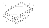
まず、本発明の第1の実施形態に係る画像表示装置について、説明する。図1は、本実施形態に係る画像表示装置の外観を示す概要図である。同図に示されるように、本実施形態に係る画像表示装置1は、画像を表示する表示領域を含んだ表示パネル2と、表示パネル2に接続されたフレキシブルプリント基板3と、フレキシブルプリント基板3に接続されたリジッド基板4と、を含んで構成されている。なお、リジッド基板4は、例えば接着剤や両面テープで表示パネル2に固定されてもよいし、画像表示装置1の筐体フレームにネジ等で固定されてもよい。
[First Embodiment]
First, the image display apparatus according to the first embodiment of the present invention will be described. FIG. 1 is a schematic diagram illustrating an appearance of the image display apparatus according to the present embodiment. As shown in the figure, an image display device 1 according to this embodiment includes a
さらに、表示パネル2は、発光素子である有機EL素子をそれぞれ含む複数の画素回路が行列状に形成されたガラス基板と、当該ガラス基板に貼り合わされて有機EL素子を封止する封止基板と、表示パネル2の表示領域部分が開口するように封止基板を囲んだ前面フレームFFと、その反対側からガラス基板を囲み、スナップフィットにより前面フレームFFに固定された裏面フレームBFと、を含んで構成されている。さらに、前面フレームFFの表示領域に対応する開口部分には偏光板PPが貼り合わされている。
Furthermore, the
ガラス基板上には、薄膜トランジスタ(TFT)が形成され、この薄膜トランジスタを介して有機EL素子の発光が制御されることによって、画素毎の表示制御が行われる。図2は、ガラス基板上に実装される画素回路の概略構成の一例を示す図である。同図に示されるように、画像表示装置1の表示領域内にはそれぞれ発光素子を備えた複数の画素回路10が行列状に配置されており、各画素回路10には、データ信号線DAT、点灯スイッチ制御線ILM、リセットスイッチ制御線RES、及び電源線PWRが接続される。データ信号線DATは、表示画面の上下方向(図2のy軸方向)に沿って延在し、表示画面の左右方向(図2のx軸方向)に沿って互いに並んで複数本配置してある。また、点灯スイッチ制御線ILM及びリセットスイッチ制御線RESは、いずれも表示画面の左右方向(図2のx軸方向)に沿って延在し、表示装置の上下方向(図2のy軸方向)にそって互いに並んで複数本配置してある。すなわち、x軸方向に一列に並んだ複数の画素回路10が1つの画素行Prowを構成し、同じ画素行Prowに属する各画素回路10に対しては、共通する点灯スイッチ制御線ILM及びリセットスイッチ制御線RESが接続される。また、y軸方向に一列に並んだ複数の画素回路10が1つの画素列Pcolを構成し、同じ画素列Pcolに属する各画素回路10に対しては、共通するデータ信号線DATが接続される。
A thin film transistor (TFT) is formed on the glass substrate, and display control for each pixel is performed by controlling light emission of the organic EL element through the thin film transistor. FIG. 2 is a diagram illustrating an example of a schematic configuration of a pixel circuit mounted on a glass substrate. As shown in the figure, a plurality of
さらに、図2に示されるように、電源線PWRは表示領域内において格子状に配置されている。すなわち、図中x軸方向及びy軸方向それぞれに互いに並んで複数本の電源線PWRが延在しており、x軸方向に延びる電源線PWRとy軸方向に延びる電源線PWRとは、その交点で電気的に接続されている。この電源線PWRを介して、各画素回路10内の発光素子を駆動するための電力が供給される。このように電源線PWRが格子状に配置されることによって、電源線PWRの電気抵抗に起因する、電源線PWRを介して各画素に供給される電圧の降下を抑えることができる。なお、x軸方向に延びる電源線PWRとy軸方向に延びる電源線PWRとは互いに同種の材料によって形成されてもよいし、異なる材料により形成されてもよい。また、各方向に延びる複数本の電源線PWRは、各画素行または各画素列に1対1に対応して配置されてもよいし、複数行の画素行または複数列の画素列ごとに間隔をおいて配置されてもよい。図2の例では、y軸方向に延びる電源線PWRは画素列ごとに1本配置され、x軸方向に延びる電源線PWRは2行の画素行ごとに1本配置されている。
Further, as shown in FIG. 2, the power supply lines PWR are arranged in a grid pattern in the display area. That is, a plurality of power supply lines PWR are extended side by side in the x-axis direction and the y-axis direction in the figure, and the power supply line PWR extending in the x-axis direction and the power supply line PWR extending in the y-axis direction are: Electrically connected at the intersection. Power for driving the light emitting elements in each
なお、図2においては3行3列の計9個の画素回路10のみが示されているが、実際には表示パネルを構成する画素数に応じた数の画素回路がガラス基板上に行列状に配置される。例えばデジタルスチルカメラ等に用いられる水平方向640画素、垂直方向480画素の解像度の表示パネルの場合、各画素は赤(R)、緑(G)、青(B)それぞれの色に対応する3つのサブ画素から構成され、各サブ画素に対応して画素回路10が形成される。したがって、縦方向に480行、横方向に640×3=1920列で計(480×640×3)個の画素回路10がガラス基板上に形成されることとなる。なお、以降の説明においては、1個の画素回路10によって構成されるサブ画素のそれぞれを、単に画素と表記する。
In FIG. 2, only nine
さらに、各データ信号線DATの一端はデータ信号出力回路12に、点灯スイッチ制御線ILM及びリセットスイッチ制御線RESの一端はいずれも走査回路14に、それぞれ接続される。なお、データ信号出力回路12及び走査回路14は、各画素回路10を構成するスイッチなどと同様に、ガラス基板上に多結晶シリコンTFT素子等を用いて形成されることとしてよい。あるいは、データ信号出力回路12や走査回路14は、ガラス基板上に搭載された1個又は複数個のドライバICチップなどによって構成されてもよいし、このようなドライバICチップと多結晶シリコンTFT素子等の回路素子との組み合わせによって構成されてもよい。また、電源線PWRは、その端部で複数本の主電源線Pmのいずれかに接続される。本実施形態では、電源線PWRを介して各画素に発光素子を発光させるための電圧を印加する主電源線Pmが、複数本ガラス基板上に配置される。主電源線Pmの配置については、後述する。
Further, one end of each data signal line DAT is connected to the data signal
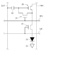
図3は、各画素回路10の構成例を示す回路図である。各画素回路10には、発光素子として有機EL素子20が設けられており、そのカソード端は共通電極22に接続される。共通電極22は、その電位が画像表示装置1において基準となる基準電位に設定された電極である。また、有機EL素子20のアノード端は、n型のTFTによって構成される点灯スイッチ24の一端に接続され、点灯スイッチ24の他端は、p型のTFTである駆動TFT26を介して電源線PWRに接続される。駆動TFT26及び点灯スイッチ24がともにオン状態になると、電源線PWRから共通電極22に向かって有機EL素子20内に電流が流れ、これによって有機EL素子20が発光する。
FIG. 3 is a circuit diagram illustrating a configuration example of each
さらに、点灯スイッチ24の他端と駆動TFT26のゲートとの間には、n型のTFTによって構成されるリセットスイッチ28が接続され、駆動TFT26のゲートにはさらに保持容量30の一端が接続される。そして、保持容量30の他端はデータ信号線DATに接続される。また、図2に示されるように、点灯スイッチ24のゲートは点灯スイッチ制御線ILMに、リセットスイッチ28のゲートはリセットスイッチ制御線RESに、それぞれ接続されている。これらの制御線からVH(高電圧)及びVL(低電圧)の二値の電圧レベルの制御信号が入力されることによって、各スイッチのオン/オフが切り替えられる。
Further, a
この図に示す画素回路10では、まずリセットスイッチ28及び点灯スイッチ24がオン状態になることによって、画素に設定された輝度情報のリセットが行われる。そして、データ信号線DATを介して当該画素を発光させようとする輝度情報に応じた電圧レベルの信号が入力され、その情報が保持容量30に保持される。その後、点灯スイッチ24がオン状態になるとともに、データ信号線DATを介して三角波などの時間とともに電圧レベルが上下する発光期間制御信号が入力されることによって、この発光期間制御信号が輝度情報に応じた閾値を下回る期間の間だけ、有機EL素子20が発光する。これにより、予め書き込まれた輝度情報に応じて発光期間の長短が変化することとなり、この発光期間の長短によって各画素の輝度が制御される。なお、本実施形態では、輝度情報の書き込みは画素行ごとに行われるが、この発光期間制御信号の入力は表示画面内の全画素に対して一斉に行われる。そのため、1フレーム期間のうちの同じタイミングで各画素が一斉に発光することになる。
In the
図4は、画像表示装置1における、表示パネル2の断面構造の一例を示す断面図である。この図4の例では、ある一つの画素を構成する有機EL素子20及びこれに接続されるTFTを含んだ部分の断面構造が示されている。なお、同図における上方向を向いた矢印は、光の放射方向を示している。
FIG. 4 is a cross-sectional view showing an example of the cross-sectional structure of the
図4に示されるように、表示パネル2を製造する際には、まずLTPS工程において、ガラス基板SUB1上に、多結晶シリコンを材料としたチャネル層FG、P−TEOSを材料としたゲート絶縁膜INS1、MoWを材料としたゲート配線SG、P−TEOSを材料としたCONT絶縁膜INS2、金属材料により形成されるソース/ドレイン配線AL、P−SiNを材料としたパッシベーション層PASを順に積層して、TFTを形成する。その後、パッシベーション層PASの上にTFT形成によって生じた段差を平坦化するための平坦化層OCを形成する。平坦化層OCは、窒化シリコンなどの無機膜や、アクリル樹脂、ポリイミド樹脂などの有機膜であってよい。次に、平坦化層OC上に反射層AMを形成する。反射層AMは、例えばMoW(Mo:80wt%、W:20wt%)とAlSi(Si:1.0wt%以下)の二層構造によって形成される。続いて、ITOからなる陽極ADを形成する。この陽極ADは、ソース/ドレイン配線ALと接続される。その後、LTPS工程の最後に、電極端部での陽極−陰極間のショートを防ぐためのSiNバンクSiL2を形成する。
As shown in FIG. 4, when the
次に、OLED工程において、RGBを打ち分けるための精密マスクを用いて有機EL層ELを形成し、表示領域全体を覆う形でIZOからなる透明陰極CDを形成する。透明陰極CDは薄膜化する必要があるため、隣接画素間の抵抗を小さくするように、さらに補助電極AUXを形成する。最後に、水分侵入を防ぐために乾燥剤を塗布した封止基板SUB2をN2環境下で封止して、表示パネルを製造する。 Next, in the OLED process, an organic EL layer EL is formed using a precision mask for separating RGB, and a transparent cathode CD made of IZO is formed so as to cover the entire display region. Since the transparent cathode CD needs to be thinned, an auxiliary electrode AUX is further formed so as to reduce the resistance between adjacent pixels. Finally, the display substrate is manufactured by sealing the sealing substrate SUB2 coated with a desiccant in order to prevent intrusion of moisture in an N 2 environment.
なお、ここでは画像表示装置1がトップエミッション型の有機EL表示装置であるものとして、その断面構造を説明したが、画像表示装置1はこれに限らずボトムエミッション型の有機EL表示装置であってもよい。 Here, the cross-sectional structure has been described on the assumption that the image display device 1 is a top emission type organic EL display device, but the image display device 1 is not limited to this and is a bottom emission type organic EL display device. Also good.
図5は、以上説明した画素回路10が行列状に配列することによってガラス基板SUB1上に形成された、表示領域SAの概要を示す概略平面図である。同図に示されるように、本実施形態では、表示領域SAは3個の部分領域A1〜A3に分割されている。すなわち、表示領域SAは、同じ画素列Pcolに属する画素が同じ部分領域に含まれるように、その上下方向(y軸方向)に沿って3個に分割されている。
FIG. 5 is a schematic plan view showing an outline of the display area SA formed on the glass substrate SUB1 by arranging the
そして、各部分領域A1,A2及びA3に対して、互いに独立に各画素の発光素子を発光させるための電力供給が行われる。具体的に、部分領域A1内の電源線PWRは主電源線Pm1に接続されており、部分領域A1内の各画素に対してはこの主電源線Pm1を介して電力が供給される。また、部分領域A2内の各画素に対しては主電源線Pm2を介して、部分領域A3内の各画素に対しては主電源線Pm3を介して、それぞれ電力供給が行われる。そして、これら主電源線Pm1,Pm2及びPm3は、互いに独立した電力供給路になっている。これにより、画面全体において画面内輝度傾斜を発生し難くすることができる。 Then, power is supplied to each of the partial areas A1, A2, and A3 so that the light emitting elements of the respective pixels emit light independently of each other. Specifically, the power supply line PWR in the partial area A1 is connected to the main power supply line Pm1, and power is supplied to each pixel in the partial area A1 through the main power supply line Pm1. Further, power is supplied to each pixel in the partial area A2 via the main power supply line Pm2, and each pixel in the partial area A3 is supplied via the main power supply line Pm3. The main power supply lines Pm1, Pm2, and Pm3 are independent power supply paths. Thereby, it is possible to make it difficult for the luminance gradient in the screen to occur in the entire screen.
さらに本実施形態では、これら主電源線Pm1,Pm2及びPm3のそれぞれが対応する部分領域に対して供給する電力は、互いに独立して制御される。したがって、各部分領域に供給される電力は、互いに異なる大きさにすることが可能になっている。図6は、このような制御を実現するために本実施形態に係る画像表示装置1が備える機能の一例を示す機能ブロック図である。同図に示されるように、画像表示装置1は、画像データ制御部32と、駆動回路制御部34と、領域画像情報取得部36と、電力制御部38と、電源出力部40と、を含んで構成される。これらの機能は、例えばフレキシブルプリント基板3やリジッド基板4に実装されたマイクロプロセッサ等が、予め所定の記憶領域に記憶されたプログラムを実行することによって実現されてよい。また、これらの機能の一部はデジタル回路やアナログ回路等によって実現されてもよい。
Furthermore, in the present embodiment, the power supplied to the corresponding partial regions by the main power supply lines Pm1, Pm2, and Pm3 is controlled independently of each other. Therefore, the electric power supplied to each partial area can be made different in magnitude. FIG. 6 is a functional block diagram illustrating an example of functions provided in the image display apparatus 1 according to the present embodiment in order to realize such control. As shown in the figure, the image display device 1 includes an image
画像データ制御部32は、外部から画像データ信号の入力を受け付けて、当該受け付けた画像データを表示パネル2に表示するための画像処理を実行する。駆動回路制御部34は、この画像データ制御部32が出力する画像データに関する信号を毎フレームごとに受け付けて、この画像データに応じた各画素の輝度情報を表示パネル2内のデータ信号出力回路12に供給する。
The image
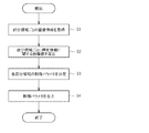
一方、領域画像情報取得部36及び電力制御部38は、画像データ制御部32から出力される画像データに関する情報を用いて、電源出力部40から表示パネル2に供給される電力の制御を行う。図7は、この制御の具体例を示すフロー図である。
On the other hand, the area image
図7の例では、領域画像情報取得部36は、画像データ制御部32から画像データに関する信号を受け付けて、図6に示す部分領域ごとに、当該部分領域に含まれる画像に関する情報を取得する(S1)。電力制御部38は、このS1で取得された部分領域ごとの画像に関する情報を用いて、部分領域ごとに画素の輝度情報に関する指標値を算出する(S2)。この指標値は、例えば各部分領域において所定の閾値以上の輝度で発光させるべき画素の数や、各画素の輝度を表す値の合計値など、対応する部分領域についてどの程度の明るさの画像を表示するかに関する値であってよい。
In the example of FIG. 7, the area image
続いて電力制御部38は、S2で算出した指標値に基づいて、各部分領域について出力されるべき電源電圧の値に対応する制御パラメタを決定する(S3)。この制御パラメタは、例えば0〜63までの6ビットの値によって表され、それぞれ5.00V〜10.0Vまでの電源電圧の値に対応づけられている。すなわち、ここでは制御パラメタの値0が5.00Vに、値1が5.08Vに、というように、各制御パラメタの値が0.08Vずつ異なる複数の電源電圧の値のいずれかに対応づけられている。電力制御部38は、このS3で決定した制御パラメタを電源出力部40に対して出力する(S4)。
Subsequently, the
電源出力部40は、電源回路等を含んで構成され、電力供給源(電池など)から供給される電力を、主電源線Pm1,Pm2及びPm3のそれぞれに対して出力する。ここで、電源出力部40は、電力制御部38が前述したS4の処理で出力する制御パラメタの値に応じて、主電源線Pm1,Pm2及びPm3のそれぞれに対して供給する電力を制御する。ここでは具体的に、電源出力部40は、各部分領域について算出された制御パラメタの値に対応する5.00V〜10.0Vまでの範囲のいずれかの電圧値に応じて、各主電源線Pmに対して印加する電圧を変化させる。こうして、各部分領域に対して、互いに異なる電圧で電力を供給することが可能となる。また、ここでは、各部分領域に対して印加する電圧を、当該部分領域内の発光画素数や発光量などの、当該部分領域に表示するべき画像に関する指標値に応じて変化させている。こうすれば、より電圧降下の影響が生じやすいと予想される部分領域に対して、高い電圧での電力供給を行うことで、画面内輝度傾斜の影響を軽減ができる。
The
なお、以上の説明においては、入力される画像データに応じて各部分領域に対して供給する電力を制御することとしたが、これに限らず、画像表示装置1は各部分領域の表示領域SA内の位置に応じて、当該部分領域に対して供給する電力の大きさを制御することとしてもよい。例えば電力制御部38は、表示領域SAの中心位置に近い部分領域ほど、より大きな電力を供給し、逆に表示領域SAの中心位置から離れた部分領域に対しては、より小さな電力を供給するように電源出力部40を制御してもよい。
In the above description, the power supplied to each partial area is controlled according to the input image data. However, the present invention is not limited to this, and the image display apparatus 1 displays the display area SA of each partial area. The magnitude of the electric power supplied to the partial area may be controlled according to the position inside. For example, the
具体例として、電源出力部40は、部分領域A2に対応する主電源線Pm2に対しては他の主電源線Pm1及びPm3より高い電圧を出力し、部分領域A1及びA3に対応する主電源線Pm1及びPm3に対しては、主電源線Pm2より低い電圧を出力してもよい。図8、図9A及び図9Bは、この場合における表示画面内の輝度について説明するための図である。図8は表示領域SAにおけるA−A’線及びB−B’線の位置を示しており、図9Aは、表示領域SA内の全画素を最大(100%)の輝度で点灯した際の、このA−A’線に沿った画素の輝度分布を示している。同様に、図9BはB−B’線に沿った画素の輝度分布を示している。なお、図9A及び図9Bの縦軸Lは輝度を示している。これらの図の例では、表示領域SAのx軸方向における中心を示す中心線の近傍で、輝度が高くなり、画面左右両端に近い位置では相対的に輝度が低くなる。こうすれば、閲覧者の注目を集めやすい画面中央近傍の部分領域A2における輝度を下げることなく、主電源線Pm1及びPm3に出力する電圧を下げて、消費電力を抑えることができる。
As a specific example, the
[第2実施形態]
次に、本発明の第2の実施形態に係る画像表示装置について、説明する。なお、本実施形態に係る画像表示装置に関して、第1実施形態と同様の構成や機能についてはその説明を省略し、以下では第1実施形態と異なる部分についてだけ説明する。また、第1実施形態と同様の構成要素については、同一の参照符号を用いて参照する。
[Second Embodiment]
Next, an image display apparatus according to the second embodiment of the present invention will be described. In addition, regarding the image display apparatus according to the present embodiment, descriptions of the same configurations and functions as those of the first embodiment are omitted, and only portions different from the first embodiment will be described below. In addition, the same reference numerals are used to refer to the same components as those in the first embodiment.
本実施形態では、表示領域SA内における部分領域の配置、及びこの部分領域の配置に対応する主電源線Pmの配置が第1実施形態とは異なっている。図10は、本実施形態における表示領域SA内の部分領域の配置を示す概略平面図である。同図に示されるように、本実施形態では、表示領域SAは3個の部分領域A4〜A6に分割されている。ここでは図5に示す第1実施形態の例とは異なり、同じ画素行Prowに属する画素が同じ部分領域に含まれるように、表示領域SAはその左右方向(x軸方向)に沿って3個に分割されている。 In the present embodiment, the arrangement of the partial areas in the display area SA and the arrangement of the main power supply lines Pm corresponding to the arrangement of the partial areas are different from those in the first embodiment. FIG. 10 is a schematic plan view showing the arrangement of partial areas in the display area SA in the present embodiment. As shown in the figure, in the present embodiment, the display area SA is divided into three partial areas A4 to A6. Here, unlike the example of the first embodiment shown in FIG. 5, there are three display areas SA along the horizontal direction (x-axis direction) so that pixels belonging to the same pixel row Prow are included in the same partial area. It is divided into
さらに、本実施形態では、各部分領域に対してそれぞれ複数の主電源線Pmから電力供給が行われる。すなわち、部分領域A4内の各画素に対しては2本の主電源線Pm4から、部分領域A5内の各画素に対しては2本の主電源線Pm5から、部分領域A6内の各画素に対しては2本の主電源線Pm6から、それぞれ電力供給が行われる。 Furthermore, in the present embodiment, power is supplied from each of the plurality of main power supply lines Pm to each partial region. That is, from the two main power supply lines Pm4 for each pixel in the partial area A4, to each pixel in the partial area A6 from the two main power supply lines Pm5 for each pixel in the partial area A5. On the other hand, power is supplied from the two main power supply lines Pm6.
これらの主電源線Pmを介して供給される電力の大きさは、第1実施形態において説明した例と同様に、対応する部分領域内に表示すべき画像の内容に応じて制御されることとしてもよい。あるいは、各部分領域の表示領域SA内における位置に応じて、各部分領域に供給される電力の大きさが制御されることとしてもよい。 As in the example described in the first embodiment, the magnitude of the power supplied via these main power supply lines Pm is controlled according to the content of the image to be displayed in the corresponding partial area. Also good. Alternatively, the magnitude of power supplied to each partial area may be controlled according to the position of each partial area in the display area SA.
図11A及び図11Bは、図10に示す本実施形態の部分領域の配置において、対応する各部分領域の位置に応じて出力電圧を制御した場合の輝度分布の一例を示している。なお、これらの図は図9A及び図9Bと同様に、図8に示すA−A’線及びB−B’線に沿った画素の輝度分布を示している。この図11A及び図11Bにおいては、電源出力部40は、表示領域SAの中心を含む部分領域A5に対応する主電源線Pm5に対しては、他の主電源線Pm4及びPm6より高い電圧を出力し、部分領域A4及びA6に対応する主電源線Pm4及びPm6に対しては、主電源線Pm5より低い電圧を出力することとしている。この場合、図11及び図11Bに示すように、表示領域SAのy軸方向の中心を示す中心線の近傍で輝度が高くなり、画面上下両端に近い位置では相対的に輝度が低くなっている。これにより、図9A及び図9Bの例と同様に、閲覧者の注目を集めやすい画面中央近傍の部分領域A5における輝度を下げることなく、主電源線Pm4及びPm6に出力する電圧を下げて、消費電力を抑えることができる。
11A and 11B show an example of the luminance distribution when the output voltage is controlled according to the position of each corresponding partial region in the arrangement of the partial regions of this embodiment shown in FIG. In addition, these figures show the luminance distribution of the pixels along the A-A ′ line and the B-B ′ line shown in FIG. 8, similarly to FIGS. 9A and 9B. 11A and 11B, the
[第3実施形態]
次に、本発明の第3の実施形態に係る画像表示装置について、説明する。なお、本実施形態に係る画像表示装置についても、表示領域SA内における部分領域の配置、及びこの部分領域の配置に対応する主電源線Pmの配置を除けば、他の実施形態と同様の構成を備えている。
[Third Embodiment]
Next, an image display apparatus according to a third embodiment of the present invention will be described. The image display apparatus according to the present embodiment also has the same configuration as the other embodiments except for the arrangement of the partial areas in the display area SA and the arrangement of the main power supply lines Pm corresponding to the arrangement of the partial areas. It has.
図12は、本実施形態における表示領域SA内の部分領域の配置を示す概略平面図である。同図に示されるように、本実施形態では、表示領域SAは縦3個、横3個で計9個の部分領域A7〜A15に分割されている。そして、部分領域A7〜A15のそれぞれに含まれる各画素に対して、互いに独立した主電源線Pm7〜Pm15を介して電力供給が行われる。 FIG. 12 is a schematic plan view showing the arrangement of partial areas in the display area SA in the present embodiment. As shown in the figure, in the present embodiment, the display area SA is divided into nine partial areas A7 to A15 in three vertical and three horizontal areas. Then, power is supplied to each pixel included in each of the partial areas A7 to A15 via the main power supply lines Pm7 to Pm15 independent of each other.
これらの主電源線Pmを介して供給される電力の大きさは、第1及び第2実施形態において説明した例と同様に、対応する部分領域内に表示すべき画像に応じて制御されることとしてもよい。あるいは、各部分領域の表示領域SA内における位置に応じて、各部分領域に供給される電力の大きさが制御されることとしてもよい。 The magnitude of the power supplied via these main power supply lines Pm is controlled according to the image to be displayed in the corresponding partial area, as in the examples described in the first and second embodiments. It is good. Alternatively, the magnitude of power supplied to each partial area may be controlled according to the position of each partial area in the display area SA.
具体例として、本実施形態に係る画像表示装置は、表示領域SAの中心を含む部分領域A11に対応する主電源線Pm11に対しては、他の主電源線Pmと比較して相対的に高い電圧を出力することとしてもよい。さらに、その重心位置がより表示領域SAの中心より離れた部分領域A7,A9,A13及びA15のそれぞれに対応する主電源線Pm7,Pm9,Pm13及びPm15に対して出力する電圧は、相対的に表示領域SAの中心位置に近い部分領域A8,A10,A12及びA14のそれぞれに対応する主電源線Pm8,Pm10,Pm12及びPm14に対して出力する電圧より低くすることとしてもよい。この場合、図8に示すA−A’線及びB−B’線に沿った画素の輝度分布は、それぞれ図9A及び図11Bに示したものと同様のものになる。これにより、閲覧者の注目を集めやすい画面中央近傍の部分領域A11における輝度を下げることなく、他の主電源線Pmに出力する電圧を下げて、消費電力を抑えることができる。 As a specific example, the image display device according to the present embodiment is relatively high with respect to the main power supply line Pm11 corresponding to the partial area A11 including the center of the display area SA as compared with the other main power supply lines Pm. It is good also as outputting a voltage. Furthermore, the voltages output to the main power supply lines Pm7, Pm9, Pm13, and Pm15 corresponding to the partial areas A7, A9, A13, and A15 whose center of gravity is further away from the center of the display area SA are relatively The voltage may be lower than the voltage output to the main power supply lines Pm8, Pm10, Pm12, and Pm14 corresponding to the partial areas A8, A10, A12, and A14 close to the center position of the display area SA. In this case, the luminance distributions of the pixels along the A-A ′ line and the B-B ′ line shown in FIG. 8 are the same as those shown in FIGS. 9A and 11B, respectively. Thereby, the voltage output to the other main power supply line Pm can be lowered without lowering the luminance in the partial area A11 near the center of the screen where the viewer's attention is likely to be gathered, thereby reducing the power consumption.
なお、本実施形態では、これまで説明した他の実施形態と異なり、一部の部分領域(具体的には部分領域A11)は表示領域SAの外周に接していない。そのため、表示領域SAの外周に沿って配置した主電源線Pmだけで各部分領域への電力供給を行うことができず、部分領域A11に電力供給を行うための主電源線Pm11は他の部分領域内を通るように配置する必要がある。この場合でも、例えば図4の断面図におけるガラス基板SUB1のすぐ上の位置など、画素回路10が形成される層とガラス基板SUB1との間の層に主電源線Pmを形成することによって、他の部分領域内の画素回路10と干渉しないように、表示領域SA内に主電源線Pmを配置することができる。
In the present embodiment, unlike the other embodiments described so far, a part of the partial area (specifically, the partial area A11) is not in contact with the outer periphery of the display area SA. Therefore, it is impossible to supply power to each partial area only with the main power supply line Pm arranged along the outer periphery of the display area SA, and the main power supply line Pm11 for supplying power to the partial area A11 has other parts. It is necessary to arrange to pass through the area. Even in this case, for example, by forming the main power supply line Pm in a layer between the layer on which the
以上説明した本発明の実施の形態に係る画像表示装置によれば、発光素子を発光させるために各画素に対して供給される電力を、表示領域内の位置に応じて制御することができる。これによって、画面内の位置に依存して輝度が変化する画面内輝度傾斜を抑えたり、閲覧者が感じる見かけの輝度を下げずに各画素内の発光素子を発光させるために必要な電力を抑えたりすることができる。 According to the image display device according to the embodiment of the present invention described above, it is possible to control the power supplied to each pixel for causing the light emitting element to emit light according to the position in the display region. As a result, the power required to light up the light emitting elements in each pixel without reducing the brightness gradient in the screen where the brightness changes depending on the position in the screen, or reducing the apparent brightness felt by the viewer. Can be.
なお、本発明の実施の形態に係る画像表示装置は、パソコン用ディスプレイ、TV放送受信用ディスプレイ、公告表示用ディスプレイ等の各種の情報表示用の表示装置として採用できる。また、デジタルスチルカメラ、ビデオカメラ、カーナビゲーションシステム、カーオーディオ、ゲーム機器、携帯情報端末など、各種の電子機器の表示部として利用することも可能である。 The image display device according to the embodiment of the present invention can be employed as a display device for displaying various information such as a personal computer display, a TV broadcast receiving display, and a notification display. Further, it can be used as a display unit of various electronic devices such as a digital still camera, a video camera, a car navigation system, a car audio, a game device, and a portable information terminal.
[変形例]
以下、本発明の実施形態に係る画像表示装置のいくつかの変形例について、説明する。
[Modification]
Hereinafter, some modifications of the image display device according to the embodiment of the present invention will be described.
まず、本発明の実施形態に係る画像表示装置において、他の部分領域とは独立に電力供給が行われる一つの部分領域は、さらに互いに分離した複数の小領域から構成されることとしてもよい。具体例として、x軸方向又はy軸方向に沿って表示領域SAを複数の小領域に分割し、これら小領域のうち、一つおきに配置された複数の小領域からなる第1の部分領域に対しては第1の主電源線Pmから電力を供給し、それ以外の複数の小領域からなる第2の部分領域に対しては第2の主電源線Pmから電力を供給することとしてもよい。この場合にも、表示領域SAを複数の部分領域に分割し、そのそれぞれに対して互いに独立に電力供給を行うことができるので、表示領域SA内の各画素が一斉に点灯する際に生じる画面内輝度傾斜の影響を低減することができる。さらに、このように各部分領域が画面全体に分散して配置される小領域から構成されることによって、例えば表示領域SAの一部の範囲に発光対象の画素が集中した場合にも、当該範囲が複数の部分領域にまたがる可能性が高くなり、画面内輝度傾斜の影響を低減しやすくなる。 First, in the image display device according to the embodiment of the present invention, one partial region to which power is supplied independently of other partial regions may be configured of a plurality of small regions separated from each other. As a specific example, the display area SA is divided into a plurality of small areas along the x-axis direction or the y-axis direction, and among these small areas, a first partial area composed of a plurality of small areas arranged alternately. For example, power is supplied from the first main power supply line Pm, and power is supplied from the second main power supply line Pm to the second partial region composed of a plurality of other small regions. Good. Also in this case, since the display area SA can be divided into a plurality of partial areas, and power can be supplied to each of them independently, the screen generated when the pixels in the display area SA are lit simultaneously. The influence of the inner luminance gradient can be reduced. In addition, since each partial area is composed of small areas distributed over the entire screen in this way, for example, even when pixels targeted for light emission are concentrated in a partial range of the display area SA, Is likely to extend over a plurality of partial areas, and the influence of the in-screen luminance gradient is easily reduced.
また、部分領域の少なくとも一部は、隣接する他の部分領域と重なり合う領域を含むように配置されてもよい。この場合、他の部分領域との重複領域においては、それぞれ独立した主電源線Pmから電力供給を受ける画素行Prow又は画素列Pcolが互い違いに配置されるなど、それぞれ独立した主電源線Pmから電力供給を受ける画素が混在することになる。こうすれば、互いに隣接する部分領域の境界近傍で、本来同じ輝度で発光するべき画素の輝度が急激に変化してしまう現象を抑え、部分領域の境界を目立たないようにすることができる。 Further, at least a part of the partial area may be arranged to include an area overlapping with another adjacent partial area. In this case, in the overlapping area with the other partial areas, the pixel rows Prow or the pixel columns Pcol that receive power supply from the independent main power supply lines Pm are alternately arranged. Pixels to be supplied are mixed. By so doing, it is possible to suppress a phenomenon in which the luminance of pixels that should originally emit light with the same luminance is rapidly changed in the vicinity of the boundary between the partial regions adjacent to each other, thereby making the boundary between the partial regions inconspicuous.
また、各主電源線Pmに対して供給する電力の大きさを制御する電力制御部38は、各部分領域の位置や各部分領域内に表示する画像に関する情報だけでなく、他の条件に応じて電力供給の制御を行ってもよい。すなわち、例えば電力制御部38は、画像表示装置1の外部環境(外光の明るさなど)に応じて各主電源線Pmに供給する電力の大きさを変化させてもよい。具体例として、電力制御部38は、外光の明るさに関する情報を光センサの出力などによって定期的に取得し、当該取得した情報に応じて複数の表示モードの中から表示モードを選択する。そして、選択した表示モードに応じて、表示画面全体の明るさを変化させるように、各主電源線Pmに供給する電力の大きさを変化させる。このとき、電力制御部38は取得した情報に応じて全ての主電源線Pmの供給電力を共通して変化させてもよいし、各主電源線Pmの供給電力を独立に変化させてもよい。例えば、表示画面に対して互いに異なる方向に配置された複数の光センサそれぞれの出力に応じて、複数の部分領域のそれぞれに対して互いに異なる電圧値で電力供給を行ってもよい。
In addition, the
また、電力制御部38は、表示されるアプリケーションコンテンツの内容に応じて、各主電源線Pmに対する供給電力を変化させてもよい。具体的には、例えばメニュー画面を表示する場合と写真画像を表示する場合とで供給電力を変更することとしてもよい。この場合、例えば電力制御部38は、画像データ制御部32から表示画像の種別に関する情報を取得し、この取得した情報に応じて供給電力を制御する。
Further, the
さらに、電力制御部38は、継続動作時間や過去に表示した画像の内容に応じて各主電源線Pmに対する供給電力を変化させてもよい。具体例として、電力制御部38は、一定時間画像内容に変化がない部分領域が存在する場合に、当該部分領域に対して供給する電力を抑制する制御を行う。このような制御を実現するために、例えば電力制御部38は、所定時間おきに部分領域ごとの画像内容に関する統計情報を算出し、この統計情報が前回算出時から所定の閾値以上変化している場合に、画像に変化があったと判定し、その変化のタイミングを示す情報(例えば時刻情報)をメモリの所定領域に書き込む。そして、このタイミングを示す情報を定期的に参照することによって、各部分領域に表示する画像内容が最後に変化してから所定時間が経過したか否かを判定する。このような制御によれば、例えばメニュー表示などによって表示画面内の所定の部分領域に同じ画像が表示され続けている場合に、当該部分領域だけに供給する電力を抑えることによって、他の領域の輝度を下げることなく、当該部分領域の焼き付けを生じにくくするよう制御できる。
Furthermore, the
なお、以上説明した電力制御部38が各主電源線Pmへの供給電力を決定するために用いる各種の条件は、組み合わせて用いられることとしてもよい。例えば電力制御部38は、各条件によって決まる評価値を合算して算出される制御パラメタに応じて、各主電源線Pmに印加する電圧を変化させてもよい。また、電力制御部38は、外光が所定の閾値以上の明るさのときには各部分領域の表示領域SA内における位置に応じた電力制御(例えば画面中央近傍の部分領域の輝度を高める制御)を実行し、外光が所定の閾値未満の明るさの場合にはこのような制御を実行せずに画面全体を均一の輝度で発光させることとしてもよい。
Various conditions used by the
なお、以上の説明においては発光素子として有機EL素子を用いることとしたが、これに限らず、本発明の実施の形態に係る画像表示装置は、例えば無機EL素子やFED(Field-Emission Device)など、入力される電流や電圧に依存して輝度が変化する各種の発光素子を用いた画像表示装置であってよい。また、画素回路の構成や画素の発光制御方法も、以上説明したものに限らず、他の構成や方法であってもよい。 In the above description, the organic EL element is used as the light emitting element. However, the present invention is not limited to this, and the image display device according to the embodiment of the present invention may be, for example, an inorganic EL element or FED (Field-Emission Device). For example, an image display apparatus using various light emitting elements whose luminance changes depending on input current or voltage may be used. Further, the configuration of the pixel circuit and the light emission control method of the pixel are not limited to those described above, and other configurations and methods may be used.
1 画像表示装置、2 表示パネル、3 フレキシブルプリント基板、4 リジッド基板、10 画素回路、12 データ信号出力回路、14 走査回路、20 有機EL素子、22 共通電極、24 点灯スイッチ、26 駆動TFT、28 リセットスイッチ、30 保持容量、32 画像データ制御部、34 駆動回路制御部、36 領域画像情報取得部、38 電力制御部、40 電源出力部、DAT データ信号線、ILM 点灯スイッチ制御線、Pm 主電源線、PWR 電源線、RES リセットスイッチ制御線、SA 表示領域。 DESCRIPTION OF SYMBOLS 1 Image display apparatus, 2 Display panel, 3 Flexible printed circuit board, 4 Rigid board, 10 Pixel circuit, 12 Data signal output circuit, 14 Scan circuit, 20 Organic EL element, 22 Common electrode, 24 Lighting switch, 26 Driving TFT, 28 Reset switch, 30 holding capacity, 32 image data control unit, 34 drive circuit control unit, 36 area image information acquisition unit, 38 power control unit, 40 power output unit, DAT data signal line, ILM lighting switch control line, Pm main power source Line, PWR power line, RES reset switch control line, SA display area.
Claims (8)
前記表示領域を分割してなる複数の部分領域のそれぞれに対して、当該部分領域に属する各画素の発光素子を発光させるための電力を、他の部分領域とは独立に供給する電力供給路と、
前記電力供給路が前記各部分領域に対して供給する電力を制御する電力制御部と、
を含むことを特徴とする画像表示装置。 In an image display device that displays an image by causing a light emitting element included in each of a plurality of pixels arranged in a display region to emit light,
A power supply path that supplies, to each of a plurality of partial areas obtained by dividing the display area, power for causing the light emitting elements of each pixel belonging to the partial area to emit light independently of the other partial areas; ,
A power control unit for controlling the power supplied to the partial areas by the power supply path;
An image display device comprising:
前記電力制御部は、前記各部分領域の位置に応じて、当該部分領域に対して前記電力供給路が供給する電力を制御する
ことを特徴とする画像表示装置。 The image display device according to claim 1,
The power display unit controls the power supplied from the power supply path to the partial area according to the position of each partial area.
前記電力制御部は、前記各部分領域の前記表示領域中心からの距離に応じて、当該部分領域に対して前記電力供給路が供給する電力を制御する
ことを特徴とする画像表示装置。 The image display device according to claim 2,
The power control unit controls power supplied from the power supply path to the partial area according to a distance from the center of the display area of each partial area.
前記電力制御部は、前記各部分領域内に表示する画像の内容に応じて、当該部分領域に対して前記電力供給路が供給する電力を制御する
ことを特徴とする画像表示装置。 The image display device according to claim 1,
The image display apparatus according to claim 1, wherein the power control unit controls the power supplied from the power supply path to the partial area according to the content of the image displayed in the partial area.
前記電力制御部は、前記各部分領域内に表示する画像の明るさを示す指標値に応じて、当該部分領域に対して前記電力供給路が供給する電力を制御する
ことを特徴とする画像表示装置。 The image display device according to claim 4.
The power control unit controls power supplied from the power supply path to the partial area according to an index value indicating brightness of an image displayed in the partial area. apparatus.
前記部分領域の少なくとも一部は、隣接する他の部分領域と重なり合う領域を含んでいる
ことを特徴とする画像表示装置。 The image display device according to claim 1,
At least a part of the partial area includes an area that overlaps with another adjacent partial area.
前記部分領域の少なくとも一部は、前記表示領域内において互いに分離した複数の小領域から構成される
ことを特徴とする画像表示装置。 The image display device according to claim 1,
At least a part of the partial area includes a plurality of small areas separated from each other in the display area.
前記発光素子は、有機エレクトロルミネセンス素子であって、
前記電力供給路から供給される電流を前記有機エレクトロルミネセンス素子に流すことにより、当該有機エレクトロルミネセンス素子が発光する
ことを特徴とする画像表示装置。 The image display device according to claim 1,
The light emitting element is an organic electroluminescent element,
The organic electroluminescent element emits light by causing a current supplied from the power supply path to flow through the organic electroluminescent element.
Priority Applications (2)
| Application Number | Priority Date | Filing Date | Title |
|---|---|---|---|
| JP2009004590A JP2010164619A (en) | 2009-01-13 | 2009-01-13 | Image display device |
| US12/685,765 US20100177086A1 (en) | 2009-01-13 | 2010-01-12 | Image display device |
Applications Claiming Priority (1)
| Application Number | Priority Date | Filing Date | Title |
|---|---|---|---|
| JP2009004590A JP2010164619A (en) | 2009-01-13 | 2009-01-13 | Image display device |
Publications (1)
| Publication Number | Publication Date |
|---|---|
| JP2010164619A true JP2010164619A (en) | 2010-07-29 |
Family
ID=42318728
Family Applications (1)
| Application Number | Title | Priority Date | Filing Date |
|---|---|---|---|
| JP2009004590A Pending JP2010164619A (en) | 2009-01-13 | 2009-01-13 | Image display device |
Country Status (2)
| Country | Link |
|---|---|
| US (1) | US20100177086A1 (en) |
| JP (1) | JP2010164619A (en) |
Cited By (4)
| Publication number | Priority date | Publication date | Assignee | Title |
|---|---|---|---|---|
| JP2014130317A (en) * | 2012-12-27 | 2014-07-10 | Lg Display Co Ltd | Organic light emitting display |
| KR20160011202A (en) * | 2013-05-17 | 2016-01-29 | 탈레스 | Electro-optical device having a large pixel matrix |
| US11521535B2 (en) | 2016-08-26 | 2022-12-06 | Samsung Electronics Co., Ltd. | Display device and driving method therefor |
| KR20230148135A (en) * | 2016-06-17 | 2023-10-24 | 삼성디스플레이 주식회사 | Display panel, and electronic apparatus including the same |
Families Citing this family (16)
| Publication number | Priority date | Publication date | Assignee | Title |
|---|---|---|---|---|
| TWI491034B (en) * | 2010-04-21 | 2015-07-01 | Au Optronics Corp | Organic light emitting diode display |
| KR20140116659A (en) * | 2013-03-25 | 2014-10-06 | 삼성디스플레이 주식회사 | Organic Light Emitting Display |
| CN104036721B (en) * | 2014-05-15 | 2017-01-18 | 京东方科技集团股份有限公司 | Organic-light-emitting-diode display panel, and driving method and display device thereof |
| CN104809988B (en) * | 2015-05-18 | 2016-06-29 | 京东方科技集团股份有限公司 | A kind of OLED array and display floater, display device |
| CN109155115B (en) * | 2016-05-23 | 2020-12-08 | 堺显示器制品株式会社 | display device |
| CN107301843A (en) * | 2017-08-28 | 2017-10-27 | 深圳市华星光电半导体显示技术有限公司 | The power configuration structure and collocation method of top emitting AMOLED panel |
| CN107994056A (en) * | 2017-11-21 | 2018-05-04 | 武汉华星光电半导体显示技术有限公司 | Display panel and the display device with the display panel |
| US10325976B2 (en) | 2017-11-21 | 2019-06-18 | Wuhan China Star Optoelectronics Semiconductor Display Technology Co., Ltd. | Display panel and display device thereof |
| CN108470540B (en) * | 2018-06-21 | 2020-05-15 | 京东方科技集团股份有限公司 | A display panel, a driving method thereof, and a display device |
| US11042062B2 (en) * | 2018-10-04 | 2021-06-22 | Innolux Corporation | Electronic device |
| CN111007917A (en) * | 2018-10-04 | 2020-04-14 | 群创光电股份有限公司 | electronic device |
| KR102771185B1 (en) * | 2019-07-12 | 2025-02-21 | 삼성디스플레이 주식회사 | Backlight unit and display device including the same |
| CN110675819A (en) * | 2019-09-02 | 2020-01-10 | 深圳市华星光电半导体显示技术有限公司 | Connecting circuit of display panel light-emitting device |
| KR102709918B1 (en) * | 2019-12-18 | 2024-09-27 | 삼성디스플레이 주식회사 | Display device and driving method thereof |
| CN112086069B (en) * | 2020-09-29 | 2021-11-23 | Tcl华星光电技术有限公司 | Partition display structure, display panel and organic light emitting diode display panel |
| US11984073B2 (en) * | 2020-09-29 | 2024-05-14 | Tcl China Star Optoelectronics Technology Co., Ltd. | Partitioned display structure, display panel, and organic light-emitting diode display panel |
Family Cites Families (5)
| Publication number | Priority date | Publication date | Assignee | Title |
|---|---|---|---|---|
| JP3025251B2 (en) * | 1997-12-27 | 2000-03-27 | キヤノン株式会社 | Image display device and driving method of image display device |
| US7274363B2 (en) * | 2001-12-28 | 2007-09-25 | Pioneer Corporation | Panel display driving device and driving method |
| KR20060122476A (en) * | 2005-05-27 | 2006-11-30 | 삼성에스디아이 주식회사 | Electronic emission display device and driving method thereof |
| KR20070043543A (en) * | 2005-10-21 | 2007-04-25 | 삼성에스디아이 주식회사 | Electronic emission display device and control method thereof |
| JP5196744B2 (en) * | 2006-06-30 | 2013-05-15 | キヤノン株式会社 | Active matrix display device |
-
2009
- 2009-01-13 JP JP2009004590A patent/JP2010164619A/en active Pending
-
2010
- 2010-01-12 US US12/685,765 patent/US20100177086A1/en not_active Abandoned
Cited By (8)
| Publication number | Priority date | Publication date | Assignee | Title |
|---|---|---|---|---|
| JP2014130317A (en) * | 2012-12-27 | 2014-07-10 | Lg Display Co Ltd | Organic light emitting display |
| US9576522B2 (en) | 2012-12-27 | 2017-02-21 | Lg Display Co., Ltd. | Organic light emitting display |
| KR20160011202A (en) * | 2013-05-17 | 2016-01-29 | 탈레스 | Electro-optical device having a large pixel matrix |
| JP2016520872A (en) * | 2013-05-17 | 2016-07-14 | タレス | Electro-optical device with large pixel matrix |
| KR102178608B1 (en) | 2013-05-17 | 2020-11-13 | 탈레스 | Electro-optical device having a large pixel matrix |
| KR20230148135A (en) * | 2016-06-17 | 2023-10-24 | 삼성디스플레이 주식회사 | Display panel, and electronic apparatus including the same |
| KR102716507B1 (en) | 2016-06-17 | 2024-10-14 | 삼성디스플레이 주식회사 | Display panel, and electronic apparatus including the same |
| US11521535B2 (en) | 2016-08-26 | 2022-12-06 | Samsung Electronics Co., Ltd. | Display device and driving method therefor |
Also Published As
| Publication number | Publication date |
|---|---|
| US20100177086A1 (en) | 2010-07-15 |
Similar Documents
| Publication | Publication Date | Title |
|---|---|---|
| JP2010164619A (en) | Image display device | |
| CN113971935B (en) | Display device and terminal device | |
| US10304388B2 (en) | Organic light emitting display device | |
| JP5310372B2 (en) | Display device, luminance degradation correction method, and electronic device | |
| US8816997B2 (en) | Image display device | |
| CN107871765A (en) | display with power grid | |
| JP5346520B2 (en) | Image display device | |
| JP5364227B2 (en) | Display device with reading function and electronic device using the same | |
| KR102568932B1 (en) | Electroluminescence display | |
| KR20180062048A (en) | Electro-luminecense display apparatus | |
| US9263510B2 (en) | EL display device | |
| CN110556075B (en) | Display device and method of controlling the same | |
| JP2022021644A (en) | Display | |
| JP2019012621A (en) | Electro-optical device and electronic apparatus | |
| US20200249815A1 (en) | Display device and method for controlling display device | |
| US12542090B2 (en) | Display apparatus and vehicle | |
| CN117529147A (en) | Display substrate and display device | |
| JP5617319B2 (en) | Display device and electronic device | |
| JP4122949B2 (en) | Electro-optical device, active matrix substrate, and electronic apparatus | |
| KR20220096033A (en) | Display panel and display device | |
| KR20140080734A (en) | Organic light emitting display device | |
| CN221598581U (en) | Display panel and display device including the same | |
| JP2004087302A (en) | Electro-optical devices and electronic equipment | |
| US20260026151A1 (en) | Display device and electronic device including the same | |
| JP2008083483A (en) | Electrooptical device and driving method thereof, and electronic equipment |