JP2010102892A - Method and device for producing organic el display panel - Google Patents
Method and device for producing organic el display panel Download PDFInfo
- Publication number
- JP2010102892A JP2010102892A JP2008272131A JP2008272131A JP2010102892A JP 2010102892 A JP2010102892 A JP 2010102892A JP 2008272131 A JP2008272131 A JP 2008272131A JP 2008272131 A JP2008272131 A JP 2008272131A JP 2010102892 A JP2010102892 A JP 2010102892A
- Authority
- JP
- Japan
- Prior art keywords
- organic
- area
- coating liquid
- display panel
- partitioned
- Prior art date
- Legal status (The legal status is an assumption and is not a legal conclusion. Google has not performed a legal analysis and makes no representation as to the accuracy of the status listed.)
- Pending
Links
Images


Landscapes
- Coating Apparatus (AREA)
- Electroluminescent Light Sources (AREA)
Abstract
【課題】 バンクで囲まれた区画領域内に有機EL塗布液を吐出して有機化合物層を形成して有機EL表示パネルを製造する方法において、バンク形成時のパターニング誤差による区画領域内の面積変動により、有機化合物層の層厚が設計値からずれてしまう。特に、1枚の基板から複数枚の有機EL表示パネルを製造する量産時には大きな問題である。
【解決手段】 事前に区画領域それぞれの面積を取得し、取得した面積に応じて有機EL塗布液の量を制御しながら区画領域内に前記塗布液を吐出することにより、有機化合物層の層厚のずれを低減する。
【選択図】 図1PROBLEM TO BE SOLVED: To produce an organic EL display panel by ejecting an organic EL coating liquid into a partition area surrounded by a bank to form an organic compound display panel, and to change the area in the partition area due to a patterning error at the time of bank formation. As a result, the layer thickness of the organic compound layer deviates from the design value. In particular, this is a serious problem during mass production in which a plurality of organic EL display panels are manufactured from a single substrate.
The layer thickness of an organic compound layer is obtained by acquiring the area of each partition region in advance and discharging the coating solution into the partition region while controlling the amount of the organic EL coating solution according to the acquired area. Reduce the deviation.
[Selection] Figure 1
Description
本発明は、有機EL表示パネルの製造方法および装置に関するものである。 The present invention relates to a method and apparatus for manufacturing an organic EL display panel.
有機EL素子は、EL発光性能を持つ、有機低分子あるいは有機高分子からなる有機化合物層を有する素子であり、自己発光のため広い視野角性能を有し、また耐衝撃性に優れるなど、表示素子として理想的な特長を有している。このため、有機EL素子を複数配置した有機EL表示パネルの実用化に向け、各種の分野において研究開発が精力的に進められている。 An organic EL element is an element having an EL compound and an organic compound layer composed of an organic low molecule or organic polymer, has a wide viewing angle performance due to self-emission, and has excellent impact resistance. It has ideal characteristics as an element. For this reason, research and development has been vigorously advanced in various fields for practical use of an organic EL display panel in which a plurality of organic EL elements are arranged.
有機化合物層の製造方法として、真空蒸着法、印刷法、インクジェット法、ディスペンス法などが広く研究開発されている。 As a method for producing an organic compound layer, a vacuum deposition method, a printing method, an ink jet method, a dispensing method, and the like have been widely researched and developed.
この中でも特に、インクジェット法(特許文献1)やディスペンス法(特許文献2)は有機化合物の材料利用効率に優れ、量産に適した方法である。これらの溶媒に有機化合物材料を溶解した有機EL塗布液を塗布する製造方法において、有機EL塗布液を塗り分ける目的で、塗布領域をバンク(隔壁)で区画する構造が用いられている。 Among these, the inkjet method (Patent Document 1) and the dispensing method (Patent Document 2) are excellent in material utilization efficiency of organic compounds and are suitable for mass production. In a manufacturing method in which an organic EL coating solution in which an organic compound material is dissolved in these solvents is applied, a structure in which a coating region is partitioned by banks (partitions) is used for the purpose of coating the organic EL coating solution separately.
また、製造コスト低減を目的に、1枚の大判基板に複数の有機EL表示パネルを形成した後、基板を分割して有機EL表示パネルを生産する方法が用いられる。これにより、1枚の大判基板から、複数の表示パネルを効率良く生産することができる。
高精細の小型パネルの場合、バンクによって区画される領域(以下、区画領域と表記する)の幅は70μm以下、バンクの幅は10μm以下、と非常に微細なパターンを有する。さらに、区画領域内に形成する有機化合物層の層厚が薄いため、有機EL塗布液の塗布量はごく微量である。これらの理由から、バンクをパターニングする時の露光装置アライメント精度や感光性レジストのエッチング精度に起因するパターン形成誤差、すなわち区画領域の面積変動が無視できなくなる。現在、一般的に表示パネルの製造に用いられている、露光装置の精度や感光性レジストの性能では、設計通りにパターニングすることは難しく、平均すると設計パターンから1〜1.5μmの誤差ができてしまう。 In the case of a high-definition small panel, the width of a region partitioned by a bank (hereinafter referred to as a partitioned region) is 70 μm or less and the bank has a very fine pattern of 10 μm or less. Furthermore, since the organic compound layer formed in the partition region is thin, the coating amount of the organic EL coating solution is very small. For these reasons, pattern formation errors due to the alignment accuracy of the exposure apparatus when patterning the bank and the etching accuracy of the photosensitive resist, that is, variations in the area of the partition region cannot be ignored. Currently, it is difficult to perform patterning as designed because of the accuracy of the exposure apparatus and the performance of the photosensitive resist, which are generally used in the manufacture of display panels. On average, an error of 1 to 1.5 μm can be generated from the design pattern. End up.
つまり、インクジェット法等により区画領域内に有機EL塗布液を塗布する際、設計した面積に合わせて吐出量を一定に制御すると、パターニングにより区画領域の面積が変動するため、溶媒の揮発後に形成される有機化合物層の層厚は設計値からずれてしまう。 In other words, when the organic EL coating liquid is applied to the partition area by an inkjet method or the like, if the discharge amount is controlled to be constant according to the designed area, the area of the partition area varies due to patterning. The thickness of the organic compound layer deviates from the design value.
例えば、バンク幅が5μm、幅(画素幅に等しい)が27μmのストライプ状の区画領域を有する3インチVGAパネルを形成する場合を考える。バンクを構成する感光性レジストのパターン形成誤差により、バンク幅が片側0.5μmずつ変動した時、固形分濃度2%の塗布液を一定の液量で塗布すると溶媒揮発後の有機化合物層の層厚は約5%変動してしまう。 For example, consider a case where a 3-inch VGA panel having a striped partition region having a bank width of 5 μm and a width (equal to the pixel width) of 27 μm is formed. When the bank width fluctuates by 0.5 μm on one side due to pattern formation errors of the photosensitive resist that constitutes the bank, the organic compound layer after volatilization of the solvent is applied when a coating solution with a solid content concentration of 2% is applied. The thickness will vary by about 5%.
人の目でみて輝度むらのない表示パネルを実現するためには、有機化合物層の層厚誤差は、表示パネル全体で設計値の3%以下に抑えなければならない。前述したように、区画領域ごとに有機化合物層の膜厚が設計値からずれると、表示パネルの輝度むらという製品不良の原因となり、生産歩留まりを低下させる。 In order to realize a display panel having no luminance unevenness with human eyes, the layer thickness error of the organic compound layer must be suppressed to 3% or less of the design value for the entire display panel. As described above, when the film thickness of the organic compound layer deviates from the design value for each partition region, it causes a product defect such as luminance unevenness of the display panel, and decreases the production yield.
本発明は、上記の課題を解決する為に、基板面内に電極の間に配置された有機化合物層を含む有機EL素子を有し、前記有機化合物層は有機化合物材料を溶媒に溶かした塗布液を区画された領域内に塗布して形成される有機EL表示パネルを、1枚の基板から複数形成する有機EL表示パネルの製造方法であって、前記区画された領域それぞれの面積を取得する工程と、前記取得された面積に応じて前記塗布液の量あるいは濃度を制御しながら、前記区画された領域内に前記塗布液を吐出する工程と、を有することを特徴とする。 In order to solve the above-mentioned problems, the present invention has an organic EL element including an organic compound layer disposed between electrodes in a substrate surface, and the organic compound layer is an application in which an organic compound material is dissolved in a solvent. A method of manufacturing an organic EL display panel in which a plurality of organic EL display panels formed by applying a liquid in a partitioned area are formed from a single substrate, and the area of each partitioned area is acquired. And a step of discharging the coating liquid into the partitioned region while controlling the amount or concentration of the coating liquid according to the acquired area.
また、塗布液を、基板面内の区画された領域内に塗布する塗布装置であって、前記基板面内の一部の区画された領域の画像を取得する手段と、前記取得した画像から前記一部分の区画された領域それぞれの面積を算出する手段と、前記算出した基板面内の一部について算出した面積と予め設定されたアルゴリズムとから、前記基板面内の全体の区画された領域それぞれに塗布する塗布液の量あるいは濃度を算出する手段と、前記算出した量あるいは濃度の塗布液を吐出する吐出量制御手段と、前記塗布液を吐出する吐出口と、を有することを特徴とする塗布装置を用いる。 Further, it is a coating apparatus for applying the coating liquid in a partitioned area in the substrate surface, the means for acquiring an image of a part of the partitioned area in the substrate surface, and the acquired image from the acquired image From the means for calculating the area of each of the partitioned areas, the calculated area for the part of the substrate surface, and a preset algorithm, each of the entire partitioned areas in the substrate surface An application comprising: means for calculating the amount or concentration of the coating liquid to be applied; discharge amount control means for discharging the calculated amount or concentration of the coating liquid; and a discharge port for discharging the coating liquid. Use the device.
本発明によると、1枚の基板から複数の高精細な有機EL表示パネルを塗布法により製造する際、基板面内の各有機EL表示パネルに形成された区画領域の面積を取得し、各区画領域の面積に応じて有機EL塗布液の吐出量を制御する。これにより、溶媒揮発後の有機化合物層の層厚を設計値通りに形成することが出来、輝度むらの少ない有機EL表示パネルを量産することができる。 According to the present invention, when a plurality of high-definition organic EL display panels are manufactured from a single substrate by a coating method, the area of the partition region formed on each organic EL display panel in the substrate surface is acquired, and each partition is obtained. The discharge amount of the organic EL coating liquid is controlled according to the area of the region. Thereby, the layer thickness of the organic compound layer after the solvent volatilization can be formed as designed, and an organic EL display panel with less luminance unevenness can be mass-produced.
また、本発明は、区画領域の面積を事前に計測し、面積データを吐出制御装置にフィードバックして区画領域毎の吐出量を制御するという簡単な手法により、有機化合物層を設計通りの層厚に形成することができるため、装置コストも安価である。 In addition, the present invention measures the area of the partition region in advance, feeds back the area data to the discharge control device, and controls the discharge amount for each partition region to control the organic compound layer as designed. Therefore, the apparatus cost is also low.
以下、図面を参照しながら本発明の実施形態を説明する。まず、1枚の有機EL表示パネルについて構成要素に分けて説明する。基板に複数形成される個々の有機EL表示パネルも、同様に構成される。なお、各層や各部材を図面で認識可能な大きさで記述したため、図中の縮尺は実際とは異なっている。 Hereinafter, embodiments of the present invention will be described with reference to the drawings. First, one organic EL display panel will be described by being divided into components. The individual organic EL display panels formed on the substrate are similarly configured. In addition, since each layer and each member are described in a size recognizable in the drawing, the scale in the drawing is different from the actual scale.
図4は、本発明にかかるボトムエミッションタイプの有機EL表示パネルの一例を説明する断面模式図である。不図示のTFT回路が形成された基板101上に、透明な画素電極103、画素間にバンク102が形成される。以下、支持基板上にTFT回路が形成されたものを単に基板と呼ぶ。
FIG. 4 is a schematic cross-sectional view illustrating an example of a bottom emission type organic EL display panel according to the present invention. A
画素電極103上には有機化合物層301が形成され、有機化合物層301の上に上部電極(カソード電極)401が形成される。さらにガラスからなる封止部材402にて封止される。
An
図5は、本発明にかかるトップエミッションタイプの有機EL表示パネルの断面模式図である。画像を表示する表示領域には、基板101上に各画素を駆動する画素回路、画素回路の凹凸形状を平坦化する平坦化層、平坦化層に形成されたコンタクトホール(いずれも不図示)を介してTFTと導通する反射層501および画素電極103が形成される。表示領域には、さらに有機化合物層を形成する領域を区画するバンク102、各区画領域に有機化合物層301、有機化合物層上に上部電極401が形成される。反射層501は、有機化合物層301から基板側に放射された光を、光取り出し側、つまり上部電極401側へと反射するための層である。
FIG. 5 is a schematic sectional view of a top emission type organic EL display panel according to the present invention. In a display area for displaying an image, a pixel circuit for driving each pixel on the
さらに、外気に曝されて水分や酸素等により劣化したり、外力により破壊されるのを防ぐため、ガラス基板やSiN膜などの封止部材402により封止される。
Furthermore, in order to prevent exposure to the outside air and deterioration due to moisture, oxygen, or the like, or destruction due to external force, sealing is performed by a sealing
本発明にかかる有機EL表示パネルは、前述した構成に限定されるものではなく、他に表示領域の電気抵抗を下げるための補助電極や有機EL表示パネルの特性を向上させるための機能層等を追加しても良い。 The organic EL display panel according to the present invention is not limited to the above-described configuration, and additionally includes an auxiliary electrode for reducing the electric resistance of the display region, a functional layer for improving the characteristics of the organic EL display panel, and the like. May be added.
(支持基板および駆動回路)
有機EL表示パネルに用いる支持基板には、ガラスなどの絶縁性材料が用いられ、表示領域に画素回路、表示領域の周辺にゲートドライバ、ソースドライバ、インターフェースドライバ等の駆動回路が形成される。
(Support substrate and drive circuit)
An insulating material such as glass is used for a support substrate used in the organic EL display panel, and a pixel circuit is formed in the display region, and a driver circuit such as a gate driver, a source driver, and an interface driver is formed around the display region.
画素をアクティブ駆動する場合の画素回路の例を図9に示す。画素回路は画素ごとに配置されており、ドライブトランジスタT1、スイッチングトランジスタT2、保持容量Ch、OLED(有機EL素子)から構成されている。OLED(有機EL素子)に、本発明の方法によって形成された有機化合物層が適用される。画素をマトリックス状に配置した場合、支持基板上に形成される回路は、図10に示すような回路となる。 FIG. 9 shows an example of a pixel circuit when the pixel is actively driven. The pixel circuit is disposed for each pixel, and includes a drive transistor T1, a switching transistor T2, a storage capacitor Ch, and an OLED (organic EL element). An organic compound layer formed by the method of the present invention is applied to an OLED (organic EL element). When pixels are arranged in a matrix, a circuit formed on the support substrate is a circuit as shown in FIG.
図11は、前記のマトリックス状の回路とインターフェースドライバとを有する有機EL表示パネルの一例を示したものである。マトリックス状の回路は、さらにインターフェースドライバに接続されている。外部からインターフェイスドライバに入力される画像情報は、ゲートドライバ、ソースドライバを介して各画素回路へと送られ、各画素が画像情報に応じて点灯して画像を表示する。駆動回路は、図11のように、表示領域が形成された基板と同一基板上に設けても良いし、ガラスなどの別体に形成した後、基板上にマウントしても良い。 FIG. 11 shows an example of an organic EL display panel having the matrix circuit and the interface driver. The matrix circuit is further connected to an interface driver. Image information input from the outside to the interface driver is sent to each pixel circuit via a gate driver and a source driver, and each pixel is turned on according to the image information to display an image. As shown in FIG. 11, the driver circuit may be provided on the same substrate as the substrate on which the display region is formed, or may be mounted on the substrate after being formed separately from glass or the like.
(平坦化膜)
前述の回路の表面を覆うように、アクリル樹脂、ポリイミド樹脂等の樹脂材料からなる平坦化膜を形成する。平坦化膜は、回路による凹凸を緩和し、その上に積層される膜が、その凹凸部で不連続になるのを防止する。
(Flattening film)
A planarizing film made of a resin material such as acrylic resin or polyimide resin is formed so as to cover the surface of the circuit. The flattening film alleviates unevenness due to the circuit and prevents the film laminated thereon from becoming discontinuous at the uneven portion.
平坦化膜には、スイッチングトランジスタと後に形成する画素電極とを、電気的に接続するためのコンタクトホールが形成される。 A contact hole for electrically connecting the switching transistor and a pixel electrode to be formed later is formed in the planarization film.
(画素電極)
アクティブマトリックス駆動の場合、画素電極は画素ごとに形成される。画素電極は、Al、Ag、Au、ITO、IZO、IWZO、IGO、IGZO、ZnO等、有機EL素子の電極として公知の材料を用いることができる。
(Pixel electrode)
In the case of active matrix driving, the pixel electrode is formed for each pixel. As the pixel electrode, a known material can be used as an electrode of an organic EL element such as Al, Ag, Au, ITO, IZO, IWZO, IGO, IGZO, and ZnO.
トップエミッション構造の有機EL表示パネルの場合は、画素電極の下に反射層を形成しても良い。ボトムエミッション構造の有機EL表示パネルの場合は、画素電極には透明な材料を用いる。 In the case of an organic EL display panel having a top emission structure, a reflective layer may be formed under the pixel electrode. In the case of an organic EL display panel having a bottom emission structure, a transparent material is used for the pixel electrode.
(バンク)
バンクは有機化合物層を形成する領域、すなわち、有機EL塗布液の塗布領域を区画するものである。区画領域ごとに異なる材料を形成する場合、隣接する区画領域間で材料が混合するのも防止する。区画の仕方は、画素ごと(格子状パターン)であってもよいし、画素の配列次第で行、もしくは列ごと(ストライプ状パターン)であっても良い。
(bank)
The bank defines a region where the organic compound layer is formed, that is, a region where the organic EL coating solution is applied. When different materials are formed for each partition region, mixing of materials between adjacent partition regions is also prevented. The partitioning method may be for each pixel (lattice pattern), or may be for each row or column (striped pattern) depending on the pixel arrangement.
バンクの材料には絶縁材料が好適に用いられ、特にフッ素樹脂を含有する感光性エポキシ樹脂や、アクリル樹脂、ポリイミド樹脂などの樹脂材料が好適に用いられる。フッ素樹脂を含有しない材料を用いる場合、バンクの表面にフッ素ラジカルを用いた公知の撥水処理を施してもよい。 An insulating material is suitably used as the bank material, and in particular, a resin material such as a photosensitive epoxy resin containing a fluororesin, an acrylic resin, or a polyimide resin is suitably used. When using a material that does not contain a fluororesin, a known water repellent treatment using a fluorine radical may be applied to the surface of the bank.
バンクの材料は、まず基板全面にスピンコーター等で塗布された後、フォトリソによりパターニングされる。 The bank material is first coated on the entire surface of the substrate by a spin coater or the like, and then patterned by photolithography.
前述したように、表示パネルの製造に用いられる露光装置やレジストによって形成されるパターニンには、設計パターンから平均で±1〜1.5μmの誤差が生じる。 As described above, an average error of ± 1 to 1.5 μm is generated from a design pattern in an exposure apparatus used for manufacturing a display panel and a pattern formed by a resist.
ここで、塗布法で形成する場合の区画領域のパターン誤差と有機化合物層の設計層厚からの変動との関係を、図3を用いて説明する。 Here, the relationship between the pattern error of the partition area when formed by the coating method and the variation from the design layer thickness of the organic compound layer will be described with reference to FIG.
図3は、ストライプ状パターンのバンクで区画された素子の断面斜視図である。 FIG. 3 is a cross-sectional perspective view of an element partitioned by a stripe pattern bank.
バンク102による区画領域の幅(ここでは画素幅と等しい)をW1、バンクの幅をW2とする。さらに区画領域の長さをL1、塗布法で形成する有機化合物層の設計層厚をd1、バンクのパターニング誤差による区画領域の変動幅をΔWとすると、その時の層厚dxは、以下の式で表わされる。 The width of the partition area by the bank 102 (here, equal to the pixel width) is W1, and the width of the bank is W2. Further, assuming that the length of the partition region is L1, the design layer thickness of the organic compound layer formed by the coating method is d1, and the variation width of the partition region due to the patterning error of the bank is ΔW, the layer thickness dx at that time is expressed by the following equation: Represented.
dx=W1*d1*L1/(W1+ΔW)*L1
dx/d1=W1/(W1+ΔW)
区画領域の幅が小さくなる方向に、両幅のバンクに1μmずつ誤差が生じ、ΔWが2μmとなった時、層厚の変動率は図6のようになり、変動が3%以内に収まるのは、区画領域の幅、つまり画素幅は70μm以上の場合である。
dx = W1 * d1 * L1 / (W1 + ΔW) * L1
dx / d1 = W1 / (W1 + ΔW)
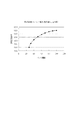
When the width of the partition area becomes smaller, an error of 1 μm occurs in both banks, and when ΔW becomes 2 μm, the variation rate of the layer thickness is as shown in FIG. 6, and the variation is within 3%. Is a case where the width of the partition area, that is, the pixel width is 70 μm or more.
ここでは、ストライプ状パターンに形成された区画領域を例にとって計算したので、L1はW1より十分に長いと仮定し、L1は一定とした。L1が短くなるほど、例えばバンク102を格子状パターンに形成した場合には、L1にもフォトリソによる変動分が大きく影響してくる。
Here, since the calculation is made by taking the partition area formed in the stripe pattern as an example, it is assumed that L1 is sufficiently longer than W1, and L1 is constant. As L1 becomes shorter, for example, when the
具体的に説明すると、図7のように、基板101上に形成したバンク802の片側にのみパターン誤差が発生した場合(805<803=804=806、ピッチ812〜814は等しい)、区画領域809の幅は他の区画領域よりも広くなる。バンクによる区画領域の幅の違いは区画領域の面積の違いとなり、有機EL塗布液を同じ量ずつ塗布すると、区画領域809に形成される有機化合物層301の層厚は薄くなってしまう。
More specifically, as shown in FIG. 7, when a pattern error occurs only on one side of the
(有機化合物層)
画素電極上に形成される有機化合物層には、ホール注入層、インターレイヤー、発光層等が含まれるが、インターレイヤーは材料の組み合わせによって省略することもできる。
(Organic compound layer)
The organic compound layer formed on the pixel electrode includes a hole injection layer, an interlayer, a light emitting layer, and the like, but the interlayer can be omitted depending on a combination of materials.
塗布法では、水や有機溶媒などの溶媒に有機化合物材料を溶かした有機EL塗布液を用いる。水溶性の有機化合物材料や有機溶媒に溶ける有機化合物材料を積層形成する場合、一旦形成した膜がその後塗布した有機化合物材料の溶媒に影響を受けないように、積層順に注意が必要である。特に、有機化合物層は水分によって非常に劣化しやすいため、一旦形成した有機化合物層の上に水溶性の有機化合物材料を塗布形成することはできない。 In the coating method, an organic EL coating solution in which an organic compound material is dissolved in a solvent such as water or an organic solvent is used. When stacking a water-soluble organic compound material or an organic compound material that is soluble in an organic solvent, care must be taken in order of stacking so that the film once formed is not affected by the solvent of the organic compound material applied thereafter. In particular, since the organic compound layer is very easily deteriorated by moisture, a water-soluble organic compound material cannot be formed by coating on the once formed organic compound layer.
一般的な塗布法による有機化合物層の積層方法は、まず水溶性のホール注入層材料を塗布し、水分を充分に揮発させてホール注入層を形成する。その後、有機溶媒に溶かしたインターレイヤーや発光層等の有機化合物材料を重ねて塗布し、溶媒を揮発させてインターレイヤーや発光層を形成する。このような順序で形成すれば、水溶性のホール注入層材料が有機溶媒に溶け出すことはなく、ホール注入層が水分で劣化することもない。 In a method of laminating an organic compound layer by a general coating method, first, a water-soluble hole injection layer material is applied, and water is sufficiently volatilized to form a hole injection layer. Thereafter, an organic compound material such as an interlayer or a light emitting layer dissolved in an organic solvent is applied in layers, and the solvent is volatilized to form the interlayer or the light emitting layer. If formed in this order, the water-soluble hole injection layer material does not dissolve in the organic solvent, and the hole injection layer does not deteriorate with moisture.
ここで、インターレイヤーとは、ホール注入層と発光層の間に設け、ホール注入層に含まれる物質、例えば酸性イオンが発光層に拡散して特性を劣化させるのを防止する層である。 Here, the interlayer is a layer which is provided between the hole injection layer and the light emitting layer and prevents substances contained in the hole injection layer, for example, acidic ions from diffusing into the light emitting layer and deteriorating the characteristics.
発光層の上にさらに電子注入層等の機能層を積層する場合は、蒸着法等の乾式法で形成することができる。 When a functional layer such as an electron injection layer is further laminated on the light emitting layer, it can be formed by a dry method such as an evaporation method.
(上部電極)
有機化合物層上には上部電極が形成される。上部電極には画素電極と同様の材料を用いることができる。ただし、発光した光を取り出すためには、画素電極と上部電極のいずれか一方を透明にしておかなければならない。光取り出し側に形成する電極には、透明導電膜や薄膜金属からなる半透過導電膜、あるいはそれらを積層した透光性の膜を用いる。
(Upper electrode)
An upper electrode is formed on the organic compound layer. A material similar to that for the pixel electrode can be used for the upper electrode. However, in order to extract the emitted light, either the pixel electrode or the upper electrode must be transparent. As the electrode formed on the light extraction side, a transparent conductive film, a semi-transmissive conductive film made of a thin film metal, or a translucent film in which these are laminated is used.
(封止構成)
上部電極までを形成した有機EL表示パネルは、水分や衝撃等の外部要因から保護するために封止される。ガラス等の透湿性の低い材料を、UV硬化性樹脂やガラスフリット等の接着剤で基板に接着した封止構成を用いることができる。また、SiNやSiO等の透湿性の低い無機膜や、樹脂膜と透湿性の低い無機膜との積層膜等で有機EL素子を覆う封止構成を用いることもできる。
(Sealing configuration)
The organic EL display panel formed up to the upper electrode is sealed to protect it from external factors such as moisture and impact. A sealing configuration in which a material having low moisture permeability such as glass is bonded to a substrate with an adhesive such as UV curable resin or glass frit can be used. Further, a sealing structure in which the organic EL element is covered with an inorganic film having low moisture permeability such as SiN or SiO, or a laminated film of a resin film and an inorganic film having low moisture permeability can be used.
トップエミッション構造の有機EL表示パネルの場合は、ガラスやSiN等の光透過率の高い材料を用い、ボトムエミッション構造の有機EL表示パネルの場合は、金属等の透過性の低い材料からなる封止管や膜を用いることができる
(製造方法)
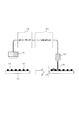
続いて、本発明の特徴である有機化合物層の形成工程について図1と図2を用いて詳しく説明する。有機化合物層の形成以外の工程には、従来の製造方法を用いることができる。
In the case of an organic EL display panel having a top emission structure, a material having a high light transmittance such as glass or SiN is used. In the case of an organic EL display panel having a bottom emission structure, sealing is made of a material having a low transmittance such as a metal. Tubes and membranes can be used (Manufacturing method)
Then, the formation process of the organic compound layer which is the characteristic of this invention is demonstrated in detail using FIG. 1 and FIG. Conventional processes can be used for processes other than the formation of the organic compound layer.
図1は有機EL材料を塗布して有機化合物層を形成する装置の模式図である。まず、画素電極103とバンク102とが形成された基板101は、その表面を画像取り込み装置104で撮影される。取得した画像データは画像処理装置105で画像処理され、バンク102による区画領域の位置と面積が算出される。位置データおよび面積データは吐出量制御装置106へ転送され、吐出量制御装置106はそれらのデータに応じて区画領域毎に吐出量を制御する。その結果、各区画領域には、それぞれの面積に応じた量の有機EL塗布液が塗布されるので、溶媒が揮発した後に各区画領域内に形成される有機化合物層の層厚は、ほぼ設計通りにすることができる。
FIG. 1 is a schematic view of an apparatus for forming an organic compound layer by applying an organic EL material. First, the surface of the
また、区画領域の面積変動は、バンクをパターニングする際の露光工程および現像工程の基板内のむらに起因する。同一の露光装置および現像装置を用いた同一工程においては、むらの発生する傾向が同じである。そこで、パターニングする際の露光工程および現像工程の基板面内のむらを事前に計測し、その結果に基づくアルゴリズムを吐出量制御装置に設定しておいても良い。そうすれば、同一装置かつ同一工程によって形成されるバンクに有機EL塗布液を塗布する際には、基板の一部の区画領域の面積を計測し、前記アルゴリズムによって基板面内の全体の区画領域を塗布することができる。これにより、タクトタイムを格段に短縮することができる。 The area variation of the partition region is caused by unevenness in the substrate in the exposure process and the development process when patterning the bank. In the same process using the same exposure apparatus and developing apparatus, the tendency for unevenness to occur is the same. Therefore, unevenness in the substrate surface of the exposure process and the development process at the time of patterning may be measured in advance, and an algorithm based on the result may be set in the discharge amount control device. Then, when applying the organic EL coating liquid to the bank formed by the same apparatus and the same process, the area of a part of the partition area of the substrate is measured, and the entire partition area in the substrate surface is measured by the algorithm. Can be applied. Thereby, the tact time can be remarkably shortened.
図2(a)は、1枚の大判基板内に表示パネルを複数形成する際に、各表示パネルの区画領域毎の吐出量を制御する方法として、吐出装置107の吐出口の走査速度を変える例を示した図である。図2(b)は(a)の表示パネル1つを拡大した図である。表示パネルにはストライプ状パターンのバンクが形成されている。バンクは有機EL塗布液の塗布方向と並行な方向だけでなく、その開始端と終端にも設けられ、有機EL塗布液を塗布する領域はバンク102で区画されている。各表示パネルの区画領域ごとに吐出量を制御するには、位置データおよび面積データに応じて、吐出装置107に設けられた吐出口の走査速度υを制御することが簡便で、現実的である。ここで、吐出口の走査速度υは、基板と吐出口の相対速度の意味であって、吐出口を動かしても良いし、基板を動かしても良いし、その両方を動かしても良い。
FIG. 2A shows a method of changing the ejection speed of the ejection port of the
吐出口の走査速度υによって区画領域内の吐出量を制御する方法は、ディスペンス法に最適であるが、インクジェット法にも用いることができる。インクジェット法を用いる場合は、各表示パネル毎の区画領域の位置データおよび面積データに応じて、各区画領域内の吐出回数を変えても良い。 The method of controlling the discharge amount in the partition area by the scanning speed υ of the discharge port is optimal for the dispensing method, but can also be used for the ink jet method. When the inkjet method is used, the number of ejections in each partition area may be changed according to the position data and area data of the partition area for each display panel.
また、吐出量制御装置106は、吐出量の制御の他に塗布液の濃度を制御するものであってもよい。この場合、吐出量制御装置106は、装置内に基準濃度の有機EL塗布液と溶媒とを備え、区画領域の面積に応じて高速で塗布液中の有機化合物材料の濃度を制御することができる。基準濃度の塗布液に流量制御された溶媒が混合され、濃度が調整される。濃度調整された有機EL塗布液は、吐出口から各区画領域に塗布される。その結果、有機EL塗布液の吐出量を調整した場合と同様に、区画領域の面積に応じて、ほぼ設計値通りの層厚の有機化合物層を形成することができる。
Further, the discharge
画像取り込み装置104は、塗布動作以前に画像処理と吐出装置の制御データが形成できれば、図1のように吐出装置107とは別の装置であっても良いし、吐出装置107と一体化されていても良い。
The
(実施例1)
図1は、本発明にかかる製造装置の有機化合物層形成装置の模式図である。
Example 1
FIG. 1 is a schematic view of an organic compound layer forming apparatus of a manufacturing apparatus according to the present invention.
ITOからなる画素電極103などを作製した基板101上の画素間に、ポリイミド樹脂でバンク102を形成した。バンク102にはフッ素ラジカルを用いて撥水処理が行われている。バンクの幅は設計値5μmを中心値として、±1μmの範囲内でばらついていた。バンクは画素の長さ方向に区画するストライプ状とし、区画領域すなわち画素の幅は27μmとした。
A
300mm×350mmサイズの基板101に、2.5インチ(対角2.5インチ)の大きさの表示パネルを縦に4個、横に3個、合計12個(パネル201〜212)を形成した。図2(a)に表示パネルが形成された基板101の平面図を示す。
A total of 12 display panels (
まず、基板面内に形成した区画領域の形状を画像取り込み装置104で撮影し、取得した画像データを画像処理装置105で処理して各区画領域の面積を算出し、面積データを吐出量制御装置106へ転送した。吐出量制御装置は、面積データに応じて画領域毎に吐出口の走査速度を制御し、吐出装置107から吐出する塗布液の量を適宜変化させた。1つの区画領域内の塗布速度をυとすると、図8のようにυをパネル毎に変化した。
First, the shape of the partition area formed in the substrate surface is photographed by the
塗布方式は、塗布液をパルス的に吐出するインクジェット法を採用した。 As the coating method, an inkjet method in which the coating liquid is ejected in a pulse manner is employed.
特開2007−200836有機EL塗布液には、純水に溶かしたホール注入材料のPEDOT/PSS液を用いた。 As the organic EL coating solution, a PEDOT / PSS solution of hole injection material dissolved in pure water was used.
パネル201〜212のすべてのパネルにおける溶媒揮発後のPEDOT/PSS層の層厚は、設計層厚50nmに対して50nm±0.9nmと、ずれは3%以内であった。
The thickness of the PEDOT / PSS layer after solvent evaporation in all the
(比較例1)
実施例1と同様の基板に、画像取り込み装置104や、画像処理装置105を取り外し、吐出量を一定に保つ吐出装置を用いて、実施例1と同じPEDOT/PSS液を塗布形成した。乾燥後に得られたPEDOT/PSS層の膜厚を測定したところ、パネル201〜212の全体で、設計層厚に50nmに対して50nm±3.5nmとなり、層厚の目標スペックとしている±3%以下を達成しなかった。
(Comparative Example 1)
The same PEDOT / PSS solution as in Example 1 was applied and formed on the same substrate as in Example 1 using an ejection device that removed the
(実施例2)
本実施例では、吐出量の制御に変えて、塗布液の濃度を制御して有機化合物層を塗布した。
(Example 2)
In this example, the organic compound layer was applied by controlling the concentration of the coating liquid instead of controlling the discharge amount.
フッ素樹脂が含有された感光性エポキシ樹脂でバンク102を形成したこと以外は、実施例1と同様にしてバンクまでを形成した。バンクはそのままで撥液能力が備わっている。
A bank up to the bank was formed in the same manner as in Example 1 except that the
バンクによる区画領域の形状を画像取り込み装置104で撮影し、取得したデータを画像処理装置105で処理して各区画領域の面積を算出し、吐出量制御装置106へ転送した。吐出量制御装置106は面積データに応じて区画領域毎吐出装置107から吐出する塗布液の濃度を適宜変化させた。塗布液濃度をc、溝内液量をV、膜厚dの関係は、図13に示した通りである。このとき、速度υは一定とした。
The shape of the partition area by the bank was photographed by the
塗布方式は、塗布液を連続的に吐出するディスペンス法を採用した。 As a coating method, a dispensing method in which a coating solution is continuously discharged is adopted.
有機EL塗布液として、発光層材料のポリパラフェニレンビニレン誘導体poly[2−methoxy,5−(2´−ethylhexoxy)−1,4−phenylen vinylene]をアニソールで希釈したものを塗布した。 As an organic EL coating solution, a solution obtained by diluting a polyparaphenylene vinylene derivative poly [2-methyl, 5- (2′-ethylhexoxy) -1,4-phenylene vinylene] with anisole as a light emitting layer material was applied.
パネル201〜212のすべてのパネルにおける乾燥後の発光層の層厚は、設計値80nmに対して、80nm±1.8nmとずれは3%以内であった。
The thickness of the light emitting layer after drying in all the
(実施例3)
本実施例では、パネル2個分が入るサイズのフォトマスクを用い、365mm×460mmサイズの基板上に、縦に6個、横に6個の計36個のパネルに該当するバンクをフォトリソにて形成した。図14に本実施例にかかるパネルの一部分を示した。
(Example 3)
In this embodiment, a photomask of a size that can accommodate two panels is used, and a bank corresponding to a total of 36 panels, 6 vertically and 6 horizontally, is formed by photolithography on a 365 mm × 460 mm size substrate. Formed. FIG. 14 shows a part of the panel according to this example.
基板上にバンクを形成する際の露光装置のフォトマスク903のサイズは、図14に示すようにパネル2個分とした。このフォトマスク903を用いて、同一の露光装置でパネル2個分の露光を繰り返し、基板面内の全体にフォトリソ工程を施した。
The size of the
バンクの材料には実施例2と同じ材料を用いたところ、バンクの幅は設計値5μmを中心値として、±1μmの範囲でばらついていた。バンクによって区画される領域の幅は27μmとした。 When the same material as in Example 2 was used as the bank material, the bank width varied within a range of ± 1 μm with a design value of 5 μm as the center value. The width of the area partitioned by the bank was 27 μm.
まず、基板面内の一部分、つまり1回の露光でパターニングされる2個のパネル(901と902)の区画領域の形状を、画像取り込み装置104で撮影した。そして、基板上の他のパネルの区画領域の形状は、前記露光パターンの繰り返し、つまり、前記画像データの繰り返しであると仮定して、画像処理装置105で基板全体の画像データに処理し、吐出量制御装置106へ転送した。吐出量制御装置は、該画像データに応じてバンクによる区画領域ごとに有機EL塗布液の濃度を制御し、吐出装置107から吐出する有機化合物材料の量を適宜変化させた。塗布液の濃度をc1、溝内液量をV1、膜厚d1の関係は、図13に示した通りである。このとき、速度υは一定とした。
First, a part of the substrate surface, that is, the shape of the partition area of two panels (901 and 902) patterned by one exposure was photographed by the
塗布方式は、塗布液を連続的に吐出するディスペンス方式を採用した。 As the coating method, a dispensing method that continuously discharges the coating solution was adopted.
有機EL塗布液は、発光層材料のポリパラフェニレンビニレン誘導体poly[2−methoxy,5−(2´−ethylhexoxy)−1,4−phenylen vinylene]をアニソールで希釈したものを用いた。 As the organic EL coating solution, a solution obtained by diluting a polyparaphenylene vinylene derivative poly [2-methoxy, 5- (2′-ethylhexoxy) -1,4-phenylene vinylene], which is a light emitting layer material, with anisole was used.
基板面内のすべての表示パネルにおける乾燥後の発光層の膜厚は、80nm±2.0nmであった。 The thickness of the light emitting layer after drying in all the display panels in the substrate surface was 80 nm ± 2.0 nm.
以上より、大型の基板に対して、フォトマスク1枚を複数回繰り返して使用する場合、できあがった区画領域の形状は、フォトマスク1回使用時の繰り返しとなる。すなわち、大型の基板上の区画領域の形状は、その部分的な計測をもって全体が容易に予想され、区画領域毎に濃度を変化させるによって膜厚を制御することができた。 As described above, when one photomask is repeatedly used for a large-sized substrate, the shape of the partition area is the same as the one-time use of the photomask. In other words, the shape of the partitioned area on the large substrate was easily predicted as a whole by partial measurement, and the film thickness could be controlled by changing the concentration for each partitioned area.
本実施例では有機EL塗布液の濃度を制御したが、本実施例と同様に、基板の区画領域の部分的な計測をもって全体を予想し、吐出口の速度を制御しても膜厚を制御することができる。 In this example, the concentration of the organic EL coating solution was controlled, but as in this example, the whole was predicted by partial measurement of the partition area of the substrate, and the film thickness was controlled even if the ejection port speed was controlled. can do.
(実施例4)
図4は本発明による有機EL表示パネルの模式図である。300mm×350mmのガラス基板101上に、長さ90μmのITO電極103、感光性エポキシ樹脂でバンク102を形成した。バンク102は、実施例2と同様に後処理無しで撥液性がある。バンクの幅は設計値5μmを中心値として、±1μmの範囲内でばらついていた。区画領域の幅は27μmとした。本実施例の基板も、実施例1と同様、1枚の大判基板で、パネル数12個が一度に作製出来る。
Example 4
FIG. 4 is a schematic view of an organic EL display panel according to the present invention. A
ディスペンス法を用いた他は実施例1と同様にして、区画領域の面積に応じて吐出口の走査速度変化させてPEDOT/PSS層を塗布し、その後溶媒を充分揮発させてホール注入層50nmを形成した。続いて、発光層材料には、ポリパラフェニレンビニレン誘導体poly[2−methoxy,5−(2´−ethylhexoxy)−1,4−phenylen vinylene]を用いた。実施例2と同様にアニソールで希釈してホール注入層の上に塗布し、溶媒を充分乾燥させて80nmの発光層を形成した。 Except for using the dispensing method, the PEDOT / PSS layer was applied by changing the scanning speed of the discharge port according to the area of the partition region in the same manner as in Example 1, and then the solvent was sufficiently volatilized to form a hole injection layer of 50 nm. Formed. Subsequently, a polyparaphenylene vinylene derivative poly [2-methyoxy, 5- (2′-ethylhexoxy) -1,4-phenylene vinylene] was used as the light emitting layer material. In the same manner as in Example 2, it was diluted with anisole and applied onto the hole injection layer, and the solvent was sufficiently dried to form an 80 nm light emitting layer.
その後、電子注入層としてCsCoを35nmと、上部電極としてAl層401を100nmを真空蒸着で形成し、表示パネルごとに封止部材402としてガラスキャップをUV硬化性樹脂で接着し、封止した。
Thereafter, 35 nm of CsCo as an electron injection layer and 100 nm of an
最後に大判基板をスクライバーで切断し、12個の表示パネルに分割した。
作製した表示パネルの取り出し電極に電源と外部回路を接続して発光させたところ、輝度は約300cd/cm2で、官能試験で人間の目には輝度バラツキを見つけることはできなかった。表示パネルにおけるホール注入層および発光層の設計値からの層厚誤差を検査するため、表示パネル内の複数箇所の断面SEM観察したところ、ホール注入層および発光層のどちらも設計層厚からの誤差は3%以内であった。
Finally, the large substrate was cut with a scriber and divided into 12 display panels.
When a power source and an external circuit were connected to the extraction electrode of the manufactured display panel to emit light, the luminance was about 300 cd / cm 2, and no luminance variation could be found in the human eye through a sensory test. In order to inspect the layer thickness error from the design values of the hole injection layer and the light emitting layer in the display panel, cross-sectional SEM observations at a plurality of locations in the display panel showed that both the hole injection layer and the light emitting layer had errors from the design layer thickness. Was within 3%.
このような有機発光パネルは、図12に示すようなデジタルカメラ1401、携帯端末1402、テレビ1403などに応用することが可能である。
Such an organic light-emitting panel can be applied to a
101 基板
102、802、815 バンク(隔壁)
103、816 画素電極
104 画像取り込み装置
105 画像処理装置
106 吐出量制御装置
107 吐出装置
108 塗布装置から吐出した溶液
109 有機EL塗布液の乾燥前の液面高さ
201〜212、901、902 パネル
301 有機化合物層
401 上部電極(カソード電極)
402 封止部材
501 反射電極
803、804、805、806 バンク幅
807、808、809、810 区画領域幅
811、812、813、814 画素ピッチ
903 バンクパターニング用のフォトマスク
1401 デジタルカメラ
1402 携帯端末
1403 テレビ
101
103, 816
402
Claims (4)
前記区画された領域それぞれの面積を取得する工程と、
前記取得された面積に応じて前記塗布液の量あるいは濃度を制御しながら、前記区画された領域内に前記塗布液を吐出する工程と、
を有することを特徴とする有機EL表示パネルの製造方法。 An organic EL element including an organic compound layer disposed between electrodes in a substrate surface, wherein the organic compound layer is formed by applying a coating solution in which an organic compound material is dissolved in a solvent in a partitioned area. A method for manufacturing an organic EL display panel in which a plurality of organic EL display panels are formed from a single substrate,
Obtaining an area of each of the partitioned regions;
Discharging the coating liquid into the partitioned area while controlling the amount or concentration of the coating liquid according to the acquired area;
A method for producing an organic EL display panel, comprising:
前記取得された面積に応じて前記塗布液の量を制御しながら、前記区画された領域内に前記塗布液を吐出する工程は、前記基板面内の一部の区画された領域の面積と予め設定されたアルゴリズムとに従って塗布液の量を制御する工程であることを特徴とする請求項1に記載の有機EL表示パネルの製造方法。 The step of acquiring the area of each of the partitioned regions is a step of acquiring the area of the partitioned region provided in a part of the substrate surface,
The step of discharging the coating liquid into the partitioned area while controlling the amount of the coating liquid according to the acquired area is performed in advance with the area of a part of the partitioned area in the substrate surface. 2. The method of manufacturing an organic EL display panel according to claim 1, wherein the amount of the coating liquid is controlled in accordance with a set algorithm.
前記基板面内の一部の区画された領域の画像を取得する手段と、
前記取得した画像から前記一部の区画された領域それぞれの面積を算出する手段と、
前記算出した基板面内の一部について算出した面積と予め設定されたアルゴリズムとから、前記基板面内の全体の区画された領域それぞれに塗布する塗布液の量あるいは濃度を算出する手段と、
前記算出した量あるいは濃度の塗布液を吐出する吐出量制御手段と、
前記塗布液を吐出する吐出口と、
を有することを特徴とする塗布装置。 A coating apparatus for coating a coating liquid in a partitioned area in a substrate surface,
Means for obtaining an image of a part of the partitioned area in the substrate surface;
Means for calculating the area of each of the partial partitioned regions from the acquired image;
Means for calculating the amount or concentration of the coating liquid to be applied to each of the entire partitioned area in the substrate surface from the area calculated for a part in the calculated substrate surface and a preset algorithm;
A discharge amount control means for discharging the calculated amount or concentration of the coating liquid;
A discharge port for discharging the coating liquid;
A coating apparatus comprising:
Priority Applications (1)
| Application Number | Priority Date | Filing Date | Title |
|---|---|---|---|
| JP2008272131A JP2010102892A (en) | 2008-10-22 | 2008-10-22 | Method and device for producing organic el display panel |
Applications Claiming Priority (1)
| Application Number | Priority Date | Filing Date | Title |
|---|---|---|---|
| JP2008272131A JP2010102892A (en) | 2008-10-22 | 2008-10-22 | Method and device for producing organic el display panel |
Publications (1)
| Publication Number | Publication Date |
|---|---|
| JP2010102892A true JP2010102892A (en) | 2010-05-06 |
Family
ID=42293378
Family Applications (1)
| Application Number | Title | Priority Date | Filing Date |
|---|---|---|---|
| JP2008272131A Pending JP2010102892A (en) | 2008-10-22 | 2008-10-22 | Method and device for producing organic el display panel |
Country Status (1)
| Country | Link |
|---|---|
| JP (1) | JP2010102892A (en) |
Cited By (3)
| Publication number | Priority date | Publication date | Assignee | Title |
|---|---|---|---|---|
| JP2013188737A (en) * | 2012-02-16 | 2013-09-26 | Tdk Corp | Liquid material discharge device |
| WO2022180481A1 (en) * | 2021-02-26 | 2022-09-01 | 株式会社半導体エネルギー研究所 | Display apparatus and electronic equipment |
| WO2025005210A1 (en) * | 2023-06-30 | 2025-01-02 | 武蔵エンジニアリング株式会社 | Liquid coating method and liquid coating device |
-
2008
- 2008-10-22 JP JP2008272131A patent/JP2010102892A/en active Pending
Cited By (9)
| Publication number | Priority date | Publication date | Assignee | Title |
|---|---|---|---|---|
| JP2013188737A (en) * | 2012-02-16 | 2013-09-26 | Tdk Corp | Liquid material discharge device |
| WO2022180481A1 (en) * | 2021-02-26 | 2022-09-01 | 株式会社半導体エネルギー研究所 | Display apparatus and electronic equipment |
| JPWO2022180481A1 (en) * | 2021-02-26 | 2022-09-01 | ||
| US12455446B2 (en) | 2021-02-26 | 2025-10-28 | Semiconductor Energy Laboratory Co., Ltd. | Display device with light emitting device and light sensing device in one layer |
| WO2025005210A1 (en) * | 2023-06-30 | 2025-01-02 | 武蔵エンジニアリング株式会社 | Liquid coating method and liquid coating device |
| JPWO2025005210A1 (en) * | 2023-06-30 | 2025-01-02 | ||
| KR20250051796A (en) * | 2023-06-30 | 2025-04-17 | 무사시 엔지니어링 가부시키가이샤 | Liquid application method and liquid application device |
| JP7708486B2 (en) | 2023-06-30 | 2025-07-15 | 武蔵エンジニアリング株式会社 | Liquid application method and liquid application device |
| KR102862219B1 (en) | 2023-06-30 | 2025-09-18 | 무사시 엔지니어링 가부시키가이샤 | Liquid application method and liquid application device |
Similar Documents
| Publication | Publication Date | Title |
|---|---|---|
| US12167663B2 (en) | High resolution organic light-emitting diode devices, displays, and related methods | |
| JP3915810B2 (en) | ORGANIC ELECTROLUMINESCENCE DEVICE, ITS MANUFACTURING METHOD, AND ELECTRONIC DEVICE | |
| US7897211B2 (en) | Method for forming film pattern and method for manufacturing an organic EL device, a color filter substrate and a liquid crystal display device | |
| JP4211804B2 (en) | Device, film forming method and device manufacturing method | |
| JP5061562B2 (en) | LIGHT EMITTING DEVICE AND ELECTRONIC DEVICE | |
| JP4998710B2 (en) | Manufacturing method of display device | |
| CN1992157B (en) | Display device manufacturing device and display device manufacturing method | |
| CN111192979B (en) | Method for manufacturing display panel and functional layer forming apparatus | |
| JP2009081097A (en) | Electro-optical device and electronic apparatus | |
| JP2007311235A (en) | Device, film forming method, and device manufacturing method | |
| JP2005276479A (en) | ELECTRO-OPTICAL DEVICE, MANUFACTURING METHOD THEREOF, AND ELECTRONIC DEVICE | |
| JP2007311236A (en) | Device, film forming method and device manufacturing method | |
| JP4497156B2 (en) | Organic electroluminescence device and electronic device | |
| JP2007080603A (en) | Film pattern forming method, device manufacturing method, organic electroluminescence apparatus | |
| JP2010102892A (en) | Method and device for producing organic el display panel | |
| JP4306599B2 (en) | Pattern forming substrate, electro-optical device, and method of manufacturing electro-optical device | |
| JP2004198486A (en) | Image display device and method of manufacturing the same | |
| JP2007280866A (en) | Thin film device, organic EL device and liquid crystal display device, electronic device, method for manufacturing thin film device, method for manufacturing organic EL device, and method for manufacturing liquid crystal display device | |
| JP2007044582A (en) | Surface treatment method, electro-optical device manufacturing method, and electro-optical device | |
| JP4631609B2 (en) | Functional film forming method, organic EL display panel manufacturing method, liquid crystal display panel manufacturing method, plasma display panel manufacturing method, color filter manufacturing method | |
| JP2014191979A (en) | Light-emitting device and manufacturing method thereof | |
| JP2005183184A (en) | Manufacturing method of organic EL display device | |
| JP5082217B2 (en) | Film pattern forming method, device manufacturing method | |
| JP2010092595A (en) | Method and device for manufacturing organic el element | |
| JP2011054512A (en) | Method for manufacturing optical device |
Legal Events
| Date | Code | Title | Description |
|---|---|---|---|
| RD04 | Notification of resignation of power of attorney |
Free format text: JAPANESE INTERMEDIATE CODE: A7424 Effective date: 20100201 |
|
| RD01 | Notification of change of attorney |
Free format text: JAPANESE INTERMEDIATE CODE: A7421 Effective date: 20100630 |