JP2010040693A - Method for forming pattern - Google Patents
Method for forming pattern Download PDFInfo
- Publication number
- JP2010040693A JP2010040693A JP2008200550A JP2008200550A JP2010040693A JP 2010040693 A JP2010040693 A JP 2010040693A JP 2008200550 A JP2008200550 A JP 2008200550A JP 2008200550 A JP2008200550 A JP 2008200550A JP 2010040693 A JP2010040693 A JP 2010040693A
- Authority
- JP
- Japan
- Prior art keywords
- pattern
- electrodeposition
- metal pattern
- seed layer
- metal
- Prior art date
- Legal status (The legal status is an assumption and is not a legal conclusion. Google has not performed a legal analysis and makes no representation as to the accuracy of the status listed.)
- Pending
Links
Images


Landscapes
- Other Surface Treatments For Metallic Materials (AREA)
- Electrodes Of Semiconductors (AREA)
- Internal Circuitry In Semiconductor Integrated Circuit Devices (AREA)
- Electroplating Methods And Accessories (AREA)
Abstract
Description
本発明は、電着による膜が形成されるパターンの形成方法に関するものである。 The present invention relates to a method for forming a pattern in which a film is formed by electrodeposition.
LSIやMEMS(Micro Electro Mechanical Systems)において、パターンの保護などのためにパターンの表面に電着により膜を形成する技術が用いられている。例えば、可動部と固定電極との接触による固着を防ぐために、電着により膜を形成している(特許文献1参照)。電着による膜の形成では、電圧を印加している部分に選択的に膜を形成することができるため、所望とする領域に膜を形成できるという利点を有している。 In LSI and MEMS (Micro Electro Mechanical Systems), a technique for forming a film by electrodeposition on the surface of a pattern is used to protect the pattern. For example, in order to prevent sticking due to contact between the movable part and the fixed electrode, a film is formed by electrodeposition (see Patent Document 1). Formation of a film by electrodeposition has an advantage that a film can be formed in a desired region because a film can be selectively formed in a portion to which a voltage is applied.
しかしながら、上述したような電着による膜の形成では、電着をするパターンに電圧を印加するための配線構造が必要となる。しかしながら、この配線構造は、電着のために用いるものであり、作製されるLSIやMEMSなどの微細装置においては不要なものとなり、微細装置の上においては無駄な部分となる。これに対し、例えば、特許文献1では、複数の微細装置を同時に形成する基板の断裁領域に、電着のための配線構造を設け、この配線構造による無駄を抑制している。しかしながら、微細装置上の電着用の配線は依然として残存することになり、また、電着のための配線構造を別途に設けることには何ら変わりはない。このように、従来では、LSIやMEMSなどの技術において、所望とするパターンに電着膜を形成する場合、装置上では無駄となる電着のための配線を形成することになるという問題があった。 However, the formation of a film by electrodeposition as described above requires a wiring structure for applying a voltage to the pattern to be electrodeposited. However, this wiring structure is used for electrodeposition, and is unnecessary in a fine device such as LSI or MEMS to be manufactured, and is a useless part on the fine device. On the other hand, for example, in Patent Document 1, a wiring structure for electrodeposition is provided in a cutting region of a substrate on which a plurality of fine devices are formed simultaneously, and waste due to this wiring structure is suppressed. However, the electrodeposition wiring on the fine device still remains, and there is no change in separately providing a wiring structure for electrodeposition. As described above, conventionally, when an electrodeposition film is formed in a desired pattern in technologies such as LSI and MEMS, there is a problem that wiring for electrodeposition that is wasted on the apparatus is formed. It was.
本発明は、以上のような問題点を解消するためになされたものであり、無駄を省いた状態で、所望とする微細なパターンに電着による膜が形成できるようにすることを目的とする。 The present invention has been made to solve the above-described problems, and it is an object of the present invention to form a film by electrodeposition on a desired fine pattern while eliminating waste. .
本発明に係るパターン形成方法は、基板の上に金属より構成されたシード層を形成する工程と、シード層の上に開口パターンを備えたレジスト膜を形成する工程と、開口パターンに露出するシード層の上にめっきにより金属パターンを形成する工程と、シード層に電圧を印加する電着により、金属パターンの一部が露出する開口部において露出している金属パターンの表面に電着膜を形成する工程と、レジスト膜を除去する工程と、金属パターンをマスクとしてシード層を選択的にエッチングして分離する工程とを少なくとも備える。 The pattern forming method according to the present invention includes a step of forming a seed layer made of metal on a substrate, a step of forming a resist film having an opening pattern on the seed layer, and a seed exposed to the opening pattern. Forming a metal pattern by plating on the layer and electrodeposition by applying a voltage to the seed layer to form an electrodeposition film on the surface of the metal pattern exposed at the opening where part of the metal pattern is exposed And a step of removing the resist film, and a step of selectively etching and separating the seed layer using the metal pattern as a mask.
上記パターン形成方法において、電着膜を形成するときの開口部は、レジスト膜の開口パターンであればよい。また、電着膜を形成するときの開口部は、レジスト膜を除去して新たに形成したレジスト膜に形成した新たな開口パターンであってもよい。 In the pattern formation method, the opening when forming the electrodeposition film may be an opening pattern of a resist film. Further, the opening when the electrodeposition film is formed may be a new opening pattern formed in the newly formed resist film by removing the resist film.
上記パターン形成方法において、金属パターンを形成した後、開口部の側面と金属パターンとの間に隙間を形成して金属パターンの上面および側面を露出させ、金属パターンの露出している上面および側面に電着膜を形成するようにしてもよい。この場合、金属パターンを形成した後、金属パターンをエッチングすることで、開口部を側面と金属パターンとの間に隙間を形成して金属パターンの上面および側面を露出させればよい。また、金属パターンを形成した後、開口部を広げることで、開口部を側面と金属パターンとの間に隙間を形成して金属パターンの上面および側面を露出させるようにしてもよい。 In the pattern forming method, after the metal pattern is formed, a gap is formed between the side surface of the opening and the metal pattern to expose the upper surface and the side surface of the metal pattern, and on the exposed upper surface and the side surface of the metal pattern. An electrodeposition film may be formed. In this case, after the metal pattern is formed, the metal pattern is etched to form a gap between the side surface and the metal pattern to expose the upper surface and the side surface of the metal pattern. Further, after forming the metal pattern, the opening may be widened to form a gap between the side surface and the metal pattern so that the upper surface and the side surface of the metal pattern are exposed.
上記パターン形成方法において、シード層を選択的にエッチングして分離した後、金属パターンの電着膜で被覆されていない側面をエッチングする工程を新たに備えるようにしてもよい。また、シード層および金属パターンの一部は、基板の上に形成した犠牲パターン上に形成し、金属パターンをマスクとしてシード層を選択的にエッチングして分離した後、犠牲パターンを除去し、シード層および金属パターンの一部で、基板の上に可動構造体を形成するようにしてもよい。 In the pattern forming method, after the seed layer is selectively etched and separated, a step of etching the side surface not covered with the electrodeposition film of the metal pattern may be newly provided. The seed layer and a part of the metal pattern are formed on the sacrificial pattern formed on the substrate, and the seed layer is selectively etched and separated using the metal pattern as a mask, and then the sacrificial pattern is removed and the seed is removed. The movable structure may be formed on the substrate with a part of the layer and the metal pattern.
上記パターン形成方法において、電着膜で覆われた金属パターンを覆う絶縁膜を形成する工程を新たに備えるようにしてもよい。また、電着に用いる電着液は、スルフォニウムイオンを電着成分として含んでいるもであればよい。 In the pattern forming method, a step of forming an insulating film covering the metal pattern covered with the electrodeposition film may be newly provided. Moreover, the electrodeposition liquid used for electrodeposition should just contain the sulfonium ion as an electrodeposition component.
以上説明したように、本発明によれば、シード層に電圧を印加する電着により、シード層にめっきされた金属パターンの一部が露出する開口部において露出している金属パターンの表面に電着膜を形成するようにしたので、無駄を省いた状態で、所望とする微細なパターンに電着による膜が形成できるようになるという優れた効果が得られる。 As described above, according to the present invention, the electrodeposition on the surface of the metal pattern exposed at the opening where a part of the metal pattern plated on the seed layer is exposed by electrodeposition of applying a voltage to the seed layer. Since the deposited film is formed, it is possible to obtain an excellent effect that a film can be formed by electrodeposition in a desired fine pattern without waste.
以下、本発明の実施の形態について図を参照して説明する。 Hereinafter, embodiments of the present invention will be described with reference to the drawings.
[実施の形態1]
はじめに、本発明の実施の形態1について図1A〜図1Iを用いて説明する。図1A〜図1Iは、本発明の実施の形態1におけるパターン形成方法を説明するための工程図であり、図1A,図1C〜図1Iは、模式的な断面図であり、図1Bは平面図である。
[Embodiment 1]
First, Embodiment 1 of the present invention will be described with reference to FIGS. 1A to 1I. 1A to 1I are process diagrams for explaining a pattern forming method according to Embodiment 1 of the present invention. FIGS. 1A and 1C to 1I are schematic cross-sectional views, and FIG. 1B is a plan view. FIG.
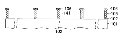
まず、図1Aに示すように、例えば単結晶シリコンなどの半導体材料からなる基板101の上に、シード層102を形成する。シード層102は、例えばTiからなる膜厚0.1μm程度の下層と、例えばAuからなる膜厚0.1μm程度の上層とを備えている。これらは、よく知られた蒸着法により形成することができる。このようにAuからなるシード層102を用いることで、後述するように、めっき法によりAuからなる金属パターンが形成可能である。また、チタンからなる下層は、金からなる上層と基板101との密着性を向上させるために備える。なお、基板101の表面に、例えば、酸化シリコン層(図示せず)を形成し、この上にシード層102を形成すればよい。
First, as shown in FIG. 1A, a
次に、シード層102の上に、公知のフォトリソグラフィ技術により、例えば、よく知られたポジ型のフォトレジスト材料からなる膜厚12μmのレジスト膜103を形成する。レジスト膜103は、所望の箇所に、シード層102に達する開口パターン103aを備える。また、図1Bの平面図に示すように、基板101の周端部101aの領域においては、レジスト膜103が無く、基板101が露出した状態とする。この基板101の端部の露出部は、基板101の全周に渡って形成する必要はなく、一部に露出する箇所が設けられていればよい。なお、図1Bにおいて、一点鎖線は、チップ領域を仮想的に示しているものである。
Next, a 12 μm-
次に、図1Cに示すように、シード層102の露出している箇所に、Auより構成された金属パターン104,金属パターン105を形成する。これらの金属パターンは、シード層102を一方の電極とする電解めっき法により、膜厚10μm程度にAuを堆積することで形成すればよい。例えば、Auめっき液に基板101を浸漬し、この中で、対向電極とシード層102との間に必要な電圧を印加することで、例えば、開口パターン103aに露出しているシード層102の上にAuを堆積することができる。このとき、基板101の外周部で露出しているシード層102に必要な配線を接続することで、シード層102に必要な電圧を印加すればよい。
Next, as shown in FIG. 1C, a
次に、シード層102に負電圧を印加する電着により、図1Dに示すように、開口部である開口パターン103aにおいて露出している金属パターン104および金属パターン105の上面に、例えば膜厚1μm程度の電着絶縁膜106を形成する。電着絶縁膜106の形成では、まず、容器151内に電着液152を収容し、電着液152の中で、白金からなる対向電極153に基板101の金属パターン104形成面を対向させて配置する。電着液152には、例えば、エポキシ基を有するスルフォニウムイオン(カチオン)を電着成分として含むもの(日本ペイント株式会社;インシュリードINSULEED3020)を用いることができる。例えば、液温30℃として用いればよい。
Next, by electrodeposition applying a negative voltage to the
この状態で、定電圧源154により、対向電極153に正電圧を印加し、シード層102に負電圧を印加する。ここで、金属パターン105に必要な配線を接続することで、シード層102に対する負電圧の印加を行う。このようなカチオン電着により、金属パターン104および金属パターン105の露出している面(上面)に、電着液152中の電着成分が付着(析出)し、電着絶縁膜106が形成される。
In this state, the
以上のようにして電着絶縁膜106を形成した後、電着液152の中より基板101を引き上げ、基板101を水洗処理して乾燥させた後、窒素雰囲気において110℃25分の加熱処理を行い、電着絶縁膜106を熱硬化する(図1E)。加熱処理により、電着絶縁膜106は硬化し、また、電着絶縁膜106と金属パターン104(金属パターン105)との密着性が向上する。
After the
次に、レジスト膜103を除去することで、図1Fに示すように、シード層102の上に、金属パターン104,金属パターン105が形成され、金属パターン104,金属パターン105の上に電着絶縁膜106が選択的に形成された状態が得られる。例えば、Nメチルピロリドンなどの剥離液を用いることで、レジスト膜103を除去すればよい。
Next, by removing the resist
次に、金属パターン104,金属パターン105をマスクとしてシード層102をエッチング除去することで、図1Gに示すように、基板101の上で、金属パターン104,金属パターン105毎に、シード層102を分離(絶縁分離)する。シード層102の上層の金層のエッチングには希王水を用い、下層のチタン層のエッチングにはフッ酸溶液を用いればよい。
Next, by removing the
ここで、上述した希王水を用いたシード層102の上層(金層)のエッチングにおいて、処理時間をより長くし、またより高い濃度の王水を用いることなどにより、電着絶縁膜106をマスクとし、金属パターン104(シード層102を含む)の側部をエッチングし、図1Hに示すように、平面方向の寸法がより小さい金属パターン141を形成することもできる。また、この後、図1Iに示すように、例えば酸素プラズマの処理(ドライエッチング)により電着絶縁膜106を除去すれば、基板101の上に金属パターン141が形成された状態が得られる。
Here, in the etching of the upper layer (gold layer) of the
以上に説明したように、本実施の形態によれば、電着のための専用の配線構造を形成することなく、無駄を省いた状態で、所望とする金属パターン(微細なパターン)に電着による膜を形成することができる。また、このように電着による膜(パターン)を形成することができるので、めっきなどにより厚膜に形成する金属パターンのアスペクト比をより高くすることができる。 As described above, according to the present embodiment, electrodeposition is performed on a desired metal pattern (fine pattern) without forming a dedicated wiring structure for electrodeposition and without waste. A film can be formed. Further, since a film (pattern) by electrodeposition can be formed in this way, the aspect ratio of the metal pattern formed on the thick film by plating or the like can be further increased.
例えば、膜厚10μm程度の金属パターンを形成する場合、上述したように、形成した金属パターンの箇所に開口部を有するフォトレジストのパターンを形成している。しかしながら、このような厚膜の金属パターンを形成する場合、フォトレジストも厚膜にすることになる。ところが、フォトリソグラフィの限界のために、厚膜化にともない開口可能な最小寸法が大きくなる。このため、形成する金属パターンの幅を小さくすることが困難となり、高アスペクト比の金属パターンを形成することが容易ではない状態となる。 For example, when forming a metal pattern with a film thickness of about 10 μm, as described above, a photoresist pattern having an opening at the location of the formed metal pattern is formed. However, when such a thick metal pattern is formed, the photoresist is also made thick. However, due to the limitations of photolithography, the minimum dimension that can be opened increases as the film thickness increases. For this reason, it becomes difficult to reduce the width of the metal pattern to be formed, and it becomes difficult to form a metal pattern having a high aspect ratio.
これに対し、上述した本実施の形態によれば、金属パターンを形成した後、金属パターンの上面に選択的に電着絶縁膜が形成できるので、これをマスクとしたエッチングにより、金属パターンの幅をより小さくすることができる。 On the other hand, according to this embodiment described above, since the electrodeposition insulating film can be selectively formed on the upper surface of the metal pattern after the metal pattern is formed, the width of the metal pattern can be obtained by etching using this as a mask. Can be made smaller.
[実施の形態2]
次に、本発明の実施の形態2について、図2Aおよび図2Bを用いて説明する。本実施の形態では、基板201の上に犠牲膜201aを形成し、この上に、前述同様に、シード層202および電着絶縁膜206を用いて高アスペクト比の金属パターン241を形成するようにしたものである。例えば、有機樹脂より犠牲膜201aを形成すればよい。ここで、犠牲膜201aの図示しない一部には、基板201に到達する開口部(溝部)が形成され、この部分には、シード層202を用いた同様のめっき法により、金属パターン241に接続して支持する金属支持構造体205が形成されている(図2A)。
[Embodiment 2]
Next, Embodiment 2 of the present invention will be described with reference to FIGS. 2A and 2B. In the present embodiment, a
以上のように基板201の上に、犠牲層201aの上に金属パターン241が形成され、また、基板201の上に所望とする高アスペクト比に金属支持構造体205が形成された状態で、犠牲層201aおよび電着絶縁膜206を除去すれば、図2Bに示すように、一端が金属支持構造体205に支持されて基板201の上に離間して可動する金属パターン(可動構造体)241が形成できる。犠牲層201aおよび電着絶縁膜206は、例えば、酸素プラズマによる処理で除去すればよい。
As described above, the
なお、上述では、金属パターンの形成に用いたレジストパターンをこのまま利用し、選択的に電着による膜を形成するようにしたが、これに限るものではない、上記レジストパターンを一度除去し、引き続いて、所望とする金属パターンが露出するレジストパターンを形成した後、シード層を一方の電極とした電着処理により、所望とする金属パターンに電着膜を形成するようにしてもよい。 In the above description, the resist pattern used for forming the metal pattern is used as it is, and a film is selectively formed by electrodeposition. However, the present invention is not limited to this. Then, after forming a resist pattern exposing a desired metal pattern, an electrodeposition film may be formed on the desired metal pattern by electrodeposition using the seed layer as one electrode.
[実施の形態3]
次に、本発明の実施の形態3について図3A〜図3Dを用いて説明する。図3A〜図3Dは、本実施の形態3におけるパターン形成方法を説明するための工程図である。
[Embodiment 3]
Next, Embodiment 3 of the present invention will be described with reference to FIGS. 3A to 3D. 3A to 3D are process diagrams for explaining the pattern forming method according to the third embodiment.
まず、図3Aに示すように、例えば単結晶シリコンなどの半導体材料からなる基板301の上に、シード層302を形成する。シード層302は、例えばTiからなる膜厚0.1μm程度の下層と、例えばAuからなる膜厚0.1μm程度の上層とを備えている。これらは、よく知られた蒸着法により形成することができる。このようにAuからなるシード層302を用いることで、後述するように、めっき法によりAuからなる金属パターンが形成可能である。また、チタンからなる下層は、金からなる上層と基板301との密着性を向上させるために備える。なお、基板301の表面に、例えば、酸化シリコン層(図示せず)を形成し、この上にシード層302を形成すればよい。
First, as shown in FIG. 3A, a
次に、シード層302の上に、公知のフォトリソグラフィ技術により、例えば、よく知られたポジ型のフォトレジスト材料からなる膜厚12μmのレジスト膜303を形成する。レジスト膜303は、所望の箇所に、シード層302に達する開口パターン303aを備える。また、図示しないが、基板301の周端部の領域に、レジスト膜303が無く、基板301が露出した露出部を形成する。
Next, a 12 μm-thick resist
次に、シード層302の露出している箇所に、Auより構成された金属パターン304を形成する。金属パターン304は、シード層302を一方の電極とする電解めっき法により、膜厚10μm程度にAuを堆積することで形成すればよい。例えば、Auめっき液に基板301を浸漬し、この中で、対向電極とシード層302との間に必要な電圧を印加することで、例えば、開口パターン303aに露出しているシード層302の上にAuを堆積することができる。このとき、基板301の外周部で露出しているシード層302に必要な配線を接続することで、シード層302に必要な電圧を印加すればよい。また、このめっきにより、前述した基板301の周端部の領域にも金属パターンが形成される。
Next, a
次に、レジスト膜303をマスクとして金属パターン304の上部および側部をエッチングし、図3Bに示すように、幅をより狭くした金属パターン341を形成し、金属パターン341とレジスト膜303の開口パターン303a内側壁との間に隙間が形成された状態とする。これにより、金属パターン341は、上部(上面)に加え、側面も露出した状態となる。
Next, the upper and side portions of the
次に、図3Cに示すように、開口部である開口パターン303aにおいて露出している金属パターン341の上面および側面に、例えば膜厚1μm程度の電着絶縁膜306を形成する。電着絶縁膜306の形成では、まず、電着を行うための電着液の中で、白金からなる対向電極に基板301の金属パターン341形成面を対向させて配置する。電着液には、例えば、エポキシ基を有するスルフォニウムイオン(カチオン)を電着成分として含むもの(日本ペイント株式会社;インシュリードINSULEED3020)を用いることができる。例えば、液温30℃として用いればよい。
Next, as shown in FIG. 3C, an
この状態で、定電圧源により、対向電極に正電圧を印加し、シード層302に負電圧を印加する。ここで、基板301の周端部のシード層に形成した金属パターンに必要な配線を接続することで、シード層302に対する負電圧の印加を行う。このようなカチオン電着により、金属パターン341の露出している面(上面および側面)に、電着液中の電着成分が付着(析出)し、電着絶縁膜306が形成される。
In this state, a positive voltage is applied to the counter electrode and a negative voltage is applied to the
以上のようにして電着絶縁膜306を形成した後、電着液の中より基板301を引き上げ、基板301を水洗処理して乾燥させた後、窒素雰囲気において110℃25分の加熱処理を行い、電着絶縁膜306を熱硬化する。加熱処理により、電着絶縁膜306は硬化し、また、電着絶縁膜306と金属パターン341との密着性が向上する。
After the
次に、レジスト膜303を除去することで、シード層302の上に、金属パターン341が形成され、金属パターン341の上面および側面に電着絶縁膜306が選択的に形成された状態が得られる。例えば、Nメチルピロリドンなどの剥離液を用いることで、レジスト膜303を除去すればよい。
Next, by removing the resist
この後、金属パターン341および電着絶縁膜306をマスクとしてシード層302をエッチング除去することで、図3Dに示すように、基板301の上で、金属パターン341毎に、シード層302を分離(絶縁分離)する。シード層302の上層の金層のエッチングには希王水を用い、下層のチタン層のエッチングにはフッ酸溶液を用いればよい。このエッチング処理において、金属パターン341は、電着絶縁膜306に覆われているため、エッチングされることがない。
Thereafter, by removing the
[実施の形態4]
次に、本発明の実施の形態4について図4A〜図4Dを用いて説明する。図4A〜図4Dは、本実施の形態4におけるパターン形成方法を説明するための工程図である。
[Embodiment 4]
Next, Embodiment 4 of the present invention will be described with reference to FIGS. 4A to 4D. 4A to 4D are process diagrams for explaining the pattern forming method according to the fourth embodiment.
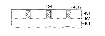
まず、図4Aに示すように、例えば単結晶シリコンなどの半導体材料からなる基板401の上に、シード層402を形成する。シード層402は、例えばTiからなる膜厚0.1μm程度の下層と、例えばAuからなる膜厚0.1μm程度の上層とを備えている。これらは、よく知られた蒸着法により形成することができる。このようにAuからなるシード層402を用いることで、後述するように、めっき法によりAuからなる金属パターンが形成可能である。また、チタンからなる下層は、金からなる上層と基板401との密着性を向上させるために備える。なお、基板401の表面に、例えば、酸化シリコン層(図示せず)を形成し、この上にシード層402を形成すればよい。
First, as shown in FIG. 4A, a
次に、シード層402の上に、公知のフォトリソグラフィ技術により、例えば、よく知られたポジ型のフォトレジスト材料からなる膜厚12μmのレジスト膜403を形成する。レジスト膜403は、所望の箇所に、シード層402に達する開口パターン403aを備える。また、図示しないが、基板401の周端部の領域に、レジスト膜403が無く、基板401が露出した露出部を形成する。
Next, a 12 μm-thick resist
次に、シード層402の露出している箇所に、Auより構成された金属パターン404を形成する。金属パターン404は、シード層402を一方の電極とする電解めっき法により、膜厚10μm程度にAuを堆積することで形成すればよい。例えば、Auめっき液に基板401を浸漬し、この中で、対向電極とシード層402との間に必要な電圧を印加することで、例えば、開口パターン403aに露出しているシード層402の上にAuを堆積することができる。このとき、基板401の外周部で露出しているシード層402に必要な配線を接続することで、シード層402に必要な電圧を印加すればよい。また、このめっきにより、前述した基板401の周端部の領域にも金属パターンが形成される。
Next, a
次に、レジスト膜403に対するエッチング処理を行い、図4Bに示すように、幅をより広くした開口パターン431aを備えるレジスト膜431形成し、金属パターン404とレジスト膜431の開口パターン431a内側壁との間に隙間が形成された状態とする。例えば、Nメチルピロリドンなどの剥離液を希釈した溶液を用いたウエットエッチングにより、上述したレジスト膜403の処理をすればよい。このとき、エッチング液に基板を浸漬して処理をするときに、超音波を印加し、開口パターン431aと金属パターン404との間に対する処理液の浸透性を向上させるようにしてもよい。また、酸素プラズマを用いた処理により、上述したレジスト膜403の処理をしてもよい。
Next, an etching process is performed on the resist
このように、本実施の形態では、金属パターン404が形成されている開口部を広げることで、金属パターン404側面も露出した状態としている。また、本実施の形態の場合、金属パターン404は、寸法が変化することがない。
Thus, in this embodiment, the side surface of the
次に、図4Cに示すように、開口部である開口パターン431aにおいて露出している金属パターン404の上面および側面に、例えば膜厚1μm程度の電着絶縁膜406を形成する。電着絶縁膜406の形成では、まず、電着を行うための電着液の中で、白金からなる対向電極に基板401の金属パターン404形成面を対向させて配置する。電着液には、例えば、エポキシ基を有するスルフォニウムイオン(カチオン)を電着成分として含むもの(日本ペイント株式会社;インシュリードINSULEED3020)を用いることができる。例えば、液温30℃として用いればよい。
Next, as shown in FIG. 4C, an
この状態で、定電圧源により、対向電極に正電圧を印加し、シード層402に負電圧を印加する。ここで、基板401の周端部のシード層に形成した金属パターンに必要な配線を接続することで、シード層402に対する負電圧の印加を行う。このようなカチオン電着により、金属パターン404の露出している面(上面および側面)に、電着液中の電着成分が付着(析出)し、電着絶縁膜406が形成される。
In this state, a positive voltage is applied to the counter electrode and a negative voltage is applied to the
以上のようにして電着絶縁膜406を形成した後、電着液の中より基板401を引き上げ、基板401を水洗処理して乾燥させた後、窒素雰囲気において110℃25分の加熱処理を行い、電着絶縁膜406を熱硬化する。加熱処理により、電着絶縁膜406は硬化し、また、電着絶縁膜406と金属パターン404との密着性が向上する。
After the
次に、レジスト膜431を除去することで、シード層402の上に、金属パターン404が形成され、金属パターン404の上面および側面に電着絶縁膜406が選択的に形成された状態が得られる。例えば、Nメチルピロリドンなどの剥離液を用いることで、レジスト膜431を除去すればよい。
Next, by removing the resist
この後、金属パターン404および電着絶縁膜406をマスクとしてシード層402をエッチング除去することで、図4Dに示すように、基板401の上で、金属パターン404毎に、シード層402を分離(絶縁分離)する。シード層402の上層の金層のエッチングには希王水を用い、下層のチタン層のエッチングにはフッ酸溶液を用いればよい。このエッチング処理において、金属パターン404は、電着絶縁膜406に覆われているため、エッチングされることがない。
Thereafter, by removing the
なお、本実施の形態4では、レジスト膜403をエッチングして幅をより広くした開口パターン431aを備えるレジスト膜431形成し、これにより、金属パターン404との間に間隙を形成したが、これに限るものではない。前述した実施の形態3を組み合わせ、レジストパターンのエッチングに加え、金属パターンのエッチングも行うことでこれらの間に間隙を形成するようにしてもよい。
In the fourth embodiment, the resist
また、基板を加熱(120℃)および冷却(−20℃)する工程を繰り返すことで、金属パターンとレジスト膜(開口パターン)との熱膨張率の違いにより、例えば、開口パターンをより広げることで、金属パターンの側面と開口パターンとの間に間隙を形成することもできる。また、レジスト膜を軟化点に近い温度にまで加熱することにより収縮させることで開口パターンをより広げ、金属パターンの側面と開口パターンとの間に間隙を形成してもよい。 Moreover, by repeating the process of heating (120 ° C.) and cooling (−20 ° C.) the substrate, the opening pattern is further widened due to the difference in thermal expansion coefficient between the metal pattern and the resist film (opening pattern), for example. A gap may be formed between the side surface of the metal pattern and the opening pattern. Further, the opening pattern may be further expanded by shrinking the resist film by heating it to a temperature close to the softening point, and a gap may be formed between the side surface of the metal pattern and the opening pattern.
[実施の形態5]
次に、本発明の実施の形態5について図5A〜図5Iを用いて説明する。図5A〜図5Iは、本実施の形態5におけるパターン形成方法を説明するための工程図である。実施の形態5では、本発明を多層配線構造の形成に適用した場合について説明する。
[Embodiment 5]
Next, Embodiment 5 of the present invention will be described with reference to FIGS. 5A to 5I. 5A to 5I are process diagrams for explaining the pattern forming method according to the fifth embodiment. In the fifth embodiment, the case where the present invention is applied to the formation of a multilayer wiring structure will be described.
まず、図5Aに示すように、例えば単結晶シリコンなどの半導体材料からなる基板501の上に、シード層502を形成する。シード層502は、例えばTiからなる膜厚0.1μm程度の下層と、例えばAuからなる膜厚0.1μm程度の上層とを備えている。これらは、よく知られた蒸着法により形成することができる。このようにAuからなるシード層502を用いることで、後述するように、めっき法によりAuからなる金属パターンが形成可能である。また、チタンからなる下層は、金からなる上層と基板501との密着性を向上させるために備える。なお、基板501の表面に、例えば、酸化シリコン層(図示せず)を形成し、この上にシード層502を形成すればよい。
First, as shown in FIG. 5A, a
次に、シード層502の上に、公知のフォトリソグラフィ技術により、例えば、よく知られたポジ型のフォトレジスト材料からなる膜厚12μmのレジスト膜503を形成する。レジスト膜503は、所望の箇所に、シード層502に達する開口パターン503aを備える。また、図示しないが、基板501の周端部の領域に、レジスト膜503が無く、基板501が露出した露出部を形成する。
Next, a 12 μm-thick resist
次に、シード層502の露出している箇所に、Auより構成された金属パターン504を形成する。金属パターン504は、シード層502を一方の電極とする電解めっき法により、膜厚10μm程度にAuを堆積することで形成すればよい。例えば、Auめっき液に基板501を浸漬し、この中で、対向電極とシード層502との間に必要な電圧を印加することで、例えば、開口パターン503aに露出しているシード層502の上にAuを堆積することができる。このとき、基板501の外周部で露出しているシード層502に必要な配線を接続することで、シード層502に必要な電圧を印加すればよい。また、このめっきにより、前述した基板501の周端部の領域にも金属パターンが形成される。
Next, a
次にレジスト膜503をマスクとして金属パターン504の上部および側部をエッチングし、図5Bに示すように、幅をより狭くした金属配線541を形成し、金属配線541とレジスト膜503の開口パターン503a内側壁との間に隙間が形成された状態とする。これにより、金属配線541は、上部(上面)に加え、側面も露出した状態となる。
Next, the upper and side portions of the
加えて、金属配線541の上面および側面に、例えば膜厚1μm程度の電着絶縁膜506を形成する。電着絶縁膜506の形成では、まず、電着を行うための電着液の中で、白金からなる対向電極に基板501の金属配線541形成面を対向させて配置する。電着液には、例えば、エポキシ基を有するスルフォニウムイオン(カチオン)を電着成分として含むもの(日本ペイント株式会社;インシュリードINSULEED3020)を用いることができる。例えば、液温30℃として用いればよい。
In addition, an
この状態で、定電圧源により、対向電極に正電圧を印加し、シード層502に負電圧を印加する。ここで、基板501の周端部のシード層に形成した金属パターンに必要な配線を接続することで、シード層502に対する負電圧の印加を行う。このようなカチオン電着により、金属配線541の露出している面(上面および側面)に、電着液中の電着成分が付着(析出)し、電着絶縁膜506が形成される。
In this state, a positive voltage is applied to the counter electrode and a negative voltage is applied to the
以上のようにして電着絶縁膜506を形成した後、電着液の中より基板501を引き上げ、基板501を水洗処理して乾燥させた後、窒素雰囲気において110℃25分の加熱処理を行い、電着絶縁膜506を熱硬化する。加熱処理により、電着絶縁膜506は硬化し、また、電着絶縁膜506と金属配線541との密着性が向上する。
After the
レジスト膜ターン503を除去することで、シード層502の上に、金属配線541が形成され、金属配線541の上面および側面に電着絶縁膜506が選択的に形成された状態が得られる。例えば、Nメチルピロリドンなどの剥離液を用いることで、レジスト膜503を除去すればよい。
By removing the resist
この後、電着絶縁膜506に対して190℃25分の加熱処理をさらに加え、硬化状態を促進させる。次に、金属配線541および電着絶縁膜506をマスクとしてシード層502をエッチング除去することで、図5Cに示すように、基板501の上で、金属配線541の下部にシード層502を分離(絶縁分離)する。シード層502の上層の金層のエッチングには希王水を用い、下層のチタン層のエッチングにはフッ酸溶液を用いればよい。このエッチング処理において、金属配線541は、電着絶縁膜506に覆われているため、エッチングされることがない。
Thereafter, a heat treatment at 190 ° C. for 25 minutes is further applied to the electrodeposited
加えて、電着絶縁膜506に覆われた金属配線541の上に、層間絶縁膜507を形成し、また、層間絶縁膜507に、金属配線541の上面の電着絶縁膜506に到達する開口部507aを形成する。例えば、新日鐵化学株式会社製のVPAシリーズアクリルポリマなど、感光性を有して200℃程度の加熱処理で硬化可能で、厚膜形成が可能な樹脂材料用いることで、層間絶縁膜507が形成可能である。
In addition, an
例えば、上記樹脂材料を金属配線541が形成された基板501の上に塗布して塗布膜を形成し、形成した塗布膜を公知のフォトリソグラフィ技術でパターニングして開口部507aを形成した後、当該パターンを熱硬化することで、層間絶縁膜507が形成できる。また、公知のSTP(Spin-coating film Transfer and hot Pressing)法により、上記樹脂材料の膜を形成してもよい。
For example, the resin material is applied onto the
本実施の形態によれば、金属配線541は、Auから構成されているが、層間絶縁膜507との間に電着絶縁膜506が介在しているので、これらの間で、良好な密着性が得られている。
According to the present embodiment, the
次に、上述したように形成した層間絶縁膜507をマスクとして、開口部507a内に露出している電着絶縁膜506をエッチング除去して開口パターン506aを形成し、図5Dに示すように、開口パターン506a,開口部507aの部分で金属配線541の表面(上面)を露出させる。
Next, using the
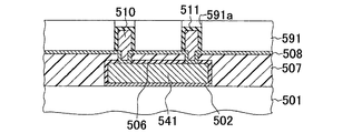
次に、図5Eに示すように、シード層508を形成する。シード層508は、例えばTiからなる膜厚0.1μm程度の下層と、例えばAuからなる膜厚0.1μm程度の上層とを備えている。これらは、シード層502と同様であり、よく知られた蒸着法により形成することができる。
Next, as shown in FIG. 5E, a
次に、シード層508の上に、公知のフォトリソグラフィ技術により、例えば、よく知られたポジ型のフォトレジスト材料からなる膜厚7μmのレジスト膜509を形成する。レジスト膜509は、所望の箇所に、シード層508に達する開口パターン509aを備える。また、図示しないが、基板501の周端部の領域の層間絶縁膜507の上に、レジスト膜509が無く、層間絶縁膜507が露出した露出部を形成する。
Next, a 7 μm-thick resist
次に、シード層508の露出している箇所に、Auより構成された金属パターン510を形成する。金属パターン510は、シード層508を一方の電極とする電解めっき法により、膜厚4μm程度にAuを堆積することで形成すればよい。例えば、Auめっき液に基板501を浸漬し、この中で、対向電極とシード層508との間に必要な電圧を印加することで、例えば、開口パターン509aに露出しているシード層508の上にAuを堆積することができる。このとき、基板501の外周部で露出しているシード層508に必要な配線を接続することで、シード層508に必要な電圧を印加すればよい。また、このめっきにより、前述した基板501の周端部の領域にも金属パターンが形成される。
Next, a
次に、レジスト膜509に対するエッチング処理を行い、図5Fに示すように、幅をより広くした開口パターン591aを備えるレジスト膜591形成し、金属パターン510とレジスト膜591の開口パターン591a内側壁との間に隙間が形成された状態とする。これにより、金属パターン510は、上部(上面)に加え、側面も露出した状態となる。また、本実施の形態の場合、金属パターン510は、寸法が変化することがない。
Next, an etching process is performed on the resist
次に、金属パターン510の上面および側面に、例えば膜厚1μm程度の電着絶縁膜511を形成する。電着絶縁膜511の形成は、前述した電着膜506の形成と同様である。
Next, an
次に、レジスト膜591を除去することで、図5Gに示すように、シード層508の上に、金属パターン510が形成され、金属パターン510の上面および側面に電着絶縁膜511が選択的に形成された状態が得られる。例えば、Nメチルピロリドンなどの剥離液を用いることで、レジスト膜591を除去すればよい。
Next, by removing the resist
この後、金属パターン510および電着絶縁膜511をマスクとしてシード層508をエッチング除去することで、層間絶縁膜507の上で、金属パターン510毎に、シード層508を分離(絶縁分離)する。シード層508の上層の金層のエッチングには希王水を用い、下層のチタン層のエッチングにはフッ酸溶液を用いればよい。このエッチング処理において、金属パターン510は、電着絶縁膜511に覆われているため、エッチングされることがない。
Thereafter, the
次に、図5Hに示すように、電着絶縁膜511に覆われた金属パターン510の上に、層間絶縁膜512を形成し、また、層間絶縁膜512に、金属パターン510の上面の電着絶縁膜511に到達する開口部512aを形成する。層間絶縁膜512は、層間絶縁膜507と同様に形成すればよい。ここで、本実施の形態によれば、金属パターン510は、Auから構成されているが、層間絶縁膜512との間に電着絶縁膜511が介在しているので、これらの間で、良好な密着性が得られている。
Next, as shown in FIG. 5H, an
次に、層間絶縁膜512をマスクとして、開口部512a内に露出している電着絶縁膜511をエッチング除去し、開口部512aの部分で金属パターン510の表面(上面)を露出させる。
Next, using the
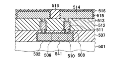
次に、図5Iに示すように、シード層513を形成し、金属配線514を形成し、金属配線514を被覆する電着絶縁膜515を形成し、これらの上に保護絶縁膜516を形成する。シード層513は、シード層508と同様に形成すればよい。また、金属配線514は、金属配線541と同様に形成すればよい。また、電着絶縁膜515は、電着絶縁膜506と同様に形成すればよい。
Next, as shown in FIG. 5I, a
上述した本実施の形態によれば、金属配線541を備える配線層の上に、金属パターン510をビアとして金属配線541に接続する金属配線514を備える配線層が積層された多層配線構造が構成できる。また、金属配線541,514および金属パターン510をAuから構成しているが、これらは、良好な密着性を備える電着絶縁膜で被覆されているので、層間絶縁膜の剥がれなどを抑制することができる。
According to this embodiment described above, a multilayer wiring structure in which a wiring layer including a
ところで、上述では、カチオンを電着成分としたカチオン電着を例に説明したが、これに限るものではない。例えば、ポリイミド系の有機成分およびカルボキシルイオン(アニオン)を電着成分として含むものを用いたアニオン電着により、電着膜を形成するようにしてもよい(非特許文献1参照)。この場合、例えばめっきにより形成したCuよりなる金属パターンに、選択的に電着膜を形成することができる。 In the above description, cation electrodeposition using cations as electrodeposition components has been described as an example. However, the present invention is not limited to this. For example, the electrodeposition film may be formed by anion electrodeposition using a polyimide-based organic component and a carboxyl ion (anion) as an electrodeposition component (see Non-Patent Document 1). In this case, for example, an electrodeposition film can be selectively formed on a metal pattern made of Cu formed by plating.
また、上述では、金属材料としてAuを用いたが、これに限るものではなく、Cuや他の金属材料を用いるようにしてもよい。用いる金属材料に対応させて、電着に用いる電着液などの材料を適宜に選択すればよい。また、シード層としてAu/Tiの積層膜を用いたが、これに限るものではなく、金属材料としてAuを用いる場合、Au/Crのシード層を用いてもよい。また、Cu/Cr,Cu/Ti,あるいはSUSやFeなどの金属を用いるようにしてもよい。 In the above description, Au is used as the metal material. However, the present invention is not limited to this, and Cu or another metal material may be used. A material such as an electrodeposition liquid used for electrodeposition may be appropriately selected in accordance with the metal material to be used. Further, although the Au / Ti laminated film is used as the seed layer, the present invention is not limited to this. When Au is used as the metal material, an Au / Cr seed layer may be used. Further, Cu / Cr, Cu / Ti, or a metal such as SUS or Fe may be used.
101…基板、101a…周端部、102…シード層、103…レジスト膜、103a…開口パターン、104…金属パターン、105…金属パターン、106…電着絶縁膜、141…金属パターン、151…容器、152…電着液、153…対向電極、154…定電圧源。
DESCRIPTION OF
Claims (10)
前記シード層の上に開口パターンを備えたレジスト膜を形成する工程と、
前記開口パターンに露出する前記シード層の上にめっきにより金属パターンを形成する工程と、
前記シード層に電圧を印加する電着により、前記金属パターンの一部が露出する開口部において露出している前記金属パターンの表面に電着膜を形成する工程と、
前記レジスト膜を除去する工程と、
前記金属パターンをマスクとして前記シード層を選択的にエッチングして分離する工程と
を少なくとも備えることを特徴とするパターン形成方法。 Forming a seed layer made of metal on a substrate;
Forming a resist film having an opening pattern on the seed layer;
Forming a metal pattern by plating on the seed layer exposed to the opening pattern;
Forming an electrodeposition film on the surface of the metal pattern exposed in an opening where a part of the metal pattern is exposed by electrodeposition applying a voltage to the seed layer;
Removing the resist film;
And a step of selectively etching and separating the seed layer using the metal pattern as a mask.
前記電着膜を形成するときの前記開口部は、前記レジスト膜の前記開口パターンである
ことを特徴とするパターン形成方法。 In the pattern formation method of Claim 1,
The pattern forming method, wherein the opening when forming the electrodeposition film is the opening pattern of the resist film.
前記電着膜を形成するときの前記開口部は、前記レジスト膜を除去して新たに形成したレジスト膜に形成した新たな開口パターンである
ことを特徴とするパターン形成方法。 In the pattern formation method of Claim 1,
The pattern forming method, wherein the opening when forming the electrodeposition film is a new opening pattern formed in a resist film newly formed by removing the resist film.
前記金属パターンを形成した後、前記開口部の側面と前記金属パターンとの間に隙間を形成して前記金属パターンの上面および側面を露出させ、
前記金属パターンの露出している上面および側面に前記電着膜を形成する
ことを特徴とするパターン形成方法。 In the pattern formation method of any one of Claims 1-3,
After forming the metal pattern, a gap is formed between the side surface of the opening and the metal pattern to expose the upper surface and the side surface of the metal pattern,
The pattern forming method, wherein the electrodeposition film is formed on the exposed upper surface and side surfaces of the metal pattern.
前記金属パターンを形成した後、前記金属パターンをエッチングすることで、前記開口部の側面と前記金属パターンとの間に隙間を形成して前記金属パターンの上面および側面を露出させる
ことを特徴とするパターン形成方法。 In the pattern formation method of Claim 4,
After the metal pattern is formed, the metal pattern is etched to form a gap between the side surface of the opening and the metal pattern to expose the upper surface and the side surface of the metal pattern. Pattern forming method.
前記金属パターンを形成した後、前記開口部を広げることで、前記開口部の側面と前記金属パターンとの間に隙間を形成して前記金属パターンの上面および側面を露出させる
ことを特徴とするパターン形成方法。 In the pattern formation method of Claim 4,
After the metal pattern is formed, the opening is widened to form a gap between the side surface of the opening and the metal pattern to expose the upper surface and the side surface of the metal pattern. Forming method.
前記シード層を選択的にエッチングして分離した後、前記金属パターンの前記電着膜で被覆されていない側面をエッチングする工程を新たに備える
ことを特徴とするパターン形成方法。 In the pattern formation method of any one of Claims 1-3,
After the seed layer is selectively etched and separated, the pattern forming method further includes a step of etching a side surface of the metal pattern not covered with the electrodeposition film.
前記シード層および金属パターンの一部は、前記基板の上に形成した犠牲パターン上に形成し、
前記金属パターンをマスクとして前記シード層を選択的にエッチングして分離した後、前記犠牲パターンを除去し、前記シード層および金属パターンの一部で、前記基板の上に可動構造体を形成する
ことを特徴とするパターン形成方法。 In the pattern formation method of Claim 7,
A part of the seed layer and the metal pattern is formed on a sacrificial pattern formed on the substrate;
The seed layer is selectively etched and separated using the metal pattern as a mask, the sacrificial pattern is removed, and a movable structure is formed on the substrate with the seed layer and a part of the metal pattern. A pattern forming method characterized by the above.
前記電着膜で覆われた前記金属パターンを覆う絶縁膜を形成する工程を新たに備える
ことを特徴とするパターン形成方法。 In the pattern formation method of any one of Claims 4-6,
The pattern formation method characterized by newly providing the process of forming the insulating film which covers the said metal pattern covered with the said electrodeposition film.
前記電着に用いる電着液は、スルフォニウムイオンを電着成分として含んでいる
ことを特徴とするパターン形成方法。 In the pattern formation method of any one of Claims 1-9,
The electrodeposition liquid used for the said electrodeposition contains sulfonium ion as an electrodeposition component. The pattern formation method characterized by the above-mentioned.
Priority Applications (1)
| Application Number | Priority Date | Filing Date | Title |
|---|---|---|---|
| JP2008200550A JP2010040693A (en) | 2008-08-04 | 2008-08-04 | Method for forming pattern |
Applications Claiming Priority (1)
| Application Number | Priority Date | Filing Date | Title |
|---|---|---|---|
| JP2008200550A JP2010040693A (en) | 2008-08-04 | 2008-08-04 | Method for forming pattern |
Publications (1)
| Publication Number | Publication Date |
|---|---|
| JP2010040693A true JP2010040693A (en) | 2010-02-18 |
Family
ID=42012942
Family Applications (1)
| Application Number | Title | Priority Date | Filing Date |
|---|---|---|---|
| JP2008200550A Pending JP2010040693A (en) | 2008-08-04 | 2008-08-04 | Method for forming pattern |
Country Status (1)
| Country | Link |
|---|---|
| JP (1) | JP2010040693A (en) |
Cited By (4)
| Publication number | Priority date | Publication date | Assignee | Title |
|---|---|---|---|---|
| JP2015225650A (en) * | 2014-05-28 | 2015-12-14 | 介面光電股▲ふん▼有限公司JTOUCH Corporation | Microstructure manufacturing method of metal wiring |
| KR20180001666A (en) * | 2016-06-24 | 2018-01-05 | 에이피시스템 주식회사 | A Method for Manufacturing a Fine Metal Mask Using Electroplating |
| CN108573851A (en) * | 2017-03-08 | 2018-09-25 | 上海新昇半导体科技有限公司 | The preparation method of autoregistration seed layer and autoregistration film |
| JP2020030448A (en) * | 2018-08-20 | 2020-02-27 | 地方独立行政法人大阪産業技術研究所 | Capacitive touch sensor and manufacturing method thereof |
-
2008
- 2008-08-04 JP JP2008200550A patent/JP2010040693A/en active Pending
Cited By (5)
| Publication number | Priority date | Publication date | Assignee | Title |
|---|---|---|---|---|
| JP2015225650A (en) * | 2014-05-28 | 2015-12-14 | 介面光電股▲ふん▼有限公司JTOUCH Corporation | Microstructure manufacturing method of metal wiring |
| KR20180001666A (en) * | 2016-06-24 | 2018-01-05 | 에이피시스템 주식회사 | A Method for Manufacturing a Fine Metal Mask Using Electroplating |
| KR102081191B1 (en) * | 2016-06-24 | 2020-02-26 | 에이피시스템 주식회사 | A Method for Manufacturing a Fine Metal Mask Using Electroplating |
| CN108573851A (en) * | 2017-03-08 | 2018-09-25 | 上海新昇半导体科技有限公司 | The preparation method of autoregistration seed layer and autoregistration film |
| JP2020030448A (en) * | 2018-08-20 | 2020-02-27 | 地方独立行政法人大阪産業技術研究所 | Capacitive touch sensor and manufacturing method thereof |
Similar Documents
| Publication | Publication Date | Title |
|---|---|---|
| JP5097172B2 (en) | Graphene layer peeling method, graphene wafer manufacturing method, and graphene element manufacturing method | |
| US10629744B2 (en) | Electronic device and method for fabricating the same | |
| US9177821B2 (en) | Method of fabricating electronic circuit | |
| CN101950644A (en) | Manufacturing method of flexible heat-sensitive thin film resistor array | |
| JP2010040693A (en) | Method for forming pattern | |
| TWI459520B (en) | Adapter plate and forming method thereof | |
| KR20130106836A (en) | Substrate sheet | |
| JP2004311713A (en) | Mold for manufacturing semiconductor devices | |
| TWI683357B (en) | Semiconductor apparatus manufacturing method | |
| JP2018181953A (en) | Method of manufacturing through electrode substrate and through electrode substrate | |
| JP7110189B2 (en) | Formation of delayed vias in electronic devices | |
| WO2015107796A1 (en) | Semiconductor element and method for producing same, and semiconductor device | |
| JP5279731B2 (en) | Manufacturing method of electric circuit on ultra-thin plastic film | |
| US20110274829A1 (en) | Method for producing a flexible circuit configuration | |
| JP3706310B2 (en) | Microstructure manufacturing method | |
| TW202025870A (en) | Circuit board and method for making the same | |
| JP6028887B2 (en) | Wiring board, infrared sensor, and through electrode forming method | |
| KR100975628B1 (en) | Method for manufacturing a thin film flexible thermoelectric module using peeling process | |
| CN112786513B (en) | A kind of processing method of thin film device and thin film device | |
| CN112786515B (en) | Processing method of thin film device | |
| JP2005123358A (en) | Manufacturing method of wafer batch type bumped membrane | |
| JPS61251153A (en) | Formation of bump of semiconductor device | |
| JP2011210939A (en) | Semiconductor device and method of manufacturing semiconductor device | |
| KR100734664B1 (en) | Fine pattern formation method using the orientation principle of the Langmuir blowjet film | |
| JP2025114297A (en) | Semiconductor device manufacturing method and semiconductor device |