JP2009105427A - Manufacturing method of semiconductor substrate - Google Patents
Manufacturing method of semiconductor substrate Download PDFInfo
- Publication number
- JP2009105427A JP2009105427A JP2008325864A JP2008325864A JP2009105427A JP 2009105427 A JP2009105427 A JP 2009105427A JP 2008325864 A JP2008325864 A JP 2008325864A JP 2008325864 A JP2008325864 A JP 2008325864A JP 2009105427 A JP2009105427 A JP 2009105427A
- Authority
- JP
- Japan
- Prior art keywords
- layer
- substrate
- sige
- lattice
- sige layer
- Prior art date
- Legal status (The legal status is an assumption and is not a legal conclusion. Google has not performed a legal analysis and makes no representation as to the accuracy of the status listed.)
- Abandoned
Links
Images


Classifications
-
- H—ELECTRICITY
- H10—SEMICONDUCTOR DEVICES; ELECTRIC SOLID-STATE DEVICES NOT OTHERWISE PROVIDED FOR
- H10D—INORGANIC ELECTRIC SEMICONDUCTOR DEVICES
- H10D30/00—Field-effect transistors [FET]
- H10D30/60—Insulated-gate field-effect transistors [IGFET]
- H10D30/67—Thin-film transistors [TFT]
- H10D30/6757—Thin-film transistors [TFT] characterised by the structure of the channel, e.g. transverse or longitudinal shape or doping profile
-
- H—ELECTRICITY
- H10—SEMICONDUCTOR DEVICES; ELECTRIC SOLID-STATE DEVICES NOT OTHERWISE PROVIDED FOR
- H10D—INORGANIC ELECTRIC SEMICONDUCTOR DEVICES
- H10D30/00—Field-effect transistors [FET]
- H10D30/01—Manufacture or treatment
- H10D30/021—Manufacture or treatment of FETs having insulated gates [IGFET]
- H10D30/031—Manufacture or treatment of FETs having insulated gates [IGFET] of thin-film transistors [TFT]
-
- H—ELECTRICITY
- H10—SEMICONDUCTOR DEVICES; ELECTRIC SOLID-STATE DEVICES NOT OTHERWISE PROVIDED FOR
- H10D—INORGANIC ELECTRIC SEMICONDUCTOR DEVICES
- H10D30/00—Field-effect transistors [FET]
- H10D30/60—Insulated-gate field-effect transistors [IGFET]
- H10D30/67—Thin-film transistors [TFT]
- H10D30/674—Thin-film transistors [TFT] characterised by the active materials
- H10D30/6741—Group IV materials, e.g. germanium or silicon carbide
- H10D30/6748—Group IV materials, e.g. germanium or silicon carbide having a multilayer structure or superlattice structure
-
- H—ELECTRICITY
- H10—SEMICONDUCTOR DEVICES; ELECTRIC SOLID-STATE DEVICES NOT OTHERWISE PROVIDED FOR
- H10D—INORGANIC ELECTRIC SEMICONDUCTOR DEVICES
- H10D30/00—Field-effect transistors [FET]
- H10D30/60—Insulated-gate field-effect transistors [IGFET]
- H10D30/751—Insulated-gate field-effect transistors [IGFET] having composition variations in the channel regions
-
- H—ELECTRICITY
- H10—SEMICONDUCTOR DEVICES; ELECTRIC SOLID-STATE DEVICES NOT OTHERWISE PROVIDED FOR
- H10D—INORGANIC ELECTRIC SEMICONDUCTOR DEVICES
- H10D30/00—Field-effect transistors [FET]
- H10D30/60—Insulated-gate field-effect transistors [IGFET]
- H10D30/67—Thin-film transistors [TFT]
- H10D30/674—Thin-film transistors [TFT] characterised by the active materials
- H10D30/675—Group III-V materials, Group II-VI materials, Group IV-VI materials, selenium or tellurium
Landscapes
- Thin Film Transistor (AREA)
- Recrystallisation Techniques (AREA)
Abstract
【課題】
歪み層/歪み印加結晶層構造において、歪み印加結晶層構造より発生する結晶欠陥によ
る歪み層の結晶性劣化を低減し、かつ絶縁層上に歪み層/歪み印加結晶層構造を薄膜で形
成した基板の形成方法を提供する。
【解決手段】
Si基板上の絶縁層と、別の半導体基板上のSiGe層とを、半導体張り合わせ技術を
用いて接合し、SiGe層側の半導体基板を研磨等により除去する。
【選択図】 図9【Task】
In a strained layer / strain-applying crystal layer structure, a substrate in which the crystallinity deterioration of the strained layer due to crystal defects generated from the strain-applying crystal layer structure is reduced and the strain layer / strain-applying crystal layer structure is formed as a thin film on the insulating layer A forming method is provided.
[Solution]
The insulating layer on the Si substrate and the SiGe layer on another semiconductor substrate are joined using a semiconductor bonding technique, and the semiconductor substrate on the SiGe layer side is removed by polishing or the like.
[Selection] Figure 9
Description
本発明は、半導体基板、とりわけ歪みSi層を活性領域とする半導体装置に用いる半導
体基板の製造方法に関する。
The present invention relates to a method of manufacturing a semiconductor substrate, particularly a semiconductor substrate used in a semiconductor device having a strained Si layer as an active region.
Si半導体素子、とりわけMOSFETトランジスタの性能は、大規模集積回路(LS
I)の進歩と共に年々向上している。しかしながら、近年リソグラフィ技術の微細化への
限界、Siの理論的移動度へのキャリア移動度への接近などが指摘され、MOSFETの
さらなる高性能化への困難さが増している。
The performance of Si semiconductor devices, especially MOSFET transistors, is large-scale integrated circuits (LS
It improves year by year with the progress of I). However, in recent years, limitations to lithography technology miniaturization, approach to carrier mobility to the theoretical mobility of Si, etc. have been pointed out, and the difficulty in further increasing the performance of MOSFETs has increased.
また、一般に半導体素子の高性能化への施策として、例えばSiよりも理論的移動度の
速いGaAs半導体結晶やSiC半導体結晶などのSiとは異なる結晶を用いてより高性
能化を実現する方法が検討されている。
In general, as a measure for improving the performance of a semiconductor device, there is a method for realizing higher performance by using a crystal different from Si, such as a GaAs semiconductor crystal or SiC semiconductor crystal having a theoretical mobility faster than that of Si. It is being considered.
しかしながらGaAs半導体結晶やSiC結晶では、現在多く用いられているSiデバ
イスの製造プロセスとの混在が困難であるため、素子開発に多大な時間と労力が必要であ
り、実際に大量生産を行う場合には製造ラインの完全な見直しや置き換えが要求される。
However, GaAs semiconductor crystals and SiC crystals are difficult to mix with Si device manufacturing processes that are widely used at present, so a great deal of time and effort is required for element development. Requires a complete review and replacement of the production line.
そこで、現在多く用いられているSiデバイス製造プロセス技術や製造装置のノウハウ
を生かしつつ、より短い開発期間、より低い投資効率で実現可能な高性能Si系半導体素
子の開発が切望されている。
Therefore, development of a high-performance Si-based semiconductor element that can be realized with a shorter development period and lower investment efficiency while making full use of the Si device manufacturing process technology and manufacturing equipment know-how that are currently widely used is eagerly desired.
このために、Siの電子移動度を向上させSi−MOSFETを高性能化する研究が行
われている。Siの移動度を向上させる方法のひとつとしてSi層に歪みを印加する技術
が注目されている。一般に半導体層に歪みを印加すると、そのバンド構造が変化し、チャ
ネル中のキャリアの散乱が抑制されるため電子移動度の向上が期待できる。
For this reason, research has been conducted on improving the electron mobility of Si and improving the performance of Si-MOSFETs. As one of the methods for improving the mobility of Si, a technique for applying strain to the Si layer has attracted attention. In general, when strain is applied to a semiconductor layer, the band structure is changed, and scattering of carriers in the channel is suppressed, so that an improvement in electron mobility can be expected.
具体的には、Si基板上にSiよりも格子定数の大きな材料からなる混晶層、例えばG
eを20atm%含むSiGe混晶層(以下、単にSiGe層という)を格子緩和するよ
うに厚く(数μm)形成し、この格子緩和SiGe層上に薄いSi層(数nm)を形成す
ると、SiGeとSiの格子定数の差によって歪みのかかった歪Si層が形成される。
Specifically, a mixed crystal layer made of a material having a larger lattice constant than Si on the Si substrate, for example, G
When a SiGe mixed crystal layer containing 20 atm% of e (hereinafter referred to simply as a SiGe layer) is formed thick (several μm) so as to be lattice-relaxed, and a thin Si layer (several nm) is formed on this lattice-relaxed SiGe layer, A strained Si layer is formed due to the difference in lattice constant between Si and Si.
このような歪Si層をMOSFETのチャネルに用いると、歪みのないSi層をチャネ
ルに用いた場合の約1.76倍と大幅な電子移動度の向上を達成できることが報告されて
いる。(例えば非特許文献1参照)
また、Siの電子移動度を向上させる別の方法として、MOSFETのチャネル長をよ
り短くする短チャネル化の方法がある。しかしながら短チャネル化をすすめると浮遊容量
の影響が大きくなるため、期待通りに電子移動度を向上することが困難になる。
It has been reported that when such a strained Si layer is used for a channel of a MOSFET, a significant improvement in electron mobility can be achieved, which is about 1.76 times that when an unstrained Si layer is used for a channel. (For example, see Non-Patent Document 1)
As another method for improving the electron mobility of Si, there is a method for shortening the channel length of the MOSFET. However, if the channel length is shortened, the effect of stray capacitance increases, and it becomes difficult to improve the electron mobility as expected.
これを解決するため、Si基板上に絶縁膜を介してSi層を形成したSOI(sili
con on insulator)層中にチャネル層を設ける構造が注目されている。こ
の構造では絶縁膜により完全にアイソレーションされるので、浮遊容量の低減や素子分離
が容易となり、さらなる低消費電力化、高集積化が実現すると期待されている。
In order to solve this problem, an SOI (sili) in which a Si layer is formed on an Si substrate via an insulating film.
A structure in which a channel layer is provided in a (con on insulator) layer has attracted attention. Since this structure is completely isolated by the insulating film, it is expected that the stray capacitance can be reduced and the element can be easily separated, and further lower power consumption and higher integration can be realized.
そこで電子移動度の向上を期待できる歪Si層を、浮遊容量の低減や素子分離が容易と
なるSOI構造に適用した半導体素子構造に適用する試みがされてきた。図1を参照しこ
の構造について説明する。
Therefore, attempts have been made to apply a strained Si layer that can be expected to improve electron mobility to a semiconductor element structure applied to an SOI structure that facilitates reduction of stray capacitance and element isolation. This structure will be described with reference to FIG.
先ず、図1Aに示すように、予めSi基板1上にSiO2絶縁膜2と10nm〜30n
mのSOI層3が形成されたSOI基板を準備し、このSOI基板上にSiより格子定数
の大きいGe濃度20%のSiGe層4をSOI層3よりも十分厚く形成する。
First, as shown in FIG. 1A, the SiO 2
An SOI substrate on which an
次に、図1Bに示すように、窒素雰囲気中で1100℃のアニールを1時間施すことに
よってSiGe層4からSOI層3に印加された引っ張り歪み(STRAIN)によって
、SOI層3が塑性変形し格子緩和する。同時にSiGe層4も格子緩和する。この塑性
変形によってSOI層3中には貫通転位やミスフィット転位などの転位33が発生する。
Next, as shown in FIG. 1B, the
次に、格子緩和SiGe層4上に薄膜のSiを形成することによって、引っ張り歪みを
有する歪Si層5を形成できる。
Next, by forming a thin Si film on the lattice-
従来SOI層3中に発生する転位33の大部分は、格子緩和したSOI層3中に生じ、
かつこの層中に閉じこめられるため、格子緩和SiGe層4中には伝搬しないと考えられ
てきた。
Most of the
In addition, since it is confined in this layer, it has been considered that it does not propagate into the lattice
しかしながら、格子緩和のために窒素雰囲気中で1時間1100℃の条件でアニールを
施すと1個/10μm2程度の密度で、SiGe層4の表面にも伝播し、この欠陥が歪S
i層5の結晶性を劣化させることが分かった。この後の歪Si層5にMOSFET等の半
導体素子を形成するのであるが、歪Si層5の結晶性の劣化は半導体素子の特性を大きく
劣化させる可能性がある。このことは半導体素子が微細化されるほど顕著になると予想さ
れる。
However, when annealing is performed in a nitrogen atmosphere for 1 hour at 1100 ° C. to relax the lattice, it propagates to the surface of the
It was found that the crystallinity of the
また、SiGe層4を格子緩和させるときに生じた欠陥は、この後のゲート、電極など
の形成プロセスやイオンドーピング後の結晶性回復アニールなどの高温処理過程でも増幅
する場合があり、さらに歪Si層5の結晶性を劣化させる可能性がある。
In addition, defects generated when the lattice relaxation of the
SOI層3に発生し格子緩和させるための転位33をSiGe表面に伝播させないため
にはSiGe層4を数μm以上形成しなければならない。
In order to prevent
しかしながら浮遊容量の影響を抑えるといったSOI基板構造の効果を十分に発揮する
ためにはSiO2絶縁層2からチャネル層である歪Si層5までの厚みを極力抑えること
が必要である。したがって数μmのSiGe層4を形成しなければならないこの方法では
SOI基板構造の効果を十分発揮できない。
上述したように、従来の方法では、SOI基板上に形成されるチャネル層となる歪Si
層を備えた半導体デバイスは、欠陥を抑えるためにはSOI基板絶縁膜上の膜厚が厚くな
り、SOI基板絶縁膜上の膜厚を薄く形成すれば欠陥が増幅するという問題を有している
。
As described above, in the conventional method, strained Si that becomes a channel layer formed on the SOI substrate is used.
A semiconductor device having a layer has a problem that the film thickness on the SOI substrate insulating film is increased in order to suppress defects, and the defect is amplified if the film thickness on the SOI substrate insulating film is formed thin. .
そこで本発明は、SOI基板絶縁層上の膜厚の薄膜化およびチャネル層となる歪層の欠
陥の低減を両立でき、十分な歪みをチャネル層に印加し、より高性能な半導体素子を低コ
ストに形成できる半導体基板の製造方法を提供することを目的とする。
Therefore, the present invention can achieve both a reduction in the thickness of the SOI substrate insulating layer and a reduction in defects in the strained layer serving as the channel layer, while applying sufficient strain to the channel layer to reduce the cost of a higher performance semiconductor device. It is an object of the present invention to provide a method for manufacturing a semiconductor substrate that can be formed in a simple manner.
上記目的を達成するために、
本発明の第1の半導体基板の製造方法は、
第1のSi基板上に絶縁膜を形成する工程と、
第2のSi基板上に、SiGeバッファ層、第1の格子緩和SiGe層、歪Si層およ
び第2の格子緩和SiGe層の積層を順に形成する工程と、
前記第1のSi基板上に形成された絶縁膜と、前記第2のSi基板上に形成された第2
の格子緩和SiGe層と、を貼り合わせる工程と、
前記第2のSi基板、前記SiGeバッファ層、前記第1の格子緩和SiGe層を除去
して、前記第1のSi基板、前記絶縁膜、前記第2の格子緩和SiGe層および前記歪S
i層の積層を形成する工程と、
を具備することを特徴とする。
To achieve the above objective,
The manufacturing method of the first semiconductor substrate of the present invention,
Forming an insulating film on the first Si substrate;
Forming a stack of an SiGe buffer layer, a first lattice relaxed SiGe layer, a strained Si layer, and a second lattice relaxed SiGe layer on the second Si substrate in order;
An insulating film formed on the first Si substrate; and a second film formed on the second Si substrate.
Bonding the lattice relaxed SiGe layer,
The second Si substrate, the SiGe buffer layer, and the first lattice relaxed SiGe layer are removed, and the first Si substrate, the insulating film, the second lattice relaxed SiGe layer, and the strain S are removed.
forming a stack of i layers;
It is characterized by comprising.
前記第1の半導体基板の製造方法において、前記SiGeバッファ層は膜厚方向にGe
濃度勾配があり、前記第2のSi基板側から遠ざかるに従ってGe濃度が徐々に高くなる
ことが望ましい。
In the method for manufacturing the first semiconductor substrate, the SiGe buffer layer is formed in a Ge direction in a film thickness direction.
It is desirable that there is a concentration gradient, and that the Ge concentration gradually increases as the distance from the second Si substrate side increases.
また、本発明の第2の半導体基板の製造方法は、
Si基板上に第1の絶縁膜を形成する工程と、
SiGe基板上に、第1の格子緩和SiGe層、歪Si層、第2の格子緩和SiGe層
および第2の絶縁膜を順次形成する工程と、
前記Si基板上に形成された第1の絶縁膜と、前記SiGe基板上に形成された第2の
絶縁膜と、を貼り合わせる工程と、
前記SiGe基板および前記第1の格子緩和SiGe層を除去して、前記Si基板、前
記第1および第2の絶縁膜、前記第2の格子緩和SiGe層ならびに前記歪Si層の積層
を形成する工程と、
を具備することを特徴とする半導体基板の製造方法である。
The second method for manufacturing a semiconductor substrate of the present invention includes:
Forming a first insulating film on the Si substrate;
Forming a first lattice-relaxed SiGe layer, a strained Si layer, a second lattice-relaxed SiGe layer, and a second insulating film on the SiGe substrate sequentially;
Bonding the first insulating film formed on the Si substrate and the second insulating film formed on the SiGe substrate;
Removing the SiGe substrate and the first lattice relaxed SiGe layer to form a stack of the Si substrate, the first and second insulating films, the second lattice relaxed SiGe layer, and the strained Si layer; When,
A method for manufacturing a semiconductor substrate, comprising:
また、本発明の第3の半導体基板の製造方法は、
第1のSi基板上に絶縁膜を形成する工程と、
第2のSi基板上に、SiGeバッファ層と、前記SiGeバッファ層上に形成された
格子緩和SiGe層とを形成する工程と、
前記第1のSi基板上に形成された絶縁膜と、前記第2のSi基板上に形成された格子
緩和SiGe層と、を貼り合わせる工程と、
前記第2のSi基板、前記SiGeバッファ層を除去して、前記第1のSi基板、前記
絶縁膜及び前記格子緩和SiGe層、の積層を形成する工程と、
前記格子緩和SiGe層上に、引っ張り格子歪が印加されたSi層を形成する工程と、
を具備することを特徴とする半導体基板の製造方法である。
Further, the third method for manufacturing a semiconductor substrate of the present invention,
Forming an insulating film on the first Si substrate;
Forming a SiGe buffer layer and a lattice relaxation SiGe layer formed on the SiGe buffer layer on a second Si substrate;
Bonding the insulating film formed on the first Si substrate and the lattice relaxed SiGe layer formed on the second Si substrate;
Removing the second Si substrate and the SiGe buffer layer to form a stack of the first Si substrate, the insulating film and the lattice-relaxed SiGe layer;
Forming a Si layer to which a tensile lattice strain is applied on the lattice-relaxed SiGe layer;
A method for manufacturing a semiconductor substrate, comprising:
本発明によれば、従来困難であった、ストレッサとしての歪み層から伝搬する欠陥によ
るデバイス層の結晶性劣化が低減されると共に、SOI構造上の絶縁層上の合計厚みをよ
り薄くすることが可能である。従って、素子特性の劣化を抑え、低消費電力化、高集積化
が可能となり、半導体素子の高性能化が実現できる。
According to the present invention, crystallinity deterioration of a device layer due to defects propagated from a strained layer as a stressor, which has been difficult in the past, is reduced, and the total thickness on the insulating layer on the SOI structure can be made thinner. Is possible. Therefore, deterioration of element characteristics can be suppressed, low power consumption and high integration can be achieved, and high performance of the semiconductor element can be realized.
以下、図面を参照しながら、本発明の実施の形態(以下、実施形態という)を説明する
。
(第1の実施形態)
図3は本発明の第1の実施例に係る半導体基板の製造方法を説明するための半導体基板
の断面図である。
Hereinafter, embodiments of the present invention (hereinafter referred to as embodiments) will be described with reference to the drawings.
(First embodiment)
FIG. 3 is a cross-sectional view of a semiconductor substrate for explaining a method of manufacturing a semiconductor substrate according to the first embodiment of the present invention.
先ず、図3Aに示すように、Si基板1上に予めSi酸化膜2を形成する。Si酸化膜
2は、dry酸化膜、wet酸化膜等の熱酸化膜やCVD(Chemical Vapo
r Deposition)膜、溶液処理によるwet酸化膜など広く用いられる方法で
形成できる。
First, as shown in FIG. 3A, a
r Deposition) film, wet oxide film by solution processing, and the like can be used.
次に、図3Bに示すように、別のSi基板21上に予めSiGe層4を形成する。Si
Ge層4は基本的にはアンドープとされる。またSiGe層4は少なくともSi基板21
側のGe組成が100atm%未満、表面側のGe組成が0atm%より大きいことが必
要である。さらにSiGe層4は高性能化のために30atm%より大、少なくともSi
基板21側のGe組成を30atm%より大とすることが望ましい。Ge組成を30at
m%より大きくすると、歪Si層における電子移動度を高くすることができるからである
。一方、SiGe層4のGe組成は80atm%以下であることが望ましい。
Next, as shown in FIG. 3B, a
The
It is necessary that the Ge composition on the side is less than 100 atm% and the Ge composition on the surface side is greater than 0 atm%. Further, the
It is desirable that the Ge composition on the
This is because if it is larger than m%, the electron mobility in the strained Si layer can be increased. On the other hand, the Ge composition of the
SiGe層4は、CVD(Chemical Vapor Deposition)、M
BE(Molecular Beam Epitaxy)、スパッタープロセスなどにより
形成することができる。SiGe層4をCVDで形成する場合は、Siの原材料ガスとG
eの原材料ガスを、例えば550℃に加熱したSi基板21上に導入して積層する。
The
It can be formed by BE (Molecular Beam Epitaxy), a sputtering process, or the like. When the
The raw material gas e is introduced and stacked on the
次に、Si酸化膜2の上面2sとSiGe層4の上面4sを合わせて、基板1と21を
張り合わせる。張り合わせ方法の一例としては、数百度(例えば400〜700℃)程度
の事前アニールと、張り合わせ面を強固にするための高温アニール(例えば、窒素中、1
100℃、1時間)が施される。この工程ではSiGe層4を格子緩和させていないので
転位の発生はない。
Next, the upper surfaces 2 s of the
100 ° C., 1 hour). In this process, since the lattice relaxation of the
次に、図3Cに示すようにSi基板21を剥離する。このときSi基板21から受けて
いた圧縮歪が開放されSiGe層4が格子緩和される。
Next, as shown in FIG. 3C, the
このときSi基板21の表面のSi層5をごく薄く残すようにするとSiGe層4が格
子緩和されると同時に、Si層5に引っ張り歪が導入される。こうすることで転位やピッ
トや突起のない良好な歪Si層5を形成できる。
At this time, if the
このようにしてSi基板1と、このSi基板1上に形成されたSi酸化膜2と、このS
i酸化膜2上に張り合わせにより形成された格子緩和SiGe層4と、この格子緩和Si
Ge層4上に形成された歪Si層5からなる半導体基板が形成される。
Thus, the
A lattice-relaxed
A semiconductor substrate composed of a
Si酸化膜2と格子緩和SiGe層4とは実質的には直接接しているがその界面に0〜
5nmより好ましくは0〜2nmの界面バッファ層を有していてもよい。この界面バッフ
ァ層は例えばSiからなるものが挙げられる。
The
It may have an interface buffer layer of 5 nm, preferably 0-2 nm. An example of the interface buffer layer is one made of Si.
研磨或いは剥離工程をSiGe層4までおよぼして、先ずSiGe層4を格子緩和させ
、次にMBEやCVD法によってシリコン層をごく薄く再成長させることによって歪Si
層5を形成することも可能である。
A strained Si layer is formed by extending a polishing or peeling process up to the
It is also possible to form the
このように予めSiGe層4が形成されていたSi基板21を除去することによってS
iGe層4を格子緩和させるには10nm以上80nm以下、このSiGe層4に形成さ
れる歪Si層5の膜厚は10以上50nm以下、SiGe層4と歪Si層5の総厚さが3
0以上100nm以下であることが望ましい。それにより欠陥のない良好な歪半導体膜を
形成できる。
Thus, by removing the
The lattice relaxation of the
It is desirable that it is 0 or more and 100 nm or less. Thereby, a good strained semiconductor film free from defects can be formed.
また、Si基板21の除去あるいは薄膜化は、研磨、例えば薬液や研磨剤を用いて厚み
を薄くする化学研磨や化学機械研磨、また薄膜化後の厚みの均一性を改善できるPACE
(plasma assisted chemical dry etching)法などを
用いればよい。また事前にSiGe層4またはSi基板21に水素を注入し、その後水素
を注入した面から剥離する水素剥離法やSi基板21を酸化後HF溶液などで剥離する薄
膜化法などを用いてもよい。
Further, the removal or thinning of the
A (plasma assisted chemical dry etching) method or the like may be used. Alternatively, a hydrogen peeling method in which hydrogen is injected into the
本発明では、張り合わせ工程前のSi基板21上に、例えば50nmと十分に薄いSi
Ge薄膜4を形成した場合は、SiGe層4が圧縮歪みを印加された層として存在する。
しかしながらこの圧縮されたSiGe層4は、張り合わせ後、Si基板21を薄膜化ある
いは剥離することによってSi基板21からSiGe層4への歪み印加効果が薄れる。こ
うしてSiGe層4は歪みを開放することができる。その結果、本発明の目的であるSi
デバイス層へ歪みを印加するストレッサーとしての機能を発揮する。
In the present invention, on the
When the Ge
However, the effect of applying strain from the
It functions as a stressor that applies strain to the device layer.
Si基板21を除去する際の位置は、Si基板21の厚み、結晶性などのプロセスの仕
様によって異なる。この時、例えば溶液エッチング、あるいは水素注入後の剥離工程を用
いた場合は、剥離後の表面に荒れが生じることがある。特にPACE法ではプロセスに起
因の欠陥が表面から導入されることもある。
The position at which the
これらの場合は、薄膜化後に例えば水素、アルゴン、窒素、酸素などの雰囲気中にてア
ニールを施して、Si基板21の結晶表面あるいは結晶内部の回復を行う工程を付加する
と、より均一で高品質な薄膜プロセスが実現する。
In these cases, when a thin film is annealed in an atmosphere of, for example, hydrogen, argon, nitrogen, oxygen, etc., and a process for recovering the crystal surface or the crystal inside of the
Si基板1やSi基板21は、CZ、FZ、MCZ基板などが用いられる。特に、Si
基板21を薄膜化あるいは剥離後にその表面をそのままSiデバイス層として利用する場
合は、結晶性向上のために酸素析出の少ないFZ基板の適用が効果的である。
As the
When the surface of the
また、Si基板21中の不純物の密度や種類を選択することによって、所望の抵抗値を
Si基板21の表面に事前に作り込むことも可能である。
It is also possible to make a desired resistance value in advance on the surface of the
以上のようにして形成された所望の厚みの歪Siデバイス層5を有するSOI構造は、
図1に示す半導体基板と比べて、Si酸化膜絶縁層2上の合計厚みを2/3程度にまで薄
くすることが可能である。また、SiGe層4表面に現れる転位密度は、10%以上低減
し、より高品質な歪Siデバイス層5を形成できる。
The SOI structure having the strained
Compared to the semiconductor substrate shown in FIG. 1, the total thickness on the Si oxide
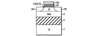
図12は上述の歪シリコン層5に形成されたMISFET(MOSFET)の断面図で
ある。このMISFETは以下のようにして形成される。まず歪Si層5の表面を熱酸化
して10nm程度の薄いゲート酸化膜101が形成される。次に閾値電圧調整用のたとえ
ばn型不純物イオンがゲート酸化膜101を介してチャネル領域に注入され、n型チャネ
ル領域が形成される。
FIG. 12 is a cross-sectional view of a MISFET (MOSFET) formed in the
次にゲート酸化膜101上にゲート電極102となるポリシリコン膜2を減圧CVD法
により形成した後、このポリシリコン膜をRIE(ReactiveIon Etchi
ng)によりパターンニングして、ゲート電極102が形成される。
Next, after the
ng) to form a
次にゲート電極102をマスクにして、リンイオンなどのn型不純物イオンを選択的に
注入した後、例えば800℃程度のアニール処理を施すことにより、n型ソース領域10
3、n型ドレイン領域104がゲート電極102に自己整合的に形成される。このように
してnチャネル型MISFETが形成されるが、不純物をp型に変更することによりpチ
ャネル型MISFETも同様にして形成できる。
Next, n-type impurity ions such as phosphorus ions are selectively implanted using the
3. An n-
上記のように形成されたMISFETは、歪Si層中に形成されているので、チャネル
領域における電子散乱が抑制され電子移動度が向上する。またMISFETは厚さ100
nm以下の薄いSOI層に形成されているので、電子移動度の向上に加えて寄生容量も低
減される。この結果駆動力に優れたMISFETを得ることができる。
Since the MISFET formed as described above is formed in the strained Si layer, electron scattering in the channel region is suppressed and the electron mobility is improved. MISFET has a thickness of 100
Since it is formed in a thin SOI layer of nm or less, parasitic capacitance is reduced in addition to the improvement of electron mobility. As a result, a MISFET excellent in driving force can be obtained.
(第2の実施形態)
図4は本発明の第2の実施例に係る半導体基板の製造方法を示す断面図である。
(Second Embodiment)
FIG. 4 is a sectional view showing a method for manufacturing a semiconductor substrate according to a second embodiment of the present invention.
本実施例においては、Si基板21上にエピタキシャルSi層6を形成後、SiGe層
4を積層し、このSiGe層4上にSi酸化膜9を形成したものが張り合わせ基板の一方
として使用される。
In the present embodiment, an
先ず、図4Aに示すように、Si基板1上に予め第1の実施例と同様にSi酸化膜2を
形成する。
First, as shown in FIG. 4A, a
次に図4Bに示すようにあらかじめ別のSi基板21上に素子形成層となるSi層6が
エピタキシャル法により形成され、このSi層6上に第1の実施例と同様にSiGe層4
が形成される。SiGe層4は基本的にはアンドープとされる。またSiGe層4は少な
くともSi層6側のGe組成が100atm%未満、Si層6とは反対側のGe組成が0
atm%より大であることが必要である。さらにSiGe層4は、高性能化のために少な
くともSi層6側、より望ましくは全体のGe組成を30atm%より大とすることが望
ましい。Ge組成を30atm%より大きくすると、歪Si層における電子移動度を高く
することができるからである。一方、SiGe層4のGe組成は80atm%以下である
ことが望ましい。
Next, as shown in FIG. 4B, a
Is formed. The
It must be greater than atm%. Furthermore, it is desirable that the
さらにこの後SiGe層4上にSi酸化膜9を形成する。
Thereafter, a
次に、図4Cに示すように、Si酸化膜2の上面2sとSi酸化膜9の上面9sと合わ
せて、2つのSi基板1及び21を実施例1と同様に張り合わせる。この結果図4Cに示
すように、Si酸化膜2とSi酸化膜9が一体化してSi酸化膜12となる。張り合わせ
後はSi基板12の剥離が行われる。
Next, as shown in FIG. 4C, the two
張り合わせ後に、水素注入によって剥離を行う場合はSi層6とSi基板21の界面も
しくは、Si層6側に水素を注入後、Si基板21が剥離される。このようにすることで
Si基板21から受けていた圧縮歪が開放されSiGe層4が格子緩和されると同時に素
子形成層となるSi層6に歪が導入される。
When peeling is performed by hydrogen injection after bonding, hydrogen is injected into the interface between the
このようにして、Si基板1と、このSi基板1上に形成されたSi酸化膜12と、こ
のSi酸化膜12上に張り合わせにより形成された格子緩和SiGe層4と、この格子緩
和SiGe層4上に形成された歪Si層6からなる半導体基板が形成される。
Thus, the
このようにして形成された歪Si層6は、CZ基板中に含まれる酸素析出や不純物が少
なく、所望の抵抗値を有する理想的な薄膜層が実現する。
The
Si酸化膜2と格子緩和SiGe層4とは実質的には直接接しているがその界面に0〜
5nmより好ましくは0〜2nmの界面バッファ層を有していてもよい。この界面バッフ
ァ層は例えばSiからなるものが挙げられる。
The
It may have an interface buffer layer of 5 nm, preferably 0-2 nm. An example of the interface buffer layer is one made of Si.
第2の実施例では、予め素子形成層となるSi層6を所望の電気特性を示すように形成
できるので再成長過程を必要としない。また、SiGe層4を形成した後に、さらにシリ
コン酸化膜9を形成し、酸化膜2と9同士を張り合わせすることによって、よりSiGe
層4に与える影響を低減できる。
In the second embodiment, since the
The influence on the
また、清浄雰囲気中にてプロセスが連続に進行する場合以外で、例えば大気中を介して
プロセスを行う場合は、SiGe層4の上に酸化膜が形成されている場合が想定され、意
図せずに図4B中のシリコン酸化膜9の形成されることもある。
In addition, when the process is performed continuously in the atmosphere other than the case where the process proceeds continuously in a clean atmosphere, for example, an oxide film is formed on the
以後、第1の実施例と同様に図12に示すMISFETが歪Si層に形成される。第2
の実施例においても駆動力に優れたMISFETを得ることができる。
Thereafter, as in the first embodiment, the MISFET shown in FIG. 12 is formed in the strained Si layer. Second
Also in this embodiment, a MISFET excellent in driving force can be obtained.
(第3の実施形態)
図5は本発明の第3の実施例に係る半導体基板の製造方法を段階的に示す半導体基板の
断面図である。
(Third embodiment)
FIG. 5 is a cross-sectional view of a semiconductor substrate showing stepwise a method of manufacturing a semiconductor substrate according to a third embodiment of the present invention.
第3の実施例は、図5Cに示すSiGe層7が膜厚方向に組成の分布を有することであ
る。即ち図6に示すようにSiGe層7中のGe濃度がSi基板1側にて低濃度、歪Si
層8側にて高濃度になるように結晶成長が行われる。これによりSiGe層7の格子間距
離を厚さ方向に不均一となる。
The third embodiment is that the
Crystal growth is performed so that the concentration is high on the
このときSi基板1側のGe組成が0%より高く、Si層8側のGe組成が100at
m%未満であることが必要である。具体的にはSi基板1側のGe濃度が0atm%より
高く30atm%以下で、歪Si層8側のGe濃度が30atm%より大きく100at
m%未満、より好ましくは80atm%以下であるようにSiGe層7中のGe組成を制
御することが望ましい。
At this time, the Ge composition on the
It is necessary to be less than m%. Specifically, the Ge concentration on the
It is desirable to control the Ge composition in the
このようにSiGe層7の組成を制御することによって、Si酸化膜2とSiGe層7
の界面から発生した転位はSiGe層7中をループが形成するように進行し、SiGe層
7と歪Si層8の界面には届かない。よってより良好な歪Si層8を提供できる。
By controlling the composition of the
Dislocations generated from the interface proceed so as to form a loop in the
以下半導体基板の製造方法を説明する。 A method for manufacturing a semiconductor substrate will be described below.
先ず、図5Aに示すように、Si基板1上に第1の実施形態と同様に予めSi酸化膜2
を形成する。
First, as shown in FIG. 5A, a
Form.
次に、図5B及び図6に示すように、Si基板21上にSiGe層7を形成する。この
ときのGe組成は、上記したようSi基板21からGe組成が徐々に少なくなるように制
御した。
Next, as shown in FIGS. 5B and 6, the
次に、Si酸化膜2の上面2sとSiGe層7の上面7sを合わせるように、2つのS
i基板と21を第1の実施例と同様に張り合わせる。
Next, two S's are formed so that the upper surface 2s of the
The i substrate and 21 are bonded together as in the first embodiment.
次に、第1の実施例と同様にSi基板21を剥離し、SiGe層7を格子緩和させる。
Next, as in the first embodiment, the
このときSi基板21の表面のSi層をごく薄く残すようにするとSiGe層4が格子
緩和されると同時に、Si層8に引っ張り歪が導入される。こうすることで転位やピット
や突起のない良好な歪Si層8を形成できる。
At this time, if the Si layer on the surface of the
このようにして、Si基板1と、このSi基板1上に形成されたSi酸化膜2と、この
Si酸化膜2上に張り合わせにより形成されGeの組成が徐々に変化した格子緩和SiG
e層7と、この格子緩和SiGe層7上に形成された歪Si層8からなる半導体基板が形
成される。
In this way, the
A semiconductor substrate including the
Si酸化膜2と格子緩和SiGe層7とは実質的には直接接しているがその界面に0〜
5nmより好ましくは0〜2nmの界面バッファ層を有していてもよい。この界面バッフ
ァ層は例えばSiからなるものが挙げられる。
The
It may have an interface buffer layer of 5 nm, preferably 0-2 nm. An example of the interface buffer layer is one made of Si.
研磨或いは剥離工程をSiGe層7までおよぼして、先ずSiGe層7を格子緩和させ
、次にMBEやCVD法によってシリコン層をごく薄く再成長させることによって歪Si
層8を形成することも可能である。
A strained Si layer is formed by extending the polishing or peeling process up to the
It is also possible to form the
また、本実施例では、SiGe層7中のGe濃度は、Si酸化膜2に近いほど低いため
、Si酸化膜2とSiGe層7の界面で発生した欠陥はSi酸化膜2側に閉じこめられて
、張り合わせ後のSiGe層7の歪Si層8との界面は格子緩和したSiGe層が得られ
る。それにより良好に緩和したSiGe層7の上に、引っ張り歪みを有する歪Si層8が
形成される。
In this embodiment, since the Ge concentration in the
また、図中の各層の厚み、アニール温度、アニール時間、張り合わせ後に剥離あるいは
研磨で残すSi基板層21の厚みなどの差異によって、緩和の程度が異なり、プロセス条
件によっては、圧縮比歪みを有するあるいは歪みの無いSiデバイス層を形成することも
可能である。
In addition, the degree of relaxation differs depending on the thickness of each layer in the figure, annealing temperature, annealing time, thickness of the
以後、第1の実施例と同様に図12に示すMISFETが歪Si層に形成される。第3
の実施例においても駆動力に優れたMISFETを得ることができる。
(第4の実施形態)
図7は本発明の第4の実施例に係る半導体基板の製造方法を示す断面図である。
Thereafter, as in the first embodiment, the MISFET shown in FIG. 12 is formed in the strained Si layer. Third
Also in this embodiment, a MISFET excellent in driving force can be obtained.
(Fourth embodiment)
FIG. 7 is a sectional view showing a method for manufacturing a semiconductor substrate according to a fourth embodiment of the present invention.
第4の実施例では、図7Bに示すSi基板21上のSiGe層7中のGe濃度が図8に
示すように膜厚方向に濃度勾配を有し、Ge濃度の最も高い部分が界面ではなくSiGe
層7の膜中に位置する。その後、Ge濃度勾配の高い部分が表面となるように剥離あるい
は薄膜化工程が施され、図7B及び図8に点線で示される面が薄膜化されたSiGe層7
の上面7sとなる。このようにSiGe層7の組成を制御した基板を用いることによって
得られた図7Cに示される半導体基板はSi酸化膜2とSiGe層7´の界面から発生し
た転位はSiGe層7中をループが形成するように進行し、SiGe層7´と歪Si層8
の界面には届かない。よってより良好な歪Si層を提供できる。
In the fourth embodiment, the Ge concentration in the
Located in the film of
The upper surface 7s. In the semiconductor substrate shown in FIG. 7C obtained by using the substrate in which the composition of the
It does not reach the interface. Therefore, a better strained Si layer can be provided.
さらに、張り合わせ前のSiGe層7の結晶成長が、Si基板21上に低Ge濃度から
開始するので、ミスマッチによる欠陥が導入され難く、良質な結晶性を有するSiGe層
7´が得られる。
Furthermore, since the crystal growth of the
以下、半導体基板の製造方法を説明する。 Hereinafter, a method for manufacturing a semiconductor substrate will be described.
先ず、図7Aに示すように、Si基板1上に予め第1の実施形態と同様にSi酸化膜2
を形成する。
First, as shown in FIG. 7A, the
Form.
次に、図7B及び図8に示すように、Si基板21上に予めSiGe層7をGe組成比
が膜方向に0atm%→35atm%→0atm%となるように形成する。続いてSiG
e7のGe組成比が最も高い中央部まで薄膜化し、SiGe層7´とする。この結果Si
Ge層7´の上面7sにはGe組成比35atm%の面が露出される。
Next, as shown in FIGS. 7B and 8, the
The film is thinned down to the central portion where the Ge composition ratio of e7 is the highest to form a
A surface having a Ge composition ratio of 35 atm% is exposed on the upper surface 7s of the Ge layer 7 '.
次に、Si酸化膜2の上面2sとSiGe7´の上面7とを合わせるように2つのSi
基板1と21を第1の実施例と同様に張り合わせる。続いて、第1の実施例と同様にSi
基板21を除去し、SiGe層7´を格子緩和させる。このときSi基板21の表面のS
i層をごく薄く残すようにするとSiGe層4が格子緩和されると同時に、Si層8に引
っ張り歪が導入される。こうすることで転位やピットや突起のない良好な歪Si層8を形
成できる。
Next, two Si are arranged so that the upper surface 2s of the
The
The
If the i layer is left extremely thin, the lattice relaxation of the
このようにして、Si基板1と、このSi基板1上に形成されたSi酸化膜2と、この
Si酸化膜2上に張り合わせにより形成されGeの組成が徐々に変化した格子緩和SiG
e層7と、この格子緩和SiGe層7´上に形成された歪Si層8からなる半導体基板が
形成される。これにより第3の実施例と同様な効果を得ることができる。
In this way, the
A semiconductor substrate including the
Si酸化膜2と格子緩和SiGe層7´とは実質的には直接接しているがその界面に0
〜5nmより好ましくは0〜2nmの界面バッファ層を有していてもよい。この界面バッ
ファ層は例えばSiからなるものが挙げられる。
The
It may have an interface buffer layer of ˜5 nm, preferably 0˜2 nm. An example of the interface buffer layer is one made of Si.
研磨或いは剥離工程をSiGe層7までおよぼして、先ずSiGe層7を格子緩和させ
、次にMBEやCVD法によってシリコン層をごく薄く再成長させることによって歪Si
層8を形成することも可能である。
A strained Si layer is formed by extending the polishing or peeling process up to the
It is also possible to form the
以後第1の実施例と同様に図12に示すMISFETが歪Si層8に形成される。第4
の実施例においても駆動力に優れたMISFETを得ることができる。
Thereafter, the MISFET shown in FIG. 12 is formed in the
Also in this embodiment, a MISFET excellent in driving force can be obtained.
(第5の実施形態)
図9は本発明の第5の実施例に係る半導体基板の製造方法を示す半導体基板の断面図で
ある。
(Fifth embodiment)
FIG. 9 is a cross-sectional view of a semiconductor substrate showing a method of manufacturing a semiconductor substrate according to a fifth embodiment of the present invention.
第5の実施例では、Si基板21上に、転位が導入される格子緩和SiGe層40と格
子緩和したSiGe層11からなるSiGe層を形成する。SiGe層40は、充分に厚
く、かつGe濃度が結晶成長と共に変化する層であって、いわゆるバッファ層としての役
割を果たす。例えば、SiGeバッファ層40はSi基板21上でのGe濃度が0atm
%であり、結晶成長と共にGe濃度が増加し、2μmの厚みにてGe濃度が30atm%
となる傾斜組成を有する構造とする。
In the fifth embodiment, a SiGe layer including a lattice-relaxed
The Ge concentration increases with crystal growth, and the Ge concentration is 30 atm% at a thickness of 2 μm.
The structure has a gradient composition.
以下半導体基板の製造方法を説明する。 A method for manufacturing a semiconductor substrate will be described below.
先ず、図9Aに示すように、Si基板1上に第1の実施例と同様に予めSi酸化膜2を
形成する。
First, as shown in FIG. 9A, a
次に、図9Bに示すように、別のSi基板21上に上記したようなGe組成のSiGe
バッファ層40を十分に厚く形成し格子緩和させる。このときSiGeバッファ層4中に
は転位33が発生するが十分に厚いのでその上に形成される半導体層に対し影響を与えな
い。次に、この格子緩和したSiGeバッファ層4上に格子緩和した結晶状態の良好なS
iGe層11を形成する。SiGeの各層の成長方法は第1の実施例に順ずる。
Next, as shown in FIG. 9B, SiGe having the Ge composition as described above is formed on another
The
The
次に、Si酸化膜2の上面2sと格子緩和したSiGe層11の上面11sを合わせる
ように第1の実施例と同様に2つのSi基板1と21を張り合わせる。
Next, the two
次に、Si基板21とSiGeバッファ層40を研磨あるいは水素注入法になどにより
除去する。次に、格子緩和したSiGe層11上に歪Si層8を形成する。(図9C)こ
のようにして、Si基板1と、このSi基板1上に形成されたSi酸化膜2と、このSi
酸化膜2上に張り合わせにより形成された格子緩和SiGe層11と、この格子緩和Si
Ge層11上に形成された歪Si層8からなる半導体基板が形成される。
Next, the
The lattice-relaxed
A semiconductor substrate made of the
SiGeバッファ層40は、SiGeバッファ層40中のSi基板21側に格子ミスマ
ッチで生じる貫通転位、ミスフィット転位などの欠陥が閉じこめられる。その結果SiG
eバッファ層40の表面側では、転位が無く格子緩和したSiGe層が実現される。
In the
On the surface side of the
このSiGeバッファ層40の表面側Ge濃度は、Siデバイス層に所望の歪みが印加
されるような濃度であって、典型的には30atm%より大きく80atm%以下であり
、膜厚方向のGe濃度分布が均一である必要はない。このSiGe層40の形成に引き続
いて、SiGeバッファ層4の表面側組成と同等の組成を有するSiGe層11を成長さ
せることで、転位などの欠陥密度を低減した高品質緩和SiGe層11が形成される。
The surface-side Ge concentration of the
ここで課題となるのはバッファ層として数μmのSiGe層40の結晶成長には原材料
と成長時間がかかりプロセスコストが要求されることにある。前述のように張り合わせ後
の薄膜化プロセスによって歪チャネル層と緩和SiGe層の積層構造が実現できる。しか
しながら張り合わせ前に所望の厚さのSiGe層が得られるように例えば0.3μm程度
の深さカット面で40c(図9B)に水素注入を行い、貼りあわせ後剥離を行うようにし
てもよい。このようにすれば剥離後に残る格子緩和SiGeバッファ層を再利用できるた
めプロセスの簡略化、半導体資源の節約が可能で、ひいては基板製造コストの低減が実現
できる。
The problem here is that the crystal growth of the
以後第1の実施例と同様に図12に示すMISFETが歪Si層8に形成される。第5
の実施例においても駆動力に優れたMISFETを得ることができる。
Thereafter, the MISFET shown in FIG. 12 is formed in the
Also in this embodiment, a MISFET excellent in driving force can be obtained.
(第6の実施形態)
図10は本発明の第6の実施例に係る半導体基板の製造方法を示す半導体基板の断面図
である。
(Sixth embodiment)
FIG. 10 is a cross-sectional view of a semiconductor substrate showing a method of manufacturing a semiconductor substrate according to a sixth embodiment of the present invention.
第6の実施例では時10Bで示すSi基板21上に、転位を導入される格子緩和SiG
eバッファ層40、格子緩和SiGeバッファ層40上に格子緩和SiGe層11、歪S
i層10、別の格子緩和SiGe層13を連続して形成後に、張り合わせプロセスを行う
。
In the sixth embodiment, lattice-relaxed SiG into which dislocations are introduced on the
e
After the
先ず、図10Aに示すように、Si基板1上に第1の実施例と同様に予めSi酸化膜2
を形成する。
First, as shown in FIG. 10A, a
Form.
次に、図10Bに示すように、別のSi基板21上に第5の実施例と同様に予めSiG
eバッファ層40を厚く形成し格子緩和させる。この格子緩和したSiGeバッファ層4
0上に、格子緩和SiGe層11、歪Si層10、格子緩和SiGe層13を続けて成長
する。
Next, as shown in FIG. 10B, SiG is previously formed on another
The
A lattice-relaxed
次に、図6(c)に示すように、Si酸化膜2の上面2sと格子緩和SiGe膜13の
上面13sをあわせるようにSi基板1と21を第1の実施例と同様に張り合わせる。
Next, as shown in FIG. 6C, the
次に、歪Si層10が表面に出るように研磨あるいは水素注入法によりSi基板21、
格子緩和SiGeバッファ層40、格子緩和SiGe層11を除去する。(図10C)こ
のようにして、Si基板1と、このSi基板1上に形成されたSi酸化膜2と、このSi
酸化膜2上に張り合わせにより形成され格子緩和SiGe層13と、この格子緩和SiG
e層13上に形成された歪Si層10からなる半導体基板が形成される。
Next, the
The lattice relaxation
A lattice-relaxed
A semiconductor substrate made of the
本実施例ではSi基板21上に形成された格子緩和SiGe層11上のSi層10は自
ずと引っ張り歪みを受けており、さらにその上のSiGe層13は緩和した層となる。
In this embodiment, the
格子緩和SiGe層13は貼り合わせ後の絶縁層2とSiGe層13からの界面から発
生する欠陥を低減するために、第3あるいは第4の実施例のように、Ge組成に勾配をつ
けてもよい。
In order to reduce defects generated from the interface between the insulating
また、格子緩和SiGe層13の上には、第2の実施例のように、予め絶縁層9を形成
してから張り合わせを行っても良い。
In addition, as in the second embodiment, the insulating
第6の実施例では、緩和率の高いSiGe層13の上に歪みの印加されたSi層10を
直接形成することが出来る上、格子緩和SiGe層13中のGe濃度を30atm%より
大きく100atm%未満の間で任意に選ぶことが可能であり、更には、絶縁層2上のS
iGe層13と歪Siデバイス層10の厚みをそれぞれ10nm以下にすることも可能で
ある。
In the sixth embodiment, the
The thicknesses of the
その結果、絶縁膜2上の合計厚みを40nm以下に抑えることが容易でありSOI効果
を十分に達成し、かつ十分な歪みをSiデバイス層10に印加できる。
As a result, the total thickness on the insulating
以後第1の実施例と同様に第6の実施例においても駆動力に優れたMISFETを得る
ことができる。
Thereafter, as in the first embodiment, the MISFET excellent in driving force can also be obtained in the sixth embodiment.
(第7の実施形態)
図11は本発明の第7の実施例に係る半導体基板の製造方法を示す半導体基板の断面図
である。
(Seventh embodiment)
FIG. 11 is a cross-sectional view of a semiconductor substrate showing a method for manufacturing a semiconductor substrate according to a seventh embodiment of the present invention.
本実施例は、貼り合わせ基板の一方としてSi基板21の替わりにSiGe基板31を
用い、SiGe基板31上に再成長した格子緩和SiGe層11と歪Si層10と格子緩
和SiGe層13とSi酸化膜9を形成した構造で説明する。
In this embodiment, a
先ず、図11Aに示すように、Si基板1上に第1の実施例と同様に予めSi酸化膜2
を形成する。
First, as shown in FIG. 11A, the
Form.
次に、図11Bに示すように、SiGe基板31上に第1の実施例と同様に予めSiG
e層11を形成し、このSiGe層11上に、Si層10、SiGe層13(Si層10
側のGe組成が30atm%より大)、Si酸化膜9を続けて成長する。
Next, as shown in FIG. 11B, a
The
The
次に、Si酸化膜2の上面2sとSi酸化膜9の上面9sを合わせるようにSi基板1
とSiGe基板31を第1の実施例と同様に張り合わせる。次に、Si層10が表面に出
るように研磨あるいは水素注入法などによりSiGe基板31、SiGe層11を除去す
る。
Next, the
And
このようにして、図11Cに示すようにSi基板1と、このSi基板1上に形成された
Si酸化膜12と、このSi酸化膜12上に張り合わせにより形成され格子緩和SiGe
層13と、この格子緩和SiGe層13上に形成された歪Si層10からなる半導体基板
が形成される。
Thus, as shown in FIG. 11C, the
A semiconductor substrate including the
この場合貼りあわせのためにはSi酸化膜2あるいはSi酸化膜9の少なくとも一方が
あればよい。また、張り合わせ工程や薄膜化工程あるいは剥離工程中にSiGe層13と
絶縁層9の接合面から発生する恐れのある欠陥を閉じこめる効果を得るには、絶縁層に接
するSiGe層13中のGe濃度を不均一にするとよい。
In this case, at least one of the
本実施例では、基板31がストレッサーとなる層11と同じSiGe組成を持つ場合を
示したが、基板上に形成する層中で組成制御を行って、所望の濃度に設定することも可能
である。
In the present embodiment, the case where the
以後第1の実施例と同様に図12に示すMISFETが歪Si層10に形成される。第
6の実施例においても、駆動力に優れたMISFETを得ることができる。
Thereafter, the MISFET shown in FIG. 12 is formed in the
また、上記第1乃至第7の実施例では、歪みを印加する層(第1の半導体層)がSiG
e層、デバイス層(第2の半導体層)がSi層の場合について説明したが、第2の半導体
層に引っ張り歪が生じるよう、第2の半導体層の格子定数が第1の半導体層の格子定数よ
りも小さくなるよう格子定数の異なる2層の組み合わせで有れば、どの様な結晶を選んで
も良く、具体的には、Si、GaAs、SiC、GaN、GaAlAs、InGaP、I
nGaPAs、Al2O3、BN、BNC、C、高濃度に不純物添加されたSi(不純物
B)、Si(不純物P)、Si(不純物As)、SiNx、ZnSeなどの物質の内、2
種類の物質の組み合わせにて、本発明の効果が得られる。但し第1の半導体層中に含有さ
れるBの濃度は1×10²⁰未満であることが望ましい。
In the first to seventh embodiments, the strain applying layer (first semiconductor layer) is SiG.
The case where the e layer and the device layer (second semiconductor layer) are Si layers has been described, but the lattice constant of the second semiconductor layer is the lattice of the first semiconductor layer so that tensile strain is generated in the second semiconductor layer. Any crystal may be selected as long as it is a combination of two layers having different lattice constants so as to be smaller than the constant, and specifically, Si, GaAs, SiC, GaN, GaAlAs, InGaP, I
Among the substances such as nGaPAs, Al 2 O 3 , BN, BNC, C, Si (impurity B), Si (impurity P), Si (impurity As), SiNx, ZnSe, and the like, which are highly doped, 2
The effect of the present invention can be obtained by combining various kinds of substances. However, the concentration of B contained in the first semiconductor layer is preferably less than 1 × 10 20 .
上記第1乃至第7の実施例では、基板1,21、31としては、Si基板、SiGe基
板を用いたが、GaAs、ZnSe、SiC、Ge、サファイア、有機ガラス、無機ガラ
ス、プラスティックのいずれかであっても良い。
In the first to seventh embodiments, Si substrates and SiGe substrates are used as the
上記第1乃至第7の実施例では絶縁膜2、9としてSi酸化膜を使用したが、シリコン
酸窒化膜、シリコン窒化膜、などの他の絶縁膜であっても良い。
In the first to seventh embodiments, Si oxide films are used as the insulating
1・・・・Si基板
2・・・・絶縁層(Si酸化膜層)
3・・・・SOI層
4・・・・SiGe層
5・・・・歪Si層
6・・・・歪エピタキシャルSi層
7・・・・傾斜組成SiGe層
8・・・・再成長で形成する歪Si層
9・・・・絶縁層
10・・・・歪Si層
11・・・・SiGe層
12・・・・絶縁層
13・・・・SiGe層
21・・・・Si基板
31・・・・SiGe基板
33・・・・転位
1 ....
3 ...
Claims (4)
第2のSi基板上に、SiGeバッファ層、第1の格子緩和SiGe層、歪Si層およ
び第2の格子緩和SiGe層の積層を順に形成する工程と、
前記第1のSi基板上に形成された絶縁膜と、前記第2のSi基板上に形成された第2
の格子緩和SiGe層と、を貼り合わせる工程と、
前記第2のSi基板、前記SiGeバッファ層、前記第1の格子緩和SiGe層を除去
して、前記第1のSi基板、前記絶縁膜、前記第2の格子緩和SiGe層および前記歪S
i層の積層を形成する工程と、
を具備することを特徴とする半導体基板の製造方法。 Forming an insulating film on the first Si substrate;
Forming a stack of an SiGe buffer layer, a first lattice relaxed SiGe layer, a strained Si layer, and a second lattice relaxed SiGe layer on the second Si substrate in order;
An insulating film formed on the first Si substrate; and a second film formed on the second Si substrate.
Bonding the lattice relaxed SiGe layer,
The second Si substrate, the SiGe buffer layer, and the first lattice relaxed SiGe layer are removed, and the first Si substrate, the insulating film, the second lattice relaxed SiGe layer, and the strain S are removed.
forming a stack of i layers;
A method for manufacturing a semiconductor substrate, comprising:
ざかるに従ってGe濃度が徐々に高くなることを特徴とする請求項1に記載の半導体装置
の製造方法。 The method of manufacturing a semiconductor device according to claim 1, wherein the SiGe buffer layer has a Ge concentration gradient in a film thickness direction, and the Ge concentration gradually increases as the distance from the second Si substrate side increases.
SiGe基板上に、第1の格子緩和SiGe層、歪Si層、第2の格子緩和SiGe層
および第2の絶縁膜を順次形成する工程と、
前記Si基板上に形成された第1の絶縁膜と、前記SiGe基板上に形成された第2の
絶縁膜と、を貼り合わせる工程と、
前記SiGe基板および前記第1の格子緩和SiGe層を除去して、前記Si基板、前
記第1および第2の絶縁膜、前記第2の格子緩和SiGe層ならびに前記歪Si層の積層
を形成する工程と、
を具備することを特徴とする半導体基板の製造方法。 Forming a first insulating film on the Si substrate;
Forming a first lattice-relaxed SiGe layer, a strained Si layer, a second lattice-relaxed SiGe layer, and a second insulating film on the SiGe substrate sequentially;
Bonding the first insulating film formed on the Si substrate and the second insulating film formed on the SiGe substrate;
Removing the SiGe substrate and the first lattice relaxed SiGe layer to form a stack of the Si substrate, the first and second insulating films, the second lattice relaxed SiGe layer, and the strained Si layer; When,
A method for manufacturing a semiconductor substrate, comprising:
第2のSi基板上に、SiGeバッファ層と、前記SiGeバッファ層上に形成された
格子緩和SiGe層とを形成する工程と、
前記第1のSi基板上に形成された絶縁膜と、前記第2のSi基板上に形成された格子
緩和SiGe層と、を貼り合わせる工程と、
前記第2のSi基板、前記SiGeバッファ層を除去して、前記第1のSi基板、前記
絶縁膜及び前記格子緩和SiGe層、の積層を形成する工程と、
前記格子緩和SiGe層上に、引っ張り格子歪が印加されたSi層を形成する工程と、
を具備することを特徴とする半導体基板の製造方法。 Forming an insulating film on the first Si substrate;
Forming a SiGe buffer layer and a lattice relaxation SiGe layer formed on the SiGe buffer layer on a second Si substrate;
Bonding the insulating film formed on the first Si substrate and the lattice relaxed SiGe layer formed on the second Si substrate;
Removing the second Si substrate and the SiGe buffer layer to form a stack of the first Si substrate, the insulating film and the lattice-relaxed SiGe layer;
Forming a Si layer to which a tensile lattice strain is applied on the lattice-relaxed SiGe layer;
A method for manufacturing a semiconductor substrate, comprising:
Priority Applications (1)
| Application Number | Priority Date | Filing Date | Title |
|---|---|---|---|
| JP2008325864A JP2009105427A (en) | 1999-11-26 | 2008-12-22 | Manufacturing method of semiconductor substrate |
Applications Claiming Priority (2)
| Application Number | Priority Date | Filing Date | Title |
|---|---|---|---|
| JP33605999 | 1999-11-26 | ||
| JP2008325864A JP2009105427A (en) | 1999-11-26 | 2008-12-22 | Manufacturing method of semiconductor substrate |
Related Parent Applications (1)
| Application Number | Title | Priority Date | Filing Date |
|---|---|---|---|
| JP2004215495A Division JP4282560B2 (en) | 1999-11-26 | 2004-07-23 | Manufacturing method of semiconductor substrate |
Publications (1)
| Publication Number | Publication Date |
|---|---|
| JP2009105427A true JP2009105427A (en) | 2009-05-14 |
Family
ID=30767607
Family Applications (1)
| Application Number | Title | Priority Date | Filing Date |
|---|---|---|---|
| JP2008325864A Abandoned JP2009105427A (en) | 1999-11-26 | 2008-12-22 | Manufacturing method of semiconductor substrate |
Country Status (2)
| Country | Link |
|---|---|
| US (2) | US6690043B1 (en) |
| JP (1) | JP2009105427A (en) |
Cited By (1)
| Publication number | Priority date | Publication date | Assignee | Title |
|---|---|---|---|---|
| JP2018060959A (en) * | 2016-10-07 | 2018-04-12 | 株式会社Sumco | Epitaxial silicon wafer and method of manufacturing epitaxial silicon wafer |
Families Citing this family (65)
| Publication number | Priority date | Publication date | Assignee | Title |
|---|---|---|---|---|
| US7227176B2 (en) | 1998-04-10 | 2007-06-05 | Massachusetts Institute Of Technology | Etch stop layer system |
| JP4207548B2 (en) * | 2002-11-28 | 2009-01-14 | 株式会社Sumco | Semiconductor substrate manufacturing method, field effect transistor manufacturing method, semiconductor substrate, and field effect transistor |
| EP1309989B1 (en) * | 2000-08-16 | 2007-01-10 | Massachusetts Institute Of Technology | Process for producing semiconductor article using graded expitaxial growth |
| US6649480B2 (en) * | 2000-12-04 | 2003-11-18 | Amberwave Systems Corporation | Method of fabricating CMOS inverter and integrated circuits utilizing strained silicon surface channel MOSFETs |
| US6830976B2 (en) * | 2001-03-02 | 2004-12-14 | Amberwave Systems Corproation | Relaxed silicon germanium platform for high speed CMOS electronics and high speed analog circuits |
| US6703688B1 (en) * | 2001-03-02 | 2004-03-09 | Amberwave Systems Corporation | Relaxed silicon germanium platform for high speed CMOS electronics and high speed analog circuits |
| WO2002082514A1 (en) * | 2001-04-04 | 2002-10-17 | Massachusetts Institute Of Technology | A method for semiconductor device fabrication |
| WO2003017336A2 (en) * | 2001-08-13 | 2003-02-27 | Amberwave Systems Corporation | Dram trench capacitor and method of making the same |
| US20030230778A1 (en) * | 2002-01-30 | 2003-12-18 | Sumitomo Mitsubishi Silicon Corporation | SOI structure having a SiGe Layer interposed between the silicon and the insulator |
| JP2003249641A (en) * | 2002-02-22 | 2003-09-05 | Sharp Corp | Semiconductor substrate, method of manufacturing the same, and semiconductor device |
| AU2003222003A1 (en) * | 2002-03-14 | 2003-09-29 | Amberwave Systems Corporation | Methods for fabricating strained layers on semiconductor substrates |
| US6995430B2 (en) * | 2002-06-07 | 2006-02-07 | Amberwave Systems Corporation | Strained-semiconductor-on-insulator device structures |
| US7074623B2 (en) * | 2002-06-07 | 2006-07-11 | Amberwave Systems Corporation | Methods of forming strained-semiconductor-on-insulator finFET device structures |
| US7335545B2 (en) * | 2002-06-07 | 2008-02-26 | Amberwave Systems Corporation | Control of strain in device layers by prevention of relaxation |
| US7307273B2 (en) * | 2002-06-07 | 2007-12-11 | Amberwave Systems Corporation | Control of strain in device layers by selective relaxation |
| US20030227057A1 (en) * | 2002-06-07 | 2003-12-11 | Lochtefeld Anthony J. | Strained-semiconductor-on-insulator device structures |
| JP2004014856A (en) * | 2002-06-07 | 2004-01-15 | Sharp Corp | Method for manufacturing semiconductor substrate and method for manufacturing semiconductor device |
| US6946371B2 (en) * | 2002-06-10 | 2005-09-20 | Amberwave Systems Corporation | Methods of fabricating semiconductor structures having epitaxially grown source and drain elements |
| US6982474B2 (en) * | 2002-06-25 | 2006-01-03 | Amberwave Systems Corporation | Reacted conductive gate electrodes |
| US6953736B2 (en) * | 2002-07-09 | 2005-10-11 | S.O.I.Tec Silicon On Insulator Technologies S.A. | Process for transferring a layer of strained semiconductor material |
| US6936869B2 (en) * | 2002-07-09 | 2005-08-30 | International Rectifier Corporation | Heterojunction field effect transistors using silicon-germanium and silicon-carbon alloys |
| US6841457B2 (en) * | 2002-07-16 | 2005-01-11 | International Business Machines Corporation | Use of hydrogen implantation to improve material properties of silicon-germanium-on-insulator material made by thermal diffusion |
| AU2003280307A1 (en) * | 2002-11-05 | 2004-06-07 | M 2 Medical A/S | A disposable wearable insulin dispensing device, a combination of such a device and a programming controller and a method of controlling the operation of such a device |
| US6787423B1 (en) * | 2002-12-09 | 2004-09-07 | Advanced Micro Devices, Inc. | Strained-silicon semiconductor device |
| US20090325362A1 (en) * | 2003-01-07 | 2009-12-31 | Nabil Chhaimi | Method of recycling an epitaxied donor wafer |
| ATE426918T1 (en) * | 2003-01-07 | 2009-04-15 | Soitec Silicon On Insulator | RECYCLING A WAFER WITH A MULTI-LAYER STRUCTURE AFTER REMOVING A THIN LAYER |
| WO2004061943A1 (en) * | 2003-01-07 | 2004-07-22 | S.O.I.Tec Silicon On Insulator Technologies | Recycling by mechanical means of a wafer comprising a taking-off structure after taking-off a thin layer thereof |
| US6924181B2 (en) * | 2003-02-13 | 2005-08-02 | Taiwan Semiconductor Manufacturing Co., Ltd | Strained silicon layer semiconductor product employing strained insulator layer |
| US6911379B2 (en) * | 2003-03-05 | 2005-06-28 | Taiwan Semiconductor Manufacturing Company, Ltd. | Method of forming strained silicon on insulator substrate |
| US6960781B2 (en) | 2003-03-07 | 2005-11-01 | Amberwave Systems Corporation | Shallow trench isolation process |
| US6949451B2 (en) * | 2003-03-10 | 2005-09-27 | Taiwan Semiconductor Manufacturing Company, Ltd. | SOI chip with recess-resistant buried insulator and method of manufacturing the same |
| US6902962B2 (en) * | 2003-04-04 | 2005-06-07 | Taiwan Semiconductor Manufacturing Company, Ltd. | Silicon-on-insulator chip with multiple crystal orientations |
| DE10318283A1 (en) * | 2003-04-22 | 2004-11-25 | Forschungszentrum Jülich GmbH | Process for producing a strained layer on a substrate and layer structure |
| US7354815B2 (en) * | 2003-11-18 | 2008-04-08 | Silicon Genesis Corporation | Method for fabricating semiconductor devices using strained silicon bearing material |
| JP2005244020A (en) * | 2004-02-27 | 2005-09-08 | Toshiba Corp | Semiconductor device and manufacturing method thereof |
| US7023018B2 (en) * | 2004-04-06 | 2006-04-04 | Texas Instruments Incorporated | SiGe transistor with strained layers |
| US7504693B2 (en) * | 2004-04-23 | 2009-03-17 | International Business Machines Corporation | Dislocation free stressed channels in bulk silicon and SOI CMOS devices by gate stress engineering |
| US7202145B2 (en) * | 2004-06-03 | 2007-04-10 | Taiwan Semiconductor Manufacturing Company | Strained Si formed by anneal |
| US7009226B1 (en) * | 2004-07-12 | 2006-03-07 | Advanced Micro Devices, Inc. | In-situ nitride/oxynitride processing with reduced deposition surface pattern sensitivity |
| JP4617820B2 (en) * | 2004-10-20 | 2011-01-26 | 信越半導体株式会社 | Manufacturing method of semiconductor wafer |
| US7238589B2 (en) * | 2004-11-01 | 2007-07-03 | International Business Machines Corporation | In-place bonding of microstructures |
| JP2006140187A (en) * | 2004-11-10 | 2006-06-01 | Shin Etsu Handotai Co Ltd | Manufacturing method of semiconductor wafer |
| US7393733B2 (en) | 2004-12-01 | 2008-07-01 | Amberwave Systems Corporation | Methods of forming hybrid fin field-effect transistor structures |
| US20060113603A1 (en) * | 2004-12-01 | 2006-06-01 | Amberwave Systems Corporation | Hybrid semiconductor-on-insulator structures and related methods |
| US7229901B2 (en) * | 2004-12-16 | 2007-06-12 | Wisconsin Alumni Research Foundation | Fabrication of strained heterojunction structures |
| KR100636672B1 (en) | 2004-12-22 | 2006-10-23 | 주식회사 하이닉스반도체 | Method of manufacturing transistor in semiconductor device |
| US20060151787A1 (en) * | 2005-01-12 | 2006-07-13 | International Business Machines Corporation | LOW CONCENTRATION SiGe BUFFER DURING STRAINED Si GROWTH OF SSGOI MATERIAL FOR DOPANT DIFFUSION CONTROL AND DEFECT REDUCTION |
| US8007675B1 (en) * | 2005-07-11 | 2011-08-30 | National Semiconductor Corporation | System and method for controlling an etch process for a single crystal having a buried layer |
| JP2007194336A (en) * | 2006-01-18 | 2007-08-02 | Sumco Corp | Manufacturing method of semiconductor wafer |
| US7494856B2 (en) * | 2006-03-30 | 2009-02-24 | Freescale Semiconductor, Inc. | Semiconductor fabrication process using etch stop layer to optimize formation of source/drain stressor |
| US7572712B2 (en) | 2006-11-21 | 2009-08-11 | Chartered Semiconductor Manufacturing, Ltd. | Method to form selective strained Si using lateral epitaxy |
| US20080173895A1 (en) * | 2007-01-24 | 2008-07-24 | Sharp Laboratories Of America, Inc. | Gallium nitride on silicon with a thermal expansion transition buffer layer |
| JP5152827B2 (en) * | 2007-03-22 | 2013-02-27 | 株式会社日立製作所 | THIN FILM TRANSISTOR AND ORGANIC EL DISPLAY DEVICE USING THE SAME |
| FR2917232B1 (en) * | 2007-06-06 | 2009-10-09 | Soitec Silicon On Insulator | PROCESS FOR MANUFACTURING A STRUCTURE FOR EPITAXY WITHOUT EXCLUSION AREA |
| JP5466410B2 (en) * | 2008-02-14 | 2014-04-09 | 信越化学工業株式会社 | SOI substrate surface treatment method |
| FR2929758B1 (en) * | 2008-04-07 | 2011-02-11 | Commissariat Energie Atomique | TRANSFER METHOD USING A FERROELECTRIC SUBSTRATE |
| US8232186B2 (en) * | 2008-05-29 | 2012-07-31 | International Business Machines Corporation | Methods of integrating reverse eSiGe on NFET and SiGe channel on PFET, and related structure |
| US20100109044A1 (en) * | 2008-10-30 | 2010-05-06 | Tekleab Daniel G | Optimized Compressive SiGe Channel PMOS Transistor with Engineered Ge Profile and Optimized Silicon Cap Layer |
| US7759205B1 (en) * | 2009-01-16 | 2010-07-20 | Advanced Micro Devices, Inc. | Methods for fabricating semiconductor devices minimizing under-oxide regrowth |
| US8008138B2 (en) * | 2009-11-30 | 2011-08-30 | International Business Machines Corporation | Extremely thin semiconductor on insulator semiconductor device with suppressed dopant segregation |
| US10833194B2 (en) * | 2010-08-27 | 2020-11-10 | Acorn Semi, Llc | SOI wafers and devices with buried stressor |
| DE102010046215B4 (en) * | 2010-09-21 | 2019-01-03 | Infineon Technologies Austria Ag | Semiconductor body with strained region, electronic component and a method for producing the semiconductor body. |
| US8643061B2 (en) * | 2010-10-20 | 2014-02-04 | International Business Machines Corporation | Structure of high-K metal gate semiconductor transistor |
| US8426920B2 (en) * | 2011-06-29 | 2013-04-23 | Institute of Microelectronics, Chinese Academy of Sciences | MOSFET and method for manufacturing the same |
| US8883598B2 (en) * | 2012-03-05 | 2014-11-11 | Taiwan Semiconductor Manufacturing Co., Ltd. | Thin capped channel layers of semiconductor devices and methods of forming the same |
Family Cites Families (8)
| Publication number | Priority date | Publication date | Assignee | Title |
|---|---|---|---|---|
| JP3061406B2 (en) | 1990-09-28 | 2000-07-10 | 株式会社東芝 | Semiconductor device |
| US5218213A (en) * | 1991-02-22 | 1993-06-08 | Harris Corporation | SOI wafer with sige |
| US5461243A (en) * | 1993-10-29 | 1995-10-24 | International Business Machines Corporation | Substrate for tensilely strained semiconductor |
| JP2980497B2 (en) * | 1993-11-15 | 1999-11-22 | 株式会社東芝 | Method of manufacturing dielectric-isolated bipolar transistor |
| JP3376211B2 (en) | 1996-05-29 | 2003-02-10 | 株式会社東芝 | Semiconductor device, method of manufacturing semiconductor substrate, and method of manufacturing semiconductor device |
| US5847419A (en) * | 1996-09-17 | 1998-12-08 | Kabushiki Kaisha Toshiba | Si-SiGe semiconductor device and method of fabricating the same |
| US5882987A (en) | 1997-08-26 | 1999-03-16 | International Business Machines Corporation | Smart-cut process for the production of thin semiconductor material films |
| CA2327421A1 (en) * | 1998-04-10 | 1999-10-21 | Jeffrey T. Borenstein | Silicon-germanium etch stop layer system |
-
2000
- 2000-11-22 US US09/717,039 patent/US6690043B1/en not_active Expired - Fee Related
-
2003
- 2003-12-17 US US10/736,593 patent/US7033913B2/en not_active Expired - Fee Related
-
2008
- 2008-12-22 JP JP2008325864A patent/JP2009105427A/en not_active Abandoned
Cited By (2)
| Publication number | Priority date | Publication date | Assignee | Title |
|---|---|---|---|---|
| JP2018060959A (en) * | 2016-10-07 | 2018-04-12 | 株式会社Sumco | Epitaxial silicon wafer and method of manufacturing epitaxial silicon wafer |
| US11888036B2 (en) | 2016-10-07 | 2024-01-30 | Sumco Corporation | Method for setting a nitrogen concentration of a silicon epitaxial film in manufacturing an epitaxial silicon wafer |
Also Published As
| Publication number | Publication date |
|---|---|
| US20040126958A1 (en) | 2004-07-01 |
| US6690043B1 (en) | 2004-02-10 |
| US7033913B2 (en) | 2006-04-25 |
Similar Documents
| Publication | Publication Date | Title |
|---|---|---|
| JP2009105427A (en) | Manufacturing method of semiconductor substrate | |
| JP3607194B2 (en) | Semiconductor device, semiconductor device manufacturing method, and semiconductor substrate | |
| US9548236B2 (en) | Methods of forming strained-semiconductor-on-insulator device structures | |
| US6893936B1 (en) | Method of Forming strained SI/SIGE on insulator with silicon germanium buffer | |
| KR101133871B1 (en) | Method for producing dislocation-free strained crystalline films | |
| US6603156B2 (en) | Strained silicon on insulator structures | |
| JP3512701B2 (en) | Semiconductor device and manufacturing method thereof | |
| US7482190B2 (en) | Micromechanical strained semiconductor by wafer bonding | |
| US6955952B2 (en) | Strain balanced structure with a tensile strained silicon channel and a compressive strained silicon-germanium channel for CMOS performance enhancement | |
| US20040235264A1 (en) | Gettering of silicon on insulator using relaxed silicon germanium epitaxial proximity layers | |
| JP2007533119A (en) | Silicon devices on Si: C-OI and SGOI and manufacturing methods | |
| US7416965B2 (en) | Method for producing a strained layer on a substrate and corresponding layer structure | |
| US20090085115A1 (en) | Transistor and in-situ fabrication process | |
| US7462525B2 (en) | Enhancement of electron and hole mobilities in <110> Si under biaxial compressive strain | |
| WO2005122272A1 (en) | Mis field-effect transistor having strained silicon channel layer | |
| US20030077882A1 (en) | Method of forming strained-silicon wafer for mobility-enhanced MOSFET device | |
| JP4296726B2 (en) | Manufacturing method of semiconductor substrate and manufacturing method of field effect transistor | |
| TW200539425A (en) | Integrated circuit with strained and non-strained transistors, and method of forming thereof | |
| JP4282560B2 (en) | Manufacturing method of semiconductor substrate | |
| US20050032340A1 (en) | Semiconductor device and method of manufacturing the same | |
| US7109096B2 (en) | Semiconductor device and method of manufacturing the same | |
| US20050070070A1 (en) | Method of forming strained silicon on insulator | |
| JP4037803B2 (en) | Method for manufacturing SGOI substrate | |
| JP2003008022A (en) | Semiconductor substrate, field-effect transistor, and manufacturing method thereof | |
| JP2003017670A (en) | Semiconductor substrate, field-effect transistor, and manufacturing method thereof |
Legal Events
| Date | Code | Title | Description |
|---|---|---|---|
| A762 | Written abandonment of application |
Free format text: JAPANESE INTERMEDIATE CODE: A762 Effective date: 20100121 |