JP2009038142A - Semiconductor stacked package - Google Patents
Semiconductor stacked package Download PDFInfo
- Publication number
- JP2009038142A JP2009038142A JP2007199695A JP2007199695A JP2009038142A JP 2009038142 A JP2009038142 A JP 2009038142A JP 2007199695 A JP2007199695 A JP 2007199695A JP 2007199695 A JP2007199695 A JP 2007199695A JP 2009038142 A JP2009038142 A JP 2009038142A
- Authority
- JP
- Japan
- Prior art keywords
- wiring
- semiconductor chip
- pad
- semiconductor
- wiring board
- Prior art date
- Legal status (The legal status is an assumption and is not a legal conclusion. Google has not performed a legal analysis and makes no representation as to the accuracy of the status listed.)
- Pending
Links
Images


Classifications
-
- H—ELECTRICITY
- H10—SEMICONDUCTOR DEVICES; ELECTRIC SOLID-STATE DEVICES NOT OTHERWISE PROVIDED FOR
- H10W—GENERIC PACKAGES, INTERCONNECTIONS, CONNECTORS OR OTHER CONSTRUCTIONAL DETAILS OF DEVICES COVERED BY CLASS H10
- H10W90/00—Package configurations
-
- H—ELECTRICITY
- H10—SEMICONDUCTOR DEVICES; ELECTRIC SOLID-STATE DEVICES NOT OTHERWISE PROVIDED FOR
- H10W—GENERIC PACKAGES, INTERCONNECTIONS, CONNECTORS OR OTHER CONSTRUCTIONAL DETAILS OF DEVICES COVERED BY CLASS H10
- H10W72/00—Interconnections or connectors in packages
- H10W72/01—Manufacture or treatment
-
- H—ELECTRICITY
- H10—SEMICONDUCTOR DEVICES; ELECTRIC SOLID-STATE DEVICES NOT OTHERWISE PROVIDED FOR
- H10W—GENERIC PACKAGES, INTERCONNECTIONS, CONNECTORS OR OTHER CONSTRUCTIONAL DETAILS OF DEVICES COVERED BY CLASS H10
- H10W72/00—Interconnections or connectors in packages
- H10W72/071—Connecting or disconnecting
- H10W72/075—Connecting or disconnecting of bond wires
-
- H—ELECTRICITY
- H10—SEMICONDUCTOR DEVICES; ELECTRIC SOLID-STATE DEVICES NOT OTHERWISE PROVIDED FOR
- H10W—GENERIC PACKAGES, INTERCONNECTIONS, CONNECTORS OR OTHER CONSTRUCTIONAL DETAILS OF DEVICES COVERED BY CLASS H10
- H10W72/00—Interconnections or connectors in packages
- H10W72/20—Bump connectors, e.g. solder bumps or copper pillars; Dummy bumps; Thermal bumps
- H10W72/29—Bond pads specially adapted therefor
-
- H—ELECTRICITY
- H10—SEMICONDUCTOR DEVICES; ELECTRIC SOLID-STATE DEVICES NOT OTHERWISE PROVIDED FOR
- H10W—GENERIC PACKAGES, INTERCONNECTIONS, CONNECTORS OR OTHER CONSTRUCTIONAL DETAILS OF DEVICES COVERED BY CLASS H10
- H10W72/00—Interconnections or connectors in packages
- H10W72/50—Bond wires
- H10W72/541—Dispositions of bond wires
- H10W72/547—Dispositions of multiple bond wires
- H10W72/5473—Dispositions of multiple bond wires multiple bond wires connected to a common bond pad
-
- H—ELECTRICITY
- H10—SEMICONDUCTOR DEVICES; ELECTRIC SOLID-STATE DEVICES NOT OTHERWISE PROVIDED FOR
- H10W—GENERIC PACKAGES, INTERCONNECTIONS, CONNECTORS OR OTHER CONSTRUCTIONAL DETAILS OF DEVICES COVERED BY CLASS H10
- H10W72/00—Interconnections or connectors in packages
- H10W72/50—Bond wires
- H10W72/551—Materials of bond wires
- H10W72/552—Materials of bond wires comprising metals or metalloids, e.g. silver
- H10W72/5522—Materials of bond wires comprising metals or metalloids, e.g. silver comprising gold [Au]
-
- H—ELECTRICITY
- H10—SEMICONDUCTOR DEVICES; ELECTRIC SOLID-STATE DEVICES NOT OTHERWISE PROVIDED FOR
- H10W—GENERIC PACKAGES, INTERCONNECTIONS, CONNECTORS OR OTHER CONSTRUCTIONAL DETAILS OF DEVICES COVERED BY CLASS H10
- H10W72/00—Interconnections or connectors in packages
- H10W72/50—Bond wires
- H10W72/59—Bond pads specially adapted therefor
-
- H—ELECTRICITY
- H10—SEMICONDUCTOR DEVICES; ELECTRIC SOLID-STATE DEVICES NOT OTHERWISE PROVIDED FOR
- H10W—GENERIC PACKAGES, INTERCONNECTIONS, CONNECTORS OR OTHER CONSTRUCTIONAL DETAILS OF DEVICES COVERED BY CLASS H10
- H10W72/00—Interconnections or connectors in packages
- H10W72/90—Bond pads, in general
- H10W72/931—Shapes of bond pads
- H10W72/932—Plan-view shape, i.e. in top view
-
- H—ELECTRICITY
- H10—SEMICONDUCTOR DEVICES; ELECTRIC SOLID-STATE DEVICES NOT OTHERWISE PROVIDED FOR
- H10W—GENERIC PACKAGES, INTERCONNECTIONS, CONNECTORS OR OTHER CONSTRUCTIONAL DETAILS OF DEVICES COVERED BY CLASS H10
- H10W72/00—Interconnections or connectors in packages
- H10W72/90—Bond pads, in general
- H10W72/941—Dispositions of bond pads
- H10W72/944—Dispositions of multiple bond pads
- H10W72/9445—Top-view layouts, e.g. mirror arrays
-
- H—ELECTRICITY
- H10—SEMICONDUCTOR DEVICES; ELECTRIC SOLID-STATE DEVICES NOT OTHERWISE PROVIDED FOR
- H10W—GENERIC PACKAGES, INTERCONNECTIONS, CONNECTORS OR OTHER CONSTRUCTIONAL DETAILS OF DEVICES COVERED BY CLASS H10
- H10W72/00—Interconnections or connectors in packages
- H10W72/90—Bond pads, in general
- H10W72/951—Materials of bond pads
-
- H—ELECTRICITY
- H10—SEMICONDUCTOR DEVICES; ELECTRIC SOLID-STATE DEVICES NOT OTHERWISE PROVIDED FOR
- H10W—GENERIC PACKAGES, INTERCONNECTIONS, CONNECTORS OR OTHER CONSTRUCTIONAL DETAILS OF DEVICES COVERED BY CLASS H10
- H10W74/00—Encapsulations, e.g. protective coatings
-
- H—ELECTRICITY
- H10—SEMICONDUCTOR DEVICES; ELECTRIC SOLID-STATE DEVICES NOT OTHERWISE PROVIDED FOR
- H10W—GENERIC PACKAGES, INTERCONNECTIONS, CONNECTORS OR OTHER CONSTRUCTIONAL DETAILS OF DEVICES COVERED BY CLASS H10
- H10W74/00—Encapsulations, e.g. protective coatings
- H10W74/10—Encapsulations, e.g. protective coatings characterised by their shape or disposition
- H10W74/111—Encapsulations, e.g. protective coatings characterised by their shape or disposition the semiconductor body being completely enclosed
- H10W74/114—Encapsulations, e.g. protective coatings characterised by their shape or disposition the semiconductor body being completely enclosed by a substrate and the encapsulations
- H10W74/117—Encapsulations, e.g. protective coatings characterised by their shape or disposition the semiconductor body being completely enclosed by a substrate and the encapsulations the substrate having spherical bumps for external connection
-
- H—ELECTRICITY
- H10—SEMICONDUCTOR DEVICES; ELECTRIC SOLID-STATE DEVICES NOT OTHERWISE PROVIDED FOR
- H10W—GENERIC PACKAGES, INTERCONNECTIONS, CONNECTORS OR OTHER CONSTRUCTIONAL DETAILS OF DEVICES COVERED BY CLASS H10
- H10W90/00—Package configurations
- H10W90/701—Package configurations characterised by the relative positions of pads or connectors relative to package parts
- H10W90/721—Package configurations characterised by the relative positions of pads or connectors relative to package parts of bump connectors
- H10W90/724—Package configurations characterised by the relative positions of pads or connectors relative to package parts of bump connectors between a chip and a stacked insulating package substrate, interposer or RDL
-
- H—ELECTRICITY
- H10—SEMICONDUCTOR DEVICES; ELECTRIC SOLID-STATE DEVICES NOT OTHERWISE PROVIDED FOR
- H10W—GENERIC PACKAGES, INTERCONNECTIONS, CONNECTORS OR OTHER CONSTRUCTIONAL DETAILS OF DEVICES COVERED BY CLASS H10
- H10W90/00—Package configurations
- H10W90/701—Package configurations characterised by the relative positions of pads or connectors relative to package parts
- H10W90/731—Package configurations characterised by the relative positions of pads or connectors relative to package parts of die-attach connectors
- H10W90/732—Package configurations characterised by the relative positions of pads or connectors relative to package parts of die-attach connectors between stacked chips
-
- H—ELECTRICITY
- H10—SEMICONDUCTOR DEVICES; ELECTRIC SOLID-STATE DEVICES NOT OTHERWISE PROVIDED FOR
- H10W—GENERIC PACKAGES, INTERCONNECTIONS, CONNECTORS OR OTHER CONSTRUCTIONAL DETAILS OF DEVICES COVERED BY CLASS H10
- H10W90/00—Package configurations
- H10W90/701—Package configurations characterised by the relative positions of pads or connectors relative to package parts
- H10W90/751—Package configurations characterised by the relative positions of pads or connectors relative to package parts of bond wires
- H10W90/754—Package configurations characterised by the relative positions of pads or connectors relative to package parts of bond wires between a chip and a stacked insulating package substrate, interposer or RDL
Landscapes
- Wire Bonding (AREA)
- Production Of Multi-Layered Print Wiring Board (AREA)
Abstract
【課題】本発明は、インピーダンスを小さくすることができ、ノイズや電圧降下の原因を取り除いて低ノイズで高速動作を可能とした半導体積層パッケージの提供を目的とする。
【解決手段】本発明は、第1のプリント配線板の上に複数の半導体チップが積層され、上段の半導体チップが電源系のパッドとグランド系のパッドと信号系のパッドを上面側中央部に備えた構成であり、中央に配線用孔部を有する配線拡張部が前記上段の半導体チップ上に積層され、該配線拡張部にはその中央部側からその周辺部側にかけて延出形成された配線回路が設けられ、前記上段の半導体チップの電源系のパッドとグランド系のパッドが前記配線拡張部の中央部側の配線回路に前記配線用孔部を介して接続され、前記配線拡張部の周辺部側の配線回路がワイヤー線を介して前記第1のプリント配線板上の接続ランドにボンディング接続されてなる。
【選択図】図1
An object of the present invention is to provide a semiconductor stacked package capable of reducing impedance, eliminating the cause of noise and voltage drop, and enabling high-speed operation with low noise.
A plurality of semiconductor chips are stacked on a first printed wiring board, and an upper semiconductor chip includes a power supply pad, a ground pad, and a signal pad in the center on the upper surface side. A wiring extension portion having a wiring hole portion in the center is stacked on the upper semiconductor chip, and the wiring extension portion is formed to extend from the central portion side to the peripheral portion side of the wiring extension portion. A circuit is provided, and a power supply system pad and a ground system pad of the upper semiconductor chip are connected to a wiring circuit on a central side of the wiring extension part via the wiring hole, and the periphery of the wiring extension part The wiring circuit on the part side is bonded to a connection land on the first printed wiring board via a wire.
[Selection] Figure 1
Description
本発明は低ノイズで高速動作が可能な半導体積層パッケージに関する。 The present invention relates to a semiconductor stacked package capable of high-speed operation with low noise.
従来の半導体積層パッケージの構造として、半導体チップを積層する構造や半導体パッケージを積層する構造が知られている。半導体装置の近年の高密度実装化により、更なる小型・薄型化が要求されてきており、半導体チップを積層する構造が各社から提案されている。
半導体積層チップの第1の構造例として、2つの半導体チップの裏面どうしを対向させて積層した積層構造であり、この積層構造の上面側と下面側に個々にリードフレームを備えて個々の半導体チップの回路とこれらのリードフレームをボンディング接続し、上下のリードフレームを1つのリードから分岐してなる半導体チップ積層構造が知られている。(特許文献1参照)
半導体積層チップの第2の構造例として、半導体チップを背中合わせとして一体化し、封止材の内部に設けた構造であり、封止材の内部にこれらの半導体チップと離間してプリント基板層を別途配置し、このプリント基板層を外部リードに接続し、プリント基板層と半導体チップのボンディングパッドをボンディング線で接続し、GNDライン、電源ラインを強化した構造の積層パッケージが知られている。(特許文献2参照)
半導体積層チップの第3の構造例として、上下両面にフレキシブル回路を積層した構造のパドルを介して第1半導体チップと第2半導体チップを積層し、これらチップの端子をフレキシブル回路に接続し、チップ端子を長いワイヤーを用いて外部リードに接続してなる構造の半導体チップ積層構造が知られている。(特許文献3参照)
更に、プリント配線板の上に上下2段に積層した半導体チップ構造として、下段の半導体チップの回路面を下向き(プリント配線板側)、上段の半導体チップは上向きにして積層し、下段の半導体チップのパッドからプリント配線板の下面(半導体チップ積層面の逆面)へワイヤーにて接続し、プリント配線板に接続した構造が知られている。(特許文献4参照)
As a structure of a conventional semiconductor stacked package, a structure in which semiconductor chips are stacked and a structure in which semiconductor packages are stacked are known. With recent high-density mounting of semiconductor devices, further downsizing and thinning have been required, and structures for stacking semiconductor chips have been proposed by various companies.
As a first structure example of a semiconductor multilayer chip, there is a multilayer structure in which the back surfaces of two semiconductor chips are stacked to face each other, and individual semiconductor chips each having a lead frame on the upper surface side and the lower surface side of the multilayer structure. A semiconductor chip laminated structure is known in which these circuits and these lead frames are connected by bonding, and upper and lower lead frames are branched from one lead. (See Patent Document 1)
As a second structure example of the semiconductor multilayer chip, the semiconductor chips are integrated as a back-to-back structure and provided inside the encapsulant, and a printed circuit board layer is separately provided inside the encapsulant so as to be separated from these semiconductor chips. A stacked package having a structure in which the printed circuit board layer is connected to an external lead, the printed circuit board layer and a bonding pad of a semiconductor chip are connected by a bonding line, and a GND line and a power supply line are reinforced is known. (See Patent Document 2)
As a third structural example of the semiconductor laminated chip, the first semiconductor chip and the second semiconductor chip are laminated through paddles having a structure in which flexible circuits are laminated on both upper and lower surfaces, and terminals of these chips are connected to the flexible circuit. A semiconductor chip laminated structure in which terminals are connected to external leads using long wires is known. (See Patent Document 3)
Furthermore, as a semiconductor chip structure laminated on the printed wiring board in two upper and lower stages, the lower semiconductor chip is laminated with the circuit surface of the lower semiconductor chip facing down (printed wiring board side), the upper semiconductor chip facing up, and the lower semiconductor chip. There is known a structure in which a pad is connected to the lower surface of the printed wiring board (opposite surface of the semiconductor chip lamination surface) with a wire and connected to the printed wiring board. (See Patent Document 4)
また、半導体チップ積層構造の他の一般的な例として、図15に示すように上下の半導体チップ100a、100bの間にスペーサ102を設けてプリント配線板103上に積層した構造が知られているが、この場合の半導体チップ100a、100bの電極パッド104a、104bは、半導体チップ100a、100bの周辺側の端部に設けられているので、半導体チップ100a、100bを搭載したプリント配線板103上の接続ランド103aに比較的短いワイヤー線105で接続することができる。ところが、電極パッドが半導体チップの中央に配置されているようなデバイス(例えば、汎用DRAM:Dynamic Random Access Memory)では、チップ中央の電極パッドからチップの外側へ長いワイヤーを引き回してプリント配線板103の接続ランド103aに接続することになるので、図15に示すようなスペーサ102を設けることができない問題がある。
As another general example of a semiconductor chip stacked structure, a structure in which a
一方、半導体チップの中央に電極パッドが配置されているチップ積層構造の一例として、図16(A)、(B)に示すような構造が提案されている。
図16(A)に示す構造では、プリント配線板107上に半導体チップ108a、108bが封止材109により囲まれた状態で積層され、上下段の半導体チップ108a,108bの信号のみならず、電源、グランドなどの電極パッド110a,110bとプリント配線板107の周辺部に設けられている接続ランド107bを長いワイヤー線112a、112bにより配線し、接続している。
On the other hand, as an example of a chip laminated structure in which an electrode pad is arranged at the center of a semiconductor chip, a structure as shown in FIGS. 16A and 16B has been proposed.
In the structure shown in FIG. 16A, the
更に、他の例のチップ積層構造として図16(B)に示す如く、半導体チップ115aと半導体チップ115bを積層してなり、下段の半導体チップ115aがその回路面を下向きにして、上段の半導体チップ115bはその回路面を上向きとしてプリント配線板116上に積み重ねて積層されており、プリント配線板116は、下段の半導体チップ115aの電極パッド115cの部分周りがくり貫かれて透孔118が形成された構造が知られている。この構造において下段の半導体チップ115aの電極パッド115cは、その部分周りの透孔118を介し、プリント配線板116の裏面側に設けられた接続ランド116aへ短いワイヤー117aで接続され、プリント配線板116において、ワイヤー径よりも太い配線で回路が形成されている。
図16(A)、(B)に示す構造を採用したチップ積層構造では、上段の半導体チップ108b、115bは信号のみならず、電源,グランドの電極パッドも共にプリント配線板107、116上に設けられている接続ランド107b、116bにいずれも長いワイヤー線112b、117bにて接続しているため、インダクタンス及び抵抗(LR)が大きくなることにより、ノイズや電圧降下の原因となり、高速動作を阻害する可能性があった。
また、先の特許文献4に記載された構造にあっては、上段の半導体チップにおいて、電極パッドからプリント配線板の端側にある接続ランドへ長いワイヤーで接続されている構造であるため、電源、グランドのインダクタンス及び抵抗が大きくなることにより、ノイズや電圧降下の原因となり、高速動作を阻害する可能性がある。
In the chip stack structure employing the structure shown in FIGS. 16A and 16B, the
Moreover, in the structure described in the above-mentioned
本発明は、このような事情に鑑みてなされたものであり、長いワイヤー線にてボンディング接続する部分をできるだけ無くしてワイヤー径よりも太い配線幅の配線回路で電源系とグランド系のパッドを接続可能とすることにより、配線インピーダンスを小さくすることができ、ノイズや電圧降下の原因を取り除いて低ノイズで高速動作を可能とした半導体積層パッケージの提供を目的とする。 The present invention has been made in view of such circumstances, and a power supply system and a ground system pad are connected by a wiring circuit having a wiring width wider than the wire diameter by eliminating a bonding connection portion with a long wire as much as possible. It is an object of the present invention to provide a semiconductor stacked package that can reduce wiring impedance, eliminate the cause of noise and voltage drop and enable high-speed operation with low noise.
上記の課題を解決するため、第1の発明の半導体積層パッケージは、第1のプリント配線板の上に複数の半導体チップが積層され、これら半導体チップのうち、上段の半導体チップが電源系のパッドとグランド系のパッドと信号系のパッドを上面側中央部に備えた構成であり、前記第1のプリント配線板において前記半導体チップが積層された部分の周囲に接続ランドが形成されてなる半導体積層パッケージであって、中央に配線用孔部を有する配線拡張部が前記配線用孔部を前記上段の半導体チップの電源系のパッドとグランド系のパッドと信号系のパッドに望ませて前記上段の半導体チップ上に積層され、該配線拡張部にはその中央部側からその周辺部側にかけて延出形成された配線回路が設けられる一方、前記上段の半導体チップの電源系のパッドとグランド系のパッドが前記配線拡張部の中央部側の配線回路に接続されるとともに、前記配線拡張部の周辺部側の配線回路がワイヤー線を介して前記第1のプリント配線板上の接続ランドにボンディング接続されてなることを特徴とする。
上段の半導体チップの電源用あるいはグランド用のパッドを短いワイヤー線にて配線拡張部に接続することができるとともに、配線拡張部に形成した配線回路にて低インピーダンスのまま配線拡張部の周辺部まで接続することができ、更に配線拡張部の周辺部において第1のプリント配線板の接続ランドに短いワイヤー線にて接続できるので、電源系のパッドやグランド系のパッドが中央部に形成されている上段側の半導体チップであっても、低インピーダンス接続状態で第1のプリント配線板まで配線することができる。よって、長いワイヤー線にて第1のプリント配線板の接続ランドに接続していた従来の半導体積層パッケージに比較して内部接続配線の低インピーダンス化を実現して低ノイズで高速動作可能にすることができる。
In order to solve the above problems, a semiconductor stacked package according to a first aspect of the present invention includes a plurality of semiconductor chips stacked on a first printed wiring board, and among these semiconductor chips, an upper semiconductor chip is a pad of a power supply system. And a ground pad and a signal pad in the central portion on the upper surface side, and a semiconductor lamination in which a connection land is formed around a portion where the semiconductor chip is laminated on the first printed wiring board A wiring extension having a wiring hole in the center, wherein the wiring hole is desired for the power supply pad, the ground pad, and the signal pad of the upper semiconductor chip. The wiring extension portion is provided with a wiring circuit extending from the central portion side to the peripheral portion side, while the wiring extension portion is provided on the semiconductor chip. A first pad and a ground pad connected to a wiring circuit on a central portion side of the wiring extension portion, and a wiring circuit on a peripheral portion side of the wiring extension portion is connected to the first printed wiring board via a wire line It is characterized by being bonded to the upper connection land.
The power supply or ground pad of the upper semiconductor chip can be connected to the wiring extension with a short wire, and the wiring circuit formed in the wiring extension keeps the low impedance and the periphery of the wiring extension. In addition, since it can be connected to the connection land of the first printed wiring board by a short wire in the peripheral part of the wiring extension part, the power supply system pad and the ground system pad are formed in the center part. Even the upper semiconductor chip can be wired to the first printed wiring board in a low impedance connection state. Therefore, compared to the conventional semiconductor stacked package connected to the connection land of the first printed wiring board with a long wire, the impedance of the internal connection wiring can be reduced to enable high speed operation with low noise. Can do.
上記の課題を解決するため、第2の発明の半導体積層パッケージは、前記上段の半導体チップの電源系のパッドとグランド系のパッドが前記配線拡張部の中央部側の配線回路に前記配線用孔部を通過したワイヤー線を介してボンディング接続されてなることを特徴とする。
上段の半導体チップの電源系のパッドとグランド系のパッドが前記配線拡張部の中央部側の配線回路に短いワイヤー線で接続されるので、ワイヤー線の配線の低インピーダンス化を実現して低ノイズで高速動作可能にすることができる。
In order to solve the above problems, in the semiconductor stacked package of the second invention, the power supply system pad and the ground system pad of the upper semiconductor chip are connected to the wiring circuit on the central side of the wiring extension part. It is characterized in that it is bonded and connected via a wire line that has passed through the section.
The power supply pad and the ground pad of the upper semiconductor chip are connected to the wiring circuit on the central side of the wiring extension by a short wire, so the impedance of the wiring of the wire is reduced and the noise is reduced. Can be operated at high speed.
上記の課題を解決するため、第3の発明の半導体積層パッケージは、前記配線拡張部が基板とその中央部に形成された配線用孔部と該配線用孔部から基板周辺部側に延出形成された配線回路を具備した第2のプリント配線板からなることを特徴とする。配線拡張部として具体的には配線用孔部と配線回路を具備した第2のプリント配線板を用いることができる。この第2のプリント配線板であるならば、配線回路を太くして低インピーダンス化することが容易であり、低ノイズで高速動作を可能にすることができる。 In order to solve the above-described problem, in the semiconductor stacked package according to the third aspect of the invention, the wiring extension portion extends to the substrate peripheral portion side from the wiring hole portion formed in the central portion of the substrate and the wiring hole portion. It consists of the 2nd printed wiring board provided with the formed wiring circuit, It is characterized by the above-mentioned. Specifically, a second printed wiring board having a wiring hole and a wiring circuit can be used as the wiring expansion portion. If it is this 2nd printed wiring board, it is easy to make a wiring circuit thick and to make it low impedance, and it can enable high-speed operation with low noise.
上記の課題を解決するため、第4の発明の半導体積層パッケージは、前記配線拡張部が前記上段の半導体チップ上に被覆形成された絶縁層と再配線層と接続ランドを具備してなり、該配線拡張部を前記上段の半導体チップ上に一体に形成して前記上段の半導体チップがチップサイズパッケージとされてなることを特徴とする請求項1に記載の半導体積層パッケージ。
ワイヤー線の接続に代えてチップサイズパッケージにて利用される再配線層と接続ランドを利用することによっても本願発明の目的を達成でき、配線の低インピーダンス化を実現して低ノイズで高速動作可能にすることができる。
In order to solve the above-described problem, a semiconductor stacked package according to a fourth aspect of the present invention is such that the wiring extension portion includes an insulating layer, a rewiring layer, and a connection land formed on the upper semiconductor chip. 2. The semiconductor stacked package according to
The object of the present invention can also be achieved by using the rewiring layer and connection land used in the chip size package instead of wire connection, realizing low impedance of the wiring and enabling high speed operation with low noise Can be.
上記の課題を解決するため、第5の発明の半導体積層パッケージは、電源系のパッドとグランド系のパッドと信号系のパッドを片面中央部に備え他面側が平面部とされた第1の半導体チップと、電源系のパッドとグランド系のパッドと信号系のパッドを片面中央部に備え他面側が平面部とされた第2の半導体チップが第1のプリント配線板の上に積層されてなり、前記第2の半導体チップが前記上段の半導体チップとされてなることを特徴とする。 In order to solve the above-described problems, a semiconductor stacked package according to a fifth aspect of the present invention is a first semiconductor in which a power supply system pad, a ground system pad, and a signal system pad are provided at the center of one surface and the other surface is a flat surface. A chip, a second semiconductor chip having a power supply pad, a ground pad, and a signal pad at the center of one side and a flat side on the other side are stacked on the first printed wiring board. The second semiconductor chip is the upper semiconductor chip.
上記の課題を解決するため、第6の発明の半導体積層パッケージは、前記第1のプリント配線板の一部に配線用接続孔が形成され、この配線用接続孔の上に前記第1の半導体チップがその片面中央部の電源系のパッドとグランド系のパッドと信号系のパッドを前記配線用接続孔に望ませて載置され、前記第1の半導体チップ上に第2の半導体チップが前記互いの半導体チップの平面部を向き合わせて積層されてなることを特徴とする。 In order to solve the above problems, in the semiconductor stacked package of the sixth invention, a wiring connection hole is formed in a part of the first printed wiring board, and the first semiconductor is formed on the wiring connection hole. A chip is placed with a power supply pad, a ground pad and a signal pad in the center of one side of the chip so as to be desired in the connection hole for wiring, and a second semiconductor chip is placed on the first semiconductor chip. The semiconductor chip is characterized by being laminated with the planar portions of the semiconductor chips facing each other.
上記の課題を解決するため、第7の発明の半導体積層パッケージは、前記第1のプリント配線板の裏面側において前記配線用接続孔の近傍に接続ランドが形成され、該接続ランドに前記配線用接続孔に望んだ前記第1の半導体チップの電源系のパッドとグランド系のパッドと信号系のパッドのいずれかがワイヤー線によりボンディング接続されてなることを特徴とする。
第1の半導体チップにおいても電源系とグランド系のパッドを第1のプリント配線板の接続ランドに配線用接続孔を介して短いワイヤー線にて接続できるので、第1の半導体チップの配線の低インピーダンス化を実現して第1の半導体チップについて低ノイズで高速動作可能にすることができる。
In order to solve the above-described problems, in the semiconductor stacked package of the seventh invention, a connection land is formed in the vicinity of the wiring connection hole on the back surface side of the first printed wiring board, and the wiring land is formed on the connection land. Any one of the power supply system pad, the ground system pad and the signal system pad of the first semiconductor chip desired in the connection hole is bonded and connected by a wire line.
Also in the first semiconductor chip, since the power supply system and ground system pads can be connected to the connection land of the first printed wiring board by a short wire line through the connection hole for wiring, the wiring of the first semiconductor chip can be reduced. Impedance can be realized and the first semiconductor chip can be operated at high speed with low noise.
上記の課題を解決するため、第8の発明の半導体積層パッケージは、前記上段の半導体チップの信号系のパッドが前記配線拡張部の配線用孔部と前記配線拡張部の上方と側方を通過して配置されたワイヤー線により前記第1のプリント配線板上の接続ランドにボンディング接合されてなることを特徴とする。
信号系のパッドを配線拡張部の配線用孔部と前記配線拡張部の上方と側方を通過して配置されたワイヤー線により接続すると、信号系のパッドの接続についてはワイヤー線が長くなり低インピーダンス化するのは難しいが、信号系のワイヤー線よりも電源系とグランド系のワイヤー線を低インピーダンス化した方が半導体チップの高速化に寄与する。
In order to solve the above-described problems, in the semiconductor stacked package according to the eighth aspect of the invention, the signal system pad of the upper semiconductor chip passes through the wiring hole portion of the wiring extension portion and above and to the side of the wiring extension portion. It is characterized in that it is bonded and bonded to a connection land on the first printed wiring board by means of a wire line arranged in this manner.
If the signal pads are connected by the wiring holes of the wiring extension part and the wire wires arranged above and sideways of the wiring extension part, the wire lines become longer and lower for the connection of the signal system pads. Although it is difficult to make the impedance, lowering the impedance of the power supply system and the ground system wire contributes to the higher speed of the semiconductor chip than the signal system wire.
上記の課題を解決するため、第9の発明の半導体積層パッケージは、前記第1のプリント配線板の裏面側に該第1のプリント配線板の表面側の接続ランドに接続された半田ボールが複数形成されるとともに、前記第1のプリント配線板に形成されている配線用接続孔の近傍の接続ランドと該接続ランドに接続されたワイヤー線が封止材により覆われてなることを特徴とする。 In order to solve the above-described problem, in the semiconductor stacked package of the ninth invention, a plurality of solder balls connected to a connection land on the front surface side of the first printed wiring board are provided on the back surface side of the first printed wiring board. A connection land in the vicinity of the wiring connection hole formed in the first printed wiring board and a wire wire connected to the connection land are covered with a sealing material. .
上記の課題を解決するため、第10の発明の半導体積層パッケージは、前記第1のプリント配線板の表面側に、該第1のプリント配線板上の接続ランドと第1のプリント基板上に積層された複数の半導体チップと配線拡張部とそれらにボンディング接続されたワイヤー線を取り囲んで覆う封止部が形成されてなることを特徴とする。 In order to solve the above-described problems, a semiconductor stacked package according to a tenth aspect of the present invention is stacked on a surface of the first printed wiring board on a connection land on the first printed wiring board and a first printed board. A plurality of semiconductor chips, a wiring extension portion, and a sealing portion that surrounds and covers the wire wires bonded and connected thereto are formed.
上記の課題を解決するため、第11の発明の半導体積層パッケージは、前記上段の半導体チップの上に絶縁層を介して配線拡張部が設けられ、前記上段の半導体チップの信号系のパッドが前記絶縁層を通過させて該半導体チップの側方に延出されたワイヤー線により前記第1のプリント基板の接続ランドに接続されてなることを特徴とする。
上記の課題を解決するため、第12の発明の半導体積層パッケージは、前記1つの半導体チップをそのパッドが形成された面を前記第1のプリント配線板側に向け、前記1つの半導体チップのパッドを前記1つのプリント配線板側に設けた接続ランドに直に接続し、前記第1の半導体チップの上に第2の半導体チップを積層してなることを特徴とする。
In order to solve the above problems, in the semiconductor stacked package of the eleventh aspect of the present invention, a wiring extension portion is provided on the upper semiconductor chip via an insulating layer, and the signal system pad of the upper semiconductor chip is provided on the upper semiconductor chip. It is characterized in that it is connected to a connection land of the first printed circuit board by a wire line passing through the insulating layer and extending to the side of the semiconductor chip.
In order to solve the above problems, a semiconductor stacked package according to a twelfth aspect of the present invention is directed to the pad of the one semiconductor chip, with the surface on which the pad is formed facing the one side of the first printed wiring board. Is directly connected to a connection land provided on the one printed wiring board side, and a second semiconductor chip is laminated on the first semiconductor chip.
上記の課題を解決するため、第13の発明の半導体積層パッケージは、前記上段の半導体チップよりも下段側に位置する半導体チップに対し、配線拡張部が積層され、下段の半導体チップの電源系のパッドとグランド系のパッドが前記配線拡張部の中央部側の配線回路に接続され、前記配線拡張部の周辺部側の配線回路がワイヤー線を介して前記第1のプリント配線板上の接続ランドにボンディング接続され、下段の半導体チップの上に絶縁層を介して上段の半導体チップが積層されてなることを特徴とする。 In order to solve the above problems, a semiconductor stacked package according to a thirteenth aspect of the present invention is that a wiring extension is stacked on a semiconductor chip located on the lower side of the upper semiconductor chip, and the power supply system of the lower semiconductor chip is A pad and a ground pad are connected to a wiring circuit on the center side of the wiring extension portion, and a wiring circuit on the peripheral side of the wiring extension portion is connected to a connection land on the first printed wiring board via a wire line. The upper semiconductor chip is laminated on the lower semiconductor chip via an insulating layer.
以上説明したように本発明によれば、複数の半導体チップを第1のプリント配線板の上に積層してなる半導体積層パッケージにおいて、上段の半導体チップの電源系のパッドやグランド系のパッドを第1のプリント配線板の接続ランドに接続する構造を採用し、上段の半導体チップの電源系のパッドやグランド系のパッドに接続する配線経路を低インピーダンス化することができ、低ノイズで高速動作が可能な半導体積層パッケージを提供できる効果がある。 As described above, according to the present invention, in the semiconductor stacked package in which a plurality of semiconductor chips are stacked on the first printed wiring board, the power supply pads and the ground pads of the upper semiconductor chip are connected to the first pads. Adopting a structure connected to the connection land of 1 printed wiring board, the impedance of the wiring path connected to the power supply pad and ground pad of the upper semiconductor chip can be reduced, and high speed operation is possible with low noise. There is an effect that a possible semiconductor stacked package can be provided.
以下、本発明の最良の形態の半導体積層パッケージについて、図面を参照して説明するが、本発明は以下の各実施形態に限定されるものではない。
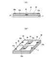
図1は、本発明の半導体積層パッケージの第1実施形態を示す縦断面図であり、図2〜図7はその製造方法の手順を説明する図、図8は配線拡張部の一例を示す平面図である。
図1に示すように、第1実施形態の半導体積層パッケージAは、平面視矩形状の第1のプリント配線板1の中央上部側に平面視矩形状の第1の半導体チップ2と第2の半導体チップ3と第2のプリント配線板(配線拡張部)4とを積層し、これらを覆って第1のプリント配線板1の上に封止用のモールド樹脂からなる封止体5が設けられ、第1のプリント配線板1の下面側に半田ボール6が複数設けられて構成されている。
前記第1のプリント配線板1は中央部にスリット状の配線用接続孔1aが形成され、その上面側周辺部に複数の接続ランド1bが形成され、第1のプリント配線板1の裏面側中央部の配線用接続孔1aの周辺部分にも接続ランド1dが複数形成されている。第1のプリント配線板1の内部には、各接続ランド1bあるいは接続ランド1dを半田ボール6の形成部分のいずれかに接続するための内部配線等が組み込まれているがそれらの詳細構造について図1では略している。
Hereinafter, the semiconductor stacked package of the best mode of the present invention will be described with reference to the drawings. However, the present invention is not limited to the following embodiments.
FIG. 1 is a longitudinal sectional view showing a first embodiment of a semiconductor stacked package according to the present invention, FIG. 2 to FIG. 7 are diagrams for explaining the procedure of the manufacturing method, and FIG. 8 is a plan view showing an example of a wiring extension portion. FIG.
As shown in FIG. 1, the semiconductor stacked package A of the first embodiment includes a
The first printed
前記第1の半導体チップ2は複数のパッド2bを第1のプリント配線板1の配線用接続孔1aに収容するように望ませた状態、即ち、複数のパッド2bを下向きとして第1のプリント配線板上に配置されている。
前記第2の半導体チップ3は前記第1の半導体チップ2と同等の構造であり、第2の半導体チップ3は複数のパッド3bを上向きとして、第1の半導体チップ2上に積層されている。前記半導体チップ2、3においてパッド2b、3bが形成されていない側の面は平面部2d、3dとされているので、図1の構造では第1の半導体チップ2の上に第2の半導体チップ3は密着配置されている。
The
The
前記半導体チップ3の上には、半導体チップ3と平面視形状が同等の矩形板状の配線拡張部(第2のプリント配線板)4が積層されている。この配線拡張部4は基板4aの中央部にスリット状の配線用孔部4bが形成され、この配線用孔部4b内に半導体チップ3の複数のパッド3bを望ませて、換言すると各パッド3bを配線用孔部4b内に収容するように配線拡張部4が半導体チップ3上に積層されている。
図8に配線拡張部4の一例を示すが、矩形状の基板4aの中央部に図8の縦方向に延在するスリット状の配線用孔部4bが形成されていて、図8ではこの配線用孔部4bを介してその下に複数(例えば29個の)のパッド3bが存在している状態を示す。
図8の例では29個のパッド3bのうち、半分程度のパッド3bが信号系のパッドであり、他のパッド3bは電源系のパッドあるいはグランド系のパッドとされている。
On the
FIG. 8 shows an example of the
In the example of FIG. 8, of the 29
図8の例では基板4aの上面側においてスリット状の配線用孔部4bの両側に整列するように短冊状の配線回路4d1、4d2が交互に4個ずつ8個、更に2列合わせて合計16個形成されている。ここで配線回路4dを8個ずつ形成したのは、半導体チップ3に形成されているパッド3bのうち、電源系のパッドとグランド系のパッドを全部配線するために必要な数を確保するためであり、これらの配線回路4dを設ける数は特に問わない。
図8においてより具体的には、薄く塗られている箇所の配線回路4d1は、電源系のパッド用の配線回路(例えばVDD,VDDQ)であり、ドットを多数形成して表記している配線回路4d2は、グランド系のパッド用の配線回路(例えば、VSS,VSSQ)であり、図8に示す配線拡張部(第2のプリント配線板)4は、片面にCu箔を設けた片面基板を例示している。
In the example of FIG. 8, eight strip-like wiring circuits 4d1 and 4d2 are alternately arranged so as to be aligned on both sides of the slit-
More specifically, in FIG. 8, the wiring circuit 4d1 in a thinly painted portion is a wiring circuit for a power supply pad (for example, VDD, VDDQ), and is a wiring circuit represented by forming a large number of dots. 4d2 is a wiring circuit for ground pads (for example, VSS, VSSQ), and the wiring extension part (second printed wiring board) 4 shown in FIG. 8 is an example of a single-sided board provided with Cu foil on one side. is doing.
前記半導体チップ3の29個のパッド3bのうち、電源系あるいはグランド系の16個のパッド3bがパッド3bと配線回路4d1と4d2の端部とを接続するワイヤー線8によりボンディング接続されている。また、ワイヤー線8が接続された配線回路4d1と4d2の反対側の端部とその外側に位置する第1のプリント配線板1の接続ランド1cはワイヤー線9によりワイヤーボンディング接続されている。なお、図8に示す配線拡張部4上の配線回路4d1(4d2)において配線用孔部4b側の端部に接続ランド4eが形成され、配線拡張部4の周縁部に近い側の配線回路4d1(4d2)の端部に接続ランド4fが形成され、具体的にはこれらの接続ランド4eまたは接続ランド4fにワイヤー線8またはワイヤー線9が接続されている。
次に、前記半導体チップ3の残り13個のパッドは信号系のパッド3bであるので、これらのパッド3bについては、配線用孔部4bと配線拡張部4の上方並びに側方を通過させて第1の配線板1上の接続パッド1bに到達可能な比較的長いワイヤー線10によりパッド3bと接続パッド1bとをワイヤーボンディング接続する。図8ではこれらのワイヤー線10を鎖線で示している。
Of the 29
Next, since the remaining 13 pads of the
次に、第1の半導体チップ2の複数のパッド2bは先に説明した如く第1のプリント配線板1のスリット状の配線用接続孔1aの内部側に望ませられているが、第1のプリント配線板1の裏面側において先の配線用接続孔1aの周辺部には接続ランド1dが複数配列形成され、これらの接続ランド1dに第1の半導体チップ1のパッド2bがワイヤー線11を用いてワイヤーボンディング接続され、これらの部分周り、即ち、配線用接続孔1aの内部とワイヤー線11とパッド2b、1dとその部分周りが封止材12により覆われて保護されている。
Next, the plurality of
以上説明した構造を採用してなる半導体積層パッケージAにおいては、上述の如く設けられたワイヤー線8は配線用孔部4bを通過させてパッド3bと短冊状の配線回路4dの端部との間で至近距離にて接続できるので、短いもので良い。また、ワイヤー線9においても配線回路の端部の接続ランド4fからその近傍に配置されている第1のプリント配線板1の接続ランド1cに接続するので短いもので良い。また、ワイヤー線8、9を接続する形で設けられる配線回路4d1、4d2にあっては、ワイヤー線8、9の径よりも充分に太い(例えばワイヤー径φ25μmに対してより太い配線の)導体層を利用できるので、配線インピーダンスを充分に低くすることができる。また、半導体チップ3の複数のパッド3bのうち、全数を配線回路に接続するのではなく、特に影響の大きい電源系、グランド系のパッド3bの配線のみを配線回路4d1、4d2に接続するので、配線拡張部4の表面積を有効利用して1つ1つの配線回路をできるだけ低インピーダンスのものとすることができる。
以上説明のようにワイヤー線8、9を短くできることから、これらのワイヤー線8、9での抵抗の増大は生じ難いし、インダクタンスの増加も少ないので、これらのワイヤー線8、9の部分でのノイズ発生の問題は生じ難く、電圧降下も抑制でき、第2の半導体チップ3の高速動作に支障を来さない。
In the semiconductor laminated package A adopting the structure described above, the
Since the
次に、図2〜図7を基に、図1に示す半導体積層パッケージAの製造方法の一例について説明する。
まず、第1のプリント配線板1の上面において第1の半導体チップ2を搭載する領域に絶縁性接着剤(例えばエポキシ樹脂やエラストマ材:図示略)を供給し、前記第1の半導体チップ2をその回路面(パッド2bの形成面)が下向きになるように前記第1のプリント配線板1の中央に搭載し、前記絶縁性接着剤を硬化させ、前記第1の半導体チップ2と前記第1のプリント配線板1を接着する。図2(A)はその状態を示す断面図である。
Next, an example of a method for manufacturing the semiconductor stacked package A shown in FIG. 1 will be described with reference to FIGS.
First, an insulating adhesive (for example, an epoxy resin or an elastomer material: not shown) is supplied to a region where the
前記第1のプリント配線板2は、図2(B)のように中央部にスリット状の配線用接続孔1aが形成されていて、第1の半導体チップ2の電極パッド部2bを配線用接続孔1a内に望ませた構造になっている。図2(B)は、前記第1の半導体チップ2を下向きになるように反転し、斜め上からみた図である。
次に、図3に示すように、前記第1の半導体チップ2の電極パッド2bから前記配線用接続孔1aを介し、前記第1のプリント配線板1において前記第1の半導体チップ2が搭載された逆面(裏面)に設けられた接続ランド1dへワイヤーボンディング法にて、例えば金(Au)からなるワイヤー線11を接続する。
図3(A)は、その断面図であり、図3(B)は、前記第1の半導体チップ2を下向きになるように反転し、斜め上からみた図である。
続いて、 前記第1の半導体チップ2の上(回路面とは逆面側の平面部2d)に絶縁性接着剤(例えばエポキシ樹脂やエラストマ材:図示略)を供給し、第2の半導体チップ3を回路面が上向きになるように搭載し、前記絶縁性接着剤を硬化させ、前記第1の半導体チップ2と前記第2の半導体チップ3を接着させる。ここで第1の半導体チップ2の平面部2dと第2の半導体チップ3の平面部3dが密着する。図4は、その断面図である。
As shown in FIG. 2B, the first printed
Next, as shown in FIG. 3, the
FIG. 3A is a cross-sectional view thereof, and FIG. 3B is a view of the
Subsequently, an insulating adhesive (for example, an epoxy resin or an elastomer material: not shown) is supplied onto the first semiconductor chip 2 (a
次に、前記第2の半導体チップ3の上(回路面側)に電源用とグランド用の配線回路のみ形成された第2のプリント配線板(配線拡張部)4を積層する領域に絶縁性接着剤(例えばエポキシ樹脂やエラストマ材:図示略)を供給し、図5のように前記第2の半導体チップ3の上(回路面側)に電源用とグランド用の配線回路のみ形成された第2のプリント配線板4を積層し、前記絶縁性接着剤を硬化させ、前記第2の半導体チップ3と電源とグランドのみ形成された第2のプリント配線板4を接着する。前記第2のプリント配線板4は、その中央部にスリット状の配線用孔部4bが形成されているので、前記第2の半導体チップ3の電極パッド3bは配線用孔部4bに望ませられた状態になっている。図5(A)はその状態の断面図であり、図5(B)は、斜め上からみた図である。
Next, insulative bonding is performed on a region where the second printed wiring board (wiring extension portion) 4 in which only the power and ground wiring circuits are formed on the second semiconductor chip 3 (circuit side) is laminated. An agent (for example, an epoxy resin or an elastomer material: not shown) is supplied, and only a power supply circuit and a ground wiring circuit are formed on the second semiconductor chip 3 (circuit side) as shown in FIG. The printed
次に、図6に示すように、前記第2の半導体チップ3の電源用とグランド用の電極パッド3bから前記電源用とグランド用の配線回路のみ形成された第2のプリント配線板4に設けられた接続ランド4eへワイヤーボンディング法にて、例えば金(Au)からなるワイヤー線8を接続する。図6(A)は、その状態の断面図であり、図6(B)は、斜め上からみた図である。
続いて図7に示すように、前記第2の半導体チップ3の信号系の電極パッド3bから前記電源用とグランド用の配線回路のみ形成された第2のプリント配線板4の配線用孔部4bを介し、前記第1のプリント配線板1の接続ランド1bへワイヤーボンディング法にて、例えば金(Au)からなるワイヤー線10で接続する。ここでワイヤー線10は配線拡張部4の上方と側方を通過して接続ランド1bへ到達する。更に、前記第2のプリント配線板4の端に設けられた接続ランド4fから前記第1のプリント配線板1の接続ランド1cへワイヤーボンディング法にて、例えば金(Au)からなるワイヤー9で接続する。
なお、図7(A)をはじめとする断面図では、接続ランド1bと1cは、図面上、便宜的に分けて配置(1cは半導体チップ寄り,1dは外側寄り)しているが、同一直線上でもよく、各図に示すように電源用、グランド用の接続ランド1cを半導体チップ寄りに配置するとワイヤー線の長さがより短くなるため、なお好ましい。図7(A)は、その状態の断面図であり、図7(B)は、斜め上からみた図である。
Next, as shown in FIG. 6, the second printed
Subsequently, as shown in FIG. 7, the
7A, the connection lands 1b and 1c are separately arranged for convenience in the drawing (1c is closer to the semiconductor chip and 1d is closer to the outer side). It may be on a wire, and as shown in each figure, it is more preferable to arrange the
最後に、図1のように、モールド材(例えば、エポキシ樹脂)にて、半導体チップ2、3やワイヤー線8、9、10を封止するとともに第1のプリント配線板1の上面側と第1第2の半導体チップ2,3を覆うように封止部5を構成する。更に第1のプリント配線板1の裏面側のワイヤー線11とその周囲の部分にもモールド材を充填して封止部12を形成する。また、半導体パッケージの電極となる半田ボール6(例えば、錫(Sn)、銀(Ag)、銅(Cu)からなる)を形成させ、半導体積層パッケージAを完成させることができる。
Finally, as shown in FIG. 1, the
図9は本発明の第2実施形態を示すもので、本実施形態の半導体積層パッケージBにおいては、図9に示すように、第2の半導体チップ3の信号系のパッド3bから第1のプリント配線板1の接続ランド1cへ接続させるワイヤー線15は、配線拡張部4を積層する前にワイヤーボンディング接続し、前記ワイヤー線15が埋まる程度、第2の半導体チップ3の回路面側に絶縁性接着剤16(例えば、エポキシ樹脂などの絶縁層)を供給して絶縁層とし、前記ワイヤー線15と絶縁性接着剤16の上に前記配線拡張部4を積層した構造としたものである。ここで絶縁性接着剤16は第2の半導体チップ3においてパッド3bが形成されている部分は設けないようにする。即ち、第2の半導体チップ3においてパッド3bは絶縁接着剤16の無い透孔部16aを介して配線拡張部4の配線用孔部4bに望ませられている。また、絶縁性接着剤16の無い透孔部16aにはモールド樹脂が充填されて封止材により保護されている。なお、図9の構造においてその他の部分の構造は先の第1の実施の形態の半導体積層パッケージAと同等である。
本実施形態の構造であっても、先の形態と同様の効果が得られる。
FIG. 9 shows a second embodiment of the present invention. In the semiconductor stacked package B of the present embodiment, as shown in FIG. 9, the first print is started from the
Even with the structure of the present embodiment, the same effect as the previous embodiment can be obtained.
図10は本発明の第3実施形態を示すもので、本実施形態の半導体積層パッケージCにおいて、図10に示すように、第1のプリント配線板1に対して第1の半導体チップ2をフェイスダウン状態(パッド2bを有する回路面が下向き)に設置し、第1のプリント配線板1Aの中央部上に形成した複数の接続ランド1eに各パッド2bを直接接続し、それらの周囲であって第1のプリント基板1Aと第1の半導体チップ2との間に絶縁樹脂層(絶縁層)18を配置して実装した構造(フリップチップ実装構造)であっても、同様の効果が得られる。
なお、図10の構造においてその他の部分は先の第1の実施の形態の半導体積層パッケージAと同等である。
FIG. 10 shows a third embodiment of the present invention. In the semiconductor stacked package C of this embodiment, the
In the structure of FIG. 10, the other parts are the same as those of the semiconductor stacked package A of the first embodiment.
図11は本発明の第4実施形態を示すもので、本実施形態の半導体積層パッケージDにおいて、第1のプリント配線板1に対して第1の半導体チップ2をフェイスアップ状態(パッド2bを設けた回路面を上向き)に搭載し、前記第1の半導体チップ2の上に電源用、グランド用の配線回路のみ形成された配線拡張部4を積層し、前記第1の半導体チップ2の電源系あるいはグランド系のパッド2bから前記電源用とグランド用の配線回路のみ形成された配線拡張部4に設けられた接続ランド4eへ短いワイヤー線8で接続し、前記第1の半導体チップ2の信号系のパッド2bから前記配線拡張部4の配線用孔部4bを介し、前記第1のプリント配線板1の接続ランド1cへワイヤー線10で接続する。
更に、前記配線拡張部4の端に設けられた接続ランド4fから前記第1のプリント配線板1の接続ランド1cへ短いワイヤー線9で接続する。次に、前記ワイヤー線10が埋まるくらいに前記第1の半導体チップ2の回路面側に絶縁性接着剤(絶縁層)20(例えば、エポキシ樹脂)を供給し、その上に第2の半導体チップ3を搭載し、前記絶縁性接着剤20を硬化させる。
FIG. 11 shows a fourth embodiment of the present invention. In the semiconductor stacked package D of the present embodiment, the
Further, the
更にその上に第2の半導体チップ3を積層し、更に電源系とグランド系の配線回路のみ形成された配線拡張部4をもう一枚積層した構造にすることにより、先の実施の形態と同様の効果が得られる。なお、図11の構造においてその他の部分は先の実施形態の半導体積層パッケージと同等である。
Further, the
ところで、図1、9、10、11に示す各実施形態の構造において、電源用とグラウンド用の配線回路のみ形成された配線拡張部4は、Cu箔が両面に形成されている両面基板であれば、電源用とグランド用の配線回路の回路幅をより太くすることが可能となり、且つ電源用とグランド用の配線回路を別の層に分けて形成すれば、電源用の配線回路とグランド用の配線回路間で生じる相互インダクタンスより、実効インダクタンスが低くなるので、なお好ましい構造となる。また、図1、9、10、11に示す構造において、電源用とグラウンド用の配線回路のみ形成された配線拡張部4は、複数ある電源パターン用の配線回路4d1またはグランドパターン用の配線回路4d2を結合(例えば、VDDパターンをひとまとめにベタパターンとする)することが可能であり、その場合は更にインピーダンスを小さくすることが可能である。
更に、図1、9、10、11に示す各実施形態の構造において、電源用とグラウンド用配線回路のみ形成された配線拡張部4は、電源をVDD,VDDQに結合し、同様にグランドをVSS,VSSQに結合すれば、更に大きなベタパターンを配線回路として形成することが可能になり、更にインピーダンスを小さくすることが可能である。
By the way, in the structure of each embodiment shown in FIGS. 1, 9, 10, and 11, the
Further, in the structure of each embodiment shown in FIGS. 1, 9, 10 and 11, the
以上説明した本発明の各実施形態に代えて、配線拡張部4を用意する代りに、ウェハーレベルCSP(Chip Size Package)の再配線形成の製造方法を用いて、半導体チップ上に直接配線層を形成することも可能である。
ウェハーレベルチップサイズパッケージとは、半導体ウェハー上に半導体チップを形成した後に、半導体ウェハーの状態で配線(再配線層)や保護膜、接続ランドの形成を行い、その後にダイシングにより各半導体チップに個片化する製造方法のことである。
本発明における、電源用とグランド用のみ形成された配線拡張部(第2のプリント配線板)4の代わりに電源用とグランド用の回路配線のみを形成したウェハーレベルチップサイズパッケージとしての再配線層(配線拡張部)の構造を採用してもなおインピーダンスを小さくすることが可能である。
具体的には図12に示す如く、再配線層25として、第2の半導体チップ3の上面において複数のパッド3b形成部分を除いて絶縁層25Aで覆い、電源系とグランド系の各パッド3bの部分から第2の半導体チップ3の周辺部分まで配線層24を個々のパッド用に延出形成し、第2の半導体チップ3の周辺部に接続ランド24aを設けた構造を例示することができる。
図12に示す例では更に配線用孔部25aが再配線層25の間に複数形成され、配線用孔部25aの内部には第2の半導体チップ3の信号系のパッド3bが望ませられている。この構造の再配線層25を第2の半導体チップ3の上に形成したものをここではウェハーレベルチップサイズパッケージチップ26と称する。
Instead of preparing the
A wafer level chip size package is a semiconductor chip formed on a semiconductor wafer, followed by the formation of wiring (redistribution layer), protective film, and connection land in the state of the semiconductor wafer, and then dicing to each semiconductor chip. It is a manufacturing method that separates pieces.
Rewiring layer as a wafer level chip size package in which only circuit wiring for power supply and ground is formed instead of wiring extension part (second printed wiring board) 4 formed only for power supply and ground in the present invention Even if the (wiring extension) structure is adopted, the impedance can still be reduced.
Specifically, as shown in FIG. 12, as the
In the example shown in FIG. 12, a plurality of
この実施形態の製造方法としては、先に説明した図4の工程に代えて、図12に示すように、第2の半導体チップ3に対しウェハーレベルチップサイズパッケージの製造プロセスにて、再配線層25に電源用とグランド用のみ形成した配線24を設けたウェハーレベルチップサイズパッケージチップ26を製作して適用する。また、前記第2の半導体チップ3の信号系の電極パッド3b部は、再配線層25がくり貫かれて配線用孔部25aが形成されている部分に対応させて配置されている。図12(A)は、その断面図であり、図12(B)は、斜め上からみた図である。
As a manufacturing method of this embodiment, in place of the process of FIG. 4 described above, as shown in FIG. 12, a rewiring layer is manufactured by a wafer level chip size package manufacturing process for the
次に、図13に示すように、第1の半導体チップ2の上(回路面とは逆面)に絶縁性接着剤(例えばエポキシ樹脂やエラストマ材:図示略)を供給し、前記ウェハーレベルチップサイズパッケージチップ26を第2の半導体チップ3が下になるように搭載し、前記絶縁性接着剤を硬化させ、前記第1の半導体チップ2と前記ウェハーレベルチップサイズパッケージチップ26を接着させる。図13(A)は、その断面図であり、図13(B)は、斜め上からみた図である。
Next, as shown in FIG. 13, an insulating adhesive (for example, epoxy resin or elastomer material: not shown) is supplied onto the first semiconductor chip 2 (opposite to the circuit surface), and the wafer level chip is then supplied. The
次に、図14に示すように、前記第2の半導体チップ3の信号系の電極パッド3bから前記電源用とグランド用の配線回路のみ形成された再配線層25の配線用孔部25aを介し、第2の半導体チップ3の上方と側方を通過するようにして前記第1のプリント配線板1の接続ランド1bへワイヤーボンディング法にて、例えば金(Au)からなるワイヤー線10で接続する。
更に前記電源用とグランド用のみ回路配線が形成された再配線層25の端に設けられた接続ランド24aから前記第1のプリント配線板1の接続ランド1cへワイヤーボンディング法にて、例えば金(Au)からなるワイヤー線9で接続する。図14(A)は、その状態の断面図であり、図14(B)は、斜め上からみた図である。
Next, as shown in FIG. 14, through the
Further, the
上記の構造は、電源用とグランド用の配線回路のみ形成された配線拡張部4の代わりに電源用とグランド用の回路配線のみを形成したウェハーレベルチップサイズパッケージのような再配線層25を採用すれば、先の実施形態で設けられていたワイヤー線8を再配線24に代えることより、更にインピーダンスを小さくすることが可能である。
また、図10に示した第3の実施形態において、電源用とグランド用のみ形成された配線拡張部(第2のプリント配線板)4の代わりに電源用とグランド用の回路配線のみを形成したウェハーレベルチップサイズパッケージとしての前述の再配線層25に代えても、同様の効果が得られる。
更に図11に示す第4の実施形態において、第1の半導体チップ2及び第2の半導体チップ3の上に積層している電源用とグランド用の回路配線のみ形成された配線拡張部(第2のプリント配線板)4の代わりに電源用とグランド用の回路配線のみを形成したウェハーレベルチップサイズパッケージとしての前述の再配線層25に代えても、同様の効果が得られる。
The above structure employs a
Further, in the third embodiment shown in FIG. 10, only the power supply and ground circuit wirings are formed instead of the wiring extension portion (second printed wiring board) 4 formed only for the power supply and the ground. Even if the
Furthermore, in the fourth embodiment shown in FIG. 11, a wiring extension (second wiring) formed only on the circuit wiring for power supply and ground that is laminated on the
本発明の活用例として、中央部に電極パッドやグランド系のパッドが配置されている汎用DRAMなどの各種半導体チップによる半導体積層パッケージ全般に適用することができ、その半導体積層パッケージはDRAMを1つの適用例として用いることができる。なお、本発明の半導体積層パッケージをデータプロセッサやROM(Read Only Memory)など、他の種々の半導体チップの積層構造に広く適用できるのは勿論である。 As an application example of the present invention, the present invention can be applied to general semiconductor stacked packages using various semiconductor chips such as a general-purpose DRAM in which an electrode pad and a ground pad are arranged at the center. It can be used as an application example. Of course, the semiconductor stacked package of the present invention can be widely applied to stacked structures of various other semiconductor chips such as a data processor and a ROM (Read Only Memory).
A、B、C、D…半導体積層パッケージ、
1…第1のプリント配線板、1a…配線用接続孔、1b、1c、1d、1e…接続ランド、2…第1の半導体チップ、2b…パッド、2d…第1の半導体チップの平面部、3…第2の半導体チップ、3b…パッド、3d…第2の半導体チップの平面部、4…配線拡張部(第2のプリント配線板)、4a…基板、4b…配線用孔部、4d1、4d2…配線回路、4e、4f…接続ランド、5…封止材、6…半田ボール、8、9、10、11、15…ワイヤー線、16…絶縁接着層、18…絶縁樹脂層、20…絶縁性接着剤(絶縁層)、24…配線層、25…再配線層、24a…接続ランド、
A, B, C, D ... Semiconductor stacked package,
DESCRIPTION OF
Claims (13)
中央に配線用孔部を有する配線拡張部が前記配線用孔部を前記上段の半導体チップの電源系のパッドとグランド系のパッドと信号系のパッドに望ませて前記上段の半導体チップ上に積層され、該配線拡張部にはその中央部側からその周辺部側にかけて延出形成された配線回路が設けられる一方、
前記上段の半導体チップの電源系のパッドとグランド系のパッドが前記配線拡張部の中央部側の配線回路に接続されるとともに、
前記配線拡張部の周辺部側の配線回路がワイヤー線を介して前記第1のプリント配線板上の接続ランドにボンディング接続されてなることを特徴とする半導体積層パッケージ。 A plurality of semiconductor chips are stacked on the first printed wiring board, and among these semiconductor chips, the upper semiconductor chip is provided with a power supply pad, a ground pad, and a signal pad in the center on the upper surface side. A semiconductor stacked package in which connection lands are formed around a portion where the semiconductor chips are stacked in the first printed wiring board,
A wiring extension having a wiring hole in the center is stacked on the upper semiconductor chip in a manner that the wiring hole is desired for the power supply pad, ground pad and signal pad of the upper semiconductor chip. The wiring extension portion is provided with a wiring circuit formed extending from the central side to the peripheral side,
The power supply system pad and the ground system pad of the upper semiconductor chip are connected to the wiring circuit on the center side of the wiring extension,
A semiconductor stacked package, wherein a wiring circuit on a peripheral side of the wiring extension portion is bonded to a connection land on the first printed wiring board via a wire.
Priority Applications (2)
| Application Number | Priority Date | Filing Date | Title |
|---|---|---|---|
| JP2007199695A JP2009038142A (en) | 2007-07-31 | 2007-07-31 | Semiconductor stacked package |
| US12/219,839 US7777350B2 (en) | 2007-07-31 | 2008-07-29 | Semiconductor stack package having wiring extension part which has hole for wiring |
Applications Claiming Priority (1)
| Application Number | Priority Date | Filing Date | Title |
|---|---|---|---|
| JP2007199695A JP2009038142A (en) | 2007-07-31 | 2007-07-31 | Semiconductor stacked package |
Publications (1)
| Publication Number | Publication Date |
|---|---|
| JP2009038142A true JP2009038142A (en) | 2009-02-19 |
Family
ID=40337356
Family Applications (1)
| Application Number | Title | Priority Date | Filing Date |
|---|---|---|---|
| JP2007199695A Pending JP2009038142A (en) | 2007-07-31 | 2007-07-31 | Semiconductor stacked package |
Country Status (2)
| Country | Link |
|---|---|
| US (1) | US7777350B2 (en) |
| JP (1) | JP2009038142A (en) |
Cited By (8)
| Publication number | Priority date | Publication date | Assignee | Title |
|---|---|---|---|---|
| JP2011096851A (en) * | 2009-10-29 | 2011-05-12 | Sony Corp | Semiconductor device, manufacturing method thereof, and electronic apparatus |
| JP2011159958A (en) * | 2010-01-08 | 2011-08-18 | Sony Corp | Semiconductor device, solid-state imaging apparatus, and camera system |
| US8331182B2 (en) | 2009-09-15 | 2012-12-11 | Elipida Memory, Inc. | Semiconductor device including plural electrode pads |
| US8587097B2 (en) | 2009-06-11 | 2013-11-19 | Elpida Memory Inc. | Semiconductor device that suppresses malfunctions due to noise generated in internal circuit |
| US8633596B2 (en) | 2010-11-11 | 2014-01-21 | Mitsuaki Katagiri | Semiconductor package with bonding wires of reduced loop inductance |
| US9633980B2 (en) | 2015-05-29 | 2017-04-25 | Kabushiki Kaisha Toshiba | Semiconductor device |
| JP2020145407A (en) * | 2019-03-04 | 2020-09-10 | エスケーハイニックス株式会社SK hynix Inc. | Laminated semiconductor package with wire bonding connection structure |
| JP2021044458A (en) * | 2019-09-12 | 2021-03-18 | キヤノン株式会社 | Wiring substrate and semiconductor apparatus |
Families Citing this family (11)
| Publication number | Priority date | Publication date | Assignee | Title |
|---|---|---|---|---|
| SG130066A1 (en) * | 2005-08-26 | 2007-03-20 | Micron Technology Inc | Microelectronic device packages, stacked microelectronic device packages, and methods for manufacturing microelectronic devices |
| US8014166B2 (en) * | 2008-09-06 | 2011-09-06 | Broadpak Corporation | Stacking integrated circuits containing serializer and deserializer blocks using through silicon via |
| JP5557439B2 (en) * | 2008-10-24 | 2014-07-23 | ピーエスフォー ルクスコ エスエイアールエル | Semiconductor device and manufacturing method thereof |
| JP2010192680A (en) * | 2009-02-18 | 2010-09-02 | Elpida Memory Inc | Semiconductor device |
| US20110084374A1 (en) * | 2009-10-08 | 2011-04-14 | Jen-Chung Chen | Semiconductor package with sectioned bonding wire scheme |
| JP2011249582A (en) * | 2010-05-27 | 2011-12-08 | Elpida Memory Inc | Semiconductor device |
| US9136197B2 (en) | 2010-09-16 | 2015-09-15 | Tessera, Inc. | Impedence controlled packages with metal sheet or 2-layer RDL |
| US8853708B2 (en) * | 2010-09-16 | 2014-10-07 | Tessera, Inc. | Stacked multi-die packages with impedance control |
| KR101061531B1 (en) * | 2010-12-17 | 2011-09-01 | 테세라 리써치 엘엘씨 | Enhanced stacked microelectronic assemblies with central contacts and improved ground or power distribution |
| US10062676B1 (en) * | 2017-05-25 | 2018-08-28 | Hsiu Hui Yeh | Multilayer chipset structure |
| US20210118838A1 (en) * | 2019-10-16 | 2021-04-22 | Nanya Technology Corporation | Chip-package device |
Citations (10)
| Publication number | Priority date | Publication date | Assignee | Title |
|---|---|---|---|---|
| JP2002118197A (en) * | 2000-10-05 | 2002-04-19 | Hitachi Cable Ltd | Wiring board, semiconductor device using the same, and method of manufacturing the same |
| US6472736B1 (en) * | 2002-03-13 | 2002-10-29 | Kingpak Technology Inc. | Stacked structure for memory chips |
| US20030124766A1 (en) * | 2001-12-29 | 2003-07-03 | Kim Ji Yon | Method for manufacturing stacked chip package |
| JP2004214522A (en) * | 2003-01-08 | 2004-07-29 | Ibiden Co Ltd | Component built-in module |
| JP2004327993A (en) * | 2003-04-26 | 2004-11-18 | Samsung Electronics Co Ltd | Multi-chip BGA package |
| JP2004327652A (en) * | 2003-04-24 | 2004-11-18 | Renesas Technology Corp | Semiconductor device and method of manufacturing the same |
| JP2005033201A (en) * | 2003-07-04 | 2005-02-03 | Samsung Electronics Co Ltd | Semiconductor package |
| JP2005150719A (en) * | 2003-11-13 | 2005-06-09 | Samsung Electronics Co Ltd | Double stacked BGA package and multiple stacked BGA package |
| JP2005167222A (en) * | 2003-11-15 | 2005-06-23 | Samsung Electronics Co Ltd | Semiconductor chip package and method for connecting substrate and semiconductor chip |
| WO2007025127A2 (en) * | 2005-08-26 | 2007-03-01 | Micron Technology, Inc. | Microelectronic device packages, stacked microlecetronic device packages, and methods for manufacturing microelectronic devices |
Family Cites Families (8)
| Publication number | Priority date | Publication date | Assignee | Title |
|---|---|---|---|---|
| US5719436A (en) | 1995-03-13 | 1998-02-17 | Intel Corporation | Package housing multiple semiconductor dies |
| JP3937265B2 (en) | 1997-09-29 | 2007-06-27 | エルピーダメモリ株式会社 | Semiconductor device |
| JP3053013B2 (en) | 1998-04-01 | 2000-06-19 | 日本電気株式会社 | Semiconductor integrated circuit device |
| JP2001085609A (en) | 1999-09-17 | 2001-03-30 | Hitachi Ltd | Semiconductor device and method of manufacturing the same |
| JP2002208656A (en) * | 2001-01-11 | 2002-07-26 | Mitsubishi Electric Corp | Semiconductor device |
| US6555919B1 (en) * | 2002-04-23 | 2003-04-29 | Ultratera Corporation | Low profile stack semiconductor package |
| DE10259221B4 (en) * | 2002-12-17 | 2007-01-25 | Infineon Technologies Ag | Electronic component comprising a stack of semiconductor chips and method of making the same |
| KR100621991B1 (en) * | 2003-01-03 | 2006-09-13 | 삼성전자주식회사 | Chip scale stack package |
-
2007
- 2007-07-31 JP JP2007199695A patent/JP2009038142A/en active Pending
-
2008
- 2008-07-29 US US12/219,839 patent/US7777350B2/en active Active
Patent Citations (10)
| Publication number | Priority date | Publication date | Assignee | Title |
|---|---|---|---|---|
| JP2002118197A (en) * | 2000-10-05 | 2002-04-19 | Hitachi Cable Ltd | Wiring board, semiconductor device using the same, and method of manufacturing the same |
| US20030124766A1 (en) * | 2001-12-29 | 2003-07-03 | Kim Ji Yon | Method for manufacturing stacked chip package |
| US6472736B1 (en) * | 2002-03-13 | 2002-10-29 | Kingpak Technology Inc. | Stacked structure for memory chips |
| JP2004214522A (en) * | 2003-01-08 | 2004-07-29 | Ibiden Co Ltd | Component built-in module |
| JP2004327652A (en) * | 2003-04-24 | 2004-11-18 | Renesas Technology Corp | Semiconductor device and method of manufacturing the same |
| JP2004327993A (en) * | 2003-04-26 | 2004-11-18 | Samsung Electronics Co Ltd | Multi-chip BGA package |
| JP2005033201A (en) * | 2003-07-04 | 2005-02-03 | Samsung Electronics Co Ltd | Semiconductor package |
| JP2005150719A (en) * | 2003-11-13 | 2005-06-09 | Samsung Electronics Co Ltd | Double stacked BGA package and multiple stacked BGA package |
| JP2005167222A (en) * | 2003-11-15 | 2005-06-23 | Samsung Electronics Co Ltd | Semiconductor chip package and method for connecting substrate and semiconductor chip |
| WO2007025127A2 (en) * | 2005-08-26 | 2007-03-01 | Micron Technology, Inc. | Microelectronic device packages, stacked microlecetronic device packages, and methods for manufacturing microelectronic devices |
Cited By (13)
| Publication number | Priority date | Publication date | Assignee | Title |
|---|---|---|---|---|
| US8587097B2 (en) | 2009-06-11 | 2013-11-19 | Elpida Memory Inc. | Semiconductor device that suppresses malfunctions due to noise generated in internal circuit |
| US8331182B2 (en) | 2009-09-15 | 2012-12-11 | Elipida Memory, Inc. | Semiconductor device including plural electrode pads |
| US8848075B2 (en) | 2009-10-29 | 2014-09-30 | Sony Corporation | Semiconductor device, manufacturing method thereof, and electronic apparatus |
| JP2011096851A (en) * | 2009-10-29 | 2011-05-12 | Sony Corp | Semiconductor device, manufacturing method thereof, and electronic apparatus |
| US9093363B2 (en) | 2010-01-08 | 2015-07-28 | Sony Corporation | Semiconductor device, solid-state image sensor and camera system for reducing the influence of noise at a connection between chips |
| JP2011159958A (en) * | 2010-01-08 | 2011-08-18 | Sony Corp | Semiconductor device, solid-state imaging apparatus, and camera system |
| US8633596B2 (en) | 2010-11-11 | 2014-01-21 | Mitsuaki Katagiri | Semiconductor package with bonding wires of reduced loop inductance |
| US9595489B2 (en) | 2010-11-11 | 2017-03-14 | Longitude Semiconductor S.A.R.L. | Semiconductor package with bonding wires of reduced loop inductance |
| US9633980B2 (en) | 2015-05-29 | 2017-04-25 | Kabushiki Kaisha Toshiba | Semiconductor device |
| JP2020145407A (en) * | 2019-03-04 | 2020-09-10 | エスケーハイニックス株式会社SK hynix Inc. | Laminated semiconductor package with wire bonding connection structure |
| JP7474044B2 (en) | 2019-03-04 | 2024-04-24 | エスケーハイニックス株式会社 | STACKED SEMICONDUCTOR PACKAGE HAVING WIRE BONDING CONNECTION STRUCTURE - Patent application |
| JP2021044458A (en) * | 2019-09-12 | 2021-03-18 | キヤノン株式会社 | Wiring substrate and semiconductor apparatus |
| JP7362380B2 (en) | 2019-09-12 | 2023-10-17 | キヤノン株式会社 | Wiring boards and semiconductor devices |
Also Published As
| Publication number | Publication date |
|---|---|
| US7777350B2 (en) | 2010-08-17 |
| US20090032973A1 (en) | 2009-02-05 |
Similar Documents
| Publication | Publication Date | Title |
|---|---|---|
| JP2009038142A (en) | Semiconductor stacked package | |
| JP4808408B2 (en) | Multi-chip package, semiconductor device used for the same, and manufacturing method thereof | |
| JP4751351B2 (en) | Semiconductor device and semiconductor module using the same | |
| KR101070913B1 (en) | Stacked die package | |
| US8421244B2 (en) | Semiconductor package and method of forming the same | |
| US8253231B2 (en) | Stacked integrated circuit package using a window substrate | |
| JP2007251145A (en) | Stacked package | |
| JP2009044110A (en) | Semiconductor device and manufacturing method thereof | |
| KR20090050810A (en) | Stacked semiconductor package with improved junction reliability | |
| JP2011155203A (en) | Semiconductor device | |
| US8008765B2 (en) | Semiconductor package having adhesive layer and method of manufacturing the same | |
| CN101872757A (en) | Cavity chip package structure and package-on-package structure using the same | |
| JP4538830B2 (en) | Semiconductor device | |
| KR101078741B1 (en) | Semiconductor package and stacked semiconductor package having thereof | |
| JP4635202B2 (en) | Method for manufacturing double-sided electrode package | |
| TWI442522B (en) | Pocket chip package structure and stacked package structure using recessed chip package structure | |
| WO2014203739A1 (en) | Semiconductor device and method for manufacturing same | |
| JP3838907B2 (en) | Semiconductor device | |
| JP4090348B2 (en) | Built-in module | |
| JP2014120501A (en) | Semiconductor device and method for manufacturing the same | |
| KR101169688B1 (en) | Semiconductor Devices and Laminated Semiconductor Packages | |
| JP2014027145A (en) | Semiconductor device | |
| JP2010177530A (en) | Semiconductor device | |
| KR100400827B1 (en) | semiconductor package | |
| KR20010111602A (en) | Wire bonding structure between semiconductor chip and substrate, and semiconductor package using it, and manufacturing method of the same |
Legal Events
| Date | Code | Title | Description |
|---|---|---|---|
| A621 | Written request for application examination |
Free format text: JAPANESE INTERMEDIATE CODE: A621 Effective date: 20100614 |
|
| A977 | Report on retrieval |
Free format text: JAPANESE INTERMEDIATE CODE: A971007 Effective date: 20120127 |
|
| A131 | Notification of reasons for refusal |
Free format text: JAPANESE INTERMEDIATE CODE: A131 Effective date: 20120306 |
|
| A711 | Notification of change in applicant |
Free format text: JAPANESE INTERMEDIATE CODE: A711 Effective date: 20140225 |
|
| A02 | Decision of refusal |
Free format text: JAPANESE INTERMEDIATE CODE: A02 Effective date: 20140603 |