JP2009008869A - Liquid crystal display device, driving circuit and driving method thereof - Google Patents
Liquid crystal display device, driving circuit and driving method thereof Download PDFInfo
- Publication number
- JP2009008869A JP2009008869A JP2007169868A JP2007169868A JP2009008869A JP 2009008869 A JP2009008869 A JP 2009008869A JP 2007169868 A JP2007169868 A JP 2007169868A JP 2007169868 A JP2007169868 A JP 2007169868A JP 2009008869 A JP2009008869 A JP 2009008869A
- Authority
- JP
- Japan
- Prior art keywords
- common electrode
- common
- signal lines
- electrodes
- scanning signal
- Prior art date
- Legal status (The legal status is an assumption and is not a legal conclusion. Google has not performed a legal analysis and makes no representation as to the accuracy of the status listed.)
- Pending
Links
Images


Landscapes
- Liquid Crystal (AREA)
- Liquid Crystal Display Device Control (AREA)
- Control Of Indicators Other Than Cathode Ray Tubes (AREA)
Abstract
【課題】制振材などの部材を要することなく、駆動信号に起因する音鳴りを防止することのできる液晶表示装置を提供することを目的とする。
【解決手段】液晶層を介して各画素形成部との間に電圧を印加するために、それぞれが1以上の走査信号線と対応するk個に分割された共通電極14(1)〜14(k)を備える。各共通電極は隣接して配置されている他の共通電極のひとつと対になり、一対の共通電極を構成する互いに隣接する2つの共通電極のそれぞれには互いに逆の極性となる共通電極駆動信号が共通電極駆動回路24によって与えられる。
【選択図】図1An object of the present invention is to provide a liquid crystal display device capable of preventing sound generation caused by a drive signal without requiring a member such as a vibration damping material.
In order to apply a voltage between each pixel formation portion via a liquid crystal layer, each of the common electrodes is divided into k pieces corresponding to one or more scanning signal lines. k). Each common electrode is paired with one of the other common electrodes arranged adjacent to each other, and each of the two adjacent common electrodes constituting the pair of common electrodes has a common electrode drive signal having opposite polarities. Is provided by the common electrode drive circuit 24.
[Selection] Figure 1
Description
本発明は、液晶表示装置に関し、特に、携帯電話等に採用されている小型の液晶表示装置において振動を防止するための技術に関する。 The present invention relates to a liquid crystal display device, and more particularly to a technique for preventing vibration in a small liquid crystal display device employed in a mobile phone or the like.
従来より、スイッチング素子としてTFT(Thin Film Transistor:薄膜トランジスタ)を備えるアクティブマトリクス型液晶表示装置が知られている。この液晶表示装置は、互いに対向する2枚の絶縁性の基板から構成される液晶パネルを備えている。液晶パネルの一方の基板には、複数の走査信号線(ゲートバスライン)と複数の映像信号線(ソースバスライン)とが格子状に配置され、それら複数の走査信号線と複数の映像信号線との交差点にそれぞれ対応してマトリクス状に配置された複数の画素形成部が設けられている。図14は2行×2列分の画素形成部の等価回路を示す回路図である。図14に示すように、走査信号線GLと映像信号線SLとの交差部近傍にTFT11が設けられている。TFT11は、走査信号線GLに接続されたゲート電極、映像信号線SLに接続されたソース電極、およびドレイン電極とから構成される。ドレイン電極は、画像を形成するために基板上にマトリクス状に配置された画素電極12と接続されている。液晶パネルの他方の基板には、液晶層13を介して画素電極12との間に電圧を印加するための電極(以下「共通電極」という)14が、複数の画素形成部に共通的に設けられている。そして、画素電極12と液晶層13と共通電極14とによって液晶容量が形成されている。また、必要に応じて、液晶容量に並列に補助容量(不図示)が付加されている。このような構成において、各TFT11のゲート電極が走査信号線GLからアクティブな走査信号(ゲート信号)を受けたときに当該TFT11のソース電極が映像信号線SLから受ける映像信号(ソース信号)と、共通電極14に与えられる共通電極駆動信号とに基づいて、各画素形成部の液晶層13に電圧が印加される。これにより液晶が駆動され、画面上に所望の画像が表示される。
2. Description of the Related Art Conventionally, an active matrix type liquid crystal display device including a TFT (Thin Film Transistor) as a switching element is known. This liquid crystal display device includes a liquid crystal panel composed of two insulating substrates facing each other. On one substrate of the liquid crystal panel, a plurality of scanning signal lines (gate bus lines) and a plurality of video signal lines (source bus lines) are arranged in a lattice pattern, and the plurality of scanning signal lines and the plurality of video signal lines are arranged. There are provided a plurality of pixel forming portions arranged in a matrix corresponding to the intersections. FIG. 14 is a circuit diagram showing an equivalent circuit of a pixel formation portion for 2 rows × 2 columns. As shown in FIG. 14, a
ところで、液晶には、直流電圧が加わり続けると劣化するという性質がある。このため、液晶表示装置では、液晶層13には交流電圧が印加される。これについて、図15および図16を参照しつつ説明する。
By the way, the liquid crystal has a property of deteriorating when a DC voltage is continuously applied. For this reason, in the liquid crystal display device, an AC voltage is applied to the
図15は、アクティブマトリクス型液晶表示装置の液晶パネルの断面を模式的に示した図である。図15に示すように、液晶パネルは、TFTガラス基板15と画素電極12と液晶層13と共通電極14とCF(Color Filter)ガラス基板16とによって構成されている。この液晶層13への交流電圧の印加は、例えば、上述した各画素形成部において液晶層13に印加される電圧の極性を1フレーム期間毎に反転させることにより実現される。具体的には、共通電極14の電位を基準とした場合のソース電極の電圧(映像信号電圧)の極性が1フレーム期間毎に反転するように、液晶表示装置の駆動が行われている。なお、1フレーム期間とは、液晶表示装置の全ての画素形成部において液晶層13への電圧の印加が行われ、1画面分の画像が画面上に表示されるのに要する期間である。
FIG. 15 is a diagram schematically showing a cross section of a liquid crystal panel of an active matrix liquid crystal display device. As shown in FIG. 15, the liquid crystal panel includes a TFT glass substrate 15, a
上述のような液晶表示装置の駆動を実現する技術として、例えば、ライン反転駆動と呼ばれる駆動方式が知られている。図16は、駆動方式としてライン反転駆動が採用されている液晶表示装置における信号波形図である。図16において、符号THn(TH1、TH2、TH3、・・・)はn行目の走査信号線が選択されている期間を示し、符号TFは1フレーム期間を示している。映像信号Vsは、図16に示すように、1水平走査期間毎に極性が反転し、さらに、1フレーム期間毎にも極性が反転している。同様に、共通電極を駆動する共通電極駆動信号Vcomも、1水平走査期間毎に極性が反転し、さらに、1フレーム期間毎にも極性が反転している。これにより、液晶層13に印加される電圧の極性が1水平走査期間毎に反転し、液晶表示装置の交流駆動が実現されている。
As a technique for realizing driving of the liquid crystal display device as described above, for example, a driving method called line inversion driving is known. FIG. 16 is a signal waveform diagram in a liquid crystal display device in which line inversion driving is adopted as a driving method. In FIG. 16, symbol THn (TH1, TH2, TH3,...) Indicates a period in which the n-th scanning signal line is selected, and symbol TF indicates one frame period. As shown in FIG. 16, the polarity of the video signal Vs is inverted every horizontal scanning period, and the polarity is inverted every frame period. Similarly, the polarity of the common electrode drive signal Vcom for driving the common electrode is inverted every horizontal scanning period, and further, the polarity is inverted every frame period. As a result, the polarity of the voltage applied to the
近年、上述のような液晶表示装置は、携帯電話等の電子機器のメイン画面として多く採用されている。例えば、このような液晶表示装置の1つに、320×240の解像度をもつQVGA(Quarter Video Graphics Array)と呼ばれる規格のものがある。このようなQVGA型クラスの解像度を持つ液晶表示装置において、上述のような交流駆動に起因して、図15に示したCFガラス基板16が振動し、その振動が耳障りな音として感じられることが指摘されている。このような振動による耳障りな音の発生(以下、「音鳴り」という。)を防止するための従来技術としては、以下のようなものが知られている。なお、音鳴りは、共通電極14の電位の反転する頻度を表す周波数(以下、「共通電極電位反転周波数」という。)が人の可聴周波数帯域にある時に発生し、その周波数が数百Hz〜15KHzの時に顕著になることが知られている。
In recent years, liquid crystal display devices such as those described above are often used as main screens for electronic devices such as mobile phones. For example, as one of such liquid crystal display devices, there is a standard called QVGA (Quarter Video Graphics Array) having a resolution of 320 × 240. In the liquid crystal display device having such QVGA class resolution, the
特開2005−156633号公報には、共通電極電位反転周波数を人の可聴周波数帯域よりも高くすることによって音鳴りを防止する液晶表示装置の発明が開示されている。特開平8−179285号公報には、液晶表示素子に制振材を貼付することにより液晶の振動に伴う雑音を低減させている液晶表示装置の発明が開示されている。特開平6−149174号公報には、共通電極電位の極性を1フレーム期間毎に反転させるなど共通電極電位反転周波数を人の可聴周波数帯域よりも低くすることによって音鳴りを防止する液晶表示装置の発明が開示されている。また、共通電極電位を一定にして当該共通電極電位に対する映像信号の電位の極性を反転させることによって共通電極電位の極性反転に起因する音鳴りを防止する技術も知られている。
ところが、特開2005−156633号公報に開示された液晶表示装置によると、共通電極電位反転周波数を高くすることによって消費電力が増大する。特開平8−179285号公報に開示された液晶表示装置によると、制振材を備える必要があるためコストアップを招くとともに小型化・軽量化の障害となる。特開平6−149174号公報に開示された液晶表示装置によると、フリッカーが目立ち表示品位が低下する。また、共通電極電位を一定にする駆動方法によると、映像信号の振幅が大きくなるため(駆動電圧の)出力範囲の大きい映像信号線駆動回路が必要となり、消費電力の増大やコストアップを招くことになる。 However, according to the liquid crystal display device disclosed in Japanese Patent Application Laid-Open No. 2005-156633, power consumption increases by increasing the common electrode potential inversion frequency. According to the liquid crystal display device disclosed in Japanese Patent Application Laid-Open No. 8-179285, it is necessary to provide a vibration damping material, which increases costs and obstructs miniaturization and weight reduction. According to the liquid crystal display device disclosed in Japanese Patent Laid-Open No. 6-149174, flicker is conspicuous and the display quality is lowered. In addition, according to the driving method in which the common electrode potential is constant, the video signal line driving circuit having a large output range (driving voltage) is required because the amplitude of the video signal is large, which leads to increase in power consumption and cost. become.
そこで本発明は、制振材などの部材を要することなく、駆動信号に起因する音鳴りを防止することのできる液晶表示装置を提供することを目的とする。また、そのような液晶表示装置において、消費電力を低減することをも目的とする。 SUMMARY OF THE INVENTION An object of the present invention is to provide a liquid crystal display device that can prevent a noise caused by a drive signal without using a member such as a damping material. Another object of the liquid crystal display device is to reduce power consumption.
第1の発明は、表示すべき画像を表わす複数の映像信号をそれぞれ伝達するための複数の映像信号線と、前記複数の映像信号線と交差する複数の走査信号線と、前記複数の映像信号線と前記複数の走査信号線との交差点にそれぞれ対応してマトリクス状に配置された複数の画素形成部に設けられた複数の画素電極と、前記複数の映像信号を前記複数の映像信号線に供給する映像信号線駆動回路と、前記複数の走査信号線を選択的に駆動する走査信号線駆動回路とを備えるアクティブマトリクス型の液晶表示装置であって、
前記複数の画素電極との間に電圧を印加するために、それぞれが1以上の走査信号線と対応するように設けられた複数の共通電極と、
所定の電圧レベルを基準として正極性の電圧と負極性の電圧とを共通電極駆動信号として前記複数の共通電極のそれぞれに与えるための共通電極駆動回路と
を備え、
前記共通電極駆動回路は、各共通電極に正極性の電圧と負極性の電圧とが交互に与えられることに起因して生ずる電気的な振動が互いに打ち消されるように、各共通電極に与えられる共通電極駆動信号の極性を変化させることを特徴とする。
According to a first aspect of the present invention, a plurality of video signal lines for respectively transmitting a plurality of video signals representing images to be displayed, a plurality of scanning signal lines intersecting with the plurality of video signal lines, and the plurality of video signals A plurality of pixel electrodes provided in a plurality of pixel forming portions arranged in a matrix corresponding to intersections of the lines and the plurality of scanning signal lines, and the plurality of video signals to the plurality of video signal lines. An active matrix type liquid crystal display device comprising a video signal line driving circuit to be supplied and a scanning signal line driving circuit for selectively driving the plurality of scanning signal lines,
A plurality of common electrodes provided so as to correspond to one or more scanning signal lines in order to apply a voltage between the plurality of pixel electrodes;
A common electrode drive circuit for applying a positive voltage and a negative voltage to each of the plurality of common electrodes as a common electrode drive signal with a predetermined voltage level as a reference,
The common electrode driving circuit has a common voltage applied to each common electrode such that electrical vibrations caused by alternately applying a positive voltage and a negative voltage to each common electrode cancel each other. The polarity of the electrode drive signal is changed.
第2の発明は、第1の発明において、
各共通電極は隣接して配置されている他の共通電極のひとつと対になっており、
前記共通電極駆動回路は、一対の共通電極の一方と他方とにそれぞれ異なる極性の電圧が与えられるように、前記複数の共通電極のそれぞれに前記共通電極駆動信号を与えることを特徴とする。
According to a second invention, in the first invention,
Each common electrode is paired with one of the other common electrodes arranged adjacent to it,
The common electrode driving circuit may supply the common electrode driving signal to each of the plurality of common electrodes so that voltages having different polarities are applied to one and the other of the pair of common electrodes.
第3の発明は、第2の発明において、
前記共通電極駆動回路は、選択状態の走査信号線に対応して設けられている共通電極を含む一対の共通電極以外の共通電極に与えられる共通電極駆動信号の極性の変化する周期が、当該選択状態の走査信号線に対応して設けられている共通電極を含む一対の共通電極に与えられる共通電極駆動信号の極性の変化する周期よりも長くなるように、前記複数の共通電極のそれぞれに前記共通電極駆動信号を与えることを特徴とする。
According to a third invention, in the second invention,
The common electrode driving circuit is configured such that a cycle in which the polarity of a common electrode driving signal applied to a common electrode other than a pair of common electrodes including a common electrode provided corresponding to a scanning signal line in a selected state is changed Each of the plurality of common electrodes so as to be longer than a period in which the polarity of the common electrode drive signal applied to the pair of common electrodes including the common electrode provided corresponding to the scanning signal line in the state is longer. A common electrode driving signal is supplied.
第4の発明は、第1から第3までのいずれかの発明において、
各共通電極に対応する走査信号線の数は、前記複数の共通電極の全てについて等しいことを特徴とする。
According to a fourth invention, in any one of the first to third inventions,
The number of scanning signal lines corresponding to each common electrode is the same for all of the plurality of common electrodes.
第5の発明は、表示すべき画像を表わす複数の映像信号をそれぞれ伝達するための複数の映像信号線と、前記複数の映像信号線と交差する複数の走査信号線と、前記複数の映像信号線と前記複数の走査信号線との交差点にそれぞれ対応してマトリクス状に配置された複数の画素形成部に設けられた複数の画素電極と、前記複数の画素電極との間に電圧を印加するためにそれぞれが1以上の走査信号線と対応するように設けられた複数の共通電極とを備えるアクティブマトリクス型の液晶表示装置の駆動回路であって、
前記複数の映像信号を前記複数の映像信号線に供給する映像信号線駆動回路と、
前記複数の走査信号線を選択的に駆動する走査信号線駆動回路と、
所定の電圧レベルを基準として正極性の電圧と負極性の電圧とを共通電極駆動信号として前記複数の共通電極のそれぞれに与えるための共通電極駆動回路と
を備え、
前記共通電極駆動回路は、各共通電極に正極性の電圧と負極性の電圧とが交互に与えられることに起因して生ずる電気的な振動が互いに打ち消されるように、各共通電極に与えられる共通電極駆動信号の極性を変化させることを特徴とする。
According to a fifth aspect of the invention, a plurality of video signal lines for transmitting a plurality of video signals representing images to be displayed, a plurality of scanning signal lines intersecting with the plurality of video signal lines, and the plurality of video signals A voltage is applied between a plurality of pixel electrodes provided in a plurality of pixel formation portions arranged in a matrix corresponding to intersections of a line and the plurality of scanning signal lines, and the plurality of pixel electrodes. For this purpose, there is provided a drive circuit for an active matrix type liquid crystal display device comprising a plurality of common electrodes each corresponding to one or more scanning signal lines,
A video signal line driving circuit for supplying the plurality of video signals to the plurality of video signal lines;
A scanning signal line driving circuit for selectively driving the plurality of scanning signal lines;
A common electrode drive circuit for applying a positive voltage and a negative voltage to each of the plurality of common electrodes as a common electrode drive signal with a predetermined voltage level as a reference,
The common electrode driving circuit has a common voltage applied to each common electrode such that electrical vibrations caused by alternately applying a positive voltage and a negative voltage to each common electrode cancel each other. The polarity of the electrode drive signal is changed.
また、第5の発明において実施形態および図面を参照することにより把握される変形例が、課題を解決するための手段として考えられる。 Moreover, the modification grasped | ascertained by referring embodiment and drawing in 5th invention is considered as a means for solving a subject.
第8の発明は、表示すべき画像を表わす複数の映像信号をそれぞれ伝達するための複数の映像信号線と、前記複数の映像信号線と交差する複数の走査信号線と、前記複数の映像信号線と前記複数の走査信号線との交差点にそれぞれ対応してマトリクス状に配置された複数の画素形成部に設けられた複数の画素電極と、前記複数の画素電極との間に電圧を印加するためにそれぞれが1以上の走査信号線と対応するように設けられた複数の共通電極とを備えるアクティブマトリクス型の液晶表示装置の駆動方法であって、
前記複数の映像信号を前記複数の映像信号線に供給する映像信号線駆動ステップと、
前記複数の走査信号線を選択的に駆動する走査信号線駆動ステップと、
所定の電圧レベルを基準として正極性の電圧と負極性の電圧とを共通電極駆動信号として前記複数の共通電極のそれぞれに与えるための共通電極駆動ステップと
を備え、
前記共通電極駆動ステップでは、各共通電極に正極性の電圧と負極性の電圧とが交互に与えられることに起因して生ずる電気的な振動が互いに打ち消されるように、各共通電極に与えられる共通電極駆動信号の極性が変化することを特徴とする。
According to an eighth aspect of the present invention, a plurality of video signal lines for respectively transmitting a plurality of video signals representing images to be displayed, a plurality of scanning signal lines intersecting with the plurality of video signal lines, and the plurality of video signals A voltage is applied between a plurality of pixel electrodes provided in a plurality of pixel formation portions arranged in a matrix corresponding to intersections of a line and the plurality of scanning signal lines, and the plurality of pixel electrodes. Therefore, there is provided a driving method of an active matrix type liquid crystal display device including a plurality of common electrodes each corresponding to one or more scanning signal lines,
A video signal line driving step of supplying the plurality of video signals to the plurality of video signal lines;
A scanning signal line driving step of selectively driving the plurality of scanning signal lines;
A common electrode driving step for applying a positive voltage and a negative voltage to each of the plurality of common electrodes as a common electrode driving signal with a predetermined voltage level as a reference,
In the common electrode driving step, a common voltage applied to each common electrode is canceled so that electrical vibrations caused by alternately applying a positive voltage and a negative voltage to each common electrode are canceled. The polarity of the electrode driving signal is changed.
また、第8の発明において実施形態および図面を参照することにより把握される変形例が、課題を解決するための手段として考えられる。 Moreover, the modification grasped | ascertained by referring embodiment and drawing in 8th invention is considered as a means for solving a subject.
上記第1の発明によれば、画素電極との間に電圧を印加するために設けられている共通電極は複数個に分割されている。その複数個に分割された共通電極には共通電極駆動回路によってそれぞれ共通電極駆動信号が与えられるところ、共通電極駆動回路は、各共通電極に生ずる電気的な振動が互いに打ち消されるように共通電極駆動信号の極性を変化させる。このため、制振材などの部材を備えることなく、共通電極電位の極性反転に起因する音鳴りの発生が抑制される。 According to the first aspect, the common electrode provided for applying a voltage between the pixel electrode is divided into a plurality of parts. A common electrode drive signal is given to each of the divided common electrodes by the common electrode drive circuit. The common electrode drive circuit is configured to drive the common electrodes so that electrical vibrations generated in the common electrodes are canceled out. Change the polarity of the signal. For this reason, generation | occurrence | production of the sound resulting from the polarity reversal of a common electrode potential is suppressed, without providing members, such as a damping material.
上記第2の発明によれば、互いに隣接する一対の共通電極に着目したとき、一方の共通電極と他方の共通電極とには互いに異なる極性の共通電極駆動信号が与えられる。このため、隣接する共通電極間で電気的な振動が互いに打ち消されるので、効果的に音鳴りの発生が抑制される。 According to the second aspect, when attention is paid to a pair of adjacent common electrodes, common electrode drive signals having different polarities are applied to one common electrode and the other common electrode. For this reason, since electrical vibration is mutually canceled between adjacent common electrodes, generation | occurrence | production of a sound is suppressed effectively.
上記第3の発明によれば、任意の一対の共通電極に着目したとき、当該一対の共通電極に対応している走査信号線のうちのいずれかが選択状態とされている期間に、当該一対の共通電極以外の共通電極についての共通電極電位反転周波数は、当該一対の共通電極についての共通電極電位反転周波数よりも低くされる。このため、各共通電極についての共通電極電位反転周波数が1フレーム期間を通じて一定にされる構成と比べて、消費電力が低減される。 According to the third aspect, when any pair of common electrodes is focused on, during the period in which one of the scanning signal lines corresponding to the pair of common electrodes is in a selected state, the pair The common electrode potential inversion frequency for the common electrodes other than the common electrode is set lower than the common electrode potential inversion frequency for the pair of common electrodes. For this reason, power consumption is reduced compared to a configuration in which the common electrode potential inversion frequency for each common electrode is constant throughout one frame period.
上記第4の発明によれば、各共通電極に対応付けられる走査信号線の本数が一定の本数にされるので、簡単な構成で上記第1の発明と同様の効果が得られる。 According to the fourth aspect, since the number of scanning signal lines associated with each common electrode is set to a fixed number, the same effect as in the first aspect can be obtained with a simple configuration.
以下、添付図面を参照して本発明の一実施形態について説明する。 Hereinafter, an embodiment of the present invention will be described with reference to the accompanying drawings.
<1.全体構成および動作>
図2は、本発明の一実施形態に係る液晶表示装置の全体構成を示すブロック図である。この液晶表示装置は、表示部100と、表示制御回路200と、走査信号線駆動回路300と、映像信号線駆動回路400とを備えている。表示制御回路200には、コントロール回路21と、アナログ出力回路22と、タイミング信号生成回路23と、共通電極駆動回路24とが含まれている。
<1. Overall configuration and operation>
FIG. 2 is a block diagram showing the overall configuration of the liquid crystal display device according to one embodiment of the present invention. This liquid crystal display device includes a
表示部100には、複数本(n本)の映像信号線(ソースバスライン)SL1〜SLnと、複数本(m本)の走査信号線(ゲートバスライン)GL1〜GLmと、それら複数本の映像信号線SL1〜SLnと複数本の走査信号線GL1〜GLmとの交差点にそれぞれ対応して設けられた複数個(n×m個)の画素形成部が含まれている。例えば、この液晶表示装置はQVGAと呼ばれる規格のものであって、240本の映像信号線と320本の走査信号線とが設けられている。
The
表示部100は図15に示したような断面構造を有しており、TFTガラス基板15には、上述したように走査信号線と映像信号線とが格子状に設けられ、走査信号線と映像信号線との交差部近傍にTFTが設けられている。そして、各TFTのゲート電極が走査信号線からアクティブな走査信号を受けたときに当該TFTのソース電極が映像信号線から受ける映像信号と、共通電極14に与えられる共通電極駆動信号とに基づいて、各画素形成部の液晶層13に電圧が印加される。これにより液晶が駆動され、画面上に所望の画像が表示される。
The
表示制御回路200は、表示部100に表示すべき画像を表す(狭義の)画像データおよび表示動作のタイミング等を決める要素となるデータ(以下、「表示制御データ」という)を外部の信号源から受け取る(以下、外部から送られるこれらのデータDwを「広義の画像データ」といい、(狭義の)画像データを参照符号Dvで示し、表示制御データを参照符号Dcで示す。)。狭義の画像データDvと表示制御データDcとを含む広義の画像データDwは、表示制御回路200内のコントロール回路21に入力される
The
コントロール回路21は、狭義の画像データDvと表示制御データDcとを含む広義の画像データDwを受け取り、狭義の画像データDvに基づく内部画像データDmと、タイミング信号生成回路23の動作を制御するための制御信号群Sと、共通電極駆動回路24の動作を制御するための極性反転信号POL(1)〜POL(k)とを出力する。
The
タイミング信号生成回路23は、コントロール回路21から出力される制御信号群Sに基づいて、アナログ出力回路22の動作を制御するためのアナログ出力制御信号Saと、走査信号線駆動回路300の動作を制御するための信号群Aと、映像信号線駆動回路400の動作を制御するための信号群Bとを出力する。アナログ出力回路22は、内部画像データDmとアナログ出力制御信号Saとに基づいて、アナログ画像信号Avを出力する。
The timing
共通電極駆動回路24は、コントロール回路21から出力される極性反転信号POL(1)〜POL(k)に基づいて、共通電極を駆動するための共通電極駆動信号COM(1)〜COM(k)を出力する。本実施形態では、後述するように共通電極はk個に分割されているので、上述のようにk個の共通電極駆動信号COM(1)〜COM(k)が共通電極駆動回路24から出力される。なお、この共通電極駆動信号によって、共通電極には所定の電圧レベルを基準として正極性の電圧と負極性の電圧とが与えられる。共通電極駆動回路24は、出力バッファを駆動して、対向電極電位(共通電極電位)および液晶補助容量の電位を供給するものであり、コントロール回路21から出力される極性反転信号POL(1)〜POL(K)に基づいて、さまざまな周期・位相でその極性を切り替える回路である。
Based on the polarity inversion signals POL (1) to POL (k) output from the
走査信号線駆動回路300は、表示制御回路200内のタイミング信号生成回路23から出力される信号群A、例えば、ゲートスタートパルス信号GSPおよびゲートクロック信号GCKなどの走査信号線制御信号を受け取り、アクティブな走査信号の各走査信号線GL1〜GLmへの印加を1垂直走査期間を周期として繰り返す。
The scanning signal
映像信号線駆動回路400は、表示制御回路200内のアナログ出力回路22から出力されるアナログ画像信号Avとタイミング信号生成回路23から出力される信号群B、例えば、ソーススタートパルス信号SSP、ソースクロック信号SCKなどの映像信号線制御信号を受け取り、表示部100に画像を表示するための映像信号(以下「駆動用映像信号」という)を各映像信号線SL1〜SLnに印加する。
The video signal
以上のようにして、走査信号線駆動回路300から走査信号が出力され、映像信号線駆動回路400から駆動用映像信号が出力され、共通電極駆動回路24から共通電極駆動信号COM(1)〜COM(k)が出力されることにより、各画素形成部の液晶層には画素電極と共通電極との電位差に相当する電圧が印加され、所望の画像が表示される。
As described above, the scanning signal
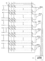
<2.共通電極の構成>
次に、図1および図3を参照しつつ、本実施形態における共通電極14の構成について説明する。図3は、本実施形態における共通電極14の構成を示す概略図である。図3に示すように、CFガラス基板16上において、共通電極14はk個に分割されている。それら分割された共通電極14(1)〜14(k)はそれぞれ共通電極駆動回路24と接続されている。そして、それらの共通電極14(1)〜14(k)にはそれぞれ共通電極駆動信号が与えられる。なお、以下において、k個に分割された共通電極14(1)〜14(k)のうち図3において上からi番目の共通電極のことを「第iの共通電極14(i)」と言い、当該i番目の共通電極に与えられる共通電極駆動信号のことを「第iの共通電極駆動信号COM(i)」と言う。すなわち、第1の共通電極14(1)には第1の共通電極駆動信号COM(1)が、第2の共通電極14(2)には第2の共通電極駆動信号COM(2)が、・・・、第kの共通電極14(k)には第kの共通電極駆動信号COM(k)が、共通電極駆動回路24によってそれぞれ与えられる。以上のように、共通電極14(1)〜14(k)は、共通電極駆動回路24によってそれぞれ独立して駆動される。
<2. Configuration of common electrode>
Next, the configuration of the
図1は、走査信号線と共通電極との関係を示す概略図である。本実施形態においては、図1に示すように、各共通電極はそれぞれ4本の走査信号線と対応付けられるように設けられている。例えば320本の走査信号線GL1〜GL320を備える液晶表示装置の場合、1〜4本目の走査信号線GL1〜GL4に対応して第1の共通電極14(1)が設けられ、5〜8本目の走査信号線GL5〜GL8に対応して第2の共通電極14(2)が設けられ、・・・、317〜320本目の走査信号線GL317〜GL320に対応して第80の共通電極14(80)が設けられている。 FIG. 1 is a schematic diagram showing the relationship between scanning signal lines and common electrodes. In the present embodiment, as shown in FIG. 1, each common electrode is provided so as to be associated with four scanning signal lines. For example, in the case of a liquid crystal display device including 320 scanning signal lines GL1 to GL320, the first common electrode 14 (1) is provided corresponding to the first to fourth scanning signal lines GL1 to GL4, and the fifth to eighth lines. The second common electrode 14 (2) is provided corresponding to the scanning signal lines GL5 to GL8, and the 80th common electrode 14 (corresponding to the 317th to 320th scanning signal lines GL317 to GL320). 80).
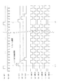
<3.駆動方法>
次に、本実施形態における駆動方法について説明する。図4は、本実施形態における駆動方法を説明するための信号波形図である。走査信号線駆動回路300は、図4(b)に示すゲートクロック信号GCKがハイレベルとなるタイミングで、図4(a)に示すゲートスタートパルス信号GSPを取り込む。そして、ゲートクロック信号GCKがハイレベルからローレベルに変化するタイミングで、ゲートスタートパルス信号GSPに含まれるパルスが、走査信号線駆動回路300内に設けられているシフトレジスタの入力端から出力端へと順次に転送される。これに応じて、図4(c)〜(e)に示すように、走査信号線駆動回路300内のシフトレジスタの各段から順次にアクティブな走査信号が出力される。
<3. Driving method>
Next, a driving method in the present embodiment will be described. FIG. 4 is a signal waveform diagram for explaining the driving method in the present embodiment. The scanning signal
上述したように第1〜第kの共通電極14(1)〜14(k)には第1〜第kの共通電極駆動信号COM(1)〜COM(k)が与えられるところ、図4(f)〜(i)に示すように、1フレーム期間内において各共通電極駆動信号の極性は1水平走査期間毎に反転している。 As described above, the first to kth common electrodes 14 (1) to 14 (k) are supplied with the first to kth common electrode drive signals COM (1) to COM (k). As shown in f) to (i), the polarity of each common electrode drive signal is inverted every horizontal scanning period within one frame period.
図4において、時点t11から時点t12までの期間には、1〜4本目の走査信号線GL1〜GL4に1水平走査期間ずつ順次にアクティブな走査信号G(1)〜G(4)が印加される。この期間中、1〜4本目の走査信号線GL1〜GL4に対応して設けられている第1の共通電極14(1)に与えられる第1の共通電極駆動信号COM(1)の(1水平走査期間毎の)極性は「負、正、負、正」となっている。また、時点t11から時点t12までの期間における第2の共通電極駆動信号COM(2)の(1水平走査期間毎の)極性は「正、負、正、負」となっている。 In FIG. 4, during a period from time t11 to time t12, active scanning signals G (1) to G (4) are sequentially applied to the first to fourth scanning signal lines GL1 to GL4 for each horizontal scanning period. The During this period, (1 horizontal) of the first common electrode drive signal COM (1) applied to the first common electrode 14 (1) provided corresponding to the first to fourth scanning signal lines GL1 to GL4. The polarity (for each scanning period) is “negative, positive, negative, positive”. Further, the polarity (for each horizontal scanning period) of the second common electrode drive signal COM (2) in the period from the time point t11 to the time point t12 is “positive, negative, positive, negative”.
図4において、時点t12から時点t13までの期間には、5〜8本目の走査信号線GL5〜GL8に1水平走査期間ずつ順次にアクティブな走査信号G(5)〜G(8)が印加される。この期間中、5〜8本目の走査信号線GL5〜GL8に対応して設けられている第2の共通電極14(2)に与えられる第2の共通電極駆動信号COM(2)の(1水平走査期間毎の)極性は「正、負、正、負」となっている。また、時点t12から時点t13までの期間における第1の共通電極駆動信号COM(1)の(1水平走査期間毎の)極性は「負、正、負、正」となっている。 In FIG. 4, during the period from time t12 to time t13, the active scanning signals G (5) to G (8) are sequentially applied to the fifth to eighth scanning signal lines GL5 to GL8 by one horizontal scanning period. The During this period, the second common electrode drive signal COM (2) (1 horizontal) applied to the second common electrode 14 (2) provided corresponding to the fifth to eighth scanning signal lines GL5 to GL8. The polarity (for each scanning period) is “positive, negative, positive, negative”. Further, the polarity (for each horizontal scanning period) of the first common electrode drive signal COM (1) in the period from the time point t12 to the time point t13 is “negative, positive, negative, positive”.
図4において、時点t13から次のフレーム期間が開始する時点t21までの期間には、時点t11から時点t13までの期間と同様の動作が繰り返される。そして、次のフレーム期間(時点t21)になると、第1〜第kの共通電極駆動信号COM(1)〜COM(k)についての1水平走査期間毎に現れる極性は、時点t11から時点t21までのフレーム期間における極性とは逆になる。例えば、時点t11から始まるフレーム期間における第1の共通電極駆動信号COM(1)の(1水平走査期間毎の)極性は「負、正、負、正」となっているが、時点t21から始まるフレーム期間における第1の共通電極駆動信号COM(1)の(1水平走査期間毎の)極性は「正、負、正、負」となっている。 In FIG. 4, in the period from time t13 to time t21 when the next frame period starts, the same operation as in the period from time t11 to time t13 is repeated. In the next frame period (time t21), the polarities appearing in each horizontal scanning period for the first to k-th common electrode drive signals COM (1) to COM (k) are from time t11 to time t21. This is opposite to the polarity in the frame period. For example, the polarity (for each horizontal scanning period) of the first common electrode drive signal COM (1) in the frame period starting from time t11 is “negative, positive, negative, positive”, but starts from time t21. The polarity (for each horizontal scanning period) of the first common electrode drive signal COM (1) in the frame period is “positive, negative, positive, negative”.
ここで、図4(f)、(g)に着目すると、各時点において、第1の共通電極駆動信号COM(1)の極性と第2の共通電極駆動信号COM(2)の極性とは互いに逆になっている。また、図4(h)、(i)に着目すると、各時点において、第3の共通電極駆動信号COM(3)の極性と第4の共通電極駆動信号COM(4)の極性とは互いに逆になっている。このように、本実施形態においては、第j(jは奇数)の共通電極14(j)と第(j+1)の共通電極14(j+1)とが対になっており、その一対の共通電極の一方と他方とには、各時点においてそれぞれ異なる極性の共通電極駆動信号が与えられる。 Here, focusing on FIGS. 4F and 4G, the polarity of the first common electrode drive signal COM (1) and the polarity of the second common electrode drive signal COM (2) are mutually different at each time point. It is reversed. 4 (h) and 4 (i), the polarity of the third common electrode drive signal COM (3) and the polarity of the fourth common electrode drive signal COM (4) are opposite to each other at each time point. It has become. As described above, in this embodiment, the j-th (j is an odd number) common electrode 14 (j) and the (j + 1) -th common electrode 14 (j + 1) are paired. One and the other are supplied with common electrode drive signals having different polarities at each time point.
<4.効果>
以上のように、本実施形態によると、液晶層13を介して各画素形成部の画素電極12との間に電圧を印加するための共通電極14はk個に分割されている。そして、そのk個に分割された第1〜第kの共通電極14(1)〜14(k)はそれぞれ独立して共通電極駆動回路24によって駆動され、一対の共通電極を構成する互いに隣接する2つの共通電極のそれぞれには、互いに逆の極性となる共通電極駆動信号が与えられる。このため、隣接する共通電極間において、共通電極電位の極性反転に起因して生じる電気的な振動が互いに打ち消される。これにより、共通電極電位の極性反転に起因する音鳴りの発生が抑制される。また、本実施形態によると、制振材などの部材を備える必要がないのでコストの上昇を抑制することができる。
<4. Effect>
As described above, according to the present embodiment, the
<5.変形例>
以下、上記実施形態の変形例について説明する。
<5. Modification>
Hereinafter, modifications of the embodiment will be described.
<5.1 第1の変形例>
上記実施形態においては、4本の走査信号線毎に1つの共通電極が設けられている例を挙げて説明したが、本発明はこれに限定されない。共通電極の分割数は特に限定されることなく、例えば図5に示すように、共通電極が4個のみに分割されている構成すなわち320本の走査信号線を備えている場合に80本の走査信号線毎に1つの共通電極が設けられる構成であっても良い。但し、より細かく共通電極を分割する方が、各共通電極で生じる電気的振動が小さくなるので、より音鳴りの発生を抑制する効果が得られる。従って、コストと音鳴り抑制の効果とのバランスを考慮しつつ、共通電極の分割数が決定されることが好ましい。
<5.1 First Modification>
In the above embodiment, an example in which one common electrode is provided for every four scanning signal lines has been described, but the present invention is not limited to this. The number of divisions of the common electrode is not particularly limited. For example, as shown in FIG. 5, when the common electrode is divided into only four pieces, that is, when 320 scanning signal lines are provided, 80 scans are performed. The configuration may be such that one common electrode is provided for each signal line. However, if the common electrode is divided more finely, the electric vibration generated in each common electrode is reduced, so that the effect of suppressing the generation of noise can be obtained. Therefore, it is preferable that the number of divisions of the common electrode is determined in consideration of the balance between the cost and the noise reduction effect.
<5.2 第2の変形例>
上記実施形態においては、図4に示したように、互いに隣接する2つの共通電極に与えられる共通電極駆動信号の極性は、いずれの組み合わせに係る2つの共通電極についても互いに逆の極性となっている。すなわち、上記実施形態においては、表示部100内で順次に配置されている共通電極14(1)〜14(k)には、交互に、異なる極性の共通電極駆動信号が与えられていた。しかしながら、本発明はこれに限定されない。例えば、図6に示すように、第1の共通電極駆動信号COM(1)と第4の共通電極駆動信号COM(4)とが同極性で、かつ、それらの信号COM(1)、COM(4)と第2の共通電極駆動信号COM(2)、第3の共通電極駆動信号COM(3)とが逆極性となっていても良い。また、図7に示すように、第1の共通電極駆動信号COM(1)と第2の共通電極駆動信号COM(2)とが同極性で、かつ、それらの信号COM(1)、COM(2)と第3の共通電極駆動信号COM(3)、第4の共通電極駆動信号COM(4)とが逆極性となっていても良い。
<5.2 Second Modification>
In the above embodiment, as shown in FIG. 4, the polarities of the common electrode driving signals given to the two common electrodes adjacent to each other are opposite to each other for the two common electrodes according to any combination. Yes. That is, in the above embodiment, the common electrodes 14 (1) to 14 (k) sequentially arranged in the
<5.3 第3の変形例>
上記実施形態においては、各共通電極には同じ本数の走査信号線が対応付けられるように共通電極の分割が行われていたが、本発明はこれに限定されず、共通電極毎に対応付けられる走査信号線の本数が異なっていても良い。例えば、図8に示すように、「第1の共通電極14(1)には20本の走査信号線GL1〜GL20が対応付けられ、第2の共通電極14(2)には80本の走査信号線GL21〜GL100が対応付けられ、第3の共通電極14(3)には60本の走査信号線GL101〜GL160が対応付けられている」というような構成であっても良い。この場合、例えば図9に示すように、第1の共通電極駆動信号COM(1)と第3の共通電極駆動信号COM(3)とを同極性とし、それらの信号COM(1)、COM(3)と第2の共通電極駆動信号COM(2)とを逆極性とすることにより、比較的効果的に音鳴りの発生が抑制される。
<5.3 Third Modification>
In the above embodiment, the common electrodes are divided so that the same number of scanning signal lines is associated with each common electrode. However, the present invention is not limited to this, and is associated with each common electrode. The number of scanning signal lines may be different. For example, as shown in FIG. 8, “20 scanning signal lines GL1 to GL20 are associated with the first common electrode 14 (1), and 80 scans are associated with the second common electrode 14 (2). The signal lines GL21 to GL100 are associated with each other, and the 60 scanning signal lines GL101 to GL160 are associated with the third common electrode 14 (3). In this case, for example, as shown in FIG. 9, the first common electrode drive signal COM (1) and the third common electrode drive signal COM (3) have the same polarity, and their signals COM (1), COM ( By making the polarity of 3) and the second common electrode drive signal COM (2) opposite in polarity, the generation of sound is suppressed relatively effectively.
<5.4 第4の変形例>
図10は、上記実施形態の第4の変形例における共通電極の構成を示す概略図である。上記実施形態においては、共通電極はk個に分割され、第1〜第kの共通電極14(1)〜14(k)はそれぞれ独立して駆動されていた。一方、本変形例においては、図10に示すように、CFガラス基板16上に2個の櫛形の共通電極14a、14bが設けられ、それらの櫛歯部が互いに噛み合って対向するように配置されている。それら2個の共通電極14a、14bに関し、例えば、一方の共通電極14aは1〜4本目、9〜12本目、17〜20本目、・・・の走査信号線に対応し、他方の共通電極14bは5〜8本目、13〜16本目、21〜24本目、・・・の走査信号線に対応している。そして、一方の共通電極14aには図4(f)、(h)に示した波形と同様の波形の共通電極駆動信号COMaが与えられ、他方の共通電極14bには図4(g)、(i)に示した波形と同様の波形の共通電極駆動信号COMbが与えられる。
<5.4 Fourth Modification>
FIG. 10 is a schematic diagram showing the configuration of the common electrode in the fourth modification of the embodiment. In the above embodiment, the common electrode is divided into k pieces, and the first to kth common electrodes 14 (1) to 14 (k) are driven independently. On the other hand, in this modified example, as shown in FIG. 10, two comb-shaped
本変形例によれば、共通電極駆動回路24において2種類だけの共通電極駆動信号COMa、COMbが生成されれば良いので、共通電極駆動回路24の内部構成を簡単な構成にすることができる。
According to this modification, only two types of common electrode drive signals COMa and COMb need be generated in the common
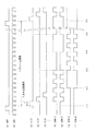
<5.5 第5の変形例>
図11は、上記実施形態の第5の変形例における駆動方法を説明するための信号波形図である。本変形例においては、選択状態の走査信号線に対応して設けられている共通電極を含む一対の共通電極以外の共通電極に与えられる共通電極駆動信号の極性の変化する周期が、当該選択状態の走査信号線に対応して設けられている共通電極を含む一対の共通電極に与えられる共通電極駆動信号の極性の変化する周期よりも長くなるように、第1〜第kの共通電極14(1)〜14(k)のそれぞれに第1〜第kの共通電極駆動信号COM(1)〜COM(k)が与えられる。
<5.5 Fifth Modification>
FIG. 11 is a signal waveform diagram for explaining a driving method in the fifth modification of the embodiment. In this modification, the cycle in which the polarity of the common electrode drive signal applied to the common electrode other than the pair of common electrodes including the common electrode provided corresponding to the scanning signal line in the selected state is the selected state. The first to k-th common electrodes 14 (so as to be longer than the period in which the polarity of the common electrode drive signal applied to the pair of common electrodes including the common electrode provided corresponding to the scanning signal line is changed. The first to kth common electrode drive signals COM (1) to COM (k) are given to 1) to 14 (k), respectively.
例えば、図11において、時点t11から時点t12までの期間には、1〜4本目の走査信号線GL1〜GL4に1水平走査期間ずつ順次にアクティブな走査信号G(1)〜G(4)が印加される。この期間中、1〜4本目の走査信号線GL1〜GL4に対応して設けられている第1の共通電極14(1)に与えられる第1の共通電極駆動信号COM(1)と、当該第1の共通電極14(1)と対になっている第2の共通電極14(2)に与えられる第2の共通電極駆動信号COM(2)とについては、1水平走査期間毎に極性が変化する。一方、第1および第2の共通電極14(1)、(2)以外の共通電極に与えられる共通電極駆動信号については、極性は変化しない。 For example, in FIG. 11, during the period from time t11 to time t12, active scanning signals G (1) to G (4) are sequentially applied to the first to fourth scanning signal lines GL1 to GL4 by one horizontal scanning period. Applied. During this period, the first common electrode drive signal COM (1) applied to the first common electrode 14 (1) provided corresponding to the first to fourth scanning signal lines GL1 to GL4, and the first The polarity of the second common electrode drive signal COM (2) given to the second common electrode 14 (2) paired with one common electrode 14 (1) changes every horizontal scanning period. To do. On the other hand, the polarity does not change for the common electrode drive signal applied to the common electrodes other than the first and second common electrodes 14 (1) and (2).
また、時点t12から時点t13までの期間には、5〜8本目の走査信号線GL5〜GL8に1水平走査期間ずつ順次にアクティブな走査信号G(5)〜G(8)が印加される。この期間中、5〜8本目の走査信号線GL5〜GL8に対応して設けられている第2の共通電極14(2)に与えられる第2の共通電極駆動信号COM(2)と、当該第2の共通電極14(2)と対になっている第1の共通電極14(1)に与えられる第1の共通電極駆動信号COM(1)とについては、1水平走査期間毎に極性が変化する。一方、第1および第2の共通電極14(1)、(2)以外の共通電極に与えられる共通電極駆動信号については、極性は変化しない。 In the period from time t12 to time t13, the active scanning signals G (5) to G (8) are sequentially applied to the fifth to eighth scanning signal lines GL5 to GL8 by one horizontal scanning period. During this period, the second common electrode drive signal COM (2) applied to the second common electrode 14 (2) provided corresponding to the fifth to eighth scanning signal lines GL5 to GL8, and the second The polarity of the first common electrode drive signal COM (1) applied to the first common electrode 14 (1) paired with the two common electrodes 14 (2) changes every horizontal scanning period. To do. On the other hand, the polarity does not change for the common electrode drive signal applied to the common electrodes other than the first and second common electrodes 14 (1) and (2).
さらに、時点t13から時点t14までの期間には、9〜12本目の走査信号線GL9〜GL12に1水平走査期間ずつ順次にアクティブな走査信号G(9)〜G(12)が印加される。この期間中、9〜12本目の走査信号線GL9〜GL12に対応して設けられている第3の共通電極14(3)に与えられる第3の共通電極駆動信号COM(3)と、当該第3の共通電極14(3)と対になっている第4の共通電極14(4)に与えられる第4の共通電極駆動信号COM(4)とについては、1水平走査期間毎に極性が変化する。一方、第3および第4の共通電極14(3)、(4)以外の共通電極に与えられる共通電極駆動信号については、極性は変化しない。 Further, during the period from time t13 to time t14, the active scanning signals G (9) to G (12) are sequentially applied to the ninth to twelfth scanning signal lines GL9 to GL12 for each horizontal scanning period. During this period, the third common electrode drive signal COM (3) provided to the third common electrode 14 (3) provided corresponding to the ninth to twelfth scanning signal lines GL9 to GL12, and the first The polarity of the fourth common electrode drive signal COM (4) applied to the fourth common electrode 14 (4) paired with the three common electrodes 14 (3) changes every horizontal scanning period. To do. On the other hand, the polarity does not change for the common electrode drive signal applied to the common electrodes other than the third and fourth common electrodes 14 (3) and (4).
さらにまた、時点t14から時点t15までの期間には、13〜16本目の走査信号線GL13〜GL16に1水平走査期間ずつ順次にアクティブな走査信号G(13)〜G(16)が印加される。この期間中、13〜16本目の走査信号線GL13〜GL16に対応して設けられている第4の共通電極14(4)に与えられる第4の共通電極駆動信号COM(4)と、当該第4の共通電極14(4)と対になっている第3の共通電極14(3)に与えられる第3の共通電極駆動信号COM(3)とについては、1水平走査期間毎に極性が変化する。一方、第3および第4の共通電極14(3)、(4)以外の共通電極に与えられる共通電極駆動信号については、極性は変化しない。 Furthermore, during the period from time t14 to time t15, the active scanning signals G (13) to G (16) are sequentially applied to the 13th to 16th scanning signal lines GL13 to GL16 for each horizontal scanning period. . During this period, the fourth common electrode drive signal COM (4) applied to the fourth common electrode 14 (4) provided corresponding to the 13th to 16th scanning signal lines GL13 to GL16, and the fourth The polarity of the third common electrode drive signal COM (3) given to the third common electrode 14 (3) paired with the four common electrodes 14 (4) changes every horizontal scanning period. To do. On the other hand, the polarity does not change for the common electrode drive signal applied to the common electrodes other than the third and fourth common electrodes 14 (3) and (4).
本変形例によれば、任意の一対の共通電極に着目すると、当該一対の共通電極に対応している走査信号線のうちのいずれかにアクティブな走査信号が印加されている期間中のみ、1水平走査期間毎に反転する共通電極駆動信号が与えられ、それ以外の期間中には共通電極電位反転周波数が低減されている。このため、各共通電極に与えられる共通電極駆動信号の極性が1フレーム期間を通じて1水平走査期間毎に反転する構成と比べて、消費電力が大きく低減される。 According to this modification, when paying attention to an arbitrary pair of common electrodes, only during a period in which an active scanning signal is applied to one of the scanning signal lines corresponding to the pair of common electrodes, A common electrode drive signal that is inverted every horizontal scanning period is given, and the common electrode potential inversion frequency is reduced during other periods. For this reason, the power consumption is greatly reduced as compared with the configuration in which the polarity of the common electrode drive signal applied to each common electrode is inverted every horizontal scanning period through one frame period.
なお、第2の共通電極駆動信号COM(2)と第3の共通電極駆動信号COM(3)とについての共通電極電位反転周波数を低減させることができないような場合、もしくは、第1の共通電極駆動信号COM(1)と第4の共通電極駆動信号COM(4)の表示領域の周波数を他の領域に比べて低減させて駆動させることが可能な場合には、例えば図12に示すように、第1の共通電極駆動信号COM(1)と第4の共通電極駆動信号COM(4)とについての共通電極電位反転周波数を常に低い状態にすることにより消費電力を低減させることができる。 Note that the common electrode potential inversion frequency for the second common electrode drive signal COM (2) and the third common electrode drive signal COM (3) cannot be reduced, or the first common electrode In the case where the drive signal COM (1) and the fourth common electrode drive signal COM (4) can be driven with the frequency of the display area reduced as compared with other areas, for example, as shown in FIG. The power consumption can be reduced by always setting the common electrode potential inversion frequency for the first common electrode drive signal COM (1) and the fourth common electrode drive signal COM (4) to a low state.
<5.6 第6の変形例>
上記実施形態においては、k個の極性反転信号POL(1)〜POL(k)に基づいてk個の共通電極駆動信号COM(1)〜COM(k)が生成されていたが、本発明はこれに限定されない。図4に示すように、奇数番目の共通電極に与えられる共通電極駆動信号の波形は全て同じ波形となっており、偶数番目の共通電極に与えられる共通電極駆動信号の波形についても全て同じ波形となっている。また、奇数番目の共通電極に与えられる共通電極駆動信号と偶数番目の共通電極に与えられる共通電極駆動信号とは、極性の反転するタイミングが同じである。従って、例えば図13に示すように、奇数番目の共通電極に与えられる共通電極駆動信号を生成する第1駆動部246と偶数番目の共通電極に与えられる共通電極駆動信号を生成する第2駆動部247とを備え、第1駆動部246には極性反転信号POLをそのまま与え、第2駆動部247にはインバータ245によって極性反転信号POLの極性を反転させた信号を与える構成とすることもできる。これにより、コントロール回路21から共通電極駆動回路24に与えるべき極性反転信号POLの数が削減されるとともに、共通電極駆動回路24の内部構成が簡単になる。
<5.6 Sixth Modification>
In the above embodiment, k common electrode drive signals COM (1) to COM (k) are generated based on the k polarity inversion signals POL (1) to POL (k). It is not limited to this. As shown in FIG. 4, the waveforms of the common electrode drive signals given to the odd-numbered common electrodes are all the same waveform, and the waveforms of the common electrode drive signals given to the even-numbered common electrodes are all the same waveform. It has become. Further, the common electrode drive signal given to the odd-numbered common electrode and the common electrode drive signal given to the even-numbered common electrode have the same timing of polarity inversion. Therefore, for example, as shown in FIG. 13, the
12…画素電極
13…液晶層
14(1)〜(k)…共通電極
15…TFTガラス基板
16…CFガラス基板
21…コントロール回路
24…共通電極駆動回路
100…表示部
200…表示制御回路
300…走査信号線駆動回路(ゲートドライバ)
400…映像信号線駆動回路(ソースドライバ)
COM(1)〜(k)…共通電極駆動信号
GL1〜GLm…走査信号線(ゲートバスライン)
POL(1)〜(k)…極性反転信号
SL1〜SLn…映像信号線(ソースバスライン)
DESCRIPTION OF
400 ... Video signal line drive circuit (source driver)
COM (1) to (k) ... Common electrode drive signals GL1 to GLm ... Scanning signal lines (gate bus lines)
POL (1) to (k): polarity inversion signals SL1 to SLn: video signal lines (source bus lines)
Claims (10)
前記複数の画素電極との間に電圧を印加するために、それぞれが1以上の走査信号線と対応するように設けられた複数の共通電極と、
所定の電圧レベルを基準として正極性の電圧と負極性の電圧とを共通電極駆動信号として前記複数の共通電極のそれぞれに与えるための共通電極駆動回路と
を備え、
前記共通電極駆動回路は、各共通電極に正極性の電圧と負極性の電圧とが交互に与えられることに起因して生ずる電気的な振動が互いに打ち消されるように、各共通電極に与えられる共通電極駆動信号の極性を変化させることを特徴とする、液晶表示装置。 A plurality of video signal lines for respectively transmitting a plurality of video signals representing an image to be displayed, a plurality of scanning signal lines intersecting with the plurality of video signal lines, the plurality of video signal lines and the plurality of scannings A plurality of pixel electrodes provided in a plurality of pixel formation portions arranged in a matrix corresponding to intersections with the signal lines, and a video signal line drive for supplying the plurality of video signals to the plurality of video signal lines An active matrix liquid crystal display device comprising a circuit and a scanning signal line driving circuit for selectively driving the plurality of scanning signal lines,
A plurality of common electrodes provided so as to correspond to one or more scanning signal lines in order to apply a voltage between the plurality of pixel electrodes;
A common electrode drive circuit for applying a positive voltage and a negative voltage to each of the plurality of common electrodes as a common electrode drive signal with a predetermined voltage level as a reference,
The common electrode driving circuit has a common voltage applied to each common electrode such that electrical vibrations caused by alternately applying a positive voltage and a negative voltage to each common electrode cancel each other. A liquid crystal display device characterized by changing the polarity of an electrode drive signal.
前記共通電極駆動回路は、一対の共通電極の一方と他方とにそれぞれ異なる極性の電圧が与えられるように、前記複数の共通電極のそれぞれに前記共通電極駆動信号を与えることを特徴とする、請求項1に記載の液晶表示装置。 Each common electrode is paired with one of the other common electrodes arranged adjacent to it,
The common electrode driving circuit provides the common electrode driving signal to each of the plurality of common electrodes so that voltages having different polarities are applied to one and the other of the pair of common electrodes, respectively. Item 2. A liquid crystal display device according to item 1.
前記複数の映像信号を前記複数の映像信号線に供給する映像信号線駆動回路と、
前記複数の走査信号線を選択的に駆動する走査信号線駆動回路と、
所定の電圧レベルを基準として正極性の電圧と負極性の電圧とを共通電極駆動信号として前記複数の共通電極のそれぞれに与えるための共通電極駆動回路と
を備え、
前記共通電極駆動回路は、各共通電極に正極性の電圧と負極性の電圧とが交互に与えられることに起因して生ずる電気的な振動が互いに打ち消されるように、各共通電極に与えられる共通電極駆動信号の極性を変化させることを特徴とする、駆動回路。 A plurality of video signal lines for respectively transmitting a plurality of video signals representing an image to be displayed, a plurality of scanning signal lines intersecting with the plurality of video signal lines, the plurality of video signal lines and the plurality of scannings In order to apply a voltage between the plurality of pixel electrodes provided in the plurality of pixel formation portions arranged in a matrix corresponding to the intersections with the signal lines and the plurality of pixel electrodes, respectively. A drive circuit of an active matrix type liquid crystal display device comprising a plurality of common electrodes provided to correspond to the scanning signal lines,
A video signal line driving circuit for supplying the plurality of video signals to the plurality of video signal lines;
A scanning signal line driving circuit for selectively driving the plurality of scanning signal lines;
A common electrode drive circuit for applying a positive voltage and a negative voltage to each of the plurality of common electrodes as a common electrode drive signal with a predetermined voltage level as a reference,
The common electrode driving circuit has a common voltage applied to each common electrode such that electrical vibrations caused by alternately applying a positive voltage and a negative voltage to each common electrode cancel each other. A drive circuit, wherein the polarity of an electrode drive signal is changed.
前記複数の映像信号を前記複数の映像信号線に供給する映像信号線駆動ステップと、
前記複数の走査信号線を選択的に駆動する走査信号線駆動ステップと、
所定の電圧レベルを基準として正極性の電圧と負極性の電圧とを共通電極駆動信号として前記複数の共通電極のそれぞれに与えるための共通電極駆動ステップと
を備え、
前記共通電極駆動ステップでは、各共通電極に正極性の電圧と負極性の電圧とが交互に与えられることに起因して生ずる電気的な振動が互いに打ち消されるように、各共通電極に与えられる共通電極駆動信号の極性が変化することを特徴とする、駆動方法。 A plurality of video signal lines for respectively transmitting a plurality of video signals representing an image to be displayed, a plurality of scanning signal lines intersecting with the plurality of video signal lines, the plurality of video signal lines and the plurality of scannings In order to apply a voltage between the plurality of pixel electrodes provided in the plurality of pixel formation portions arranged in a matrix corresponding to the intersections with the signal lines and the plurality of pixel electrodes, respectively. A driving method of an active matrix type liquid crystal display device comprising a plurality of common electrodes provided so as to correspond to the scanning signal lines,
A video signal line driving step of supplying the plurality of video signals to the plurality of video signal lines;
A scanning signal line driving step of selectively driving the plurality of scanning signal lines;
A common electrode driving step for applying a positive voltage and a negative voltage to each of the plurality of common electrodes as a common electrode drive signal with a predetermined voltage level as a reference,
In the common electrode driving step, a common voltage applied to each common electrode is canceled so that electrical vibrations caused by alternately applying a positive voltage and a negative voltage to each common electrode are canceled. A driving method characterized in that the polarity of an electrode driving signal changes.
Priority Applications (1)
| Application Number | Priority Date | Filing Date | Title |
|---|---|---|---|
| JP2007169868A JP2009008869A (en) | 2007-06-28 | 2007-06-28 | Liquid crystal display device, driving circuit and driving method thereof |
Applications Claiming Priority (1)
| Application Number | Priority Date | Filing Date | Title |
|---|---|---|---|
| JP2007169868A JP2009008869A (en) | 2007-06-28 | 2007-06-28 | Liquid crystal display device, driving circuit and driving method thereof |
Publications (1)
| Publication Number | Publication Date |
|---|---|
| JP2009008869A true JP2009008869A (en) | 2009-01-15 |
Family
ID=40324016
Family Applications (1)
| Application Number | Title | Priority Date | Filing Date |
|---|---|---|---|
| JP2007169868A Pending JP2009008869A (en) | 2007-06-28 | 2007-06-28 | Liquid crystal display device, driving circuit and driving method thereof |
Country Status (1)
| Country | Link |
|---|---|
| JP (1) | JP2009008869A (en) |
Cited By (3)
| Publication number | Priority date | Publication date | Assignee | Title |
|---|---|---|---|---|
| JP2009075489A (en) * | 2007-09-25 | 2009-04-09 | Casio Comput Co Ltd | Active matrix display device |
| CN103197456A (en) * | 2013-04-24 | 2013-07-10 | 深圳市华星光电技术有限公司 | Liquid crystal display as well as method for improving horizontal black belt of liquid crystal display and drive circuit |
| CN105374334A (en) * | 2015-12-11 | 2016-03-02 | 武汉华星光电技术有限公司 | Liquid crystal display panel structure |
-
2007
- 2007-06-28 JP JP2007169868A patent/JP2009008869A/en active Pending
Cited By (4)
| Publication number | Priority date | Publication date | Assignee | Title |
|---|---|---|---|---|
| JP2009075489A (en) * | 2007-09-25 | 2009-04-09 | Casio Comput Co Ltd | Active matrix display device |
| CN103197456A (en) * | 2013-04-24 | 2013-07-10 | 深圳市华星光电技术有限公司 | Liquid crystal display as well as method for improving horizontal black belt of liquid crystal display and drive circuit |
| CN105374334A (en) * | 2015-12-11 | 2016-03-02 | 武汉华星光电技术有限公司 | Liquid crystal display panel structure |
| CN105374334B (en) * | 2015-12-11 | 2018-06-01 | 武汉华星光电技术有限公司 | Structure of liquid crystal display panel |
Similar Documents
| Publication | Publication Date | Title |
|---|---|---|
| US9548031B2 (en) | Display device capable of driving at low speed | |
| US9978323B2 (en) | Liquid crystal display panel and display device | |
| CN101196629B (en) | Liquid crystal display device and driving method thereof | |
| CN100535715C (en) | Liquid crystal display device and driving method | |
| JP5426167B2 (en) | Display device | |
| JP5955098B2 (en) | Liquid crystal display device, data line driving circuit, and liquid crystal display device driving method | |
| CN104134418A (en) | Display device for low speed drive and method for driving the same | |
| TW201241810A (en) | Liquid crystal display | |
| JP2007094404A (en) | Liquid crystal display device and driving method thereof | |
| WO2010113359A1 (en) | Liquid crystal display apparatus, drive circuit therefor, and drive method therefor | |
| JP2009008869A (en) | Liquid crystal display device, driving circuit and driving method thereof | |
| JP2006072211A (en) | Liquid crystal display device and driving method of liquid crystal display device | |
| JP4270442B2 (en) | Display device and driving method thereof | |
| JP2007334283A (en) | Liquid crystal display device and driving method thereof | |
| KR101818248B1 (en) | Liquid crystal display | |
| WO2013031552A1 (en) | Liquid-crystal display device and method for driving same | |
| KR101174783B1 (en) | Apparatus and method for driving of liquid crystal display device | |
| KR20140081555A (en) | Liquid crystal display and method of driving the same | |
| KR101166829B1 (en) | Apparatus and method for driving of liquid crystal display device | |
| KR20110043892A (en) | LCD and its driving method | |
| JP2006023576A (en) | Liquid crystal display | |
| CN100535979C (en) | Liquid crystal panel and liquid crystal display device having the same | |
| JP4622398B2 (en) | Liquid crystal display device and driving method of liquid crystal display device | |
| KR100994229B1 (en) | LCD and its driving method | |
| JP4781884B2 (en) | Liquid crystal display panel and liquid crystal display device including the same |