JP2008172082A - Semiconductor device and manufacturing method of semiconductor device - Google Patents
Semiconductor device and manufacturing method of semiconductor device Download PDFInfo
- Publication number
- JP2008172082A JP2008172082A JP2007004672A JP2007004672A JP2008172082A JP 2008172082 A JP2008172082 A JP 2008172082A JP 2007004672 A JP2007004672 A JP 2007004672A JP 2007004672 A JP2007004672 A JP 2007004672A JP 2008172082 A JP2008172082 A JP 2008172082A
- Authority
- JP
- Japan
- Prior art keywords
- insulating film
- fin
- forming
- line
- region
- Prior art date
- Legal status (The legal status is an assumption and is not a legal conclusion. Google has not performed a legal analysis and makes no representation as to the accuracy of the status listed.)
- Pending
Links
Images


Classifications
-
- H—ELECTRICITY
- H10—SEMICONDUCTOR DEVICES; ELECTRIC SOLID-STATE DEVICES NOT OTHERWISE PROVIDED FOR
- H10D—INORGANIC ELECTRIC SEMICONDUCTOR DEVICES
- H10D30/00—Field-effect transistors [FET]
- H10D30/60—Insulated-gate field-effect transistors [IGFET]
- H10D30/62—Fin field-effect transistors [FinFET]
-
- H—ELECTRICITY
- H10—SEMICONDUCTOR DEVICES; ELECTRIC SOLID-STATE DEVICES NOT OTHERWISE PROVIDED FOR
- H10D—INORGANIC ELECTRIC SEMICONDUCTOR DEVICES
- H10D30/00—Field-effect transistors [FET]
- H10D30/01—Manufacture or treatment
- H10D30/021—Manufacture or treatment of FETs having insulated gates [IGFET]
- H10D30/024—Manufacture or treatment of FETs having insulated gates [IGFET] of fin field-effect transistors [FinFET]
-
- H—ELECTRICITY
- H10—SEMICONDUCTOR DEVICES; ELECTRIC SOLID-STATE DEVICES NOT OTHERWISE PROVIDED FOR
- H10D—INORGANIC ELECTRIC SEMICONDUCTOR DEVICES
- H10D30/00—Field-effect transistors [FET]
- H10D30/60—Insulated-gate field-effect transistors [IGFET]
- H10D30/62—Fin field-effect transistors [FinFET]
- H10D30/6212—Fin field-effect transistors [FinFET] having fin-shaped semiconductor bodies having non-rectangular cross-sections
- H10D30/6213—Fin field-effect transistors [FinFET] having fin-shaped semiconductor bodies having non-rectangular cross-sections having rounded corners
-
- H—ELECTRICITY
- H10—SEMICONDUCTOR DEVICES; ELECTRIC SOLID-STATE DEVICES NOT OTHERWISE PROVIDED FOR
- H10D—INORGANIC ELECTRIC SEMICONDUCTOR DEVICES
- H10D30/00—Field-effect transistors [FET]
- H10D30/60—Insulated-gate field-effect transistors [IGFET]
- H10D30/67—Thin-film transistors [TFT]
- H10D30/6729—Thin-film transistors [TFT] characterised by the electrodes
- H10D30/673—Thin-film transistors [TFT] characterised by the electrodes characterised by the shapes, relative sizes or dispositions of the gate electrodes
- H10D30/6735—Thin-film transistors [TFT] characterised by the electrodes characterised by the shapes, relative sizes or dispositions of the gate electrodes having gates fully surrounding the channels, e.g. gate-all-around
-
- H—ELECTRICITY
- H10—SEMICONDUCTOR DEVICES; ELECTRIC SOLID-STATE DEVICES NOT OTHERWISE PROVIDED FOR
- H10D—INORGANIC ELECTRIC SEMICONDUCTOR DEVICES
- H10D62/00—Semiconductor bodies, or regions thereof, of devices having potential barriers
- H10D62/10—Shapes, relative sizes or dispositions of the regions of the semiconductor bodies; Shapes of the semiconductor bodies
- H10D62/117—Shapes of semiconductor bodies
- H10D62/118—Nanostructure semiconductor bodies
- H10D62/119—Nanowire, nanosheet or nanotube semiconductor bodies
- H10D62/121—Nanowire, nanosheet or nanotube semiconductor bodies oriented parallel to substrates
-
- H—ELECTRICITY
- H10—SEMICONDUCTOR DEVICES; ELECTRIC SOLID-STATE DEVICES NOT OTHERWISE PROVIDED FOR
- H10D—INORGANIC ELECTRIC SEMICONDUCTOR DEVICES
- H10D30/00—Field-effect transistors [FET]
- H10D30/60—Insulated-gate field-effect transistors [IGFET]
- H10D30/67—Thin-film transistors [TFT]
- H10D30/6704—Thin-film transistors [TFT] having supplementary regions or layers in the thin films or in the insulated bulk substrates for controlling properties of the device
- H10D30/6727—Thin-film transistors [TFT] having supplementary regions or layers in the thin films or in the insulated bulk substrates for controlling properties of the device having source or drain regions connected to bulk conducting substrates
Landscapes
- Insulated Gate Type Field-Effect Transistor (AREA)
- Electrodes Of Semiconductors (AREA)
- Element Separation (AREA)
- Internal Circuitry In Semiconductor Integrated Circuit Devices (AREA)
- Metal-Oxide And Bipolar Metal-Oxide Semiconductor Integrated Circuits (AREA)
- Thin Film Transistor (AREA)
Abstract
【課題】簡便かつ低コストにプレーナ領域と混載することが可能なフィン型電界効果トランジスタを含んだ半導体装置の製造方法を提供すること。
【解決手段】半導体装置の製造方法は、基板10の主表面にライン状の絶縁膜を形成し、絶縁膜をマスクに基板をエッチングして絶縁膜の両側に第1の溝を形成し、第1の溝それぞれの側壁に側壁絶縁膜を形成し、絶縁膜及び側壁絶縁膜をマスクに基板をエッチングして第1の溝の底部それぞれに第2の溝を形成し、絶縁膜及び側壁絶縁膜を耐酸化性マスクとして基板を酸化して第2の溝の基板を挟んで隣接する側壁それぞれに形成される酸化領域16を互いに接触させ、絶縁膜及び側壁絶縁膜を除去し、除去によって露出した基板の半導体領域18の表面にゲート絶縁膜21を、その上にゲート電極24を形成し、半導体領域をライン状のフィンとするフィン型電界効果トランジスタを形成する工程を含む。
【選択図】 図14A method of manufacturing a semiconductor device including a fin-type field effect transistor that can be mounted on a planar region in a simple and low cost manner.
A method of manufacturing a semiconductor device includes forming a line-shaped insulating film on a main surface of a substrate, etching the substrate using the insulating film as a mask to form first grooves on both sides of the insulating film, A sidewall insulating film is formed on each sidewall of the first groove, and the substrate is etched using the insulating film and the sidewall insulating film as a mask to form a second groove at each bottom of the first groove. The insulating film and the sidewall insulating film The oxidation region 16 formed on each of the adjacent sidewalls with the substrate of the second groove sandwiched between the substrates using the oxidation-resistant mask as a mask, and the insulating film and the sidewall insulating film are removed and exposed by removal. This includes a step of forming a gate insulating film 21 on the surface of the semiconductor region 18 of the substrate and a gate electrode 24 thereon to form a fin field effect transistor having the semiconductor region as a line-shaped fin.
[Selection] FIG.
Description
本発明は、フィン型FET(電界効果トランジスタ)を含んだ半導体装置およびその製造方法に関する。 The present invention relates to a semiconductor device including a fin-type FET (field effect transistor) and a manufacturing method thereof.
フィン(Fin)型FET(FinFET)、特にバルク(Bulk)Si基板上に作製されたFinFETは、低コストでカットオフ特性が良好なデバイスであるため、次世代トランジスタ構造として有望視されている(例えば、特許文献1参照)。 Fin-type FETs (FinFETs), in particular FinFETs fabricated on bulk Si substrates, are promising as next-generation transistor structures because they are low-cost devices with good cut-off characteristics ( For example, see Patent Document 1).
しかしながら、マルチ閾値電圧の実現やアナログデバイスに対応するには、プレーナ(planar)デバイスの方が簡単で低コストであるため、実際のLSIでは、従来のプレーナ型MOSFETとフィン型FETを混載することが必要である。そのため、両者を混載する簡単な製造プロセスが求められていた。 However, in order to realize multi-threshold voltages and to cope with analog devices, planar devices are simpler and less expensive, so in actual LSIs, conventional planar MOSFETs and fin-type FETs should be mixed. is required. Therefore, there has been a demand for a simple manufacturing process in which both are mixed.
ところが、プレーナ型MOSFETとフィン型FETを混載すると、ゲートの表面が凸凹となって、微細なゲートを作製するためのリソグラフィを行なうことが困難になったり、フィン領域、プレーナ領域のゲートの加工を同時に行なえない等の問題があった。また、工程数が多くなり製造コストが増加するという問題もあった。
本発明は、簡便かつ低コストにプレーナ領域と混載することが可能なフィン型電界効果トランジスタを含んだ半導体装置及びその製造方法を提供する。 The present invention provides a semiconductor device including a fin-type field effect transistor that can be mixed with a planar region easily and at low cost, and a method for manufacturing the same.
この発明の第1の態様に係る半導体装置の製造方法は、半導体基板の主表面にライン状の絶縁膜を形成する工程と、前記ライン状の絶縁膜をマスクとして前記半導体基板をエッチングすることにより前記ライン状の絶縁膜の両側に2つの隣接する第1の溝を形成する工程と、隣接する前記第1の溝それぞれの側壁に側壁絶縁膜を形成する工程と、前記ライン状の絶縁膜及び前記側壁絶縁膜をマスクとして前記半導体基板をエッチングすることにより隣接する前記第1の溝の底部それぞれに第2の溝を形成する工程と、前記ライン状の絶縁膜及び前記側壁絶縁膜を耐酸化性マスクとして前記半導体基板を酸化することにより、前記第2の溝の前記半導体基板を挟んで隣接する側壁それぞれに形成される酸化領域を互いに接触させる工程と、前記ライン状の絶縁膜及び前記側壁絶縁膜を除去する工程と、前記除去によって露出した前記半導体基板の半導体領域の表面にゲート絶縁膜を形成する工程と、前記ゲート絶縁膜の上にゲート電極を形成する工程と、前記半導体領域をライン状のフィンとするフィン型電界効果トランジスタを形成する工程とを含む。 A method of manufacturing a semiconductor device according to a first aspect of the present invention includes a step of forming a line-shaped insulating film on a main surface of a semiconductor substrate, and etching the semiconductor substrate using the line-shaped insulating film as a mask. Forming two adjacent first grooves on both sides of the line-shaped insulating film; forming a sidewall insulating film on each side wall of the adjacent first grooves; and the line-shaped insulating film and Etching the semiconductor substrate using the sidewall insulating film as a mask to form a second groove at each bottom of the adjacent first groove, and oxidizing the line-shaped insulating film and the sidewall insulating film against oxidation Oxidizing the semiconductor substrate as a reactive mask to bring the oxidized regions formed on the side walls adjacent to each other across the semiconductor substrate of the second groove into contact with each other; Removing the in-shaped insulating film and the sidewall insulating film; forming a gate insulating film on a surface of the semiconductor region of the semiconductor substrate exposed by the removal; and forming a gate electrode on the gate insulating film And a step of forming a fin-type field effect transistor having the semiconductor region as a line-shaped fin.
この発明の第2の態様に係る半導体装置の製造方法は、半導体基板の主表面にライン状の第1の絶縁膜と前記第1の絶縁膜より線幅の太い第2の絶縁膜を同時に形成する工程と、
前記第1及び第2の絶縁膜をマスクとして前記半導体基板をエッチングすることにより前記第1及び第2の絶縁膜の両側に複数の第1の溝を形成する工程と、複数の前記第1の溝それぞれの側壁に側壁絶縁膜を形成する工程と、前記第1及び第2の絶縁膜及び前記側壁絶縁膜をマスクとして前記半導体基板をエッチングすることにより複数の前記第1の溝の底部それぞれに第2の溝を形成する工程と、前記第1及び第2の絶縁膜及び前記側壁絶縁膜を耐酸化性マスクとして前記半導体基板を酸化することにより、前記第1の絶縁膜の両側の前記第2の溝の前記半導体基板を挟んで隣接する側壁それぞれに形成される酸化領域を互いに接触させ、前記第2の絶縁膜の両側の前記第2の溝の前記半導体基板を挟んで隣接する側壁それぞれに形成される酸化領域は互いに接触させない工程と、前記第1及び第2の絶縁膜及び前記側壁絶縁膜を除去する工程と、前記第1の絶縁膜の除去によって露出した前記半導体基板の半導体領域の表面にゲート絶縁膜を形成し、前記ゲート絶縁膜の上にゲート電極を形成することにより、前記半導体領域をライン状のフィンとするフィン型電界効果トランジスタを形成する工程と、前記第2の絶縁膜の除去によって露出した前記半導体基板の別の半導体領域にプレーナ型電界効果トランジスタ或いはプレーナ領域を形成する工程とを含む。
According to a second aspect of the present invention, there is provided a method for manufacturing a semiconductor device, wherein a first insulating film having a line shape and a second insulating film having a larger line width than the first insulating film are simultaneously formed on a main surface of a semiconductor substrate. And a process of
Forming a plurality of first trenches on both sides of the first and second insulating films by etching the semiconductor substrate using the first and second insulating films as a mask; Forming a sidewall insulating film on a sidewall of each groove; and etching the semiconductor substrate using the first and second insulating films and the sidewall insulating film as a mask to each of the bottoms of the plurality of first grooves. Forming a second trench; and oxidizing the semiconductor substrate using the first and second insulating films and the sidewall insulating film as an oxidation-resistant mask, thereby forming the first groove on both sides of the first insulating film. The oxide regions formed on the side walls adjacent to each other across the semiconductor substrate in two grooves are brought into contact with each other, and the side walls adjacent to each other across the semiconductor substrate in the second groove on both sides of the second insulating film Formed into An oxide region exposed to the surface of the semiconductor region of the semiconductor substrate exposed by removing the first and second insulating films and the sidewall insulating film, and removing the first insulating film; Forming a gate insulating film, and forming a gate electrode on the gate insulating film, thereby forming a fin-type field effect transistor having the semiconductor region as a line-shaped fin; and Forming a planar field effect transistor or a planar region in another semiconductor region of the semiconductor substrate exposed by the removal.
この発明の第3の態様に係る半導体装置は、バルクシリコン基板の上に形成されたシリコン酸化膜と、前記シリコン酸化膜上に形成されたライン状のフィンと、前記フィンの延伸方向の両端にそれぞれ接続され、前記延伸方向と垂直な方向の幅が前記フィンよりも大きく、上面の高さが前記フィンの上面の高さと一致している前記基板の一部であるプレーナ領域とを具備する。 A semiconductor device according to a third aspect of the present invention includes a silicon oxide film formed on a bulk silicon substrate, line-shaped fins formed on the silicon oxide film, and both ends of the fin in the extending direction. A planar region that is connected to each other and is a part of the substrate having a width in a direction perpendicular to the extending direction larger than that of the fin and a height of an upper surface coinciding with a height of the upper surface of the fin.
本発明によれば、簡便かつ低コストにプレーナ領域と混載することが可能なフィン型電界効果トランジスタを含んだ半導体装置及びその製造方法を提供することができる。 ADVANTAGE OF THE INVENTION According to this invention, the semiconductor device containing the fin type field effect transistor which can be mounted together with a planar area | region simply and at low cost, and its manufacturing method can be provided.
以下、図面を参照して本発明の実施形態について詳細に説明する。 Hereinafter, embodiments of the present invention will be described in detail with reference to the drawings.
図1は以下の実施形態に係るナノワイヤー(nano wire)-フィン型FETの3次元構造を示した図である。幅10nm以下のフィンの高さを低くしてアスペクト比(フィンの高さ/フィンの幅)を1程度に小さくしたMOS(Metal Oxide Semiconductor)FETが、一般に、ナノワイヤー-フィン型FETと呼ばれ、通常、フィン側面だけでなく上面もチャネル面として使用する。特に、チャネルとしてフィンの側面だけでなく、上面と底面も使うようにすると、ゲートオールアラウンド(Gate-all-around)ナノワイヤー-フィン型FETと呼ばれる。 FIG. 1 is a view showing a three-dimensional structure of a nanowire-fin type FET according to the following embodiment. A MOS (Metal Oxide Semiconductor) FET having a low aspect ratio (fin height / fin width) reduced to about 1 by reducing the height of a fin having a width of 10 nm or less is generally called a nanowire-fin type FET. Usually, not only the fin side surface but also the upper surface is used as the channel surface. In particular, if not only the side surface of the fin but also the top and bottom surfaces are used as the channel, it is called a gate-all-around nanowire-fin type FET.
ナノワイヤー-フィン型FETのメリットとしては、(1)通常のフィン型FETよりも短チャネル効果耐性があり、その分、微細化が可能であること、(2)量子閉じ込めによる有効質量と散乱確率の低減の結果、移動度が向上すること、(3)不純物ゆらぎ起因の閾値電圧バラツキが低減すること、等が挙げられる。 Advantages of nanowire-fin type FETs are: (1) Short channel effect resistance compared to normal fin type FETs, miniaturization correspondingly, (2) Effective mass and scattering probability due to quantum confinement As a result of the reduction, the mobility is improved, and (3) the threshold voltage variation due to the impurity fluctuation is reduced.
(第1の実施形態)
本発明の第1の実施形態に係る半導体装置の製造方法を、各製造工程の断面図である図2乃至図14を用いて以下に説明する。
(First embodiment)
A method of manufacturing a semiconductor device according to the first embodiment of the present invention will be described below with reference to FIGS. 2 to 14 which are cross-sectional views of each manufacturing process.
本実施形態においては、図1に示したようなナノワイヤー-フィン型FETをプレーナ型MOSFETと同じ基板上に混載する。 In the present embodiment, a nanowire-fin type FET as shown in FIG. 1 is mounted on the same substrate as the planar MOSFET.
まず図2に示すように、バルクSi基板10の上に厚さ2nm程度の薄い酸化膜(図示せず)を介して、膜厚50nm程度のSiNからなるハードマスク材15を堆積する。ハードマスク材15としては、SiO2、あるいはSiON、更にはSiN/SiO2/SiN等の積層膜、その他の絶縁膜であってもかまわない。
First, as shown in FIG. 2, a
次に、図3に示すように、プレーナ型MOSFET及びナノワイヤー-フィン型FETの活性(チャネル)領域をパターンニングして、それぞれに対するハードマスク11及びハードマスク12、13を形成する。ここで、10nm程度以下の幅のフィンを有するナノワイヤー-フィン型FETを形成するためのライン状のハードマスク12、13の線幅は、プレーナ型MOSFETを形成するためのハードマスク11の線幅よりも小さくしておく。
Next, as shown in FIG. 3, the active (channel) regions of the planar MOSFET and nanowire-fin type FET are patterned to form the
その後、ハードマスク11、12、13をマスクとしてRIE(反応性イオンエッチング)加工を行なうことにより図4に示すように、20nm程度の深さの第1の溝50がバルクSi基板10に形成される。
Thereafter, by performing RIE (reactive ion etching) using the
次に、図5に示すように、この上からSiN膜14を全面に形成した後、図6に示すようにエッチバックすることにより第1の溝50の側面に厚さ20nm程度のSiNの側壁絶縁膜14を形成する。側壁絶縁膜14としては、SiO2、SiON、或いはその他の絶縁膜を用いてもかまわない。
Next, as shown in FIG. 5, an
次いで、図7に示すようにハードマスク11、12、13と側壁絶縁膜14をマスクとしてSi基板10をエッチングして第1の溝50の底部をさらに深く掘って第2の溝60を形成する。
Next, as shown in FIG. 7, the
次に、図8に示すようにハードマスク11、12、13と側壁絶縁膜14を耐酸化性マスクとして第2の溝60の底部に露出したSi基板10の表面を酸化して酸化膜16を形成する。その際、ハードマスク12、13の下のフィンとなるべき領域の下においてその両側の第2の溝60側壁からの酸化膜16が互いに接触するように酸化膜厚を調整する。
Next, as shown in FIG. 8, the surface of the
その結果フィン型FET領域のみ部分的に、酸化膜16の上に半導体領域であるフィン領域18、19が残存する構造、即ちSOI(Silicon On Insulator)構造が形成される。他方、ハードマスク11の下のチャネル幅が広くなるように形成したプレーナ型MOSFET領域では、第2の溝60の両側壁からの酸化膜が接触しないのでSOI構造とはならない。
As a result, a structure in which the
次に図9に示すように、HDP(High Density Plasma:高密度プラズマ)などを用いてSiO2系絶縁膜からなる素子分離絶縁膜(STI:shallow trench isolation)17を全面に堆積し、更にCMP(Chemical Mechanical Polishing:化学的機械的研磨)平坦化を実行して、SiNハードマスク11、12、13を露出させる。
Next, as shown in FIG. 9, an element isolation insulating film (STI: shallow trench isolation) 17 made of a SiO 2 insulating film is deposited on the entire surface using HDP (High Density Plasma) or the like, and further CMP is performed. (Chemical Mechanical Polishing) Planarization is performed to expose the SiN
そしてさらに、図10に示すように素子分離絶縁膜17をエッチングすることにより、素子分離絶縁膜(STI)17の表面高さをフィン領域18、19の表面高さに揃える。
Further, by etching the element
次いで、図11に示すように、SiNハードマスク11、12、13及びSiN側壁絶縁膜14をホットリン酸などで除去することにより、フィン型FET領域においてはフィン18、19の上面および両側面が露出する。
Next, as shown in FIG. 11, by removing the SiN
その後、図12に示すように、水素(H2)を含んだ雰囲気中において温度800℃でアニ−ルを行なうことにより、ナノワイヤー-フィン18、19の断面形状を丸め、同時に、プレーナ型MOSFETのプレーナ領域20の素子分離絶縁膜(STI)17に隣接したエッジ部分の断面形状を丸める。
Then, as shown in FIG. 12, annealing is performed at a temperature of 800 ° C. in an atmosphere containing hydrogen (H 2 ), thereby rounding the cross-sectional shape of the
ナノワイヤー-フィン18、19の断面形状を丸めることにより、チャネル領域の表面がスムーズになりキャリアの散乱が減少して移動度が向上する。また、上記アニールは、窒素等を含んだ雰囲気中で実行されてもよい。
By rounding the cross-sectional shape of the nanowire-
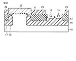
次いで、図13に示すように、ナノワイヤー-フィン18、19の露出した表面(丸める前の上面及び両側面に相当)、及びプレーナ型MOSFETの活性領域20の表面、それぞれに酸窒化膜(SiON)からなるゲート絶縁膜21、22、23を形成する。
Next, as shown in FIG. 13, the exposed surfaces of the
更に、その上に、ポリシリコン或いはメタル等のゲート電極材料を堆積し、図14に示すように、リソグラフィとRIEでゲート電極24、25を形成する。
Further, a gate electrode material such as polysilicon or metal is deposited thereon, and
本実施形態においては、フィン型FET領域のゲート電極24の高さと、プレーナ型MOSFET領域のゲート電極25の高さがほぼ同じになるので、ゲートのリソグラフィの焦点深度(DOF:Depth Of Focus)にプロセス余裕が得られる。また、フィン型FETとプレーナ型MOSFETのRIE加工を同時に行うことができる。さらにまた、ゲート表面が平坦なので、ゲートパターンの加工にサイドウォールパターントランスファー(Sidewall pattern transfer)プロセスを用いてもよい。
In the present embodiment, the height of the
本実施形態で製造されるフィン型FETにおいては、フィンの上面及び両側面がチャネルになるため、Ωゲートフィン型FETやトライゲート(Tri gate)フィン型FETに類似している。 The fin-type FET manufactured in this embodiment is similar to an Ω-gate fin-type FET or a tri-gate fin-type FET because the upper surface and both side surfaces of the fin serve as a channel.
その後、図14のゲート電極24の紙面垂直方向の両側面にスペーサを形成し、ソース/ドレインをイオン注入やシリサイド貼り付けによって形成する(図示せず)。ナノワイヤー-フィン18、19のアスペクト比は小さい。従って、フィン18、19にソース/ドレイン拡散層を形成するためのドーピングは、通常の高アスペクト比のフィンとは異なり、基板に垂直な方向とのなす角度が0〜7度となるイオン注入でよい。従って、高アスペクトのフィンに対して、チャネル幅方向(フィン高さ方向)に均一にドーピングするために必要となる斜めイオン注入技術やプラズマドーピング技術等の高価な技術が不要となるので、プロセスの低コスト化が図れる。
Thereafter, spacers are formed on both side surfaces of the
その後の製造工程は通常のLSIの製造工程と同様である。すなわち、層間絶縁膜を堆積し、コンタクトホールを形成し、上層配線(Cuなど)をダマシンプロセス等を用いて形成する(図示せず)。 The subsequent manufacturing process is the same as the normal LSI manufacturing process. That is, an interlayer insulating film is deposited, a contact hole is formed, and an upper wiring (Cu or the like) is formed using a damascene process or the like (not shown).
本実施形態に係る半導体装置の製造方法においては、(1)フィン領域、プレーナ領域のゲートのリソグラフィ、RIE加工を同時に処理可能であること、(2)バルクSi基板上のフィン型FETの製造においてフィンを出すために必要であった、フィン領域まわりの素子分離絶縁膜(STI)のリセスエッチングが不要になること、(3)フィン下部直下が酸化絶縁膜となっているので、フィン下部にパンチスルーストッパとして高濃度不純物層を形成することが不要になること、さらに(4)フィンとプレーナの作りわけのためのリソグラフィ等が不要となること、等から工程数を削減することが可能となる。 In the method of manufacturing a semiconductor device according to the present embodiment, (1) the gate region lithography and the RIE processing of the fin region and the planar region can be performed simultaneously, and (2) in the manufacture of the fin type FET on the bulk Si substrate. The need for recess etching of the element isolation insulating film (STI) around the fin region, which was necessary to bring out the fin, becomes unnecessary. (3) Since the oxide insulating film is formed directly below the fin, a punch is formed below the fin. It is possible to reduce the number of processes because it becomes unnecessary to form a high-concentration impurity layer as a through stopper, and (4) lithography and the like for making fins and planars are unnecessary. .
また、基板として安価なバルクSi基板を用いているにもかかわらず、SOI構造のナノワイヤー-フィン型FETを形成できるので、高価なSOI基板を利用しないで済むので低コスト化が図れるというメリットがある。 In addition, although an inexpensive bulk Si substrate is used as a substrate, an SOI-structured nanowire-fin type FET can be formed, which eliminates the need to use an expensive SOI substrate, thereby reducing the cost. is there.
さらにまた、深い素子分離絶縁膜(STI)と直径の小さいナノワイヤーをバルク基板上で表面高さを揃えて形成することができる。両者の高さが揃っていると、その後の製造プロセスが容易になるという長所がある。例えば、リソグラフィの焦点深度(DOF)に対する要求を緩めることができるので、解像度を高めることができる。 Furthermore, deep element isolation insulating films (STI) and nanowires with a small diameter can be formed on the bulk substrate with the same surface height. If both heights are equal, there is an advantage that the subsequent manufacturing process becomes easy. For example, the requirement for lithography depth of focus (DOF) can be relaxed, so that the resolution can be increased.
また、ゲート電極のRIE工程で、ゲート絶縁膜に対するオーバーエッチング量を低減できるので、その膜の信頼性を改善することができる。なぜなら、フィン領域(特にフィン両側面近傍)のゲートの厚さとプレーナ型MOSFET領域のゲートの厚さの差が従来のフィン型FETの場合よりも小さいので、フィン型FETのゲートをRIE加工する際、プレーナ型MOSFET領域のゲート絶縁膜がオーバーエッチングされる時間を短縮できるからである。 Further, since the amount of overetching with respect to the gate insulating film can be reduced in the RIE process of the gate electrode, the reliability of the film can be improved. This is because the difference between the gate thickness of the fin region (especially in the vicinity of both sides of the fin) and the gate thickness of the planar MOSFET region is smaller than that of the conventional fin type FET. This is because the time for overetching the gate insulating film in the planar MOSFET region can be shortened.
以上説明したように、本実施形態によれば、ナノワイヤー-フィン型FET、プレーナ型MOSFETデバイスを簡便なプロセスで、かつ低コストに混載させることが可能となる。 As described above, according to the present embodiment, it is possible to mount the nanowire-fin type FET and the planar type MOSFET device in a simple process and at low cost.
(第2の実施形態)
本発明の第2の実施形態に係る半導体装置の製造方法を、各製造工程の断面図である図15乃至図21を用いて以下に説明する。
(Second Embodiment)
A semiconductor device manufacturing method according to the second embodiment of the present invention will be described below with reference to FIGS. 15 to 21 which are cross-sectional views of the respective manufacturing steps.
本実施形態においても、ナノワイヤー-フィン型FETをプレーナ型MOSFETと同じ基板上に混載するが、ナノワイヤー-フィン型FETのゲート形成にダマシンプロセスを用い、フィンの周り全体をチャネルとするゲートオールアラウンドタイプにするところが第1の実施形態とは異なっている。 Also in this embodiment, the nanowire-fin type FET is mixedly mounted on the same substrate as the planar type MOSFET, but the gate wire is formed by using a damascene process for forming the gate of the nanowire-fin type FET and using the entire periphery of the fin as a channel. The around type is different from the first embodiment.
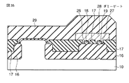
本実施形態においても図12までの工程は、第1の実施形態と同様であるので説明を省略する。その後、図15に示すように、ナノワイヤー-フィン18、19の露出した表面(丸める前の上面及び両側面に相当)の活性領域表面、及びプレーナ領域20の表面にSiO2からなるダミーゲート絶縁膜26、27、及び62を形成する。
Also in the present embodiment, the steps up to FIG. 12 are the same as those in the first embodiment, and a description thereof will be omitted. Thereafter, as shown in FIG. 15, dummy gate insulation made of SiO 2 on the exposed surface of the nanowire-
更に、その上にポリシリコン等のダミーゲート電極材料を堆積し、図16に示すように、リソグラフィとRIEでダミーゲート電極パターン28及び63を形成する。このダミーゲート28及び63は後の工程で除去するものであり、ゲート形成をダマシンプロセスで実行するために必要となる。
Further, a dummy gate electrode material such as polysilicon is deposited thereon, and dummy
その後、図16のダミーゲート28及び63の紙面垂直方向の両側面にスペーサを形成し、ソース/ドレインをイオン注入やシリサイド貼り付けによって形成する(図示せず)。本実施形態においても、アスペクト比が小さいフィン18、19にソース/ドレイン拡散層を形成するためのドーピングは、基板に垂直な方向とのなす角度が0〜7度となるイオン注入でよく、プロセスの低コスト化が図れる。
Thereafter, spacers are formed on both side surfaces of the
次に、図17に示すようにダミーゲート28及び63を含んだ全面に、TEOSを用いてSiO2膜(以下、TEOS膜)29を厚さ300nm程度堆積し、図18に示すようにCMPで平坦化して、ダミーゲート28及び63のトップを露出させる。
Next, as shown in FIG. 17, an
次いで、図19に示すようにダミーゲート28及び63をCDE(ケミカル・ドライ・エッチング)などでエッチング除去する。更に、HF(フッ酸)薬液でエッチングすると、図20に示すように、チャネル領域のSi-ナノワイヤー18、19の底部にもエッチングが進み、中空構造が形成される。即ち、ナノワイヤー18、19が橋のように空中に浮く構造となる。図20の状態を鳥瞰図で示すと図21のようになる。
Next, as shown in FIG. 19, the
ただし、図20の紙面垂直方向の手前と奥側に存在するソース・ドレイン領域がナノワイヤー18、19を支えているので、ナノワイヤー18、19がリフトオフする心配はない。この様子を、図21の点線に沿った断面図である図22に示す。
However, since the source / drain regions existing on the near side and the far side in the direction perpendicular to the paper surface of FIG. 20 support the
そして、図23に示すように、ナノワイヤー18、19の表面全面(フィンの上面、側面、底面)、及びプレーナ領域20の表面に酸窒化膜(SiON)ゲート絶縁膜30、31、及び64を形成し、さらにその上から例えばメタル材料であるゲート電極材料32及び65を堆積する。最後に、CMP平坦化して不要部分のゲート電極材料を除去する。
Then, as shown in FIG. 23, oxynitride (SiON)
このゲート電極32及び65はピュアメタルでも良いしメタルシリサイドでも良い。また、FUSI(fully silicided:完全にシリサイド化した)ゲート電極にしても良い。すなわち、ゲート溝形成後、ゲート絶縁膜を形成し、全面にポリシリコン(Poly-Si)を堆積してCMPを行ない、溝内にポリシリコンを埋め込んだ後、Niなどをスパッタしてポリシリコン全体をシリサイド化させても良い。
The
本実施形態の場合、ナノワイヤー-フィン18、19の周り全体がチャネルになるため、ゲートオールアラウンド-フィン型FETを形成することができる。
In the case of the present embodiment, since the entire area around the nanowire-
その後の製造工程は通常のLSIの製造工程と同様である。すなわち、層間絶縁膜を堆積し、コンタクトホールを形成し、上層配線(Cuなど)をダマシンプロセス等を用いて形成する(図示せず)。 The subsequent manufacturing process is the same as the normal LSI manufacturing process. That is, an interlayer insulating film is deposited, a contact hole is formed, and an upper wiring (Cu or the like) is formed using a damascene process or the like (not shown).
本実施形態に係る半導体装置の製造方法においても、第1の実施形態と同様の理由によって、工程数を削減することが可能となる。また同様に、安価なバルクSi基板にSOI構造のナノワイヤー-フィン型FETを形成できるので、高価なSOI基板を利用しないで済むので低コスト化が図れる。 Also in the method for manufacturing a semiconductor device according to the present embodiment, the number of steps can be reduced for the same reason as in the first embodiment. Similarly, since a nanowire-fin type FET having an SOI structure can be formed on an inexpensive bulk Si substrate, it is not necessary to use an expensive SOI substrate, so that the cost can be reduced.
さらにまた、深い素子分離絶縁膜(STI)と直径の小さいナノワイヤーをバルク基板上で表面高さを揃えて形成することができるので、その後の製造プロセスが容易になる。例えば、リソグラフィの焦点深度(DOF)に対する要求を緩めることができるので、解像度を高めることができる。また、ゲート電極のRIE工程で、ゲート絶縁膜に対するオーバーエッチング量を低減できるので、その膜の信頼性を改善することができる。 Furthermore, since the deep element isolation insulating film (STI) and the nanowire with a small diameter can be formed on the bulk substrate with the same surface height, the subsequent manufacturing process becomes easy. For example, the requirement for lithography depth of focus (DOF) can be relaxed, so that the resolution can be increased. Further, since the amount of overetching with respect to the gate insulating film can be reduced in the RIE process of the gate electrode, the reliability of the film can be improved.
さらにまた、ナノワイヤー-フィンの周り全体がチャネルになるため、ゲートオールアラウンド-フィン型FETを形成することができ、トランジスタの微細化、高性能化を押し進めることができる。 Furthermore, since the entire area around the nanowire-fin is a channel, a gate all-around-fin type FET can be formed, and the miniaturization and high performance of the transistor can be promoted.
以上説明したように、本実施形態によれば、ナノワイヤー-フィン型FET、プレーナ型MOSFETデバイスを簡便なプロセスで、かつ低コストに混載させることが可能となる。 As described above, according to the present embodiment, it is possible to mount the nanowire-fin type FET and the planar type MOSFET device in a simple process and at low cost.
上記実施形態においては、ナノワイヤー-フィン型FETのゲート形成にダマシンプロセスを適用しつつ、ナノワイヤー-フィン型FETをプレーナ型MOSFETと同じ基板上に混載する際の製造コストを削減している。したがって、以下のような変形例も挙げられる。 In the above embodiment, the damascene process is applied to the gate formation of the nanowire-fin type FET, and the manufacturing cost when the nanowire-fin type FET is mixedly mounted on the same substrate as the planar MOSFET is reduced. Therefore, the following modifications are also possible.
まず、第1の変形例を、図24乃至図28を用いて説明する。第1の変形例は、図18までの工程は上記実施形態と同じである。そのあと、ポリシリコン等からなるダミーゲート28及び63にドーパントをイオン注入し、その後、活性化アニールを行う(図示せず)。
First, a first modification will be described with reference to FIGS. In the first modification, the steps up to FIG. 18 are the same as those in the above embodiment. Thereafter, dopant is ion-implanted into
さらに、図24に示すように、ポリシリコンプレーナ領域をレジスト66で覆い、ダミーゲート28をCDE(ケミカル・ドライ・エッチング)などでエッチング除去することによりフィン領域を開口する。その後、レジスト66を剥離して、HF(フッ酸)薬液でエッチングすると、図25に示すように、チャネル領域のSi-ナノワイヤー18、19の底部にもエッチングが進み、中空構造が形成される。図25の状態を鳥瞰図で示すと図26のようになる。
Further, as shown in FIG. 24, the polysilicon planar region is covered with a resist 66, and the
そして、図27に示すように、ナノワイヤー18、19の表面全面(フィンの上面、側面、底面)に酸窒化膜(SiON)ゲート絶縁膜30、31を形成し、さらにその上から例えばメタル材料であるゲート電極材料32を堆積する。最後に、CMP平坦化して不要部分のゲート電極材料32を除去すると、図28に示すように、プレーナ領域がポリシリコン電極63で、フィン領域がメタル電極32となる。その後の製造工程は通常のLSIの製造工程と同様である。
Then, as shown in FIG. 27, oxynitride (SiON)
次に、第2の変形例を、図29乃至図30を用いて説明する。第2の変形例も、図28までの工程は第1の変形例と同じで、プレーナ領域がポリシリコン電極で、フィン領域がメタル電極のFETある。ただし、図18において第1の変形例で行ったポリシリコン等からなるダミーゲート28及び63へのドーピングは行わなくとも良い。
Next, a second modification will be described with reference to FIGS. In the second modification, the steps up to FIG. 28 are the same as those in the first modification, and the planar region is a polysilicon electrode and the fin region is a metal electrode. However, the doping to the
まず、図28の状態で、図29に示すようにNi70をスパッタし、その後、アニールする。次に、図30に示すように、硫酸と過酸化水素水の混合溶液で余剰のNi70を剥離する。ポリシリコン領域63は上記アニールによってNiシリサイド71になっている。この時のアニール温度は300℃〜600℃程度が望ましく、典型的には500℃である。
First, in the state of FIG. 28, Ni70 is sputtered as shown in FIG. 29, and then annealed. Next, as shown in FIG. 30,
このとき、作り易さの点から、フィン領域のメタル電極32は500℃のアニールでNi70と反応しにくい材料が望ましい。また、仕事関数制御の点から、シリサイド時のアニール温度でNiと反応しうる材料を用いる際には、アニール温度でNiと反応しにくい材料をキャップ膜として、2層構造にすることが望ましい。Niと反応しにくい材料としては、例えば、TiN、TaN、WN、AlN、HfC、HfB、TaC及びこれらの混合物などが挙げられる。
At this time, from the viewpoint of ease of manufacturing, the
さらに、熱的安定性の向上、仕事関数の調整のため、C、Cr、Fe、Ge、B、P、As、Sn、Ga、In、P,Sb、S、Cl、Fなどを添加しても良い。Niと反応しうる材料としては、例えば、Co、Ni、Pt、Ti、Hf、Zr、Ta、W、Mo、Al及びこれらの合金、これらの材料とSiとの混合物が挙げられる。仕事関数の調整のため、上述の同様の添加剤を混ぜても良い。 Furthermore, C, Cr, Fe, Ge, B, P, As, Sn, Ga, In, P, Sb, S, Cl, F, etc. are added to improve thermal stability and work function. Also good. Examples of the material capable of reacting with Ni include Co, Ni, Pt, Ti, Hf, Zr, Ta, W, Mo, Al, and alloys thereof, and a mixture of these materials and Si. In order to adjust the work function, the same additive as described above may be mixed.
本変形例によると、図30に示すように、プレーナ領域がNiシリサイド電極71で、フィン領域がメタル電極32となる。その後の製造工程は通常のLSIの製造工程と同様である。
According to this modification, as shown in FIG. 30, the planar region is the
さらに、第3の変形例を図31乃至図33を用いて説明する。第3の変形例も、図28までの工程は第1の変形例と同じで、プレーナ領域がポリシリコン電極で、フィン領域がメタル電極のFETである。ただし、図18において第1の変形例で行ったポリシリコン等からなるダミーゲート28及び63へのドーピングは行わなくとも良い。
Further, a third modification will be described with reference to FIGS. In the third modification, the steps up to FIG. 28 are the same as those in the first modification, and the planar region is a polysilicon electrode and the fin region is a metal electrode. However, the doping to the
まず、図28の状態で、図31に示すようにCDEなどでプレーナ領域のポリシリコン63を剥離する。次に、図32に示すように、プレーナ用のメタル電極33を成膜する。メタル電極33の材料は、フィン領域のゲート電極材料に用いるメタル材料として挙げたものから選択することができ、フィン領域と同じでも、異なっても構わない。
First, in the state of FIG. 28, the
さらに、図33に示すようにCMPで平坦化する。その結果、プレーナ領域、フィン領域がともにメタル電極となる。その後の製造工程は通常のLSIの製造工程と同様である。 Further, planarization is performed by CMP as shown in FIG. As a result, both the planar region and the fin region become metal electrodes. The subsequent manufacturing process is the same as the normal LSI manufacturing process.
さらに、第4の変形例を、図34乃至42を用いて説明する。第4の変形例は、図15でダミーゲート絶縁膜26、27、及び62を形成するところまでは、本(第2の)実施形態と同様である。
Further, a fourth modification will be described with reference to FIGS. The fourth modification is the same as that of the present (second) embodiment until the dummy
その後、図34に示すようにフィン領域のダミーゲートポリシリコン28を加工形成し、図35に示すように、TEOS膜29を成膜する。さらに、図36に示すように、CMPで平坦化する。次いで、図37に示すようにフィン領域のダミーゲート28をCDEで剥離し、さらに、図38に示すように、HF薬液でエッチングする。
Thereafter, the
その後、ナノワイヤー18、19の表面全面に酸窒化膜(SiON)ゲート絶縁膜30、31を形成し、メタル材料32を成膜して、CMPで平坦化すると同時に、プレーナ領域の余剰メタルを剥離することにより、図39の構造を得る。
Thereafter, an oxynitride (SiON)
次いで、図40に示すように、プレーナ領域のゲート形状にTEOS膜29に溝75を形成する。溝75は、リソグラフィ法を用いて、プレーナ領域上にゲート形状にレジスト(図示せず)を開口し、RIEでTEOS膜29をエッチングすることで得られる。RIEだけでなく、HFによるエッチングと組み合わせても良い。
Next, as shown in FIG. 40, a
次いで、図41に示すように、ゲート絶縁膜76とメタル電極42を成膜する。最後に、図42に示すように、CMPで平坦化すると同時に、フィン領域の余剰メタルを剥離する。その結果、プレーナ領域、フィン領域がともにメタル電極42、32となる。その後の製造工程は通常のLSIの製造工程と同様である。
Next, as shown in FIG. 41, a
以上説明したように、本実施形態の変形例によっても、ナノワイヤー-フィン型FET、プレーナ型MOSFETデバイスを簡便なプロセスで、かつ低コストに混載させることが可能となる。 As described above, according to the modification of the present embodiment, the nanowire-fin type FET and the planar type MOSFET device can be mixed in a simple process and at low cost.
(第3の実施形態)
本発明の第3の実施形態に係る半導体装置の製造方法を、図43乃至図57を用いて以下に説明する。
(Third embodiment)
A method for manufacturing a semiconductor device according to the third embodiment of the present invention will be described below with reference to FIGS.
本実施形態においては、図1に示したようなナノワイヤー-フィン型FETのフィンの両端にプレーナ領域を同時形成する。 In the present embodiment, planar regions are simultaneously formed at both ends of the fin of the nanowire-fin type FET as shown in FIG.
本実施形態においても、第1の実施形態の図2乃至図11までの工程と基本的に同様な工程が実行される。しかし、本実施形態においては図3とは異なって、図43の上面図に示すような、ナノワイヤー-フィンの両端に当該フィンより横幅の広いプレーナ領域が接続された形状であるハードマスク35をバルクSi基板10の上に形成する。
Also in the present embodiment, basically the same processes as those in FIGS. 2 to 11 of the first embodiment are performed. However, in this embodiment, unlike FIG. 3, a
ここで、ハードマスク35は例えば、膜厚50nm程度のSiN膜であるが、SiO2、あるいはSiON、更にはSiN/SiO2/SiN等の積層膜、その他の絶縁膜であってもかまわない。図43のB−B’線に沿った断面図及びA−A’線に沿った断面図を図44に示す。
Here, the
その後、第1の実施形態の図4乃至図11までの工程と同様に、図43のB−B’線に沿った断面(プレーナ領域)及びA−A’線に沿った断面(フィン領域)で見た図45乃至図52に示される工程が実行される。 Thereafter, similarly to the steps from FIG. 4 to FIG. 11 of the first embodiment, the cross section along the line BB ′ in FIG. 43 (planar region) and the cross section along the line AA ′ (fin region). The steps shown in FIGS. 45 to 52 seen in FIG.
まず、ハードマスク35をマスクとしてRIE加工を行なうことにより図45に示すように、20nm程度の深さの溝がバルクSi基板10に形成される。ここでは、図45(a)、(b)共に両側の溝の途中までしか示していない。図45(a)、(b)は、例えば、図43で示したハードマスク35が複数並列しており、そのため図45(a)、(b)の左右にそれと同様な構造が並列していて、その一部の断面を示しているとしてもよい。以下も同様とする。
First, by performing RIE processing using the
次に、図46に示すように、この上からSiN膜14を全面に形成した後、図47に示すようにエッチバックすることにより溝の側面に厚さ20nm程度のSiNの側壁絶縁膜14を形成する。側壁絶縁膜14としては、SiO2、SiON、或いはその他の絶縁膜を用いてもかまわない。
Next, as shown in FIG. 46, an
次いで、図48に示すようにハードマスク35と側壁絶縁膜14をマスクとしてSi基板10をエッチングして溝をさらに深く掘る。
Next, as shown in FIG. 48, the
次に、図49に示すようにハードマスク35と側壁絶縁膜14を耐酸化性マスクとして溝底部に露出したSi基板10の表面を酸化して酸化膜16を形成する。その際、フィン型FET領域においてシリコンフィン底部の両側面からの酸化膜16が互いに接するように酸化膜厚を調整する。
Next, as shown in FIG. 49, an
その結果フィン型FET領域のみ部分的に、酸化膜16の上に半導体領域であるフィン領域18が残存する構造、即ちSOI構造が形成される。他方、幅が広くなるように形成したプレーナ領域では、両側壁からの酸化膜が接しないのでSOI構造とはならない。
As a result, a structure in which the
次に図50に示すように、HDP(High Density Plasma:高密度プラズマ)などを用いてSiO2系絶縁膜からなる素子分離絶縁膜(STI)17を全面に堆積し、更にCMP(Chemical Mechanical Polishing:化学的機械的研磨)平坦化を実行して、SiNハードマスク35を露出させる。そしてさらに、図51に示すように素子分離絶縁膜(STI)17をエッチングする。
Next, as shown in FIG. 50, an element isolation insulating film (STI) 17 composed of a SiO 2 insulating film is deposited on the entire surface using HDP (High Density Plasma) or the like, and further CMP (Chemical Mechanical Polishing). : Chemical mechanical polishing) Planarization is performed to expose the SiN
次いで、図52に示すように、SiNハードマスク35及びSiN側壁絶縁膜14をホットリン酸などで除去することにより、フィン型FET領域においてはフィン18の上面および両側面が露出する。
Next, as shown in FIG. 52, the upper surface and both side surfaces of the
以上のように本実施形態においても、フィン型FETとプレーナ領域のRIE加工を同時に行なうことができる。 As described above, also in this embodiment, the RIE processing of the fin-type FET and the planar region can be performed simultaneously.
図53は、図52の工程まで進んだ時の、図52(a)及び(b)に示したC−C’線に沿って切り出した半導体装置の3次元構造を示した斜視図である。ナノワイヤー-フィン18の両端には、フィン18より横幅が大きいプレーナ領域20がそれぞれ接続されている。
FIG. 53 is a perspective view showing a three-dimensional structure of the semiconductor device cut out along the line C-C ′ shown in FIGS. 52A and 52B when the process proceeds to the step of FIG. 52.
この後、A−A’線に沿った断面図である図54に示すようにナノワイヤー-フィン18の上面及び両側面に、例えば、酸窒化膜(SiON)等からなるゲート絶縁膜36を形成する。
Thereafter, as shown in FIG. 54 which is a cross-sectional view along the line AA ′, a
更にその上に、ポリシリコン或いはメタル等のゲート電極材料を堆積し、図55に示すように、リソグラフィとRIEでゲート電極37を形成する。図56は、図55に示したC−C’線に沿って切り出した半導体装置の3次元構造を示した斜視図である。
Further, a gate electrode material such as polysilicon or metal is deposited thereon, and a
その後、図55のゲート電極37の紙面垂直方向の両側面にスペーサを形成し、ソース/ドレインをイオン注入やシリサイド貼り付けによって形成する(図示せず)。ナノワイヤー-フィン型FETのフィン18のアスペクト比は小さいので、ソース/ドレイン拡散層を形成するためのドーピングは、基板に垂直な方向とのなす角度が0〜7度となるイオン注入でよい。従って、斜めイオン注入技術やプラズマドーピング技術等の高価な技術が不要となるので、プロセスの低コスト化が図れる。
Thereafter, spacers are formed on both side surfaces of the
本実施形態で製造されるフィン型FETは、フィンの上面及び両側面がチャネルになるため、トライゲート(Tri gate)フィン型FETとなっている。 The fin-type FET manufactured in this embodiment is a tri-gate fin-type FET because the upper surface and both side surfaces of the fin serve as channels.
その後、図57に示すように、層間絶縁膜を堆積し(図示せず)、上層配線(Cuなど)と接続するためのコンタクト38を形成する。ここで、プレーナ領域20の横幅がナノワイヤー-フィン18の横幅より大きくなるように形成されているため、コンタクト38とソース/ドレイン領域40との界面抵抗を小さくすることができる。
Thereafter, as shown in FIG. 57, an interlayer insulating film is deposited (not shown), and a
また、コンタクトの位置合わせにずれが生じてコンタクト39のように形成されたとしても、プレーナ領域20との接触が維持され、合わせずれに強い構造となっている。
Further, even if the contact is misaligned and formed like the
以上述べたように、フィン型FETとプレーナ領域を同時形成する本実施形態によって、第1及び第2の実施形態と同様な工程の削減と低コスト化が図れると同時に、コンタクトとの界面抵抗が小さく、合わせずれに強いナノワイヤー-フィン型FETを備えた半導体装置の製造が可能となる。 As described above, the present embodiment in which the fin-type FET and the planar region are formed at the same time can reduce the process and cost as in the first and second embodiments, and at the same time reduce the interface resistance with the contact. It is possible to manufacture a semiconductor device having a nanowire-fin type FET that is small and resistant to misalignment.
なお、本願発明は上記実施形態に限定されるものではなく、実施段階ではその要旨を逸脱しない範囲で種々に変形することが可能である。更に、上記実施形態には種々の段階の発明が含まれており、開示される複数の構成要件における適宜な組み合わせにより種々の発明が抽出されうる。例えば、実施形態に示される全構成要件からいくつかの構成要件が削除されても、発明が解決しようとする課題の欄で述べた課題が解決でき、発明の効果の欄で述べられている効果が得られる場合には、この構成要件が削除された構成が発明として抽出されうる。 Note that the present invention is not limited to the above-described embodiment, and various modifications can be made without departing from the scope of the invention in the implementation stage. Further, the above embodiments include inventions at various stages, and various inventions can be extracted by appropriately combining a plurality of disclosed constituent elements. For example, even if some constituent requirements are deleted from all the constituent requirements shown in the embodiment, the problem described in the column of the problem to be solved by the invention can be solved, and the effect described in the column of the effect of the invention Can be extracted as an invention.
10…バルクSi基板、11、12、13、35…ハードマスク、14…側壁絶縁膜、
15…SiNハードマスク材、16…酸化膜、17…素子分離絶縁膜(STI)、
18、19…ナノワイヤー-フィン、20…プレーナ領域、
21、22、23、36、76…ゲート絶縁膜、
24、25、32、33、37、42、65…ゲート電極、
26、27、62…ダミーゲート絶縁膜、28、63…ダミーゲート、29…TEOS膜
30、31、64…酸窒化膜ゲート絶縁膜、38、39…コンタクト、
40…ドレイン領域、50…第1の溝、60…第2の溝、66…レジスト、
70…Ni、71…Niシリサイド、75…溝、メタル電極。
DESCRIPTION OF
15 ... SiN hard mask material, 16 ... oxide film, 17 ... element isolation insulating film (STI),
18, 19 ... nanowire-fin, 20 ... planar region,
21, 22, 23, 36, 76 ... gate insulating film,
24, 25, 32, 33, 37, 42, 65 ... gate electrodes,
26, 27, 62 ... dummy gate insulating film, 28, 63 ... dummy gate, 29 ...
40 ... drain region, 50 ... first groove, 60 ... second groove, 66 ... resist,
70 ... Ni, 71 ... Ni silicide, 75 ... groove, metal electrode.
Claims (5)
前記ライン状の絶縁膜をマスクとして前記半導体基板をエッチングすることにより前記ライン状の絶縁膜の両側に2つの隣接する第1の溝を形成する工程と、
隣接する前記第1の溝それぞれの側壁に側壁絶縁膜を形成する工程と、
前記ライン状の絶縁膜及び前記側壁絶縁膜をマスクとして前記半導体基板をエッチングすることにより隣接する前記第1の溝の底部それぞれに第2の溝を形成する工程と、
前記ライン状の絶縁膜及び前記側壁絶縁膜を耐酸化性マスクとして前記半導体基板を酸化することにより、前記第2の溝の前記半導体基板を挟んで隣接する側壁それぞれに形成される酸化領域を互いに接触させる工程と、
前記ライン状の絶縁膜及び前記側壁絶縁膜を除去する工程と、
前記除去によって露出した前記半導体基板の半導体領域の表面にゲート絶縁膜を形成する工程と、
前記ゲート絶縁膜の上にゲート電極を形成する工程と、
前記半導体領域をライン状のフィンとするフィン型電界効果トランジスタを形成する工程と
を含むことを特徴とする半導体装置の製造方法。 Forming a line-shaped insulating film on the main surface of the semiconductor substrate;
Forming two adjacent first grooves on both sides of the line-shaped insulating film by etching the semiconductor substrate using the line-shaped insulating film as a mask;
Forming a sidewall insulating film on the sidewall of each of the adjacent first grooves;
Forming a second groove on each bottom of the adjacent first groove by etching the semiconductor substrate using the line-shaped insulating film and the sidewall insulating film as a mask;
By oxidizing the semiconductor substrate using the line-shaped insulating film and the sidewall insulating film as an oxidation-resistant mask, the oxidized regions formed on the sidewalls adjacent to each other across the semiconductor substrate in the second groove are mutually connected. A step of contacting;
Removing the line-shaped insulating film and the sidewall insulating film;
Forming a gate insulating film on the surface of the semiconductor region of the semiconductor substrate exposed by the removal;
Forming a gate electrode on the gate insulating film;
Forming a fin-type field effect transistor having the semiconductor region as a line-shaped fin.
前記第1及び第2の絶縁膜をマスクとして前記半導体基板をエッチングすることにより前記第1及び第2の絶縁膜の両側に複数の第1の溝を形成する工程と、
複数の前記第1の溝それぞれの側壁に側壁絶縁膜を形成する工程と、
前記第1及び第2の絶縁膜及び前記側壁絶縁膜をマスクとして前記半導体基板をエッチングすることにより複数の前記第1の溝の底部それぞれに第2の溝を形成する工程と、
前記第1及び第2の絶縁膜及び前記側壁絶縁膜を耐酸化性マスクとして前記半導体基板を酸化することにより、前記第1の絶縁膜の両側の前記第2の溝の前記半導体基板を挟んで隣接する側壁それぞれに形成される酸化領域を互いに接触させ、前記第2の絶縁膜の両側の前記第2の溝の前記半導体基板を挟んで隣接する側壁それぞれに形成される酸化領域は互いに接触させない工程と、
前記第1及び第2の絶縁膜及び前記側壁絶縁膜を除去する工程と、
前記第1の絶縁膜の除去によって露出した前記半導体基板の半導体領域の表面にゲート絶縁膜を形成し、前記ゲート絶縁膜の上にゲート電極を形成することにより、前記半導体領域をライン状のフィンとするフィン型電界効果トランジスタを形成する工程と、
前記第2の絶縁膜の除去によって露出した前記半導体基板の別の半導体領域にプレーナ型電界効果トランジスタ或いはプレーナ領域を形成する工程と
を含むことを特徴とする半導体装置の製造方法。 Simultaneously forming a line-shaped first insulating film and a second insulating film having a larger line width than the first insulating film on the main surface of the semiconductor substrate;
Forming a plurality of first grooves on both sides of the first and second insulating films by etching the semiconductor substrate using the first and second insulating films as a mask;
Forming a sidewall insulating film on a sidewall of each of the plurality of first grooves;
Forming a second groove on each of the bottoms of the plurality of first grooves by etching the semiconductor substrate using the first and second insulating films and the sidewall insulating film as a mask;
By oxidizing the semiconductor substrate using the first and second insulating films and the sidewall insulating film as an oxidation resistant mask, the semiconductor substrate in the second groove on both sides of the first insulating film is sandwiched. Oxide regions formed on adjacent side walls are brought into contact with each other, and oxidized regions formed on adjacent side walls across the semiconductor substrate of the second groove on both sides of the second insulating film are not in contact with each other. Process,
Removing the first and second insulating films and the sidewall insulating film;
A gate insulating film is formed on the surface of the semiconductor region of the semiconductor substrate exposed by the removal of the first insulating film, and a gate electrode is formed on the gate insulating film, whereby the semiconductor region is formed into a line-shaped fin. A step of forming a fin-type field effect transistor,
Forming a planar field effect transistor or a planar region in another semiconductor region of the semiconductor substrate exposed by the removal of the second insulating film.
前記フィンとなるべき前記半導体領域の下の前記酸化領域の前記半導体領域に接している部分を除去する工程を
更に含むことを特徴とする請求項1又は2に記載の半導体装置の製造方法。 After the removing step and before forming the gate insulating film,
The method of manufacturing a semiconductor device according to claim 1, further comprising a step of removing a portion of the oxide region that is in contact with the semiconductor region under the semiconductor region to be the fin.
水素を含んだ雰囲気中でアニールすることにより前記フィンとなるべき前記半導体領域の断面形状を丸める工程を更に含むことを特徴とする請求項1乃至3のいずれか1項に記載の半導体装置の製造方法。 After the removing step and before forming the gate insulating film,
4. The method of manufacturing a semiconductor device according to claim 1, further comprising a step of rounding a cross-sectional shape of the semiconductor region to be the fin by annealing in an atmosphere containing hydrogen. Method.
前記シリコン酸化膜上に形成されたライン状のフィンと、
前記フィンの延伸方向の両端にそれぞれ接続され、前記延伸方向と垂直な方向の幅が前記フィンよりも大きく、上面の高さが前記フィンの上面の高さと一致している前記基板の一部であるプレーナ領域と
を具備することを特徴とした半導体装置。 A silicon oxide film formed on a bulk silicon substrate;
A line-shaped fin formed on the silicon oxide film;
A part of the substrate that is connected to both ends of the fin in the extending direction, the width in the direction perpendicular to the extending direction is larger than the fin, and the height of the upper surface coincides with the height of the upper surface of the fin; A semiconductor device comprising: a planar region.
Priority Applications (3)
| Application Number | Priority Date | Filing Date | Title |
|---|---|---|---|
| JP2007004672A JP2008172082A (en) | 2007-01-12 | 2007-01-12 | Semiconductor device and manufacturing method of semiconductor device |
| US11/972,097 US7820551B2 (en) | 2007-01-12 | 2008-01-10 | Semiconductor device having fins FET and manufacturing method thereof |
| US12/923,308 US20110012201A1 (en) | 2007-01-12 | 2010-09-14 | Semiconductor device having fins FET and manufacturing method thereof |
Applications Claiming Priority (1)
| Application Number | Priority Date | Filing Date | Title |
|---|---|---|---|
| JP2007004672A JP2008172082A (en) | 2007-01-12 | 2007-01-12 | Semiconductor device and manufacturing method of semiconductor device |
Publications (1)
| Publication Number | Publication Date |
|---|---|
| JP2008172082A true JP2008172082A (en) | 2008-07-24 |
Family
ID=39685091
Family Applications (1)
| Application Number | Title | Priority Date | Filing Date |
|---|---|---|---|
| JP2007004672A Pending JP2008172082A (en) | 2007-01-12 | 2007-01-12 | Semiconductor device and manufacturing method of semiconductor device |
Country Status (2)
| Country | Link |
|---|---|
| US (2) | US7820551B2 (en) |
| JP (1) | JP2008172082A (en) |
Cited By (9)
| Publication number | Priority date | Publication date | Assignee | Title |
|---|---|---|---|---|
| JP2012028420A (en) * | 2010-07-20 | 2012-02-09 | Toshiba Corp | Semiconductor device and manufacturing method of the same |
| WO2012132219A1 (en) * | 2011-03-29 | 2012-10-04 | ルネサスエレクトロニクス株式会社 | Semiconductor device and manufacturing method for same |
| US8314464B2 (en) | 2009-09-16 | 2012-11-20 | Kabushiki Kaisha Toshiba | Semiconductor device and manufacturing method thereof |
| JP2013048161A (en) * | 2011-08-29 | 2013-03-07 | Citizen Holdings Co Ltd | Semiconductor device manufacturing method |
| JP2013513249A (en) * | 2009-12-18 | 2013-04-18 | インテル・コーポレーション | Insulation of nanowire devices |
| JP2013528931A (en) * | 2010-04-13 | 2013-07-11 | インターナショナル・ビジネス・マシーンズ・コーポレーション | Nanowire circuits in matched devices |
| JP2014505995A (en) * | 2010-12-01 | 2014-03-06 | インテル コーポレイション | Nanowire structure of silicon and silicon germanium |
| JP2016541114A (en) * | 2013-12-19 | 2016-12-28 | インテル・コーポレーション | Self-aligned gate edges and local interconnects and methods of manufacturing the same |
| JP2019525484A (en) * | 2016-08-08 | 2019-09-05 | 東京エレクトロン株式会社 | Three-dimensional semiconductor device and manufacturing method |
Families Citing this family (28)
| Publication number | Priority date | Publication date | Assignee | Title |
|---|---|---|---|---|
| JP2008172082A (en) * | 2007-01-12 | 2008-07-24 | Toshiba Corp | Semiconductor device and manufacturing method of semiconductor device |
| US8106459B2 (en) | 2008-05-06 | 2012-01-31 | Taiwan Semiconductor Manufacturing Company, Ltd. | FinFETs having dielectric punch-through stoppers |
| US8048723B2 (en) | 2008-12-05 | 2011-11-01 | Taiwan Semiconductor Manufacturing Company, Ltd. | Germanium FinFETs having dielectric punch-through stoppers |
| US8263462B2 (en) * | 2008-12-31 | 2012-09-11 | Taiwan Semiconductor Manufacturing Company, Ltd. | Dielectric punch-through stoppers for forming FinFETs having dual fin heights |
| KR101078725B1 (en) * | 2009-02-16 | 2011-11-01 | 주식회사 하이닉스반도체 | Semiconductor device and method of manufacturing the same |
| US8293616B2 (en) | 2009-02-24 | 2012-10-23 | Taiwan Semiconductor Manufacturing Company, Ltd. | Methods of fabrication of semiconductor devices with low capacitance |
| US8455334B2 (en) * | 2009-12-04 | 2013-06-04 | International Business Machines Corporation | Planar and nanowire field effect transistors |
| US8722492B2 (en) | 2010-01-08 | 2014-05-13 | International Business Machines Corporation | Nanowire pin tunnel field effect devices |
| US9029834B2 (en) | 2010-07-06 | 2015-05-12 | International Business Machines Corporation | Process for forming a surrounding gate for a nanowire using a sacrificial patternable dielectric |
| US8354319B2 (en) * | 2010-10-15 | 2013-01-15 | International Business Machines Corporation | Integrated planar and multiple gate FETs |
| US8524545B2 (en) | 2010-10-22 | 2013-09-03 | International Business Machines Corporation | Simultaneous formation of FinFET and MUGFET |
| US8524546B2 (en) | 2010-10-22 | 2013-09-03 | International Business Machines Corporation | Formation of multi-height MUGFET |
| US8580694B2 (en) * | 2011-08-25 | 2013-11-12 | United Microelectronics Corp. | Method of patterning hard mask layer for defining deep trench |
| CN103579318B (en) * | 2012-08-10 | 2016-05-04 | 南亚科技股份有限公司 | Multi-gate transistor and manufacturing method thereof |
| US8541274B1 (en) * | 2012-09-11 | 2013-09-24 | Globalfoundries Inc. | Methods of forming 3-D semiconductor devices with a nanowire gate structure wherein the nanowire gate structure is formed after source/drain formation |
| US8580634B1 (en) * | 2012-09-11 | 2013-11-12 | Globalfoundries Inc. | Methods of forming 3-D semiconductor devices with a nanowire gate structure wherein the nanowire gate structure is formed prior to source/drain formation |
| US8853019B1 (en) | 2013-03-13 | 2014-10-07 | Globalfoundries Inc. | Methods of forming a semiconductor device with a nanowire channel structure by performing an anneal process |
| US9263554B2 (en) * | 2013-06-04 | 2016-02-16 | International Business Machines Corporation | Localized fin width scaling using a hydrogen anneal |
| US9000498B2 (en) * | 2013-06-28 | 2015-04-07 | Stmicroelectronics, Inc. | FinFET with multiple concentration percentages |
| US8951850B1 (en) * | 2013-08-21 | 2015-02-10 | International Business Machines Corporation | FinFET formed over dielectric |
| CN105765703B (en) | 2013-12-23 | 2021-02-23 | 英特尔公司 | Etching techniques for straight, tall, and uniform fins among multiple fin pitch structures |
| US9490340B2 (en) | 2014-06-18 | 2016-11-08 | Globalfoundries Inc. | Methods of forming nanowire devices with doped extension regions and the resulting devices |
| US9431512B2 (en) | 2014-06-18 | 2016-08-30 | Globalfoundries Inc. | Methods of forming nanowire devices with spacers and the resulting devices |
| US9698025B2 (en) * | 2014-09-04 | 2017-07-04 | Globalfoundries Inc. | Directed self-assembly material growth mask for forming vertical nanowires |
| CN105097938B (en) * | 2015-08-11 | 2018-10-16 | 上海华力微电子有限公司 | A kind of fin field effect pipe and forming method thereof |
| KR20170103067A (en) * | 2016-03-02 | 2017-09-13 | 삼성전자주식회사 | Semiconductor device having MOS-transistor |
| DE112017007751T5 (en) * | 2017-08-17 | 2020-04-16 | Intel Corporation | STRUCTURING AN INTEGRATED NANO WIRE & NANOBAND IN TRANSISTOR MANUFACTURING |
| US12477841B2 (en) * | 2022-03-17 | 2025-11-18 | Taiwan Semiconductor Manufacturing Company Ltd. | Semiconductor image-sensing structure and method for forming the same |
Citations (13)
| Publication number | Priority date | Publication date | Assignee | Title |
|---|---|---|---|---|
| JPH06342911A (en) * | 1993-06-01 | 1994-12-13 | Oki Electric Ind Co Ltd | Manufacture of semiconductor device |
| JPH0786595A (en) * | 1993-09-14 | 1995-03-31 | Fujitsu Ltd | Semiconductor device and manufacturing method thereof |
| JPH07153837A (en) * | 1993-11-30 | 1995-06-16 | Sony Corp | Semiconductor device and method of manufacturing semiconductor device |
| JPH09246507A (en) * | 1996-03-05 | 1997-09-19 | Citizen Watch Co Ltd | Semiconductor device and its manufacture |
| JPH1117001A (en) * | 1997-06-18 | 1999-01-22 | Internatl Business Mach Corp <Ibm> | Semiconductor device and manufacturing method thereof |
| JPH1168069A (en) * | 1997-04-04 | 1999-03-09 | Nippon Steel Corp | Semiconductor device and manufacturing method thereof |
| JP2000058802A (en) * | 1998-01-13 | 2000-02-25 | Stmicroelectronics Srl | SOI wafer manufacturing method |
| JP2002118255A (en) * | 2000-07-31 | 2002-04-19 | Toshiba Corp | Semiconductor device and manufacturing method thereof |
| JP2002151688A (en) * | 2000-08-28 | 2002-05-24 | Mitsubishi Electric Corp | MOS type semiconductor device and method of manufacturing the same |
| WO2005020325A1 (en) * | 2003-08-26 | 2005-03-03 | Nec Corporation | Semiconductor device and manufacturing method thereof |
| JP2005229107A (en) * | 2004-02-10 | 2005-08-25 | Samsung Electronics Co Ltd | Field effect transistor and manufacturing method thereof |
| JP2006080519A (en) * | 2004-09-07 | 2006-03-23 | Samsung Electronics Co Ltd | Field effect transistor having wire channel and method of manufacturing the same |
| JP2006522486A (en) * | 2003-04-03 | 2006-09-28 | アドバンスト・マイクロ・ディバイシズ・インコーポレイテッド | Method for forming a gate in a FinFET device and method for thinning fins in the channel region of the FinFET device |
Family Cites Families (5)
| Publication number | Priority date | Publication date | Assignee | Title |
|---|---|---|---|---|
| US7326619B2 (en) * | 2003-08-20 | 2008-02-05 | Samsung Electronics Co., Ltd. | Method of manufacturing integrated circuit device including recessed channel transistor |
| US7393733B2 (en) * | 2004-12-01 | 2008-07-01 | Amberwave Systems Corporation | Methods of forming hybrid fin field-effect transistor structures |
| US7488650B2 (en) * | 2005-02-18 | 2009-02-10 | Infineon Technologies Ag | Method of forming trench-gate electrode for FinFET device |
| JP4648096B2 (en) * | 2005-06-03 | 2011-03-09 | 株式会社東芝 | Manufacturing method of semiconductor device |
| JP2008172082A (en) * | 2007-01-12 | 2008-07-24 | Toshiba Corp | Semiconductor device and manufacturing method of semiconductor device |
-
2007
- 2007-01-12 JP JP2007004672A patent/JP2008172082A/en active Pending
-
2008
- 2008-01-10 US US11/972,097 patent/US7820551B2/en active Active
-
2010
- 2010-09-14 US US12/923,308 patent/US20110012201A1/en not_active Abandoned
Patent Citations (13)
| Publication number | Priority date | Publication date | Assignee | Title |
|---|---|---|---|---|
| JPH06342911A (en) * | 1993-06-01 | 1994-12-13 | Oki Electric Ind Co Ltd | Manufacture of semiconductor device |
| JPH0786595A (en) * | 1993-09-14 | 1995-03-31 | Fujitsu Ltd | Semiconductor device and manufacturing method thereof |
| JPH07153837A (en) * | 1993-11-30 | 1995-06-16 | Sony Corp | Semiconductor device and method of manufacturing semiconductor device |
| JPH09246507A (en) * | 1996-03-05 | 1997-09-19 | Citizen Watch Co Ltd | Semiconductor device and its manufacture |
| JPH1168069A (en) * | 1997-04-04 | 1999-03-09 | Nippon Steel Corp | Semiconductor device and manufacturing method thereof |
| JPH1117001A (en) * | 1997-06-18 | 1999-01-22 | Internatl Business Mach Corp <Ibm> | Semiconductor device and manufacturing method thereof |
| JP2000058802A (en) * | 1998-01-13 | 2000-02-25 | Stmicroelectronics Srl | SOI wafer manufacturing method |
| JP2002118255A (en) * | 2000-07-31 | 2002-04-19 | Toshiba Corp | Semiconductor device and manufacturing method thereof |
| JP2002151688A (en) * | 2000-08-28 | 2002-05-24 | Mitsubishi Electric Corp | MOS type semiconductor device and method of manufacturing the same |
| JP2006522486A (en) * | 2003-04-03 | 2006-09-28 | アドバンスト・マイクロ・ディバイシズ・インコーポレイテッド | Method for forming a gate in a FinFET device and method for thinning fins in the channel region of the FinFET device |
| WO2005020325A1 (en) * | 2003-08-26 | 2005-03-03 | Nec Corporation | Semiconductor device and manufacturing method thereof |
| JP2005229107A (en) * | 2004-02-10 | 2005-08-25 | Samsung Electronics Co Ltd | Field effect transistor and manufacturing method thereof |
| JP2006080519A (en) * | 2004-09-07 | 2006-03-23 | Samsung Electronics Co Ltd | Field effect transistor having wire channel and method of manufacturing the same |
Cited By (15)
| Publication number | Priority date | Publication date | Assignee | Title |
|---|---|---|---|---|
| US8314464B2 (en) | 2009-09-16 | 2012-11-20 | Kabushiki Kaisha Toshiba | Semiconductor device and manufacturing method thereof |
| US8883573B2 (en) | 2009-12-18 | 2014-11-11 | Intel Corporation | Isolation for nanowire devices |
| JP2013513249A (en) * | 2009-12-18 | 2013-04-18 | インテル・コーポレーション | Insulation of nanowire devices |
| JP2013528931A (en) * | 2010-04-13 | 2013-07-11 | インターナショナル・ビジネス・マシーンズ・コーポレーション | Nanowire circuits in matched devices |
| JP2012028420A (en) * | 2010-07-20 | 2012-02-09 | Toshiba Corp | Semiconductor device and manufacturing method of the same |
| JP2014505995A (en) * | 2010-12-01 | 2014-03-06 | インテル コーポレイション | Nanowire structure of silicon and silicon germanium |
| US9064742B2 (en) | 2011-03-29 | 2015-06-23 | Renesas Electronics Corporation | Semiconductor device and manufacturing method thereof |
| JP5635680B2 (en) * | 2011-03-29 | 2014-12-03 | ルネサスエレクトロニクス株式会社 | Semiconductor device and manufacturing method thereof |
| WO2012132219A1 (en) * | 2011-03-29 | 2012-10-04 | ルネサスエレクトロニクス株式会社 | Semiconductor device and manufacturing method for same |
| JP2013048161A (en) * | 2011-08-29 | 2013-03-07 | Citizen Holdings Co Ltd | Semiconductor device manufacturing method |
| JP2016541114A (en) * | 2013-12-19 | 2016-12-28 | インテル・コーポレーション | Self-aligned gate edges and local interconnects and methods of manufacturing the same |
| US10790354B2 (en) | 2013-12-19 | 2020-09-29 | Intel Corporation | Self-aligned gate edge and local interconnect |
| US11563081B2 (en) | 2013-12-19 | 2023-01-24 | Daedalus Prime Llc | Self-aligned gate edge and local interconnect |
| JP2019525484A (en) * | 2016-08-08 | 2019-09-05 | 東京エレクトロン株式会社 | Three-dimensional semiconductor device and manufacturing method |
| JP7049316B2 (en) | 2016-08-08 | 2022-04-06 | 東京エレクトロン株式会社 | 3D semiconductor device and manufacturing method |
Also Published As
| Publication number | Publication date |
|---|---|
| US20080191271A1 (en) | 2008-08-14 |
| US7820551B2 (en) | 2010-10-26 |
| US20110012201A1 (en) | 2011-01-20 |
Similar Documents
| Publication | Publication Date | Title |
|---|---|---|
| JP2008172082A (en) | Semiconductor device and manufacturing method of semiconductor device | |
| JP4667736B2 (en) | Method for manufacturing MOS transistor with multiple channels | |
| US7648883B2 (en) | Phosphorous doping methods of manufacturing field effect transistors having multiple stacked channels | |
| US7229884B2 (en) | Phosphorous doping methods of manufacturing field effect transistors having multiple stacked channels | |
| USRE45944E1 (en) | Structure for a multiple-gate FET device and a method for its fabrication | |
| TWI509736B (en) | Semiconductor structure and method of forming same | |
| US7612405B2 (en) | Fabrication of FinFETs with multiple fin heights | |
| JP4966153B2 (en) | Field effect transistor and manufacturing method thereof | |
| US8497198B2 (en) | Semiconductor process | |
| US20070102761A1 (en) | Semiconductor device and method of fabricating the same | |
| US9865709B2 (en) | Selectively deposited spacer film for metal gate sidewall protection | |
| KR20060037561A (en) | Multi-Bridge Channel Field Effect Transistor with Numerous Nanowire Channels and Manufacturing Method Thereof | |
| JP3964885B2 (en) | Semiconductor device and manufacturing method thereof | |
| TWI807067B (en) | Semiconductor structure and method for manufacturing the same and finfet device and gate structure | |
| JPWO2006132172A1 (en) | Fin-type field effect transistor, semiconductor device, and manufacturing method thereof | |
| US8378395B2 (en) | Methods of fabricating field effect transistors having protruded active regions | |
| JP2006054423A (en) | Semiconductor device and manufacturing method thereof | |
| JP2006196821A (en) | Semiconductor device and manufacturing method thereof | |
| TWI837812B (en) | Semiconductor device, transistor, and method for forming semiconductor devices | |
| US20130292779A1 (en) | Semiconductor device and semiconductor device production process | |
| JP2008244229A (en) | Semiconductor device manufacturing method and semiconductor device | |
| JP5137378B2 (en) | Semiconductor device and manufacturing method thereof | |
| JP4360413B2 (en) | Manufacturing method of semiconductor device | |
| TWI799177B (en) | Semiconductor device and method of forming the same | |
| JP2004235345A (en) | Semiconductor device and manufacturing method thereof |
Legal Events
| Date | Code | Title | Description |
|---|---|---|---|
| A621 | Written request for application examination |
Free format text: JAPANESE INTERMEDIATE CODE: A621 Effective date: 20090312 |
|
| A977 | Report on retrieval |
Free format text: JAPANESE INTERMEDIATE CODE: A971007 Effective date: 20110729 |
|
| A131 | Notification of reasons for refusal |
Free format text: JAPANESE INTERMEDIATE CODE: A131 Effective date: 20110809 |
|
| A521 | Request for written amendment filed |
Free format text: JAPANESE INTERMEDIATE CODE: A523 Effective date: 20111011 |
|
| A131 | Notification of reasons for refusal |
Free format text: JAPANESE INTERMEDIATE CODE: A131 Effective date: 20120228 |
|
| RD04 | Notification of resignation of power of attorney |
Free format text: JAPANESE INTERMEDIATE CODE: A7424 Effective date: 20120529 |
|
| A02 | Decision of refusal |
Free format text: JAPANESE INTERMEDIATE CODE: A02 Effective date: 20120626 |