JP2008117838A - Semiconductor device and manufacturing method thereof - Google Patents
Semiconductor device and manufacturing method thereof Download PDFInfo
- Publication number
- JP2008117838A JP2008117838A JP2006297570A JP2006297570A JP2008117838A JP 2008117838 A JP2008117838 A JP 2008117838A JP 2006297570 A JP2006297570 A JP 2006297570A JP 2006297570 A JP2006297570 A JP 2006297570A JP 2008117838 A JP2008117838 A JP 2008117838A
- Authority
- JP
- Japan
- Prior art keywords
- line
- sectional
- cross
- semiconductor device
- oxide film
- Prior art date
- Legal status (The legal status is an assumption and is not a legal conclusion. Google has not performed a legal analysis and makes no representation as to the accuracy of the status listed.)
- Pending
Links
Images


Classifications
-
- H—ELECTRICITY
- H10—SEMICONDUCTOR DEVICES; ELECTRIC SOLID-STATE DEVICES NOT OTHERWISE PROVIDED FOR
- H10D—INORGANIC ELECTRIC SEMICONDUCTOR DEVICES
- H10D30/00—Field-effect transistors [FET]
- H10D30/01—Manufacture or treatment
- H10D30/021—Manufacture or treatment of FETs having insulated gates [IGFET]
- H10D30/024—Manufacture or treatment of FETs having insulated gates [IGFET] of fin field-effect transistors [FinFET]
- H10D30/0245—Manufacture or treatment of FETs having insulated gates [IGFET] of fin field-effect transistors [FinFET] by further thinning the channel after patterning the channel, e.g. using sacrificial oxidation on fins
-
- H—ELECTRICITY
- H10—SEMICONDUCTOR DEVICES; ELECTRIC SOLID-STATE DEVICES NOT OTHERWISE PROVIDED FOR
- H10B—ELECTRONIC MEMORY DEVICES
- H10B12/00—Dynamic random access memory [DRAM] devices
- H10B12/01—Manufacture or treatment
- H10B12/02—Manufacture or treatment for one transistor one-capacitor [1T-1C] memory cells
- H10B12/05—Making the transistor
- H10B12/053—Making the transistor the transistor being at least partially in a trench in the substrate
-
- H—ELECTRICITY
- H10—SEMICONDUCTOR DEVICES; ELECTRIC SOLID-STATE DEVICES NOT OTHERWISE PROVIDED FOR
- H10B—ELECTRONIC MEMORY DEVICES
- H10B12/00—Dynamic random access memory [DRAM] devices
- H10B12/01—Manufacture or treatment
- H10B12/02—Manufacture or treatment for one transistor one-capacitor [1T-1C] memory cells
- H10B12/05—Making the transistor
- H10B12/056—Making the transistor the transistor being a FinFET
-
- H—ELECTRICITY
- H10—SEMICONDUCTOR DEVICES; ELECTRIC SOLID-STATE DEVICES NOT OTHERWISE PROVIDED FOR
- H10D—INORGANIC ELECTRIC SEMICONDUCTOR DEVICES
- H10D30/00—Field-effect transistors [FET]
- H10D30/60—Insulated-gate field-effect transistors [IGFET]
- H10D30/62—Fin field-effect transistors [FinFET]
- H10D30/6211—Fin field-effect transistors [FinFET] having fin-shaped semiconductor bodies integral with the bulk semiconductor substrates
-
- H—ELECTRICITY
- H10—SEMICONDUCTOR DEVICES; ELECTRIC SOLID-STATE DEVICES NOT OTHERWISE PROVIDED FOR
- H10D—INORGANIC ELECTRIC SEMICONDUCTOR DEVICES
- H10D86/00—Integrated devices formed in or on insulating or conducting substrates, e.g. formed in silicon-on-insulator [SOI] substrates or on stainless steel or glass substrates
- H10D86/01—Manufacture or treatment
Landscapes
- Engineering & Computer Science (AREA)
- Manufacturing & Machinery (AREA)
- Semiconductor Memories (AREA)
- Metal-Oxide And Bipolar Metal-Oxide Semiconductor Integrated Circuits (AREA)
- Insulated Gate Type Field-Effect Transistor (AREA)
Abstract
【課題】 FinFET構造を有する半導体装置に完全空乏化SOI技術を適用した場合でも、トランジスタに十分なオン電流を流すことができる半導体装置及びその製造方法を提供する。
【解決手段】 活性領域であるフィン部を形成した後、フィン部を覆う第1ゲート絶縁膜22及びシリコン窒化膜23のチャネル部となる部分に対応する位置に開口を形成する。開口内に露出するシリコン基板21の表面を酸化し酸化膜28を形成し、その酸化膜28を除去する。これにより、フィン部のチャネル部となる部分のみの幅を選択的に狭くする。
【選択図】 図13PROBLEM TO BE SOLVED: To provide a semiconductor device capable of allowing a sufficient on-current to flow through a transistor even when a fully depleted SOI technology is applied to a semiconductor device having a FinFET structure, and a manufacturing method thereof.
After a fin portion that is an active region is formed, an opening is formed at a position corresponding to a portion of a first gate insulating film 22 and a silicon nitride film 23 that cover the fin portion to become a channel portion. The surface of the silicon substrate 21 exposed in the opening is oxidized to form an oxide film 28, and the oxide film 28 is removed. As a result, the width of only the portion of the fin portion that becomes the channel portion is selectively narrowed.
[Selection] FIG.
Description
本発明は、半導体装置及びその製造方法に関し、特に、FinFET構造を有する半導体装置及びその製造方法に関する。 The present invention relates to a semiconductor device and a manufacturing method thereof, and more particularly to a semiconductor device having a FinFET structure and a manufacturing method thereof.
従来のFinFET構造を有する半導体装置では、基板の表面側から見たときの活性領域の形状が矩形となっている。即ち、従来のFinFET構造を有する半導体装置では、活性領域のソース・ドレインとなる部分と、その間に位置するチャネル部となる部分とを区別することなく、同一幅に形成している(例えば、特許文献1参照。)。これは、製造の容易性、リソグラフィの限界等の理由によるものであり、また、これらの幅を異ならせる必要性もなかったからである。 In a semiconductor device having a conventional FinFET structure, the shape of the active region when viewed from the surface side of the substrate is rectangular. That is, in a conventional semiconductor device having a FinFET structure, a portion that becomes a source / drain of an active region and a portion that becomes a channel portion located between them are formed with the same width (for example, patents) Reference 1). This is due to reasons such as ease of manufacturing, lithography limitations, and the like, and there is no need to make these widths different.
最近、半導体装置のさらなる高集積化、低消費電力化を実現するための技術として、完全空乏化SOI技術が注目されている。この技術をFinFET構造に適用するには、チャネル領域の幅を30nm程度にまで薄くする必要がある(上記特許文献1では、フィン活性領域の幅は100nm以下、例えば80nmである。)。
Recently, a fully depleted SOI technology has attracted attention as a technology for realizing further higher integration and lower power consumption of semiconductor devices. In order to apply this technique to the FinFET structure, it is necessary to reduce the width of the channel region to about 30 nm (in
従来のFinFET構造を有する半導体装置では、活性領域のチャネル部となる部分とソース・ドレインとなる部分とが同一幅に形成されている。そのため、チャネル部の幅を狭くしようとすると、ソース・ドレインの幅も狭くなってしまう。 In a semiconductor device having a conventional FinFET structure, a channel portion and a source / drain portion of the active region are formed to have the same width. Therefore, when the width of the channel portion is reduced, the width of the source / drain is also reduced.
ソース・ドレインの上には、配線との電気的接続を取るためのコンタクトプラグが形成される。ソース・ドレイン領域の幅が狭くなると、このコンタクトプラグとの接触面積が減少し、ソース・ドレイン−コンタクトプラグ間のコンタクト抵抗が高くなる。その結果、FinFETに流れるオン電流Ionが制限される。 A contact plug is formed on the source / drain for electrical connection with the wiring. When the width of the source / drain region is reduced, the contact area with the contact plug is reduced, and the contact resistance between the source / drain and the contact plug is increased. As a result, the on-current Ion flowing through the FinFET is limited.
このように、従来のFinFET構造を有する半導体装置には、完全空乏化SOI技術を適用した場合に、トランジスタに流れるオン電流が制限されるという問題点がある。 As described above, the conventional semiconductor device having the FinFET structure has a problem that the on-current flowing through the transistor is limited when the fully depleted SOI technology is applied.
そこで本発明は、FinFET構造を有する半導体装置に完全空乏化SOI技術を適用した場合でも、トランジスタに十分なオン電流を流すことができる半導体装置及びその製造方法を提供することを目的とする。 In view of the above, an object of the present invention is to provide a semiconductor device capable of allowing a sufficient on-current to flow through a transistor even when a fully depleted SOI technology is applied to a semiconductor device having a FinFET structure, and a manufacturing method thereof.
本発明の第1の要旨によれば、フィン形状の活性領域を有する半導体装置において、前記活性領域のチャネル部となる部分の幅が、ソース・ドレインとなる部分の幅よりも狭いことを特徴とする半導体装置が得られる。 According to a first aspect of the present invention, in the semiconductor device having a fin-shaped active region, the width of the portion that becomes the channel portion of the active region is narrower than the width of the portion that becomes the source / drain. A semiconductor device is obtained.
また、本発明の第2の要旨によれば、第1の要旨に係る半導体装置において、前記前記チャネル部が完全空乏化されていることを特徴とする半導体装置が得られる。 According to a second aspect of the present invention, there is provided a semiconductor device according to the first aspect, wherein the channel portion is completely depleted.
また、本発明の第3の要旨によれば、第1または第2の要旨に係る半導体装置において、一つの前記活性領域に二つのチャネル部が形成されていることを特徴とする半導体装置が得られる。 According to the third aspect of the present invention, there is provided a semiconductor device according to the first or second aspect, wherein two channel portions are formed in one active region. It is done.
また、本発明の第4の要旨によれば、第1、第2または第3の要旨に係る半導体装置において、前記活性領域を複数有し、当該複数の活性領域が配列形成されていることを特徴とする半導体装置が得られる。 According to the fourth aspect of the present invention, in the semiconductor device according to the first, second, or third aspect, the semiconductor device includes a plurality of the active regions, and the plurality of active regions are arranged. A featured semiconductor device is obtained.
また、本発明の第5の要旨によれば、第4の要旨に係る半導体装置において、前記活性領域がDRAMのセルトランジスタに用いられていることを特徴とする半導体装置が得られる。 According to a fifth aspect of the present invention, there is provided a semiconductor device according to the fourth aspect, wherein the active region is used for a cell transistor of a DRAM.
また、本発明の第6の要旨によれば、第5の要旨に係る半導体装置において、前記セルトランジスタが、6F2レイアウト構造で配列形成されていることを特徴とする半導体装置が得られる。 According to the sixth aspect of the present invention, in the semiconductor device according to a fifth aspect, the cell transistor, the semiconductor device is obtained, characterized in that it is arranged and formed in 6F 2 layout structure.
さらに、本発明の第7の要旨によれば、フィン形状の活性領域を有する半導体装置の製造方法において、前記活性領域となる一定幅のフィン部を形成するフィン部形成工程と、前記フィン部のうちチャネル部となる部分の幅を部分的に縮小する縮小工程と、を含むことを特徴とする半導体装置の製造方法が得られる。 Furthermore, according to a seventh aspect of the present invention, in a method of manufacturing a semiconductor device having a fin-shaped active region, a fin portion forming step for forming a fin portion having a constant width to be the active region; And a reduction step of partially reducing the width of the portion that becomes the channel portion.
また、本発明の第8の要旨によれば、第7の要旨に係る半導体装置の製造方法において、前記縮小工程が、前記フィン部を覆う酸化膜及び窒化膜の前記チャネル部に対応する部分に選択的に開口を形成する工程と、前記開口内に露出した前記フィン部の表面を選択的に酸化させて酸化膜を形成する工程と、当該酸化膜を除去することにより、前記フィン部の幅を部分的に縮小する工程と、を含むことを特徴とする半導体装置の製造方法が得られる。 According to an eighth aspect of the present invention, in the method for manufacturing a semiconductor device according to the seventh aspect, the reduction step is performed on a portion corresponding to the channel portion of the oxide film and the nitride film covering the fin portion. A step of selectively forming an opening; a step of selectively oxidizing the surface of the fin portion exposed in the opening to form an oxide film; and removing the oxide film to thereby reduce the width of the fin portion. And a step of partially reducing the size of the semiconductor device.
また、本発明の第9の要旨によれば、第7の要旨に係る半導体装置の製造方法において、前記縮小工程が、前記フィン部を覆う酸化膜及び窒化膜の、前記チャネル部に対応する部分に選択的に開口を形成する工程と、前記開口内に露出した前記フィン部の表面を選択的にエッチングすることにより、前記フィン部の幅を部分的に縮小する工程と、を含むことを特徴とする半導体装置の製造方法が得られる。 According to a ninth aspect of the present invention, in the method for manufacturing a semiconductor device according to the seventh aspect, the reduction step corresponds to the channel portion of the oxide film and the nitride film covering the fin portion. And selectively reducing the width of the fin portion by selectively etching the surface of the fin portion exposed in the opening. A method for manufacturing a semiconductor device is obtained.
本発明によれば、活性領域のチャネル部となる部分の幅を選択的に縮小したことで、ソース・ドレインにおけるコンタクト抵抗を上昇させることなく、チャネル部の完全空乏化を実現することができる。 According to the present invention, the channel portion of the active region is selectively reduced in width, so that complete depletion of the channel portion can be realized without increasing the contact resistance at the source / drain.
以下、図面を参照して本発明の実施の形態について詳細に説明する。 Hereinafter, embodiments of the present invention will be described in detail with reference to the drawings.
まず、図1乃至図24を参照して、本発明の第1の実施の形態に係る半導体装置(DRAM)の製造方法について説明する。 First, a method for manufacturing a semiconductor device (DRAM) according to the first embodiment of the present invention will be described with reference to FIGS.
図1は、本実施の形態に係るDRAMの1セル(ツインセル)に相当する領域のレイアウト構造を示す平面図である。実際のDRAMでは、多数のセルが規則的(周期的)に配列される。 FIG. 1 is a plan view showing a layout structure of a region corresponding to one cell (twin cell) of a DRAM according to the present embodiment. In an actual DRAM, a large number of cells are arranged regularly (periodically).
図1において、複数のゲート電極領域11,12は、所定の間隔で互いに平行に、かつ図の上下方向に伸びるように画定され、活性領域13は、これらゲート電極領域11,12に対して所定の角度を持って画定されている。活性領域13と交差する2本のゲート電極領域11には、活性領域13に形成されるセルトランジスタ(ここでは、FinFET)に用いられるゲート電極(ワード線)が形成される。活性領域13と交差しないゲート電極領域12には、ダミーゲート電極が形成される。
In FIG. 1, a plurality of
活性領域13のゲート電極領域11と交差する部分は、それぞれFETのチャネル部(パスゲート)となる。また、活性領域13のチャネル部よりも長手方向端部側の部分(図の左右方向端部側)は、ストレージノードコンタクト部(ソース)となる。さらに、活性領域13の2つのチャネル部の間に位置する部分は、ビット線用コンタクト部(ドレイン)となる。図示しないビット線は、例えば、図の左右方向に伸び、ゲート電極と直交するように形成される。
Each portion of the
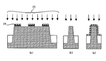
図2乃至図13及び図16乃至図24の各々において、(a)は各工程における図1のA−A’線断面を示す図、(b)は各工程におけるB−B’線断面を示す図、及び(c)は各工程におけるC−C’線断面を示す図である。即ち、図2乃至図13及び図16乃至図24の各々において、(a)は活性領域13の長手方向縦断面図、(b)は活性領域のビット線用コンタクト部分の幅方向縦断面図、及び(c)は活性領域のチャネル部の幅方向縦断面図である。なお、以下の説明において、「幅」は、活性領域13に関する限り、平面図において(基板の表面側から見て、あるいは積層方向上方から見て)、長手方向に直交する方向の長さを意味する。
In each of FIGS. 2 to 13 and FIGS. 16 to 24, (a) is a diagram showing a cross section taken along line AA ′ of FIG. FIGS. 3A and 3C are cross-sectional views taken along the line CC ′ in each step. That is, in each of FIGS. 2 to 13 and FIGS. 16 to 24, (a) is a longitudinal sectional view in the longitudinal direction of the
以下、図2乃至図24を参照して、本実施の形態に係るDRAMの製造方法について説明する。 Hereinafter, a method of manufacturing a DRAM according to the present embodiment will be described with reference to FIGS.
まず、シリコン基板(図2の21)を用意し、その表面に第1のゲート絶縁膜(図2の22)(例えば、厚み13nm)を堆積させ、あるいは熱酸化により形成する。続いて、第1のゲート絶縁膜22の上にシリコン窒化膜(図2の23)(例えば、厚み120nm)を形成する。さらに、シリコン窒化膜23の上であって、活性領域(図1の13)に対応する位置に、公知のリソグラフィ技術を用いてレジストパターンを形成する。それから、レジストパターンをマスクとしてドライエッチングを行い、シリコン窒化膜23をエッチングし、その後、レジストパターンを除去する。このときの状態を図2(a),(b)及び(c)に示す。
First, a silicon substrate (21 in FIG. 2) is prepared, and a first gate insulating film (22 in FIG. 2) (for example, 13 nm in thickness) is deposited on the surface, or is formed by thermal oxidation. Subsequently, a silicon nitride film (23 in FIG. 2) (for example, a thickness of 120 nm) is formed on the first gate
次に、図3(a),(b)及び(c)に示すように、シリコン窒化膜23をマスクとして第1ゲート酸化膜22及びシリコン基板21を(例えば300nm)エッチングする。これにより、活性領域となる同一幅を持つフィン部が形成される。
Next, as shown in FIGS. 3A, 3B, and 3C, the first
次に、図4(a),(b)及び(c)に示すように、シリコン酸化膜24を(例えば350nm)堆積させ、その表面をシリコン窒化膜23の上面が露出するまでCMP(Chemical Mechanical Polish)法により研磨する。さらに、図5(a),(b)及び(c)に示すように、シリコン酸化膜24の一部(例えば、200nm厚)を異方性エッチング(エッチバック)する。
Next, as shown in FIGS. 4A, 4B, and 4C, a
次に、例えば燐酸を用いて、図6(a),(b)及び(c)に示すように、シリコン窒化膜23を除去する。
Next, the
次に、図7(a),(b)及び(c)に示すように、シリコン基板21の露出面を酸化させてシリコン酸化膜25(例えば、13nm厚)を形成する。この後、ウェル(Well)を形成するための不純物導入をイオン注入法により行なう。
Next, as shown in FIGS. 7A, 7B, and 7C, the exposed surface of the
次に、図8(a),(b)及び(c)に示すように、シリコン窒化膜26(例えば、30nm厚)を全面に堆積させる。 Next, as shown in FIGS. 8A, 8B, and 8C, a silicon nitride film 26 (for example, 30 nm thick) is deposited on the entire surface.
次に、図9(a),(b)及び(c)に示すように、公知のリソグラフィ技術により、FinFETのゲート電極形成領域及びダミーゲート形成領域が開口するように、レジストパターン27を形成する。レジストパターン27間のスペース(即ち、レジストパターン間の間隔)は、例えば45nmとする。
Next, as shown in FIGS. 9A, 9B, and 9C, a resist
続いて、図10(a),(b)及び(c)に示すように、レジストパターン27をエッチングマスクとして、シリコン窒化膜26をエッチングする。それから、ホトレジスト27を除去し、シリコン窒化膜26をマスクとして第1ゲート絶縁膜22と酸化膜25をエッチングし、図11(a),(b)及び(c)に示す状態とする。こうして、フィン部の表面を覆う第1ゲート絶縁膜22、酸化膜25及び窒化膜26のチャネル部に対応する部分に、選択的に開口が形成される。
Subsequently, as shown in FIGS. 10A, 10B, and 10C, the
次に、熱酸化により、図12(a),(b)及び(c)に示すように、酸化膜22、25及び窒化膜26に形成された開口内に露出する基板21の表面にのみ選択的に熱酸化膜28(例えば、10nm厚)を形成する。この結果、図12(b)に示すように、FinFETのチャネル部となる部分では、上面及び側面が熱酸化膜28で覆われる。一方、ビット線用コンタクト部(及びストレージノードコンタクト)となる領域は、図12(c)に示すようにシリコン窒化膜26で覆われているため、熱酸化膜28は形成されない。
Next, only the surface of the
次に、ケミカルドライエッチもしくは希釈したHF溶液により、図13(a),(b)及び(c)に示すように、熱酸化膜28を除去する。上述したように、活性領域のチャネル部となる部分には熱酸化膜28が形成されているが、ビット線用コンタクト部分及びストレージノードコンタクト部分には、熱酸化膜28は形成されていない。したがって、この熱酸化膜28の除去により、活性領域の幅が、チャネル部においてのみ選択的に縮小され、ビット線用コンタクト部分及びストレージノードコンタクト部分の幅よりも狭い構造となる。
Next, as shown in FIGS. 13A, 13B and 13C, the
図14は、熱酸化膜28を除去した後のフィン部の状態を示す平面図(活性領域が6個配列形成されている)である。図示のように、各活性領域13において、ストレージノードコンタクト部となる部分13−1の幅13−6及びビット線用コンタクト部となる部分13−3の幅13−5が、FinFETのチャネル部となる部分13−2の幅13−4よりも広い。なお、ゲート電極は、後に図15に示すように形成される。
FIG. 14 is a plan view showing the state of the fin portion after removing the thermal oxide film 28 (in which six active regions are arranged). As shown in the figure, in each
熱酸化膜28を除去した後、図16(a),(b)及び(c)に示すように、イオン注入によりシリコン窒化膜26で覆われていない領域(チャネル部)にのみに不純物29を注入する。この不純物は、例えば、B(ボロン)であって、その濃度は、1E12cm−3とする。
After removing the
次に、、図17(a),(b)及び(c)に示すように、シリコン窒化膜26をケミカルドライエッチもしくは希釈したHF溶液により除去する。
Next, as shown in FIGS. 17A, 17B, and 17C, the
次に、図18(a),(b)及び(c)に示すように、基板21の露出面を酸化することによりゲート酸化膜30(例えば、6nm厚)を形成する。さらに、ゲート酸化膜30に対して、プラズマによる窒化処理を行なってその表面を酸窒化膜(例えば、厚み3nm)とする。なお、ゲート酸化膜30及び酸窒化膜に代えて、HTO(High Temperature Oxide)や高誘電率膜を用いてもよい。
Next, as shown in FIGS. 18A, 18B, and 18C, the exposed surface of the
次に、図19(a),(b)及び(c)に示すように、ゲート電極用のポリシリコン31を形成し、その表面を平坦化する(例えば、第1ゲート絶縁膜22上で厚み60nm)。続いて、タングステンシリサイド(WSi)(例えば、5nm厚)、タングステン窒化膜(例えば、10nm厚)及びタングステン(例えば、100nm厚)からなる積層膜32と、シリコン窒化膜33(例えば、100nm厚)とを順次堆積させる。
Next, as shown in FIGS. 19A, 19B, and 19C, the
次に、公知のリソグラフィ技術を用い、図20(a),(b)及び(c)に示すように、シリコン窒化膜33の表面であって、ゲート電極領域及びダミーゲート領域に対応する部分にレジストパターン34を形成する。このときレジストパターン34間のスペースは、例えば55nmとする。
Next, using a known lithographic technique, as shown in FIGS. 20A, 20B, and 20C, the surface of the
次に、レジストパターン34をマスクとして、図21(a),(b)及び(c)に示すように、シリコン窒化膜33をエッチングし、その後、レジストパターン34を除去する。
Next, using the resist
次に、図22(a),(b)及び(c)に示すように、残ったシリコン窒化膜33をマスクとして、タングステン、タングステン窒化膜及びタングステンシリサイドからなる積層膜32をエッチングする。
Next, as shown in FIGS. 22A, 22B and 22C, the
次に、シリコン窒化膜(例えば、15nm厚)を堆積させ、ドライエッチングによりエッチバックし、図23(a),(b)及び(c)に示すように、サイドウォール35を形成する。 Next, a silicon nitride film (for example, 15 nm thick) is deposited and etched back by dry etching to form sidewalls 35 as shown in FIGS. 23 (a), 23 (b), and 23 (c).
次に、図24(a),(b)及び(c)に示すように、シリコン窒化膜33及びサイドウォール35をマスクとして、ポリシリコン31をエッチングする。
Next, as shown in FIGS. 24A, 24B and 24C, the
この後、公知のDRAMプロセスにより、キャパシタの形成や配線の形成を行なってDRAMが完成する。 Thereafter, capacitors are formed and wirings are formed by a known DRAM process to complete the DRAM.
以上のようにして、本実施の形態によれば、活性領域において、チャネル部の幅よりもストレージノードコンタクト部分の幅及びビット線用コンタクト部分の幅が広いFinFETを含む半導体装置(DRAM)を製造することができる。これにより、チャネル部を完全空乏化するために必要な幅(例えば30nm)にまで縮小しても、ストレージノードコンタクト部分及びビット線用コンタクト部分においては十分な幅(例えば、50nm)を確保することができ、コンタクト抵抗の上昇を抑えることができる。即ち、本実施の形態により、チャネル部を完全空乏化した上で、十分なオン電流が得られるFinFETを含む半導体装置(ツインセル構造のDRAM)が得られる。 As described above, according to the present embodiment, a semiconductor device (DRAM) including a FinFET in which the width of the storage node contact portion and the width of the bit line contact portion are wider than the width of the channel portion in the active region is manufactured. can do. As a result, even when the channel portion is reduced to a width (for example, 30 nm) necessary for fully depleting the channel portion, a sufficient width (for example, 50 nm) is secured in the storage node contact portion and the bit line contact portion. And increase in contact resistance can be suppressed. In other words, according to the present embodiment, a semiconductor device (a twin cell structure DRAM) including a FinFET that can obtain a sufficient on-current after the channel portion is completely depleted can be obtained.
また、本実施の形態によれば、従来に比べて増加する工程がわずかであるので、製造コストをほとんど上昇させることなく、上記構造のDRAMを製造することができる。 In addition, according to the present embodiment, since the number of steps increased compared to the conventional method is small, the DRAM having the above structure can be manufactured with almost no increase in manufacturing cost.
次に、図25乃至図39を参照して、本発明の第2の実施の形態について説明する。 Next, a second embodiment of the present invention will be described with reference to FIGS.
まず、第1の実施の形態と同様の工程(図2乃至図8)を行い、図8に示す状態とする。 First, steps similar to those in the first embodiment (FIGS. 2 to 8) are performed to obtain the state shown in FIG.
この後、図25(a)、(b)及び(c)に示すように、シリコン酸化膜51(例えば、100nm厚)を全面に堆積させ、CMP法により例えば20nm研磨して表面を平滑化する。 Thereafter, as shown in FIGS. 25A, 25B, and 25C, a silicon oxide film 51 (eg, 100 nm thick) is deposited on the entire surface, and polished by, eg, 20 nm by CMP to smooth the surface. .
次に、公知のリソグラフィ技術により、図26(a)、(b)及び(c)に示すように、FinFETのゲート電極領域及びダミーゲート領域上が開口するレジストパターン52を形成する。このときレジストパターン52間のスペースは、例えば45nmとする。
Next, as shown in FIGS. 26A, 26B, and 26C, a resist
次に、図27(a)、(b)及び(c)に示すように、レジストパターン52をマスクとしてシリコン酸化膜51をエッチングする。その後、図28(a)、(b)及び(c)に示すように、レジストパターン52を除去する。
Next, as shown in FIGS. 27A, 27B, and 27C, the
次に、図29(a)、(b)及び(c)に示すように、シリコン酸化膜51をエッチングマスクとして、シリコン窒化膜26を異方性エッチングする。
Next, as shown in FIGS. 29A, 29B and 29C, the
次に、図30(a)、(b)及び(c)に示すように、シリコン窒化膜53(例えば、10nm厚)を堆積させる。それから、シリコン窒化膜53を異方性エッチングし、図31(a)、(b)及び(c)に示すように、シリコン酸化膜51の側壁にシリコン窒化膜53からなるサイドウォール54を形成する。このとき、第1ゲート絶縁膜22の一部、シリコン酸化膜25もエッチングされる。こうして、フィン部に形成された、第1ゲート絶縁膜22、シリコン酸化膜25及びシリコン窒化膜53に開口が形成される。
Next, as shown in FIGS. 30A, 30B, and 30C, a silicon nitride film 53 (for example, 10 nm thick) is deposited. Then, the
次に、熱酸化により、開口に露出するシリコン基板21の露出面を選択的に酸化し、図32(a)、(b)及び(c)に示すように、シリコン酸化膜55(例えば、10nm厚)を形成する。
Next, the exposed surface of the
次に、ケミカルドライエッチもしくは希釈したHF溶液により、図33(a)、(b)及び(c)に示すように、シリコン酸化膜55を除去する。これにより、第1の実施の形態と同様、活性領域のチャネル部の幅を、選択的に、ストレージノードコンタクト部分の幅及びビット線用コンタクト部分の幅よりも狭くすることができる。
Next, as shown in FIGS. 33A, 33B and 33C, the
次に、図34(a)、(b)及び(c)に示すように、シリコン基板21の露出面を酸化してゲート酸化膜56(例えば、6nm厚)を形成する。それから、プラズマを用いた窒化処理により、ゲート酸化膜56の表面を窒化処理し、酸窒化膜(例えば、3nm厚)を形成する。なお、ゲート酸化膜56及び酸窒化膜に代えて、HTOや高誘電率膜を用いてもよい。
Next, as shown in FIGS. 34A, 34B, and 34C, the exposed surface of the
次に、図35(a)、(b)及び(c)に示すように、ゲート電極用のポリシリコン57を、例えば40nm以上(一例として100nm)の厚さとなるよう堆積させる。なお、ポリシリコン57は、ボロンが、例えば、濃度2E20cm−3以上(in-situ)となるようにドープされているものが望ましい。
Next, as shown in FIGS. 35A, 35B, and 35C,
次に、図36(a)、(b)及び(c)に示すように、シリコン酸化膜51が露出するまでCMP法によりゲート酸化膜用ポリシリコン57を研磨する。
Next, as shown in FIGS. 36A, 36B and 36C, the gate
次に、図37(a)、(b)及び(c)に示すように、タングステンシリサイド(例えば、5nm厚)、タングステン窒化膜(例えば、10nm厚)及びタングステン(例えば、55nm厚)からなる積層膜58を形成する。また、積層膜58の上にシリコン窒化膜59(例えば、100nm厚)を堆積させる。さらに、公知のリソグラフィ技術により、シリコン窒化膜59の上であって、ゲート電極領域及びダミーゲート領域に対応する部分に、レジストパターン60を形成する。
Next, as shown in FIGS. 37A, 37B, and 37C, a stack of tungsten silicide (for example, 5 nm thick), tungsten nitride film (for example, 10 nm thick), and tungsten (for example, 55 nm thick). A
次に、図38(a)、(b)及び(c)に示すように、ホトレジスト60をエッチングマスクとしてシリコン窒化膜59をエッチングし、その後、ホトレジスト60を除去する。
Next, as shown in FIGS. 38A, 38B, and 38C, the
次に、図39(a)、(b)及び(c)に示すように、シリコン窒化膜59をマスクとして、タングステン、タングステン窒化膜及びタングステンシリサイドからなる積層膜58をドライエッチングする。
Next, as shown in FIGS. 39A, 39B and 39C, the
この後、公知のDRAMプロセスにより、キャパシタの形成や配線の形成を行なってDRAMが完成する。 Thereafter, capacitors are formed and wirings are formed by a known DRAM process to complete the DRAM.
以上のようにし、本実施の形態においても第1の実施の形態と同様に、活性領域において、チャネル部の幅よりもストレージノードコンタクト部分の幅及びビット線用コンタクト部分の幅が広いFinFETを含む半導体装置(DRAM)を製造することができる。これにより、チャネル部の幅を縮小し完全空乏化した上で、十分なオン電流が得られるFinFETを含む半導体装置が得られる。また、製造コストの上昇もほとんどない。 As described above, the present embodiment also includes FinFETs in which the width of the storage node contact portion and the width of the bit line contact portion are wider than the width of the channel portion in the active region, as in the first embodiment. A semiconductor device (DRAM) can be manufactured. As a result, a semiconductor device including a FinFET that can obtain a sufficient on-current while reducing the width of the channel portion to be completely depleted can be obtained. Moreover, there is almost no increase in manufacturing cost.
次に図40乃至図57を参照して、本発明の第3の実施の形態について説明する。 Next, a third embodiment of the present invention will be described with reference to FIGS.
まず、第1の実施の形態と同様の工程(図2乃至図8)を行い、図8に示す状態とする。 First, steps similar to those in the first embodiment (FIGS. 2 to 8) are performed to obtain the state shown in FIG.
この後、図40(a)、(b)及び(c)に示すように、シリコン酸化膜71(例えば、膜厚200)を形成し、CMP法により表面を研磨(例えば、厚さ20nm)して平滑化する。 Thereafter, as shown in FIGS. 40A, 40B, and 40C, a silicon oxide film 71 (for example, a film thickness of 200) is formed, and the surface is polished by a CMP method (for example, a thickness of 20 nm). To smooth.
次に、図41(a)、(b)及び(c)に示すように、公知のリソグラフィ技術により、FinFETのゲート電極領域及びダミーゲート領域が開口するようにレジストパターン72を形成する。このときのレジストパターン72間のスペースは、例えば、45nmとする。
Next, as shown in FIGS. 41A, 41B, and 41C, a resist
次に、図42(a)、(b)及び(c)に示すように、レジストパターン72をマスクとしてシリコン酸化膜71をエッチングする。その後、図43(a)、(b)及び(c)に示すように、レジストパターン72を除去する。
Next, as shown in FIGS. 42A, 42B, and 42C, the
次に、図44(a)、(b)及び(c)に示すように、シリコン酸化膜71をエッチングマスクとしてシリコン窒化膜26を異方性エッチングする。
Next, as shown in FIGS. 44A, 44B and 44C, the
次に、図45(a)、(b)及び(c)に示すように、全面にシリコン窒化膜73(例えば、10nm厚)を堆積させる。それから、シリコン窒化膜73を異方性エッチングし、図46(a)、(b)及び(c)に示すように、シリコン酸化膜71の側壁にシリコン窒化膜73からなるサイドウォール74を形成する。このとき、第1ゲート絶縁膜22の一部及びシリコン酸化膜25も除去される。こうして、フィン部の表面を覆う第1ゲート絶縁膜22、酸化膜25及び窒化膜73のチャネル部に対応する部分に、選択的に開口が形成される。
Next, as shown in FIGS. 45A, 45B and 45C, a silicon nitride film 73 (for example, 10 nm thick) is deposited on the entire surface. Then, the
次に、熱酸化により、図47(a)、(b)及び(c)に示すように、シリコン基板21の露出面に熱酸化膜75(例えば、10nm厚)を形成する。
Next, as shown in FIGS. 47A, 47B, and 47C, a thermal oxide film 75 (for example, 10 nm thick) is formed on the exposed surface of the
次に、ケミカルドライエッチもしくは希釈したHF溶液により、図48(a)、(b)及び(c)に示すように、熱酸化膜75を除去する。これにより、活性領域のチャネル部の幅を、選択的に、ストレージノードコンタクト部分の幅及びビット線用コンタクト部分の幅よりも狭くすることができる。 Next, the thermal oxide film 75 is removed by chemical dry etching or diluted HF solution as shown in FIGS. Thereby, the width of the channel portion of the active region can be selectively made smaller than the width of the storage node contact portion and the width of the bit line contact portion.
次に、図49(a)、(b)及び(c)に示すように、開口内に露出したシリコン基板21の露出面を酸化することによりゲート酸化膜76(例えば、6nm厚)を形成し、その表面をプラズマによる窒素処理により酸窒化膜(例えば、3nm厚)とする。なお、ゲート酸化膜76及び酸窒化膜に代えて、HTOや高誘電率膜を用いてもよい。
Next, as shown in FIGS. 49A, 49B and 49C, a gate oxide film 76 (for example, 6 nm thick) is formed by oxidizing the exposed surface of the
次に、図50(a)、(b)及び(c)に示すように、ゲート電極用のポリシリコン77(例えば、100nm厚)を堆積させる。ここで、ポリシリコン77としては、例えば、ボロン(B)が、濃度2E20cm−3以上(in-situ)となるようにドープされているものが望ましい。
Next, as shown in FIGS. 50A, 50B, and 50C,
次に、ゲート電極形成領域上のポリシリコン77が所定の厚さ、例えば50nm、となるようにドライエッチバックする。それから、図51(a)、(b)及び(c)に示すように、タングステンシリサイド(例えば、5nm厚)、タングステン窒化膜(例えば、10nm厚)及びタングステン(例えば、55nm厚)からなる積層膜78を形成する。
Next, dry etching back is performed so that the
次に、図52(a)、(b)及び(c)に示すように、ゲート電極形成領域において厚さが、例えば60nmとなるように、積層膜78をドライエッチバックする。
Next, as shown in FIGS. 52A, 52B, and 52C, the
次に、図53(a)、(b)及び(c)に示すように、シリコン窒化膜79(例えば、100nm厚)を堆積させる。それから、図54(a)、(b)及び(c)に示すように、シリコン酸化膜71が露出するまで、CMP法によりシリコン窒化膜79を研磨する。
Next, as shown in FIGS. 53A, 53B, and 53C, a silicon nitride film 79 (for example, 100 nm thick) is deposited. Then, as shown in FIGS. 54A, 54B and 54C, the
次に、公知のリソグラフィ技術により、図55(a)、(b)及び(c)に示すように基板コンタクトに対応する部分(即ち、ストレージノードコンタクト部分及びビット線用コンタクト部分、図69参照。)が開口するように、レジストパターン80を形成する。
Next, as shown in FIGS. 55A, 55B, and 55C, a portion corresponding to the substrate contact (that is, a storage node contact portion and a bit line contact portion, see FIG. 69) by a known lithography technique. The resist
次に、図56(a)、(b)及び(c)に示すように、レジストパターン80をマスクとしてシリコン酸化膜71を異方性ドライエッチングする。このとき、シリコン酸化膜71をエッチングする際のシリコン窒化膜に対する選択比は15以上が望ましい。レジストパターン80の開口内のシリコン酸化膜71を除去した後、異方性ドライエッチングを引き続き行うことにより、シリコン窒化膜26及び第1ゲート絶縁膜22を除去してシリコン基板21の表面を露出させる。
Next, as shown in FIGS. 56A, 56B, and 56C, the
次に、ホトレジスト80を除去した後、図57(a)、(b)及び(c)に示すように、ポリシリコン81を例えば200nm堆積させ、エッチバックしてシリコン窒化膜79を露出させる。なお、ポリシリコン81は、例えばリン(P)を1E20cm−3の濃度(in-situ)でドープしたものである。
Next, after removing the
この後、公知のDRAMプロセスにより、キャパシタの形成や配線の形成を行なってDRAMが完成する。 Thereafter, capacitors are formed and wirings are formed by a known DRAM process to complete the DRAM.
以上のようにし、本実施の形態においても第1、第2の実施の形態と同様に、活性領域において、チャネル部の幅よりもストレージノードコンタクト部分の幅及びビット線用コンタクト部分の幅が広いFinFETを含む半導体装置(DRAM)を製造することができる。これにより、チャネル部の幅を縮小し完全空乏化した上で、十分なオン電流が得られるFinFETを含む半導体装置が得られる。また、製造コストの上昇もほとんどない。 As described above, also in this embodiment, as in the first and second embodiments, in the active region, the width of the storage node contact portion and the width of the bit line contact portion are wider than the width of the channel portion. A semiconductor device (DRAM) including a FinFET can be manufactured. As a result, a semiconductor device including a FinFET that can obtain a sufficient on-current while reducing the width of the channel portion to be completely depleted can be obtained. Moreover, there is almost no increase in manufacturing cost.
次に、図58乃至図68を参照して、本発明の第4の実施の形態について説明する。 Next, a fourth embodiment of the present invention will be described with reference to FIGS.
まず、第2の実施の形態と同様の工程(図2乃至図8、図25及び図26)を行い、図26示す状態とする。 First, steps similar to those of the second embodiment (FIGS. 2 to 8, FIG. 25, and FIG. 26) are performed to obtain the state shown in FIG.
この後、RELACS(Resist Enhancement Lithography Assisted by Chemical Shrink)法により、図58(a)、(b)及び(c)に示すに示すように、レジストパターン52の側壁にサイドウォール91(例えば、10nm厚)を形成する。なお、サイドウォール91は、後に形成されるチャネルの長さ(図58(a)の左右方向長さ)を短くするためのものである。このサイドウォール91の形成に代えて、レジストパターン52をマスクとしてシリコン酸化膜51をエッチングし、ホトレジスト52を除去した後、シリコン酸化膜51の側壁に酸化膜やシリコン窒化膜によるサイドウォールを形成しても同様の効果が得られる。
Thereafter, a sidewall 91 (for example, 10 nm thick) is formed on the sidewall of the resist
次に、ホトレジスト52及びサイドウォール91をマスクとして、図59(a)、(b)及び(c)に示すに示すように、シリコン酸化膜51を異方性エッチングする。それから、図60(a)、(b)及び(c)に示すに示すように、ホトレジスト52及びサイドウォール91を除去する。
Next, using the
次に、熱燐酸等を用い、図61(a)、(b)及び(c)に示すように、シリコン窒化膜26を、例えば30nm以上、等方性エッチングする。それから、図62(a)、(b)及び(c)に示すように、開口内の第1ゲート酸化膜22およびシリコン酸化膜25を除去する。こうして、フィン部の表面を覆う第1ゲート絶縁膜22、酸化膜25及び窒化膜26のチャネル部に対応する部分に、選択的に開口が形成される。さらに、開口内に露出した基板シリコン21を、例えば10nm、等方性エッチングする。これにより活性領域におけるチャネル部の幅がストレージノードコンタクト部分及びビット専用コンタクト部分の幅よりも狭い構造となる。
Next, as shown in FIGS. 61A, 61B and 61C, the
次に、図63(a)、(b)及び(c)に示すように、シリコン基板21の露出面に、熱酸化によりゲート酸化膜92(例えば、6nm厚)を形成する。この後、ゲート酸化膜92に対してプラズマによる窒素処理を行って酸窒化膜(例えば、3nm厚)を形成する。なお、ゲート酸化膜92及び酸窒化膜に代えて、HTOや高誘電率膜を用いてもよい。
Next, as shown in FIGS. 63A, 63B, and 63C, a gate oxide film 92 (for example, 6 nm thick) is formed on the exposed surface of the
次に、図64(a)、(b)及び(c)に示すように、ゲート電極用のポリシリコン93(例えば、100nm厚)堆積させる。ポリシリコン93としては、例えば、ボロン(B)が濃度2E20cm−3以上(in-situ)でドープされているものが望ましい。
Next, as shown in FIGS. 64A, 64B, and 64C,
次に、CMP法により、図65(a)、(b)及び(c)に示すように、シリコン酸化膜51が露出するまで、ポリシリコン93を研磨する。
Next, as shown in FIGS. 65A, 65B, and 65C, the
次に、図66(a)、(b)及び(c)に示すように、タングステンシリサイド(例えば、5nm厚)、タングステン窒化膜(例えば、10nm厚)及びタングステン(例えば、55nm)からなる積層膜94と、シリコン窒化膜95(例えば、100nm厚)とを堆積させる。さらに、シリコン窒化膜95上であって、ゲート電極領域及びダミーゲート領域に対応する部分に、公知のリソグラフィ技術により、レジストパターン96を形成する。
Next, as shown in FIGS. 66A, 66B and 66C, a laminated film made of tungsten silicide (for example, 5 nm thick), tungsten nitride film (for example, 10 nm thick) and tungsten (for example, 55 nm). 94 and a silicon nitride film 95 (for example, 100 nm thick) are deposited. Further, a resist pattern 96 is formed on the
次に、図67(a)、(b)及び(c)に示すように、レジストパターン96をマスクとしてシリコン窒化膜95をエッチングし、その後、ホトレジスト96を除去する。
Next, as shown in FIGS. 67A, 67B, and 67C, the
次に、図68(a)、(b)及び(c)に示すように、シリコン窒化膜95をマスクとして、タングステン、タングステン窒化膜およびタングステンシリサイドからなる積層膜94をエッチングする。
Next, as shown in FIGS. 68A, 68B and 68C, the
この後、公知のDRAMプロセスにより、キャパシタの形成や配線の形成を行なってDRAMが完成する。 Thereafter, capacitors are formed and wirings are formed by a known DRAM process to complete the DRAM.
以上のようにし、本実施の形態においても第1乃至第3の実施の形態と同様に、活性領域において、チャネル部の幅よりもストレージノードコンタクト部分の幅及びビット線用コンタクト部分の幅が広いFinFETを含む半導体装置(DRAM)を製造することができる。これにより、チャネル部の幅を縮小し完全空乏化した上で、十分なオン電流が得られるFinFETを含む半導体装置が得られる。また、製造コストの上昇もほとんどない。 As described above, also in the present embodiment, as in the first to third embodiments, the width of the storage node contact portion and the width of the bit line contact portion are wider than the width of the channel portion in the active region. A semiconductor device (DRAM) including a FinFET can be manufactured. As a result, a semiconductor device including a FinFET that can obtain a sufficient on-current while reducing the width of the channel portion to be completely depleted can be obtained. Moreover, there is almost no increase in manufacturing cost.
上述した第1乃至第4の実施の形態に係る半導体装置の製造方法は、全て、6F2メモリセル構造のDRAMに適用することができる。6F2メモリセル構造の平面レイアウトを図69に示す。 The method of manufacturing a semiconductor device according to the first to fourth embodiments described above can all be applied to a DRAM of 6F 2 memory cell structure. 6F 2 shows a planar layout of a memory cell structure in FIG. 69.
図69において、トランスファーゲート101は、所定の周期(ピッチ=2F、F:Feature size)で互いに平行かつ上下方向に伸びるように配置されている。トラスファーゲート101の両側壁にはLDDサイドウォール102が形成されている。活性領域103は、互いに隣り合う2本のトランスファーゲート101が横切るように配列形成される。また、活性領域103は、トランスファーゲートと直交する方向に関しては、一本のダミーゲートを挟んで隣り合うように配列形成されている。活性領域103の上方(図の表面側)には、ストレージノードコンタクト部及びビット線用コンタクト部に接続される基板コンタクト104が形成されている。ビット線105は、概ね、トランスファーゲート101と直交する方向に沿って、所定の間隔(ピッチ=2F)で形成されている。具体的には、ビット線105は、ビット線用コンタクト部の上を通過し、ストレージノードコンタクト部の上を避けるように形成されている。トランスファーゲート101、活性領域103及びビット線105の配置は、図に破線で示す2F×3F=6F2の基本領域の構造パターンを繰り返すパターンとなるようになされている。
In FIG. 69, the
以上、本発明についていくつかの実施の形態に即して説明したが、本発明はこれら実施の形態に限定されるものではなく、本願発明の主旨から逸脱することなく種々の変形が可能である。例えば、DRAMのみならず、他の半導体装置にも適用できる。 As mentioned above, although this invention was demonstrated according to some embodiment, this invention is not limited to these embodiment, A various deformation | transformation is possible without deviating from the main point of this invention. . For example, the present invention can be applied not only to a DRAM but also to other semiconductor devices.
11,12 ゲート電極領域
13 活性領域
13−1 ストレージノードコンタクト部となる部分
13−2 FinFETのチャネル部となる部分
13−3 ビット線用コンタクト部となる部分
13−4 FinFETのチャネル部となる部分の幅
13−5 ビット線用コンタクト部となる部分の幅
13−6 ストレージノードコンタクト部となる部分の幅
21 シリコン基板
22 第1のゲート絶縁膜
23 シリコン窒化膜
24 シリコン酸化膜
25 シリコン酸化膜
26 シリコン窒化膜
27 レジストパターン
28 熱酸化膜
29 不純物
30 ゲート酸化膜
31 ポリシリコン
32 積層膜
33 シリコン窒化膜
34 レジストパターン
35 サイドウォール
51 シリコン酸化膜
52 レジストパターン
53 シリコン窒化膜
54 サイドウォール
55 シリコン酸化膜
56 ゲート酸化膜
57 ポリシリコン
58 積層膜
59 シリコン窒化膜
60 レジストパターン
71 シリコン酸化膜
72 レジストパターン
73 シリコン窒化膜
74 サイドウォール
75 熱酸化膜
76 ゲート酸化膜
77 ポリシリコン
78 積層膜
79 シリコン窒化膜
80 レジストパターン
81 ポリシリコン
91 サイドウォール
92 ゲート酸化膜
93 ポリシリコン
94 積層膜
95 シリコン窒化膜
96 レジストパターン
101 トランスファーゲート
102 LDDサイドウォール
103 活性領域
104 基板コンタクト
105 ビット線
DESCRIPTION OF
Claims (9)
前記活性領域のチャネル部となる部分の幅が、ソース・ドレインとなる部分の幅よりも狭いことを特徴とする半導体装置。 In a semiconductor device having a fin-shaped active region,
A width of a portion to be a channel portion of the active region is narrower than a width of a portion to be a source / drain.
前記チャネル部が完全空乏化されていることを特徴とする半導体装置。 The semiconductor device according to claim 1,
A semiconductor device, wherein the channel portion is fully depleted.
一つの前記活性領域に二つのチャネル部が形成されていることを特徴とする半導体装置。 The semiconductor device according to claim 1 or 2,
2. A semiconductor device, wherein two channel portions are formed in one active region.
前記活性領域を複数有し、当該複数の活性領域が配列形成されていることを特徴とする半導体装置。 The semiconductor device according to claim 1, 2, or 3,
A semiconductor device comprising a plurality of the active regions, wherein the plurality of active regions are arranged.
前記活性領域がDRAMのセルトランジスタに用いられていることを特徴とする半導体装置。 The semiconductor device according to claim 4,
A semiconductor device, wherein the active region is used for a cell transistor of a DRAM.
前記セルトランジスタが、6F2レイアウト構造で配列形成されていることを特徴とする半導体装置。 The semiconductor device according to claim 5,
Wherein a said cell transistors are arranged and formed in 6F 2 layout structure.
前記活性領域となる一定幅のフィン部を形成するフィン部形成工程と、
前記フィン部のうちチャネル部となる部分の幅を部分的に縮小する縮小工程と、
を含むことを特徴とする半導体装置の製造方法。 In a method for manufacturing a semiconductor device having a fin-shaped active region,
A fin portion forming step for forming a fin portion having a constant width to be the active region;
A reduction step of partially reducing the width of the fin portion to become a channel portion;
A method for manufacturing a semiconductor device, comprising:
前記縮小工程が、
前記フィン部を覆う酸化膜及び窒化膜の前記チャネル部に対応する部分に選択的に開口を形成する工程と、
前記開口内に露出した前記フィン部の表面を選択的に酸化させて酸化膜を形成する工程と、
当該酸化膜を除去することにより、前記フィン部の幅を部分的に縮小する工程と、
を含むことを特徴とする半導体装置の製造方法。 In the manufacturing method of the semiconductor device according to claim 7,
The reduction step comprises:
Forming an opening selectively in a portion corresponding to the channel portion of the oxide film and the nitride film covering the fin portion;
Selectively oxidizing the surface of the fin portion exposed in the opening to form an oxide film;
A step of partially reducing the width of the fin portion by removing the oxide film;
A method for manufacturing a semiconductor device, comprising:
前記縮小工程が、
前記フィン部を覆う酸化膜及び窒化膜の、前記チャネル部に対応する部分に選択的に開口を形成する工程と、
前記開口内に露出した前記フィン部の表面を選択的にエッチングすることにより、前記フィン部の幅を部分的に縮小する工程と、
を含むことを特徴とする半導体装置の製造方法。 In the manufacturing method of the semiconductor device according to claim 7,
The reduction step comprises:
Selectively forming an opening in a portion corresponding to the channel portion of the oxide film and the nitride film covering the fin portion;
Selectively reducing the width of the fin portion by selectively etching the surface of the fin portion exposed in the opening;
A method for manufacturing a semiconductor device, comprising:
Priority Applications (2)
| Application Number | Priority Date | Filing Date | Title |
|---|---|---|---|
| JP2006297570A JP2008117838A (en) | 2006-11-01 | 2006-11-01 | Semiconductor device and manufacturing method thereof |
| US11/930,453 US20080099858A1 (en) | 2006-11-01 | 2007-10-31 | Semiconductor device and manfacturing method of the same |
Applications Claiming Priority (1)
| Application Number | Priority Date | Filing Date | Title |
|---|---|---|---|
| JP2006297570A JP2008117838A (en) | 2006-11-01 | 2006-11-01 | Semiconductor device and manufacturing method thereof |
Publications (1)
| Publication Number | Publication Date |
|---|---|
| JP2008117838A true JP2008117838A (en) | 2008-05-22 |
Family
ID=39329112
Family Applications (1)
| Application Number | Title | Priority Date | Filing Date |
|---|---|---|---|
| JP2006297570A Pending JP2008117838A (en) | 2006-11-01 | 2006-11-01 | Semiconductor device and manufacturing method thereof |
Country Status (2)
| Country | Link |
|---|---|
| US (1) | US20080099858A1 (en) |
| JP (1) | JP2008117838A (en) |
Cited By (5)
| Publication number | Priority date | Publication date | Assignee | Title |
|---|---|---|---|---|
| JP2010098081A (en) * | 2008-09-16 | 2010-04-30 | Hitachi Ltd | Semiconductor device |
| KR20110051168A (en) * | 2008-06-30 | 2011-05-17 | 어드밴스드 마이크로 디바이시즈, 인코포레이티드 | Double-gate and triple-gate transistors formed on bulk substrates and methods of forming these transistors |
| KR101445450B1 (en) * | 2012-07-03 | 2014-09-26 | 타이완 세미콘덕터 매뉴팩쳐링 컴퍼니 리미티드 | Multi-Gate FETs and Methods for Forming the Same |
| US9041115B2 (en) | 2012-05-03 | 2015-05-26 | Taiwan Semiconductor Manufacturing Company, Ltd. | Structure for FinFETs |
| KR20160107009A (en) * | 2015-03-03 | 2016-09-13 | 삼성전자주식회사 | Integrated circuit device |
Families Citing this family (7)
| Publication number | Priority date | Publication date | Assignee | Title |
|---|---|---|---|---|
| JP5602340B2 (en) * | 2007-10-30 | 2014-10-08 | ピーエスフォー ルクスコ エスエイアールエル | Semiconductor device and manufacturing method thereof |
| JP5569243B2 (en) | 2010-08-09 | 2014-08-13 | ソニー株式会社 | Semiconductor device and manufacturing method thereof |
| KR101797961B1 (en) * | 2011-06-09 | 2017-11-16 | 삼성전자주식회사 | Method for fabricating semiconductor device |
| US10515956B2 (en) | 2012-03-01 | 2019-12-24 | Taiwan Semiconductor Manufacturing Company | Semiconductor devices having Fin Field Effect Transistor (FinFET) structures and manufacturing and design methods thereof |
| US9105744B2 (en) * | 2012-03-01 | 2015-08-11 | Taiwan Semiconductor Manufacturing Company, Ltd. | Semiconductor devices having inactive fin field effect transistor (FinFET) structures and manufacturing and design methods thereof |
| KR102241974B1 (en) | 2014-09-23 | 2021-04-19 | 삼성전자주식회사 | Semiconductor devices and methods of manufacturing the same |
| CN107564953B (en) * | 2016-07-01 | 2021-07-30 | 中芯国际集成电路制造(上海)有限公司 | Varactor transistor and method of making the same |
Citations (6)
| Publication number | Priority date | Publication date | Assignee | Title |
|---|---|---|---|---|
| JPH06112309A (en) * | 1992-09-28 | 1994-04-22 | Fujitsu Ltd | Method for manufacturing semiconductor device |
| JP2002110963A (en) * | 2000-09-28 | 2002-04-12 | Toshiba Corp | Semiconductor device |
| JP2005086024A (en) * | 2003-09-09 | 2005-03-31 | Toshiba Corp | Semiconductor device and method for manufacturing same |
| JP2006522486A (en) * | 2003-04-03 | 2006-09-28 | アドバンスト・マイクロ・ディバイシズ・インコーポレイテッド | Method for forming a gate in a FinFET device and method for thinning fins in the channel region of the FinFET device |
| JP2007142392A (en) * | 2005-11-15 | 2007-06-07 | Internatl Business Mach Corp <Ibm> | Method, semiconductor structure (quasi self-aligned source / drain fin FET process) |
| JP2007294680A (en) * | 2006-04-25 | 2007-11-08 | Toshiba Corp | Semiconductor element, semiconductor device and manufacturing method thereof |
Family Cites Families (1)
| Publication number | Priority date | Publication date | Assignee | Title |
|---|---|---|---|---|
| KR100526889B1 (en) * | 2004-02-10 | 2005-11-09 | 삼성전자주식회사 | Fin field effect transistor structure |
-
2006
- 2006-11-01 JP JP2006297570A patent/JP2008117838A/en active Pending
-
2007
- 2007-10-31 US US11/930,453 patent/US20080099858A1/en not_active Abandoned
Patent Citations (6)
| Publication number | Priority date | Publication date | Assignee | Title |
|---|---|---|---|---|
| JPH06112309A (en) * | 1992-09-28 | 1994-04-22 | Fujitsu Ltd | Method for manufacturing semiconductor device |
| JP2002110963A (en) * | 2000-09-28 | 2002-04-12 | Toshiba Corp | Semiconductor device |
| JP2006522486A (en) * | 2003-04-03 | 2006-09-28 | アドバンスト・マイクロ・ディバイシズ・インコーポレイテッド | Method for forming a gate in a FinFET device and method for thinning fins in the channel region of the FinFET device |
| JP2005086024A (en) * | 2003-09-09 | 2005-03-31 | Toshiba Corp | Semiconductor device and method for manufacturing same |
| JP2007142392A (en) * | 2005-11-15 | 2007-06-07 | Internatl Business Mach Corp <Ibm> | Method, semiconductor structure (quasi self-aligned source / drain fin FET process) |
| JP2007294680A (en) * | 2006-04-25 | 2007-11-08 | Toshiba Corp | Semiconductor element, semiconductor device and manufacturing method thereof |
Cited By (15)
| Publication number | Priority date | Publication date | Assignee | Title |
|---|---|---|---|---|
| KR101630387B1 (en) | 2008-06-30 | 2016-06-24 | 어드밴스드 마이크로 디바이시즈, 인코포레이티드 | Double gate and tri-gate transistor formed on a bulk substrate and method for forming the transistor |
| KR20110051168A (en) * | 2008-06-30 | 2011-05-17 | 어드밴스드 마이크로 디바이시즈, 인코포레이티드 | Double-gate and triple-gate transistors formed on bulk substrates and methods of forming these transistors |
| JP2011527103A (en) * | 2008-06-30 | 2011-10-20 | アドバンスト・マイクロ・ディバイシズ・インコーポレイテッド | Double-gate and tri-gate transistors formed on a bulk substrate and method for forming the transistors |
| JP2010098081A (en) * | 2008-09-16 | 2010-04-30 | Hitachi Ltd | Semiconductor device |
| US9502419B2 (en) | 2012-05-03 | 2016-11-22 | Taiwan Semiconductor Manufacturing Company, Ltd. | Structure for FinFETs |
| US9041115B2 (en) | 2012-05-03 | 2015-05-26 | Taiwan Semiconductor Manufacturing Company, Ltd. | Structure for FinFETs |
| KR101531795B1 (en) * | 2012-05-03 | 2015-06-25 | 타이완 세미콘덕터 매뉴팩쳐링 컴퍼니 리미티드 | Structure for FinFETs |
| US9831253B2 (en) | 2012-05-03 | 2017-11-28 | Taiwan Semiconductor Manufacturing Company, Ltd. | FinFET memory device |
| US8883570B2 (en) | 2012-07-03 | 2014-11-11 | Taiwan Semiconductor Manufacturing Company, Ltd. | Multi-gate FETs and methods for forming the same |
| KR101445450B1 (en) * | 2012-07-03 | 2014-09-26 | 타이완 세미콘덕터 매뉴팩쳐링 컴퍼니 리미티드 | Multi-Gate FETs and Methods for Forming the Same |
| US9508714B2 (en) | 2012-07-03 | 2016-11-29 | Taiwan Semiconductor Manufacturing Company, Ltd. | Multi-gate FETs and methods for forming the same |
| US10103025B2 (en) | 2012-07-03 | 2018-10-16 | Taiwan Semiconductor Manufacturing Company, Ltd. | Multi-gate FETs and methods for forming the same |
| US10269568B2 (en) | 2012-07-03 | 2019-04-23 | Taiwan Semiconductor Manufacturing Company, Ltd. | Multi-gate FETs and methods for forming the same |
| KR20160107009A (en) * | 2015-03-03 | 2016-09-13 | 삼성전자주식회사 | Integrated circuit device |
| KR102327143B1 (en) | 2015-03-03 | 2021-11-16 | 삼성전자주식회사 | Integrated circuit device |
Also Published As
| Publication number | Publication date |
|---|---|
| US20080099858A1 (en) | 2008-05-01 |
Similar Documents
| Publication | Publication Date | Title |
|---|---|---|
| US7026688B2 (en) | Field effect transistors having multiple stacked channels | |
| US7229884B2 (en) | Phosphorous doping methods of manufacturing field effect transistors having multiple stacked channels | |
| US7648883B2 (en) | Phosphorous doping methods of manufacturing field effect transistors having multiple stacked channels | |
| US6992358B2 (en) | Semiconductor device and method for manufacturing the same | |
| US7323375B2 (en) | Fin field effect transistor device and method of fabricating the same | |
| CN101401196B (en) | Vertical EEPROM device | |
| US20080099858A1 (en) | Semiconductor device and manfacturing method of the same | |
| US20070284583A1 (en) | Semiconductor device and method of manufacturing the same | |
| US7829959B2 (en) | Semiconductor devices having line type active regions and methods of fabricating the same | |
| JP2002118255A (en) | Semiconductor device and manufacturing method thereof | |
| JP4530552B2 (en) | Semiconductor device and manufacturing method thereof | |
| JP2013143423A (en) | Semiconductor device and method of manufacturing the same | |
| JP2000332242A (en) | Semiconductor device and manufacturing method thereof | |
| US7745290B2 (en) | Methods of fabricating semiconductor device including fin-fet | |
| JP2004228571A (en) | SONOS nonvolatile memory and method of manufacturing the same | |
| US7579656B2 (en) | Transistor structure for semiconductor device and method of fabricating the same | |
| JP5555408B2 (en) | Semiconductor device manufacturing method and semiconductor device | |
| JP4527552B2 (en) | Semiconductor device and manufacturing method thereof | |
| JP2001332638A (en) | Manufacturing method of semiconductor memory device | |
| US7351625B2 (en) | Recessed transistors and methods of forming the same | |
| JPH1050953A (en) | Method for manufacturing semiconductor integrated circuit device | |
| JP2009231452A (en) | Semiconductor device and method of manufacturing the same |
Legal Events
| Date | Code | Title | Description |
|---|---|---|---|
| A977 | Report on retrieval |
Free format text: JAPANESE INTERMEDIATE CODE: A971007 Effective date: 20081017 |
|
| A131 | Notification of reasons for refusal |
Free format text: JAPANESE INTERMEDIATE CODE: A131 Effective date: 20081029 |
|
| A521 | Request for written amendment filed |
Free format text: JAPANESE INTERMEDIATE CODE: A523 Effective date: 20081224 |
|
| A131 | Notification of reasons for refusal |
Free format text: JAPANESE INTERMEDIATE CODE: A131 Effective date: 20091209 |
|
| A02 | Decision of refusal |
Free format text: JAPANESE INTERMEDIATE CODE: A02 Effective date: 20100407 |