JP2008084205A - CAD data processing program - Google Patents
CAD data processing program Download PDFInfo
- Publication number
- JP2008084205A JP2008084205A JP2006265881A JP2006265881A JP2008084205A JP 2008084205 A JP2008084205 A JP 2008084205A JP 2006265881 A JP2006265881 A JP 2006265881A JP 2006265881 A JP2006265881 A JP 2006265881A JP 2008084205 A JP2008084205 A JP 2008084205A
- Authority
- JP
- Japan
- Prior art keywords
- cad data
- association
- component
- data
- information
- Prior art date
- Legal status (The legal status is an assumption and is not a legal conclusion. Google has not performed a legal analysis and makes no representation as to the accuracy of the status listed.)
- Withdrawn
Links
Images




Classifications
-
- G—PHYSICS
- G06—COMPUTING OR CALCULATING; COUNTING
- G06F—ELECTRIC DIGITAL DATA PROCESSING
- G06F30/00—Computer-aided design [CAD]
- G06F30/30—Circuit design
- G06F30/39—Circuit design at the physical level
Landscapes
- Engineering & Computer Science (AREA)
- Computer Hardware Design (AREA)
- Physics & Mathematics (AREA)
- Theoretical Computer Science (AREA)
- Evolutionary Computation (AREA)
- Geometry (AREA)
- General Engineering & Computer Science (AREA)
- General Physics & Mathematics (AREA)
- Design And Manufacture Of Integrated Circuits (AREA)
Abstract
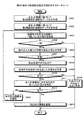
【課題】異なるCADによって作成されたCADデータに含まれる回路のシンボル名称やネットが完全に一致していない場合にでも、適切にCADデータを対応付けること。
【解決手段】CADデータ処理装置100は、入力部110から正ネット情報140aと逆ネット情報140bとを取得して記憶部140に記憶させ、対応付け処理部150aが、正ネット情報140aおよび逆ネット情報140bに含まれる部品に備えられた端子の特徴を基にして正ネット情報140aに含まれる部品、端子およびネットと逆ネット情報140bに含まれる部品、端子およびネットを対応付けた対応情報テーブル140jを作成する。
【選択図】 図1Even when circuit symbol names and nets included in CAD data created by different CADs do not completely match, CAD data is appropriately associated.
A CAD data processing apparatus 100 acquires normal net information 140a and reverse net information 140b from an input unit 110 and stores them in a storage unit 140, and an association processing unit 150a includes the normal net information 140a and the reverse net information 140b. Correspondence information table 140j in which components, terminals and nets, and components, terminals, and nets included in reverse net information 140b are associated with each other based on the characteristics of the terminals provided in the components included in information 140b. Create
[Selection] Figure 1
Description
この発明は、異なるCADによってそれぞれ作成された回路を構成する端子を備えた部品と当該部品を接続するネットとのデータを含んだCADデータを対応付けるCADデータ処理プログラムに関し、特に、異なるCADによって作成されたCADデータに含まれる回路のシンボル名称やネットが完全に一致していない場合にでも、適切にCADデータを対応付けることができるCADデータ処理プログラムに関するものである。 The present invention relates to a CAD data processing program for associating CAD data including data of a part having a terminal that constitutes a circuit created by different CADs and a net connecting the parts, and more particularly, it is created by different CADs. The present invention relates to a CAD data processing program that can properly associate CAD data even when the symbol names and nets of circuits included in the CAD data do not completely match.
従来より、設計および製図等にかかる作業効率を向上させるべく、目的に応じた様々なCAD(Computer Aided Design)が広く利用されている。なお、異なるCADを利用して、CADデータを作成し、所定の処理を行う場合には、異なるCADで作成されたそれぞれのCADデータを対応付ける必要があった。 Conventionally, various CADs (Computer Aided Designs) according to purposes have been widely used in order to improve work efficiency related to design and drafting. When CAD data is created using different CAD and a predetermined process is performed, it is necessary to associate the CAD data created by different CAD with each other.
例えば、回路設計CADと実装設計CADとを利用して、CADデータを作成し、それぞれのCADデータを使ってプリント板の評価試験を行う場合には、回路設計CADによって作成されたCADデータと実装設計CADによって作成されたCADデータとをそれぞれ対応付ける必要があった。 For example, when creating CAD data using a circuit design CAD and a mounting design CAD, and performing an evaluation test of a printed board using each CAD data, the CAD data created by the circuit design CAD and the mounting It was necessary to associate the CAD data created by the design CAD with each other.
なお、特許文献1では、図形の形状を表す図面データと図形の属性データとを関連付けたリストデータを予め作成しておくことで、CAD設計を迅速容易に行うことが可能となる技術が公開されている。
しかしながら、従来のCADデータ間の対応付けでは、CADデータに含まれる回路のシンボル名称(部品、端子の名称)やネット(回路接続)がそれぞれ一致することが必須であり、部品および端子名の一致、ネットの名称の一致、ネットの接続の一致のうち一部あるいは全てが成り立たないと対応付けをすることができないという問題があった。 However, in the association between the conventional CAD data, it is essential that the symbol names (names of components and terminals) and nets (circuit connections) of the circuits included in the CAD data match each other. However, there is a problem that it is impossible to make a correspondence unless some or all of the net name match and the net connection match are established.
例えば、異なるCAD間で、シンボルの名称付けの規約が異なる場合(例えば、CAD1ではシンボルの名称をA1、A2、A3・・・とし、CAD2ではシンボルの名称を1、2、3・・・としている場合)には、CADデータ間で対応付けを行うことができなかった。
For example, when the naming conventions of symbols differ between different CADs (for example, CAD1 uses symbol names A1, A2, A3..., CAD2 uses
上記のように、異なるCAD間でシンボルに対する名称付けの規約等が異なるケースはよくあり、そのたびにCADデータ間の対応付けができないので、各CADデータに含まれる回路のシンボル名称やネットがそれぞれ完全に一致しない場合でも、適切にCADデータを対応付けることが極めて重要な課題となっている。 As described above, there are many cases where the naming conventions for symbols differ between different CADs, and CAD data cannot be associated each time. Therefore, the symbol names and nets of circuits included in each CAD data are different from each other. Even when they do not completely match, it is an extremely important issue to properly associate CAD data.
この発明は、上述した従来技術による問題点を解消するためになされたものであり、異なるCADによって作成されたCADデータに含まれる回路のシンボル名称やネットが完全に一致していない場合にでも、適切にCADデータを対応付けることができるCADデータ処理プログラムを提供することを目的とする。 The present invention has been made to solve the above-mentioned problems caused by the prior art, and even when the symbol names and nets of circuits included in CAD data created by different CADs do not completely match, It is an object of the present invention to provide a CAD data processing program capable of appropriately associating CAD data.
上述した課題を解決し、目的を達成するため、本発明は、異なるCADによってそれぞれ作成された回路を構成する端子を備えた部品と当該部品を接続するネットとのデータを含んだCADデータを対応付けるCADデータ処理プログラムであって、第1のCADによって作成された前記CADデータを示す第1のCADデータと第2のCADによって作成された前記CADデータを示す第2のCADデータとを記録装置に記録するCADデータ記録手順と、前記第1のCADデータおよび第2のCADデータの部品に備えられた端子の特徴に基づいて前記第1のCADデータと前記第2のCADデータとを対応付ける対応付け手順と、をコンピュータに実行させることを特徴とする。 In order to solve the above-described problems and achieve the object, the present invention associates CAD data including data of a part having a terminal that constitutes a circuit created by different CADs and a net connecting the part. A CAD data processing program, wherein a first CAD data indicating the CAD data generated by the first CAD and a second CAD data indicating the CAD data generated by the second CAD are stored in the recording apparatus. Correspondence of associating the first CAD data with the second CAD data based on the CAD data recording procedure to be recorded and the characteristics of the terminals provided in the parts of the first CAD data and the second CAD data And having the computer execute the procedure.
また、本発明は、上記発明において、前記対応付け手順は、前記部品の端子の数に基づいて前記第1のCADデータと前記第2のCADデータとを対応付けることを特徴とする。 Also, the present invention is characterized in that, in the above-mentioned invention, the association procedure associates the first CAD data and the second CAD data based on the number of terminals of the component.
また、本発明は、上記発明において、前記対応付け手順は、前記部品の端子の配置に基づいて前記第1のCADデータと前記第2のCADデータとを対応付けることを特徴とする(対応付け手順は、物理的な端子配置が記述されていないCADデータからでも、端子番号などから配置を判定して、第1のCADデータと第2のCADデータとを対応付ける)。 Further, the present invention is characterized in that, in the above invention, the association procedure associates the first CAD data and the second CAD data based on an arrangement of terminals of the component (association procedure). (Even if it is CAD data in which physical terminal arrangement is not described, the arrangement is determined from the terminal number and the like, and the first CAD data and the second CAD data are associated).
また、本発明は、上記発明において、前記対応付け手順は、前記第1のCADデータの回路に含まれるネットに接続された部品の特徴および前記第2のCADデータの回路に含まれるネットに接続された部品の特徴に基づいて前記第1のCADデータと前記第2のCADデータとを対応付けることを特徴とする。 Further, in the present invention according to the above invention, the association procedure is performed by connecting to a feature of a component connected to a net included in the first CAD data circuit and a net included in the second CAD data circuit. The first CAD data and the second CAD data are associated with each other on the basis of the characteristic of the specified part.
また、本発明は、上記発明において、前記第1のCADデータおよび前記第2のCADデータとの対応付けに利用しない部品のデータを示す不利用データを前記記録装置に記録する不利用データ記録手順を更にコンピュータに実行させ、前記対応付け手順は、前記不利用データに対応する部品を除いた残りの部品にかかる端子の特徴に基づいて前記第1のCADデータと前記第2のCADデータとを対応付けることを特徴とする。 Further, the present invention provides the unused data recording procedure for recording, in the recording device, unused data indicating data of parts not used for association with the first CAD data and the second CAD data. Is further executed by the computer, and the associating step includes: combining the first CAD data and the second CAD data based on the characteristics of the terminals of the remaining parts excluding the parts corresponding to the non-use data. It is characterized by associating.
また、本発明は、上記発明において、前記対応付け手順は、前記部品の端子の数に基づいて前記第1のCADデータと前記第2のCADデータとを対応付ける第1の対応付け、前記部品の端子の配置に基づいて前記第1のCADデータと前記第2のCADデータとを対応付ける第2の対応付け、前記第1のCADデータの回路に含まれるネットに接続された部品の特徴および前記第2のCADデータの回路に含まれるネットに接続された部品の特徴に基づいて前記第1のCADデータと前記第2のCADデータとを対応付ける第3の対応付け、前記不利用データに対応する部品を除いた残りの部品にかかる端子の特徴に基づいて前記第1のCADデータと前記第2のCADデータとを対応付ける第4の対応付けをそれぞれ複合的に実行し、前記第1〜第4の対応付けを繰り返し実行することを特徴とする。 Further, the present invention is the above invention, wherein the associating procedure includes a first association for associating the first CAD data with the second CAD data based on the number of terminals of the component, A second association for associating the first CAD data with the second CAD data based on an arrangement of terminals, a feature of a component connected to a net included in a circuit of the first CAD data, and the first A third association for associating the first CAD data with the second CAD data based on characteristics of components connected to the net included in the second CAD data circuit, and a component corresponding to the non-use data The fourth association for associating the first CAD data with the second CAD data based on the characteristics of the terminals of the remaining parts excluding the components is executed in combination. And executes repeatedly the first to fourth correlation.
本発明によれば、第1のCADによって作成されたCADデータを示す第1のCADデータと第2のCADによって作成されたCADデータを示す第2のCADデータとを記録装置に記録し、第1のCADデータおよび第2のCADデータの部品に備えられた端子の特徴に基づいて第1のCADデータと第2のCADデータとを対応付けるので、各CADデータに含まれる部品、端子およびネットが完全に一致しない場合であっても、適切に第1のCADデータと第2のCADデータとを対応付けることができる。 According to the present invention, the first CAD data indicating the CAD data generated by the first CAD and the second CAD data indicating the CAD data generated by the second CAD are recorded on the recording device, and Since the first CAD data and the second CAD data are associated with each other based on the characteristics of the terminals provided in the parts of the first CAD data and the second CAD data, the parts, terminals, and nets included in each CAD data Even if they do not completely match, the first CAD data and the second CAD data can be properly associated with each other.
また、本発明によれば、部品の端子の数に基づいて第1のCADデータと第2のCADデータとを対応付けるので、部品同士が完全に一致しなくとも、相互の部品を適切に対応付けることができる。 Further, according to the present invention, the first CAD data and the second CAD data are associated with each other based on the number of terminals of the components, so that even if the components do not completely match each other, the components are appropriately associated with each other. Can do.
また、本発明によれば、部品の端子の配置に基づいて前記第1のCADデータと前記第2のCADデータとを対応付けるので、部品同士が完全に一致しなくとも、相互の部品を適切に対応付けることができる。 Further, according to the present invention, the first CAD data and the second CAD data are associated with each other based on the arrangement of the component terminals, so that even if the components do not completely match each other, Can be associated.
また、本発明によれば、第1のCADデータの回路に含まれるネットに接続された部品の特徴および第2のCADデータの回路に含まれるネットに接続された部品の特徴に基づいて第1のCADデータと前記第2のCADデータとを対応付けるので、各回路が完全に一致していなくともそれぞれのCADデータを効率よく対応付けることができる。 Further, according to the present invention, the first characteristic is based on the characteristics of the components connected to the net included in the first CAD data circuit and the characteristics of the components connected to the net included in the second CAD data circuit. Since the CAD data and the second CAD data are associated with each other, the respective CAD data can be associated with each other efficiently even if the circuits do not completely match.
また、本発明によれば、第1のCADデータおよび第2のCADデータとの対応付けに利用しない部品のデータを示す不利用データを記録装置に記録し、記録装置に記録された不利用データに対応する部品を除いた残りの部品にかかる端子の特徴に基づいて第1のCADデータと第2のCADデータとを対応付けるので、第1のCADデータと第2のCADデータとをより確実に対応付けることができる。 Further, according to the present invention, the unused data indicating the data of the parts not used for the association with the first CAD data and the second CAD data is recorded on the recording device, and the unused data recorded on the recording device. Since the first CAD data and the second CAD data are associated with each other on the basis of the characteristics of the terminals of the remaining parts excluding the parts corresponding to the first CAD data, the first CAD data and the second CAD data are more reliably associated with each other. Can be associated.
また、本発明によれば、部品の端子の数に基づいて第1のCADデータと第2のCADデータとを対応付ける第1の対応付け、部品の端子の配置に基づいて第1のCADデータと第2のCADデータとを対応付ける第2の対応付け、第1のCADデータの回路に含まれるネットに接続された部品の特徴および第2のCADデータの回路に含まれるネットに接続された部品の特徴に基づいて第1のCADデータと第2のCADデータとを対応付ける第3の対応付け、不利用データに対応する部品を除いた残りの部品にかかる端子の特徴に基づいて第1のCADデータと第2のCADデータとを対応付ける第4の対応付けをそれぞれ複合的に実行し、第1〜第4の対応付けを繰り返し実行するので、第1のCADデータと第2のCADデータとの対応成立箇所および判定精度を向上させることができる。 Further, according to the present invention, the first association for associating the first CAD data with the second CAD data based on the number of the component terminals, and the first CAD data based on the arrangement of the component terminals Second association for associating with the second CAD data, characteristics of the component connected to the net included in the circuit of the first CAD data, and the component connected to the net included in the circuit of the second CAD data Third CAD data that correlates the first CAD data with the second CAD data based on the characteristics, and the first CAD data based on the characteristics of the terminals of the remaining parts excluding the parts corresponding to the unused data The fourth association for associating the first CAD data with the second CAD data is executed in combination, and the first to fourth associations are repeatedly executed. Therefore, the first CAD data and the second CAD data are It is possible to improve the response established location and determination accuracy.
以下に添付図面を参照して、この発明に係るCADデータ処理プログラムの好適な実施の形態を詳細に説明する。 Exemplary embodiments of a CAD data processing program according to the present invention will be explained below in detail with reference to the accompanying drawings.
まず、本実施例にかかるCAD(Computer Aided Design)データ処理装置の概要について説明する。本実施例にかかるCADデータ処理装置は、第1のCAD(例えば、回路設計CAD)によって作成されたCADデータを示す第1のCADデータと、第2のCAD(例えば、実装設計CAD)とを記録装置に記録し、第1のCADデータおよび第2のCADデータの部品に備えられた端子の特徴に基づいて、第1のCADデータおよび第2のCADデータとを対応付ける。 First, an outline of a CAD (Computer Aided Design) data processing apparatus according to the present embodiment will be described. The CAD data processing apparatus according to the present embodiment includes first CAD data indicating CAD data created by a first CAD (for example, circuit design CAD) and a second CAD (for example, a mounting design CAD). The first CAD data and the second CAD data are associated with each other based on the characteristics of the terminals provided in the parts of the first CAD data and the second CAD data.
このように、本実施例にかかるCADデータ処理装置は、第1のCADデータと第2のCADデータを記録し、各CADデータの部品に備えられた端子の特徴に基づいて、第1のCADデータと第2のCADデータとを対応付けるので、CADデータに含まれるシンボル名称やネットが完全に一致しない場合であっても、適切に第1のCADデータと第2のCADデータとを対応付けることができる。なお、以下において、第1のCADデータを正ネット情報、第2のCADデータを逆ネット情報として説明を行う。 As described above, the CAD data processing apparatus according to the present embodiment records the first CAD data and the second CAD data, and the first CAD data based on the characteristics of the terminals provided in each CAD data component. Since the data and the second CAD data are associated with each other, the first CAD data and the second CAD data can be appropriately associated even if the symbol names and nets included in the CAD data do not completely match. it can. In the following description, the first CAD data is assumed to be normal net information, and the second CAD data is assumed to be reverse net information.
つぎに、本実施例にかかるCADデータ処理装置の構成について説明する。図1は、本実施例にかかるCADデータ処理装置の構成を示す機能ブロック図である。同図に示すように、このCADデータ処理装置100は、入力部110と、出力部120と、入出力制御IF部130と、記憶部140と、制御部150とを備えて構成される。
Next, the configuration of the CAD data processing apparatus according to the present embodiment will be described. FIG. 1 is a functional block diagram of the configuration of the CAD data processing apparatus according to the present embodiment. As shown in the figure, the CAD
このうち、入力部110は、各種情報を入力する入力手段であり、キーボードやマウス、マイクなどによって構成される。なお、後述するモニタ(出力部120)も、マウスと協働してポインティングディバイス機能を実現する。
Among these, the
出力部120は、各種の情報を出力する出力手段であり、モニタ(若しくはディスプレイ、タッチパネル)やスピーカなどによって構成される。そして、入出力制御IF部130は、これら入力部110および出力部120によるデータの入出力を制御する手段である。
The
記憶部140は、制御部150による各種処理に必要なデータおよびプログラムを記憶する記憶手段(格納手段)であり、特に本発明に密接に関連するものとしては、図1に示すように、正ネット情報140aと、逆ネット情報140bと、回路設計ピン数テーブル140cと、実装設計ピン数テーブル140dと、回路設計端子情報テーブル140eと、実装設計端子情報テーブル140fと、第1回路設計接続先テーブル140gと、第2回路設計接続先テーブル141gと、第3回路設計接続先テーブル142gと、第1実装設計接続先テーブル140hと、第2実装設計接続先テーブル141hと、第3実装設計接続先テーブル142hと、ルール情報テーブル140iと、対応情報テーブル140jとを備える。
The
正ネット情報140aは、回路設計CADによって作成されたCADデータ(以下、回路設計CADデータと表記する)に対応するデータである。図2は、正ネット情報140aのデータ構造の一例を示す図である。同図に示すように、この正ネット情報140aは、各部品に接続されたネットを識別するネット識別番号、ネットに接続された部品(回路設計CADデータにかかる部品、端子、ネットなど)を識別する識別情報、シンボル、名称、部品が備える端子数を示すピン数、ネットに接続された端子の番号を示す接続ピン、各端子のシンボルを示すピンシンボル1、2・・・を備える。この正ネット情報140aは、ユーザによって入力部110から入力され、記憶部140に記憶される。
The
逆ネット情報140bは、実装設計CADによって作成されたCADデータ(以下、実装設計CADデータと表記する)に対応するデータである。図3は、逆ネット情報140bのデータ構造の一例を示す図である。同図に示すように、この逆ネット情報140bは、部品(実装設計CADデータにかかる部品、端子、ネットなど)を識別する識別情報、型格、部品を基準とした端子の座標を示す端子1座標、端子2座標・・・、プリント板を基準とした部品の座標を示す実装座標、シンボル、名称、ピン数、接続ピン、部品同士の接続関係を示す接続部品(図3に示す逆ネット情報140bの一段目では、識別番号「g0001」によって識別される部品と、識別番号「g0030」によって識別される部品とが接続されている旨を示す)を備える。
The
回路設計ピン数テーブル140cは、正ネット情報140aに含まれる各部品をピン数の多い順番にソートしたデータである。図4は、回路設計ピン数テーブル140cのデータ構造の一例を示す図である。同図に示すように、この回路設計ピン数テーブル140cは、ナンバー(No.)、識別情報、シンボル、名称、ピン数を備える。なお、この回路設計ピン数テーブル140cは、後述する対応付け処理部150aによって作成される。
The circuit design pin number table 140c is data obtained by sorting the components included in the main
実装設計ピン数テーブル140dは、逆ネット情報140bに含まれる各部品をピン数の多い順番にソートしたデータである。図5は、実装設計ピン数テーブル140dのデータ構造の一例を示す図である。同図に示すように、この実装設計ピン数テーブル140dは、ナンバー(No.)、識別情報、シンボル、名称、ピン数、対応情報を備える。ここで、対応情報は、正ネット情報140aに含まれる部品と逆ネット情報140bに含まれる部品との対応付ける情報である。この実装設計ピン数テーブル140dは、後述する対応付け処理部150aによって作成される。
The mounting design pin number table 140d is data in which the components included in the reverse
回路設計端子情報テーブル140eは、正ネット情報140aに含まれるピンシンボルを部品ごとにそれぞれ抽出したデータである。図6は、回路設計端子情報テーブル140eのデータ構造の一例を示す図である。同図に示すように、この回路設計端子情報テーブル140eは、識別情報、ナンバー(No.)、ピンシンボルを備える。この回路設計端子情報テーブル140eは、後述する対応付け処理部150aによって作成される。
The circuit design terminal information table 140e is data obtained by extracting the pin symbols included in the main
実装設計端子情報テーブル140fは、逆ネット情報140bに基づいて、部品が備える端子(ピン)の配置情報を抽出したデータである。図7は、実装設計端子情報テーブル140fのデータ構造の一例を示す図である。同図に示すように、この実装設計端子情報テーブル140fは、識別情報、ピン番、X座標、Y座標、実装面を備える。この実装設計端子情報テーブル140fは、後述する対応付け処理部150aによって作成される。
The mounting design terminal information table 140f is data obtained by extracting arrangement information of terminals (pins) included in a component based on the reverse
第1回路設計接続先テーブル140g、第2回路設計接続先テーブル141g、第3回路設計接続先テーブル142gは、正ネット情報140aに含まれる各部品の接続関係を示すデータである。この第1回路設計接続先テーブル140g、第2回路設計接続先テーブル141g、第3回路設計接続先テーブル142gは、後述する対応付け処理部150aによって作成される。
The first circuit design connection destination table 140g, the second circuit design connection destination table 141g, and the third circuit design connection destination table 142g are data indicating the connection relationship of each component included in the primary
第1実装設計接続先テーブル140h、第2実装設計接続先テーブル141h、第3実装設計接続先テーブル142hは、逆ネット情報140bに含まれる各部品の接続関係を示すデータである。この第1実装設計接続先テーブル140h、第2実装設計接続先テーブル141h、第3実装設計接続先テーブル142hは、後述する対応付け処理部150aによって作成される。
The first mounting design connection destination table 140h, the second mounting design connection destination table 141h, and the third mounting design connection destination table 142h are data indicating the connection relationship of each component included in the reverse
ルール情報テーブル140iは、正ネット情報140aに含まれる部品と逆ネット情報140bに含まれる部品の対応付けを行う場合に適用する各規則を記録したデータである。図8は、ルール情報テーブル140iのデータ構造の一例を示す図である。このルール情報テーブル140iは、ユーザによって入力部110から入力され、記憶部140に記憶される。
The rule information table 140i is data in which each rule applied when the component included in the normal
対応情報テーブル140jは、正ネット情報140aの部品、端子、ネットと逆ネット情報140bの部品、端子、ネットとを対応付けたデータである。図9は、対応情報テーブル140jのデータ構造の一例を示す図である。同図に示すように、この対応情報テーブル140jは、正ネット情報140aの部品、端子、ネットを識別する回路設計識別情報と、正ネット情報140aの部品、端子、ネットに対するシンボルと、正ネット情報140aの部品、端子、ネットに対する名称と、逆ネット情報140bの部品、端子、ネットを識別する実装設計識別情報と、逆ネット情報140bの部品、端子、ネットに対するシンボルと、逆ネット情報140bの部品、端子、ネットに対する名称とを備える。
The correspondence information table 140j is data in which components, terminals, and nets of the normal
図9の1段目では、回路設計識別情報「k0001」によって識別される部品と、実装設計識別情報「g0001」によって識別される部品とが対応付けられている。なお、この対応情報テーブル140jは、後述する対応付け処理部150aによって作成される。対応付け処理部150aによって作成された対応情報テーブル140jは、出力部120に出力される。
In the first row of FIG. 9, the component identified by the circuit design identification information “k0001” and the component identified by the mounting design identification information “g0001” are associated with each other. The correspondence information table 140j is created by a
制御部150は、各種の処理手順を規定したプログラムや制御データを格納するための内部メモリを有し、これらによって種種の処理を実行する制御手段であり、特に本発明に密接に関連するものとしては、図1に示すように対応付け処理部150aを備える。
The
ここで、対応付け処理部150aは、正ネット情報140aに含まれる部品、端子およびネットと逆ネット情報140bに含まれる部品、端子およびネットとを対応付ける処理部である。図10は、対応付け処理部150aの構成を示す機能ブロック図である。同図に示すように、この対応付け処理部150aは、第1対応付け処理部151と、第2対応付け処理部152と、第3対応付け処理部153と、第4対応付け処理部154と、第5対応付け処理部155とを備える。
Here, the
このうち、第1対応付け処理部151は、部品の端子数を基にして正ネット情報140aの部品と逆ネット情報140bの部品とを対応付ける処理部である。図11は、第1対応付け処理部151の処理を説明するための説明図である。同図に示すように、第1対応付け処理部151は、対応付けの対象となる部品の端子の数(ピン数)に着目し、ピン数が同一で、かつ、ピン数が全体部品のうち上位3位に含まれる部品はそれぞれの部品が対応していると判定し、各部品を対応付ける。図11の一段目では、シンボル、名称、ピン数が完全に一致しているため、双方の部品は対応付けられる。
Among these, the first
図11の二段目では、シンボル、名称がそれぞれ異なっているが、ピン数が上位2位であり、かつ、ピン数がそれぞれ等しいので、双方の部品は対応付けられる。図11の三段目では、ピン数が上位3位であるが、シンボル、名称、ピン数が全て異なっており、双方の部品を対応付けることはできない。 In the second row of FIG. 11, the symbols and names are different, but the number of pins is the second highest and the number of pins is the same, so both components are associated. In the third row of FIG. 11, the number of pins is the top three, but the symbols, names, and numbers of pins are all different, and the two parts cannot be associated with each other.
第1対応付け処理部151は、図11に示した処理を行う前準備として、正ネット情報140aを基にして部品をピン数の多い順にソートした回路設計ピン数テーブル140c(図4参照)を作成し、逆ネット情報140bを基にして部品をピン数の多い順にソートした実装設計ピン数テーブル140d(図5参照)を作成する。そして、作成した回路設計ピン数テーブル140cおよび実装設計ピン数テーブル140dを比較して、図11において説明した処理を実行する。
The first
そして、第1対応付け処理部151は、対応付けた部品の情報を実装設計ピン数テーブル140dの対応情報に登録すると共に、対応情報テーブル140jに対応付けた部品の情報を登録する。
Then, the first
本実施例にかかる第1対応付け処理部151は、ピン数が同一で、かつ、ピン数が全体のうち上位3位までの部品は対応していると判定したが、これに限定されるものではなく、例えば、ピン数が同一で、かつ、ピン数が所定値以上の場合にでもそれぞれの部品を対応付けてもよい。
The first
第2対応付け処理部152は、部品の端子の配置に基づいて正ネット情報140aの部品と逆ネット情報140bの部品とを対応付ける処理部である。図12および図13は、第2対応付け処理部152の処理を説明するための説明図である。図12に示すように、第2対応付け処理部152は、ピンシンボルの命名規則、ピンの配置、ピンの欠け、ピンの余りなどから、正ネット情報140aの部品および端子と逆ネット情報140bの部品および端子とを対応付ける。図12に示す例では、ピンシンボルの命名規則およびピンの配置、ピンの欠けが等しいので、部品はそれぞれ対応付けられる。
The second association processing unit 152 is a processing unit that associates the component of the normal
具体的に、第2対応付け処理部152は、正ネット情報140aおよび逆ネット情報140bに基づいて回路設計端子情報テーブル140e(図6参照)および実装設計端子情報テーブル140f(図7参照)をそれぞれ作成し、作成した回路設計端子情報テーブル140eおよび実装設計端子情報テーブル140fから端子の名称を判定する。
Specifically, the second association processing unit 152 generates a circuit design terminal information table 140e (see FIG. 6) and a mounting design terminal information table 140f (see FIG. 7) based on the normal
第2対応付け処理部152が、回路設計端子情報テーブル140eに基づいて、正ネット情報140aの部品にかかる端子の名称を判定する方法について説明する。回路設計端子情報テーブル140eの各ナンバーに対応するピンシンボル全てが、英文字−数字の順で構成されており、かつ、ピンシンボル全ての英文字および数字が3種類以上である場合には、端子の名称をBGA(Ball Grid Array)と判定する。
A method will be described in which the second association processing unit 152 determines the name of the terminal related to the component of the main
一方、回路設計端子情報テーブル140eの各ナンバーに対応するピンシンボル全てが、英文字−数字の順あるいは数字−英文字の順で構成されており、かつ、ピンシンボル全ての英文字あるいは数字のいずれかが2種類以上である場合には、端子の名称をSOP(Small Outline Package)と判定する。第2対応付け処理部152は、正ネット情報140aにかかる端子の名称がBGAか否かを判定した後に、SOPか否かの判定を行う。
On the other hand, all the pin symbols corresponding to the numbers in the circuit design terminal information table 140e are configured in the order of alphabetical characters-numbers or in the order of numeric characters-English characters. If there are two or more types, the terminal name is determined to be SOP (Small Outline Package). The second association processing unit 152 determines whether the name of the terminal related to the primary
続いて、第2対応付け処理部152が、実装設計端子情報テーブル140fに基づいて、逆ネット情報にかかる端子の名称を判定する方法について説明する。実装設計端子情報テーブル140fの各ピン番にかかるX座標およびY座標に基づいて、各ピンが格子状に配列しており、かつ、ピン配置の格子が3列以上、かつ、ピン配置の格子が3行以上である場合には、端子の名称をBGAと判定する。 Next, a method in which the second association processing unit 152 determines the name of the terminal related to the reverse net information based on the mounting design terminal information table 140f will be described. Based on the X and Y coordinates for each pin number in the mounting design terminal information table 140f, the pins are arranged in a grid pattern, the pin arrangement grid is three or more rows, and the pin arrangement grid is If there are three or more lines, the terminal name is determined as BGA.
一方、実装設計端子情報テーブル140fの各ピン番にかかるX座標およびY座標に基づいて、ピンが2列以上に配列され、かつ、ピンが2列とも等しく等間隔である場合には、端子の名称をSOPと判定する。第2対応付け処理部152は、逆ネット情報140bにかかる端子の名称がBGAか否かを判定した後に、SOPか否かの判定を行う。
On the other hand, if the pins are arranged in two or more rows based on the X and Y coordinates for each pin number in the mounting design terminal information table 140f, and the pins are equally spaced in both rows, the terminal The name is determined as SOP. The second association processing unit 152 determines whether the name of the terminal related to the reverse
そして、第2対応付け処理部152は、正ネット情報140aにかかる部品の端子の名称と、逆ネット情報140bにかかる部品の端子の名称を判定した後に、端子の名称が一致する部品同士を選択し、各部品のピン配置イメージを作成する。そして、図13に示すように、ピン配置が一致する部品方向を検索し、一致した場合は、部品、各端子、ネットをそれぞれ対応付ける。対応付けの対象が回路図の場合は、BGA等ピン番号から配置が推定できる部品のみを対象とし、それぞれの部品を対応付ける。第2対応付け処理部152は、対応付けた部品、端子およびネットの情報を対応情報テーブル140jに登録する。
Then, after determining the name of the terminal of the component related to the normal
なお、第2対応付け処理部152は、正ネット情報140aおよび逆ネット情報140bに物理的な端子配置が記載されていなくとも、正ネット情報140aおよび逆ネット情報140bに含まれる端子番号から端子の配置を判定し、判定した双方の端子配置を比較して正ネット情報140aの部品と逆ネット情報140bの部品とを対応付けて対応情報テーブル140jに登録することができる。
Note that the second association processing unit 152 determines the terminal number from the terminal numbers included in the normal
第3対応付け処理部153は、部品およびネットからなる回路を所定の規則に基づいて対応付ける処理部である。図14は、第3対応付け処理部153の処理を説明するための説明図である。同図に示すように、第3対応付け処理部153は、正ネット情報140aにかかる回路(この回路は部品とネットから構成される)と逆ネット情報140bにかかる回路を比較し、回路を構成する各部品の対応付けがなされており、かつ、ネットが接続されている部品が等しい場合には、ネットが接続された部品のピン番が異なっている場合であっても、双方の回路を対応付ける。
The third association processing unit 153 is a processing unit that associates circuits composed of parts and nets based on a predetermined rule. FIG. 14 is an explanatory diagram for explaining processing of the third association processing unit 153. As shown in the figure, the third association processing unit 153 compares the circuit related to the normal
具体的に、第3対応付け処理部153は、正ネット情報140aに基づいて第1回路設計接続先テーブル140gを作成する。図15は、第1回路設計接続先テーブル140gのデータ構造の一例を示す図である。同図に示すように、この第1回路設計接続先テーブル140gは、回路を識別する識別情報と、名称と、接続先情報とを備える。図15の1段目では、IC1の第60ピンとR20の第1ピンとがネットで接続されている旨を示している。
Specifically, the third association processing unit 153 creates the first circuit design connection destination table 140g based on the main
また、第3対応付け処理部153は、逆ネット情報140bに基づいて第1実装設計接続先テーブル140hを作成する。図16は、第1実装設計接続先テーブル140hのデータ構造の一例を示す図である。同図に示すように、この第1実装設計接続先テーブル140hは、回路を識別する識別情報と、名称と、接続先情報と、対応情報とを備える。図16の1段目では、IC1の第60ピンとR20の第2ピンとがネットで接続されている旨を示している。
In addition, the third association processing unit 153 creates the first mounting design connection destination table 140h based on the reverse
第3対応付け処理部153は、第1回路設計接続先テーブル140gと、第1実装設計接続先テーブルと、対応情報テーブル140jとを比較し、比較した結果、各部品が対応付けられており、かつ、接続先の部品が等しい場合に、接続されたピン番が異なっていても双方の回路を対応付ける。第3対応付け処理部153は、対応付けた回路の情報を第1実装設計接続先テーブル140hおよび対応情報テーブル140jに登録する。 The third association processing unit 153 compares the first circuit design connection destination table 140g, the first mounting design connection destination table, and the correspondence information table 140j. As a result of comparison, the respective components are associated with each other. In addition, when the connected parts are equal, both circuits are associated even if the connected pin numbers are different. The third association processing unit 153 registers the information on the associated circuits in the first mounting design connection destination table 140h and the correspondence information table 140j.
第4対応付け処理部154は、部品およびネットからなる回路をルール情報テーブル140iと所定の規則とに基づいて対応付ける処理部である。図17は、第4対応付け処理部154の処理を説明するための説明図である。第4対応付け処理部154は、回路に含まれる部品の名称から部品の機能(LSI/ICか抵抗か等)を判定し、判定した機能が不要である場合には、この機能が無いものとして回路を対応付ける。図17に示す例では、部品機能TEST7およびFG2が一致しなくともよい旨の情報がルール情報テーブル140iに記録されているため(図8参照)、双方の回路は対応付けられる。
The fourth
具体的に、第4対応付け処理部154は、正ネット情報140aに基づいて、第2回路設計接続先テーブル141gを作成する。図18は、第2回路設計接続先テーブル141gのデータ構造の一例を示す図である。同図に示すように、この第2回路設計接続先テーブル141gは、回路を識別する識別情報と、名称と、接続先情報とを備える。図18の1段目では、IC1とR20とが接続されている旨を示している。
Specifically, the fourth
また、第4対応付け処理部154は、逆ネット情報140bに基づいて、第2実装設計接続先テーブル141hを作成する。図19は、第2実装設計接続先テーブル141hのデータ構造の一例を示す図である。同図に示すように、この第2実装設計接続先テーブル141hは、回路を識別する識別情報と、名称と、接続先情報と、対応情報とを備える。図19の1段目では、IC1とR20とが接続されている旨を示している。
The fourth
第4対応付け処理部154は、各回路に含まれる部品の機能を判定し、第2回路設計接続先テーブル141gと、第2実装設計接続先テーブル141hと、ルール情報テーブル140iとを比較することによって、双方の回路を対応付ける。第4対応付け処理部154は、対応付けた回路の情報を第2実装設計接続先テーブル141hおよび対応情報テーブル140jに登録する。
The fourth
第5対応付け処理部155は、各回路の構造に差異があっても、所定の規則に基づいて各回路を対応付ける処理部である。図20は、第5対応付け処理部155の処理を説明するための説明図である。同図に示すように、部品の一部が異なり(FL3とFL7とが異なる)、かつ、部品の一部が一致しない場合(一方にC50が存在する)であっても、ルール情報テーブル140iに各部品の一致不一致が必要ないと定義されているので、各回路を対応付けることができる。 The fifth association processing unit 155 is a processing unit that associates each circuit based on a predetermined rule even if there is a difference in the structure of each circuit. FIG. 20 is an explanatory diagram for describing processing of the fifth association processing unit 155. As shown in the figure, even if some parts are different (FL3 and FL7 are different) and some parts do not match (C50 exists on one side), the rule information table 140i Since it is defined that it is not necessary to match or match each component, each circuit can be associated.
具体的に、第5対応付け処理部155は、正ネット情報140aに基づいて、第3回路設計接続先テーブル142gを作成する。図21は、第3回路設計接続先テーブル142gのデータ構造の一例を示す図である。同図に示すように、この第3回路設計接続先テーブル142gは、回路を識別する識別情報と、名称と、接続先情報とを備える。図21の1段目では、IC1とFL7とが接続されている旨を示している。
Specifically, the fifth association processing unit 155 creates the third circuit design connection destination table 142g based on the main
第5対応付け処理部155は、逆ネット情報140bに基づいて、第3実装設計接続先テーブル142hを作成する。図22は、第3実装設計接続先テーブル142hのデータ構造の一例を示す図である。同図に示すように、この第3実装設計接続先テーブル142hは、回路を識別する識別情報と、名称と、接続先情報と、対応情報とを備える。図22の1段目では、IC1とFL7とが接続されている旨を示している。
The fifth association processing unit 155 creates the third mounting design connection destination table 142h based on the reverse
第5対応付け処理部155は、各回路に含まれる部品の機能を判定し、ルール情報テーブル140i、第3回路設計接続先テーブル142g、第3実装設計接続先テーブル142hを比較して、各回路の構造に差異があっても、双方の回路を対応付ける。第5対応付け処理部155は、対応付けた回路の情報を第3実装設計接続先テーブル142hおよび対応情報テーブル140jに登録する。 The fifth association processing unit 155 determines the function of the component included in each circuit, compares the rule information table 140i, the third circuit design connection destination table 142g, and the third mounting design connection destination table 142h, Even if there is a difference in the structure, both circuits are associated. The fifth association processing unit 155 registers the information of the associated circuit in the third mounting design connection destination table 142h and the correspondence information table 140j.
対応付け処理部150aは、上述した第1対応付け処理部151、第2対応付け処理部152、第3対応付け処理部153、第4対応付け処理部154、第5対応付け処理部155の全てあるいは一部を利用して、正ネット情報140aと逆ネット情報とを対応付けて対応情報テーブル140jを作成し、対応情報テーブル140jを出力部120に出力する。以下において、第1〜5対応付け処理部151〜155の処理手順を示し、その後に、対応付け処理部150a全体の処理手順について説明する。なお、第1対応付け処理部151が行う処理を第1の手法、第2対応付け処理部152が行う処理を第2の手法、第3対応付け処理部153が行う処理を第3の手法、第4対応付け処理部154が行う処理を第4の手法、第5対応付け処理部155が行う処理を第5の手法と表記する。
The
まず、第1対応付け処理部151の処理手順について説明する。図23は、第1対応付け処理部151の処理手順を示すフローチャートである。同図に示すように、第1対応付け処理部151は、正ネット情報140aに基づいて部品をピン数でソートして、回路設計ピン数テーブル140cを作成し(ステップS101)、逆ネット情報140bに基づいて部品をピン数でソートして、実装設計ピン数テーブル140dを作成する(ステップS102)。
First, the processing procedure of the first
そして、第1対応付け処理部151は、回路設計ピン数テーブル140cと実装設計ピン数テーブル140dとを比較し、シンボル、名称、ピン数が合致する部品を判定し(ステップS103)、合致する部品にかかる対応情報を実装設計ピン数テーブル140dおよび対応情報テーブル140jに登録する(ステップS104)。
Then, the first
続いて、第1対応付け処理部151は、最多ピン数の部品をそれぞれ選択し(ステップS105)、選択した部品に対する対応情報が登録されているか否かを判定し(ステップS106)、登録されている場合には(ステップS107,Yes)、ステップS111に移行する(ステップS111の説明は後述する)。
Subsequently, the first
一方、選択した部品に対する対応情報が登録されていない場合には(ステップS107,No)、双方のピンが等しく、かつピン数が所定値以上(ピン数が上位3位に含まれている)か否かを判定し(ステップS108)、双方のピン数が等しくない、あるいは、ピン数が所定値より小さい場合には(ステップS109,No)、ステップS111に移行する(ステップS111の説明は後述する)。 On the other hand, if the corresponding information for the selected part is not registered (No in step S107), whether both pins are equal and the number of pins is equal to or greater than a predetermined value (the number of pins is included in the top three). If the number of pins is not equal or the number of pins is smaller than a predetermined value (step S109, No), the process proceeds to step S111 (the description of step S111 will be described later). ).
一方、双方のピン数が等しく、かつピン数が所定値以上の場合には(ステップS109,Yes)、双方の部品にかかる対応情報を実装設計ピン数テーブル140dおよび対応情報テーブル140jに登録する(ステップS110)。 On the other hand, if the number of pins is the same and the number of pins is equal to or greater than the predetermined value (step S109, Yes), the correspondence information for both components is registered in the mounting design pin number table 140d and the correspondence information table 140j ( Step S110).
その後、第1対応付け処理部151は、比較対象となる部品を全て選択したか否かを判定し(ステップS111)、全てを選択していない場合には(ステップS112,No)、次の比較対象をそれぞれ選択し(ステップS113)、ステップS106に移行する。一方、全てを選択した場合には(ステップS112,Yes)、処理を終了する。
Thereafter, the first
このように、第1対応付け処理部151は、部品の端子数(ピン数)に基づいて正ネット情報140aの部品と逆ネット情報140bの部品とを対応付けるので、部品同士が完全に一致しなくとも、相互の部品を適切に対応付けることができる。
As described above, the first
つぎに、第2対応付け処理部152の処理手順について説明する。図24は、第2対応付け処理部152の処理手順を示すフローチャートである。同図に示すように、第2対応付け処理部152は、正ネット情報140aに基づいて回路設計端子情報テーブル140eを作成し(ステップS201)、逆ネット情報140bに基づいて実装設計端子情報テーブル140fを作成する(ステップS202)。
Next, a processing procedure of the second association processing unit 152 will be described. FIG. 24 is a flowchart illustrating a processing procedure of the second association processing unit 152. As shown in the figure, the second association processing unit 152 creates a circuit design terminal information table 140e based on the normal
そして、第2対応付け処理部152は、逆ネット情報140bにかかる部品の端子の名称がBGAか否かを判定し(ステップS203)、逆ネット情報の部品の端子の名称がBGAである場合には(ステップS204,Yes)、正ネット情報140aにかかる部品の端子の名称がBGAか否かを判定し(ステップS205)、正ネット情報140aにかかる部品の端子の名称がBGAである場合には(ステップS206,Yes)、双方の部品の端子の名称がBGAで合致すると判定する(ステップS207)。
Then, the second association processing unit 152 determines whether the name of the terminal of the component related to the reverse
第2対応付け処理部152は、ステップS207において、双方の部品の端子の名称がBGAで合致すると判定した場合に、各部品のピン配置イメージを作成し、ピン配置が一致する部品方向を検索し、一致した場合には、各部品、端子、ネットをそれぞれ対応付ける(図13参照)。 If the second association processing unit 152 determines in step S207 that the names of the terminals of both components match in the BGA, the second association processing unit 152 creates a pin arrangement image of each component and searches for the component direction in which the pin arrangement matches. If they match, each component, terminal, and net are associated with each other (see FIG. 13).
一方、正ネット情報140aにかかる部品の端子の名称がBGAでない場合には(ステップS206,No)、第2対応付け処理部152は、形状不一致と判定する(ステップS208)。
On the other hand, when the name of the terminal of the component related to the main
ところで、第2対応付け処理部152は、逆ネット情報140bにかかる部品の端子の名称がBGAでないと判定した場合には(ステップS204,No)、逆ネット情報140bにかかる部品の端子の名称がSOPか否かを判定し(ステップS209)、逆ネット情報140bにかかる部品の端子の名称がSOPでない場合には(ステップS210,No)、ステップS208に移行する。
By the way, if the second association processing unit 152 determines that the name of the terminal of the component related to the reverse
一方、逆ネット情報140bにかかる部品の端子の名称がSOPである場合には(ステップS210,Yes)、正ネット情報140aにかかる部品の端子の名称がSOPか否かを判定し(ステップS211)、正ネット情報140aにかかる部品の端子の名称がSOPである場合には(ステップS212,Yes)、双方の部品の端子の名称がSOPで合致すると判定する(ステップS213)。
On the other hand, when the name of the terminal of the component related to the reverse
第2対応付け処理部152は、ステップS213において、双方の部品の端子の名称がSOPで合致すると判定した場合に、各部品のピン配置イメージを作成し、ピン配置が一致する部品方向を検索し、一致した場合には、各部品、端子、ネットをそれぞれ対応付ける(図13参照)。 If the second association processing unit 152 determines in step S213 that the names of the terminals of both components match in the SOP, the second association processing unit 152 creates a pin arrangement image of each component and searches for a component direction in which the pin arrangement matches. If they match, each component, terminal, and net are associated with each other (see FIG. 13).
一方、逆ネット情報140bにかかる部品の端子の名称がSOPでないと判定した場合には(ステップS212,No)、正ネット情報140aにかかる部品の端子の名称がその他特定の名称か否かを判定し(ステップS214)、特定の名称でない場合には(ステップS215,No)、ステップS208に移行する。
On the other hand, if it is determined that the name of the terminal of the component related to the reverse
一方、正ネット情報140aにかかる部品の端子の名称がその他特定の名称である場合には(ステップS215,Yes)、正ネット情報140aにかかる部品の端子の全ピン番号が数字か否かを判定し(ステップS216)、全ピンが数字である場合には(ステップS217,Yes)、ステップS213に移行し、全ピンが数字でない場合には(ステップS217,No)、ステップS208に移行する。
On the other hand, when the name of the terminal of the component related to the main
このように、第2対応付け処理部152は、部品の端子の配置に着目し、正ネット情報140aの部品と逆ネット情報140bの部品とを対応付けるので、双方の部品が全て一致しなくとも、効率よく各部品を対応付けることができる。なお、図24に示した処理は、回路設計端子情報テーブル140eおよび実装設計端子情報テーブル140fの各部品に対して行われる。
In this way, the second association processing unit 152 focuses on the arrangement of the component terminals and associates the component of the normal
つぎに、第3対応付け処理部153の処理手順について説明する。図25は、第3対応付け処理部153の処理手順を示すフローチャートである。同図に示すように、第3対応付け処理部153は、正ネット情報140aに基づいて第1回路設計接続先テーブル140gを作成し(ステップS301)、逆ネット情報140bに基づいて第1実装設計接続先テーブル140hを作成する(ステップS302)。
Next, the processing procedure of the third association processing unit 153 will be described. FIG. 25 is a flowchart illustrating a processing procedure of the third association processing unit 153. As shown in the figure, the third association processing unit 153 creates the first circuit design connection destination table 140g based on the normal
そして、第1回路設計接続先テーブル140gおよび第1実装設計接続先テーブル140hにあがった接続先および端子はすべて対応付けができているか否かを判定し(ステップS303)、対応付けができていない場合には(ステップS304,No)、対応付けが不成立であると判定する(ステップS305)。 Then, it is determined whether or not all connection destinations and terminals in the first circuit design connection destination table 140g and the first mounting design connection destination table 140h are associated (step S303), and the association is not possible. In such a case (step S304, No), it is determined that the association is not established (step S305).
一方、対応付けができている場合には(ステップS304,Yes)、第1回路設計接続先テーブル140gおよび第1実装設計接続先テーブル140hがピン番以外一致するか否かを判定し(ステップS306)、一致しない場合には(ステップS307,No)、ステップS305に移行する。 On the other hand, if the correspondence is established (step S304, Yes), it is determined whether or not the first circuit design connection destination table 140g and the first mounting design connection destination table 140h match except for the pin numbers (step S306). ), If not (No at Step S307), the process proceeds to Step S305.
一致する場合には(ステップS307,Yes)、第3対応付け処理部153は、接続先のピンを対応付け(ステップS308)、双方の回路を対応付けて対応情報を対応情報テーブル140jに登録する(ステップS309)。 If they match (step S307, Yes), the third association processing unit 153 associates the connection destination pins (step S308), associates both circuits, and registers the association information in the association information table 140j. (Step S309).
このように、第3対応付け処理部153は、回路に含まれるネットの接続される部品のピン番号が正ネット情報140aの回路と逆ネット情報140bの回路とで異なっていても、各回路に含まれる部品の対応関係から各回路を対応付けるので、効率よく正ネット情報140aの回路と逆ネット情報140bの回路とを対応付けることができる。
In this way, the third association processing unit 153 does not change the pin numbers of the parts connected to the net included in the circuit between the circuit of the normal
つぎに、第4対応付け処理部154の処理手順について説明する。図26は、第4対応付け処理部154の処理手順を示すフローチャートである。同図に示すように、第4対応付け処理部154は、正ネット情報140aに基づいて第2回路設計接続先テーブル141gを作成し(ステップS401)、逆ネット情報140bに基づいて第2実装設計接続先テーブル141hを作成する(ステップS402)。
Next, a processing procedure of the fourth
そして、第4対応付け処理部154は、接続先が双方の回路で一致しているか否かを判定し(ステップS403)、一致していない場合には(ステップS404,No)、対応付けが不成立であると判定する(ステップS405)。
Then, the fourth
一方、接続先が双方の回路で一致している場合には(ステップS404,Yes)、端子(あるいは部品)の入れ替えが可能であるか否かを判定(端子あるいは部品の機能を推定し、ルール情報テーブル140iと比較して各回路に含まれる機能が一致しなくてもよいか否かを判定)し(ステップS406)、不可能である場合には(ステップS407,No)、ステップS405に移行する。 On the other hand, if the connection destinations match in both circuits (step S404, Yes), it is determined whether or not the terminal (or component) can be replaced (estimates the function of the terminal or component and determines the rule). Compared with the information table 140i, it is determined whether or not the functions included in each circuit do not have to match (step S406). If not possible (step S407, No), the process proceeds to step S405. To do.
一方、端子の入れ替えが可能である場合には(ステップS407,Yes)、部品各端子の対応付けを行い(ステップS408)、全端子の対応付けが成立したか否かを判定し(ステップS409)、全端子の対応付けが成立しない場合には(ステップS410,No)、ステップS405に移行する。 On the other hand, if the terminals can be switched (step S407, Yes), the respective component terminals are associated (step S408), and it is determined whether or not the association of all the terminals is established (step S409). If the association of all terminals is not established (step S410, No), the process proceeds to step S405.
全端子の対応付けが成立した場合には(ステップS410,Yes)、全ての接続先に対する判定が完了したか否かを判定し(ステップS411)、完了していない場合には(ステップS412,No)、未判定の接続先を選択し(ステップS413)、ステップS403に移行する。一方、全ての接続先に対する判定が完了した場合には(ステップS412,Yes)、第2実装設計接続先テーブル141hおよび対応情報テーブル140jに対応情報を登録する(ステップS414)。 When the association of all terminals is established (step S410, Yes), it is determined whether or not the determination for all connection destinations is completed (step S411), and when it is not completed (step S412, No). ), An undetermined connection destination is selected (step S413), and the process proceeds to step S403. On the other hand, if the determination for all connection destinations is completed (step S412, Yes), the correspondence information is registered in the second mounting design connection destination table 141h and the correspondence information table 140j (step S414).
このように、第4対応付け処理部154は、各回路の部品あるいは端子が一致しない場合であっても、ルール情報テーブル140iに基づいて各回路を対応付けるので、効率よく正ネット情報140aの回路と逆ネット情報140bの回路とを対応付けることができる。
As described above, the fourth
つぎに、第5対応付け処理部155の処理手順について説明する。なお、この処理手順では必要に応じ、第4の手法および第3の手法と組み合わせて行われる。図27および図28は、第5対応付け処理部155の処理手順を示すフローチャートである。同図に示すように、第5対応付け処理部155は、正ネット情報140aに基づいて第3回路設計接続先テーブル142gを作成し(ステップS501)、逆ネット情報140bに基づいて第3実装設計接続先テーブル142hを作成する(ステップS502)。
Next, the processing procedure of the fifth association processing unit 155 will be described. This processing procedure is performed in combination with the fourth method and the third method as necessary. 27 and 28 are flowcharts illustrating the processing procedure of the fifth association processing unit 155. As shown in the figure, the fifth association processing unit 155 creates the third circuit design connection destination table 142g based on the normal
そして、第5対応付け処理部155は、接続先が双方の回路で一致しているか否かを判定し(ステップS503)、一致しない場合には(ステップS504,No)、ステップS513に移行する(ステップS513の説明は後述する)。 Then, the fifth association processing unit 155 determines whether or not the connection destinations match in both circuits (step S503), and if they do not match (step S504, No), the process proceeds to step S513 (step S513). Step S513 will be described later).
一方、接続先が双方の回路で一致した場合には(ステップS504,Yes)、部品名が一致するものが第3回路設計接続先テーブル142gおよび第3実装設計接続先テーブル142hに存在するか否かを判定し(ステップS505)、存在する場合には(ステップS506,Yes)、部品各端子の対応付けを行い(ステップS507)、全端子の対応付けは成立したか否かを判定する(ステップS508)。 On the other hand, if the connection destinations match in both circuits (step S504, Yes), whether or not the same part name exists in the third circuit design connection destination table 142g and the third mounting design connection destination table 142h. (Step S505), and if it exists (step S506, Yes), the component terminals are associated with each other (step S507), and it is determined whether all the terminals have been associated (step S507). S508).
全端子の対応付けが成立しなかった場合には(ステップS509,No)、対応付けが不成立であると判定する(ステップS510)。一方、対応付けが成立した場合には(ステップS509,Yes)、ステップS515に移行する(ステップS515の説明は後述する)。 When the association of all the terminals is not established (No at Step S509), it is determined that the association is not established (Step S510). On the other hand, if the association is established (step S509, Yes), the process proceeds to step S515 (the description of step S515 will be described later).
ところで、第5対応付け処理部155は、部品名が一致するものが第3回路設計接続先テーブル142gおよび第3実装設計接続先テーブル142hに存在しない場合には(ステップS506,No)、端子の入れ替えが可能な部品か否かを判定し(ステップS511)、端子の入れ替えが可能である場合には(ステップS512,Yes)、ステップS507に移行する。 By the way, the fifth association processing unit 155 determines that the terminal having the same part name does not exist in the third circuit design connection destination table 142g and the third mounting design connection destination table 142h (No in step S506). It is determined whether or not the part can be replaced (step S511). If the terminal can be replaced (step S512, Yes), the process proceeds to step S507.
一方、端子の入れ替えが不可能である場合には(ステップS512,No)、無くても一致と見なせる部品か否かを判定し(ステップS513)、無くても一致と見なせない場合には(ステップS514,No)、ステップS510に移行する。 On the other hand, if it is impossible to replace the terminals (step S512, No), it is determined whether the parts can be regarded as matching even if they are not present (step S513). Step S514, No), the process proceeds to step S510.
一方、無くても一致と見なせる場合には(ステップS514,Yes)、全ての接続先に対する判定が完了したか否かを判定し(ステップS515)、完了していない場合には(ステップS516,No)、ステップS503に移行する。一方、全ての接続先に対する判定が完了した場合には(ステップS516,Yes)、第3実装設計接続先テーブル142hおよび対応情報テーブル140jに対応情報を登録する(ステップS517)。 On the other hand, if they can be regarded as matching even if they are not present (step S514, Yes), it is determined whether or not the determination for all the connection destinations is completed (step S515), and if they are not completed (step S516, No) ), The process proceeds to step S503. On the other hand, when the determination for all the connection destinations is completed (step S516, Yes), the correspondence information is registered in the third mounting design connection destination table 142h and the correspondence information table 140j (step S517).
このように、第5対応付け処理部155は、各回路の構造に差異があっても、所定の規則に基づいて正ネット情報140aにかかる回路と逆ネット情報140bにかかる回路とを対応付けることができる。
Thus, even if there is a difference in the structure of each circuit, the fifth association processing unit 155 can associate the circuit related to the normal
つぎに、対応付け処理部150aの処理について説明する。対応付け処理部150aは、上述した第1〜5の手法を回路の局所毎に対して順次実行し、最終的に回路全体を網羅することで、正ネット情報140aと逆ネット情報140bとを対応付けることが可能となる。ここでは、一例として、2種類の処理手順(基本手法1および基本手法2)について説明する。ここで、基本手法1は、各部品に対して第1〜5の手法を順次適応する手法であり、基本手法2は、第1〜5の手法を全部品に対して順次適応する手法である。
Next, processing of the
まず、基本手法1にかかる処理手順について説明する。図29は、基本手法1にかかる処理手順を示すフローチャートである。同図に示すように、対応付け処理部150aは、処理対象となる部品を選択し(ステップS601)、部品に対して手法1で対応付けを行い成功したか否かを判定する(ステップS602)。
First, the processing procedure according to the
部品に対して手法1で対応付けを行い成功した場合には(ステップS603,Yes)、処理が完了したか否かを判定し(ステップS613)、完了した場合には(ステップS614,Yes)、処理を終了し、処理が完了していない場合には(ステップS614,No)、次の部品を選択し(ステップS615)、ステップS602に移行する。 If the association is successful with the method 1 (step S603, Yes), it is determined whether the process is completed (step S613). If the process is completed (step S614, Yes), When the process is finished and the process is not completed (step S614, No), the next part is selected (step S615), and the process proceeds to step S602.
ところで、対応付け処理部150aは、部品に対して手法1で対応付けを行い失敗した場合には(ステップS603,No)、部品に対して手法2で対応付けを行い成功したか否かを判定する(ステップS606)。
By the way, when the
部品に対して手法2で対応付けを行い成功した場合には(ステップS607,Yes)、ステップS613に移行する。一方、部品に対して手法2で対応付けを行い失敗した場合には(ステップS607,No)、部品に対して手法3で対応付けを行い成功したか否かを判定する(ステップS608)。
If the association is successful with the
部品に対して手法3で対応付けを行い成功した場合には(ステップS609,Yes)、ステップS613に移行する。一方、部品に対して手法3で対応付けを行い失敗した場合には(ステップS609,No)、部品に対して手法4で対応付けを行い成功したか否かを判定する(ステップS610)。
If the association is successful with the
部品に対して手法4で対応付けを行い成功した場合には(ステップS611,Yes)、ステップS613に移行する。一方、部品に対して手法4で対応付けを行い失敗した場合には(ステップS611,No)、部品に対して手法5で対応付けを行い(ステップS612)、ステップS613に移行する。
If the association is successfully performed on the component by the method 4 (step S611, Yes), the process proceeds to step S613. On the other hand, if the association with the
続いて、基本手法2にかかる処理手順について説明する。図30および図31は、基本手法2にかかる処理手順を示すフローチャートである。同図に示すように、対応付け処理部150aは、処理対象となる部品を選択し(ステップS701)、部品は対応付け済みか否か判定し(ステップS702)、対応付け済みである場合には(ステップS703,Yes)、ステップS705に移行する(ステップS705の説明は後述する)。
Subsequently, a processing procedure according to the
一方、対応付け済みでない場合には(ステップS703,No)、部品に対して手法1で対応付け(ステップS704)、全部品に対して処理を完了したか否かを判定し(ステップS705)、完了していない場合には(ステップS706,No)、ステップS702に移行する。 On the other hand, if it is not already associated (step S703, No), it is associated with the component by the method 1 (step S704), and it is determined whether or not the processing has been completed for all the components (step S705). If not completed (step S706, No), the process proceeds to step S702.
完了している場合には(ステップS706,Yes)、手法2にかかる処理に移行し、処理対象となる部品を選択し(ステップS707)、部品は対応付け済みか否かを判定し(ステップS708)、対応付け済みである場合には(ステップS709,Yes)、ステップS711に移行する(ステップS711の説明は後述する)。
If it has been completed (step S706, Yes), the process proceeds to the
一方、対応付け済みでない場合には(ステップS709,No)、部品に対して手法2で対応付け(ステップS710)、全部品に対して処理を完了したか否かを判定し(ステップS711)、完了していない場合には(ステップS712,No)、ステップS708に移行する。 On the other hand, if it is not already associated (No in step S709), it is associated with the part by the method 2 (step S710), and it is determined whether or not the process has been completed for all the parts (step S711). If not completed (step S712, No), the process proceeds to step S708.
完了している場合には(ステップS712,Yes)、手法3にかかる処理に移行し、処理対象となる部品を選択し(ステップS713)、部品は対応付け済みか否かを判定し(ステップS714)、対応付け済みである場合には(ステップS715,Yes)、ステップS717に移行する(ステップS717の説明は後述する)。
If it has been completed (Yes in step S712), the process proceeds to the
一方、対応付け済みでない場合には(ステップS715,No)、部品に対して手法3で対応付け(ステップS716)、全部品に対して処理を完了したか否かを判定し(ステップS717)、完了していない場合には(ステップS718,No)、ステップS714に移行する。 On the other hand, when it is not already associated (step S715, No), it is associated with the component by the method 3 (step S716), and it is determined whether or not the processing has been completed for all the components (step S717). If not completed (No at Step S718), the process proceeds to Step S714.
完了している場合には(ステップS718,Yes)、手法4にかかる処理に移行し、処理対象となる部品を選択し(ステップS719)、部品は対応付け済みか否かを判定し(ステップS720)、対応付け済みである場合には(ステップS721,Yes)、ステップS723に移行する(ステップS723の説明は後述する)。
If it has been completed (step S718, Yes), the process proceeds to the
一方、対応付け済みでない場合には(ステップS721,No)、部品に対して手法4で対応付け(ステップS722)、全部品に対して処理を完了したか否かを判定し(ステップS723)、完了していない場合には(ステップS724,No)、ステップS720に移行する。 On the other hand, if it is not already associated (step S721, No), it is associated with the component by the method 4 (step S722), and it is determined whether or not the processing has been completed for all the components (step S723). If not completed (No at Step S724), the process proceeds to Step S720.
完了している場合には(ステップS724,Yes)、手法5にかかる処理に移行し、処理対象となる部品を選択し(ステップS725)、部品は対応付け済みか否かを判定し(ステップS726)、対応付け済みである場合には(ステップS727,Yes)、ステップS729に移行する(ステップS729の説明は後述する)。
If it has been completed (step S724, Yes), the process proceeds to the
一方、対応付け済みでない場合には(ステップS727,No)、部品に対して手法5で対応付け(ステップS728)、全部品に対して処理を完了したか否かを判定し(ステップS729)、完了していない場合には(ステップS730,No)、ステップS726に移行する。完了している場合には(ステップS730,Yes)、処理を終了する。 On the other hand, when it is not already associated (step S727, No), it is associated with the component by the method 5 (step S728), and it is determined whether or not the processing has been completed for all the components (step S729). If not completed (No at Step S730), the process proceeds to Step S726. If it has been completed (step S730, Yes), the process ends.
前述の基本手法1,2では、対応付け処理部150aは、各部品(端子やネットも含む)に対し、第1〜5の手法を1回施すのみである。1回処理を行った時点では周囲の回路が未対応のため情報不足で対応付けに失敗した部品も、後の処理で周囲の回路が対応付けられ、再度処理を行えば対応付けに成功する場合がある。従って、回路全体に対する対応付け処理を繰り返し行う(基本手法1あるいは基本手法2を繰り返し実行する)ことで、対応付けできる回路(部品、端子、ネットを含む)部分を増やすことができる。
In the
なお、対応付け処理部150aが対応付け処理を実行する前、あるいは対応付け処理の実行中に、ユーザが部品、端子、ネットの対応関係にかかるデータを作成し、作成したデータをCADデータ処理装置100に入力することで対応箇所の増加や、対応精度の向上を図ることができる。例えば、ユーザが正ネット情報140aおよび逆ネット情報140bに含まれる部品、端子、ネットのうち、主要部品(主要な端子、ネットを含む)の対応関係にかかるデータを作成し、予めCADデータ処理装置100に入力することで、主要部品の対応関係が確定するので、その主要部品を起点として周辺回路の対応付けが容易かつ確実に進むことになる。
It should be noted that before the
あるいは、ユーザが対応付け処理の鍵(対応付けが判定不可能あるいは対応付けが困難な箇所)となる部品、端子、ネットの対応関係にかかるデータを作成し、CADデータ処理装置100に入力することで(必要最低限のデータをユーザに入力させることで)、ユーザの負担を軽減させると共に、必要な箇所を効率よく対応付けることができる。 Alternatively, the user creates data related to the correspondence between components, terminals, and nets, which is a key for the matching process (where matching cannot be determined or where matching is difficult), and inputs the data to the CAD data processing apparatus 100 (By allowing the user to input the minimum necessary data), it is possible to reduce the burden on the user and to efficiently associate the necessary portions.
つぎに、対応付け処理部150aが対応付けの対象となる部品を選択する順序について説明を行う。回路の中枢を成す部品から対応付けを開始し、雑多な部品を後で対応付けることで対応付けにかかる処理の効率を上げることができる。以下において、対応付け処理部150aが対応付けの対象となる部品を選択する手法を説明する。本実施例では一例として、第1〜5の選択方法について順に説明する。対応付け処理部150aは、第1〜5の選択方法のうち、いずれかを利用して、対応付け対象となる部品(端子、ネットを含む)を選択する。
Next, the order in which the
まず、第1の選択方法について説明する。図32は、第1の選択方法を説明するための説明図である。第1の選択手法は、端子数の多い順番に部品を処理する手法である。同様に、対象の部品内の端子の処理順も部品の端子数が多い順番に処理する。図32に示す例では、IC10(512ピン)、CPU1(308ピン)、CN5(200ピン)、・・・、R1(2ピン)・C100(2ピン)の順に部品を選択し、正ネット情報140aおよび逆ネット情報140bを対応付ける。通常、端子数(ピン数)の多い部品程重要性が高いので、効率よく各部品、端子、ネットを対応付けることができる。
First, the first selection method will be described. FIG. 32 is an explanatory diagram for explaining the first selection method. The first selection method is a method of processing components in order of increasing number of terminals. Similarly, the processing order of the terminals in the target component is processed in the order in which the number of terminals of the component is large. In the example shown in FIG. 32, components are selected in the order of IC10 (512 pins), CPU1 (308 pins), CN5 (200 pins),..., R1 (2 pins) and C100 (2 pins). 140a and reverse
つぎに、第2の選択方法について説明する。図33は、第2の選択方法を説明するための説明図である。同図に示すように、第2の選択手法は、部品または端子のシンボル(名称)が、重要な部品または端子と推定できるものから順に処理する。部品および端子の配置などから部品または端子のシンボルを推定する。優先するシンボルとその優先度は一般的なルールのみでなく、回路データの特徴に応じて定める。図33に示す例では、CPU1、IC1・・・IC9、CN1・・・の順に対応付けを行う。優先するシンボルとその優先度にかかるデータは、(図1では省略するが)記憶部140に記憶されているものとする。 Next, the second selection method will be described. FIG. 33 is an explanatory diagram for explaining the second selection method. As shown in the figure, in the second selection method, the symbols (names) of components or terminals are processed in order from those that can be estimated as important components or terminals. The symbol of a component or terminal is estimated from the arrangement of the component and terminal. Symbols to be prioritized and their priorities are determined according to circuit data characteristics as well as general rules. In the example shown in FIG. 33, the association is performed in the order of CPU1, IC1,... IC9, CN1,. It is assumed that the priority symbol and the data related to the priority are stored in the storage unit 140 (not shown in FIG. 1).
つぎに、第3の選択方法について説明する。第3の選択方法は、上述した第1の選択方法、第2の選択方法および他の方法を併用する。この第3の選択方法は、各部品を第2の手法で優先度の高い順にソートし、同順の部品が存在する場合には、第1の方法を更に用いて優先順位を特定する。図33を用いて、第3の選択方法を具体的に説明する。第2の選択方法によって優先順位を判定すると、IC1〜IC9が同順となるが、このIC1〜1C9に対して第1の方法を適用することで、IC1〜IC9の優先順位を効率よく特定することができる(CN1〜CN9に対しても同様である)。 Next, the third selection method will be described. In the third selection method, the first selection method, the second selection method, and other methods described above are used in combination. In the third selection method, the parts are sorted in the order of high priority by the second method, and when there are parts in the same order, the priority is specified by further using the first method. The third selection method will be specifically described with reference to FIG. When the priority order is determined by the second selection method, IC1 to IC9 are in the same order. By applying the first method to these IC1 to IC9, the priority order of IC1 to IC9 is efficiently specified. (The same applies to CN1 to CN9).
つぎに、第4の選択方法について説明する。第4の選択方法は、上述した第1の選択方法、第2の選択方法および他の方法を併用する。この第4の選択方法は、所定ピン数以上(例えば、100ピン以上)の部品に対して第1の方法を適用し、それ以外の部品に対して第2の方法を適用する。この第4の選択方法では、対応付け対象となる部品に応じて判定を制限している。例えば、2ピンの部品に「ピン配置による判定」は無意味であり、適用する必要は無い。また、ピン数の多い主要機能部と推定される部品に対して「接続先の部品に着目したネット接続」を適用するとパラレルバスのような接続で実際には相違がある回路接続を、ピンスワップと誤認識し、誤った対応付けをする必要があるので適用しないほうがよい。 Next, the fourth selection method will be described. In the fourth selection method, the first selection method, the second selection method, and other methods described above are used in combination. In the fourth selection method, the first method is applied to parts having a predetermined number of pins or more (for example, 100 pins or more), and the second method is applied to other parts. In the fourth selection method, the determination is limited according to the part to be matched. For example, “determination based on pin arrangement” is meaningless for a 2-pin component and does not need to be applied. Also, if you apply “net connection focusing on connected components” to the parts that are estimated to be the main functional parts with a large number of pins, you can use pin swap to connect circuit connections that are actually different in connections such as parallel buses. It is better not to apply it because it is necessary to misrecognize it and make an incorrect association.
つぎに、第5の選択方法について説明する。第5の選択方法では、部品の備えるピン数に4割、シンボルに6割の重みを与え、評価点を算出し、算出した評価点の大きい順番に、部品、端子、ネットの対応付けを行う。評価点の算出方法は、
評価点=ピン数の降順位/総部品数×4+シンボル得点
によって表すことができる。なお、シンボル得点の一例を挙げると、CPU:6点、IC:4点、CN:3点、TR:2点となる。シンボル得点のデータは、図示しないが、記憶部140に記憶されているものとする。
Next, the fifth selection method will be described. In the fifth selection method, weights of 40% and 60% are given to the number of pins included in a component, evaluation points are calculated, and components, terminals, and nets are associated in descending order of the calculated evaluation points. . The method for calculating the evaluation score is as follows:
Evaluation point = descending rank of pin number / total number of parts × 4 + symbol score. An example of the symbol score is CPU: 6 points, IC: 4 points, CN: 3 points, TR: 2 points. The symbol score data is stored in the storage unit 140 (not shown).
上述してきたように、本実施例にかかるCADデータ処理装置100は、入力部110から正ネット情報140aと逆ネット情報140bとを取得して記憶部140に記憶させ、対応付け処理部150aが、正ネット情報140aおよび逆ネット情報140bに含まれる部品に備えられた端子の特徴を基にして正ネット情報140aに含まれる部品、端子およびネットと逆ネット情報140bに含まれる部品、端子およびネットを対応付けた対応情報テーブル140jを作成するので、CADデータ(正ネット情報140aおよび逆ネット情報140b)に含まれるシンボル名称やネットが完全に一致しない場合であっても、適切に第1のCADデータと第2のCADデータとを対応付けることができる。
As described above, the CAD
また、本実施例によれば、正ネット情報140aの回路(部品、端子、ネット)および逆ネット情報140bの回路を比較し、各回路の類似箇所(特徴が一致する箇所)を判定することが可能であるため、完全には一致しない回路間でもデータの流用が可能となる。
Further, according to the present embodiment, the circuit (component, terminal, net) of the normal
なお、対応付け処理部150aは、同一の回路部分を複数の手法(上記した第1〜5の手法)で判定し、その結果を総合判断して正ネット情報140aの部品、端子、ネットと逆ネット情報140bの部品、端子、ネットとを対応付けることで、対応付けの確実性を高めることができる。
Note that the
図34は、対応付け処理部150aによる総合判断の方法を説明するための説明図である。同図に示すように、第1の手法(重み5)によって対応付けが成功した場合には、評価点(評価点の初期値は0)に5を加算し、第2の手法(重み3)によって対応付けが成功した場合には、評価点に3を加算し、第3の手法(重み2)によって対応付けが成功した場合には、評価点に2を加算する(第4の手法および第5の手法は省略)。例えば、第1の手法および第3の手法で対応付けが成功した場合には、評価点が7となり、第2の手法のみによって対応付けが成功した場合には、評価点が3となる。そして、最終的な評価点が閾値(例えば、6点)を超えていた場合に、最終的な部品、端子、ネットの対応付けを確定し、閾値以下の場合には、部品、端子、ネットの対応付けを未確定とする。
FIG. 34 is an explanatory diagram for describing a comprehensive determination method by the
ところで、上記実施例で説明した各種の処理は、あらかじめ用意されたプログラムをコンピュータで実行することによって実現することができる。そこで、以下では、図35を用いて、上記各種処理を実現するプログラムを実行するコンピュータの一例について説明する。 Incidentally, the various processes described in the above embodiments can be realized by executing a program prepared in advance by a computer. Therefore, in the following, an example of a computer that executes a program that realizes the various processes will be described with reference to FIG.
図35は、図1に示したCADデータ処理装置100を構成するコンピュータのハードウェア構成を示す図である。このコンピュータは、ユーザからのデータの入力を受け付ける入力装置30、モニタ31、RAM(Random Access Memory)32、ROM(Read Only Memory)33、各種プログラムを記録した記録媒体からプログラムを読み取る媒体読取装置34、ネットワークを介して他のコンピュータとの間でデータの授受をおこなうネットワークインターフェース35、CPU(Central Processing Unit)36、および、HDD(Hard Disk Drive)37をバス38で接続して構成される。
FIG. 35 is a diagram showing a hardware configuration of a computer constituting the CAD
そして、HDD37には、上述したCADデータ処理装置100の機能と同様の機能を発揮する各種プログラム37bが記憶されている。そして、CPU36が、各種プログラム37bをHDD37から読み出して実行することにより、上述したCADデータ処理装置100の機能部の機能を実現する各種プロセス36aが起動される。
The
また、HDD37には、上述したCADデータ処理装置100の記憶部140に記憶されるデータ(正ネット情報140aと、逆ネット情報140bと、回路設計ピン数テーブル140cと、実装設計ピン数テーブル140dと、回路設計端子情報テーブル140eと、実装設計端子情報テーブル140fと、第1回路設計接続先テーブル140gと、第2回路設計接続先テーブル141gと、第3回路設計接続先テーブル142gと、第1実装設計接続先テーブル140hと、第2実装設計接続先テーブル141hと、第3実装設計接続先テーブル142hと、ルール情報テーブル140iと、対応情報テーブル140j)に対応する各種データ37aが記憶される。CPU36は、各種データ37aをHDD37に記憶するとともに、各種データ37aをHDD37から読み出してRAM32に格納し、RAM32に格納された各種データ32aに基づいてデータ処理を実行する。
Further, the
ところで、各種プログラム37bは、必ずしも最初からHDD37に記憶させておく必要はない。たとえば、コンピュータに挿入されるフレキシブルディスク(FD)、CD−ROM、DVDディスク、光磁気ディスク、ICカードなどの「可搬用の物理媒体」、または、コンピュータの内外に備えられるハードディスクドライブ(HDD)などの「固定用の物理媒体」、さらには、公衆回線、インターネット、LAN、WANなどを介してコンピュータに接続される「他のコンピュータ(またはサーバ)」などに各種プログラム37bを記憶しておき、コンピュータがこれらから各種プログラム37bを読み出して実行するようにしてもよい。
By the way, the
さて、これまで本発明の実施例について説明したが、本発明は上述した実施例以外にも、特許請求の範囲に記載した技術的思想の範囲内において種々の異なる実施例にて実施されてもよいものである。 Although the embodiments of the present invention have been described so far, the present invention may be implemented in various different embodiments in addition to the above-described embodiments within the scope of the technical idea described in the claims. It ’s good.
また、本実施例において説明した各処理のうち、自動的におこなわれるものとして説明した処理の全部または一部を手動的におこなうこともでき、あるいは、手動的におこなわれるものとして説明した処理の全部または一部を公知の方法で自動的におこなうこともできる。 In addition, among the processes described in this embodiment, all or part of the processes described as being performed automatically can be performed manually, or the processes described as being performed manually can be performed. All or a part can be automatically performed by a known method.
この他、上記文書中や図面中で示した処理手順、制御手順、具体的名称、各種のデータやパラメータを含む情報については、特記する場合を除いて任意に変更することができる。 In addition, the processing procedure, control procedure, specific name, and information including various data and parameters shown in the above-described document and drawings can be arbitrarily changed unless otherwise specified.
また、図示した各装置の各構成要素は機能概念的なものであり、必ずしも物理的に図示のように構成されていることを要しない。すなわち、各装置の分散・統合の具体的形態は図示のものに限られず、その全部または一部を、各種の負荷や使用状況などに応じて、任意の単位で機能的または物理的に分散・統合して構成することができる。 Each component of each illustrated device is functionally conceptual and does not necessarily need to be physically configured as illustrated. In other words, the specific form of distribution / integration of each device is not limited to that shown in the figure, and all or a part thereof may be functionally or physically distributed or arbitrarily distributed in arbitrary units according to various loads or usage conditions. Can be integrated and configured.
さらに、各装置にて行なわれる各処理機能は、その全部または任意の一部が、CPUおよび当該CPUにて解析実行されるプログラムにて実現され、あるいは、ワイヤードロジックによるハードウェアとして実現され得る。 Further, all or any part of each processing function performed in each device may be realized by a CPU and a program analyzed and executed by the CPU, or may be realized as hardware by wired logic.
(付記1)異なるCADによってそれぞれ作成された回路を構成する端子を備えた部品と当該部品を接続するネットとのデータを含んだCADデータを対応付けるCADデータ処理プログラムであって、
第1のCADによって作成された前記CADデータを示す第1のCADデータと第2のCADによって作成された前記CADデータを示す第2のCADデータとを記録装置に記録するCADデータ記録手順と、
前記第1のCADデータおよび第2のCADデータの部品に備えられた端子の特徴に基づいて前記第1のCADデータと前記第2のCADデータとを対応付ける対応付け手順と、
をコンピュータに実行させることを特徴とするCADデータ処理プログラム。
(Supplementary Note 1) A CAD data processing program for associating CAD data including data of a part having a terminal that constitutes a circuit created by different CAD and a net connecting the part,
A CAD data recording procedure for recording, on a recording device, first CAD data indicating the CAD data generated by the first CAD and second CAD data indicating the CAD data generated by the second CAD;
An association procedure for associating the first CAD data with the second CAD data based on the characteristics of the terminals provided in the parts of the first CAD data and the second CAD data;
A CAD data processing program for causing a computer to execute the above.
(付記2)前記対応付け手順は、前記部品の端子の数に基づいて前記第1のCADデータと前記第2のCADデータとを対応付けることを特徴とする付記1に記載のCADデータ処理プログラム。
(Supplementary note 2) The CAD data processing program according to
(付記3)前記対応付け手順は、前記部品の端子の配置に基づいて前記第1のCADデータと前記第2のCADデータとを対応付けることを特徴とする付記1または2に記載のCADデータ処理プログラム。
(Supplementary Note 3) The CAD data processing according to
(付記4)前記対応付け手順は、前記第1のCADデータの回路に含まれるネットに接続された部品の特徴および前記第2のCADデータの回路に含まれるネットに接続された部品の特徴に基づいて前記第1のCADデータと前記第2のCADデータとを対応付けることを特徴とする付記1、2または3に記載のCADデータ処理プログラム。
(Additional remark 4) The said matching procedure is based on the characteristics of the components connected to the net included in the circuit of the first CAD data and the characteristics of the components connected to the net included in the circuit of the second CAD data. The CAD data processing program according to
(付記5)前記対応付け手順は、前記第1のCADデータの回路に含まれるネットに接続された部品の特徴および前記第2のCADデータの回路に含まれるネットに接続された部品の特徴を比較して、それぞれの回路のネットに接続された部品の特徴が等しい場合に、ネットの接続先となる部品の端子番号が異なっていても前記第1のCADデータと前記第2のCADデータとを対応付けることを特徴とする付記4に記載のCADデータ処理プログラム。
(Supplementary Note 5) The associating procedure includes a feature of a component connected to a net included in the first CAD data circuit and a feature of a component connected to the net included in the second CAD data circuit. In comparison, when the characteristics of the components connected to the net of each circuit are the same, even if the terminal numbers of the components to which the net is connected are different, the first CAD data and the second CAD data are The CAD data processing program according to
(付記6)前記第1のCADデータおよび前記第2のCADデータとの対応付けに利用しない部品のデータを示す不利用データを前記記録装置に記録する不利用データ記録手順を更にコンピュータに実行させ、前記対応付け手順は、前記不利用データに対応する部品を除いた残りの部品にかかる端子の特徴に基づいて前記第1のCADデータと前記第2のCADデータとを対応付けることを特徴とする付記1〜5のいずれか一つに記載のCADデータ処理プログラム。
(Supplementary Note 6) A computer further executes an unused data recording procedure for recording unused data indicating data of parts not used for association with the first CAD data and the second CAD data in the recording device. The association procedure associates the first CAD data with the second CAD data based on the characteristics of the terminals of the remaining parts excluding the parts corresponding to the non-use data. The CAD data processing program according to any one of
(付記7)前記対応付け手順は、前記部品の端子の数に基づいて前記第1のCADデータと前記第2のCADデータとを対応付ける第1の対応付け、前記部品の端子の配置に基づいて前記第1のCADデータと前記第2のCADデータとを対応付ける第2の対応付け、前記第1のCADデータの回路に含まれるネットに接続された部品の特徴および前記第2のCADデータの回路に含まれるネットに接続された部品の特徴に基づいて前記第1のCADデータと前記第2のCADデータとを対応付ける第3の対応付け、前記不利用データに対応する部品を除いた残りの部品にかかる端子の特徴に基づいて前記第1のCADデータと前記第2のCADデータとを対応付ける第4の対応付けをそれぞれ複合的に実行し、前記第1〜第4の対応付けを繰り返し実行することを特徴とする付記6に記載のCADデータ処理プログラム。
(Supplementary note 7) The association procedure is based on a first association that associates the first CAD data with the second CAD data based on the number of terminals of the component, and an arrangement of the terminals of the component. Second association for associating the first CAD data with the second CAD data, characteristics of components connected to a net included in the first CAD data circuit, and a circuit for the second CAD data The third association for associating the first CAD data with the second CAD data based on the characteristics of the components connected to the net included in the network, and the remaining components excluding the components corresponding to the unused data And a fourth association for associating the first CAD data with the second CAD data based on the characteristics of the terminals, respectively, and performing the first to fourth associations. Ri returns CAD data processing program according to
(付記8)異なるCADによってそれぞれ作成された回路を構成する端子を備えた部品と当該部品を接続するネットとのデータを含んだCADデータを対応付けるCADデータ処理装置であって、
第1のCADによって作成された前記CADデータを示す第1のCADデータと第2のCADによって作成された前記CADデータを示す第2のCADデータとを記録するCADデータ記録手段と、
前記第1のCADデータおよび第2のCADデータの部品に備えられた端子の特徴に基づいて前記第1のCADデータと前記第2のCADデータとを対応付ける対応付け手段と、
を備えたことを特徴とするCADデータ処理装置。
(Supplementary Note 8) A CAD data processing apparatus for associating CAD data including data of a part having a terminal that constitutes a circuit created by different CADs and a net connecting the part,
CAD data recording means for recording first CAD data indicating the CAD data generated by the first CAD and second CAD data indicating the CAD data generated by the second CAD;
Association means for associating the first CAD data with the second CAD data based on the characteristics of the terminals provided in the parts of the first CAD data and the second CAD data;
A CAD data processing apparatus comprising:
(付記9)前記対応付け手段は、前記部品の端子の数に基づいて前記第1のCADデータと前記第2のCADデータとを対応付けることを特徴とする付記8に記載のCADデータ処理装置。
(Supplementary note 9) The CAD data processing device according to
(付記10)前記対応付け手段は、前記部品の端子の配置に基づいて前記第1のCADデータと前記第2のCADデータとを対応付けることを特徴とする付記8または9に記載のCADデータ処理装置。
(Supplementary note 10) The CAD data processing according to
(付記11)前記対応付け手段は、前記第1のCADデータの回路に含まれるネットに接続された部品の特徴および前記第2のCADデータの回路に含まれるネットに接続された部品の特徴に基づいて前記第1のCADデータと前記第2のCADデータとを対応付けることを特徴とする付記8、9または10に記載のCADデータ処理装置。
(Supplementary Note 11) The associating means includes a feature of a component connected to a net included in the first CAD data circuit and a feature of a component connected to a net included in the second CAD data circuit. The CAD data processing apparatus according to
(付記12)前記第1のCADデータおよび前記第2のCADデータとの対応付けに利用しない部品のデータを示す不利用データを記録する不利用データ記録手段を更に備え、前記対応付け手段は、前記不利用データに対応する部品を除いた残りの部品にかかる端子の特徴に基づいて前記第1のCADデータと前記第2のCADデータとを対応付けることを特徴とする請求項8〜11のいずれか一つに記載のCADデータ処理装置。 (Additional remark 12) It is further provided with the non-use data recording means which records the non-use data which shows the data of the part which is not used for matching with the 1st CAD data and the 2nd CAD data, The matching means, 12. The first CAD data and the second CAD data are associated with each other based on the characteristics of the terminals of the remaining parts excluding the parts corresponding to the non-use data. The CAD data processing apparatus as described in any one.
(付記13)前記対応付け手段は、前記部品の端子の数に基づいて前記第1のCADデータと前記第2のCADデータとを対応付ける第1の対応付け、前記部品の端子の配置に基づいて前記第1のCADデータと前記第2のCADデータとを対応付ける第2の対応付け、前記第1のCADデータの回路に含まれるネットに接続された部品の特徴および前記第2のCADデータの回路に含まれるネットに接続された部品の特徴に基づいて前記第1のCADデータと前記第2のCADデータとを対応付ける第3の対応付け、前記不利用データに対応する部品を除いた残りの部品にかかる端子の特徴に基づいて前記第1のCADデータと前記第2のCADデータとを対応付ける第4の対応付けをそれぞれ複合的に実行し、前記第1〜第4の対応付けを繰り返し実行することを特徴とする付記12に記載のCADデータ処理装置。 (Additional remark 13) The said matching means is based on the 1st matching which matches the said 1st CAD data and the said 2nd CAD data based on the number of the terminals of the said component, and arrangement | positioning of the terminal of the said component Second association for associating the first CAD data with the second CAD data, characteristics of components connected to a net included in the first CAD data circuit, and a circuit for the second CAD data The third association for associating the first CAD data with the second CAD data based on the characteristics of the components connected to the net included in the network, and the remaining components excluding the components corresponding to the unused data And a fourth association for associating the first CAD data with the second CAD data based on the characteristics of the terminals according to the first to fourth associations. CAD data processing apparatus according to note 12, wherein the repeatedly executed.
以上のように、本発明にかかるCADデータ処理プログラムは、異なるCADによって作成されたCADデータをそれぞれ対応付けるCADデータ処理システムに対して有用であり、特に、CADデータに含まれるシンボルやネットが完全に一致しない場合にでも的確にCADデータを対応付ける場合に適している。 As described above, the CAD data processing program according to the present invention is useful for CAD data processing systems that respectively associate CAD data created by different CADs. In particular, symbols and nets included in CAD data are completely It is suitable for accurately associating CAD data even if they do not match.
30 入力装置
31 モニタ
32 RAM
32a 各種データ
33 ROM
34 媒体読取装置
35 ネットワークインターフェース
36 CPU
36a 各種プロセス
37 HDD
37a 各種データ
37b 各種プログラム
38 バス
100 CADデータ処理装置
110 入力部
120 出力部
130 入出力制御IF部
140 記憶部
140a 正ネット情報
140b 逆ネット情報
140c 回路設計ピン数テーブル
140d 実装設計ピン数テーブル
140e 回路設計端子情報テーブル
140f 実装設計端子情報テーブル
140g 第1回路設計接続先テーブル
140h 第1実装設計接続先テーブル
141g 第2回路設計接続先テーブル
141h 第2実装設計接続先テーブル
142g 第3回路設計接続先テーブル
142h 第3実装設計接続先テーブル
140i ルール情報テーブル
140j 対応情報テーブル
150 制御部
150a 対応付け処理部
151 第1対応付け処理部
152 第2対応付け処理部
153 第3対応付け処理部
154 第4対応付け処理部
155 第5対応付け処理部
30
32a
34
36a
37a
Claims (6)
第1のCADによって作成された前記CADデータを示す第1のCADデータと第2のCADによって作成された前記CADデータを示す第2のCADデータとを記録装置に記録するCADデータ記録手順と、
前記第1のCADデータおよび第2のCADデータの部品に備えられた端子の特徴に基づいて前記第1のCADデータと前記第2のCADデータとを対応付ける対応付け手順と、
をコンピュータに実行させることを特徴とするCADデータ処理プログラム。 A CAD data processing program for associating CAD data including data of a component having a terminal forming a circuit created by different CAD and a net connecting the component,
A CAD data recording procedure for recording, on a recording device, first CAD data indicating the CAD data generated by the first CAD and second CAD data indicating the CAD data generated by the second CAD;
An association procedure for associating the first CAD data with the second CAD data based on the characteristics of the terminals provided in the parts of the first CAD data and the second CAD data;
A CAD data processing program for causing a computer to execute the above.
Priority Applications (2)
| Application Number | Priority Date | Filing Date | Title |
|---|---|---|---|
| JP2006265881A JP2008084205A (en) | 2006-09-28 | 2006-09-28 | CAD data processing program |
| US11/700,144 US20080092089A1 (en) | 2006-09-28 | 2007-01-31 | CAD data processing apparatus, CAD data processing method, and computer product |
Applications Claiming Priority (1)
| Application Number | Priority Date | Filing Date | Title |
|---|---|---|---|
| JP2006265881A JP2008084205A (en) | 2006-09-28 | 2006-09-28 | CAD data processing program |
Publications (1)
| Publication Number | Publication Date |
|---|---|
| JP2008084205A true JP2008084205A (en) | 2008-04-10 |
Family
ID=39304475
Family Applications (1)
| Application Number | Title | Priority Date | Filing Date |
|---|---|---|---|
| JP2006265881A Withdrawn JP2008084205A (en) | 2006-09-28 | 2006-09-28 | CAD data processing program |
Country Status (2)
| Country | Link |
|---|---|
| US (1) | US20080092089A1 (en) |
| JP (1) | JP2008084205A (en) |
Cited By (3)
| Publication number | Priority date | Publication date | Assignee | Title |
|---|---|---|---|---|
| CN102112988A (en) * | 2008-06-10 | 2011-06-29 | 绿洲模具公司 | Methods and devices for independent evaluation of cell integrity, changes and origin in chip design for production workflow |
| JP2014032584A (en) * | 2012-08-06 | 2014-02-20 | Fujitsu Ltd | Information processing method and device for component replacement |
| WO2025110456A1 (en) * | 2023-11-23 | 2025-05-30 | 주식회사 엘지에너지솔루션 | Battery modeling apparatus and operation method thereof |
Families Citing this family (5)
| Publication number | Priority date | Publication date | Assignee | Title |
|---|---|---|---|---|
| US8176457B2 (en) * | 2006-12-04 | 2012-05-08 | Fujitsu Limited | Apparatus and method updating diagram of circuit based on pin swap performed in package design with respect to PLD |
| US8255844B2 (en) * | 2006-12-04 | 2012-08-28 | Fujitsu Limited | Coordinated-design supporting apparatus, coordinated-design supporting method, computer product, printed-circuit-board manufacturing method, circuit-design supporting apparatus, circuit-design supporting method, computer product, and printed-circuit-board manufacturing method |
| JP4774376B2 (en) * | 2007-02-20 | 2011-09-14 | 富士通株式会社 | Design support device, design support program, and computer-readable recording medium recording the program |
| JP4586926B2 (en) * | 2008-03-04 | 2010-11-24 | 日本電気株式会社 | Circuit verification apparatus, circuit verification program, and circuit verification method |
| US8627247B1 (en) * | 2012-07-11 | 2014-01-07 | International Business Machines Corporation | Systems and methods for fixing pin mismatch in layout migration |
Family Cites Families (9)
| Publication number | Priority date | Publication date | Assignee | Title |
|---|---|---|---|---|
| WO2004077555A1 (en) * | 1992-03-31 | 2004-09-10 | Yasuo Jimbo | Apparatus for managing parts data for lsi design |
| JP3202845B2 (en) * | 1993-09-27 | 2001-08-27 | 富士通株式会社 | Electronic circuit design data management system |
| JP3163959B2 (en) * | 1995-08-09 | 2001-05-08 | ヤマハ株式会社 | LSI design data file conversion method and apparatus |
| US6691296B1 (en) * | 1998-02-02 | 2004-02-10 | Matsushita Electric Industrial Co., Ltd. | Circuit board design aiding |
| EP1372146B1 (en) * | 1999-05-19 | 2007-11-14 | Mitsubishi Kagaku Media Co., Ltd. | Optical recording method and medium. |
| US6634008B1 (en) * | 1999-06-20 | 2003-10-14 | Fujitsu Limited | Methodology server based integrated circuit design |
| US6571203B2 (en) * | 2000-12-26 | 2003-05-27 | Fujitsu Limited | CAD-data management system having a plurality of interfaces corresponding to a plurality of CAD applications |
| US7111275B2 (en) * | 2003-08-28 | 2006-09-19 | International Business Machines Corporation | Electronic circuit design analysis system |
| US7275229B2 (en) * | 2005-06-23 | 2007-09-25 | International Business Machines Corporation | Auto connection assignment system and method |
-
2006
- 2006-09-28 JP JP2006265881A patent/JP2008084205A/en not_active Withdrawn
-
2007
- 2007-01-31 US US11/700,144 patent/US20080092089A1/en not_active Abandoned
Cited By (4)
| Publication number | Priority date | Publication date | Assignee | Title |
|---|---|---|---|---|
| CN102112988A (en) * | 2008-06-10 | 2011-06-29 | 绿洲模具公司 | Methods and devices for independent evaluation of cell integrity, changes and origin in chip design for production workflow |
| JP2011525276A (en) * | 2008-06-10 | 2011-09-15 | オアシス ツーリング, インク. | Method and apparatus for independently evaluating cell consistency, change and origin in chip design for manufacturing workflow |
| JP2014032584A (en) * | 2012-08-06 | 2014-02-20 | Fujitsu Ltd | Information processing method and device for component replacement |
| WO2025110456A1 (en) * | 2023-11-23 | 2025-05-30 | 주식회사 엘지에너지솔루션 | Battery modeling apparatus and operation method thereof |
Also Published As
| Publication number | Publication date |
|---|---|
| US20080092089A1 (en) | 2008-04-17 |
Similar Documents
| Publication | Publication Date | Title |
|---|---|---|
| CN110096823B (en) | Digital integrated circuit wiring method based on binary coding and terminal equipment | |
| CN116167330B (en) | Clock tree synthesis method, clock tree synthesis device, electronic equipment and computer readable storage medium | |
| JP2008084205A (en) | CAD data processing program | |
| US10268792B2 (en) | Designing a density driven integrated circuit | |
| CN112668266A (en) | Correction method of time sequence path | |
| Dey et al. | PowerPlanningDL: Reliability-aware framework for on-chip power grid design using deep learning | |
| JP2015166981A (en) | Layout verification method, verification apparatus, and verification program | |
| CN113672508A (en) | Simulink test method based on risk strategy and diversity strategy | |
| CN102591903A (en) | Information processing apparatus, information processing method and information processing program | |
| WO2023171412A1 (en) | Design assistance device and learning device | |
| JP2009176049A (en) | Analysis support device, analysis support method, and analysis support program | |
| CN119203903B (en) | Processing method and system of metal-based thermoelectric integrated PCB | |
| JP7689198B2 (en) | Learning data expansion device | |
| JP5194461B2 (en) | Current density limit check method and current density limit check device | |
| US11514222B1 (en) | Cell-width aware buffer insertion technique for narrow channels | |
| US20070220470A1 (en) | Automating optimal placement of macro-blocks in the design of an integrated circuit | |
| JP2009176053A (en) | Analysis support device, analysis support method, and analysis support program | |
| US7107556B1 (en) | Method and system for implementing an analytical wirelength formulation for unavailability of routing directions | |
| JP7766784B2 (en) | Design support device and design support method for printed circuit boards, and program for causing a computer to execute the design support method | |
| CN111228815A (en) | Method, apparatus, storage medium, and system for processing configuration table of game | |
| JP3076460B2 (en) | Automatic placement priority determination method and apparatus | |
| US20080288905A1 (en) | Method and Apparatus for Congestion Based Physical Synthesis | |
| JP7655779B2 (en) | Learning model updating device and learning model updating method | |
| JP2013004066A (en) | Circuit generation device | |
| US20040267977A1 (en) | Topology based replacement routing of signal paths |
Legal Events
| Date | Code | Title | Description |
|---|---|---|---|
| A300 | Application deemed to be withdrawn because no request for examination was validly filed |
Free format text: JAPANESE INTERMEDIATE CODE: A300 Effective date: 20091201 |