JP2007250907A - Semiconductor device and manufacturing method therefor - Google Patents
Semiconductor device and manufacturing method therefor Download PDFInfo
- Publication number
- JP2007250907A JP2007250907A JP2006073419A JP2006073419A JP2007250907A JP 2007250907 A JP2007250907 A JP 2007250907A JP 2006073419 A JP2006073419 A JP 2006073419A JP 2006073419 A JP2006073419 A JP 2006073419A JP 2007250907 A JP2007250907 A JP 2007250907A
- Authority
- JP
- Japan
- Prior art keywords
- copper wiring
- damascene copper
- insulating film
- interlayer insulating
- damascene
- Prior art date
- Legal status (The legal status is an assumption and is not a legal conclusion. Google has not performed a legal analysis and makes no representation as to the accuracy of the status listed.)
- Pending
Links
- 239000004065 semiconductor Substances 0.000 title claims abstract description 78
- 238000004519 manufacturing process Methods 0.000 title claims abstract description 16
- RYGMFSIKBFXOCR-UHFFFAOYSA-N Copper Chemical compound [Cu] RYGMFSIKBFXOCR-UHFFFAOYSA-N 0.000 claims abstract description 244
- 229910052802 copper Inorganic materials 0.000 claims abstract description 241
- 239000010949 copper Substances 0.000 claims abstract description 241
- 239000010410 layer Substances 0.000 claims abstract description 121
- 239000011229 interlayer Substances 0.000 claims abstract description 109
- UFHFLCQGNIYNRP-UHFFFAOYSA-N Hydrogen Chemical compound [H][H] UFHFLCQGNIYNRP-UHFFFAOYSA-N 0.000 claims abstract description 62
- 239000001257 hydrogen Substances 0.000 claims abstract description 57
- 229910052739 hydrogen Inorganic materials 0.000 claims abstract description 57
- 229910052751 metal Inorganic materials 0.000 claims abstract description 50
- 239000002184 metal Substances 0.000 claims abstract description 50
- 230000004888 barrier function Effects 0.000 claims abstract description 48
- 238000000034 method Methods 0.000 claims description 34
- 239000000758 substrate Substances 0.000 claims description 28
- 229910052715 tantalum Inorganic materials 0.000 claims description 13
- GUVRBAGPIYLISA-UHFFFAOYSA-N tantalum atom Chemical compound [Ta] GUVRBAGPIYLISA-UHFFFAOYSA-N 0.000 claims description 13
- 125000004435 hydrogen atom Chemical group [H]* 0.000 claims description 9
- 238000009413 insulation Methods 0.000 claims description 8
- 239000007789 gas Substances 0.000 claims description 7
- MZLGASXMSKOWSE-UHFFFAOYSA-N tantalum nitride Chemical compound [Ta]#N MZLGASXMSKOWSE-UHFFFAOYSA-N 0.000 claims description 4
- -1 thallium nitride Chemical class 0.000 claims description 4
- 238000010030 laminating Methods 0.000 claims description 2
- 238000000059 patterning Methods 0.000 claims description 2
- 229910052716 thallium Inorganic materials 0.000 claims 3
- BKVIYDNLLOSFOA-UHFFFAOYSA-N thallium Chemical compound [Tl] BKVIYDNLLOSFOA-UHFFFAOYSA-N 0.000 claims 2
- 238000009832 plasma treatment Methods 0.000 description 17
- 230000001186 cumulative effect Effects 0.000 description 11
- 229910052782 aluminium Inorganic materials 0.000 description 9
- XAGFODPZIPBFFR-UHFFFAOYSA-N aluminium Chemical compound [Al] XAGFODPZIPBFFR-UHFFFAOYSA-N 0.000 description 9
- 230000005669 field effect Effects 0.000 description 9
- 230000015572 biosynthetic process Effects 0.000 description 8
- 238000007747 plating Methods 0.000 description 8
- XUIMIQQOPSSXEZ-UHFFFAOYSA-N Silicon Chemical compound [Si] XUIMIQQOPSSXEZ-UHFFFAOYSA-N 0.000 description 7
- 238000004458 analytical method Methods 0.000 description 7
- 230000009977 dual effect Effects 0.000 description 7
- 229910052710 silicon Inorganic materials 0.000 description 7
- 239000010703 silicon Substances 0.000 description 7
- 239000004020 conductor Substances 0.000 description 6
- QPLDLSVMHZLSFG-UHFFFAOYSA-N Copper oxide Chemical compound [Cu]=O QPLDLSVMHZLSFG-UHFFFAOYSA-N 0.000 description 4
- 239000005751 Copper oxide Substances 0.000 description 4
- 229910000431 copper oxide Inorganic materials 0.000 description 4
- 238000004544 sputter deposition Methods 0.000 description 4
- 238000000137 annealing Methods 0.000 description 3
- 238000009713 electroplating Methods 0.000 description 3
- 238000005530 etching Methods 0.000 description 3
- 239000000463 material Substances 0.000 description 3
- XKRFYHLGVUSROY-UHFFFAOYSA-N Argon Chemical compound [Ar] XKRFYHLGVUSROY-UHFFFAOYSA-N 0.000 description 2
- 229910000881 Cu alloy Inorganic materials 0.000 description 2
- 125000004429 atom Chemical group 0.000 description 2
- 229910010272 inorganic material Inorganic materials 0.000 description 2
- 239000011147 inorganic material Substances 0.000 description 2
- 230000010354 integration Effects 0.000 description 2
- 238000002955 isolation Methods 0.000 description 2
- 238000003475 lamination Methods 0.000 description 2
- 150000004767 nitrides Chemical class 0.000 description 2
- 239000011368 organic material Substances 0.000 description 2
- 238000005240 physical vapour deposition Methods 0.000 description 2
- 125000006850 spacer group Chemical group 0.000 description 2
- 239000010936 titanium Substances 0.000 description 2
- QGZKDVFQNNGYKY-UHFFFAOYSA-N Ammonia Chemical compound N QGZKDVFQNNGYKY-UHFFFAOYSA-N 0.000 description 1
- JBRZTFJDHDCESZ-UHFFFAOYSA-N AsGa Chemical compound [As]#[Ga] JBRZTFJDHDCESZ-UHFFFAOYSA-N 0.000 description 1
- 229910001218 Gallium arsenide Inorganic materials 0.000 description 1
- YZCKVEUIGOORGS-IGMARMGPSA-N Protium Chemical compound [1H] YZCKVEUIGOORGS-IGMARMGPSA-N 0.000 description 1
- KJTLSVCANCCWHF-UHFFFAOYSA-N Ruthenium Chemical compound [Ru] KJTLSVCANCCWHF-UHFFFAOYSA-N 0.000 description 1
- 229910052581 Si3N4 Inorganic materials 0.000 description 1
- RTAQQCXQSZGOHL-UHFFFAOYSA-N Titanium Chemical compound [Ti] RTAQQCXQSZGOHL-UHFFFAOYSA-N 0.000 description 1
- 238000010521 absorption reaction Methods 0.000 description 1
- 229910052786 argon Inorganic materials 0.000 description 1
- 238000006243 chemical reaction Methods 0.000 description 1
- 150000001875 compounds Chemical class 0.000 description 1
- 239000000470 constituent Substances 0.000 description 1
- 230000008094 contradictory effect Effects 0.000 description 1
- 238000000151 deposition Methods 0.000 description 1
- 238000009792 diffusion process Methods 0.000 description 1
- 239000001307 helium Substances 0.000 description 1
- 229910052734 helium Inorganic materials 0.000 description 1
- SWQJXJOGLNCZEY-UHFFFAOYSA-N helium atom Chemical compound [He] SWQJXJOGLNCZEY-UHFFFAOYSA-N 0.000 description 1
- 239000011261 inert gas Substances 0.000 description 1
- 239000012212 insulator Substances 0.000 description 1
- 230000001678 irradiating effect Effects 0.000 description 1
- 239000012528 membrane Substances 0.000 description 1
- 150000002739 metals Chemical class 0.000 description 1
- 230000005012 migration Effects 0.000 description 1
- 238000013508 migration Methods 0.000 description 1
- 229910052754 neon Inorganic materials 0.000 description 1
- GKAOGPIIYCISHV-UHFFFAOYSA-N neon atom Chemical compound [Ne] GKAOGPIIYCISHV-UHFFFAOYSA-N 0.000 description 1
- 238000005192 partition Methods 0.000 description 1
- 238000005498 polishing Methods 0.000 description 1
- 229910052707 ruthenium Inorganic materials 0.000 description 1
- HQVNEWCFYHHQES-UHFFFAOYSA-N silicon nitride Chemical compound N12[Si]34N5[Si]62N3[Si]51N64 HQVNEWCFYHHQES-UHFFFAOYSA-N 0.000 description 1
- 239000000126 substance Substances 0.000 description 1
- 229910052719 titanium Inorganic materials 0.000 description 1
- WFKWXMTUELFFGS-UHFFFAOYSA-N tungsten Chemical compound [W] WFKWXMTUELFFGS-UHFFFAOYSA-N 0.000 description 1
- 229910052721 tungsten Inorganic materials 0.000 description 1
- 239000010937 tungsten Substances 0.000 description 1
Images


Landscapes
- Internal Circuitry In Semiconductor Integrated Circuit Devices (AREA)
Abstract
Description
この発明は、ダマシン銅配線を備えた半導体装置およびその製造方法に関するものである。この発明でいう「ダマシン銅配線」とは、層間絶縁膜に設けられたトレンチ(溝)を埋めるようにして形成された銅配線を意味する。 The present invention relates to a semiconductor device having damascene copper wiring and a method for manufacturing the same. The “damascene copper wiring” in the present invention means a copper wiring formed so as to fill a trench (groove) provided in an interlayer insulating film.
今日では、電子機器の小型化、高性能化を図るために、1つの半導体基板に多数の回路素子を形成し、かつこれらの回路素子と共に集計回路を構成する配線を半導体基板上に多層に亘って形成した半導体装置が多用されている。このような半導体装置での回路素子の集積密度は増加の一途を辿っており、回路素子の高集積化に伴って個々の回路素子の高性能化および微細化、ならびに配線の微細化が図られている。そして、微細で低電気抵抗の配線を形成するために銅やアルミニウム等、導電性の高い材料が配線材料として多用されるようになってきており、その形成方法も、層間絶縁膜上に成膜した導電膜を所定形状にパターニングするという方法からダマシン法へと変化してきている。 Nowadays, in order to reduce the size and performance of electronic devices, a large number of circuit elements are formed on one semiconductor substrate, and the wirings that constitute the summing circuit together with these circuit elements are formed in multiple layers on the semiconductor substrate. Semiconductor devices formed in this way are often used. The integration density of circuit elements in such a semiconductor device is steadily increasing. With the high integration of circuit elements, the performance and miniaturization of individual circuit elements and the miniaturization of wiring have been achieved. ing. In order to form a fine and low electrical resistance wiring, a material having high conductivity such as copper and aluminum has been widely used as a wiring material, and the forming method is also formed on an interlayer insulating film. The method of patterning the conductive film into a predetermined shape has changed to the damascene method.
ダマシン法はシングルダマシン法とデュアルダマシン法とに分けることができるが、いずれの方法でも、層間絶縁膜に形成されたトレンチ(溝)を導電性材料で埋めることによって配線が形成される。シングルダマシン法では、ビアホールへの導電性材料の埋め込みとトレンチへの導電性材料の埋め込みとが別々の工程で行われ、デュアルダマシン法では、ビアホールへの導電性材料の埋め込みとトレンチへの導電性材料の埋め込みとが同一の工程で行われる。 The damascene method can be divided into a single damascene method and a dual damascene method. In either method, a wiring is formed by filling a trench formed in an interlayer insulating film with a conductive material. In the single damascene method, the embedding of the conductive material in the via hole and the embedding of the conductive material in the trench are performed in separate processes, and in the dual damascene method, the embedding of the conductive material in the via hole and the conductivity in the trench are performed. The material embedding is performed in the same process.
どちらの方法でコンタクトプラグおよび配線を形成する場合でも、これらコンタクトプラグおよび配線の形成に先だって、導電性材料が層間絶縁膜に拡散してしまうのを防止するためのバリアメタル層がビアホールの壁面、トレンチの壁面、およびビアホールの底に露出している下地層表面を覆うようにして設けられる。したがって、1つの層間絶縁膜に設けられるバリアメタル層は、この層間絶縁膜に形成されるコンタクトプラグの側面および下面、ならびに配線の側面および下面(ただし、コンタクトプラグとの接続領域を除く。)を覆うことになる。 Regardless of which method is used to form the contact plug and wiring, prior to the formation of the contact plug and wiring, a barrier metal layer for preventing the conductive material from diffusing into the interlayer insulating film is formed on the wall surface of the via hole, It is provided so as to cover the wall surface of the trench and the surface of the base layer exposed at the bottom of the via hole. Therefore, the barrier metal layer provided in one interlayer insulating film includes the side and lower surfaces of the contact plugs formed in the interlayer insulating film, and the side and lower surfaces of the wiring (except for the connection region with the contact plugs). Will cover.
ダマシン銅配線を形成する場合には、シングルダマシン法およびデュアルダマシン法のいずれの方法によるときでも、或るダマシン銅配線をその下の層間絶縁膜に形成されている他のダマシン銅配線に接続するためのビアホールを層間絶縁膜に形成したときに、該ビアホールの底から露出しているダマシン銅配線の表面に不可避的に自然酸化膜(銅酸化膜)が形成される。この自然酸化膜は、最終的に得られる半導体装置の電気的特性を低下させる要因となると共に、半導体装置のストレスマイグレーション耐性(SM耐性)やエレクトロマイグレーション耐性(EM耐性)を低下させる要因となるので、バリアメタル層の形成に先だって例えば水素プラズマ処理や水素アニール処理を施すことにより除去されており、この処理時間はどの層間絶縁膜に形成されているダマシン銅配線に対しても同じである。 In the case of forming a damascene copper wiring, a damascene copper wiring is connected to another damascene copper wiring formed in an interlayer insulating film below the damascene copper wiring by either the single damascene method or the dual damascene method. When a via hole is formed in the interlayer insulating film, a natural oxide film (copper oxide film) is inevitably formed on the surface of the damascene copper wiring exposed from the bottom of the via hole. This natural oxide film is a factor that lowers the electrical characteristics of the finally obtained semiconductor device, and also a factor that lowers the stress migration resistance (SM resistance) and electromigration resistance (EM resistance) of the semiconductor device. Prior to the formation of the barrier metal layer, for example, hydrogen plasma treatment or hydrogen annealing treatment is performed to remove the barrier metal layer, and this treatment time is the same for the damascene copper wiring formed in any interlayer insulating film.
しかしながら、ダマシン銅配線に生じた自然酸化膜を除去した後にその上にバリアメタル層、コンタクトプラグ、および他のダマシン銅配線を設けて半導体装置における多層配線部での多層銅配線部を形成しても、半導体装置の使用時間の経過と共にコンタクトプラグやダマシン銅配線にボイド(空隙)が形成されて、これらコンタクトプラグやダマシン銅配線が断線に至ることが多々ある。この現象は応力誘起ボイド(SIV;Stress Induced Voiding)と呼ばれており、その原因は未だ解明されていない。半導体装置の信頼性を高めるうえからは、SIV耐性を向上させることが望まれる。 However, after removing the natural oxide film generated in the damascene copper wiring, a barrier metal layer, a contact plug, and other damascene copper wiring are provided thereon to form a multilayer copper wiring portion in the multilayer wiring portion in the semiconductor device. In many cases, however, voids (voids) are formed in contact plugs and damascene copper wirings as the use time of the semiconductor device elapses, and these contact plugs and damascene copper wirings are often disconnected. This phenomenon is called stress induced voiding (SIV), and its cause has not yet been elucidated. In order to increase the reliability of the semiconductor device, it is desired to improve the SIV resistance.
この発明は上記に鑑みてなされたものであり、SIV耐性を向上させ易い半導体装置およびその製造方法を得ることを目的とする。 The present invention has been made in view of the above, and an object of the present invention is to obtain a semiconductor device that easily improves SIV resistance and a method for manufacturing the same.
上記の目的を達成するこの発明の半導体装置は、半導体基板と、この半導体基板に形成された回路素子と、この回路素子を覆うようにして半導体基板上に形成された多層銅配線部とを備え、多層銅配線部は、複数の層間絶縁膜と、これら複数の層間絶縁膜の各々に複数本ずつ形成されたダマシン銅配線と、1本のダマシン銅配線に少なくとも1つ配置されて、該ダマシン銅配線を該ダマシン銅配線が形成されている層間絶縁膜よりも下層側の配線または回路素子に接続するコンタクトプラグと、1本のダマシン銅配線に1つずつ配置されて該ダマシン銅配線および該ダマシン銅配線に接続されたコンタクトプラグそれぞれの側面および下面を覆うバリアメタル層とを有する半導体装置であって、多層銅配線部を構成する層間絶縁膜の各々には、多層銅配線部における最も下の層間絶縁膜を除き、該層間絶縁膜に形成されたコンタクトプラグを介して接続される下層側のダマシン銅配線に比べて幅狭の第1種ダマシン銅配線および幅広の第2種ダマシン銅配線が形成されており、第1種ダマシン銅配線の数が前記第2種ダマシン銅配線の数よりも多い層間絶縁膜に形成されているダマシン銅配線、コンタクトプラグ、およびバリアメタル層での水素含量の最大値は、第1種ダマシン銅配線の数が第2種ダマシン銅配線の数よりも少ない層間絶縁膜に形成されているダマシン銅配線、コンタクトプラグ、およびバリアメタル層での水素含量の最大値よりも小さいことを特徴とするものである。 A semiconductor device of the present invention that achieves the above object includes a semiconductor substrate, a circuit element formed on the semiconductor substrate, and a multilayer copper wiring portion formed on the semiconductor substrate so as to cover the circuit element. The multilayer copper wiring portion includes a plurality of interlayer insulating films, a plurality of damascene copper wirings formed on each of the plurality of interlayer insulating films, and at least one damascene copper wiring. Contact plugs for connecting copper wirings to wirings or circuit elements below the interlayer insulating film in which the damascene copper wirings are formed, one damascene copper wiring and one damascene copper wiring, A semiconductor device having a barrier metal layer covering a side surface and a lower surface of each contact plug connected to a damascene copper wiring, and each of the interlayer insulating films constituting the multilayer copper wiring portion Except for the lowermost interlayer insulating film in the multilayer copper wiring portion, the first type damascene copper wiring and the width are narrower than the lower layer damascene copper wiring connected via the contact plug formed in the interlayer insulating film. A damascene copper wiring, a contact plug, and a damascene copper wiring formed in an interlayer insulating film in which the number of first type damascene copper wirings is larger than the number of second type damascene copper wirings; The maximum hydrogen content in the barrier metal layer is that the number of first-type damascene copper wirings is less than the number of second-type damascene copper wirings in a damascene copper wiring, contact plug, and barrier metal It is characterized by being smaller than the maximum value of the hydrogen content in the bed.
本件発明者等は、ダマシン銅配線に生じた自然酸化膜を水素プラズマ処理で除去すると該ダマシン銅配線やコンタクトプラグ、あるいはバリアメタル層に水素原子が取り込まれること、ならびに、第1種ダマシン銅配線および該第1種ダマシン銅配線に対応するコンタクトプラグでは水素含量の増加に伴ってSIV耐性が低下する傾向が強く、第2種ダマシン銅配線および該第2種ダマシン銅配線に対応するコンタクトプラグでは水素含量の増加とSIV耐性との間に相関が殆ど認められないことを明らかにした。 The inventors of the present invention, when the natural oxide film generated in the damascene copper wiring is removed by hydrogen plasma treatment, hydrogen atoms are taken into the damascene copper wiring, contact plug or barrier metal layer, and the first type damascene copper wiring. In the contact plug corresponding to the first type damascene copper wiring, the SIV resistance tends to decrease as the hydrogen content increases. In the second type damascene copper wiring and the contact plug corresponding to the second type damascene copper wiring, It was clarified that there was almost no correlation between the increase in hydrogen content and SIV tolerance.
この発明の半導体装置では、個々の層間絶縁膜における第2種ダマシン銅配線の数に対する第1種ダマシン銅配線の数の多寡に応じてダマシン銅配線、コンタクトプラグ、およびバリアメタル層での水素含量の最大値を制御しているので、半導体装置全体としてのSIV耐性を向上させることが容易である。 In the semiconductor device of the present invention, the hydrogen content in the damascene copper wiring, the contact plug, and the barrier metal layer according to the number of the first type damascene copper wiring with respect to the number of the second type damascene copper wiring in each interlayer insulating film Since the maximum value is controlled, it is easy to improve the SIV tolerance of the entire semiconductor device.
以下、この発明の半導体装置およびその製造方法それぞれの実施の形態について、図面を用いて詳細に説明する。なお、この発明は以下に説明する実施の形態に限定されるものではない。 Hereinafter, embodiments of the semiconductor device and the manufacturing method thereof according to the present invention will be described in detail with reference to the drawings. The present invention is not limited to the embodiments described below.
実施の形態1.
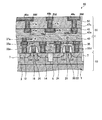
図1は、この発明の半導体装置の一例を概略的に示す断面図である。同図に示す半導体装置60は、半導体基板10と、半導体基板10に形成された回路素子20,30と、回路素子20,30を覆うようにして半導体基板10上に形成された多層配線部55とを備えている。
FIG. 1 is a cross-sectional view schematically showing an example of the semiconductor device of the present invention. A
上記の半導体基板10は、シリコンのような元素半導体からなる基板であってもよいし、ガリウムヒ素のような化合物半導体からなる基板であってもよい。さらには、SOI(Silicon On Insulator)基板であってもよい。半導体基板10の所定箇所には、該半導体基板10に形成しようとする回路素子の種類に応じた所定の素子領域(ウェル)と、所定形状の素子分離領域とが形成される。図示の半導体基板10は、P- 型シリコン基板1の所定箇所にN型ウェル3およびP型ウェル5を形成し、さらに、各素子領域3,5を平面視上区画するようにして素子分離領域7を形成したものである。
The
回路素子としてどのような素子を形成するかは、半導体装置60に求められる機能等に応じて適宜選定される。図1に示す回路素子20,30は、いずれも電界効果トランジスタ(以下、「電界効果トランジスタ20」、「電界効果トランジスタ30」という。)である。電界効果トランジスタ20は、N型ウェル3に形成されたソース領域12およびドレイン領域14と、半導体基板10上にゲート絶縁膜16を介して配置されたゲート電極18と、ゲート電極18における線幅方向両側に配置されたサイドウォールスペーサSW,SWとを有している。また、電界効果トランジスタ30は、P型ウェル5に形成されたソース領域22およびドレイン領域24と、半導体基板10上にゲート絶縁膜26を介して配置されたゲート電極28と、ゲート電極28における線幅方向両側に配置されたサイドウォールスペーサSW,SWとを有している。
Which element is formed as the circuit element is appropriately selected according to the function required of the
多層配線部55は、その全体が多層銅配線部となっている(以下、「多層銅配線部55」という。)。この多層銅配線部55は、複数の層間絶縁膜と、これら複数の層間絶縁膜の各々に複数本ずつ形成されたダマシン銅配線と、1本のダマシン銅配線に少なくとも1つ配置されて、該ダマシン銅配線を該ダマシン銅配線が形成されている層間絶縁膜よりも下層側の配線または回路素子に接続するコンタクトプラグと、1本のダマシン銅配線に1つずつ配置されて該ダマシン銅配線および該ダマシン銅配線に接続されたコンタクトプラグそれぞれの側面および下面を覆うバリアメタル層とを有している。
The entire
多層配線部(多層銅配線部)55を構成する各層間絶縁膜は所望の無機材料または有機材料からなり、個々の層間絶縁膜には、最も下の層間絶縁膜を除き、該層間絶縁膜に形成されたコンタクトプラグを介して接続される下層側のダマシン銅配線に比べて幅狭の第1種ダマシン銅配線および幅広の第2種ダマシン銅配線が形成されている。第1種ダマシン銅配線および第2種ダマシン銅配線それぞれの数は、層間絶縁膜毎に適宜選定されている。これらのダマシン銅配線およびコンタクトプラグは所定のパターンの下に接続されて、回路素子(電界効果トランジスタ20,電界効果トランジスタ30)の各々と共に集積回路を形成している。
Each interlayer insulating film constituting the multilayer wiring portion (multilayer copper wiring portion) 55 is made of a desired inorganic material or organic material, and the individual interlayer insulating films are except for the lowermost interlayer insulating film. A narrower first type damascene copper wiring and a wider second type damascene copper wiring are formed as compared with the lower-layer damascene copper wiring connected through the formed contact plug. The numbers of the first type damascene copper wiring and the second type damascene copper wiring are appropriately selected for each interlayer insulating film. These damascene copper wirings and contact plugs are connected under a predetermined pattern to form an integrated circuit together with each of the circuit elements (
図1においては、各層間絶縁膜に形成されているダマシン銅配線およびコンタクトプラグのうち、最も下の第1層間絶縁膜35に形成されている4つの第1層コンタクトプラグ32a〜32dと4つの第1層ダマシン銅配線33a〜33d、下から2番目の第2層間絶縁膜40に形成されている1つの第2層コンタクトプラグ37a、上から2番目の第(n−1)層間絶縁膜45に形成されている1つの第(n−1)層コンタクトプラグ42aと3つの第(n−1)層ダマシン銅配線43a〜43c、および、最も上の第n層間絶縁膜50に形成されている3つの第n層コンタクトプラグ47a〜47cと3つの第n層ダマシン銅配線48a〜48cが現れている。第n層ダマシン銅配線48bは第1種ダマシン銅配線であり、第n層ダマシン銅配線48cは第2種ダマシン銅配線である。なお、下から2番目の第2層間絶縁膜40に形成されている第2層ダマシン銅配線は、図1には現れていない。上記の「n」は4以上の整数を表すが、「n」を2または3として多層銅配線部を構成することも可能である。
In FIG. 1, among the damascene copper wirings and contact plugs formed in each interlayer insulating film, four first
各コンタクトプラグおよびダマシン銅配線はデュアルダマシン構造を有しており、同じ層間絶縁膜に形成されて互いに接続されているダマシン銅配線およびコンタクトプラグは、各々が1つの銅層での一領域からなっている。図1においては、デュアルダマシン構造を有するダマシン銅配線とコンタクトプラグとを区別し易くするために、便宜上、両者の間に境界線を描いてある。 Each contact plug and damascene copper wiring has a dual damascene structure, and each damascene copper wiring and contact plug formed on the same interlayer insulating film and connected to each other is composed of one region of one copper layer. ing. In FIG. 1, for the sake of convenience, a boundary line is drawn between the damascene copper wiring having a dual damascene structure and the contact plug.
個々のバリアメタル層BMは、例えばタンタル(Ta)、チタン(Ti)、タングステン(W)、ルテニウム(Ru)等の金属や、これらの金属の窒化物もしくは窒化硅化物により形成されて、あるいは上記の金属からなる層と上記の窒化物もしくは窒化硅化物からなる層との積層物により形成されて、対応するコンタクトプラグおよびダマシン銅配線それぞれの側面および下面を覆っている。ただし、ダマシン銅配線の下面のうちでコンタクトプラグ上に位置する領域には、バリアメタル層は形成されていない。なお、各層間絶縁膜上には例えばシリコン窒化物やシリコン炭窒化物等によって形成されたライナー膜が設けられているが、図1においてはその図示を省略している。 Each barrier metal layer BM is formed of, for example, a metal such as tantalum (Ta), titanium (Ti), tungsten (W), ruthenium (Ru), a nitride or nitride nitride of these metals, or the above-mentioned And a layer made of the above-mentioned nitride or nitride nitride, and covers the side and bottom surfaces of the corresponding contact plug and damascene copper wiring. However, the barrier metal layer is not formed in the region located on the contact plug in the lower surface of the damascene copper wiring. Note that a liner film formed of, for example, silicon nitride or silicon carbonitride is provided on each interlayer insulating film, but the illustration thereof is omitted in FIG.
このような構造を有する半導体装置60の最大の特徴は、第1種ダマシン銅配線の数が第2種ダマシン銅配線の数よりも多い層間絶縁膜に形成されているダマシン銅配線、コンタクトプラグ、およびバリアメタル層での水素含量の最大値が、第1種ダマシン銅配線の数が第2種ダマシン銅配線の数よりも少ない層間絶縁膜に形成されているダマシン銅配線、コンタクトプラグ、およびバリアメタル層での水素含量の最大値よりも小さいという点にある。半導体装置60は、上記の特徴を有していることから、装置全体でのSIV耐性を向上させることが容易な半導体装置である。以下、図2〜4を参照して、その理由を説明する。
The greatest feature of the
なお、この発明でいう「水素含量」とは、核反応解析法(NRA;Nuclear Reaction Analysis) により測定した水素含量を意味する。また、「層間絶縁膜に形成されているダマシン銅配線、コンタクトプラグ、およびバリアメタル層での水素含量の最大値」とは、ダマシン銅配線からその真下のコンタクトプラグ、およびバリアメタル層へとNRAにより順次水素含量を測定したときの最大値を意味する。 The “hydrogen content” in the present invention means a hydrogen content measured by a nuclear reaction analysis method (NRA). “The maximum value of the hydrogen content in the damascene copper wiring, the contact plug, and the barrier metal layer formed in the interlayer insulating film” means that the NRA extends from the damascene copper wiring to the contact plug and the barrier metal layer immediately below. Means the maximum value when the hydrogen content is measured sequentially.
図2は、多層銅配線部を模擬したサンプルに水素プラズマ処理を施したときにおける当該サンプル中での水素含量の解析結果を示すグラフである。上記のサンプルでは、熱酸化膜が形成されたシリコンウェハ上にタンタル窒化物層とタンタル層との積層物、第1の銅層、タンタル層、および第2の銅層がこの順番で積層されており、水素プラズマ処理は、第1の銅層上にタンタル層を積層するのに先だって該第1の銅層上に生じた自然酸化膜(銅酸化膜)を除去するために施されている。同図には、水素プラズマによる処理時間が0秒、30秒、または180秒のときの解析結果が示されている。 FIG. 2 is a graph showing an analysis result of the hydrogen content in the sample when the hydrogen plasma treatment is performed on the sample simulating the multilayer copper wiring part. In the above sample, a stack of a tantalum nitride layer and a tantalum layer, a first copper layer, a tantalum layer, and a second copper layer are stacked in this order on a silicon wafer on which a thermal oxide film is formed. The hydrogen plasma treatment is performed to remove a natural oxide film (copper oxide film) generated on the first copper layer before the tantalum layer is laminated on the first copper layer. This figure shows the analysis results when the treatment time with hydrogen plasma is 0 seconds, 30 seconds, or 180 seconds.
本件発明者等は、この解析により、水素プラズマ処理を施した第1の銅層、該第1の銅層の下のタンタル層およびタンタル窒化物層、ならびに当該第1の銅層上のタンタル層にも水素原子が取り込まれ、その含量は水素プラズマによる処理時間が長くなる程多くなる傾向があることを明らかにした。この解析結果に基づけば、実際の半導体装置においても、ダマシン銅配線に生じた自然酸化膜を水素プラズマ処理で除去したときには、水素プラズマ処理を施したダマシン銅配線には勿論、該ダマシン銅配線に対応するバリアメタル層および当該ダマシン銅配線の上に形成されるバリアメタル層にも水素原子が取り込まれるものと考えられる。なお、図2に示されているタンタル層(第1の銅層の上のタンタル層)での水素原子の取り込みは、第1の銅層に取り込まれていた水素原子が拡散したことによるものと思われる。また、第2の銅層においても水素原子の存在が確認されたが、これは、第2の銅層を形成してからNRAによる水素含量の測定を行うまでの間に大気中の水分が第2の銅層に吸収された結果であると考えられる。
Based on this analysis, the inventors have found that the first copper layer subjected to the hydrogen plasma treatment, the tantalum layer and the tantalum nitride layer under the first copper layer, and the tantalum layer on the first copper layer. It has been clarified that hydrogen atoms are also taken in, and the content tends to increase as the treatment time with hydrogen plasma increases. Based on this analysis result, even in an actual semiconductor device, when the natural oxide film generated in the damascene copper wiring is removed by the hydrogen plasma treatment, the damascene copper wiring subjected to the hydrogen plasma treatment is of course included in the damascene copper wiring. It is considered that hydrogen atoms are also taken into the corresponding barrier metal layer and the barrier metal layer formed on the damascene copper wiring. Note that the uptake of hydrogen atoms in the tantalum layer (the tantalum layer on the first copper layer) shown in FIG. 2 is due to the diffusion of the hydrogen atoms taken up in the first copper layer. Seem. In addition, the presence of hydrogen atoms was also confirmed in the second copper layer. This is because the moisture in the atmosphere does not increase until the hydrogen content is measured by NRA after the second copper layer is formed. This is considered to be a result of absorption by the
上述の解析結果に基づき、本件発明者等は、1つのコンタクトプラグによって接続される上側のダマシン銅配線の線幅の方が下側のダマシン銅配線の線幅よりも狭い配線パターン(以下、「第1パターン」という。)、および、1つのコンタクトプラグによって接続される上側のダマシン銅配線の線幅の方が下側のダマシン銅配線の線幅よりも広い配線パターン(以下、「第2パターン」という。)のそれぞれについて、水素プラズマ処理とSIV耐性との関連性の有無を調べた。 Based on the above analysis results, the present inventors have developed a wiring pattern in which the upper damascene copper wiring connected by one contact plug is narrower than the lower damascene copper wiring (hereinafter, “ And a wiring pattern in which the upper damascene copper wiring connected by one contact plug is wider than the lower damascene copper wiring (hereinafter referred to as “second pattern”). ”) Was examined for the presence of a relationship between hydrogen plasma treatment and SIV resistance.
図3は、第1パターンでの水素プラズマによる処理時間と3000時間後の累積故障率との関係を示すグラフである。同図に示すデータは、線幅0.42μmの上層ダマシン銅配線(上側のダマシン銅配線)と線幅10μmの下層ダマシン銅配線(下側のダマシン銅配線)とを直径0.14μmのコンタクトプラグで接続してシリコンウェハ上に第1パターンを形成するに際にして、下層ダマシン銅配線に施す水素プラズマ処理での処理時間を適宜変更して6つの試料を作製し、各試料についてビア抵抗増加による3000時間後の累積故障率を200℃の温度条件下で求めたものである。1つの試料には10000個規模で第1配線パターンが形成されている。上層ダマシン銅配線に対応するバリアメタル層としてはタンタル層が用いられ、下層ダマシン銅配線に対応するバリアメタル層としてはタンタル窒化物層とタンタル層とがこの順番で積層された積層物が用いられている。水素プラズマ処理は、100%水素ガスを用いて行った。 FIG. 3 is a graph showing the relationship between the treatment time with hydrogen plasma in the first pattern and the cumulative failure rate after 3000 hours. The data shown in the figure shows that the upper damascene copper wiring (upper damascene copper wiring) having a line width of 0.42 μm and the lower damascene copper wiring (lower damascene copper wiring) having a line width of 10 μm are contact plugs having a diameter of 0.14 μm. When the first pattern is formed on the silicon wafer by connecting with the above, six samples are prepared by appropriately changing the processing time in the hydrogen plasma processing applied to the lower damascene copper wiring, and the via resistance is increased for each sample. Is the cumulative failure rate after 3000 hours under the temperature condition of 200 ° C. A first wiring pattern is formed on a scale of 10,000 pieces in one sample. A tantalum layer is used as the barrier metal layer corresponding to the upper layer damascene copper wiring, and a laminate in which the tantalum nitride layer and the tantalum layer are stacked in this order is used as the barrier metal layer corresponding to the lower layer damascene copper wiring. ing. The hydrogen plasma treatment was performed using 100% hydrogen gas.
図3から明らかなように、上記の第1パターンでは水素プラズマ処理を施さないときの累積故障率が最も低く、水素プラズマによる処理時間が長くなる程、累積故障率が高くなる傾向がある。水素プラズマによる処理時間が0(ゼロ)秒のときの累積故障率が0%であることから、当該第1パターンでは、下層ダマシン銅配線に生じた自然酸化膜がその上のバリアメタル層(タンタル層)によって還元されたものと考えられる。 As apparent from FIG. 3, in the first pattern, the cumulative failure rate when hydrogen plasma treatment is not performed is the lowest, and the cumulative failure rate tends to increase as the treatment time with hydrogen plasma becomes longer. Since the cumulative failure rate when the treatment time by hydrogen plasma is 0 (zero) seconds is 0%, in the first pattern, the natural oxide film generated in the lower damascene copper wiring is formed on the barrier metal layer (tantalum). Is considered to have been reduced by the layer).
図4は、第2パターンでの水素プラズマによる処理時間と3000時間後の累積故障率との関係を示すグラフである。同図に示すデータは、線幅10μmの上層ダマシン銅配線と線幅0.42μmの下層ダマシン銅配線とを直径0.14μmのコンタクトプラグで接続してシリコンウェハ上に第2パターンを形成するに際にして、下層ダマシン銅配線に施す水素プラズマ処理での処理時間を適宜変更して6つの試料を作製し、各試料について累積故障率を求めたものである。このデータは、上層ダマシン銅配線および下層ダマシン銅配線それぞれの線幅を除き、図3に示したデータを求めたときと同じ条件の下に測定されている。 FIG. 4 is a graph showing the relationship between the treatment time with hydrogen plasma in the second pattern and the cumulative failure rate after 3000 hours. The data shown in the figure is for forming a second pattern on a silicon wafer by connecting an upper damascene copper wiring having a line width of 10 μm and a lower damascene copper wiring having a line width of 0.42 μm with a contact plug having a diameter of 0.14 μm. At that time, six samples were prepared by appropriately changing the processing time in the hydrogen plasma processing applied to the lower damascene copper wiring, and the cumulative failure rate was obtained for each sample. This data is measured under the same conditions as those obtained for the data shown in FIG. 3 except for the line widths of the upper layer damascene copper wiring and the lower layer damascene copper wiring.
図4から明らかなように、上記の第2パターンでは水素プラズマ処理を施さないときの累積故障率が最も高く、水素プラズマ処理を15秒以上施した各試料での累積故障率は、いずれの試料においても0%であった。したがって、当該第2パターンは下層ダマシン銅配線に生じた自然酸化膜の影響を強く受けるものの、水素含量の増加とSIV耐性との間には殆ど相関がないものと推察される。 As is clear from FIG. 4, in the second pattern, the cumulative failure rate when hydrogen plasma treatment is not performed is the highest, and the cumulative failure rate for each sample subjected to hydrogen plasma treatment for 15 seconds or more is any sample. It was also 0%. Therefore, although the second pattern is strongly influenced by the natural oxide film generated in the lower damascene copper wiring, it is presumed that there is almost no correlation between the increase in the hydrogen content and the SIV resistance.
このように、第1パターンと第2パターンとではSIV耐性に及ぼす水素含量の影響が互いに背反することが本件発明者等の研究によって明らかとなった。SIV耐性に優れた第1パターンを形成するうえからは、水素プラズマによる処理時間をできるだけ短くすることが望まれ、水素プラズマ処理を省略することさえも可能である。一方、SIV耐性に優れた第2パターンを形成するうえからは、水素プラズマ処理を施すことが実質的に必須である。 As described above, it has been clarified by the study by the present inventors that the influence of the hydrogen content on the SIV resistance is mutually contradictory between the first pattern and the second pattern. In order to form the first pattern excellent in SIV resistance, it is desired to shorten the treatment time by hydrogen plasma as much as possible, and it is possible to omit the hydrogen plasma treatment. On the other hand, in order to form the second pattern having excellent SIV resistance, it is substantially essential to perform a hydrogen plasma treatment.
実際の半導体装置では、通常、上記第1パターンでの上層ダマシン銅配線に相当するダマシン銅配線(この発明でいう「第1種ダマシン銅配線」)と上記第2パターンでの上層ダマシン銅配線に相当するダマシン銅配線(この発明でいう「第2種ダマシン銅配線」)とが1つの層間絶縁膜に混在し、これらのダマシン銅配線の個数比は層間絶縁膜毎に異なっている。このため、当該半導体装置全体でのSIV耐性を向上させるうえからは、多層配線部(多層銅配線部)を構成する個々の層間絶縁膜にバリアメタル層BMを形成するのに先だって行われる水素プラズマ処理での処理時間を一定にするのではなく、各層間絶縁膜での第1種ダマシン銅配線と第2種ダマシン銅配線との個数比に応じて水素プラズマによる処理時間を適宜調整することが望まれる。第1種ダマシン銅配線の個数比が高い層間絶縁膜については、第1種ダマシン銅配線の個数比が低い層間絶縁膜に比べて水素プラズマによる処理時間を短くすることが望まれる。 In an actual semiconductor device, usually, a damascene copper wiring corresponding to the upper layer damascene copper wiring in the first pattern (“first type damascene copper wiring” in the present invention) and an upper layer damascene copper wiring in the second pattern are used. Corresponding damascene copper wiring (“second type damascene copper wiring” in the present invention) is mixed in one interlayer insulating film, and the number ratio of these damascene copper wirings is different for each interlayer insulating film. For this reason, in order to improve the SIV resistance of the semiconductor device as a whole, hydrogen plasma is performed prior to forming the barrier metal layer BM in each interlayer insulating film constituting the multilayer wiring portion (multilayer copper wiring portion). Instead of making the processing time in the processing constant, the processing time by hydrogen plasma can be appropriately adjusted according to the number ratio of the first type damascene copper wiring and the second type damascene copper wiring in each interlayer insulating film. desired. For an interlayer insulating film having a high number ratio of the first type damascene copper wiring, it is desirable to shorten the processing time by hydrogen plasma compared to an interlayer insulating film having a low number ratio of the first type damascene copper wiring.
上述のようにして水素プラズマによる処理時間を調整すると、図1に示した半導体装置60におけるように、第1種ダマシン銅配線の数が第2種ダマシン銅配線の数よりも多い層間絶縁膜に形成されたダマシン銅配線、コンタクトプラグ、およびバリアメタル層での水素含量の最大値が、第1種ダマシン銅配線の数が第2種ダマシン銅配線の数よりも少ない層間絶縁膜に形成されたダマシン銅配線、コンタクトプラグ、およびバリアメタル層での水素含量の最大値よりも小さくなる。
When the processing time by hydrogen plasma is adjusted as described above, as in the
したがって半導体装置60は、装置全体でのSIV耐性を向上させることが容易な半導体装置である。個々の層間絶縁膜に形成されているダマシン銅配線、コンタクトプラグ、およびバリアメタル層での水素含量の最大値をどの程度にするか、換言すれば層間絶縁膜にバリアメタル層を形成するのに先だって行われる水素プラズマ処理での処理時間をどの程度にするかは、当該層間絶縁膜における第1種ダマシン銅配線と第2種ダマシン銅配線との個数比等に応じて適宜選定される。通常、上記の最大値は0.1×10²¹〜5.0×10²¹atoms/cc(0.1×1021〜5.0×1021atoms/cm3) の範囲内となる。
Therefore, the
実施の形態2.
上述した半導体装置60は、例えばこの発明の半導体装置の製造方法により得ることができる。当該製造方法は、層間絶縁膜積層工程と自然酸化膜除去工程とを含んでいる。自然酸化膜除去工程を行った後には、所定の後工程が行われる。以下、工程毎に詳述する。
The
(層間絶縁膜積層工程)
層間絶縁膜積層工程では、バリアメタル層、コンタクトプラグ、およびダマシン銅配線がそれぞれ複数形成された配線済み層間絶縁膜上に電気絶縁膜を形成した後にこの電気絶縁膜をパターニングして、ダマシン銅配線が形成される複数のトレンチと、コンタクトプラグが形成される複数のビアホールとを有する未配線層間絶縁膜を得る。この未配線層間絶縁膜に形成される複数のトレンチは、ビアホールの底に露出しているダマシン銅配線に比べて幅狭の第1種ダマシン銅配線が形成される第1種トレンチと、幅広の第2種ダマシン銅配線が形成される第2種トレンチとを含む。
(Interlayer insulation film lamination process)
In the interlayer insulating film laminating step, an electrical insulating film is formed on a wired interlayer insulating film on which a plurality of barrier metal layers, contact plugs, and damascene copper wirings are respectively formed, and then the electrical insulating film is patterned to form a damascene copper wiring. A non-wiring interlayer insulating film having a plurality of trenches in which the contact plugs are formed and a plurality of via holes in which contact plugs are formed is obtained. The plurality of trenches formed in the non-wiring interlayer insulating film include a first type trench in which a first type damascene copper wiring narrower than a damascene copper wiring exposed at the bottom of the via hole is formed, and a wide trench A second type trench in which a second type damascene copper wiring is formed.
上記の配線済み層間絶縁膜は、多層銅配線部を構成するいずれの層間絶縁膜(ただし、最も上の層間絶縁膜を除く。)であってもよい。多層銅配線部の下には所望の回路素子が形成された半導体基板が位置するわけであるが、これら半導体基板および回路素子の形成方法は特に限定されるものではなく、製造しようとする半導体装置の用途や該半導体装置に求められる機能あるいは性能等に応じて種々の方法により製造される。配線済み層間絶縁膜の形成、および該配線済み層間絶縁膜におけるバリアメタル層、コンタクトプラグ、およびダマシン銅配線の形成は、以下に説明する未配線層間絶縁膜の形成、および該未配線層間絶縁膜におけるバリアメタル層、コンタクトプラグ、およびダマシン銅配線の形成と同様にして行われるので、ここではその説明を省略する。 The wired interlayer insulating film may be any interlayer insulating film (however, excluding the uppermost interlayer insulating film) constituting the multilayer copper wiring portion. A semiconductor substrate on which desired circuit elements are formed is located under the multilayer copper wiring portion. However, the method for forming these semiconductor substrates and circuit elements is not particularly limited, and a semiconductor device to be manufactured. The semiconductor device is manufactured by various methods depending on the application and the function or performance required for the semiconductor device. The formation of the wired interlayer insulating film and the formation of the barrier metal layer, contact plug, and damascene copper wiring in the wired interlayer insulating film are performed as follows. Since this is performed in the same manner as the formation of the barrier metal layer, contact plug, and damascene copper wiring in FIG.
図5は、未配線層間絶縁膜の一例を概略的に示す断面図である。同図に示す未配線層間絶縁膜50は図1に示した第n層間絶縁膜50に相当するものであり、その下地となっている配線済み層間絶縁膜45は図1に示した第(n−1)層間絶縁膜45に相当するものであるので、図5に示した構成部材には図1で用いた参照符号と同じ参照符号を付してその説明を省略する。
FIG. 5 is a cross-sectional view schematically showing an example of an unwired interlayer insulating film. The non-wiring
同図に示す未配線層間絶縁膜50を得るにあたっては、例えば、所望の無機材料または有機材料によって電気絶縁膜を形成し、この電気絶縁膜上に所定形状のエッチングマスクを設けて当該電気絶縁膜を選択的にエッチングすることでダマシン銅配線形成用のトレンチを複数形成し、その後、上記のエッチングマスクに代えて他のエッチングマスクを設けて上記の電気絶縁膜を選択的にエッチングすることでコンタクトプラグ形成用のビアホールを複数形成する。これにより、配線済み層間絶縁膜45上に積層された未配線層間絶縁膜50が得られる。図5においては、未配線層間絶縁膜50に形成された複数のトレンチおよび複数のビアホールのうちの3つのトレンチT1 〜T3 と3つのビアホールV1 〜V3 とが現れている。上記3つのトレンチT1 〜T3 のち、トレンチT2 が第1種トレンチに相当し、トレンチT3 が第2種トレンチに相当する。
In obtaining the non-wiring
(自然酸化膜除去工程)
上述した未配線層間絶縁膜を配線済み層間絶縁膜上に積層すると、未配線層間絶縁膜に形成されたビアホールの底から露出しているダマシン銅配線の表面に不可避的に自然酸化膜(銅酸化膜)が生じるので、自然酸化膜除去工程では、水素ガスまたは水素原子を含有したガスを用いてこの自然酸化膜を除去する。
(Natural oxide film removal process)
When the above-mentioned non-wiring interlayer insulating film is laminated on the wired interlayer insulating film, a natural oxide film (copper oxide) is inevitably formed on the surface of the damascene copper wiring exposed from the bottom of the via hole formed in the non-wiring interlayer insulating film. Therefore, in the natural oxide film removing step, the natural oxide film is removed using hydrogen gas or a gas containing hydrogen atoms.
具体的には水素プラズマ処理や水素アニール処理、あるいは水素ラジカル処理によって上記の自然酸化膜を除去する。これらの方法で用いられる水素ガスに代えて、水素ガスと不活性ガス(ヘリウムガス、ネオンガス、アルゴンガス等)との混合ガス、または水素原子を含有した還元性ガス(アンモニアガス等)を用いたプラズマ処理、アニール処理、もしくはラジカル処理によって上記の自然酸化膜を除去することもできる。 Specifically, the natural oxide film is removed by hydrogen plasma treatment, hydrogen annealing treatment, or hydrogen radical treatment. Instead of the hydrogen gas used in these methods, a mixed gas of hydrogen gas and an inert gas (helium gas, neon gas, argon gas, etc.), or a reducing gas containing hydrogen atoms (ammonia gas, etc.) was used. The natural oxide film can also be removed by plasma treatment, annealing treatment, or radical treatment.
図6は、自然酸化膜除去工程の一例を概略的に断面図である。同図に示す例では、未配線層間絶縁膜50に形成された3つのビアホールV1 〜V3 それぞれの底から露出しているダマシン銅配線43a〜43cの表面に生じた自然酸化膜(銅酸化膜)COを、該自然酸化膜COに水素プラズマHPを照射することで除去している。
FIG. 6 is a schematic cross-sectional view of an example of the natural oxide film removing step. In the example shown in the drawing, a natural oxide film (copper oxide generated on the surface of the
このときの処理時間は、実施の形態1において既に説明したように、未配線層間絶縁膜45に形成されることになる第1種ダマシン銅配線と第2種ダマシン銅配線との個数比に応じて制御される。第1種ダマシン銅配線の個数比が1を超えるときには、第1種ダマシン銅配線の個数比が1未満であるときに比べて処理時間を短くすることが好ましい。なお、図示の例では、第1種トレンチであるトレンチT2 に形成されるダマシン銅配線が第1種ダマシン銅配線に相当し、第2種トレンチであるトレンチT3 に形成されるダマシン銅配線が第2種ダマシン銅配線に相当する。
The processing time at this time depends on the number ratio of the first type damascene copper wiring and the second type damascene copper wiring to be formed in the unwired
(後工程)
後工程では、上述のようにして自然酸化膜を除去した後の未配線層間絶縁膜50に、バリアメタル層、コンタクトプラグ、およびダマシン銅配線を形成する。バリアメタル層、コンタクトプラグ、およびダマシン銅配線の形成は、例えば次のようにして行われる。
(Post-process)
In the post-process, a barrier metal layer, a contact plug, and a damascene copper wiring are formed on the unwiring
まず、バリアメタル層の元となる無機膜をスパッタ法等の物理的気相蒸着法によって成膜し、その上にスパッタ法等の物理的気相蒸着法によって薄い銅層または薄い銅合金層を成膜する。無機膜上に形成する薄い銅層または薄い銅合金層は、ダマシン法によってコンタクトプラグおよびダマシン銅配線を形成するためのシードとして機能する。 First, an inorganic film serving as a base of the barrier metal layer is formed by physical vapor deposition such as sputtering, and a thin copper layer or thin copper alloy layer is formed thereon by physical vapor deposition such as sputtering. Form a film. A thin copper layer or a thin copper alloy layer formed on the inorganic film functions as a seed for forming a contact plug and a damascene copper wiring by a damascene method.
次に、上記のシードを電極として用いて電解めっきを行って、ビアホールおよびトレンチの各々を銅めっき層で埋める。この後、余剰の銅めっき層、すなわち未配線層間絶縁膜50の上面上に堆積した銅めっき層や各ビアホールおよび各トレンチに堆積した銅めっき層のうちで該ビアホールまたは該トレンチから溢れ出ている領域と、上記の無機膜のうちで未配線層間絶縁膜50の上面上に位置する領域とを化学的機械研磨(CMP)により除去する。
Next, electrolytic plating is performed using the above seed as an electrode, and each of the via hole and the trench is filled with a copper plating layer. Thereafter, the excess copper plating layer, that is, the copper plating layer deposited on the upper surface of the unwiring
図7は、バリアメタル層の元となる無機膜およびダマシン銅配線形成用のシードそれぞれの一例を概略的に示す断面図である。同図に示すように、バリアメタル層の元となる無機膜70は、各ビアホールV1 〜V3 の壁面、各ビアホールV1 〜V3 の底から露出しているダマシン銅配線43a〜43cの上面、各トレンチT1 〜T3 の壁面、および未配線層間絶縁膜50の上面を覆うようにして成膜される。また、シード72sは、無機膜70を覆うようにして該無機膜70上に成膜される。
FIG. 7 is a cross-sectional view schematically showing an example of each of an inorganic film serving as a base of a barrier metal layer and a seed for forming a damascene copper wiring. As shown in the figure, the
図8は、上述したシードを電極として用いた電解めっきにより形成される銅めっき層の一例を概略的に示す断面図である。同図に示す銅めっき層72は、シード72s(図7参照)とこのシード72s上に堆積した銅とからなり、各ビアホールV1 〜V3 および各トレンチT1 〜T3 を埋めていると共に、未配線層間絶縁膜50の上面を覆っている。
FIG. 8 is a cross-sectional view schematically showing an example of a copper plating layer formed by electrolytic plating using the above-described seed as an electrode.
図8に示した銅めっき層72および無機膜70の各々に対して上述のCMPを行うことにより、未配線層間絶縁膜50にバリアメタル層、コンタクトプラグ、およびダマシン銅配線がそれぞれ所定数形成される。図示の例では、図1に示した第n層コンタクトプラグ47a〜47c、および第n層ダマシン銅配線48a〜48cが未配線層間絶縁膜50に形成される。
By performing the above-described CMP on each of the
図1に示した半導体装置60は、同図に示した半導体基板10,回路素子(電界効果トランジスタ)20,30、第1層間絶縁膜35、第1層コンタクトプラグ32a〜32d、第1層ダマシン銅配線33a〜33d、ならびに各第1層コンタクトプラグおよび各第1層ダマシン銅配線に対応するバリアメタル層BMを所望の方法で形成した後、上述した層間絶縁膜積層工程、自然酸化膜除去工程、および後工程を必要回数繰り返して多層銅配線部(多層配線部)55を形成することで得られる。
A
以上、この発明の半導体装置およびその製造方法それぞれの実施の形態について説明したが、前述のように、この発明は上述した実施の形態に限定されるものではない。例えば、半導体装置を構成する多層配線部は、その全体を多層銅配線部とする他に、多層銅配線部と銅以外の導電性材料(例えばアルミニウム)により配線(ダマシン配線を含む。)が形成されている層間絶縁膜とを組み合わせて形成することもできる。アルミニウム配線が形成されている層間絶縁膜は、例えば多層銅配線部の上に配置される。 The embodiments of the semiconductor device and the manufacturing method thereof have been described above. However, as described above, the present invention is not limited to the above-described embodiments. For example, in the multilayer wiring part constituting the semiconductor device, in addition to the multilayer copper wiring part as a whole, wiring (including damascene wiring) is formed of the multilayer copper wiring part and a conductive material (for example, aluminum) other than copper. It can also be formed in combination with an interlayer insulating film. The interlayer insulating film in which the aluminum wiring is formed is disposed, for example, on the multilayer copper wiring portion.
アルミニウムを用いたデュアルダマシン配線は、例えば、バリアメタル層の元となる無機膜をビアホールの壁面、トレンチの壁面、および未配線層間絶縁膜の上面にそれぞれ成膜し、その上に低温環境下(例えば室温下)で薄いアルミニウム層をスパッタリング法により形成した後、高温環境下(アルミニウムがリフローを起こす温度環境下)でのスパッタリング法により上記薄いアルミニウム層上にアルミニウムを堆積させた後、余剰のアルミニウムおよび上記の無機膜のうちで層間絶縁膜の上面に位置している領域をCMPにより除去することで得られる。 In dual damascene wiring using aluminum, for example, an inorganic film as a base of a barrier metal layer is formed on the wall surface of a via hole, the wall surface of a trench, and the upper surface of a non-wiring interlayer insulating film, respectively, and a low temperature environment ( After forming a thin aluminum layer by sputtering, for example, at room temperature), after depositing aluminum on the thin aluminum layer by sputtering in a high temperature environment (a temperature environment in which aluminum reflows), surplus aluminum And it can be obtained by removing the region of the inorganic film located on the upper surface of the interlayer insulating film by CMP.
上述した実施の形態では各ダマシン銅配線がいずれもデュアルダマシン配線であるが、シングルダマシン配線であってもよい。その他、この発明の半導体装置およびその製造方法については種々の変形、修飾、組合せ等が可能である。 In the embodiment described above, each damascene copper wiring is a dual damascene wiring, but may be a single damascene wiring. In addition, the semiconductor device and the manufacturing method thereof according to the present invention can be variously modified, modified, combined, and the like.
10 半導体基板
20,30 回路素子(電界効果トランジスタ)
32a〜32d,37a,42a,47a〜47c コンタクトプラグ
33a〜33d,43a〜43c,48a ダマシン配線
45 第(n−1)層間絶縁膜(配線済み層間絶縁膜)
48b ダマシン配線(第1種ダマシン配線)
48c ダマシン銅配線(第2種ダマシン配線)
50 第n層間絶縁膜(配線層間絶縁膜)
55 多層配線部(多層銅配線部)
BM バリアメタル層
V1 〜V3 ビアホール
T1 トレンチ
T2 トレンチ(第1種トレンチ)
T3 トレンチ(第2種トレンチ)
10
32a to 32d, 37a, 42a, 47a to 47c Contact plugs 33a to 33d, 43a to 43c,
48b Damascene wiring (
48c Damascene copper wiring (
50 n-th interlayer insulating film (wiring interlayer insulating film)
55 Multilayer wiring part (Multilayer copper wiring part)
BM barrier metal layer V 1 to V 3 via hole T 1 trench T 2 trench (first type trench)
T 3 trench (
Claims (5)
前記多層銅配線部を構成する層間絶縁膜の各々には、前記多層銅配線部における最も下の層間絶縁膜を除き、該層間絶縁膜に形成されたコンタクトプラグを介して接続される下層側のダマシン銅配線に比べて幅狭の第1種ダマシン銅配線および幅広の第2種ダマシン銅配線が形成されており、
前記第1種ダマシン銅配線の数が前記第2種ダマシン銅配線の数よりも多い層間絶縁膜に形成されているダマシン銅配線、コンタクトプラグ、およびバリアメタル層での水素含量の最大値は、前記第1種ダマシン銅配線の数が前記第2種ダマシン銅配線の数よりも少ない層間絶縁膜に形成されているダマシン銅配線、コンタクトプラグ、およびバリアメタル層での水素含量の最大値よりも小さいことを特徴とする半導体装置。 A semiconductor substrate, a circuit element formed on the semiconductor substrate, and a multilayer copper wiring portion formed on the semiconductor substrate so as to cover the circuit element, the multilayer copper wiring portion including a plurality of interlayer insulations A film, a plurality of damascene copper wirings formed on each of the plurality of interlayer insulating films, and at least one damascene copper wiring are disposed on the damascene copper wiring. Contact plugs connected to wirings or circuit elements below the interlayer insulating film, and one each of the contact plugs arranged in one damascene copper wiring and connected to the damascene copper wiring and the damascene copper wiring. A semiconductor device having a barrier metal layer covering side and bottom surfaces,
In each of the interlayer insulating films constituting the multilayer copper wiring portion, except for the lowermost interlayer insulating film in the multilayer copper wiring portion, a lower layer side connected via a contact plug formed in the interlayer insulating film The first type damascene copper wiring and the second type damascene copper wiring which are narrower than the damascene copper wiring are formed.
The maximum value of the hydrogen content in the damascene copper wiring, the contact plug, and the barrier metal layer formed in the interlayer insulating film in which the number of the first type damascene copper wiring is larger than the number of the second type damascene copper wiring is: More than the maximum value of the hydrogen content in the damascene copper wiring, the contact plug, and the barrier metal layer formed in the interlayer insulating film in which the number of the first type damascene copper wiring is smaller than the number of the second type damascene copper wiring. A semiconductor device characterized by being small.
バリアメタル層、コンタクトプラグ、およびダマシン銅配線がそれぞれ複数形成された配線済み層間絶縁膜上に電気絶縁膜を形成した後に該電気絶縁膜をパターニングして、ダマシン銅配線が形成される複数のトレンチと、コンタクトプラグが形成される複数のビアホールとを有する未配線層間絶縁膜を得る層間絶縁膜積層工程と、
前記ビアホールの底に露出しているダマシン銅配線の表面に生じた自然酸化膜を、水素ガスまたは水素原子を含有したガスを用いて除去する自然酸化膜除去工程と、
を含み、
前記層間絶縁膜積層工程で前記未配線層間絶縁膜に形成される複数のトレンチは、前記ビアホールの底に露出しているダマシン銅配線に比べて幅狭の第1種ダマシン銅配線が形成される第1種トレンチおよび幅広の第2種ダマシン銅配線が形成される第2種トレンチを含み、
前記自然酸化膜除去工程で前記自然酸化膜を除去する際の処理時間は、前記未配線層間絶縁膜に形成されることになる前記第1種ダマシン銅配線と前記第2種ダマシン銅配線との個数比に応じて制御されることを特徴とする半導体装置の製造方法。 A semiconductor substrate, a circuit element formed on the semiconductor substrate, and a multilayer copper wiring portion formed on the semiconductor substrate so as to cover the circuit element, the multilayer copper wiring portion including a plurality of interlayer insulations A film, a plurality of damascene copper wirings formed on each of the plurality of interlayer insulating films, and at least one damascene copper wiring are disposed on the damascene copper wiring. Contact plugs connected to wirings or circuit elements below the interlayer insulating film, and one each of the contact plugs arranged in one damascene copper wiring and connected to the damascene copper wiring and the damascene copper wiring. A method of manufacturing a semiconductor device having a barrier metal layer covering side and bottom surfaces,
A plurality of trenches in which a damascene copper wiring is formed by forming an electrical insulating film on a wired interlayer insulating film in which a plurality of barrier metal layers, contact plugs, and damascene copper wirings are respectively formed, and then patterning the electrical insulating film And an interlayer insulating film laminating step for obtaining an unwired interlayer insulating film having a plurality of via holes in which contact plugs are formed,
A natural oxide film removing step of removing a natural oxide film formed on the surface of the damascene copper wiring exposed at the bottom of the via hole using a hydrogen gas or a gas containing hydrogen atoms;
Including
In the plurality of trenches formed in the non-wiring interlayer insulating film in the interlayer insulating film stacking step, the first type damascene copper wiring narrower than the damascene copper wiring exposed at the bottom of the via hole is formed. A second type trench in which a first type trench and a wide second type damascene copper wiring are formed,
The processing time for removing the natural oxide film in the natural oxide film removing step is the time between the first type damascene copper wiring and the second type damascene copper wiring to be formed in the unwired interlayer insulating film. A method of manufacturing a semiconductor device, wherein the method is controlled according to a number ratio.
Priority Applications (1)
| Application Number | Priority Date | Filing Date | Title |
|---|---|---|---|
| JP2006073419A JP2007250907A (en) | 2006-03-16 | 2006-03-16 | Semiconductor device and manufacturing method therefor |
Applications Claiming Priority (1)
| Application Number | Priority Date | Filing Date | Title |
|---|---|---|---|
| JP2006073419A JP2007250907A (en) | 2006-03-16 | 2006-03-16 | Semiconductor device and manufacturing method therefor |
Publications (1)
| Publication Number | Publication Date |
|---|---|
| JP2007250907A true JP2007250907A (en) | 2007-09-27 |
Family
ID=38594866
Family Applications (1)
| Application Number | Title | Priority Date | Filing Date |
|---|---|---|---|
| JP2006073419A Pending JP2007250907A (en) | 2006-03-16 | 2006-03-16 | Semiconductor device and manufacturing method therefor |
Country Status (1)
| Country | Link |
|---|---|
| JP (1) | JP2007250907A (en) |
Cited By (22)
| Publication number | Priority date | Publication date | Assignee | Title |
|---|---|---|---|---|
| WO2014013941A1 (en) * | 2012-07-18 | 2014-01-23 | 東京エレクトロン株式会社 | Method for manufacturing semiconductor device |
| US8853080B2 (en) | 2012-09-09 | 2014-10-07 | Novellus Systems, Inc. | Method for depositing tungsten film with low roughness and low resistivity |
| US9076843B2 (en) | 2001-05-22 | 2015-07-07 | Novellus Systems, Inc. | Method for producing ultra-thin tungsten layers with improved step coverage |
| US9153486B2 (en) | 2013-04-12 | 2015-10-06 | Lam Research Corporation | CVD based metal/semiconductor OHMIC contact for high volume manufacturing applications |
| US9159571B2 (en) | 2009-04-16 | 2015-10-13 | Lam Research Corporation | Tungsten deposition process using germanium-containing reducing agent |
| US9236297B2 (en) | 2009-04-16 | 2016-01-12 | Novellus Systems, Inc. | Low tempature tungsten film deposition for small critical dimension contacts and interconnects |
| US9240347B2 (en) | 2012-03-27 | 2016-01-19 | Novellus Systems, Inc. | Tungsten feature fill |
| US9589808B2 (en) | 2013-12-19 | 2017-03-07 | Lam Research Corporation | Method for depositing extremely low resistivity tungsten |
| US9613818B2 (en) | 2015-05-27 | 2017-04-04 | Lam Research Corporation | Deposition of low fluorine tungsten by sequential CVD process |
| US9754824B2 (en) | 2015-05-27 | 2017-09-05 | Lam Research Corporation | Tungsten films having low fluorine content |
| US9953984B2 (en) | 2015-02-11 | 2018-04-24 | Lam Research Corporation | Tungsten for wordline applications |
| US9978605B2 (en) | 2015-05-27 | 2018-05-22 | Lam Research Corporation | Method of forming low resistivity fluorine free tungsten film without nucleation |
| US10256142B2 (en) | 2009-08-04 | 2019-04-09 | Novellus Systems, Inc. | Tungsten feature fill with nucleation inhibition |
| CN111146147A (en) * | 2019-12-30 | 2020-05-12 | 中芯集成电路(宁波)有限公司 | A semiconductor device integration structure and method |
| CN113380709A (en) * | 2020-05-28 | 2021-09-10 | 台湾积体电路制造股份有限公司 | Semiconductor structure and forming method thereof |
| US11348795B2 (en) | 2017-08-14 | 2022-05-31 | Lam Research Corporation | Metal fill process for three-dimensional vertical NAND wordline |
| US11549175B2 (en) | 2018-05-03 | 2023-01-10 | Lam Research Corporation | Method of depositing tungsten and other metals in 3D NAND structures |
| US11972952B2 (en) | 2018-12-14 | 2024-04-30 | Lam Research Corporation | Atomic layer deposition on 3D NAND structures |
| US12002679B2 (en) | 2019-04-11 | 2024-06-04 | Lam Research Corporation | High step coverage tungsten deposition |
| US12077858B2 (en) | 2019-08-12 | 2024-09-03 | Lam Research Corporation | Tungsten deposition |
| US12237221B2 (en) | 2019-05-22 | 2025-02-25 | Lam Research Corporation | Nucleation-free tungsten deposition |
| US12444651B2 (en) | 2009-08-04 | 2025-10-14 | Novellus Systems, Inc. | Tungsten feature fill with nucleation inhibition |
-
2006
- 2006-03-16 JP JP2006073419A patent/JP2007250907A/en active Pending
Cited By (32)
| Publication number | Priority date | Publication date | Assignee | Title |
|---|---|---|---|---|
| US9076843B2 (en) | 2001-05-22 | 2015-07-07 | Novellus Systems, Inc. | Method for producing ultra-thin tungsten layers with improved step coverage |
| US9583385B2 (en) | 2001-05-22 | 2017-02-28 | Novellus Systems, Inc. | Method for producing ultra-thin tungsten layers with improved step coverage |
| US9236297B2 (en) | 2009-04-16 | 2016-01-12 | Novellus Systems, Inc. | Low tempature tungsten film deposition for small critical dimension contacts and interconnects |
| US9673146B2 (en) | 2009-04-16 | 2017-06-06 | Novellus Systems, Inc. | Low temperature tungsten film deposition for small critical dimension contacts and interconnects |
| US9159571B2 (en) | 2009-04-16 | 2015-10-13 | Lam Research Corporation | Tungsten deposition process using germanium-containing reducing agent |
| US10103058B2 (en) | 2009-08-04 | 2018-10-16 | Novellus Systems, Inc. | Tungsten feature fill |
| US12444651B2 (en) | 2009-08-04 | 2025-10-14 | Novellus Systems, Inc. | Tungsten feature fill with nucleation inhibition |
| US9653353B2 (en) | 2009-08-04 | 2017-05-16 | Novellus Systems, Inc. | Tungsten feature fill |
| US10256142B2 (en) | 2009-08-04 | 2019-04-09 | Novellus Systems, Inc. | Tungsten feature fill with nucleation inhibition |
| US9240347B2 (en) | 2012-03-27 | 2016-01-19 | Novellus Systems, Inc. | Tungsten feature fill |
| WO2014013941A1 (en) * | 2012-07-18 | 2014-01-23 | 東京エレクトロン株式会社 | Method for manufacturing semiconductor device |
| JPWO2014013941A1 (en) * | 2012-07-18 | 2016-06-30 | 東京エレクトロン株式会社 | Manufacturing method of semiconductor device |
| US8853080B2 (en) | 2012-09-09 | 2014-10-07 | Novellus Systems, Inc. | Method for depositing tungsten film with low roughness and low resistivity |
| US9153486B2 (en) | 2013-04-12 | 2015-10-06 | Lam Research Corporation | CVD based metal/semiconductor OHMIC contact for high volume manufacturing applications |
| US9589808B2 (en) | 2013-12-19 | 2017-03-07 | Lam Research Corporation | Method for depositing extremely low resistivity tungsten |
| US10529722B2 (en) | 2015-02-11 | 2020-01-07 | Lam Research Corporation | Tungsten for wordline applications |
| US9953984B2 (en) | 2015-02-11 | 2018-04-24 | Lam Research Corporation | Tungsten for wordline applications |
| US9754824B2 (en) | 2015-05-27 | 2017-09-05 | Lam Research Corporation | Tungsten films having low fluorine content |
| US10546751B2 (en) | 2015-05-27 | 2020-01-28 | Lam Research Corporation | Forming low resistivity fluorine free tungsten film without nucleation |
| US9613818B2 (en) | 2015-05-27 | 2017-04-04 | Lam Research Corporation | Deposition of low fluorine tungsten by sequential CVD process |
| US9978605B2 (en) | 2015-05-27 | 2018-05-22 | Lam Research Corporation | Method of forming low resistivity fluorine free tungsten film without nucleation |
| US11348795B2 (en) | 2017-08-14 | 2022-05-31 | Lam Research Corporation | Metal fill process for three-dimensional vertical NAND wordline |
| US11549175B2 (en) | 2018-05-03 | 2023-01-10 | Lam Research Corporation | Method of depositing tungsten and other metals in 3D NAND structures |
| US11972952B2 (en) | 2018-12-14 | 2024-04-30 | Lam Research Corporation | Atomic layer deposition on 3D NAND structures |
| US12002679B2 (en) | 2019-04-11 | 2024-06-04 | Lam Research Corporation | High step coverage tungsten deposition |
| US12237221B2 (en) | 2019-05-22 | 2025-02-25 | Lam Research Corporation | Nucleation-free tungsten deposition |
| US12077858B2 (en) | 2019-08-12 | 2024-09-03 | Lam Research Corporation | Tungsten deposition |
| CN111146147B (en) * | 2019-12-30 | 2023-04-28 | 中芯集成电路(宁波)有限公司 | A semiconductor device integration structure and method |
| CN111146147A (en) * | 2019-12-30 | 2020-05-12 | 中芯集成电路(宁波)有限公司 | A semiconductor device integration structure and method |
| CN113380709B (en) * | 2020-05-28 | 2024-10-18 | 台湾积体电路制造股份有限公司 | Semiconductor structure and forming method thereof |
| US12237229B2 (en) | 2020-05-28 | 2025-02-25 | Taiwan Semiconductor Manufacturing Co., Ltd. | Shallow trench isolation structures having uniform step heights |
| CN113380709A (en) * | 2020-05-28 | 2021-09-10 | 台湾积体电路制造股份有限公司 | Semiconductor structure and forming method thereof |
Similar Documents
| Publication | Publication Date | Title |
|---|---|---|
| US11488862B2 (en) | Semiconductor device with reduced via resistance | |
| JP2007250907A (en) | Semiconductor device and manufacturing method therefor | |
| KR101116785B1 (en) | Semiconductor device and method of manufacturing same | |
| TWI518843B (en) | Inner connection structure and method for forming interconnection structure | |
| TW200805563A (en) | Process for producing semiconductor integrated circuit device | |
| JP4917249B2 (en) | Semiconductor device and manufacturing method of semiconductor device | |
| US20120100689A1 (en) | Mim capacitor and associated production method | |
| JP2007109736A (en) | Semiconductor device and manufacturing method thereof | |
| CN112530860A (en) | Method for forming semiconductor device | |
| JP4878434B2 (en) | Semiconductor device and manufacturing method thereof | |
| KR100939773B1 (en) | Metal wiring of semiconductor device and forming method thereof | |
| KR100924556B1 (en) | Metal wiring of semiconductor device and method of forming the same | |
| JP2024000935A (en) | Semiconductor device and its manufacturing method | |
| JP2009170665A (en) | Semiconductor device and manufacturing method of semiconductor device | |
| JP2012009617A (en) | Semiconductor device manufacturing method, copper alloy for wiring, and semiconductor device | |
| KR20100036008A (en) | Method for forming metal wiring of semiconductor device | |
| JP2008147252A (en) | Semiconductor device and method for manufacturing the same | |
| KR100924557B1 (en) | Metal wiring of semiconductor device and method of forming the same | |
| KR100753132B1 (en) | Metal wiring formation method using dual damascene process | |
| KR20080114057A (en) | Wiring of a semiconductor device and its formation method | |
| JP2008103575A (en) | Semiconductor device and manufacturing method of semiconductor device | |
| KR20070055910A (en) | How to form via contact structures using dual damascene technology | |
| KR20070023164A (en) | MIM capacitor of semiconductor device and manufacturing method thereof | |
| KR20090055852A (en) | Metal wiring of semiconductor device and manufacturing method |