JP2007158882A - Voltage controlled oscillator - Google Patents
Voltage controlled oscillator Download PDFInfo
- Publication number
- JP2007158882A JP2007158882A JP2005352988A JP2005352988A JP2007158882A JP 2007158882 A JP2007158882 A JP 2007158882A JP 2005352988 A JP2005352988 A JP 2005352988A JP 2005352988 A JP2005352988 A JP 2005352988A JP 2007158882 A JP2007158882 A JP 2007158882A
- Authority
- JP
- Japan
- Prior art keywords
- voltage
- control signal
- load
- controlled oscillator
- capacitance
- Prior art date
- Legal status (The legal status is an assumption and is not a legal conclusion. Google has not performed a legal analysis and makes no representation as to the accuracy of the status listed.)
- Pending
Links
Images


Classifications
-
- H—ELECTRICITY
- H03—ELECTRONIC CIRCUITRY
- H03B—GENERATION OF OSCILLATIONS, DIRECTLY OR BY FREQUENCY-CHANGING, BY CIRCUITS EMPLOYING ACTIVE ELEMENTS WHICH OPERATE IN A NON-SWITCHING MANNER; GENERATION OF NOISE BY SUCH CIRCUITS
- H03B5/00—Generation of oscillations using amplifier with regenerative feedback from output to input
- H03B5/30—Generation of oscillations using amplifier with regenerative feedback from output to input with frequency-determining element being electromechanical resonator
- H03B5/32—Generation of oscillations using amplifier with regenerative feedback from output to input with frequency-determining element being electromechanical resonator being a piezoelectric resonator
- H03B5/36—Generation of oscillations using amplifier with regenerative feedback from output to input with frequency-determining element being electromechanical resonator being a piezoelectric resonator active element in amplifier being semiconductor device
- H03B5/366—Generation of oscillations using amplifier with regenerative feedback from output to input with frequency-determining element being electromechanical resonator being a piezoelectric resonator active element in amplifier being semiconductor device and comprising means for varying the frequency by a variable voltage or current
Landscapes
- Oscillators With Electromechanical Resonators (AREA)
Abstract
【課題】温度補償制御信号および外部電圧周波数制御信号とは独立してMOSトランジスタの閾値電圧を制御可能でかつ、周波数の可変範囲を低下させることなく直線性も確保し、小型化を図ることのできる電圧制御型発振器を提供する。
【解決手段】増幅器と、圧電振動子と、前記圧電振動子の両端子間に、負荷容量1と負荷容量2を設け、前記負荷容量1として設けられた容量は、入力電圧に対して容量値変化の小さい可変容量で構成され、前記負荷容量2として設けられた容量は、入力電圧に対して容量値変化の大きい可変容量で構成する。
前記負荷容量1および2の制御端子に高周波除去抵抗を介し、温度補償制御信号と外部電圧周波数制御信号を重畳した信号を入力する。これにより、温度補償制御回路や外部電圧周波数制御回路の出力バイアスを任意に決定できる。
【選択図】図2The threshold voltage of a MOS transistor can be controlled independently of a temperature compensation control signal and an external voltage frequency control signal, and linearity is ensured without lowering the variable range of the frequency, thereby achieving miniaturization. Provided is a voltage-controlled oscillator.
A load capacitor 1 and a load capacitor 2 are provided between an amplifier, a piezoelectric vibrator, and both terminals of the piezoelectric vibrator, and the capacitor provided as the load capacitor 1 has a capacitance value with respect to an input voltage. The capacitance provided as the load capacitance 2 is constituted by a variable capacitance having a large capacitance value change with respect to the input voltage.
A signal obtained by superimposing a temperature compensation control signal and an external voltage frequency control signal is input to the control terminals of the load capacitors 1 and 2 via a high frequency elimination resistor. Thereby, the output bias of the temperature compensation control circuit or the external voltage frequency control circuit can be arbitrarily determined.
[Selection] Figure 2
Description
本発明は、電圧制御型発振器にかかり、特に電圧制御による温度補償型水晶発振器として用いる電圧制御型発振器に関する。 The present invention relates to a voltage controlled oscillator, and more particularly to a voltage controlled oscillator used as a temperature compensated crystal oscillator by voltage control.
近年、携帯電話機等の移動体通信機器の急速な発展に伴い、これらの通信機器には、温度補償性能、小型化、使用周波数の高周波化など数々の機能追加が求められてきている。この為、このような通信機器において、通信周波数の基準として用いられている水晶発振器においても通信機器と同様に、温度補償性能、小型化、高周波化等の要求がある。 In recent years, with the rapid development of mobile communication devices such as mobile phones, these communication devices have been required to add a number of functions such as temperature compensation performance, downsizing, and higher frequency of use. For this reason, in such a communication device, there is a demand for a temperature compensation performance, miniaturization, high frequency and the like in the crystal oscillator used as a reference for the communication frequency as well as the communication device.
温度補償水晶発振器は、温度補償機能を具備し、温度変化による周波数の変化を小さくした水晶発振器であり、携帯電話等の基準周波数源として広く使用されている。そして電圧制御型発振器は、発振ループ内の負荷容量として電圧により容量値を変更することができる可変容量素子を設け、この可変容量素子の端子電圧を制御することにより、負荷容量値を変化させて周波数を制御することができるようにした発振器である。温度補償水晶発振器としては、電圧制御型発振器における可変容量の端子電圧を制御して水晶振動子(圧電振動子)の温度特性をキャンセルさせるようにしたものがある。 The temperature-compensated crystal oscillator is a crystal oscillator that has a temperature compensation function and reduces a change in frequency due to a temperature change, and is widely used as a reference frequency source for mobile phones and the like. The voltage-controlled oscillator is provided with a variable capacitance element that can change the capacitance value according to the voltage as a load capacitance in the oscillation loop, and by changing the terminal voltage of the variable capacitance element, the load capacitance value can be changed. This is an oscillator that can control the frequency. As a temperature compensated crystal oscillator, there is one in which the temperature characteristic of a crystal resonator (piezoelectric resonator) is canceled by controlling a terminal voltage of a variable capacitor in a voltage controlled oscillator.
近年、温度補償水晶発振器は低位相ノイズ化、起動時間短縮化、温度補償の高精度化などに加えて、小型化への取り組みが進められている。水晶発振器の小型化を実現するためには水晶振動子の小型化が必須である。しかし、一般的に水晶振動子を小型化することにより可変容量の変化に対する周波数の変化の割合が小さくなる傾向がある。 In recent years, efforts have been made to reduce the size of temperature compensated crystal oscillators in addition to lower phase noise, shorter start-up time, and higher accuracy of temperature compensation. In order to reduce the size of the crystal oscillator, it is essential to reduce the size of the crystal resonator. However, in general, by reducing the size of the crystal resonator, the ratio of the frequency change to the variable capacitance tends to decrease.
そこで、負荷容量として使用される可変容量の制御電圧に対する容量の変化量を大きくする必要がある。例えば、特許文献1、2に示されているように、ソース端子とドレイン端子をショートしたMOSトランジスタのソース−ドレイン端子とゲート端子の間に生じる静電容量を用いることで制御電圧の変化に対して容量値の変化を大きくとることができ、水晶発振器の周波数変化の感度向上を図っている(図16参照)。
Therefore, it is necessary to increase the amount of change in the capacity with respect to the control voltage of the variable capacity used as the load capacity. For example, as shown in
例えば、図19にこの電圧制御型発振器の一例を示すように、帰還抵抗6とインバータを備えた増幅器1と、圧電振動子4と、前記圧電振動子の両端子に、可変容量として第1および第2のMOSトランジスタ8を接続したものが提案されている。この可変容量においては、第1および第2のMOSトランジスタ8のソース−ドレイン端子が短絡され、このソース−ドレイン端子と、前記第1および第2のMOSトランジスタのゲート端子間に生じる静電容量を、ゲート端子に接続される電圧源9で制御している。
この電圧制御型発振器では、負荷容量として、MOSトランジスタのソース−ドレイン端子とゲート端子の間に生じる静電容量を発振回路の増幅器および水晶振動子(圧電振動子)に直接接続し、MOSトランジスタのゲート電圧を制御してソース−ドレイン端子とゲート端子の間に生じる静電容量を変化させることにより、周波数を制御する。この場合、MOSトランジスタのゲート電圧がソース−ドレイン端子電圧+閾値電圧となったときに、ゲート酸化膜直下にチャネルが形成され、ゲート端子とチャネルすなわちソース−ドレイン端子間の静電容量が増大する(この電圧を容量切り替わり電圧とする。)。 In this voltage controlled oscillator, the capacitance generated between the source and drain terminals and the gate terminal of the MOS transistor is directly connected to the amplifier of the oscillation circuit and the crystal resonator (piezoelectric resonator) as the load capacitance, and the MOS transistor The frequency is controlled by controlling the gate voltage to change the capacitance generated between the source-drain terminal and the gate terminal. In this case, when the gate voltage of the MOS transistor becomes the source-drain terminal voltage + the threshold voltage, a channel is formed immediately below the gate oxide film, and the capacitance between the gate terminal and the channel, that is, the source-drain terminal increases. (This voltage is used as a capacitance switching voltage.)
上述した従来の電圧制御型発振器の第1の課題として、容量切り替わり電圧付近にて容量値が切り替わる際の周波数変化が急峻となり、直線性の確保が難しいという問題があった。これは、圧電振動子の周波数―容量特性がイクスポーネンシャルカーブを描くことから、容量切り替わり電圧以下と容量切り替わり電圧以上となるときの容量値差が大きいと、容量変化に対する周波数の可変範囲は大きくなる為である。 As a first problem of the above-described conventional voltage controlled oscillator, there is a problem in that it is difficult to ensure linearity because the frequency change becomes sharp when the capacitance value is switched near the capacitance switching voltage. This is because the frequency-capacitance characteristics of the piezoelectric vibrator draw an exponential curve, so if the capacitance value difference is large when the capacitance switching voltage is less than or greater than the capacitance switching voltage, the variable range of the frequency with respect to the capacitance change is This is because it grows.
また、第2の課題として、ソース−ドレイン端子のDCバイアスが発振回路の増幅器側で決定されてしまうため、容量切り替わり電圧を任意の値に設定することができず、任意のゲート電圧を中心に周波数を制御することができないという問題があった。 As a second problem, since the DC bias of the source-drain terminal is determined on the amplifier side of the oscillation circuit, the capacitance switching voltage cannot be set to an arbitrary value, and an arbitrary gate voltage is used as a center. There was a problem that the frequency could not be controlled.
また、第3の課題として、通常のCMOSプロセスではMOSトランジスタの閾値電圧のばらつきや温度特性に依存して容量切り替わり電圧も変化するため、温度補償制御信号および外部電圧周波数制御信号そのものにMOSトランジスタの閾値電圧のバラツキや温度特性をキャンセルさせる特性をもたせる必要があった。 As a third problem, in the normal CMOS process, the capacitance switching voltage also changes depending on variations in the threshold voltage of the MOS transistor and temperature characteristics. It was necessary to provide a characteristic for canceling variations in threshold voltage and temperature characteristics.
さらにまた、第4の課題として、容量切り替わり電圧以下となるときの容量値が大きい為、周波数可変範囲が小さく周波数の起動時間も遅くなるという課題があった。 Furthermore, as a fourth problem, there is a problem that the frequency variable range is small and the frequency start-up time is delayed because the capacitance value when the capacitance is equal to or lower than the capacitance switching voltage is large.
この為、実際にMOSトランジスタのソース−ドレイン端子とゲート端子の間に生じる静電容量を用いた水晶発振器の設計を容易にして実用化するためには、MOSトランジスタの端子間に生じる静電容量を拡大させ、容量値が緩やかに変化させるか、もしくはアレイ構造を用いることにより静電容量を拡大させ、かつMOSトランジスタの閾値電圧制御信号を温度補償制御信号および外部電圧周波数制御信号とは独立して制御する必要があるという問題があった。 For this reason, in order to easily and practically design a crystal oscillator using the capacitance generated between the source-drain terminal and the gate terminal of the MOS transistor, the capacitance generated between the terminals of the MOS transistor. The capacitance value is gradually changed or the capacitance is increased by using an array structure, and the threshold voltage control signal of the MOS transistor is made independent of the temperature compensation control signal and the external voltage frequency control signal. There was a problem that it was necessary to control.
本発明は前記実情に鑑みてなされたもので、電圧制御型発振器において、周波数の可変範囲を低下させることなく直線性も確保し、小型化を図ることのできる電圧制御型発振器を提供することを目的とする。 The present invention has been made in view of the above circumstances, and in a voltage controlled oscillator, provides a voltage controlled oscillator capable of ensuring linearity without reducing the variable range of frequency and reducing the size. Objective.
すなわち、MOSトランジスタの端子間に生じる静電容量の容量切り替わり電圧以下での容量値が大きくなるのを防ぐことにより特性改善を図り、外部入力電圧による周波数変化率が一定でかつ広範囲に可変させ、MOSトランジスタの閾値電圧をも同時に制御可能な電圧制御型発振器を提供することを目的とする。 In other words, the characteristics are improved by preventing the capacitance value below the capacitance switching voltage of the capacitance generated between the terminals of the MOS transistor from increasing, the frequency change rate due to the external input voltage is constant and variable over a wide range, An object of the present invention is to provide a voltage controlled oscillator capable of simultaneously controlling the threshold voltage of a MOS transistor.
上記目的を達成するため、本発明に係る電圧制御型発振器は、バイポーラトランジスタもしくはCMOSトランジスタと帰還抵抗とを備えた増幅器と、圧電振動子と、負荷容量として前記圧電振動子の両端子間に前記負荷容量1と前記負荷容量2とを備え、前記負荷容量1手段には入力電圧に対する容量変化の少ない可変容量を使用し、前記負荷容量2手段には入力電圧に対する容量変化の大きい可変容量を使用する構成を特徴としている。
In order to achieve the above object, a voltage-controlled oscillator according to the present invention includes an amplifier having a bipolar transistor or a CMOS transistor and a feedback resistor, a piezoelectric vibrator, and a load capacitor between both terminals of the piezoelectric vibrator. A load capacitor 1 and the
この構成によれば、入力電圧に対する負荷容量変化量の違う前記負荷容量1と2を合成することにより容量切り替わり電圧以下での周波数の可変範囲も確保し、容量切り替わり電圧以上でも周波数の可変範囲が確保可能となる。したがって入力電圧に対して周波数可変範囲の拡大ができる(図16参照)。
According to this configuration, by combining the
また、本発明に係る電圧制御型発振器は、前記負荷容量1手段として第1および第2のDCカット容量とからなる可変容量手段が、第1のMOSトランジスタで構成し、前記負荷容量2手段として設けられた可変容量は、第2と第3のMOSトランジスタで構成されている。前記負荷容量1手段の前記第1のMOSトランジスタのソース−ドレイン端子が短絡されこのソース−ドレイン端子と、前記第1のMOSトランジスタのゲート端子間に生じる静電容量で構成され、前記負荷容量2手段の前記第2のMOSトランジスタのソース−ドレイン端子は、前記圧電振動子と接続されている。また前記圧電振動子の他端と前記負荷容量2手段の第3のMOSトランジスタのソース−ドレイン端子が接続され、前記第2と第3のMOSトランジスタのゲートは共通接続される構成を特徴としている。
Further, in the voltage controlled oscillator according to the present invention, the variable capacitor means including the first and second DC cut capacitors as the load capacitor 1 means is constituted by a first MOS transistor, and the
この構成によれば、前記負荷容量1と2手段を構成しているMOSトランジスタの切り替わり電圧が第1と第2と第3のMOSトランジスタでそれぞれ変わることにより周波数可変幅の増大とともに直線性の改善を可能とすることができる。また、前記負荷容量1手段の第1のMOSトランジスタのゲートとソース−ドレイン端子の位相はおよそ180°ずれているため、ミラー効果によりMOS可変容量(バラクタ)の容量はおよそ2倍の容量値と等価となり、周波数を可変するのに必要な容量値に比べ小型化を図ることができる。また、MOSバラクタの制御電圧の変化に対する周波数の変化の割合、いわゆる周波数可変感度を大きく取ることができる。
According to this configuration, the switching voltage of the MOS transistors constituting the
また、本発明の電圧制御型発振器は、前記負荷容量1手段の前記第1のMOSトランジスタのソース−ドレイン端子と前記ゲート端子に逆の位相の発振電圧が印加され、前記負荷容量1手段の前記第1のMOSトランジスタのゲート端子に入力される前記第1の制御信号と、前記負荷容量2の前記第2および第3のMOSトランジスタのゲート端子に入力される第2の制御信号とにより発振周波数を制御するようにしたことを特徴とする。
In the voltage-controlled oscillator according to the present invention, an oscillation voltage having an opposite phase is applied to the source-drain terminal and the gate terminal of the first MOS transistor of the load capacitor 1 means, and the load capacitor 1 means The oscillation frequency is determined by the first control signal input to the gate terminal of the first MOS transistor and the second control signal input to the gate terminals of the second and third MOS transistors of the
この構成によれば、容量切り替わり電圧が前記負荷容量1と2手段を構成しているMOSトランジスタの切り替わり電圧がそれぞれ変わることにより周波数可変幅の増大とともに直線性の改善が可能とすることができる。また、独立して制御可能な第1および第2の制御信号を用いることにより、MOSトランジスタ閾値電圧を制御して容量切り替わり電圧を制御でき、任意の制御電圧値を中心に周波数を変化させることができる。またこの第1のMOSトランジスタのゲートとソース−ドレイン端子の位相はおよそ180°ずれているため、ミラー効果によりMOS可変容量(バラクタ)の容量はおよそ2倍の容量値と等価となる。したがって、MOSバラクタの制御電圧の変化に対する周波数の変化の割合、いわゆる周波数可変感度を大きく取ることができ、かつ同程度の周波数を可変するのに必要な容量値に比べ小型化を図ることができる。また、制御電圧のダイナミックレンジが広がるため、周波数変化幅を大きく取ることが可能となる。これにより、第2および第3のMOSトランジスタのサイズを小さくすることが可能となり、チップサイズの小型化が可能となる。
According to this configuration, it is possible to improve the linearity as the frequency variable width increases by changing the switching voltage of the MOS transistors constituting the
また、本発明の電圧制御型発振器は、前記負荷容量1と2の手段を各々複数具備し、各負荷容量に対して、各々独立した制御信号を入力することにより発振周波数を制御するようにしたものを含む。
The voltage-controlled oscillator according to the present invention includes a plurality of means for the
この構成によれば、容量の可変幅を広げることができる。 According to this configuration, the variable width of the capacity can be expanded.
また、本発明の電圧型発振器は、前記負荷容量1および2手段にて使用している前記第1と第2と第3のMOSトランジスタのバックゲート端子に高抵抗を接続した温度補償制御信号と外部電圧周波数制御信号およびMOSトランジスタ閾値電圧制御信号のいずれかの信号入力を行うことの可能な構成を含む。
The voltage type oscillator according to the present invention includes a temperature compensation control signal in which a high resistance is connected to back gate terminals of the first, second and third MOS transistors used in the
この構成によれば、バックゲートから高抵抗に接続されることによりドレイン−バックゲート間の容量切り替え電圧以下での容量値が小さくすることが可能となり、周波数可変幅および負性抵抗の増大を図ることができる。また、圧電振動子からみた容量値のバラツキを押さえることができる。 According to this configuration, by connecting the back gate to the high resistance, the capacitance value below the capacitance switching voltage between the drain and the back gate can be reduced, and the frequency variable width and the negative resistance are increased. be able to. In addition, it is possible to suppress variations in capacitance values viewed from the piezoelectric vibrator.
また、本発明の電圧制御型発振器は、前記第1および前記第2の制御信号が、温度補償制御信号と外部電圧周波数制御信号とを重畳した信号であり、前記第3の制御信号は、MOSトランジスタ閾値電圧制御信号であるものを含む。 In the voltage-controlled oscillator according to the present invention, the first and second control signals are signals in which a temperature compensation control signal and an external voltage frequency control signal are superimposed, and the third control signal is a MOS Includes what is a transistor threshold voltage control signal.
この構成によれば、圧電振動子の温度補償および、外部電圧周波数のばらつきを抑制することができる。 According to this configuration, temperature compensation of the piezoelectric vibrator and variation in external voltage frequency can be suppressed.
また、本発明の電圧制御型発振器は、前記第1および前記第2の制御信号は、MOSトランジスタ閾値電圧制御信号であり、前記第3の制御信号は、温度補償制御信号と外部電圧周波数制御信号とを重畳した信号であるものを含む。 In the voltage controlled oscillator of the present invention, the first and second control signals are MOS transistor threshold voltage control signals, and the third control signal is a temperature compensation control signal and an external voltage frequency control signal. And the signal that is superimposed.
この構成によれば、温度補償および、外部電圧周波数のばらつきを抑制することができる。 According to this configuration, temperature compensation and variations in external voltage frequency can be suppressed.
また、本発明の電圧制御型発振器は、前記第1または第2の制御信号の入力される端子が、温度特性ばらつきの解除機能を有する回路を具備したものを含む。 The voltage controlled oscillator according to the present invention includes one in which a terminal to which the first or second control signal is input includes a circuit having a function of canceling variation in temperature characteristics.
この構成によれば、MOSトランジスタの温度特性ばらつきをキャンセルし、高歩留化を図ることができる。 According to this configuration, it is possible to cancel the temperature characteristic variation of the MOS transistor and achieve a high yield.
また、本発明の電圧制御型発振器は、前記第1または第2また第3の制御信号の入力される端子が、低周波除去用のフィルター機能を有する回路を具備したものを含む。 The voltage controlled oscillator according to the present invention includes one in which the terminal to which the first, second or third control signal is input has a circuit having a filter function for removing low frequency.
この構成によれば、入力電圧から入力される電圧ノイズ成分が除去することが可能となり低ノイズ化が実現できる。 According to this configuration, it is possible to remove the voltage noise component input from the input voltage, thereby realizing low noise.
また、本発明の電圧制御型発振器は、前記第1または第2の制御信号の入力される端子が、調整電圧を格納した不揮発性記憶媒体を有する調整回路を具備したものを含む。 The voltage controlled oscillator according to the present invention includes a circuit in which a terminal to which the first or second control signal is input includes an adjustment circuit having a nonvolatile storage medium storing an adjustment voltage.
この構成によれば、あらかじめ決定しておいた調整用閾値電圧を不揮発性記憶媒体に保存しておき、この不揮発性記憶媒体から読み出して調整するようにすれば短時間で高精度の調整が可能となる。 According to this configuration, it is possible to perform high-precision adjustment in a short time by storing the adjustment threshold voltage determined in advance in the nonvolatile storage medium, and reading and adjusting from the nonvolatile storage medium. It becomes.
また、本発明の電圧制御型発振回路を含めた回路を圧電振動子と共にモジュール化を行ったものを含む。 Further, the circuit including the voltage controlled oscillation circuit of the present invention is modularized together with the piezoelectric vibrator.
このように、前記圧電振動子の前記負荷容量と周波数の特性より容量切り替わり電圧以下での容量値の最小化と周波数可変量の増大ができ、温度補償制御信号および外部電圧周波数制御信号とは独立してMOSトランジスタ閾値電圧を制御して容量切り替わり電圧を制御でき、任意の制御電圧値を中心に周波数を変化させることができる。 As described above, the capacitance value can be minimized and the frequency variable amount can be increased below the capacitance switching voltage from the load capacitance and frequency characteristics of the piezoelectric vibrator, independent of the temperature compensation control signal and the external voltage frequency control signal. Then, the MOS transistor threshold voltage can be controlled to control the capacitance switching voltage, and the frequency can be changed around an arbitrary control voltage value.
本発明によれば、容量切り替わり電圧以下での容量値の最小化を図ることで周波数拡大が可能となる。また温度補償制御信号および外部電圧周波数制御信号とは独立してMOSトランジスタ閾値電圧を制御することで容量切り替わり電圧を制御することができ、任意の制御電圧値を中心に周波数を変化させることができる。 According to the present invention, it is possible to expand the frequency by minimizing the capacitance value below the capacitance switching voltage. Further, the capacitance switching voltage can be controlled by controlling the MOS transistor threshold voltage independently of the temperature compensation control signal and the external voltage frequency control signal, and the frequency can be changed around any control voltage value. .
また、MOSトランジスタの閾値電圧ばらつきや温度特性をキャンセルさせる信号を、温度補償制御信号および外部電圧周波数制御信号とは独立して入力することができ、温度補償制御回路や外部電圧周波数制御回路の設計を容易にすることができる。 Also, a signal for canceling threshold voltage variations and temperature characteristics of MOS transistors can be input independently of the temperature compensation control signal and the external voltage frequency control signal, and the design of the temperature compensation control circuit and the external voltage frequency control circuit can be performed. Can be made easier.
このように、MOSトランジスタの端子間の静電容量を用いた電圧制御型発振器の実用化を図ることができるという効果を奏する。 Thus, there is an effect that the voltage controlled oscillator using the capacitance between the terminals of the MOS transistor can be put into practical use.
以下、図面を参照して本発明における実施の形態を詳細に説明する。 Hereinafter, embodiments of the present invention will be described in detail with reference to the drawings.
(実施の形態1)
図1は本発明の実施の形態1における電圧制御型発振器の概略構成を示す回路図である。
(Embodiment 1)
FIG. 1 is a circuit diagram showing a schematic configuration of the voltage controlled oscillator according to the first embodiment of the present invention.
本実施の形態1の電圧発振器では、図1に示すように前記負荷容量1として可変量の少ない可変容量1と可変容量2として可変量の大きい負荷容量2として構成している。
In the voltage oscillator according to the first embodiment, as shown in FIG. 1, the load capacitor 1 is configured as a variable capacitor 1 having a small variable amount and a
図17は、前記可変容量1と可変容量2にて構成された容量の入力電圧による変化特性を示す。
FIG. 17 shows a change characteristic of the capacitor constituted by the variable capacitor 1 and the
この図17より可変容量1の入力される電圧に対して緩やかに変化する容量値と可変容量2の入力される電圧に対して急峻に変化する容量値との合成容量が、容量と周波数の変化に対して一定の変化を行うことが可能となる。
As shown in FIG. 17, the combined capacitance of the capacitance value that gradually changes with respect to the voltage input to the variable capacitor 1 and the capacitance value that changes sharply with respect to the voltage that is input to the
これにより、温度補償制御回路や外部電圧周波数制御回路の設計を容易にすることが可能となり、さらに温度補償制御回路や外部電圧周波数制御回路の出力バイアスの出力Dレンジの拡大できることにより設計を容易に行うことが可能となる。 This makes it easy to design the temperature compensation control circuit and the external voltage frequency control circuit, and further facilitates the design by expanding the output D range of the output bias of the temperature compensation control circuit and the external voltage frequency control circuit. Can be done.
(実施の形態2)
図2は本発明の実施の形態2における電圧制御型発振器の概略構成を示す回路図である。
(Embodiment 2)
FIG. 2 is a circuit diagram showing a schematic configuration of the voltage controlled oscillator according to the second embodiment of the present invention.
本実施の形態2の電圧制御型発振器では、図2に示すように負荷容量として、例えば前記負荷容量1の第1のMOSトランジスタ13と前記負荷容量2のMOSトランジスタ14と15のソース端子とドレイン端子は、それぞれが短絡している。また、前記負荷容量1の第1のMOSトランジスタ13のゲート端子と前記負荷容量2の第2と第3のMOSトランジスタ14と15のゲート端子は、共通接続され、ゲート端子と第1と第2と第3のMOSトランジスタのソース−ドレイン端子間で構成された静電容量を使用した可変容量素子としている。
In the voltage controlled oscillator according to the second embodiment, as shown in FIG. 2, as load capacitors, for example, the
また、図3は本発明の実施の形態2におけるMOSトランジスタの別の使用例を示す図である。 FIG. 3 is a diagram showing another example of use of the MOS transistor according to the second embodiment of the present invention.
この本実施の形態2での前記負荷容量1と前記負荷容量2のMOSトランジスタの使用例は、例えば前記負荷容量1で使用している負荷容量について説明すると、第1のMOSトランジスタ13のソース端子とバックゲート端子を短絡している。前記負荷容量2の第2と第3のMOSトランジスタ14、15のソース端子とバックゲート端子を短絡している。前記負荷容量1の第1のMOSトランジスタ13のゲート端子と前記負荷容量2の第2、第3のMOSトランジスタ14と15のゲート端子は、共通接続され、ゲート端子と第1と第2と第3のMOSトランジスタのドレイン端子間で構成された静電容量を使用した可変容量素子で構成するものもある。
The usage example of the load capacitance 1 and the MOS transistor of the
また、図4は本発明の実施の形態2におけるMOSトランジスタの別の使用例を示す図である。 FIG. 4 is a diagram showing another example of use of the MOS transistor according to the second embodiment of the present invention.
この本実施の形態2での前記負荷容量1と前記負荷容量2のMOSトランジスタの使用例は、例えば前記負荷容量1で使用している負荷容量について説明すると、第1のMOSトランジスタ13のソース端子とドレイン端子を短絡し、かつ第4のMOSトランジスタ16のドレイン端子とも短絡接続し、第1と第4のMOSトランジスタ13,16のバックゲート端子は、第4のMOSトランジスタ16のソース端子と短絡接続している。また、第1と第2のMOSトランジスタ13,16のゲート端子は短絡し、前記第1のMOSトランジスタ13のソース、ドレイン端子と前記第2のトランジスタ16のドレイン端子と前記第1と前記第2のMOSトランジスタのゲート端子間で静電容量を使用した可変容量素子で構成するものもある。
The usage example of the load capacitance 1 and the MOS transistor of the
すなわちこの電圧制御型発振器は、図2に示すように、帰還回路を構成する帰還抵抗1と増幅器2とからなる発振増幅器と、水晶振動子3と、負荷容量とによって構成された電圧制御型発振回路を示しており、負荷容量として、前述したMOSトランジスタのドレイン−ゲート端子、ドレイン−バックゲート間に生じる静電容量を用いた可変容量として構成している。
That is, as shown in FIG. 2, this voltage controlled oscillator has a voltage controlled oscillation composed of an oscillation amplifier including a feedback resistor 1 and an
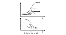
図16は、前記MOSトランジスタの端子間に生じる静電容量のC−V特性,f−V特性を示している。従来の特性MOSトランジスタの端子間を使用した特性を破線で示す。 FIG. 16 shows CV characteristics and fV characteristics of capacitance generated between the terminals of the MOS transistor. A characteristic using the terminals of the conventional characteristic MOS transistor is indicated by a broken line.
この図16より、容量Cは、一方の端子に印加される電圧に閾値電圧を加えた電圧で急峻に変化する。電圧Vは、他方の端子に印加されるMOSトランジスタ閾値電圧制御信号により任意に選ぶことができるため、容量切り替わり電圧すなわち周波数が切り替わる電圧を任意に選ぶことができる。これにより、温度補償制御回路や外部電圧周波数制御回路の出力バイアスを任意に決定することができ、設計を容易にすることができる。 From FIG. 16, the capacitance C changes sharply with a voltage obtained by adding a threshold voltage to the voltage applied to one terminal. Since the voltage V can be arbitrarily selected by the MOS transistor threshold voltage control signal applied to the other terminal, the capacitance switching voltage, that is, the voltage at which the frequency is switched can be arbitrarily selected. Thereby, the output bias of the temperature compensation control circuit or the external voltage frequency control circuit can be arbitrarily determined, and the design can be facilitated.
また、MOSトランジスタの閾値電圧制御信号としてばらつきや温度特性と逆の特性をもつ電圧を印加することにより、温度特性をキャンセルすることができ、温度補償信号や外部電圧周波数制御信号とは独立に容量切り替わり電圧のばらつきや温度特性をキャンセルすることが可能となり、さらに温度補償制御回路や外部電圧周波数制御回路の設計を容易にすることが可能となる。 In addition, by applying a voltage having a characteristic opposite to the variation or temperature characteristic as the threshold voltage control signal of the MOS transistor, the temperature characteristic can be canceled, and the capacitance is independent of the temperature compensation signal and the external voltage frequency control signal. Variations in switching voltage and temperature characteristics can be canceled, and furthermore, the design of a temperature compensation control circuit and an external voltage frequency control circuit can be facilitated.
また、前記本実施の形態2の前記負荷容量1では、MOSトランジスタのゲートとソース−ドレイン端子の位相は180°ずれている。このとき、ミラー効果によりMOS可変容量(バラクタ)の容量はおよそ2倍の容量値と等価となるため、MOSバラクタの制御電圧の変化に対する周波数の変化の割合、いわゆる周波数可変感度を大きく取ることができる。また、制御電圧のダイナミックレンジが広がるため、周波数変化幅を大きく取ることが可能となる。これにより、第1および第4のMOSトランジスタ13、16のサイズを小さくすることが可能となり、チップサイズの小型化にも貢献する。
In the load capacitor 1 of the second embodiment, the phases of the gate and source-drain terminals of the MOS transistor are shifted by 180 °. At this time, since the capacitance of the MOS variable capacitor (varactor) is equivalent to approximately twice the capacitance value due to the Miller effect, the ratio of the change in frequency to the change in the control voltage of the MOS varactor, so-called frequency variable sensitivity, can be increased. it can. In addition, since the dynamic range of the control voltage is expanded, it is possible to increase the frequency change width. As a result, the first and
(実施の形態3)
図5は本発明の実施の形態3における電圧制御型発振器の概略構成を示す回路図である。
(Embodiment 3)
FIG. 5 is a circuit diagram showing a schematic configuration of the voltage controlled oscillator according to the third embodiment of the present invention.
本実施の形態3は、図5に示すように前記実施の形態2の前記負荷容量1を複数接続した構成としている。部位については、実施の形態2と同様であり、説明は省略する他、同一部位については同一符号を付した。
In the third embodiment, as shown in FIG. 5, a plurality of the load capacitors 1 of the second embodiment are connected. About the site | part, it is the same as that of
この構成によれば、前記実施の形態2の電圧制御型発振器より周波数可変範囲は減少するが、前記負荷容量1として使用するMOSサイズ面積も少なくて済み、またMOSトランジスタのゲート端子、ソース−ドレイン端子には高周波除去抵抗21,22,23を介して、MOSトランジスタ閾値電圧制御信号または温度補償制御信号と外部電圧周波数制御信号のいずれかの信号が入力されるようにすることにより、素子単体の保有している温度特性のばらつきが低減されるとともに、外部周波数制御を行うことが可能となる。前記負荷容量1の構成を複数接続し、それぞれ個別に制御信号が与えられるように構成することで幅広い周波数可変範囲が実現可能となる。
According to this configuration, the frequency variable range is reduced as compared with the voltage controlled oscillator of the second embodiment, but the MOS size area used as the load capacitor 1 can be reduced, and the gate terminal, source-drain of the MOS transistor By inputting either of the MOS transistor threshold voltage control signal or the temperature compensation control signal and the external voltage frequency control signal to the terminal via the high
すなわち、本実施の形態では、MOSトランジスタを可変容量として構成しているので、制御電圧に対して周波数変化を100ppm以上変化させることができ、温度補償および外部電圧周波数制御を行うのに十分な周波数変化幅を確保することが可能となり、素子数の増大も不要であるため、小型化が可能であり、小型水晶振動子に対応できる。 That is, in the present embodiment, since the MOS transistor is configured as a variable capacitor, the frequency change with respect to the control voltage can be changed by 100 ppm or more, and a frequency sufficient for performing temperature compensation and external voltage frequency control. Since the change width can be secured and the number of elements does not need to be increased, it is possible to reduce the size and cope with a small crystal resonator.
(実施の形態4)
図6は本発明の実施の形態4における電圧制御型発振器の構成を示す回路図である。
(Embodiment 4)
FIG. 6 is a circuit diagram showing the configuration of the voltage controlled oscillator according to the fourth embodiment of the present invention.
本実施の形態4は、図6に示すように前記実施の形態2の前記負荷容量2を複数接続した構成としている。部位については、実施の形態2と同様であり、説明は省略する他、同一部位については同一符号を付した。
In the fourth embodiment, as shown in FIG. 6, a plurality of the
この構成によれば、前記実施の形態2の電圧制御型発振器より可変電圧範囲は減少するが、周波数感度の拡大が図ることが可能となり、またMOSトランジスタがOFF時の寄生容量が小さくなることになり重要な項目である起動時間短縮化を図ることができる。前記負荷容量2として使用するMOSのゲート端子、ソース−ドレイン端子には高周波除去抵抗21,22,23を介して、MOSトランジスタ閾値電圧制御信号または温度補償制御信号と外部電圧周波数制御信号のいずれかの信号が入力されるようにすることにより、素子単体の保有している温度特性のばらつきが低減されるとともに、外部周波数制御を行うことが可能となる。前記負荷容量1の構成を複数接続することにより個別に制御信号が与えられるようになる。
According to this configuration, although the variable voltage range is reduced as compared with the voltage-controlled oscillator of the second embodiment, it is possible to increase the frequency sensitivity and reduce the parasitic capacitance when the MOS transistor is OFF. Therefore, it is possible to shorten the startup time, which is an important item. Either the MOS transistor threshold voltage control signal or the temperature compensation control signal and the external voltage frequency control signal are connected to the gate terminal and source-drain terminal of the MOS used as the
すなわち、本実施の形態においても、MOSトランジスタを可変容量として構成しているので、制御電圧に対して周波数変化を100ppm以上変化させることができ、温度補償および外部電圧周波数制御を行うのに十分な周波数変化幅を確保することが可能となる。 That is, also in the present embodiment, since the MOS transistor is configured as a variable capacitor, the frequency change can be changed by 100 ppm or more with respect to the control voltage, which is sufficient for temperature compensation and external voltage frequency control. It is possible to ensure a frequency change width.
(実施の形態5)
図7は本発明の実施の形態5における電圧制御型発振器の構成を示す回路図である。
(Embodiment 5)
FIG. 7 is a circuit diagram showing a configuration of a voltage controlled oscillator according to the fifth embodiment of the present invention.
本実施の形態5は、図7に示すように本発明の実施の形態2の前記負荷容量1と前記負荷容量2を複数接続した構成としている。部位については、実施の形態2と同様であり、説明は省略する他、同一部位については同一符号を付した。
In the fifth embodiment, as shown in FIG. 7, a plurality of the load capacitors 1 and the
この構成によれば、前記実施の形態2の電圧制御型発振器よりMOSトランジスタのOFF時の寄生容量が大きくなるが周波数可変範囲の拡大化を図ることができる。前記MOSトランジスタの制御信号としてMOSトランジスタ閾値電圧制御信号または温度補償制御信号と外部電圧周波数制御信号のいずれかの信号が入力されるようにすることにより、素子単体の保有している温度特性のばらつきが低減されるとともに、外部周波数制御を行うことが可能となる。また、それぞれの負荷容量を個別に制御することにより幅広い電圧による制御も可能となる。 According to this configuration, the parasitic capacitance when the MOS transistor is OFF is larger than that of the voltage controlled oscillator of the second embodiment, but the frequency variable range can be expanded. Variations in temperature characteristics possessed by a single element can be obtained by inputting either a MOS transistor threshold voltage control signal or a temperature compensation control signal and an external voltage frequency control signal as the MOS transistor control signal. Can be reduced, and external frequency control can be performed. In addition, by controlling each load capacity individually, it is possible to control with a wide range of voltages.
すなわち、本実施の形態においても、MOSトランジスタを可変容量として構成しているので、制御電圧に対して周波数変化を100ppm以上変化させることができ、温度補償および外部電圧周波数制御を行うのに十分な周波数変化幅を確保することが可能となる。 That is, also in the present embodiment, since the MOS transistor is configured as a variable capacitor, the frequency change can be changed by 100 ppm or more with respect to the control voltage, which is sufficient for temperature compensation and external voltage frequency control. It is possible to ensure a frequency change width.
(実施の形態6)
図8は本発明の実施の形態2における電圧制御型発振器に使用しているMOSトランジスタのバックゲート端子の接続構成を示す図である。
(Embodiment 6)
FIG. 8 is a diagram showing a connection configuration of back gate terminals of MOS transistors used in the voltage controlled oscillator according to the second embodiment of the present invention.
本実施の形態6は、図8に示すように負荷容量として使用しているMOSトランジスタ11のバックゲート端子に容量32および抵抗24の一端を接続し、前記容量の他端は接地され、前記抵抗の他端は電圧制御可能な構成としている。この接続容量は、バックゲートとウエル間に発生する寄生容量でも同様の扱いとする。
In the sixth embodiment, as shown in FIG. 8, one end of a
この構成によれば、使用するMOSトランジスタを個別に制御することにより前記実施の形態2の電圧制御型発振器よりMOSトランジスタのON時の寄生容量が大きくなる為、周波数可変範囲の拡大化を図ることができる。また、前記容量と共通接続された前記抵抗は、前記容量値のインピーダンス成分より十分に大きな抵抗値とすることで前記MOSのバックゲート端子と前記容量と前記抵抗の共通接続されている接点の電位を固定とすることが可能となり回路動作時の前記可変容量のMOSトランジスタの微小な容量変化を軽減することで電圧起動の安定性を確保する。 According to this configuration, since the parasitic capacitance when the MOS transistor is turned on becomes larger than the voltage controlled oscillator of the second embodiment by individually controlling the MOS transistor to be used, the frequency variable range can be expanded. Can do. In addition, the resistance connected in common with the capacitor has a resistance value sufficiently larger than the impedance component of the capacitance value, so that the potential of the contact point where the back gate terminal of the MOS, the capacitor and the resistor are connected in common Can be fixed, and the stability of voltage startup is ensured by reducing a minute capacitance change of the variable capacitance MOS transistor during circuit operation.
すなわち、本実施の形態によると、MOSトランジスタを可変容量として構成した発振器において経時変化時においても安定した発振動作を実現することが可能となる。 That is, according to the present embodiment, it is possible to realize a stable oscillating operation even in a time-dependent change in an oscillator configured with a MOS transistor as a variable capacitor.
(実施の形態7)
図9は本発明の実施の形態7における電圧制御型発振器に使用している増幅器の概略回路構成を示す図である。
(Embodiment 7)
FIG. 9 is a diagram showing a schematic circuit configuration of an amplifier used in the voltage controlled oscillator according to the seventh embodiment of the present invention.
本実施の形態7は、図9に示すように本発明の実施の形態2の増幅器をバイポーラトランジスタで構成した回路としている。 In the seventh embodiment, as shown in FIG. 9, the amplifier according to the second embodiment of the present invention is configured as a circuit composed of bipolar transistors.
この構成によればバイポーラトランジスタ10aのベース電位とコレクタ電位により前記負荷容量2の第2と第3のMOSトランジスタ12,13のドレイン/ソース電位が決定され、ゲート電圧により容量変化を行う。この際増幅器側の前記バイポーラトランジスタのベース電位とコレクタ電位の違いにより前記負荷容量2のMOSトランジスタの容量切り替わり電圧が変化することになりゲート間電圧に対し周波数の変化する電圧幅が拡大することが可能となる。
According to this configuration, the drain / source potentials of the second and
すなわち、本実施の形態によると、入力電圧に対して幅広い周波数可変幅を実現することが可能となる。 That is, according to the present embodiment, it is possible to realize a wide frequency variable width with respect to the input voltage.
(実施の形態8)
図10は本発明の実施の形態8における電圧制御型発振器に使用している増幅器の概略回路構成を示す図である。
(Embodiment 8)
FIG. 10 is a diagram showing a schematic circuit configuration of an amplifier used in the voltage controlled oscillator according to the eighth embodiment of the present invention.
本実施の形態8は、図10に示すように本発明の実施の形態2の増幅器をCMOSトランジスタで構成した回路としている。 In the eighth embodiment, as shown in FIG. 10, the amplifier according to the second embodiment of the present invention is configured by a CMOS transistor.
この構成によればCMOSトランジスタ10bのゲート電位とドレイン電位により前記負荷容量2の第2と第3のMOSトランジスタのドレイン/ソース電位が決定され、ゲート電圧により容量変化を行う。この際増幅器側の前記CMOSトランジスタ10b,12bのベース電位とコレクタ電位の違いにより前記負荷容量2のMOSトランジスタの切り替わり電圧が変化すると、ゲート電圧に対し周波数の変化する感度を拡大することが可能となる。
According to this configuration, the drain / source potentials of the second and third MOS transistors of the
すなわち、本実施の形態によると、入力電圧に対して幅広い周波数可変幅を実現することが可能となる。 That is, according to the present embodiment, it is possible to realize a wide frequency variable width with respect to the input voltage.
(実施の形態9)
図11は本発明の実施の形態2における電圧制御型発振器に使用している前記負荷容量1および前記負荷容量2のゲートに接続している高周波除去用抵抗を共通接続した回路図である。
(Embodiment 9)
FIG. 11 is a circuit diagram in which the load capacitor 1 used in the voltage controlled oscillator according to the second embodiment of the present invention and the high frequency removing resistor connected to the gate of the
本実施の形態9は、図11に示すように本発明の実施の形態2の前記負荷容量1と前記負荷容量2のゲートに印加される電圧を共通に印加可能とした構成としており、前記負荷容量1と前記負荷容量2のゲートに印加する電圧を、温度補償制御信号と外部電圧周波数制御信号を重畳させ印加する構成とした。
In the ninth embodiment, as shown in FIG. 11, the voltage applied to the gates of the load capacitor 1 and the
この構成によれば、温度補償制御信号と外部電圧周波数制御信号を同時制御することが可能となる。 According to this configuration, the temperature compensation control signal and the external voltage frequency control signal can be controlled simultaneously.
(実施の形態10)
図12は本発明の実施の形態2における電圧制御型発振器に使用している前記負荷容量1および前記負荷容量2のゲートと前記負荷容量3のドレインに接続している高周波除去用抵抗を個別接続した回路図である。
(Embodiment 10)
FIG. 12 shows an individual connection of the load capacitor 1 used in the voltage controlled oscillator according to the second embodiment of the present invention, and the high frequency rejection resistor connected to the gate of the
本実施の形態10は、図12に示すように本発明の実施の形態2の前記負荷容量1と前記負荷容量2のゲートおよび前記負荷容量3のドレインに印加される電圧を個別に印加可能とした構成としており、前記負荷容量1と前記負荷容量2のゲートに印加する電圧を、温度補償制御信号と外部電圧周波数制御信号を重畳させ印加する構成とし、前記負荷容量3のドレインに印加する電圧を閾値ばらつき温度特性を制御する信号とした。
In the tenth embodiment, as shown in FIG. 12, it is possible to individually apply voltages applied to the load capacitor 1 and the gate of the
この構成によれば、温度補償制御信号と外部電圧周波数制御信号を同時に制御することも可能となる。 According to this configuration, the temperature compensation control signal and the external voltage frequency control signal can be controlled simultaneously.
(実施の形態11)
図13は本発明の実施の形態2における電圧制御型発振器に使用している前記負荷容量1および前記負荷容量2のゲートに接続している高周波除去用抵抗にMOSトランジスタのもつ温度特性を解除するキャンセル回路を付加した回路図である。
(Embodiment 11)
FIG. 13 cancels the temperature characteristics of the MOS transistor in the load capacitor 1 used in the voltage controlled oscillator according to the second embodiment of the present invention and the high frequency removing resistor connected to the gate of the
本実施の形態11は、図13に示すように本発明の実施の形態2の前記負荷容量1と前記負荷容量2のゲートに印加される端子および前記負荷容量2のドレイン端子に高周波除去用抵抗を接続した構成としており、前記負荷容量1と前記負荷容量2のゲートまたは、前記負荷容量2のドレイン端子のいずれかの端子に温度特性を解除(キャンセル)するばらつきキャンセル回路100を介して温度補償制御信号または外部電圧周波数制御信号またはバラツキ信号のいずれか重畳された第3の制御信号が入力される。
In the eleventh embodiment, as shown in FIG. 13, the load capacitor 1 and the terminal applied to the gate of the
この構成によれば、容量切り替わり電圧については、前記第1および第2の実施の形態に示したのと同様に制御しながら、第1および第2および第3のMOSトランジスタなどの回路素子の温度特性や、外部電圧周波数ばらつきをキャンセルするとともに、圧電振動子の温度補償制御を行うそれぞれ独立して制御することも可能である。 According to this configuration, the capacitance switching voltage is controlled in the same manner as described in the first and second embodiments, and the temperature of the circuit elements such as the first, second, and third MOS transistors is controlled. In addition to canceling the characteristics and variations in the external voltage frequency, it is also possible to independently control the temperature compensation control of the piezoelectric vibrator.
(実施の形態12)
図14は本発明の実施の形態2における電圧制御型発振器に使用しているMOSトランジスタのゲート端子にノイズ除去用フィルター機能を接続した構成を示す図である。
(Embodiment 12)
FIG. 14 is a diagram showing a configuration in which a noise removing filter function is connected to the gate terminal of the MOS transistor used in the voltage controlled oscillator according to the second embodiment of the present invention.
本実施の形態12は、図14に示すように前記負荷容量1および2のMOSトランジスタのゲート端子とドレイン端子に高周波除去用抵抗と容量で構成されたフィルター機能を付加した構成としている。部位については、実施の形態2と同様であり、説明は省略する他、同一部位については同一符号を付した。
In the twelfth embodiment, as shown in FIG. 14, the MOS transistor of the
この構成によれば電圧制御型発振回路の外部より入力された電圧ノイズが前記電圧制御型発振回路で増幅されるのを防ぎ、安定したノイズレベルを実現できる。 According to this configuration, it is possible to prevent voltage noise input from the outside of the voltage control type oscillation circuit from being amplified by the voltage control type oscillation circuit and to realize a stable noise level.
(実施の形態13)
図15は本発明の実施の形態6における電圧制御型発振器の概略構成を示す回路図である。
(Embodiment 13)
FIG. 15 is a circuit diagram showing a schematic configuration of the voltage controlled oscillator according to the sixth embodiment of the present invention.
本実施の形態13は、図15に示すように入力される電圧を予め記憶した調整回路101から出力する値により調整するようにしたことを特徴とする。
The thirteenth embodiment is characterized in that the input voltage is adjusted by the value output from the
この方法では、拡散製造工程におけるMOSトランジスタの閾値電圧ばらつきに対して、これをキャンセルする容量切り替わり電圧を容量切り替わり制御端子に印加、調整できるように、調整する値を出荷時に不揮発性記憶媒体のPROMなどに記憶しておくことで可能となる。また温度制御信号や外部電圧周波数制御信号やバラツキ信号を記憶することでも有効である。 In this method, the value to be adjusted is set to the PROM of the nonvolatile storage medium at the time of shipment so that the capacitance switching voltage for canceling the threshold voltage variation of the MOS transistor in the diffusion manufacturing process can be applied and adjusted to the capacitance switching control terminal. It becomes possible by memorizing it in etc. It is also effective to store temperature control signals, external voltage frequency control signals, and variation signals.
なお、各実施の形態としてNMOSトランジスタを例に説明してきたが、PMOSトランジスタを用いても同様に実現可能である。 Although each embodiment has been described by taking an NMOS transistor as an example, the same can be realized by using a PMOS transistor.
本発明に係る電圧制御型発振器は、可変容量としてソース端子とドレイン端子をショートしたMOSトランジスタのソース−ドレイン端子とゲート端子の間に生じる静電容量を用いて発振周波数を制御することができることから、電圧制御による温度補償型水晶発振器等として有用である。 The voltage-controlled oscillator according to the present invention can control the oscillation frequency using the capacitance generated between the source-drain terminal and the gate terminal of the MOS transistor in which the source terminal and the drain terminal are short-circuited as a variable capacitor. It is useful as a temperature compensated crystal oscillator by voltage control.
1 増幅器
2 負荷容量1
3 負荷容量2
4 圧電振動子
7 制限抵抗
8 MOSトランジスタ
9 電圧源
10 トランジスタ
11―16 MOSトランジスタ
20―26 抵抗
30―36 容量
100 ばらつきキャンセル回路
101 調整回路
1
3
4 Piezoelectric vibrator 7 Limiting resistor 8 MOS transistor 9
Claims (13)
Priority Applications (3)
| Application Number | Priority Date | Filing Date | Title |
|---|---|---|---|
| JP2005352988A JP2007158882A (en) | 2005-12-07 | 2005-12-07 | Voltage controlled oscillator |
| US11/595,899 US20070126485A1 (en) | 2005-12-07 | 2006-11-13 | Voltage-controlled oscillator |
| CNA2006101642701A CN1980052A (en) | 2005-12-07 | 2006-12-07 | Voltage-controlled oscillator |
Applications Claiming Priority (1)
| Application Number | Priority Date | Filing Date | Title |
|---|---|---|---|
| JP2005352988A JP2007158882A (en) | 2005-12-07 | 2005-12-07 | Voltage controlled oscillator |
Publications (1)
| Publication Number | Publication Date |
|---|---|
| JP2007158882A true JP2007158882A (en) | 2007-06-21 |
Family
ID=38118083
Family Applications (1)
| Application Number | Title | Priority Date | Filing Date |
|---|---|---|---|
| JP2005352988A Pending JP2007158882A (en) | 2005-12-07 | 2005-12-07 | Voltage controlled oscillator |
Country Status (3)
| Country | Link |
|---|---|
| US (1) | US20070126485A1 (en) |
| JP (1) | JP2007158882A (en) |
| CN (1) | CN1980052A (en) |
Cited By (2)
| Publication number | Priority date | Publication date | Assignee | Title |
|---|---|---|---|---|
| JP2015104074A (en) * | 2013-11-27 | 2015-06-04 | セイコーエプソン株式会社 | Oscillator circuit, oscillator, electronic device and mobile object |
| JP2023073611A (en) * | 2021-11-16 | 2023-05-26 | セイコーエプソン株式会社 | Circuit device and oscillator |
Families Citing this family (6)
| Publication number | Priority date | Publication date | Assignee | Title |
|---|---|---|---|---|
| US8405853B2 (en) * | 2009-07-31 | 2013-03-26 | Ricoh Company, Ltd. | Dynamic DEVMODE support |
| JP5028543B2 (en) * | 2010-01-25 | 2012-09-19 | パナソニック株式会社 | Oscillator circuit |
| US8493114B2 (en) * | 2011-07-06 | 2013-07-23 | Mediatek Inc. | Temperature compensation circuit and synthesizer using the temperature compensation circuit |
| JP7191635B2 (en) * | 2018-10-15 | 2022-12-19 | キヤノン株式会社 | Vibration type drive device, drive control device for vibration type actuator, drive control method and device |
| WO2022051913A1 (en) * | 2020-09-08 | 2022-03-17 | 深圳市汇顶科技股份有限公司 | Crystal oscillator, chip, and electronic apparatus |
| CN118337150B (en) * | 2024-06-07 | 2024-10-01 | 上海韬润半导体有限公司 | Phase noise reduction method and system of voltage-controlled oscillator and voltage-controlled oscillator |
Family Cites Families (5)
| Publication number | Priority date | Publication date | Assignee | Title |
|---|---|---|---|---|
| US6040744A (en) * | 1997-07-10 | 2000-03-21 | Citizen Watch Co., Ltd. | Temperature-compensated crystal oscillator |
| US6628175B1 (en) * | 2002-03-27 | 2003-09-30 | Pericom Semiconductor Corp. | Voltage-controlled crystal oscillator (VCXO) using MOS varactors coupled to an adjustable frequency-tuning voltage |
| US7170332B2 (en) * | 2004-04-15 | 2007-01-30 | Analog Devices, Inc. | Reference signal generators |
| JP4436220B2 (en) * | 2004-10-04 | 2010-03-24 | パナソニック株式会社 | Voltage controlled oscillator |
| JP4361500B2 (en) * | 2005-01-27 | 2009-11-11 | パナソニック株式会社 | Voltage controlled oscillator |
-
2005
- 2005-12-07 JP JP2005352988A patent/JP2007158882A/en active Pending
-
2006
- 2006-11-13 US US11/595,899 patent/US20070126485A1/en not_active Abandoned
- 2006-12-07 CN CNA2006101642701A patent/CN1980052A/en active Pending
Cited By (3)
| Publication number | Priority date | Publication date | Assignee | Title |
|---|---|---|---|---|
| JP2015104074A (en) * | 2013-11-27 | 2015-06-04 | セイコーエプソン株式会社 | Oscillator circuit, oscillator, electronic device and mobile object |
| JP2023073611A (en) * | 2021-11-16 | 2023-05-26 | セイコーエプソン株式会社 | Circuit device and oscillator |
| JP7826657B2 (en) | 2021-11-16 | 2026-03-10 | セイコーエプソン株式会社 | Circuit device and oscillator |
Also Published As
| Publication number | Publication date |
|---|---|
| US20070126485A1 (en) | 2007-06-07 |
| CN1980052A (en) | 2007-06-13 |
Similar Documents
| Publication | Publication Date | Title |
|---|---|---|
| US6867658B1 (en) | Enhanced architectures of voltage-controlled oscillators with single inductor (VCO-1L) | |
| JP4361500B2 (en) | Voltage controlled oscillator | |
| JP5129394B2 (en) | Oscillator | |
| JP2009284329A (en) | Semiconductor integrated circuit device | |
| JP4436220B2 (en) | Voltage controlled oscillator | |
| US8098109B2 (en) | Differential varactor circuit for a voltage controlled oscillator | |
| US7369008B2 (en) | MOS varactor and voltage-controlled oscillator using the same | |
| JP2007158882A (en) | Voltage controlled oscillator | |
| JP2007110504A (en) | Semiconductor integrated circuit device | |
| JP2007318397A (en) | Voltage controlled oscillator and frequency control method thereof | |
| JP2012114679A (en) | Voltage-controlled oscillator | |
| JP2006060797A (en) | Voltage controlled oscillator | |
| JP2006033238A (en) | Voltage controlled oscillator | |
| US7642871B2 (en) | Surface acoustic wave oscillator and method of varying frequency thereof | |
| JP2005217773A (en) | Voltage controlled piezoelectric oscillator | |
| US7486154B1 (en) | Flicker noise degeneration technique for VCO | |
| JP4898160B2 (en) | Voltage controlled oscillator with linear capacitance | |
| EP1703632A1 (en) | Piezoelectric oscillator | |
| JP5147221B2 (en) | Voltage controlled SAW oscillation circuit | |
| JP4356759B2 (en) | Surface acoustic wave oscillator and frequency variable method thereof | |
| JP2006094262A (en) | Temperature compensated crystal oscillator | |
| JP2008252768A (en) | Crystal oscillator | |
| JP2009004972A (en) | Semiconductor integrated circuit | |
| JP2007096396A (en) | Oscillator circuit | |
| JP3638543B2 (en) | Temperature compensated crystal oscillator |