JP2007102013A - Optical backplane and optical transmission method - Google Patents
Optical backplane and optical transmission method Download PDFInfo
- Publication number
- JP2007102013A JP2007102013A JP2005293768A JP2005293768A JP2007102013A JP 2007102013 A JP2007102013 A JP 2007102013A JP 2005293768 A JP2005293768 A JP 2005293768A JP 2005293768 A JP2005293768 A JP 2005293768A JP 2007102013 A JP2007102013 A JP 2007102013A
- Authority
- JP
- Japan
- Prior art keywords
- optical
- circuit board
- connector
- backplane
- parallel
- Prior art date
- Legal status (The legal status is an assumption and is not a legal conclusion. Google has not performed a legal analysis and makes no representation as to the accuracy of the status listed.)
- Granted
Links
Images


Classifications
-
- G—PHYSICS
- G02—OPTICS
- G02B—OPTICAL ELEMENTS, SYSTEMS OR APPARATUS
- G02B6/00—Light guides; Structural details of arrangements comprising light guides and other optical elements, e.g. couplings
- G02B6/24—Coupling light guides
- G02B6/36—Mechanical coupling means
- G02B6/38—Mechanical coupling means having fibre to fibre mating means
- G02B6/3807—Dismountable connectors, i.e. comprising plugs
- G02B6/3897—Connectors fixed to housings, casing, frames or circuit boards
-
- G—PHYSICS
- G02—OPTICS
- G02B—OPTICAL ELEMENTS, SYSTEMS OR APPARATUS
- G02B6/00—Light guides; Structural details of arrangements comprising light guides and other optical elements, e.g. couplings
- G02B6/24—Coupling light guides
- G02B6/42—Coupling light guides with opto-electronic elements
- G02B6/43—Arrangements comprising a plurality of opto-electronic elements and associated optical interconnections
Landscapes
- Physics & Mathematics (AREA)
- General Physics & Mathematics (AREA)
- Optics & Photonics (AREA)
- Optical Couplings Of Light Guides (AREA)
- Mechanical Coupling Of Light Guides (AREA)
- Optical Communication System (AREA)
Abstract
【課題】光バックプレーンや回路基板の実装密度をより高くする。
【解決手段】回路基板4の端部に設けられた光コネクタ5と、光バックプレーン1上に設けられ、光コネクタ5と光学的に接続される光コネクタ3と、を備え、光コネクタ5は複数の第1光ファイバの端部を配列して収容し、光コネクタ3は、複数の第2光ファイバの端部を配列して収容し、光コネクタ5の端面の光ファイバ7の配列方向、及び光コネクタ3の端面の光ファイバ2の配列方向は、回路基板4の主面と非平行である。光コネクタ3は回路基板4の主面と略平行な方向に複数配列されるとともに、回路基板の主面と略直角な方向に複数配列され、回路基板の主面と略平行な方向に配された光コネクタと、回路基板の主面と略直角な方向に配された光コネクタとが複数の光ファイバで接続される。
【選択図】図1
A mounting density of an optical backplane and a circuit board is increased.
An optical connector provided on an end of a circuit board and an optical connector provided on the optical backplane and optically connected to the optical connector are provided. The end portions of the plurality of first optical fibers are arranged and accommodated, and the optical connector 3 is arranged to accommodate the end portions of the plurality of second optical fibers, and the arrangement direction of the optical fibers 7 on the end face of the optical connector 5; The arrangement direction of the optical fibers 2 on the end face of the optical connector 3 is not parallel to the main surface of the circuit board 4. A plurality of optical connectors 3 are arranged in a direction substantially parallel to the main surface of the circuit board 4, and a plurality of optical connectors 3 are arranged in a direction substantially perpendicular to the main surface of the circuit board, and are arranged in a direction substantially parallel to the main surface of the circuit board. The optical connector and the optical connector arranged in a direction substantially perpendicular to the main surface of the circuit board are connected by a plurality of optical fibers.
[Selection] Figure 1
Description
本発明はルータ、サーバ等の情報処理装置としての情報機器内部に複数実装される回路基板(ボード)同士の信号接続を光信号によって行う、光バックプレーンおよび光伝送方法に関する。 The present invention relates to an optical backplane and an optical transmission method in which signal connection between a plurality of circuit boards (boards) mounted in an information device as an information processing apparatus such as a router or a server is performed using an optical signal.
近年、広帯域なネットワークの拡充によりネットワークを流通する情報量が増大し、ルータ、サーバ等の情報機器内部の情報処理容量の向上が求められている。しかしながら装置内部に用いられている電気基板の伝送速度限界が、装置容量向上の障壁となっている。この障壁を打開し、情報機器内部の情報処理容量をさらに向上するためには、機器内部に収容されているボード間を光信号によって相互接続することが有効である。 In recent years, the amount of information flowing through a network has increased due to the expansion of a broadband network, and an improvement in information processing capacity inside information devices such as routers and servers has been demanded. However, the transmission speed limit of the electric board used inside the apparatus is a barrier to increase the apparatus capacity. In order to overcome this barrier and further improve the information processing capacity inside the information equipment, it is effective to interconnect the boards accommodated in the equipment by optical signals.
情報機器内部の光相互接続は、一般的に光ファイバ等の光伝送路を敷線した光バックプレーンに信号入出力ボードやスイッチボード等複数のボードを直角に挿入接続することによって達成される。ボード上の電気信号は光電変換モジュールによって光信号に変換されて光バックプレーンに送られ、光バックプレーンを伝搬した光信号は電気信号に戻されて他のボードに伝送される。 Optical interconnection inside information equipment is generally achieved by inserting and connecting a plurality of boards such as signal input / output boards and switch boards at right angles to an optical backplane laid with an optical transmission line such as an optical fiber. The electrical signal on the board is converted into an optical signal by the photoelectric conversion module and sent to the optical backplane, and the optical signal propagated through the optical backplane is returned to the electrical signal and transmitted to another board.
光バックプレーンの優位性を活かすための要件としては、ボードの実装間隔を狭くすることにより高密度化し、装置1台あたりの情報処理容量を高くすることが求められる。 As requirements for utilizing the superiority of the optical backplane, it is required to increase the information processing capacity per device by increasing the density by narrowing the board mounting interval.
光バックプレーンの従来の構造としては、図15に示すような構造が知られている。図15は、非特許文献1に掲載された写真に基づいて模式的に描いたものである。
As a conventional structure of an optical backplane, a structure as shown in FIG. 15 is known. FIG. 15 is a schematic drawing based on a photograph published in Non-Patent
光バックプレーン1上に複数の光ファイバ2を並べて敷線したものをシート状にして貼り付け(前記文献ではOptical Fiber Boardと注記された部分)、複数並べた光ファイバ2の端末部分を、光ファイバが光バックプレーン1に対して直角になるように曲げてコネクタ3(前記文献ではRight-angle Connectorと注記された部分)を取り付け、ボード4の端部に設けた光コネクタ5と光学的に接続する。この構造では、光ファイバアレイの端末部分のファイバの配列方向はボード4の面と平行である。
A plurality of
なお本発明に関連する技術は、特許文献1及び特許文献2に、光バックプレーンに取付られた光コネクタに複数配列して収容された光ファイバの配列方向が回路基板と直角であることの記載がある。
以上述べたような、光ファイバアレイの端末のファイバの配列方向がボードの面と平行である構造の場合、図15に示したように光バックプレーン上でファイバがコネクタ部分を迂回するように敷線設計される。これは、コネクタ付けを行う部分に重ねてファイバを敷線するとコネクタ付けが困難になるためである。その結果、光バックプレーンからファイバ端末の垂直立ち上げ部9とコネクタ部分の迂回部8とで2回のファイバ曲げが必要となる。ここで問題となるのは光ファイバの曲げ半径には下限があることであり、例えば通常のマルチモードファイバの場合、前記文献によれば2回のファイバ曲げのために、隣接するコネクタ同士の間隔を ある程度の長さ、例えば45mm以上とする必要があり、それ以下にボード実装間隔を詰めることができない。以上の理由により従来の光バックプレーンの構造では、ファイバ敷線におけるコネクタ部分迂回の必要性と、ファイバ曲げ半径の下限により光バックプレーンのボード実装密度を高くできないというという課題があった。
When the fiber arrangement direction of the end of the optical fiber array as described above is parallel to the board surface, the fiber is laid on the optical backplane so as to bypass the connector portion as shown in FIG. Line designed. This is because it is difficult to attach the connector if the fiber is laid over the portion to be attached. As a result, the fiber needs to be bent twice from the optical backplane to the vertical rising portion 9 of the fiber terminal and the
本発明の目的は、光バックプレーンによって基板間を相互接続する形態の情報処理装置において、以上述べた課題を解決し、処理容量性能を向上することにある。 An object of the present invention is to solve the above-described problems and improve processing capacity performance in an information processing apparatus in which substrates are interconnected by an optical backplane.
本発明の光バックプレーンは、回路基板が略直角に取り付られる光バックプレーンであって、前記回路基板から前記回路基板の主面と非平行に並行に送られる光信号を受ける光コネクタを備え、該光コネクタは、複数の光ファイバの端部を配列して収容し、
前記光コネクタの前記光ファイバの配列方向は前記回路基板の前記主面と非平行であることを特徴とする。
An optical backplane according to the present invention is an optical backplane to which a circuit board is mounted at a substantially right angle, and includes an optical connector that receives an optical signal sent from the circuit board in parallel with the main surface of the circuit board. The optical connector accommodates an array of end portions of a plurality of optical fibers,
An arrangement direction of the optical fibers of the optical connector is not parallel to the main surface of the circuit board.
本発明の光バックプレーンは、回路基板が略直角に取り付られる光バックプレーンであって、
回路基板から前記回路基板の主面と略平行に並行に送られる光信号を受ける又は前記回路基板へ前記回路基板の主面と略平行に並行に光を送る第1光コネクタと、前記第1光コネクタと複数の光ファイバで接続される前記第2光コネクタと、を備え、
前記第1光コネクタは前記回路基板の前記主面と略平行な方向に複数配列され、
該第1及び第2の光コネクタは、前記複数の光ファイバの両端部をそれぞれ配列して収容し、
前記第1光コネクタの前記光ファイバの配列方向は前記回路基板の前記主面と略平行であり、前記第2光コネクタの前記光ファイバの配列方向は前記回路基板の前記主面と非平行であることを特徴とする。
The optical backplane of the present invention is an optical backplane to which a circuit board is attached at a substantially right angle,
A first optical connector that receives an optical signal sent from the circuit board in parallel with the main surface of the circuit board in parallel or sends light to the circuit board in parallel with the main surface of the circuit board; The second optical connector connected by an optical connector and a plurality of optical fibers,
A plurality of the first optical connectors are arranged in a direction substantially parallel to the main surface of the circuit board,
The first and second optical connectors are respectively arranged and accommodated at both ends of the plurality of optical fibers,
The arrangement direction of the optical fibers of the first optical connector is substantially parallel to the main surface of the circuit board, and the arrangement direction of the optical fibers of the second optical connector is non-parallel to the main surface of the circuit board. It is characterized by being.
本発明の光伝送方法は、回路基板から該回路基板に対して非平行に複数の並行な光信号を出力し、前記回路基板に対して略直角に配された光バックプレーンに設けられた光コネクタで、前記光信号を受けることを特徴とする。 The optical transmission method of the present invention outputs a plurality of parallel optical signals non-parallel to the circuit board from the circuit board, and provides light provided on an optical backplane disposed substantially perpendicular to the circuit board. The connector receives the optical signal.
また本発明の光伝送方法は、回路基板に対して略直角に配された光バックプレーンに設けられた光コネクタから、該回路基板に対して非平行に複数の並行な光信号を出力し、前記回路基板は前記光信号を受けることを特徴とする。 The optical transmission method of the present invention outputs a plurality of parallel optical signals non-parallel to the circuit board from an optical connector provided on an optical backplane arranged substantially at right angles to the circuit board. The circuit board receives the optical signal.
なお本願で用いる略直角又は略平行とは直角、平行であることの他、実質的に直角、平行とされる程度に角度がずれている場合を含む意味である。そして、非平行とは略平行でないことをいう。 The term “substantially perpendicular” or “substantially parallel” used in the present application means not only being right-angled and parallel, but also including a case where the angle is shifted to the extent that it is substantially perpendicular and parallel. And non-parallel means that it is not substantially parallel.
[作用]
本発明は、回路基板へ複数の光信号を並行に受ける場合、又は回路基板から複数の光信号を並行に出力する場合、回路基板の主面に対して非平行(回路基板の主面に対して、45度〜135度が好ましく、最も好ましくは90度)に光信号を受ける又は出力することで、光信号を回路基板の主面に対して平行に光信号を受ける又は出力した場合に比べて、光コネクタの幅を小さくし、回路基板の実装密度をより高くするものである。
[Action]
When receiving a plurality of optical signals on a circuit board in parallel or outputting a plurality of optical signals from a circuit board in parallel, the present invention is non-parallel to the main surface of the circuit board (to the main surface of the circuit board). 45 degrees to 135 degrees is preferable, and most preferably 90 degrees), by receiving or outputting the optical signal, compared with the case where the optical signal is received or output in parallel with the main surface of the circuit board. Thus, the width of the optical connector is reduced and the mounting density of the circuit board is further increased.
また、回路基板からの光信号を受ける、又は回路基板へ光信号を出力する光バックプレーンの光コネクタの光ファイバの配列方向を回路基板の主面に対して非平行(回路基板の主面に対して、45度〜135度が好ましく、最も好ましくは略90度)とすることで、光ファイバの曲げを小さくし又は曲げの回数を減らして、光コネクタ間のピッチを小さくして光バックプレーンの実装密度も向上させることができる。特に、光バックプレーン側の光ファイバアレイコネクタを、ファイバの配列方向がボードの面に対して略直角(90度)となるように設置することで、従来のボードとファイバアレイの配列方向が平行な場合に必要であったコネクタ迂回部分が不要となり、コネクタピッチを狭くすることができる。これによりバックプレーンの実装密度を高めることができる。 In addition, the optical fiber array direction of the optical connector of the optical backplane that receives the optical signal from the circuit board or outputs the optical signal to the circuit board is not parallel to the main surface of the circuit board (on the main surface of the circuit board). On the other hand, the angle between 45 degrees and 135 degrees is preferable, and most preferably about 90 degrees), thereby reducing the bending of the optical fiber or reducing the number of bendings, thereby reducing the pitch between the optical connectors and the optical backplane. The mounting density can also be improved. In particular, by installing the optical fiber array connector on the optical backplane side so that the fiber arrangement direction is substantially perpendicular (90 degrees) to the board surface, the arrangement direction of the conventional board and the fiber array is parallel. In this case, the connector detour portion that is necessary in such a case becomes unnecessary, and the connector pitch can be narrowed. Thereby, the mounting density of the backplane can be increased.
本発明によれば、回路基板の光バックプレーンへの実装密度を高くすることができる。 According to the present invention, the mounting density of the circuit board on the optical backplane can be increased.
次に、本発明の実施の形態について図面を参照して詳細に説明する。
[第1の実施形態]
図1は本発明による情報処理装置における回路基板と光バックプレーンの接続部を示す斜視図である。図4は情報処理装置の全体構成を示す斜視図である。
Next, embodiments of the present invention will be described in detail with reference to the drawings.
[First Embodiment]
FIG. 1 is a perspective view showing a connection portion between a circuit board and an optical backplane in an information processing apparatus according to the present invention. FIG. 4 is a perspective view showing the overall configuration of the information processing apparatus.
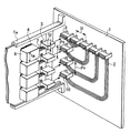
図4に示すように、本実施形態の情報処理装置は、筐体31内に複数の回路基板4が収容され、この複数の回路基板4は略直角に光バックプレーン1に配置される。回路基板4には、回路基板側の光コネクタ5と光電変換モジュール6が設けられ、光バックプレーン1には光バックプレーン側の光コネクタ3が設けられている。光コネクタ3と光コネクタ5とは光学的に接続される。情報処理装置としては、例えば、ルータ、サーバ等がある。
As shown in FIG. 4, in the information processing apparatus according to the present embodiment, a plurality of
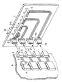
図1に示すように、光バックプレーン1上に複数の光ファイバ2を並べて敷線したものをシート状にして貼り付け、平行に並べた光ファイバ2の端末部分を、光ファイバ端からの光線入出射方向が光バックプレーン1の主面に対して略直角になるように曲げて、光コネクタ3を取り付ける。光コネクタ3は複数の光ファイバ2の端部を配列して収容することになる。これにより、あるボード(回路基板となる)と別のボードに対応する光コネクタ同士が光ファイバ2によって光配線される。このとき、光バックプレーン1側の光コネクタ3の光ファイバ配列方向は回路基板となるボード4の主面に対して略直角となるように光コネクタ3を設置する。
As shown in FIG. 1, a plurality of
一方、ボード4の端部には複数の光ファイバを並べて収容した光コネクタ5を設置し、このときボード側の光コネクタ5の光ファイバ配列方向はボード4の主面に対して略直角となるように光コネクタ5を設置する。ボード側光コネクタ5と光電変換モジュール6とは光ファイバアレイ7によって接続される。光バックプレーン1にはガイド1aが取り付られ、ガイド1aに対してボード4を挿入すると同時に、光バックプレーン側の光コネクタ3とボード側の光コネクタ5とが光学的に接続される。なお、ここではガイド1aは一対のみ図1に図示されているが、光バックプレーン1に挿入するボードの枚数に対応したガイド1aが光バックプレーンに取付られる。図1に示した光バックプレーン1には、5枚のボードが取付けられる。図中左側のボードに4つの光コネクタ5が取付られて、ボードの主面に対して略平行に配列された(図中上下方向に配列された)、光バックプレーン1上の4つの光コネクタ3に、4つの光コネクタ5が接続される。残りのボードにそれぞれ光コネクタ5が1づつ取付られ、光バックプレーン1上の残りの4つの光コネクタ3にそれぞれ光コネクタ5が接続される。
On the other hand, an
本実施形態においては、光バックプレーン1側の光コネクタ3及びボード4側の光コネクタ5の光ファイバ配列方向がボード4の主面に対して略直角となるようにしている。しかし、略直角に限定されず、光コネクタ3及び光コネクタ5の光ファイバ配列方向がボード4の主面に対して非平行となるようにされていればよく、好ましくは光ファイバ配列方向がボード4の主面に対して45度〜135度、最も好ましくは略90度(略直角)であるとよい。光コネクタ5の光ファイバ配列方向がボード4の主面に対して非平行であれば、図15と図1との対比から明らかなように、従来の光コネクタ5の幅をt1としたとき、光コネクタ5の幅はt2(t2<t1)となるのでより、光コネクタ間ピッチを狭くして(ピッチP3<P1)、ボード4のコネクタ実装密度を上げることができる。
In the present embodiment, the optical fiber arrangement direction of the
また、光バックプレーン1においても光コネクタ3のボード4と略平行な方向のピッチを狭くすることができる(ピッチP4<P2)。さらに、図15では光コネクタ3はボード4の主面に対して略平行な状態なので、光コネクタ3間の光ファイバは2回曲げなければならないが、ボード4の主面に対して直角となるように傾けていけば、光コネクタ3間の光ファイバのコネクタ部分の迂回部8の曲げを少なくすることができ、光ファイバの曲げに必要な距離を小さくすることができるので(45度〜135度とすれば光ファイバの迂回部8の曲げに必要な光コネクタ3間の距離がほとんどなくなり、略90度ではコネクタ部分の迂回部8の曲げそのものをなくすことができる)、光コネクタ3のボード4の主面と直角な方向のピッチをも狭くすることができる(ピッチl2<l1)。
Also in the
本実施形態においては、光電変換モジュール6の光ファイバ配列方向もボード4の主面に対して略直角となるように配置している。こうすることで、光電変換モジュール6の幅を小さくでき、ボード4の実装密度をさらに上げることができるので構成上望ましい。なお、光電変換モジュール6の光ファイバ配列方向のボード4の主面に対する角度が、光コネクタ5の光ファイバ配列方向のボード4の主面に対する角度と異なると光ファイバアレイ7のねじれが生ずるので、同じ角度(光ファイバ配列方向が同一方向)であることが望ましいが、必ずしも角度が同じでなくてもよい。例えば、光ファイバアレイ7のねじれの許容範囲で両者の角度を変えてもよく、光電変換モジュール6と光コネクタ5との間の距離が取れ、光ファイバアレイ7のねじれや曲げが許容される場合には両者の角度を任意に変えてもよい。
In the present embodiment, the optical fiber arrangement direction of the
例えば、光コネクタ5の光ファイバ配列方向がボード4の主面に対して略直角であっても、光電変換モジュール6と光コネクタ5との間の距離を取れ、光ファイバアレイ7のねじれや曲げが許容される場合には光電変換モジュール6の光ファイバ配列方向がボード4の主面に対して平行であってもよい。また後述する第4の実施形態の図16に示すように、光コネクタ5の光ファイバ配列方向がボード4の主面に対して略平行である場合には、光電変換モジュール6と光コネクタ5との間の距離を取れ、光ファイバアレイ7のねじれや曲げが許容される場合には光電変換モジュール6の光ファイバ配列方向がボード4の主面に対して、非平行(略直角である場合も含む)であってもよい。
For example, even if the optical fiber array direction of the
ボード4の実装密度を上げるには、光電変換モジュール6の光ファイバ配列方向をボード4の主面に対して略直角となるように配置しなくても、光電変換モジュール6の光ファイバ配列方向がボード4の主面に対して非平行となるようにされていればよく、好ましくは光ファイバ配列方向がボード4の主面に対して45度〜135度、最も好ましくは略90度(略直角)であるとよい。非平行であれば、図15と図1との対比から明らかなように、従来の光電変換モジュール6の幅をt3としたとき、光電変換モジュール6の幅はt4(t4<t3)となるので、その幅を小さくでき、ボード4の実装密度を上げることができる。
In order to increase the mounting density of the
光電変換モジュール6の光ファイバ配列方向はボード4の主面に対して略直角となるように配置されているが、このような光電変換モジュールはボード4への取付面に対して光電変換チップを略直角になるように配置して光電変換モジュール内に収容することで作成することができる。光電変換チップは発光素子又は/及び受光素子を備えたチップである。
The optical fiber array direction of the
このように光コネクタの幅t2、ピッチP3,P4、及びピッチl2を小さくすることができるので、図2に示すように、ボード4における光コネクタ5の実装密度、及び光バックプレーン1における光コネクタ3の実装密度を高くして、搭載できる光コネクタ5、光コネクタ3の数を増すことができる。
また、本実施形態において、光コネクタの光ファイバー配列は一列として示したが、二列以上としてもよい。
Since the width t2, the pitches P3 and P4, and the pitch l2 of the optical connector can be reduced in this way, the mounting density of the
Moreover, in this embodiment, although the optical fiber arrangement | sequence of the optical connector was shown as one row, it is good also as two or more rows.
本実施形態に係わる光伝送方法について、図1、図3を用いて説明する。図3は光伝送方法のフローを示す図である。 The optical transmission method according to this embodiment will be described with reference to FIGS. FIG. 3 is a diagram showing a flow of the optical transmission method.
光バックプレーン1に二つの回路基板(ボード)4,4′が取り付られ、一方の回路基板4上に設けられた光電変換モジュール6により電気信号が光信号に光電変換され(ステップS11)、回路基板4に対して非平行に光信号が並行に出力され、回路基板4上の光コネクタ5、光バックプレーン1上の光コネクタ3を介して光バックプレーン1に送られる(ステップS12、S13)。この光コネクタ3は光バックプレーン1上の他の光コネクタ3′に複数の光ファイバ2を介して接続され、光信号が他のコネクタ3′に送られる(ステップS14)。光バックプレーン1上の他のコネクタ3′、他の回路基板4′上に設けられた光コネクタ5′を介して、他の回路基板4′に対して非平行に光信号が並行に送られ(ステップS15)、他の回路基板4′の光電変換モジュール6′で光信号が電気信号に光電変換される(ステップS16)。
[第2の実施形態]
図5は本発明による光バックプレーンを用いた情報処理装置における回路基板と光バックプレーンの接続部を示す斜視図である。図5において、図1の構成部材と同一構成部材については同一符号を付して説明を省略する。回路基板となるボード4の端部には光コネクタ3と接続可能な光インタフェース11を備えた光電変換モジュール6を塔載し、光電変換モジュール6の光インタフェース11の光入出射ポートの配列方向はボード4の主面と略直角とする。光バックプレーン1のガイド1a(図5においてガイド1aは不図示)にボード4を挿入すると同時に、光バックプレーン側光コネクタ3とボード4側に搭載した光電変換モジュール6の光インタフェース11とが光学的に接続される。光電変換モジュール6が光インタフェース11を備える点以外の構造は第1の実施形態と同様である。
Two circuit boards (boards) 4 and 4 ′ are attached to the
[Second Embodiment]
FIG. 5 is a perspective view showing a connection portion between a circuit board and an optical backplane in an information processing apparatus using the optical backplane according to the present invention. In FIG. 5, the same components as those in FIG. A
本実施形態では第1の実施形態の効果に加えて、ボード上で光コネクタと光電変換モジュールとを接続する光ファイバがないので、ボード上の実装密度をより高くすることができる。
[第3の実施形態]
図6(a)〜(c)は本発明による光バックプレーンを用いた情報処理装置における回路基板と光バックプレーンの接続部を示す図である。図6(a)はボード上面より見た本構成の断面分解図、図6(b)は光バックプレーン表面から見た図、図6(c)はボードを光バックプレーンに挿入した状態を、ボード上面から見た断面図である。本実施形態の情報処理装置の全体構成は、回路基板に光電変換モジュールが搭載されておらず、電気コネクタが回路基板に配置され、光電変換モジュールが光バックプレーン側の電気コネクタ内に設けられ、その光電変換モジュールが直接光バックプレーン側の光コネクタと接続されている点が第1の実施形態と異なる。情報処理装置における、回路基板、光バックプレーン、筐体の配置関係は図4に示した構成と同じである。直接光バックプレーン側の光コネクタの光ファイバ2の敷線は図1の配置と同様である。
In the present embodiment, in addition to the effects of the first embodiment, since there is no optical fiber for connecting the optical connector and the photoelectric conversion module on the board, the mounting density on the board can be further increased.
[Third Embodiment]
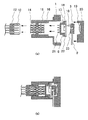
FIGS. 6A to 6C are diagrams showing a connection portion between a circuit board and an optical backplane in an information processing apparatus using the optical backplane according to the present invention. 6A is a cross-sectional exploded view of the present configuration seen from the top surface of the board, FIG. 6B is a view seen from the surface of the optical backplane, FIG. 6C is a state where the board is inserted into the optical backplane, It is sectional drawing seen from the board upper surface. In the overall configuration of the information processing apparatus of the present embodiment, the photoelectric conversion module is not mounted on the circuit board, the electrical connector is disposed on the circuit board, the photoelectric conversion module is provided in the electrical connector on the optical backplane side, The difference from the first embodiment is that the photoelectric conversion module is directly connected to the optical connector on the optical backplane side. The arrangement relationship of the circuit board, the optical backplane, and the housing in the information processing apparatus is the same as that shown in FIG. The laying line of the
図7はボード側の電気コネクタ、光バックプレーン側の電気コネクタ、光電変換モジュールの分解斜視図、図8は光コネクタと光バックプレーンの分解斜視図である。 FIG. 7 is an exploded perspective view of the electrical connector on the board side, the electrical connector on the optical backplane side, and the photoelectric conversion module, and FIG. 8 is an exploded perspective view of the optical connector and the optical backplane.
複数の光ファイバ2を並べて敷線した光バックプレーン1に光バックプレーンコネクタとなる電気コネクタ16を設ける。ここでは図示していないが、図1と同様に、光バックプレーンにはガイド1aが設けられ、光バックプレーン1の主面に対して略直角方向にボード4を挿抜可能とする。電気コネクタ16内部には、光電変換モジュール6を収容する。光バックプレーン側の電気コネクタ16は外側電気接点14と、内側電気接点15を備える。外側電気接点14はボード4に設けた電気コネクタ12の電気接点13と電気的に接続するためのものであり、内側電気接点15は光電変換モジュール6の電気接点21と電気的に接続するためのものである。光電変換モジュール6の入出射光は光バックプレーン1に対して略直角となるようにする。電気コネクタ16には、光電変換モジュール6が嵌合可能なように光電変換モジュール6の形状に合った凹部が形成され、光電変換モジュール6が収容可能となっている。そして凹部内(ここでは凹部の底部)に内側電気接点15が設けられ、凹部に光電変換モジュール6を挿入することで、電気コネクタ16の内側電気接点15と光電変換モジュール6の電気接点21とが電気的接続される。
An
図7に示すように、光バックプレーンコネクタとなる電気コネクタ16の光バックプレーン取付部16Aの一部には二箇所切り込みが設けられおり、電気コネクタ16に嵌入された光電変換モジュール6の光透過性基板22がこの切り込み部分に露出するので、この光透過性基板22を掴んで電気コネクタ16から光電変換モジュール6を取り出すことができ、光電変換モジュール6を取り出しやすいようになっている。光電変換モジュール6の入出射光は光バックプレーン1に対して略直角となるようにする。入出射光を光バックプレーン1に対して略直角とすることで、光電変換モジュール6を光コネクタ3に嵌合させる際の押し込み量ばらつきが光軸ずれに与える影響を小さくすることができる。
As shown in FIG. 7, two cuts are provided in a part of the optical
光電変換モジュール6と回路基板側のコネクタ13との間は電気接点21、15、14および13により高速電気配線接続される。
The
光電変換モジュール6の光透過性基板22には光コネクタ3に設けられたガイドピン10と嵌合するための嵌合穴18を設ける。光電変換モジュール6の電気接点21と電気コネクタ16の内側電気接点15との接触および導通は、内側電気接点15の弾性力によって保持される。この構造により光電変換モジュール6が故障した場合でも電気コネクタ16を取り外して光電変換モジュール6を容易に交換できるため、保守性が良好である。
光電変換モジュール6を交換するには、回路基板4を電気コネクタ16より抜去し、電気コネクタ16を光バックプレーン1より取り外す。次に内部に収容されている光電変換モジュール6を取り出し、新たな光電変換モジュールを収容する。ここでは、光バックプレーンコネクタとなる電気コネクタ16は光バックプレーン1にねじ止めされており、このねじを外すことで電気コネクタ16を光バックプレーン1から取り外す。
The
In order to replace the
光バックプレーン1上の光ファイバ2の端部には光路変換手段となる45度ミラー23、ガイドピン10を備えた光コネクタ3を取り付ける。光コネクタ3のガイドピン10と光電変換モジュール6側の嵌合穴18とを嵌合させることにより位置決めを達成する。光電変換モジュール6内の光素子(受光素子、発光素子、又は受光素子と発光素子)17と光ファイバ2とは光コネクタ3内の45度ミラー23を介して光学的に結合する。光素子17は光コネクタ3からの光を受光して電気信号に変換し、又は/及びボード4からの電気信号を光信号に変換する。45度ミラーを介して結合することで、ファイバ直角立ち上げにおいてもファイバ曲げが不要となり、光ファイバ曲げによる光路変換で問題となる曲げ半径の限界に関係なく、コネクタ同士の間隔を詰めて、狭ピッチでの光コネクタ配置が可能となる。光素子17は半導体基板に設けられ、この半導体基板は光透過性基板22上に設けられ、光透過性基板22上は光素子17を覆うように、凸形状をなすモジュール本体が設けられている。モジュール本体上に電気接点21が設けられている。
At the end of the
光コネクタ3と光バックプレーン1の間にはバネ19が入っており、光電変換モジュール6と光コネクタ3との物理的な接触がバネ19の弾性力によって保持される。これにより光電変換モジュールと光伝送路との間に余計な隙間が生じて結合効率が不安定になることを防げる。
光コネクタ3と光バックプレーン1の間には弾性体が挿入されていればよく、バネの他にスプリング、ゴムシート、板バネ、ウレタン等を用いることができる。
A
An elastic body may be inserted between the
本実施形態に係わる光伝送方法について図9を用いて説明する。
光バックプレーン1に二つの回路基板4,4′が取り付られ、一方の回路基板4上に設けられた回路により信号処理された電気信号が、回路基板4上の電気コネクタ12から出力され(ステップS21)、光バックプレーン1に取り付られた電気コネクタ16内の光電変換モジュール6に入力されて光信号に光電変換される(ステップS22)。光信号は回路基板4に対して非平行に光コネクタ3に並行に出力され、光ファイバを介して他の光コネクタ3′を介して他の電気コネクタ16′内の光電変換モジュール6′に送られ、光信号が電気信号に光電変換される(ステップS23)。光電変換された電気信号は、光バックプレーン1の他の電気コネクタ16′と接続される、他の回路基板4′の電気コネクタ12′に送られ、他の回路基板4′で信号処理される(ステップS24)。
The optical transmission method according to this embodiment will be described with reference to FIG.
Two
以上説明した構成では、光電変換モジュールに一つの光素子を収納する場合について説明したが、本実施形態において、図10に示すように光電変換モジュールに二つの光素子を収納してもよい。 In the configuration described above, the case where one optical element is accommodated in the photoelectric conversion module has been described. However, in this embodiment, two optical elements may be accommodated in the photoelectric conversion module as shown in FIG.
光電変換モジュール6には二つの光素子17を収容し、光コネクタ3に二つの45度ミラーを設けてそれぞれ異なる方向へ伸びる光ファイバ2に結合するようにする。光電変換モジュール6側の嵌合穴18は光素子17間に設けられ、この嵌合穴18に光コネクタ3のガイドピン10が挿入される。このような実施形態により、例えばラックの中央付近に実装した回路基板となるスイッチ基板と左右双方に実装された回路基板となる信号入出力基板とを接続する場合などに、光バックプレーン上での光ファイバの引き回しを単純にでき、効率よく光相互接続することができる。図10では、説明をわかりやすくするために、光素子が二つで光ファイバ2が二本の場合を例として説明したが、光素子や光ファイバの数は3つ以上であっても構わない。
The
また本実施形態において、光バックプレーンにフタを設け、光電変換モジュールを光バックプレーン側から引き出せるようにしてもよい。 In the present embodiment, a lid may be provided on the optical backplane so that the photoelectric conversion module can be pulled out from the optical backplane side.
図11(a)はボード上面より見た本構成の断面分解図、図11(b)はボードを光バックプレーンに挿入した状態の、ボード上面から見た断面図である。また図12は光コネクタとフタの取付方法を示す図である。図11(a)、(b)及び図12において、図6及び図7と同一構成部材については同一符号を付して説明を省略する。 FIG. 11A is a cross-sectional exploded view of the present configuration viewed from the top surface of the board, and FIG. 11B is a cross-sectional view viewed from the top surface of the board with the board inserted into the optical backplane. FIG. 12 is a view showing a method of attaching the optical connector and the lid. 11A, 11B, and 12, the same components as those in FIGS. 6 and 7 are denoted by the same reference numerals, and description thereof is omitted.
光バックプレーンに貫通穴を設け、この貫通穴を塞ぐフタ20を設ける。フタ20を開け、光コネクタ3のガイドピン10を光電変換モジュール6の嵌合穴18から抜いて光バックプレーン1の後ろに引き出すことにより光電変換モジュール6を光バックプレーン後ろに取り出すことができる。この構造により光電変換モジュールが故障した場合などにボード4を抜かずに装置を駆動したまま容易に取り外し交換ができるため、さらに保守性が良好である。フタ20は光バックプレーンに取付られた扉でもよい。
A through hole is provided in the optical backplane, and a
また、本実施形態において、光バックプレーンコネクタとなる電気コネクタは2つ以上の構成部に分割可能な構成としてもよい。このような構成においても、光電変換モジュールを内部に収容することができる。 In the present embodiment, the electrical connector serving as the optical backplane connector may be divided into two or more components. Even in such a configuration, the photoelectric conversion module can be accommodated inside.
図13に電気コネクタの断面図、図14にその斜視図を示す。図13及び図14に示すように、電気コネクタ16を2つの構成部16−1と16−2とに分割可能とし、構成部16−2に光電変換モジュールを挿入した後に構成部16−2を構成部16−1に嵌入して、構成部16−1の電気接点と光電変換モジュールの電気接点とを接続する、又は構成部16−1に光電変換モジュールを挿入した後に構成部16−2を構成部16−1内に嵌入する。この場合、構成部16−1に端部に凸部を有する爪部(ここでは2箇所爪部を設けている)16−1Aを設け、構成部16−2にそれを受ける凹部16−2Aを設けることで、両者を固定接続することができる。構成部16−2に爪部を設け、構成部16−1にそれを受ける凹部を設けることで、両者を固定接続することもできる。また、構成部16−2を構成部16−1に嵌入するのではなく、構成部16−1を構成部16−2内に嵌入する構成としてもよい。
FIG. 13 is a sectional view of the electrical connector, and FIG. 14 is a perspective view thereof. As shown in FIGS. 13 and 14, the
このように、電気コネクタを2つの構成部16−1と16−2とに分割すれば、構成部16−2を光バックプレーンに固定した状態でも、構成部16−1を取り外して光電モジュールの交換が可能となる。 In this way, if the electrical connector is divided into two components 16-1 and 16-2, the component 16-1 can be removed and the photoelectric module of the photoelectric module can be removed even when the component 16-2 is fixed to the optical backplane. Exchange is possible.
以上説明した本実施形態の各構成では光電変換モジュール全体が光バックプレーンコネクタに収容される場合について説明したが、光電変換モジュールの一部(例えば透明基板22の部分)が電気コネクタに収容されず、光バックプレーン側に入り込むようにしてもよい。 In each configuration of the present embodiment described above, the case where the entire photoelectric conversion module is accommodated in the optical backplane connector has been described. However, a part of the photoelectric conversion module (for example, the transparent substrate 22) is not accommodated in the electrical connector. Alternatively, the light may enter the optical backplane side.
また本実施形態において、電気コネクタ16の凹部に嵌入される光電変換モジュールの凸部の形状は、光電変換モジュールの一部の凸部が凹部の一部に嵌るようにされるように構成されていてもよい。例えば、図6に示す光電変換モジュールの透明基板22を含む部分は、電気コネクタ16の第1の凹部16Aに嵌るように形成され第1の凹部16Aに嵌合するが、電気接点21を有する部分は電気コネクタ16の第2の凹部16B(第1の凹部の奥の凹部で、第1の凹部よりも小さい)よりも小さく形成され、第2の凹部16Bに嵌らないように形成されてもよい。
Moreover, in this embodiment, the shape of the convex part of the photoelectric conversion module inserted into the concave part of the
また本実施形態において、光コネクタ3は光電変換モジュール6に接するように配置されなくてもよく、光電変換モジュール6を電気コネクタ16に挿入した後に、開口部を有するフタ又は電気コネクタ16に取り付られた扉で蓋をし、このフタや扉上に光コネクタ3を取り付けてもよい。
In the present embodiment, the
さらに、本実施形態において、電気コネクタの内部に光電変換モジュールを収容可能であればよいので、必ずしも光電変換モジュールは電気コネクタ16の凹部に嵌合しなくともよい。例えば、電気接点15と電気接点21との接続で十分に接続の信頼性が保てれば、光電変換モジュールは電気コネクタ16の凹部に嵌入されるような凸形状を有する必要はなく、電気コネクタ16の凹部の内壁に光電変換モジュールが接していなくてもよい。
また、図7、図8、図12においては、ガイドピン10もしくは嵌合穴18と、光入出射部24とが一直線上に配置されていないが、これらは一直線上に配置されていても良い。
また、以上の説明では、電気接点15が電気接点21を挟み込む構造として説明をしてきたが、逆に、電気接点21が電気接点15を挟み込む構造としてもよい。
Furthermore, in the present embodiment, it is sufficient that the photoelectric conversion module can be accommodated inside the electrical connector, and therefore the photoelectric conversion module does not necessarily have to be fitted into the recess of the
In FIGS. 7, 8, and 12, the
In the above description, the
[第4の実施形態]
図16は本発明による光バックプレーンを用いた情報処理装置における回路基板と光バックプレーンの接続部を示す斜視図である。図16において、図1及び図15の構成部材と同一構成部材については同一符号を付して説明を省略する。
[Fourth Embodiment]
FIG. 16 is a perspective view showing a connection portion between a circuit board and an optical backplane in an information processing apparatus using the optical backplane according to the present invention. In FIG. 16, the same components as those in FIGS. 1 and 15 are denoted by the same reference numerals, and the description thereof is omitted.
本実施形態は、ボード4の主面と略平行な方向に配列した複数の光コネクタ3−1の光ファイバ配列方向は図15の光コネクタ3と同様にボード4の主面に対して略平行であるが、ボード4の主面と略直角な方向に配列した複数の光コネクタ3−2の光ファイバ配列方向は図1の光コネクタ3と同様にボード4の主面に対して非平行(ここでは略直角となっている)としている。図16に示した光バックプレーン1には、5枚のボードが取付けられる。図中左側のボードに4つの光コネクタ5が取付られて、ボードの主面に対して略平行に配列された(図中上下方向に配列された)、光バックプレーン1上の4つの光コネクタ3−1に4つの光コネクタ5が接続される。残りのボードにそれぞれ光コネクタ5が1づつ取付られ、光バックプレーン1上の残りの4つの光コネクタ3−2にそれぞれ光コネクタ5が接続される。
In the present embodiment, the optical fiber array direction of the plurality of optical connectors 3-1 arranged in a direction substantially parallel to the main surface of the
なお、ここでは、図中左側のボードに取付られる光コネクタ5の光ファイバ配列方向はボード4の主面に対して略平行となるが、残りのボードに取付られる光コネクタ5の光ファイバ配列方向はボード4の主面に対して非平行(ここでは略直角となっている)となる。
Here, the optical fiber arrangement direction of the
本実施形態では第1の実施形態と同様に、ボード4の主面と略直角な方向に配列した複数の光コネクタ3−2の光ファイバ配列方向は図1と同様にボード4の主面に対して非平行とすることで、図15に示すような光コネクタ3間の光ファイバのコネクタ部分の迂回部8の曲げを少なくすることができ、光ファイバの曲げに必要な距離を小さくすることができるので(45度〜135度とすれば光ファイバの迂回部8の曲げに必要な光コネクタ3間の距離がほとんどなくなり、略90度(略直角)ではコネクタ部分の迂回部8の曲げそのものをなくすことができる)、光コネクタ3のボード4の主面と略直角な方向のピッチをも狭くすることができる(ピッチl2<l1)。
In the present embodiment, as in the first embodiment, the optical fiber arrangement direction of the plurality of optical connectors 3-2 arranged in a direction substantially perpendicular to the main surface of the
なお、図16では光コネクタ3−2はボード4の主面に対して略直角方向に一列に配置されているが、光コネクタ3−2の配置は特に限定されず、任意に配置してもよい。すなわち、ボード4の主面に対して直角でない一定角度傾くように列状に複数の光コネクタ3−2を配置してもよく、また列状に複数の光コネクタ3−2を配置しなくてもよい。例えば光バックプレーン1の図中右端の光コネクタ3−2のみを光ファイバ2の長さを短くするために図中右下の位置に配置してもよい。これは本実施形態に限らず、実施形態1から3においても同様である。
In FIG. 16, the optical connectors 3-2 are arranged in a line in a direction substantially perpendicular to the main surface of the
1 光バックプレーン
2 光ファイバ
3 光バックプレーン側光コネクタ
4 ボード
5 ボード側光コネクタ
6 光電変換モジュール
7 ボード側光ファイバ
8 ファイバコネクタ迂回部
9 ファイバ直角立ち上げ部
10 ガイドピン
11 ボード側光電変換モジュール光インタフェース
12 ボード側電気コネクタ
13 ボード側電気コネクタ電気接点
14 光バックプレーン側電気コネクタ外側電気接点
15 光バックプレーン側電気コネクタ内側電気接点
16 光バックプレーン側電気コネクタ
17 光素子
18 嵌合穴
19 バネ
21 光電変換モジュール電気接点
22 光透過性基板
23 45度ミラー
24 光入出射部
DESCRIPTION OF
Claims (6)
前記回路基板から前記回路基板の主面と非平行に並行に送られる光信号を受ける又は前記回路基板へ前記回路基板の主面と非平行に並行に光を送る光コネクタを備え、該光コネクタは、複数の光ファイバの端部を配列して収容し、
前記光コネクタの前記光ファイバの配列方向は前記回路基板の前記主面と非平行であることを特徴とする光バックプレーン。 An optical backplane on which a circuit board is mounted at a substantially right angle,
An optical connector that receives an optical signal sent from the circuit board in parallel non-parallel to the main surface of the circuit board or sends light to the circuit board in parallel non-parallel to the main surface of the circuit board; Is arranged to accommodate the ends of a plurality of optical fibers,
An optical backplane, wherein the optical fiber array direction of the optical connector is non-parallel to the main surface of the circuit board.
前記回路基板の前記主面と略平行な方向に配された前記光コネクタと、前記回路基板の該主面と略直角な方向に配された前記光コネクタとが前記複数の光ファイバで接続されることを特徴とする光バックプレーン。 2. The optical backplane according to claim 1, wherein a plurality of the optical connectors are arranged in a direction substantially parallel to the main surface of the circuit board and a plurality of the optical connectors are arranged in a direction substantially perpendicular to the main surface of the circuit board. ,
The optical connector disposed in a direction substantially parallel to the main surface of the circuit board and the optical connector disposed in a direction substantially perpendicular to the main surface of the circuit board are connected by the plurality of optical fibers. An optical backplane characterized by that.
回路基板から前記回路基板の主面と略平行に並行に送られる光信号を受ける又は前記回路基板へ前記回路基板の主面と略平行に並行に光を送る第1光コネクタと、前記第1光コネクタと複数の光ファイバで接続される前記第2光コネクタと、を備え、
前記第1光コネクタは前記回路基板の前記主面と略平行な方向に複数配列され、
該第1及び第2の光コネクタは、前記複数の光ファイバの両端部をそれぞれ配列して収容し、
前記第1光コネクタの前記光ファイバの配列方向は前記回路基板の前記主面と略平行であり、前記第2光コネクタの前記光ファイバの配列方向は前記回路基板の前記主面と非平行であることを特徴とする光バックプレーン。 An optical backplane on which a circuit board is mounted at a substantially right angle,
A first optical connector that receives an optical signal sent from the circuit board in parallel with the main surface of the circuit board in parallel or sends light to the circuit board in parallel with the main surface of the circuit board; The second optical connector connected by an optical connector and a plurality of optical fibers,
A plurality of the first optical connectors are arranged in a direction substantially parallel to the main surface of the circuit board,
The first and second optical connectors are respectively arranged and accommodated at both ends of the plurality of optical fibers,
The arrangement direction of the optical fibers of the first optical connector is substantially parallel to the main surface of the circuit board, and the arrangement direction of the optical fibers of the second optical connector is non-parallel to the main surface of the circuit board. An optical backplane characterized by being.
Priority Applications (3)
| Application Number | Priority Date | Filing Date | Title |
|---|---|---|---|
| JP2005293768A JP4652204B2 (en) | 2005-10-06 | 2005-10-06 | Optical backplane and optical transmission method |
| US11/543,118 US7645075B2 (en) | 2005-10-06 | 2006-10-05 | Optical connection structure of optical backplane to circuit substrate |
| CN200610142113.0A CN100474016C (en) | 2005-10-06 | 2006-10-08 | Optical backplane and optical transmission method |
Applications Claiming Priority (1)
| Application Number | Priority Date | Filing Date | Title |
|---|---|---|---|
| JP2005293768A JP4652204B2 (en) | 2005-10-06 | 2005-10-06 | Optical backplane and optical transmission method |
Publications (2)
| Publication Number | Publication Date |
|---|---|
| JP2007102013A true JP2007102013A (en) | 2007-04-19 |
| JP4652204B2 JP4652204B2 (en) | 2011-03-16 |
Family
ID=38029009
Family Applications (1)
| Application Number | Title | Priority Date | Filing Date |
|---|---|---|---|
| JP2005293768A Expired - Fee Related JP4652204B2 (en) | 2005-10-06 | 2005-10-06 | Optical backplane and optical transmission method |
Country Status (3)
| Country | Link |
|---|---|
| US (1) | US7645075B2 (en) |
| JP (1) | JP4652204B2 (en) |
| CN (1) | CN100474016C (en) |
Cited By (4)
| Publication number | Priority date | Publication date | Assignee | Title |
|---|---|---|---|---|
| JP2007104487A (en) * | 2005-10-06 | 2007-04-19 | Nec Corp | Information processing apparatus, circuit board, photoelectric conversion module, and optical transmission method |
| WO2013128751A1 (en) * | 2012-03-02 | 2013-09-06 | 株式会社日立製作所 | Multi-channel optical module, and information processing device in which multi-channel optical module is used |
| JP2014112162A (en) * | 2012-12-05 | 2014-06-19 | Fujitsu Component Ltd | Optical connector, optical connector system, and optical backplane apparatus |
| US8992097B2 (en) | 2013-02-25 | 2015-03-31 | Japan Aviation Electronics Industry, Limited | Optical connector |
Families Citing this family (37)
| Publication number | Priority date | Publication date | Assignee | Title |
|---|---|---|---|---|
| JP2006053662A (en) * | 2004-08-10 | 2006-02-23 | Matsushita Electric Ind Co Ltd | Multiprocessor |
| US7527435B2 (en) * | 2007-03-29 | 2009-05-05 | Corning Cable Systems Llc | Right-angle optical fiber connector assembly |
| US7802927B2 (en) * | 2008-05-30 | 2010-09-28 | Corning Cable Systems Llc | Bent optical fiber couplers and opto-electrical assemblies formed therefrom |
| US8452148B2 (en) | 2008-08-29 | 2013-05-28 | Corning Cable Systems Llc | Independently translatable modules and fiber optic equipment trays in fiber optic equipment |
| US11294136B2 (en) | 2008-08-29 | 2022-04-05 | Corning Optical Communications LLC | High density and bandwidth fiber optic apparatuses and related equipment and methods |
| US9075216B2 (en) | 2009-05-21 | 2015-07-07 | Corning Cable Systems Llc | Fiber optic housings configured to accommodate fiber optic modules/cassettes and fiber optic panels, and related components and methods |
| DE20160489T1 (en) | 2009-06-19 | 2024-06-20 | Corning Optical Communications LLC | HIGH DENSITY AND BANDWIDTH OPTICAL FIBER DEVICES AND RELATED EQUIPMENT AND METHODS |
| US8992099B2 (en) | 2010-02-04 | 2015-03-31 | Corning Cable Systems Llc | Optical interface cards, assemblies, and related methods, suited for installation and use in antenna system equipment |
| US8913866B2 (en) | 2010-03-26 | 2014-12-16 | Corning Cable Systems Llc | Movable adapter panel |
| WO2011159387A1 (en) | 2010-04-16 | 2011-12-22 | Ccs Technology, Inc. | Sealing and strain relief device for data cables |
| US8879881B2 (en) | 2010-04-30 | 2014-11-04 | Corning Cable Systems Llc | Rotatable routing guide and assembly |
| US9075217B2 (en) | 2010-04-30 | 2015-07-07 | Corning Cable Systems Llc | Apparatuses and related components and methods for expanding capacity of fiber optic housings |
| US9519118B2 (en) | 2010-04-30 | 2016-12-13 | Corning Optical Communications LLC | Removable fiber management sections for fiber optic housings, and related components and methods |
| US9107294B2 (en) | 2010-07-26 | 2015-08-11 | Hewlett-Packard Development Company, L.P. | System including a module |
| US9279951B2 (en) | 2010-10-27 | 2016-03-08 | Corning Cable Systems Llc | Fiber optic module for limited space applications having a partially sealed module sub-assembly |
| AU2011336747A1 (en) | 2010-11-30 | 2013-06-20 | Corning Cable Systems Llc | Fiber device holder and strain relief device |
| CN103403594B (en) | 2011-02-02 | 2016-11-23 | 康宁光缆系统有限责任公司 | The optical backplane being suitable in equipment rack sets up the joints of optical fibre that cover of dense light valve and the assembly that optics connects |
| US9008485B2 (en) | 2011-05-09 | 2015-04-14 | Corning Cable Systems Llc | Attachment mechanisms employed to attach a rear housing section to a fiber optic housing, and related assemblies and methods |
| CN103649805B (en) | 2011-06-30 | 2017-03-15 | 康宁光电通信有限责任公司 | Fiber plant assembly of shell using non-U-width size and associated method |
| US8953924B2 (en) | 2011-09-02 | 2015-02-10 | Corning Cable Systems Llc | Removable strain relief brackets for securing fiber optic cables and/or optical fibers to fiber optic equipment, and related assemblies and methods |
| KR101498839B1 (en) * | 2011-09-28 | 2015-03-04 | 가부시키가이샤후지쿠라 | Cable Having Connector and Method for Manufacturing Cable Having Connector |
| WO2013071111A1 (en) * | 2011-11-09 | 2013-05-16 | Aurora Networks, Inc. | Blind mate optoelectronic device |
| US9038832B2 (en) | 2011-11-30 | 2015-05-26 | Corning Cable Systems Llc | Adapter panel support assembly |
| TWI487963B (en) * | 2012-04-08 | 2015-06-11 | Hon Hai Prec Ind Co Ltd | Surface laminar circuit (slc) interconnection system assembly |
| US9250409B2 (en) | 2012-07-02 | 2016-02-02 | Corning Cable Systems Llc | Fiber-optic-module trays and drawers for fiber-optic equipment |
| US9042702B2 (en) | 2012-09-18 | 2015-05-26 | Corning Cable Systems Llc | Platforms and systems for fiber optic cable attachment |
| ES2551077T3 (en) | 2012-10-26 | 2015-11-16 | Ccs Technology, Inc. | Fiber optic management unit and fiber optic distribution device |
| US8985862B2 (en) | 2013-02-28 | 2015-03-24 | Corning Cable Systems Llc | High-density multi-fiber adapter housings |
| US9804348B2 (en) * | 2013-07-04 | 2017-10-31 | Mellanox Technologies, Ltd. | Silicon photonics connector |
| US10146009B2 (en) | 2013-07-04 | 2018-12-04 | Mellanox Technologies, Ltd. | Silicon photonics connector |
| JP2015075730A (en) * | 2013-10-11 | 2015-04-20 | 日本航空電子工業株式会社 | Optical fiber with optical connector |
| GB2525657B (en) * | 2014-05-01 | 2018-01-31 | Xyratex Tech Limited | An optical connector assembly, an optical printed circuit board assembly, an insert, and a method of manufacturing an optical connector assembly |
| US9652429B2 (en) * | 2015-09-16 | 2017-05-16 | Onulas, Llc | Horizontally expandable computing system |
| CN107742786B (en) | 2017-10-13 | 2019-11-05 | 番禺得意精密电子工业有限公司 | The sub-assembly that electric connector combination is combined with optical fiber connector |
| CN116367017A (en) * | 2021-12-27 | 2023-06-30 | 华为技术有限公司 | An optical cross interconnect architecture and communication equipment |
| CN116953861A (en) * | 2022-04-15 | 2023-10-27 | 华为技术有限公司 | Optical back plate, manufacturing method thereof, optical back plate assembly and communication equipment |
| WO2024189599A1 (en) * | 2023-03-15 | 2024-09-19 | Te Connectivity Solutions Gmbh | Daughter-card optical backplane connector system |
Citations (5)
| Publication number | Priority date | Publication date | Assignee | Title |
|---|---|---|---|---|
| JP2002516493A (en) * | 1998-05-21 | 2002-06-04 | インターナショナル・ビジネス・マシーンズ・コーポレーション | Electronic card assembly |
| JP2003515785A (en) * | 1999-12-01 | 2003-05-07 | スリーエム イノベイティブ プロパティズ カンパニー | Fiber optic connector system |
| JP2004507785A (en) * | 2000-08-22 | 2004-03-11 | スリーエム イノベイティブ プロパティズ カンパニー | Fiber optic connector system |
| JP2005033683A (en) * | 2003-07-10 | 2005-02-03 | Fuji Xerox Co Ltd | Signal processing apparatus |
| US20060093272A1 (en) * | 2004-11-03 | 2006-05-04 | Fenwick David M | Optical connections and methods of forming optical connections |
Family Cites Families (2)
| Publication number | Priority date | Publication date | Assignee | Title |
|---|---|---|---|---|
| JPH11183749A (en) | 1997-12-22 | 1999-07-09 | Hitachi Chem Co Ltd | Optical circuit board and manufacture therefor |
| US20050047795A1 (en) * | 2003-08-28 | 2005-03-03 | Windover Lisa A. | Optical interconnect system and method of communications over an optical backplane |
-
2005
- 2005-10-06 JP JP2005293768A patent/JP4652204B2/en not_active Expired - Fee Related
-
2006
- 2006-10-05 US US11/543,118 patent/US7645075B2/en not_active Expired - Fee Related
- 2006-10-08 CN CN200610142113.0A patent/CN100474016C/en not_active Expired - Fee Related
Patent Citations (5)
| Publication number | Priority date | Publication date | Assignee | Title |
|---|---|---|---|---|
| JP2002516493A (en) * | 1998-05-21 | 2002-06-04 | インターナショナル・ビジネス・マシーンズ・コーポレーション | Electronic card assembly |
| JP2003515785A (en) * | 1999-12-01 | 2003-05-07 | スリーエム イノベイティブ プロパティズ カンパニー | Fiber optic connector system |
| JP2004507785A (en) * | 2000-08-22 | 2004-03-11 | スリーエム イノベイティブ プロパティズ カンパニー | Fiber optic connector system |
| JP2005033683A (en) * | 2003-07-10 | 2005-02-03 | Fuji Xerox Co Ltd | Signal processing apparatus |
| US20060093272A1 (en) * | 2004-11-03 | 2006-05-04 | Fenwick David M | Optical connections and methods of forming optical connections |
Cited By (5)
| Publication number | Priority date | Publication date | Assignee | Title |
|---|---|---|---|---|
| JP2007104487A (en) * | 2005-10-06 | 2007-04-19 | Nec Corp | Information processing apparatus, circuit board, photoelectric conversion module, and optical transmission method |
| US8322933B2 (en) | 2005-10-06 | 2012-12-04 | Nec Corporation | Optical connection structure between optical backplane and circuit substrate |
| WO2013128751A1 (en) * | 2012-03-02 | 2013-09-06 | 株式会社日立製作所 | Multi-channel optical module, and information processing device in which multi-channel optical module is used |
| JP2014112162A (en) * | 2012-12-05 | 2014-06-19 | Fujitsu Component Ltd | Optical connector, optical connector system, and optical backplane apparatus |
| US8992097B2 (en) | 2013-02-25 | 2015-03-31 | Japan Aviation Electronics Industry, Limited | Optical connector |
Also Published As
| Publication number | Publication date |
|---|---|
| CN1945368A (en) | 2007-04-11 |
| US7645075B2 (en) | 2010-01-12 |
| CN100474016C (en) | 2009-04-01 |
| JP4652204B2 (en) | 2011-03-16 |
| US20070086723A1 (en) | 2007-04-19 |
Similar Documents
| Publication | Publication Date | Title |
|---|---|---|
| JP4652204B2 (en) | Optical backplane and optical transmission method | |
| JP4858750B2 (en) | Information processing device | |
| KR101274547B1 (en) | Connection structure of photoelectric flexible wiring board, connector and photoelectric flexible wiring board | |
| US7486847B1 (en) | Chip carrier package with optical vias | |
| TWI668557B (en) | Server system | |
| US20090285580A1 (en) | Optical-Electrical Transceiver Module | |
| JP2006004921A (en) | Optical fiber transceiver module having rigid printed circuit board and flexible printed circuit board | |
| US9170386B2 (en) | Opto-electronic device assembly | |
| TW201404056A (en) | Plug and play optical transceiver module for electronic devices | |
| US7275876B2 (en) | Optical transmission circuit device | |
| JP4803459B2 (en) | Optical backplane connector, photoelectric conversion module, and optical backplane | |
| JP5655594B2 (en) | Optical transceiver | |
| JP5445026B2 (en) | Electric light composite harness | |
| EP1996969B1 (en) | Module having a plurality of circuit boards stacked with a prescribed distance therebetween and optical connector for the same | |
| CN216411657U (en) | an optical module | |
| TW201504707A (en) | Data center connector system using a straight-through cable assembly | |
| JP4344328B2 (en) | Photoelectric composite connector | |
| JP2004109324A (en) | Optical module | |
| JP3941578B2 (en) | Optical transmission device and optical data bus system | |
| WO2015087385A1 (en) | Optical wiring board, optical wiring board manufacturing method, and information processing apparatus using optical wiring board |
Legal Events
| Date | Code | Title | Description |
|---|---|---|---|
| RD04 | Notification of resignation of power of attorney |
Free format text: JAPANESE INTERMEDIATE CODE: A7424 Effective date: 20080523 |
|
| A711 | Notification of change in applicant |
Free format text: JAPANESE INTERMEDIATE CODE: A711 Effective date: 20080702 |
|
| A621 | Written request for application examination |
Free format text: JAPANESE INTERMEDIATE CODE: A621 Effective date: 20080715 |
|
| A521 | Request for written amendment filed |
Free format text: JAPANESE INTERMEDIATE CODE: A821 Effective date: 20080702 |
|
| A977 | Report on retrieval |
Free format text: JAPANESE INTERMEDIATE CODE: A971007 Effective date: 20100615 |
|
| A131 | Notification of reasons for refusal |
Free format text: JAPANESE INTERMEDIATE CODE: A131 Effective date: 20100621 |
|
| A521 | Request for written amendment filed |
Free format text: JAPANESE INTERMEDIATE CODE: A523 Effective date: 20100819 |
|
| A131 | Notification of reasons for refusal |
Free format text: JAPANESE INTERMEDIATE CODE: A131 Effective date: 20100906 |
|
| A521 | Request for written amendment filed |
Free format text: JAPANESE INTERMEDIATE CODE: A523 Effective date: 20101101 |
|
| TRDD | Decision of grant or rejection written | ||
| A01 | Written decision to grant a patent or to grant a registration (utility model) |
Free format text: JAPANESE INTERMEDIATE CODE: A01 Effective date: 20101202 |
|
| A01 | Written decision to grant a patent or to grant a registration (utility model) |
Free format text: JAPANESE INTERMEDIATE CODE: A01 |
|
| A61 | First payment of annual fees (during grant procedure) |
Free format text: JAPANESE INTERMEDIATE CODE: A61 Effective date: 20101215 |
|
| R150 | Certificate of patent or registration of utility model |
Free format text: JAPANESE INTERMEDIATE CODE: R150 |
|
| FPAY | Renewal fee payment (event date is renewal date of database) |
Free format text: PAYMENT UNTIL: 20131224 Year of fee payment: 3 |
|
| S531 | Written request for registration of change of domicile |
Free format text: JAPANESE INTERMEDIATE CODE: R313531 |
|
| S533 | Written request for registration of change of name |
Free format text: JAPANESE INTERMEDIATE CODE: R313533 |
|
| FPAY | Renewal fee payment (event date is renewal date of database) |
Free format text: PAYMENT UNTIL: 20131224 Year of fee payment: 3 |
|
| R350 | Written notification of registration of transfer |
Free format text: JAPANESE INTERMEDIATE CODE: R350 |
|
| LAPS | Cancellation because of no payment of annual fees |