JP2007073763A - Semiconductor device and manufacturing method thereof - Google Patents
Semiconductor device and manufacturing method thereof Download PDFInfo
- Publication number
- JP2007073763A JP2007073763A JP2005259655A JP2005259655A JP2007073763A JP 2007073763 A JP2007073763 A JP 2007073763A JP 2005259655 A JP2005259655 A JP 2005259655A JP 2005259655 A JP2005259655 A JP 2005259655A JP 2007073763 A JP2007073763 A JP 2007073763A
- Authority
- JP
- Japan
- Prior art keywords
- lead
- wire
- semiconductor device
- tip
- bonding
- Prior art date
- Legal status (The legal status is an assumption and is not a legal conclusion. Google has not performed a legal analysis and makes no representation as to the accuracy of the status listed.)
- Pending
Links
Images


Classifications
-
- H—ELECTRICITY
- H10—SEMICONDUCTOR DEVICES; ELECTRIC SOLID-STATE DEVICES NOT OTHERWISE PROVIDED FOR
- H10W—GENERIC PACKAGES, INTERCONNECTIONS, CONNECTORS OR OTHER CONSTRUCTIONAL DETAILS OF DEVICES COVERED BY CLASS H10
- H10W72/00—Interconnections or connectors in packages
- H10W72/071—Connecting or disconnecting
- H10W72/0711—Apparatus therefor
-
- H—ELECTRICITY
- H10—SEMICONDUCTOR DEVICES; ELECTRIC SOLID-STATE DEVICES NOT OTHERWISE PROVIDED FOR
- H10W—GENERIC PACKAGES, INTERCONNECTIONS, CONNECTORS OR OTHER CONSTRUCTIONAL DETAILS OF DEVICES COVERED BY CLASS H10
- H10W70/00—Package substrates; Interposers; Redistribution layers [RDL]
- H10W70/01—Manufacture or treatment
- H10W70/05—Manufacture or treatment of insulating or insulated package substrates, or of interposers, or of redistribution layers
- H10W70/093—Connecting or disconnecting other interconnections thereto or therefrom, e.g. connecting bond wires or bumps
-
- H—ELECTRICITY
- H10—SEMICONDUCTOR DEVICES; ELECTRIC SOLID-STATE DEVICES NOT OTHERWISE PROVIDED FOR
- H10W—GENERIC PACKAGES, INTERCONNECTIONS, CONNECTORS OR OTHER CONSTRUCTIONAL DETAILS OF DEVICES COVERED BY CLASS H10
- H10W72/00—Interconnections or connectors in packages
- H10W72/01—Manufacture or treatment
- H10W72/015—Manufacture or treatment of bond wires
- H10W72/01551—Changing the shapes of bond wires
-
- H—ELECTRICITY
- H10—SEMICONDUCTOR DEVICES; ELECTRIC SOLID-STATE DEVICES NOT OTHERWISE PROVIDED FOR
- H10W—GENERIC PACKAGES, INTERCONNECTIONS, CONNECTORS OR OTHER CONSTRUCTIONAL DETAILS OF DEVICES COVERED BY CLASS H10
- H10W72/00—Interconnections or connectors in packages
- H10W72/071—Connecting or disconnecting
- H10W72/0711—Apparatus therefor
- H10W72/07141—Means for applying energy, e.g. ovens or lasers
-
- H—ELECTRICITY
- H10—SEMICONDUCTOR DEVICES; ELECTRIC SOLID-STATE DEVICES NOT OTHERWISE PROVIDED FOR
- H10W—GENERIC PACKAGES, INTERCONNECTIONS, CONNECTORS OR OTHER CONSTRUCTIONAL DETAILS OF DEVICES COVERED BY CLASS H10
- H10W72/00—Interconnections or connectors in packages
- H10W72/071—Connecting or disconnecting
- H10W72/0711—Apparatus therefor
- H10W72/07178—Means for aligning
-
- H—ELECTRICITY
- H10—SEMICONDUCTOR DEVICES; ELECTRIC SOLID-STATE DEVICES NOT OTHERWISE PROVIDED FOR
- H10W—GENERIC PACKAGES, INTERCONNECTIONS, CONNECTORS OR OTHER CONSTRUCTIONAL DETAILS OF DEVICES COVERED BY CLASS H10
- H10W72/00—Interconnections or connectors in packages
- H10W72/071—Connecting or disconnecting
- H10W72/075—Connecting or disconnecting of bond wires
- H10W72/07521—Aligning
-
- H—ELECTRICITY
- H10—SEMICONDUCTOR DEVICES; ELECTRIC SOLID-STATE DEVICES NOT OTHERWISE PROVIDED FOR
- H10W—GENERIC PACKAGES, INTERCONNECTIONS, CONNECTORS OR OTHER CONSTRUCTIONAL DETAILS OF DEVICES COVERED BY CLASS H10
- H10W72/00—Interconnections or connectors in packages
- H10W72/071—Connecting or disconnecting
- H10W72/075—Connecting or disconnecting of bond wires
- H10W72/07531—Techniques
- H10W72/07532—Compression bonding, e.g. thermocompression bonding
- H10W72/07533—Ultrasonic bonding, e.g. thermosonic bonding
-
- H—ELECTRICITY
- H10—SEMICONDUCTOR DEVICES; ELECTRIC SOLID-STATE DEVICES NOT OTHERWISE PROVIDED FOR
- H10W—GENERIC PACKAGES, INTERCONNECTIONS, CONNECTORS OR OTHER CONSTRUCTIONAL DETAILS OF DEVICES COVERED BY CLASS H10
- H10W72/00—Interconnections or connectors in packages
- H10W72/50—Bond wires
-
- H—ELECTRICITY
- H10—SEMICONDUCTOR DEVICES; ELECTRIC SOLID-STATE DEVICES NOT OTHERWISE PROVIDED FOR
- H10W—GENERIC PACKAGES, INTERCONNECTIONS, CONNECTORS OR OTHER CONSTRUCTIONAL DETAILS OF DEVICES COVERED BY CLASS H10
- H10W72/00—Interconnections or connectors in packages
- H10W72/50—Bond wires
- H10W72/531—Shapes of wire connectors
- H10W72/536—Shapes of wire connectors the connected ends being ball-shaped
-
- H—ELECTRICITY
- H10—SEMICONDUCTOR DEVICES; ELECTRIC SOLID-STATE DEVICES NOT OTHERWISE PROVIDED FOR
- H10W—GENERIC PACKAGES, INTERCONNECTIONS, CONNECTORS OR OTHER CONSTRUCTIONAL DETAILS OF DEVICES COVERED BY CLASS H10
- H10W72/00—Interconnections or connectors in packages
- H10W72/50—Bond wires
- H10W72/531—Shapes of wire connectors
- H10W72/5363—Shapes of wire connectors the connected ends being wedge-shaped
-
- H—ELECTRICITY
- H10—SEMICONDUCTOR DEVICES; ELECTRIC SOLID-STATE DEVICES NOT OTHERWISE PROVIDED FOR
- H10W—GENERIC PACKAGES, INTERCONNECTIONS, CONNECTORS OR OTHER CONSTRUCTIONAL DETAILS OF DEVICES COVERED BY CLASS H10
- H10W72/00—Interconnections or connectors in packages
- H10W72/50—Bond wires
- H10W72/551—Materials of bond wires
- H10W72/552—Materials of bond wires comprising metals or metalloids, e.g. silver
- H10W72/5522—Materials of bond wires comprising metals or metalloids, e.g. silver comprising gold [Au]
-
- H—ELECTRICITY
- H10—SEMICONDUCTOR DEVICES; ELECTRIC SOLID-STATE DEVICES NOT OTHERWISE PROVIDED FOR
- H10W—GENERIC PACKAGES, INTERCONNECTIONS, CONNECTORS OR OTHER CONSTRUCTIONAL DETAILS OF DEVICES COVERED BY CLASS H10
- H10W72/00—Interconnections or connectors in packages
- H10W72/50—Bond wires
- H10W72/59—Bond pads specially adapted therefor
-
- H—ELECTRICITY
- H10—SEMICONDUCTOR DEVICES; ELECTRIC SOLID-STATE DEVICES NOT OTHERWISE PROVIDED FOR
- H10W—GENERIC PACKAGES, INTERCONNECTIONS, CONNECTORS OR OTHER CONSTRUCTIONAL DETAILS OF DEVICES COVERED BY CLASS H10
- H10W72/00—Interconnections or connectors in packages
- H10W72/90—Bond pads, in general
- H10W72/931—Shapes of bond pads
- H10W72/932—Plan-view shape, i.e. in top view
-
- H—ELECTRICITY
- H10—SEMICONDUCTOR DEVICES; ELECTRIC SOLID-STATE DEVICES NOT OTHERWISE PROVIDED FOR
- H10W—GENERIC PACKAGES, INTERCONNECTIONS, CONNECTORS OR OTHER CONSTRUCTIONAL DETAILS OF DEVICES COVERED BY CLASS H10
- H10W72/00—Interconnections or connectors in packages
- H10W72/90—Bond pads, in general
- H10W72/951—Materials of bond pads
- H10W72/952—Materials of bond pads comprising metals or metalloids, e.g. PbSn, Ag or Cu
-
- H—ELECTRICITY
- H10—SEMICONDUCTOR DEVICES; ELECTRIC SOLID-STATE DEVICES NOT OTHERWISE PROVIDED FOR
- H10W—GENERIC PACKAGES, INTERCONNECTIONS, CONNECTORS OR OTHER CONSTRUCTIONAL DETAILS OF DEVICES COVERED BY CLASS H10
- H10W74/00—Encapsulations, e.g. protective coatings
-
- H—ELECTRICITY
- H10—SEMICONDUCTOR DEVICES; ELECTRIC SOLID-STATE DEVICES NOT OTHERWISE PROVIDED FOR
- H10W—GENERIC PACKAGES, INTERCONNECTIONS, CONNECTORS OR OTHER CONSTRUCTIONAL DETAILS OF DEVICES COVERED BY CLASS H10
- H10W90/00—Package configurations
- H10W90/701—Package configurations characterised by the relative positions of pads or connectors relative to package parts
- H10W90/751—Package configurations characterised by the relative positions of pads or connectors relative to package parts of bond wires
- H10W90/756—Package configurations characterised by the relative positions of pads or connectors relative to package parts of bond wires between a chip and a stacked lead frame, conducting package substrate or heat sink
Landscapes
- Wire Bonding (AREA)
- Lead Frames For Integrated Circuits (AREA)
Abstract
【課題】 一次ボンディングにおけるボンディングパッドとボールとの接続信頼性および二次ボンディングにおけるリードとワイヤとの接続信頼性を向上できる技術を提供する。
【解決手段】 タブ14上に半導体チップ15を配置し、タブ14の周囲にインナーリード13を形成する。そして、インナーリード13の先端部(タブ14に近い側の先端部)13aに傾斜を設ける。半導体チップ15に形成されたボンディングパッド16とインナーリード13とをボール17およびワイヤ18を介して接続する。インナーリード13とワイヤ18とは、インナーリード13に設けられた傾斜した部分で圧着するようにする。インナーリード13に設けられた傾斜の角度は、例えば3度以上15度以下の範囲にする。
【選択図】 図5PROBLEM TO BE SOLVED: To provide a technique capable of improving the connection reliability between a bonding pad and a ball in primary bonding and the connection reliability between a lead and a wire in secondary bonding.
A semiconductor chip is disposed on a tab and inner leads are formed around the tab. The tip of the inner lead 13 (tip on the side close to the tab 14) 13a is inclined. The bonding pads 16 formed on the semiconductor chip 15 and the inner leads 13 are connected via balls 17 and wires 18. The inner lead 13 and the wire 18 are crimped at an inclined portion provided in the inner lead 13. The angle of inclination provided on the inner lead 13 is set to a range of 3 degrees to 15 degrees, for example.
[Selection] Figure 5
Description
本発明は、半導体装置およびその製造技術に関し、特に、リードフレームを使用する半導体装置およびその製造に適用して有効な技術に関するものである。 The present invention relates to a semiconductor device and a manufacturing technology thereof, and more particularly to a semiconductor device using a lead frame and a technology effective when applied to the manufacturing thereof.
特開平11−284017号公報(特許文献1)には、ワイヤボンディング時に発生するワイヤの離脱を防止可能とする技術が開示されている。具体的には、アイランドの周方に位置するリードの先端部が載置されるヒータプレートの先端縁部を、上りまたは下り勾配の傾斜状としている。 Japanese Patent Application Laid-Open No. 11-284017 (Patent Document 1) discloses a technique capable of preventing the detachment of a wire that occurs during wire bonding. Specifically, the leading edge portion of the heater plate on which the leading end portion of the lead located around the island is placed has an upward or downward slope.
特開平7−37940号公報(特許文献2)には、リード細線を外部リードに十分な機械的強度で固着できる技術が開示されている。具体的には、外部リードの一端に肉厚の押え部とこの押え部から突出する肉薄のポストを設ける。そして、押え部から突出するポストは、押え部の底面に対して傾斜するように構成するとしている。
半導体装置を製造する場合の一工程として、タブ上に配置された半導体チップとタブの周囲に配置されたリードとをワイヤを用いて電気接続する工程(ワイヤボンディング工程)がある。このワイヤボンディング工程では、金線からなるワイヤの先端を溶融して形成したボールを、半導体チップのボンディングパッド上に加熱圧着して、一次ボンディングを行なう。次に、ワイヤをリード上に移動した後、リードとワイヤとを加熱圧着して、二次ボンディングを行なう。このようにして、半導体チップ上のボンディングパッドとリードとをワイヤを用いて電気的に接続している。 As a process for manufacturing a semiconductor device, there is a process (wire bonding process) of electrically connecting a semiconductor chip arranged on a tab and a lead arranged around the tab using a wire. In this wire bonding step, primary bonding is performed by heat-pressing a ball formed by melting the tip of a wire made of a gold wire on a bonding pad of a semiconductor chip. Next, after the wire is moved onto the lead, the lead and the wire are thermocompression bonded to perform secondary bonding. In this way, the bonding pads on the semiconductor chip and the leads are electrically connected using the wires.
近年、半導体チップのサイズの縮小化に伴い、半導体チップ上に形成されているボンディングパッドの間隔も狭くなってきている。半導体チップとリードとをワイヤで接続する際には、図1に示すようなキャピラリ1と呼ばれるボンディング用ツールが使用されるが、ボンディングパッド間隔の縮小化に伴って、キャピラリ1の先端部1aのサイズも、隣接するボンディングパッドに干渉しないように縮小化する必要がある。
In recent years, with the reduction in the size of a semiconductor chip, the interval between bonding pads formed on the semiconductor chip has also been reduced. When connecting the semiconductor chip and the lead with a wire, a bonding tool called a
ところが、キャピラリ1の先端部1aを縮小化すると、リード上にワイヤを熱と超音波で圧着させる際、ワイヤの圧着面積が小さくなり、ワイヤの圧着強度の低下や剥がれが発生する問題点がある。つまり、リード上にワイヤを接続する二次ボンディングを行なう際の圧着強度が低下する問題点がある。
However, when the tip 1a of the
そこで、リードとワイヤとの圧着面積の縮小分を補うため、リードとワイヤとの圧着部の肉厚を厚くして圧着強度を上げることが考えられる。圧着部の肉厚を厚くするには、図2に示すキャピラリ1の先端部1aに角度αを持たせてあげることにより実現できる。また、半導体チップのサイズがより縮小化されても、キャピラリ1の先端部1aの角度αをより大きくすることで、更に圧着部の肉厚を厚くすることが可能である。
Therefore, in order to compensate for the reduction in the crimping area between the lead and the wire, it is conceivable to increase the crimping strength by increasing the thickness of the crimping part between the lead and the wire. Increasing the thickness of the crimping part can be realized by giving an angle α to the tip 1a of the
しかし、キャピラリ1の先端部1aの角度αを大きくしすぎると、図3に示すように、ボンディングパッド2上にボール3を圧着させる一次ボンディングの際、超音波およびボール3を押す荷重が、ボール3の外側に逃げてしまう。このため、ボンディングパッド2とボール3との境界において、ボール3の外周部は合金層(例えばAl−Au層)が形成されるのに対し、ボール3の中央部(キャピラリ1の先端部1aにおける開口部下)は合金層(例えばAl−Au層)が形成されにくくなる。したがって、ボンディングパッド2とボール3との境界全面に合金層が形成されないことから、ボンディングパッド2とボール3との接着強度が低下し、ボンディングパッド2からボール3が剥がれてしまう問題点がある。さらに、キャピラリ1の先端部1aの角度αを大きくしすぎると、キャピラリ1の先端部1aがくさびとして機能してしまい、二次ボンディングの際、リードと接続するワイヤをキャピラリ1の先端部1aで切断してしまうという問題も発生する。
However, if the angle α of the tip 1a of the
このような問題は、半導体チップの微細化により顕著となって現われる。例えば、ワイヤ径がφ=20μm以下になると、ワイヤのひっぱり強度が低下するため上述した問題が顕在化する。言い換えれば、ボンディングパッドの間隔が50μm以下になると問題が顕在化するとも言える。 Such a problem becomes prominent due to the miniaturization of semiconductor chips. For example, when the wire diameter is φ = 20 μm or less, the pulling strength of the wire decreases, and thus the above-described problem becomes apparent. In other words, it can be said that the problem becomes apparent when the bonding pad spacing is 50 μm or less.
本発明の目的は、一次ボンディングにおけるボンディングパッドとボールとの接続信頼性および二次ボンディングにおけるリードとワイヤとの接続信頼性を向上できる技術を提供することにある。 An object of the present invention is to provide a technique capable of improving the connection reliability between a bonding pad and a ball in primary bonding and the connection reliability between a lead and a wire in secondary bonding.
本発明の前記ならびにその他の目的と新規な特徴は、本明細書の記述および添付図面から明らかになるであろう。 The above and other objects and novel features of the present invention will be apparent from the description of this specification and the accompanying drawings.
本願において開示される発明のうち、代表的なものの概要を簡単に説明すれば、次のとおりである。 Of the inventions disclosed in the present application, the outline of typical ones will be briefly described as follows.
本発明による半導体装置の製造方法は、(a)半導体チップ上のボンディングパッドとリードの一先端部とを、先端がテーパ形状をしたキャピラリを用いてワイヤボンディングする工程を備え、前記(a)工程は、前記リードの一先端部が傾斜した状態で行なわれることを特徴とするものである。 A method of manufacturing a semiconductor device according to the present invention includes (a) wire bonding between a bonding pad on a semiconductor chip and one end of a lead using a capillary having a tapered tip. Is performed in a state where one end of the lead is inclined.
また、本発明による半導体装置は、(a)半導体チップと、(b)前記半導体チップの周囲に配置されたリードと、(c)前記半導体チップと前記リードの一先端部とを電気接続するワイヤと、(d)前記半導体チップ、前記リードおよび前記ワイヤを封止する樹脂とを備え、前記ワイヤが接続された前記リードの一先端部が傾斜しているものである。 The semiconductor device according to the present invention includes (a) a semiconductor chip, (b) a lead disposed around the semiconductor chip, and (c) a wire for electrically connecting the semiconductor chip and one end of the lead. And (d) a resin that seals the semiconductor chip, the lead, and the wire, and one end portion of the lead to which the wire is connected is inclined.
本願において開示される発明のうち、代表的なものによって得られる効果を簡単に説明すれば以下のとおりである。 Among the inventions disclosed in the present application, effects obtained by typical ones will be briefly described as follows.
リードの一先端部が傾斜した状態でワイヤボンディングするため、キャピラリの先端部の角度αを大きくすることなく、リードとワイヤとの圧着部の肉厚を厚くすることができる。したがって、キャピラリの先端部の角度αを大きくする必要がないので、一次ボンディングにおけるボンディングパッドとボールとの接続信頼性を向上させることができる。一方、リードの一先端部の傾斜とキャピラリの先端部の角度αを合わせた角度でリードとワイヤとを接続することができるので、リードとワイヤとの圧着部の肉厚を厚くすることができ、リードとワイヤとの接続信頼性を向上させることができる。 Since wire bonding is performed in a state where one tip portion of the lead is inclined, the thickness of the crimped portion between the lead and the wire can be increased without increasing the angle α of the tip portion of the capillary. Therefore, since it is not necessary to increase the angle α of the tip of the capillary, the connection reliability between the bonding pad and the ball in primary bonding can be improved. On the other hand, since the lead and the wire can be connected at an angle that combines the inclination of the tip of the lead and the angle α of the tip of the capillary, the thickness of the crimped portion between the lead and the wire can be increased. The connection reliability between the lead and the wire can be improved.
以下の実施の形態においては便宜上その必要があるときは、複数のセクションまたは実施の形態に分割して説明するが、特に明示した場合を除き、それらはお互いに無関係なものではなく、一方は他方の一部または全部の変形例、詳細、補足説明等の関係にある。 In the following embodiments, when it is necessary for the sake of convenience, the description will be divided into a plurality of sections or embodiments. However, unless otherwise specified, they are not irrelevant to each other. There are some or all of the modifications, details, supplementary explanations, and the like.
また、以下の実施の形態において、要素の数等(個数、数値、量、範囲等を含む)に言及する場合、特に明示した場合および原理的に明らかに特定の数に限定される場合等を除き、その特定の数に限定されるものではなく、特定の数以上でも以下でもよい。 Further, in the following embodiments, when referring to the number of elements (including the number, numerical value, quantity, range, etc.), especially when clearly indicated and when clearly limited to a specific number in principle, etc. Except, it is not limited to the specific number, and may be more or less than the specific number.
さらに、以下の実施の形態において、その構成要素(要素ステップ等も含む)は、特に明示した場合および原理的に明らかに必須であると考えられる場合等を除き、必ずしも必須のものではないことは言うまでもない。 Further, in the following embodiments, the constituent elements (including element steps and the like) are not necessarily indispensable unless otherwise specified and apparently essential in principle. Needless to say.
同様に、以下の実施の形態において、構成要素等の形状、位置関係等に言及するときは、特に明示した場合および原理的に明らかにそうではないと考えられる場合等を除き、実質的にその形状等に近似または類似するもの等を含むものとする。このことは、上記数値および範囲についても同様である。 Similarly, in the following embodiments, when referring to the shape, positional relationship, etc., of components, etc., unless otherwise specified, and in principle, it is considered that this is not clearly the case, it is substantially the same. Including those that are approximate or similar to the shape. The same applies to the above numerical values and ranges.
本発明の実施の形態を図面に基づいて詳細に説明する。なお、実施の形態を説明するための全図において、同一の部材には原則として同一の符号を付し、その繰り返しの説明は省略する。 Embodiments of the present invention will be described in detail with reference to the drawings. Note that components having the same function are denoted by the same reference symbols throughout the drawings for describing the embodiment, and the repetitive description thereof will be omitted.
(実施の形態1)
図4は、本実施の形態1における半導体装置の外観を示す斜視図である。本実施の形態1における半導体装置のパッケージ形態は、QFP(Quad Flat Package)である。図4に示すように、本実施の形態1における半導体装置10は、直方体の形状をした樹脂11で覆われており、この樹脂11の四側面からアウターリード12が突出している。アウターリード12は、L字型に曲げられた構造をしている。
(Embodiment 1)
FIG. 4 is a perspective view showing the appearance of the semiconductor device according to the first embodiment. The package form of the semiconductor device in the first embodiment is a QFP (Quad Flat Package). As shown in FIG. 4, the
図5は、図4のA−A線で切断した断面を示す断面図である。図5に示すように、リードは、樹脂11の側面から突出しているアウターリード12と樹脂11の内部に形成されているインナーリード13から構成されている。左右のインナーリード13で挟まれた(複数のインナーリード13で囲まれた)中央部には、タブ14が形成されており、このタブ14上に半導体チップ15が配置されている。半導体チップ15には、MISFET(Metal Insulator Semiconductor Field Effect Transistor)などの回路素子や配線が形成されており、最上層にボンディングパッド16が形成されている。ボンディングパッド16上には、ボール17を介してワイヤ18が接続されており、このワイヤ18はインナーリード13に接続されている。
FIG. 5 is a cross-sectional view showing a cross section taken along line AA of FIG. As shown in FIG. 5, the lead includes an
ここで、本発明の特徴の一つは、ワイヤ18を接続しているインナーリード13の先端部に傾斜を設けたことにある。これにより、ボンディングパッド16とボール17の接続信頼性を確保しながら、ワイヤ18とインナーリード13との接続信頼性を向上することができる。近年、半導体チップ15上に形成されたボンディングパッド16の狭ピッチ化が進められている。このため、ボンディングパッド16に接続するワイヤ18も細線化されている。ワイヤ18が細線化されると、ワイヤ18とインナーリード13との接続面積が小さくなり、ワイヤ18とインナーリード13との接着力が低下し、ワイヤ18がインナーリード13から剥がれる不良が発生しやすくなる。そこで、ボンディング用ツールであるキャピラリの先端部に角度をつけることが行なわれる。つまり、キャピラリの先端をテーパ形状にしている。このようにすることにより、ワイヤ18とインナーリード13の圧着部の肉厚を厚くすることができるので、接続信頼性を向上することができる。しかし、キャピラリの先端部に角度をつけすぎると、ボンディングパッド16とボール17との接続信頼性が悪くなる問題が発生する。なぜなら、超音波およびボール17を押す荷重が、ボール17の外側に逃げてしまうからである。ボール17を押す荷重がボール17の外側に逃げてしまうと、ボンディングパッド16とボール17との境界の中央部に合金層が形成されにくくなる。したがって、ボンディングパッド16とボール17との接着強度が低下し、ボンディングパッド16からボール17が剥がれやすくなる。このことから、キャピラリの先端部に角度をつけすぎることはできない。そこで、本実施の形態1では、インナーリード13の先端部13aに傾斜を設けている。これにより、キャピラリの先端部にそれほど角度をつけなくても、ワイヤ18とインナーリード13との圧着部の肉厚をかせげる。すなわち、ワイヤ18とインナーリード13とは、キャピラリの先端部に形成されている角度とインナーリード13の傾斜による角度をあわせた角度で圧着することができるので、圧着部の肉厚を厚くすることができ、ワイヤ18とインナーリード13との接続信頼性を向上させることができる。一方、キャピラリの先端部には、それほど角度がついていないので、ボンディングパッド16にボール17を押し付ける荷重が外側に逃げない。このため、ボンディングパッド16とボール17との接続信頼性を向上させることができる。つまり、本実施の形態1によれば、ボンディングパッド16とボール17との接続信頼性を確保しながら、ワイヤ18とインナーリード13との接続信頼性を向上することができる。
Here, one of the features of the present invention is that an inclination is provided at the tip of the
インナーリード13に設けられている傾斜は、インナーリード13の先端部13aにいくにつれてインナーリード13の厚さが薄くなるように形成されている。このように傾斜させることにより、ワイヤ18とインナーリード13との圧着部の肉厚をかせぐことができる。具体的にインナーリード13に設けられている傾斜の角度は、3度以上15度以下にすることが望ましい。インナーリード13に設けられている傾斜の角度が3度未満であると、圧着部の肉厚を充分にかせぐことができないからである。一方、インナーリード13に設けられている傾斜の角度が15度より大きくなると、キャピラリとインナーリード13との間の角度が大きくなりすぎて、キャピラリがくさびとして機能することになり、ワイヤ18が切断されるおそれがあるからである。ここで、キャピラリの先端部自体に形成されている角度は、ボンディングパッド16とボール17との接続性を考慮して、3度以上15度以下になっている。したがって、ワイヤ18とインナーリード13とを接続する際、キャピラリとインナーリード13との間に形成される角度は、キャピラリの先端部自体に形成された角度とインナーリード13の先端部に形成された傾斜の角度を合わせたものであり、6度以上30度以下になる。この角度の範囲であれば、圧着部の肉厚を充分かせげるとともに、キャピラリがくさびとして機能することによるワイヤ18の切断を防止することができる。このことから、インナーリード13の先端部13aに設けられている傾斜の角度は、3度以上15度以下にすることが望ましいことがわかる。
The inclination provided in the
インナーリード13の先端部13aに設けられている傾斜は、ワイヤ18とインナーリード13との圧着部の肉厚をかせいで接続信頼性の向上を図るために形成されているので、インナーリード13のうちワイヤ18と接続する領域に形成されていればよい。別の言い方をすれば、インナーリード13のうちワイヤ18と接続する領域には、例えば銀めっきが形成されているので、インナーリード13のうち銀めっきされている領域に傾斜が形成されていればよい。また、インナーリード13のうちワイヤ18と接続する領域は、例えば、インナーリード13の先端部から約500μmの範囲にあることから、インナーリード13の先端部から約500μmの範囲内の領域が傾斜していればよいとも言える。
The inclination provided at the
図6は、図4に示す半導体装置10の内部構造を示す上面図である。図6に示すように、半導体装置10の中央部には、タブ14が形成されており、タブ14の周囲には、リードが配置されている。リードは樹脂11で覆われているインナーリード13と樹脂で覆われていないアウターリード12より構成されている。タブ14上には、半導体チップ15が搭載されており、この半導体チップ15とインナーリード13とは、例えば金線などからなるワイヤ18で電気接続されている。
FIG. 6 is a top view showing the internal structure of the
次に、本実施の形態1における半導体装置の製造方法について図面を参照しながら説明する。 Next, a method for manufacturing the semiconductor device according to the first embodiment will be described with reference to the drawings.
まず、図7に示すように、リードフレームを用意する。リードフレームには、複数のリード21とリード21に囲まれた中央部にタブ20が形成されている。リード21の先端部のうちタブ20に近い側の先端部(一先端部)21aは、銀めっき22が施されているとともに、傾斜している。リードフレームは、タブ20やリード21などのパターンが、縦方向や横方向に繰り返し形成された構造となっており、複数個の半導体チップを搭載する多連構造をしている。
First, as shown in FIG. 7, a lead frame is prepared. The lead frame is formed with a plurality of
タブ20およびリード21よりなるリードフレームは、例えば、鉄とニッケルの合金あるいは銅などから形成されている。そして、リード21の先端部21aの上面には、ワイヤを良好にボンディングするため、めっき処理がなされて銀めっき22が形成されている。さらに、先端部21aの上面には傾斜が設けられている。この傾斜は、先端部21aの上面に設けられている一方、先端部21aの下面には設けられていない。すなわち、リード21の先端部21aは先端にいくにしたがって厚さが薄くなっている。先端部21aの下面に傾斜が設けられていないのは、先端部21aの下面にはワイヤをボンディングする必要がないので傾斜を設ける必要がなく、さらに、ステージ23上に隙間なくリードフレームを置けるように、リード21とタブ20の下面を水平に維持する必要があるからである。
The lead frame including the
このような構成を有するリードフレームは、例えば、プレス加工によって形成することができる。すなわち、型によるプレス加工により、タブ20とリード21を形成し、リード21の先端部21aに傾斜を設ける。その後、先端部21aにめっき法を使用して銀めっき22を形成することにより、図7に示すようなリードフレームを得ることができる。
A lead frame having such a configuration can be formed by, for example, pressing. That is, the
次に、図8に示すように、タブ20上に半導体チップ24を搭載する。タブ20と半導体チップ24とは、例えば、Auペーストやエポキシ樹脂系の接着剤を用いて接着される。半導体チップ24は、半導体ウェハの状態でMISFETや配線が形成され、その後、ダイシングで半導体ウェハを個片化することにより得られる。なお、半導体チップ24の上面には、例えば、アルミニウムよりなるボンディングパッド25が形成されている。
Next, as shown in FIG. 8, the
続いて、図9に示すように、半導体チップ24上のボンディングパッド25とリード21とをボール26およびワイヤ27を介して電気接続する。このとき、リード21は、押え冶具28により固定されている。この押え冶具28は、リード21のうち銀めっき22が施されている領域よりも外側の領域を押えるようになっている。これは、銀めっき22を施されている領域を押えるようにすると、押え治具28が汚れてしまうからである。そして、ボンディングパッド25とリード21とを接続するボール26およびワイヤ27は、ボンディング用ツールであるキャピラリ29を用いて形成される(ワイヤボンディング工程)。
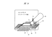
Subsequently, as shown in FIG. 9, the
以下に、上述したワイヤボンディング工程の詳細について説明する。まず、図10に示すように、キャピラリ29を用いてボール26を形成する。キャピラリ29には、超音波を伝達する超音波ホーン30が取り付けられているとともに、キャピラリ29の内部に金線31が形成されている。この金線31をキャピラリ29の先端部から取り出す。そして、キャピラリ29の先端部から出ている金線31に、放電トーチ32を接触させて金線31の先端部に球状のボール26を形成する。
Below, the detail of the wire bonding process mentioned above is demonstrated. First, as shown in FIG. 10, a
次に、図11に示すように、金線31の先端部に形成したボール26を、半導体チップ24に形成されたボンディングパッド25上に押し付ける(一次ボンディング)。このときの様子を図12に示す。図12に示すように、ボンディングパッド25上に金線31の先端部に形成されたボール26を、キャピラリ29を用いて押し付ける。ここで、図12に示すように、キャピラリ29の先端部に形成された角度αは大きくないため、キャピラリ29によってボール26を押し付けた荷重および超音波は外側に逃げない。したがって、ボール26の中央部に荷重が充分にかかるため、ボンディングパッド25とボール26の境界の中央部に合金層が形成される。例えば、ボンディングパッド25は、アルミニウムから形成され、ボール26は金から形成されているため、境界にアルミニウムと金からなる合金層が形成される。これにより、ボンディングパッド25とボール26の接着力を向上させることができるので、ボール26がボンディングパッド25から剥がれ落ちることを防止することができる。キャピラリ29の先端部に形成された角度αは、キャピラリ29によってボール26に押し付けた荷重が外側に逃げないのに充分な範囲で設定されており、例えば3度から15度の範囲で形成されている。キャピラリ29によってボール26に押し付けた荷重が外側に逃げないようにする観点からは、キャピラリ29の先端部に形成された角度αは0度であることが望ましい。一方、後述するように、リード21とワイヤ27を接続する際、圧着部の肉厚をかせいで接着力を向上させる観点から、キャピラリ29の先端部に角度αを形成することが望ましい。そこで、本実施の形態1では、キャピラリ29によってボール26に押し付けた荷重および超音波が極力外側に逃げない範囲で、キャピラリ29の先端部に角度αを設けている。ただし、キャピラリ29の先端部に設けられた角度αは、ボンディングパッド25とボール26の接着力(一次ボンディングの接着力)を向上することを考慮して、小さくなっているので、ワイヤ27とリード21との接着の際における肉厚をかせぐ点を充分に考慮した大きさの角度αが設定されているとはいえない。
Next, as shown in FIG. 11, the
次に、図13に示すように、ボール26からリード21へ向かってワイヤ27を形成する(ルーピング)そして、図14に示すように、ボール26から延在するワイヤ27をリード21の先端部近傍(インナーリード側)に接続する(ステッチボンド、二次ボンディング)。このとき、ワイヤ27を接続するリード21には傾斜が形成されている。図15は、ワイヤ27を銀めっき22が施されたリード21に圧着する様子を示した断面図である。図15に示すように、リード21には、先端部にいくにしたがって厚さが薄くなるように傾斜が形成されている。図15では、この傾斜している角度を角度βとしている。リード21に角度βが形成されていることにより、ワイヤ27とリード21との間にある角度は、キャピラリ29の先端部に設けられた角度αよりも大きくなっている。つまり、図15に示すように、ワイヤ27とリード21との間の角度は、角度αよりも大きい角度(α+β)となる。したがって、本実施の形態1によれば、ワイヤ27とリード21の圧着部における肉厚を充分にかせげることになる。すなわち、ワイヤ27とリード21との圧着部における肉厚を充分にかせぐことができるので、ワイヤ27の径が微細化されて圧着面積が減少しても、接着力を確保することができる。具体的に、ワイヤ径がφ=20μm以下になった場合(言い換えれば、ボンディングパッドの間隔が50μm以下の場合)に、顕著な効果を奏し、接着力を確保できる。このように、本実施の形態1によれば、まず、キャピラリ29の先端部の角度αをボンディングパッド25とボール26の接着力(一次ボンディングの接着力)を考慮して小さくしている。そして、キャピラリ29の先端部の角度αを小さくすることによるワイヤ27とリード21との接着力(二次ボンディングの接着力)の低下を補うため、リード21の先端部に傾斜(角度β)を設けている。これにより、キャピラリ29の先端部の角度αを小さくしても、実質的に、ワイヤ27とリード21との圧着部における肉厚をかせぐことが可能となる。つまり、本実施の形態1によれば、ボンディングパッド25とボール26との接続信頼性を確保しながら、ワイヤ27とリード21との接続信頼性を向上させることができるのである。例えば、リード21の先端部に設けられる傾斜の角度βは、3度以上15度以下に設定することにより、充分な効果を得ることができる。3度未満では、それほど効果が得られず、また、15度よりも大きくすると、キャピラリ29自体がくさびとして機能し、ワイヤ27を切断してしまうという新たな問題が発生してしまう。
Next, as shown in FIG. 13, a
次に、図16に示すように、ワイヤ27とリード21とを圧着した後、不要なワイヤ27を切断する(テールカット)。これにより、ボンディングパッド25とリード21とをボール26およびワイヤ27を介して電気接続することができる。このようにして、半導体チップ24上に形成されている一つのボンディングパッド25と一つのリード21とを接続することができる。以下、同様にして、図17に示すように、半導体チップ24上に形成されているすべてのボンディングパッド25とリード21とを接続する。これにより、ワイヤボンディング工程が終了する。
Next, as shown in FIG. 16, after the
本実施の形態1ではワイヤ27として金線を用いる場合について説明したが、例えば、ワイヤ27の材料としてパラジウムを添加した金線を用いることもできる。パラジウムを添加した金線を用いることにより、アルミニウムよりなるボンディングパッド25とパラジウムを添加した金線よりなるボール26を接続することになり、さらに、接着力を向上させることができる。これはアルミニウムと金線が接触することで、接合強度の強い合金層とそれよりも接合強度が低く、脆い合金層が生成される。アルミニウムに対して金の割合が高ければ、接合強度の強い合金層が形成されやすいが、金の割合が低くなると脆い合金層が生成されやすくなる。そこで本実施の形態1のように、ワイヤ27として用いる金線にパラジウムを添加することで、AlPdが生成される。すなわち、ボンディングパッド25の材料であるアルミニウムをパラジウムと化学結合させることで、ワイヤ27の材料である金に対してアルミニウムの割合を低くすることができるため、接合強度の強い合金層が多く生成されやすくなる。これにより、ワイヤ27とボンディングパッド25の接着力を向上させることができる。
Although the case where a gold wire is used as the
続いて、ワイヤボンディング工程を終了した後、図18に示すように、半導体チップ24を搭載したリードフレームの上下から金型33a、33bで挟む。このとき、樹脂封止領域には空洞部が形成されている。そして、金型33a、33bに形成されているゲートから樹脂を注入し、半導体チップ24を樹脂封止する。図19は、半導体チップ24を樹脂34で封止した状態を示す断面図である。図19に示すように、半導体チップ24、ワイヤ27、タブ20およびリード21の一部(インナーリード)が樹脂34で封止される。樹脂34は略直方体の形状に加工され、この略直方体の側面からは、リード21の一部(アウターリード)が突出している。
Subsequently, after the wire bonding process is completed, as shown in FIG. 18, the
次に、樹脂34から露出しているリード(アウターリード)21を切断し、樹脂封止された半導体装置を個片化する。そして、図20に示すように、リード21の一部であるアウターリードをL字型に成形して半導体装置が完成する。このようにして、QFPのパッケージ形態を有する半導体装置を製造することができる。
Next, the lead (outer lead) 21 exposed from the
その後、完成した半導体装置に対して、バーンインテスティングが行なわれ、最終外観検査が行なわれる。そして、検査によって良品と判別された半導体装置は、梱包された後、出荷される。出荷された半導体装置は、出荷先で例えば、実装基板に実装される。図21は、完成した半導体装置を実装基板35に実装した様子を示す断面図である。図21に示すように、実装基板35には端子36が設けられており、この端子36に半田37を介して半導体装置のリード21を接続することにより、半導体装置を実装基板35に実装することができ、半導体製品を形成することができる。
Thereafter, burn-in testing is performed on the completed semiconductor device, and a final appearance inspection is performed. Then, the semiconductor device determined to be non-defective by inspection is shipped after being packed. The shipped semiconductor device is mounted on a mounting board, for example, at the shipping destination. FIG. 21 is a cross-sectional view showing a state where the completed semiconductor device is mounted on the mounting
ここで、鉛を含有する半田(Sn−Pb系)は、半田付け接合に用いられ、接合部の信頼性が良く融点が低いことから、作業性にも優れているという数多くの利点を有している。このことから、鉛を含有する半田は、電気・電子機器の組み立てに多く使用されている。ところが、電気・電子製品は耐用年数の経過や新製品の登場で破棄されるものが増加している。そして、この廃棄物は不燃性のため、そのままの形で放置されたり、粉砕して地中に埋められたりしているのが現状である。このため、廃棄された電気・電子機器に使用されていた鉛を含有する半田が溶出し、地下水に混入したり、河川に流れたりする。すると、何らかの形で鉛が人間に取り込まれ、その毒性が問題視されるようになっている。 Here, lead-containing solder (Sn—Pb-based) is used for solder joints, and has many advantages of excellent workability because the joint has high reliability and low melting point. ing. For this reason, solder containing lead is often used for assembling electrical and electronic equipment. However, electrical and electronic products are increasingly discarded due to the end of their useful lives and the appearance of new products. And since this waste is nonflammable, it is currently left as it is or crushed and buried in the ground. For this reason, lead-containing solder used in discarded electrical and electronic equipment is eluted and mixed into groundwater or flows into rivers. Then, some form of lead is taken up by humans and its toxicity is regarded as a problem.
世界中において環境問題がクローズアップされている最近では、半田に含まれる有毒な鉛を規制する動きが生じている。このため、鉛を含有する半田に代えて鉛を含有しない半田が用いられるようになってきている。鉛を含有しない半田としては、例えば錫、銀、銅による合金や錫、銅による合金、あるいは錫、銀による合金などがある。これらの鉛を含有しない半田を実装時の接合に用いることにより、環境に配慮した半導体製品を製造することができる。 In recent years, environmental problems have been highlighted all over the world, and there is a movement to regulate toxic lead contained in solder. For this reason, solder that does not contain lead is used instead of solder that contains lead. Examples of the solder not containing lead include an alloy of tin, silver and copper, an alloy of tin and copper, and an alloy of tin and silver. By using these lead-free solders for bonding at the time of mounting, an environmentally friendly semiconductor product can be manufactured.
(実施の形態2)
前記実施の形態1では、ワイヤボンディング工程をリードの一先端部が傾斜した状態で行う一例として、一先端部が傾斜した構造のリードフレームを用いる例について説明した。本実施の形態2では、リードフレームを配置するヒートステージに傾斜を設け、このヒートステージにリードフレームを押し付けることにより、リードの一先端部が傾斜した状態でワイヤボンディングする例について説明する。
(Embodiment 2)
In the first embodiment, as an example in which the wire bonding process is performed in a state where one end portion of the lead is inclined, an example using a lead frame having a structure in which one end portion is inclined has been described. In the second embodiment, an example will be described in which the heat stage on which the lead frame is arranged is inclined, and the lead frame is pressed against the heat stage to perform wire bonding in a state where one end portion of the lead is inclined.
ワイヤボンディングを行なうまでは、前記実施の形態1と同様の工程を経るので、その説明は省略する。ただし、本実施の形態2では、前記実施の形態1と異なり、リードフレームを構成するリードの先端部に傾斜は設けられていない。つまり、本実施の形態2では、傾斜が設けられていない通常の形状をしたリードが用いられる。 Until wire bonding is performed, the same steps as those in the first embodiment are performed, and thus the description thereof is omitted. However, in the second embodiment, unlike the first embodiment, the tip of the lead constituting the lead frame is not inclined. That is, in the second embodiment, a normal lead having no inclination is used.
図22は、本実施の形態2におけるワイヤボンディング工程を実施する様子を示す上面図である。図22に示すように、ヒートステージ43上には、リード41およびタブ40を有するリードフレームが配置されており、タブ40上には半導体チップ42が搭載されている。前記実施の形態1では、半導体チップよりもサイズの大きい大タブを使用している例について説明したが、本実施の形態2に示すように、半導体チップ42よりもサイズの小さいタブ(小タブ)40を用いてもよい。
FIG. 22 is a top view showing how the wire bonding step in the second embodiment is performed. As shown in FIG. 22, a lead frame having leads 41 and
半導体チップ42を搭載したリードフレームは、押え駒44によって上部から押え付けられており、この状態でワイヤボンディングが行なわれる。図23は、図22のA−A線で切断した断面を示す断面図である。図23に示すように、ヒートステージ43上にはタブ40およびリード41を含むリードフレームが配置されている。タブ40はヒートステージ43内に埋め込むように配置され、タブ40上に搭載される半導体チップ42が直接ヒートステージ43に接触するようになっている。したがって、ヒートステージ43で発生した熱が半導体チップ42に効率的に伝導する。このため、半導体チップ42に形成されているボンディングパッド45を充分に加熱することができるので、ボンディングパッド45上にボール46を良好に圧着することができる。
The lead frame on which the
ヒートステージ43のリード41を載置する領域には傾斜が設けられている。すなわち、リード41の先端部が下側に向かって傾斜するようにヒートステージ43が傾斜している。そして、リード41上には、リード41を押え付ける押え駒44が配置されており、この押え駒44から下方に突出した押え爪48によってリード41の先端部がヒートステージ43に押さえつけられている。これにより、リード41の先端部は、ヒートステージ43の形状に合わせて傾斜することになる。この時、リード41の先端部がボール46に加えられる超音波により振動するのを抑制するために、できるだけリード41の先端部付近を押え爪48により押さえつける必要がある。しかしながら、リード41の先端部は銀めっきが施されているため、押え爪48に銀めっきが付着し汚染するのを防止するためには、少なくともこの銀めっき領域よりも外側の領域を押えることが必要である。以上のことから、本実施の形態2では、リード41の先端部に形成された銀めっき領域よりも外側であり、ヒートステージ43において傾斜している部分に押え爪48が位置するようにすることが好ましい。
The area where the
このように本実施の形態2では、傾斜していない通常のリード41を傾斜した形状を有するヒートステージ43に強制的に押し付けることにより、リード41の先端部を傾斜状態にしている。この状態でキャピラリ49を用いてワイヤボンディングが行なわれる。
As described above, in the second embodiment, the tip of the
まず、キャピラリ49を用いて半導体チップ42に形成されているボンディングパッド45と例えば金線からなるボール46とを圧着する(一次ボンディング)。このとき、キャピラリ49の先端部には、角度がついているが、その大きさは例えば3度以上15度以下の程度である。このため、ボール46に加えられる荷重および超音波がボールの外側に逃げることを充分抑制することができるので、ボンディングパッド45とボール46の境界には合金層が形成され充分な接着強度を確保することができる。
First, a
続いて、キャピラリ49を移動して、ワイヤ47とリード41とを接続する(二次ボンディング)。このとき、キャピラリ49の先端部に形成されている角度だけでは充分な肉厚を確保できない。すなわち、ワイヤ47とリード41との圧着部における肉厚をかせぐことができない。しかし、本実施の形態2では、リード41の先端部を下方に傾斜した状態でボンディングを行なうので、ワイヤ47とリード41との圧着部における肉厚をかせぐことができるのである。
Subsequently, the capillary 49 is moved to connect the
図24は、ワイヤ47とリード41との圧着部を拡大した図である。図24に示すように、ヒートステージ43は傾斜しており、その傾斜角度は角度βである。この角度βで傾斜しているヒートステージ43にリード41は押し付けられているので、リード41の先端部には角度βの傾斜が形成されていることになる。したがって、キャピラリ49とリード41との間の角度、言い換えれば、ワイヤ47とリード41との間の角度は、キャピラリ49の先端部に形成されている角度αとリード41が傾斜していることにより生じる角度βをあわせた角度γとなる。すなわち、ワイヤ47とリード41とを圧着するときの角度は、キャピラリ49の先端部に形成されている角度αより大きくなる。これにより、ワイヤ47とリード41との間の角度を大きくすることができるので、ワイヤ47とリード41の圧着部における肉厚を充分にかせぐことができる。つまり、キャピラリ49の先端部の角度を大きくしなくても、充分な肉厚をかせぐことができる。このため、一次ボンディングにおけるボンディングパッド45とボール46の接続信頼性を確保しながら、二次ボンディングにおけるワイヤ47とリード41との接続信頼性を向上させることができる。
FIG. 24 is an enlarged view of the crimping portion between the
このように本実施の形態2によれば、リード41の先端部を例えばプレス加工などによって傾斜を設けなくとも、圧着時におけるリード41とワイヤ47との間の角度を大きくとることができる。すなわち、ヒートステージ43に傾斜を設け、このヒートステージ43にリード41を押し付けることにより、リード41の先端部を傾斜させることが可能となる。以上より、本実施の形態2によれば、傾斜が形成されていない通常のリードフレームについても本発明を適用することができる。そのため、リード41の先端部が加工されている前記実施の形態1に比べ、リード41の強度を低下させることがない。
As described above, according to the second embodiment, the angle between the lead 41 and the
ただし、本実施の形態2のような手段を適用すると、押え爪48の荷重により、押え爪48を離した後であってもリード41の先端部が元の位置に戻らず、下方向に撓んだ状態となる可能性がある。本実施の形態2のようなQFPパッケージの場合、リード41の下側も樹脂で覆われているため、リード41の形状が下方向に撓んだ状態でも問題はないが、後述する実施の形態3において説明するリードの一部が樹脂の底面から露出するようなQFNパッケージに適用する場合は、リードの先端部が樹脂の底面から大きく突出してしまい、実装基板にこのような半導体装置を搭載する際には、この突出した部分が障害となる恐れがある。
However, when the means as in the second embodiment is applied, the tip of the
なお、ヒートステージ43に設けられる角度βは、前記実施の形態1で述べたのと同様理由により、3度以上15度以下にすることが望ましい。
Note that the angle β provided to the
(実施の形態3)
前記実施の形態1では、パッケージ形態がQFPである半導体装置を例にとって説明したが、本実施の形態3では、パッケージ形態がQFN(Quad Flat Non-Leaded package)である半導体装置に本発明を適用した例について説明する。
(Embodiment 3)
In the first embodiment, the semiconductor device whose package form is QFP has been described as an example. However, in the third embodiment, the present invention is applied to a semiconductor device whose package form is QFN (Quad Flat Non-Leaded package). An example will be described.
リードフレームに搭載された半導体チップを樹脂からなる封止体によって封止したパッケージの一種にQFNがある。 One type of package in which a semiconductor chip mounted on a lead frame is sealed with a sealing body made of resin is QFN.
図25は、パッケージ形態がQFNの半導体装置50の外観を示した斜視図である。図25に示すように、半導体装置50は、略直方体をした樹脂51で覆われており、樹脂51で形成された略直方体の側面にリード52の端部が露出している。
FIG. 25 is a perspective view showing the external appearance of a
図26は、半導体装置50の裏面側から眺めた平面図である。図26に示すように、半導体装置50の裏面には樹脂51から露出している端子53が形成されている。この端子53はリード52の一部であり、実装基板に接続するためのものである。
FIG. 26 is a plan view of the
図27は、図25のA−A線で切断した断面を示した断面図である。図27に示すように、半導体装置50の中央部には、タブ54が形成されており、このタブ54の周囲にリード52が形成されている。リード52の底部にはわずかに突出した端子53が形成されている。タブ54上には、半導体チップ55が搭載されており、この半導体チップ55の上面に形成されたボンディングパッド56とリード52とは、ボール57およびワイヤ58を用いて電気接続されている。そして、半導体チップ55、リード52、ボール57およびワイヤ58などは樹脂51で封止されており、樹脂51の底面において端子53が露出している。
27 is a cross-sectional view showing a cross section taken along line AA of FIG. As shown in FIG. 27, a
このように構成されたQFNによれば、リードが樹脂の側面から横方向に延びて端子を構成するQFPに比べて実装面積が小さくなるという利点を備えている。 The QFN configured as described above has an advantage that the mounting area is reduced as compared with the QFP that configures the terminal by extending the lead laterally from the side surface of the resin.
ここで、本実施の形態3においても前記実施の形態1と同様にリードの一先端部(タブ54に近い側の先端部)に傾斜が設けられている。これにより、前記実施の形態1で述べたように、ワイヤ58とリード52との接続信頼性を向上させることができる。
Here, also in the third embodiment, as in the first embodiment, an inclination is provided at one tip portion of the lead (tip portion nearer to the tab 54). Thereby, as described in the first embodiment, the connection reliability between the
次に、本実施の形態3における半導体装置の製造方法について説明する。まず、図28に示すように、タブ61およびリード62を有するリードフレームを用意する。このリードフレームにおいて、リード62の一先端部(タブ61に近い先端部)には傾斜が設けられている。この傾斜は、例えばプレス加工によって形成することができる。傾斜の角度は前記実施の形態1と同様の理由から、例えば3度以上15度以下にすることが望ましい。そして、傾斜したリード62の一先端部には、銀めっき63が形成されている。また、リード62の裏面には、わずかに突出した端子62aが形成されている。このように構成されたリードフレームをステージ60上に配置する。このとき、リード62の裏面に形成された端子62aは、ステージ60に設けられた溝に収まるように配置される。
Next, a method for manufacturing a semiconductor device according to the third embodiment will be described. First, as shown in FIG. 28, a lead
次に、ステージ60上に配置されたタブ61に半導体チップ64を搭載する。タブ61と半導体チップ64とは、例えば接着剤を用いて接着される。なお、半導体チップ64の上面には、ボンディングパッド65が形成されている。
Next, the
続いて、図29に示すように、押え治具66でリードフレームを押えた状態で、半導体チップ64に形成されたボンディングパッド65とリード62とをボール68およびワイヤ69を用いて電気接続する。すなわち、キャピラリ67を用いて、ボンディングパッド65とボール68とを接続し(一次ボンディング)、その後、キャピラリ67を移動させてワイヤ69とリード62とを接続する(二次ボンディング)。このワイヤボンディング工程は、例えば、図10から図17に示した前記実施の形態1の工程と同様に行なわれる。
Subsequently, as shown in FIG. 29, the
具体的には、キャピラリ67を用いてボール68をボンディングパッド65に圧着する。このとき、キャピラリ67の先端部に形成されている角度は小さくなっているので、ボール68のかかる荷重および超音波は、ボール68の外側に逃げない。したがって、ボール68とボンディングパッド65との接続信頼性を確保することができる。
Specifically, the
続いて、キャピラリ67を移動させて、ワイヤ69とリード62とを圧着する。このとき、リード62の一先端部には傾斜が設けられているので、ワイヤ69とリード62との間に形成される角度は、キャピラリ67の先端部に設けられている角度にリード62の一先端部が傾斜している角度を足したものになる。したがって、キャピラリ67の先端部に設けられている角度より大きな角度で、ワイヤ69とリード62が圧着される。このため、ワイヤ69とリード62の圧着部の肉厚を厚くすることができ、ワイヤ69とリード62との接続信頼性を向上させることができる。つまり、本実施の形態3においても、前記実施の形態1と同様に、ワイヤ69の径が微細化しても、ボンディングパッド65とボール68との接続信頼性を確保しながら、ワイヤ69とリード62との接続信頼性を向上させることができる。
Subsequently, the capillary 67 is moved to crimp the
次に、リードフレームを図30に示す金型70、72に装着する。図30は、金型70、72の一部(QFN約1個分の領域)を示す断面図である。この金型70、72を使って半導体チップ64を樹脂封止する際には、まず、金型70の表面に薄い樹脂シート71を敷き、この樹脂シート71上にリードフレームを配置する。リードフレームは、端子62aが形成された面を下に向けて載置し、端子62aと樹脂シート71とを接触させる。そしてこの状態で、樹脂シート71とリードフレームとを金型70および金型72で挟みつける。このようにすると、リード62の下面に位置する端子62aが、金型72の押圧力によって樹脂シート71を押え付けるので、端子62aの先端部分が樹脂シート71の中に食い込む。
Next, the lead frame is mounted on the
この結果、金型70と金型72の隙間に溶融樹脂を注入して樹脂を成形した後、金型70と金型72とを分離すると、図31に示すように、樹脂シート71の中に食い込んでいた端子62aの先端部分が樹脂73の裏面から外側に突出する。
As a result, after the molten resin is injected into the gap between the
そして、樹脂73の裏面に露出した端子62aの表面に半田層を印刷し、続いて樹脂73の表面に製品名などのマークを形成した後、ダイサーを使ってリードフレームを切断することにより、図32に示す半導体装置に個片化する。このようにして、パッケージ形態がQFNの半導体装置を製造することができる。その後、完成した半導体装置に対して、バーンインテスティングが行なわれ、最終外観検査が行なわれる。そして、検査によって良品と判別された半導体装置は、梱包された後、出荷される。出荷された半導体装置は、出荷先で例えば、実装基板に実装される。図33は、完成した半導体装置を実装基板74に実装した様子を示す断面図である。図33に示すように、実装基板74には端子75が設けられており、この端子75に半田76を介して半導体装置の端子62aを接続することにより、半導体装置を実装基板74に実装することができ、半導体製品を形成することができる。ここで、例えば、半田76として、鉛を含有しない、いわゆる鉛フリー半田を用いることにより、環境に配慮した半導体製品を製造することができる。
Then, after printing a solder layer on the surface of the terminal 62a exposed on the back surface of the
本実施の形態3では、リード62の一先端部に傾斜を設けるように構成したが、前記実施の形態2で説明したように、リード62の一先端部に傾斜を設けず、リードフレームを載置するステージに傾斜を設けるようにしてもよい。そして、傾斜したステージにリードフレームを押し付けることにより、リード62の一先端部を傾斜した状態にしてワイヤボンディングを行なってもよい。ただし、パッケージ形態がQFNの場合、リード62の裏面から端子62aが突出して露出するようになっている。リード62を傾斜したステージに押し付けると、その後、リード62が曲がったままになるおそれがある。すると、端子62aの部分が必要以上に突出し、他の端子62aとの高さが一致しなくなり実装時に一部の端子62aで接続不良が発生する可能性がある。したがって、QFNの場合は、傾斜したステージにリードフレームを押し付けることにより、リードの一先端部を傾斜させた状態でワイヤボンディングする方法よりも、本実施の形態3のように、リード62の一先端部自体を加工して傾斜を設けた状態でワイヤボンディングする方法を採用することが望ましい。
In the third embodiment, the tip of the
以上、本発明者によってなされた発明を実施の形態に基づき具体的に説明したが、本発明は前記実施の形態に限定されるものではなく、その要旨を逸脱しない範囲で種々変更可能であることはいうまでもない。 As mentioned above, the invention made by the present inventor has been specifically described based on the embodiment. However, the present invention is not limited to the embodiment, and various modifications can be made without departing from the scope of the invention. Needless to say.
本発明は、半導体装置を製造する製造業に幅広く利用することができる。 The present invention can be widely used in the manufacturing industry for manufacturing semiconductor devices.
1 キャピラリ
1a 先端部
2 ボンディングパッド
3 ボール
10 半導体装置
11 樹脂
12 アウターリード
13 インナーリード
13a 先端部
14 タブ
15 半導体チップ
16 ボンディングパッド
17 ボール
18 ワイヤ
20 タブ
21 リード
21a 先端部
22 銀めっき
23 ステージ
24 半導体チップ
25 ボンディングパッド
26 ボール
27 ワイヤ
28 押え治具
29 キャピラリ
30 超音波ホーン
31 金線
32 放電トーチ
33a 金型
33b 金型
34 樹脂
35 実装基板
36 端子
37 半田
40 タブ
41 リード
42 半導体チップ
43 ヒートステージ
44 押え駒
45 ボンディングパッド
46 ボール
47 ワイヤ
48 押え爪
49 キャピラリ
50 半導体装置
51 樹脂
52 リード
53 端子
54 タブ
55 半導体チップ
56 ボンディングパッド
57 ボール
58 ワイヤ
60 ステージ
61 タブ
62 リード
62a 端子
63 銀めっき
64 半導体チップ
65 ボンディングパッド
66 押え治具
67 キャピラリ
68 ボール
69 ワイヤ
70 金型
71 樹脂シート
72 金型
73 樹脂
74 実装基板
75 端子
76 半田
DESCRIPTION OF
Claims (20)
前記(a)工程は、前記リードの一先端部が傾斜した状態で行なわれることを特徴とする半導体装置の製造方法。 (A) a step of wire bonding the bonding pad on the semiconductor chip and one end of the lead using a capillary whose tip is tapered;
The method (a) is performed in a state where one end portion of the lead is inclined.
(b)前記半導体チップおよび前記リードを樹脂で封止する工程とを備え、
前記リードの他端部は、前記樹脂の側面から突出していることを特徴とする請求項1記載の半導体装置の製造方法。 further,
(B) a step of sealing the semiconductor chip and the lead with a resin,
2. The method of manufacturing a semiconductor device according to claim 1, wherein the other end of the lead protrudes from a side surface of the resin.
(b)前記半導体チップおよび前記リードを樹脂で封止する工程とを備え、
前記リードは、前記樹脂の底面から露出している部分があることを特徴とする請求項1記載の半導体装置の製造方法。 further,
(B) a step of sealing the semiconductor chip and the lead with a resin,
2. The method of manufacturing a semiconductor device according to claim 1, wherein the lead has a portion exposed from a bottom surface of the resin.
(b)前記半導体チップの周囲に配置されたリードと、
(c)前記半導体チップと前記リードの一先端部とを電気接続するワイヤと、
(d)前記半導体チップ、前記リードおよび前記ワイヤを封止する樹脂とを備え、
前記ワイヤが接続された前記リードの一先端部が傾斜していることを特徴とする半導体装置。 (A) a semiconductor chip;
(B) leads arranged around the semiconductor chip;
(C) a wire for electrically connecting the semiconductor chip and one end of the lead;
(D) comprising a resin for sealing the semiconductor chip, the lead and the wire;
One end of the lead to which the wire is connected is inclined.
Priority Applications (1)
| Application Number | Priority Date | Filing Date | Title |
|---|---|---|---|
| JP2005259655A JP2007073763A (en) | 2005-09-07 | 2005-09-07 | Semiconductor device and manufacturing method thereof |
Applications Claiming Priority (1)
| Application Number | Priority Date | Filing Date | Title |
|---|---|---|---|
| JP2005259655A JP2007073763A (en) | 2005-09-07 | 2005-09-07 | Semiconductor device and manufacturing method thereof |
Publications (1)
| Publication Number | Publication Date |
|---|---|
| JP2007073763A true JP2007073763A (en) | 2007-03-22 |
Family
ID=37934950
Family Applications (1)
| Application Number | Title | Priority Date | Filing Date |
|---|---|---|---|
| JP2005259655A Pending JP2007073763A (en) | 2005-09-07 | 2005-09-07 | Semiconductor device and manufacturing method thereof |
Country Status (1)
| Country | Link |
|---|---|
| JP (1) | JP2007073763A (en) |
Cited By (3)
| Publication number | Priority date | Publication date | Assignee | Title |
|---|---|---|---|---|
| JP2012023286A (en) * | 2010-07-16 | 2012-02-02 | Renesas Electronics Corp | Semiconductor device |
| CN102484083A (en) * | 2009-09-11 | 2012-05-30 | 罗姆股份有限公司 | Semiconductor device and production method therefor |
| JP2022107327A (en) * | 2021-01-08 | 2022-07-21 | 三菱電機株式会社 | Semiconductor device and method for manufacturing semiconductor device |
-
2005
- 2005-09-07 JP JP2005259655A patent/JP2007073763A/en active Pending
Cited By (4)
| Publication number | Priority date | Publication date | Assignee | Title |
|---|---|---|---|---|
| CN102484083A (en) * | 2009-09-11 | 2012-05-30 | 罗姆股份有限公司 | Semiconductor device and production method therefor |
| JP2012023286A (en) * | 2010-07-16 | 2012-02-02 | Renesas Electronics Corp | Semiconductor device |
| JP2022107327A (en) * | 2021-01-08 | 2022-07-21 | 三菱電機株式会社 | Semiconductor device and method for manufacturing semiconductor device |
| JP7426954B2 (en) | 2021-01-08 | 2024-02-02 | 三菱電機株式会社 | Semiconductor device and semiconductor device manufacturing method |
Similar Documents
| Publication | Publication Date | Title |
|---|---|---|
| KR100470897B1 (en) | Method for manufacturing dual die package | |
| US10134659B2 (en) | Semiconductor device with overlapped lead terminals | |
| US10879203B2 (en) | Stud bump structure for semiconductor package assemblies | |
| JP3176542B2 (en) | Semiconductor device and manufacturing method thereof | |
| KR101672053B1 (en) | Method of manufacturing semiconductor device and semiconductor device | |
| US8133759B2 (en) | Leadframe | |
| JP2005191240A (en) | Semiconductor device and manufacturing method thereof | |
| US20080124547A1 (en) | Partially insulation coated metal wire for wire bonding and wire bonding method for semiconductor package using the same | |
| JP2001230360A (en) | Semiconductor integrated circuit device and method of manufacturing the same | |
| JP2008160148A (en) | Method for forming electronic package | |
| JP6279339B2 (en) | Manufacturing method of semiconductor device | |
| JP2005531137A (en) | Partially patterned leadframe and method for its manufacture and use in semiconductor packaging | |
| JP7141453B2 (en) | semiconductor equipment | |
| KR101286874B1 (en) | A semiconductor device and a method of manufacturing the same | |
| JP3470111B2 (en) | Method for manufacturing resin-encapsulated semiconductor device | |
| CN101490832A (en) | Module having a flat structure, and equipment method | |
| JP2015073120A (en) | Manufacturing method of semiconductor device | |
| JP2007073763A (en) | Semiconductor device and manufacturing method thereof | |
| WO2006112393A1 (en) | Semiconductor device and semiconductor device manufacturing method | |
| JP2019145625A (en) | Semiconductor device | |
| JP4668729B2 (en) | Manufacturing method of semiconductor device | |
| JP2008218703A (en) | Semiconductor device and its production process | |
| JP2021103712A (en) | Semiconductor device and manufacturing method thereof | |
| JPH08316272A (en) | Semiconductor device, manufacturing method thereof, and flexible substrate for semiconductor device | |
| JP2001007142A (en) | Capillary for wire bonding and method of connecting electronic components |