JP2007000994A - 半導体装置 - Google Patents
半導体装置 Download PDFInfo
- Publication number
- JP2007000994A JP2007000994A JP2005186854A JP2005186854A JP2007000994A JP 2007000994 A JP2007000994 A JP 2007000994A JP 2005186854 A JP2005186854 A JP 2005186854A JP 2005186854 A JP2005186854 A JP 2005186854A JP 2007000994 A JP2007000994 A JP 2007000994A
- Authority
- JP
- Japan
- Prior art keywords
- layer
- electrode layer
- actuator
- insulating layer
- insulating
- Prior art date
- Legal status (The legal status is an assumption and is not a legal conclusion. Google has not performed a legal analysis and makes no representation as to the accuracy of the status listed.)
- Granted
Links
Images


Classifications
-
- H—ELECTRICITY
- H01—ELECTRIC ELEMENTS
- H01H—ELECTRIC SWITCHES; RELAYS; SELECTORS; EMERGENCY PROTECTIVE DEVICES
- H01H59/00—Electrostatic relays; Electro-adhesion relays
- H01H59/0009—Electrostatic relays; Electro-adhesion relays making use of micromechanics
-
- B—PERFORMING OPERATIONS; TRANSPORTING
- B81—MICROSTRUCTURAL TECHNOLOGY
- B81B—MICROSTRUCTURAL DEVICES OR SYSTEMS, e.g. MICROMECHANICAL DEVICES
- B81B3/00—Devices comprising flexible or deformable elements, e.g. comprising elastic tongues or membranes
- B81B3/0018—Structures acting upon the moving or flexible element for transforming energy into mechanical movement or vice versa, i.e. actuators, sensors, generators
- B81B3/0021—Transducers for transforming electrical into mechanical energy or vice versa
-
- H—ELECTRICITY
- H01—ELECTRIC ELEMENTS
- H01G—CAPACITORS; CAPACITORS, RECTIFIERS, DETECTORS, SWITCHING DEVICES, LIGHT-SENSITIVE OR TEMPERATURE-SENSITIVE DEVICES OF THE ELECTROLYTIC TYPE
- H01G5/00—Capacitors in which the capacitance is varied by mechanical means, e.g. by turning a shaft; Processes of their manufacture
- H01G5/16—Capacitors in which the capacitance is varied by mechanical means, e.g. by turning a shaft; Processes of their manufacture using variation of distance between electrodes
- H01G5/18—Capacitors in which the capacitance is varied by mechanical means, e.g. by turning a shaft; Processes of their manufacture using variation of distance between electrodes due to change in inclination, e.g. by flexing, by spiral wrapping
-
- H—ELECTRICITY
- H10—SEMICONDUCTOR DEVICES; ELECTRIC SOLID-STATE DEVICES NOT OTHERWISE PROVIDED FOR
- H10N—ELECTRIC SOLID-STATE DEVICES NOT OTHERWISE PROVIDED FOR
- H10N30/00—Piezoelectric or electrostrictive devices
- H10N30/20—Piezoelectric or electrostrictive devices with electrical input and mechanical output, e.g. functioning as actuators or vibrators
- H10N30/204—Piezoelectric or electrostrictive devices with electrical input and mechanical output, e.g. functioning as actuators or vibrators using bending displacement, e.g. unimorph, bimorph or multimorph cantilever or membrane benders
- H10N30/2041—Beam type
- H10N30/2042—Cantilevers, i.e. having one fixed end
-
- H—ELECTRICITY
- H10—SEMICONDUCTOR DEVICES; ELECTRIC SOLID-STATE DEVICES NOT OTHERWISE PROVIDED FOR
- H10N—ELECTRIC SOLID-STATE DEVICES NOT OTHERWISE PROVIDED FOR
- H10N39/00—Integrated devices, or assemblies of multiple devices, comprising at least one piezoelectric, electrostrictive or magnetostrictive element covered by groups H10N30/00 – H10N35/00
-
- B—PERFORMING OPERATIONS; TRANSPORTING
- B81—MICROSTRUCTURAL TECHNOLOGY
- B81B—MICROSTRUCTURAL DEVICES OR SYSTEMS, e.g. MICROMECHANICAL DEVICES
- B81B2201/00—Specific applications of microelectromechanical systems
- B81B2201/01—Switches
- B81B2201/012—Switches characterised by the shape
- B81B2201/014—Switches characterised by the shape having a cantilever fixed on one side connected to one or more dimples
-
- H—ELECTRICITY
- H10—SEMICONDUCTOR DEVICES; ELECTRIC SOLID-STATE DEVICES NOT OTHERWISE PROVIDED FOR
- H10D—INORGANIC ELECTRIC SEMICONDUCTOR DEVICES
- H10D1/00—Resistors, capacitors or inductors
- H10D1/60—Capacitors
- H10D1/68—Capacitors having no potential barriers
- H10D1/682—Capacitors having no potential barriers having dielectrics comprising perovskite structures
-
- H—ELECTRICITY
- H10—SEMICONDUCTOR DEVICES; ELECTRIC SOLID-STATE DEVICES NOT OTHERWISE PROVIDED FOR
- H10D—INORGANIC ELECTRIC SEMICONDUCTOR DEVICES
- H10D1/00—Resistors, capacitors or inductors
- H10D1/60—Capacitors
- H10D1/68—Capacitors having no potential barriers
- H10D1/692—Electrodes
- H10D1/694—Electrodes comprising noble metals or noble metal oxides
-
- H—ELECTRICITY
- H10—SEMICONDUCTOR DEVICES; ELECTRIC SOLID-STATE DEVICES NOT OTHERWISE PROVIDED FOR
- H10N—ELECTRIC SOLID-STATE DEVICES NOT OTHERWISE PROVIDED FOR
- H10N30/00—Piezoelectric or electrostrictive devices
- H10N30/01—Manufacture or treatment
- H10N30/07—Forming of piezoelectric or electrostrictive parts or bodies on an electrical element or another base
- H10N30/074—Forming of piezoelectric or electrostrictive parts or bodies on an electrical element or another base by depositing piezoelectric or electrostrictive layers, e.g. aerosol or screen printing
- H10N30/076—Forming of piezoelectric or electrostrictive parts or bodies on an electrical element or another base by depositing piezoelectric or electrostrictive layers, e.g. aerosol or screen printing by vapour phase deposition
Landscapes
- Engineering & Computer Science (AREA)
- Power Engineering (AREA)
- Microelectronics & Electronic Packaging (AREA)
- Chemical & Material Sciences (AREA)
- Analytical Chemistry (AREA)
- Computer Hardware Design (AREA)
- Micromachines (AREA)
Abstract
【解決手段】半導体装置は、半導体基板11と、半導体基板11の上方に設けられ、かつ上方向に動くアクチュエータ25と、アクチュエータ25により駆動される第1の電極層17と、第1の電極層17の上方に設けられ、かつ第2の電極層24を含むキャップ部27とを含む。
【選択図】 図2
Description
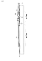
図1は、本発明の第1の実施形態に係るMEMSデバイスを示す平面図である。図2は、図1に示したMEMSデバイスのII−II線に沿った断面図である。なお、平面図において、後述するキャップ部27の内部の構成は、発明の理解を容易にするために、実線で示している。
第2の実施形態は、アクチュエータ25を用いてスイッチを構成したものである。図3は、本発明の第2の実施形態に係るMEMSデバイスを示す平面図である。図4は、図3に示したMEMSデバイスのIV−IV線に沿った断面図である。
第3の実施形態は、アクチュエータ25を用いてLCタンク回路(LC直列共振回路)を構成したものである。図5は、本発明の第3の実施形態に係るMEMSデバイスを示す平面図である。図6は、図5に示したMEMSデバイスのVI−VI線に沿った断面図である。なお、キャップ部27以外の構成は、第1の実施形態と同じである。よって、図5の平面図において、アクチュエータ25及び第1の電極層17の図示は省略する。
以下に、例えばMOSトランジスタ及びMEMSデバイスを備えた半導体装置の製造方法の第1の例について説明する。
以下に、例えばMOSトランジスタ及びMEMSデバイスを備えた半導体装置の製造方法の第2の例について説明する。
以下に、例えばMOSトランジスタ及びMEMSデバイスを備えた半導体装置の製造方法の第3の例について説明する。
以下に、例えばMOSトランジスタ及びMEMSデバイスを備えた半導体装置の製造方法の第4の例について説明する。
以下に、例えばMOSトランジスタ及びMEMSデバイスを備えた半導体装置の製造方法の第5の例について説明する。
Claims (5)
- 半導体基板と、
前記半導体基板の上方に設けられ、かつ上方向に動くアクチュエータと、
前記アクチュエータにより駆動される第1の電極層と、
前記第1の電極層の上方に設けられ、かつ第2の電極層を含むキャップ部と
を具備することを特徴とする半導体装置。 - 前記半導体基板上に設けられ、かつ前記アクチュエータ及び前記第1の電極層を支持する第1の絶縁層と、
前記アクチュエータ上に設けられ、かつ前記第1の絶縁層の膜厚より薄い第2の絶縁層と
をさらに具備し、
前記アクチュエータは、下部電極層と、前記下部電極層の上に設けられた圧電層と、前記圧電層の上に設けられた上部電極層とを含むことを特徴とする請求項1記載の半導体装置。 - 前記第2の電極層は、前記アクチュエータ及び前記第1の電極層を覆い、
前記キャップ部は、前記第2の電極層を支持しかつ前記アクチュエータ及び前記第1の電極層を囲む支持層を含むことを特徴とする請求項1又は2記載の半導体装置。 - 前記キャップ部は、前記第2の電極層の下に設けられた第3の絶縁層を含み、
前記第1の電極層、前記第2の電極層及び前記第3の絶縁層は、可変容量として機能することを特徴とする請求項1乃至3のいずれかに記載の半導体装置。 - 前記第1の電極層及び前記第2の電極層は、スイッチとして機能することを特徴とする請求項1乃至3のいずれかに記載の半導体装置。
Priority Applications (3)
| Application Number | Priority Date | Filing Date | Title |
|---|---|---|---|
| JP2005186854A JP4799059B2 (ja) | 2005-06-27 | 2005-06-27 | 半導体装置 |
| US11/252,882 US7402907B2 (en) | 2005-06-27 | 2005-10-19 | Semiconductor device and manufacturing method thereof |
| CN2006100941354A CN1893137B (zh) | 2005-06-27 | 2006-06-27 | 半导体器件及其制造方法 |
Applications Claiming Priority (1)
| Application Number | Priority Date | Filing Date | Title |
|---|---|---|---|
| JP2005186854A JP4799059B2 (ja) | 2005-06-27 | 2005-06-27 | 半導体装置 |
Publications (2)
| Publication Number | Publication Date |
|---|---|
| JP2007000994A true JP2007000994A (ja) | 2007-01-11 |
| JP4799059B2 JP4799059B2 (ja) | 2011-10-19 |
Family
ID=37568015
Family Applications (1)
| Application Number | Title | Priority Date | Filing Date |
|---|---|---|---|
| JP2005186854A Expired - Fee Related JP4799059B2 (ja) | 2005-06-27 | 2005-06-27 | 半導体装置 |
Country Status (3)
| Country | Link |
|---|---|
| US (1) | US7402907B2 (ja) |
| JP (1) | JP4799059B2 (ja) |
| CN (1) | CN1893137B (ja) |
Cited By (14)
| Publication number | Priority date | Publication date | Assignee | Title |
|---|---|---|---|---|
| KR100808845B1 (ko) * | 2000-05-03 | 2008-03-03 | 컴퓨터 프로세스 컨트롤스 인코포레이티드 | 냉장 시스템 제어 방법 |
| KR100831724B1 (ko) * | 2007-03-12 | 2008-05-22 | 송성현 | 차량용 전원 차단 장치 |
| KR100832627B1 (ko) * | 2006-05-17 | 2008-05-27 | 삼성전기주식회사 | 소결 베어링 모터 |
| KR100841803B1 (ko) * | 2006-09-21 | 2008-06-26 | 김채곤 | 증기를 이용한 보일러장치 |
| JP2008183658A (ja) * | 2007-01-30 | 2008-08-14 | Taiyo Yuden Co Ltd | マイクロカンチレバー |
| JP2008229833A (ja) * | 2007-02-22 | 2008-10-02 | Denso Corp | 半導体装置およびその製造方法 |
| JP2009279733A (ja) * | 2008-05-26 | 2009-12-03 | Toshiba Corp | 微小電気機械システム装置およびその製造方法 |
| JP2010154509A (ja) * | 2008-11-20 | 2010-07-08 | Fujitsu Ltd | 発振器および半導体装置 |
| JP2011506106A (ja) * | 2007-12-07 | 2011-03-03 | エプコス アクチエンゲゼルシャフト | Memsパッケージおよび該memsパッケージの製造方法 |
| JP2011103327A (ja) * | 2009-11-10 | 2011-05-26 | Seiko Epson Corp | 圧電素子、圧電アクチュエーター、液体噴射ヘッドおよび液体噴射装置 |
| US8410561B2 (en) | 2006-11-08 | 2013-04-02 | Seiko Epson Corporation | Electronic device and method for manufacturing thereof |
| US8648663B2 (en) | 2011-04-13 | 2014-02-11 | Seiko Epson Corporation | Oscillator having a plurality of switchable MEMS vibrators |
| US8669824B2 (en) | 2011-03-17 | 2014-03-11 | Seiko Epson Corporation | Oscillator having a plurality of switchable MEMS vibrators |
| JP2014517256A (ja) * | 2011-03-15 | 2014-07-17 | クゥアルコム・メムス・テクノロジーズ・インコーポレイテッド | 金属プルーフマスと圧電部品とを含むマイクロ電気機械システムデバイス |
Families Citing this family (9)
| Publication number | Priority date | Publication date | Assignee | Title |
|---|---|---|---|---|
| US7541209B2 (en) * | 2005-10-14 | 2009-06-02 | Hewlett-Packard Development Company, L.P. | Method of forming a device package having edge interconnect pad |
| US7679186B2 (en) * | 2005-12-08 | 2010-03-16 | Electronics And Telecommunications Research Institute | Piezolectric micro electro-mechanical system switch, array of the switches, and method of fabricating the same |
| JP5232378B2 (ja) * | 2006-10-31 | 2013-07-10 | 株式会社アドバンテスト | 可変容量素子、共振器および変調器 |
| US20080211042A1 (en) * | 2007-02-28 | 2008-09-04 | Seiko Epson Corporation | Method for manufacturing semiconductor device, and semiconductor device |
| US8193685B2 (en) * | 2007-07-03 | 2012-06-05 | Koninklijke Philips Electronics N.V. | Thin film detector for presence detection |
| US8535966B2 (en) | 2010-07-27 | 2013-09-17 | International Business Machines Corporation | Horizontal coplanar switches and methods of manufacture |
| JP5394435B2 (ja) * | 2011-05-13 | 2014-01-22 | 株式会社アドバンテスト | 製造方法、スイッチ装置、伝送路切り替え装置、および試験装置 |
| US20180294409A1 (en) * | 2015-10-07 | 2018-10-11 | William Marsh Rice University | Direct formation porous materials for electronic devices |
| CN113810005A (zh) * | 2021-09-08 | 2021-12-17 | 常州承芯半导体有限公司 | 体声波谐振装置、滤波装置及射频前端装置 |
Citations (4)
| Publication number | Priority date | Publication date | Assignee | Title |
|---|---|---|---|---|
| WO2002088017A1 (en) * | 2001-04-26 | 2002-11-07 | Advantest Corporation | Connection member, microswitch, method for manufacturing connection member, and method for manufacturing microwitch |
| JP2003178663A (ja) * | 1996-08-27 | 2003-06-27 | Omron Corp | マトリックスリレー |
| JP2004287215A (ja) * | 2003-03-24 | 2004-10-14 | Fuji Photo Film Co Ltd | 透過型光変調装置及びその実装方法 |
| JP2004358603A (ja) * | 2003-06-04 | 2004-12-24 | Shinko Electric Ind Co Ltd | マイクロデバイスの製造方法 |
Family Cites Families (12)
| Publication number | Priority date | Publication date | Assignee | Title |
|---|---|---|---|---|
| US33568A (en) * | 1861-10-29 | Improvement in plows | ||
| USRE33568E (en) | 1984-12-21 | 1991-04-09 | General Electric Company | Piezoelectric ceramic switching devices and systems and methods of making the same |
| US4678957A (en) | 1986-06-24 | 1987-07-07 | General Electric Company | Piezoelectric ceramic switching devices and systems and methods of making the same |
| US4675960A (en) * | 1985-12-30 | 1987-06-30 | Motorola, Inc. | Method of manufacturing an electrically variable piezoelectric hybrid capacitor |
| US6359374B1 (en) | 1999-11-23 | 2002-03-19 | Mcnc | Miniature electrical relays using a piezoelectric thin film as an actuating element |
| US6377438B1 (en) | 2000-10-23 | 2002-04-23 | Mcnc | Hybrid microelectromechanical system tunable capacitor and associated fabrication methods |
| TW469657B (en) * | 2000-11-30 | 2001-12-21 | Ind Tech Res Inst | Piezoelectric-actuated adjustable electronic device |
| DE10065013B4 (de) * | 2000-12-23 | 2009-12-24 | Robert Bosch Gmbh | Verfahren zum Herstellen eines mikromechanischen Bauelements |
| WO2003061024A1 (en) * | 2002-01-15 | 2003-07-24 | Matsushita Electric Industrial Co.,Ltd. | Piezoelectric actuator, ink-jet head, and ink-jet recorder |
| US6577476B1 (en) * | 2002-03-28 | 2003-06-10 | International Business Machines Corporation | Flux guide structure for a spin valve transistor which includes a slider body semiconductor layer |
| US7052117B2 (en) * | 2002-07-03 | 2006-05-30 | Dimatix, Inc. | Printhead having a thin pre-fired piezoelectric layer |
| JP4747604B2 (ja) * | 2005-02-18 | 2011-08-17 | Tdk株式会社 | セラミック電子部品 |
-
2005
- 2005-06-27 JP JP2005186854A patent/JP4799059B2/ja not_active Expired - Fee Related
- 2005-10-19 US US11/252,882 patent/US7402907B2/en not_active Expired - Fee Related
-
2006
- 2006-06-27 CN CN2006100941354A patent/CN1893137B/zh not_active Expired - Fee Related
Patent Citations (4)
| Publication number | Priority date | Publication date | Assignee | Title |
|---|---|---|---|---|
| JP2003178663A (ja) * | 1996-08-27 | 2003-06-27 | Omron Corp | マトリックスリレー |
| WO2002088017A1 (en) * | 2001-04-26 | 2002-11-07 | Advantest Corporation | Connection member, microswitch, method for manufacturing connection member, and method for manufacturing microwitch |
| JP2004287215A (ja) * | 2003-03-24 | 2004-10-14 | Fuji Photo Film Co Ltd | 透過型光変調装置及びその実装方法 |
| JP2004358603A (ja) * | 2003-06-04 | 2004-12-24 | Shinko Electric Ind Co Ltd | マイクロデバイスの製造方法 |
Cited By (18)
| Publication number | Priority date | Publication date | Assignee | Title |
|---|---|---|---|---|
| KR100808845B1 (ko) * | 2000-05-03 | 2008-03-03 | 컴퓨터 프로세스 컨트롤스 인코포레이티드 | 냉장 시스템 제어 방법 |
| KR100832627B1 (ko) * | 2006-05-17 | 2008-05-27 | 삼성전기주식회사 | 소결 베어링 모터 |
| KR100841803B1 (ko) * | 2006-09-21 | 2008-06-26 | 김채곤 | 증기를 이용한 보일러장치 |
| US8410561B2 (en) | 2006-11-08 | 2013-04-02 | Seiko Epson Corporation | Electronic device and method for manufacturing thereof |
| JP2008183658A (ja) * | 2007-01-30 | 2008-08-14 | Taiyo Yuden Co Ltd | マイクロカンチレバー |
| JP2008229833A (ja) * | 2007-02-22 | 2008-10-02 | Denso Corp | 半導体装置およびその製造方法 |
| KR100831724B1 (ko) * | 2007-03-12 | 2008-05-22 | 송성현 | 차량용 전원 차단 장치 |
| JP2011506106A (ja) * | 2007-12-07 | 2011-03-03 | エプコス アクチエンゲゼルシャフト | Memsパッケージおよび該memsパッケージの製造方法 |
| US8674498B2 (en) | 2007-12-07 | 2014-03-18 | Epcos Ag | MEMS package and method for the production thereof |
| JP2009279733A (ja) * | 2008-05-26 | 2009-12-03 | Toshiba Corp | 微小電気機械システム装置およびその製造方法 |
| US8581355B2 (en) | 2008-05-26 | 2013-11-12 | Kabushiki Kaisha Toshiba | Micro electric mechanical system device and method of producing the same |
| JP2010154509A (ja) * | 2008-11-20 | 2010-07-08 | Fujitsu Ltd | 発振器および半導体装置 |
| JP2011103327A (ja) * | 2009-11-10 | 2011-05-26 | Seiko Epson Corp | 圧電素子、圧電アクチュエーター、液体噴射ヘッドおよび液体噴射装置 |
| JP2014517256A (ja) * | 2011-03-15 | 2014-07-17 | クゥアルコム・メムス・テクノロジーズ・インコーポレイテッド | 金属プルーフマスと圧電部品とを含むマイクロ電気機械システムデバイス |
| US9000656B2 (en) | 2011-03-15 | 2015-04-07 | Qualcomm Mems Technologies, Inc. | Microelectromechanical system device including a metal proof mass and a piezoelectric component |
| JP2016138890A (ja) * | 2011-03-15 | 2016-08-04 | クゥアルコム・メムス・テクノロジーズ・インコーポレイテッドQUALCOMM MEMS Technologies, Inc. | 金属プルーフマスと圧電部品とを含むマイクロ電気機械システムデバイス |
| US8669824B2 (en) | 2011-03-17 | 2014-03-11 | Seiko Epson Corporation | Oscillator having a plurality of switchable MEMS vibrators |
| US8648663B2 (en) | 2011-04-13 | 2014-02-11 | Seiko Epson Corporation | Oscillator having a plurality of switchable MEMS vibrators |
Also Published As
| Publication number | Publication date |
|---|---|
| US20060292729A1 (en) | 2006-12-28 |
| CN1893137A (zh) | 2007-01-10 |
| CN1893137B (zh) | 2010-12-08 |
| JP4799059B2 (ja) | 2011-10-19 |
| US7402907B2 (en) | 2008-07-22 |
Similar Documents
| Publication | Publication Date | Title |
|---|---|---|
| JP4799059B2 (ja) | 半導体装置 | |
| US7582940B2 (en) | Semiconductor device using MEMS technology | |
| US9617141B2 (en) | MEMS device and process for RF and low resistance applications | |
| US8476804B2 (en) | Piezoelectric MEMS element, voltage control oscillator, communication apparatus, and method of manufacturing piezoelectric drive type MEMS element | |
| CN100477313C (zh) | 可调电容器 | |
| KR101092536B1 (ko) | 압전형 rf 멤스 소자 및 그 제조방법 | |
| US7655995B2 (en) | Semiconductor device using MEMS technology | |
| WO2008052762A2 (de) | Halbleiteranordnung und verfahren zur herstellung einer halbleiteranordnung | |
| US20090051251A1 (en) | Piezoelectric driven mems apparatus and portable terminal | |
| TWI654781B (zh) | 壓電式層裝置的製造方法以及相關的壓電式層裝置 | |
| CN113603053A (zh) | 微机电系统装置 | |
| US7479726B2 (en) | MEMS device using an actuator | |
| TWI496176B (zh) | 微機電系統裝置和製造微機電系統裝置的方法 | |
| JP4713990B2 (ja) | 半導体装置とその製造方法 | |
| WO2007027169A2 (en) | Method of manufacturing silicon topological capacitors | |
| JP4635023B2 (ja) | Mems | |
| JP4857718B2 (ja) | マイクロマシン混載の電子回路装置、およびマイクロマシン混載の電子回路装置の製造方法 | |
| US20250275478A1 (en) | Device structure and manufacturing method thereof | |
| KR100420098B1 (ko) | 초소형 전기기계 시스템을 이용한 고주파 소자 및 그 제조방법 | |
| JP2009078315A (ja) | 封止構造及びその製造方法 | |
| CN119299942A (zh) | 互补性氧化金属半导体声压感测器之制作方法 | |
| TWI516436B (zh) | 微機電系統(mems)裝置及其製造方法 | |
| JP2008149405A (ja) | Memsデバイスの製造方法 | |
| JP2008149394A (ja) | Memsデバイスの製造方法 | |
| JP2017164839A (ja) | 電子装置及び電子装置の製造方法 |
Legal Events
| Date | Code | Title | Description |
|---|---|---|---|
| A621 | Written request for application examination |
Free format text: JAPANESE INTERMEDIATE CODE: A621 Effective date: 20080527 |
|
| A977 | Report on retrieval |
Free format text: JAPANESE INTERMEDIATE CODE: A971007 Effective date: 20101022 |
|
| A131 | Notification of reasons for refusal |
Free format text: JAPANESE INTERMEDIATE CODE: A131 Effective date: 20101026 |
|
| A521 | Request for written amendment filed |
Free format text: JAPANESE INTERMEDIATE CODE: A523 Effective date: 20101224 |
|
| TRDD | Decision of grant or rejection written | ||
| A01 | Written decision to grant a patent or to grant a registration (utility model) |
Free format text: JAPANESE INTERMEDIATE CODE: A01 Effective date: 20110705 |
|
| A01 | Written decision to grant a patent or to grant a registration (utility model) |
Free format text: JAPANESE INTERMEDIATE CODE: A01 |
|
| A61 | First payment of annual fees (during grant procedure) |
Free format text: JAPANESE INTERMEDIATE CODE: A61 Effective date: 20110802 |
|
| FPAY | Renewal fee payment (event date is renewal date of database) |
Free format text: PAYMENT UNTIL: 20140812 Year of fee payment: 3 |
|
| R151 | Written notification of patent or utility model registration |
Ref document number: 4799059 Country of ref document: JP Free format text: JAPANESE INTERMEDIATE CODE: R151 |
|
| FPAY | Renewal fee payment (event date is renewal date of database) |
Free format text: PAYMENT UNTIL: 20140812 Year of fee payment: 3 |
|
| LAPS | Cancellation because of no payment of annual fees |