JP2006514349A - Method and apparatus for determining processor state without interfering with processor operation - Google Patents
Method and apparatus for determining processor state without interfering with processor operation Download PDFInfo
- Publication number
- JP2006514349A JP2006514349A JP2004521558A JP2004521558A JP2006514349A JP 2006514349 A JP2006514349 A JP 2006514349A JP 2004521558 A JP2004521558 A JP 2004521558A JP 2004521558 A JP2004521558 A JP 2004521558A JP 2006514349 A JP2006514349 A JP 2006514349A
- Authority
- JP
- Japan
- Prior art keywords
- processor
- register
- host processor
- data
- instruction
- Prior art date
- Legal status (The legal status is an assumption and is not a legal conclusion. Google has not performed a legal analysis and makes no representation as to the accuracy of the status listed.)
- Withdrawn
Links
Images


Classifications
-
- G—PHYSICS
- G06—COMPUTING OR CALCULATING; COUNTING
- G06F—ELECTRIC DIGITAL DATA PROCESSING
- G06F11/00—Error detection; Error correction; Monitoring
- G06F11/22—Detection or location of defective computer hardware by testing during standby operation or during idle time, e.g. start-up testing
- G06F11/2205—Detection or location of defective computer hardware by testing during standby operation or during idle time, e.g. start-up testing using arrangements specific to the hardware being tested
- G06F11/2236—Detection or location of defective computer hardware by testing during standby operation or during idle time, e.g. start-up testing using arrangements specific to the hardware being tested to test CPU or processors
Landscapes
- Engineering & Computer Science (AREA)
- General Engineering & Computer Science (AREA)
- Theoretical Computer Science (AREA)
- Computer Hardware Design (AREA)
- Quality & Reliability (AREA)
- Physics & Mathematics (AREA)
- General Physics & Mathematics (AREA)
- Advance Control (AREA)
- Test And Diagnosis Of Digital Computers (AREA)
- Multi Processors (AREA)
Abstract
ホストプロセッサの内部状態を判断するための方法及び装置である。テストデータはサービスプロセッサ140の出力ポート152にロードされる。サービスプロセッサ140はホストプロセッサ10に記録される有効ビットをポーリングする。有効ビットはクリアな状態であるとの判断後、サービスプロセッサ140はテストデータをホストプロセッサに送信し、且つ有効ビットをセットする。ステートデータはテストデータに応答して生成される。ステートデータはホストプロセッサ10の出力ポート104に書き込まれる。サービスプロセッサ140はホストプロセッサ10の出力ポート104からデータを受信する。ホストプロセッサ10の状態を判断する演算はホストプロセッサ10の命令の実行を妨げることなく実行される。A method and apparatus for determining the internal state of a host processor. Test data is loaded into the output port 152 of the service processor 140. The service processor 140 polls the valid bit recorded in the host processor 10. After determining that the valid bit is clear, the service processor 140 sends test data to the host processor and sets the valid bit. State data is generated in response to the test data. The state data is written to the output port 104 of the host processor 10. The service processor 140 receives data from the output port 104 of the host processor 10. The operation for determining the state of the host processor 10 is executed without hindering the execution of instructions of the host processor 10.
Description
本発明はプロセッサに関し、さらに具体的にはプロセッサの状態を判断するための方法及び装置に関するものである。 The present invention relates to processors, and more particularly to a method and apparatus for determining the state of a processor.
新しいコンピュータシステム及びシステムソフトウエアの設計時には様々な技術が用いられ、システムプロセッサにより命令が実行される間に様々なハードウエア機構がどのように動くか測定される。システムハードウエアの動作の測定形態の一つとして、プログラムを実行する様々な段階においてプロセッサの状態を判断することが挙げられる。プロセッサの状態を判断することとしてはプロセッサにデータを送ることによりプロセッサを照会することが挙げられる。プロセッサより受信されるデータには処理がなされ、またプロセッサの状態を示す追加データを生成する。そのようなデータには、レジスタやリザベーションステーションなどのコンテンツが含まれる。次いでこの追加データは観察のためにプロセッサから送信される。これに代えて、プロセッサはが部ソースへデータを定期的に送信するように構成されてもよく、データはプロセッサの状態あるいはその他の情報を判断するために用いられる。 Various techniques are used when designing new computer systems and system software to measure how various hardware mechanisms work while instructions are executed by the system processor. One form of measurement of system hardware operation is to determine the state of the processor at various stages of program execution. Determining the state of a processor includes querying the processor by sending data to the processor. Data received from the processor is processed, and additional data indicating the state of the processor is generated. Such data includes content such as registers and reservation stations. This additional data is then transmitted from the processor for observation. Alternatively, the processor may be configured to periodically send data to the department source, where the data is used to determine the status of the processor or other information.
プロセッサにクエリーを送り、プロセッサの状態を判断するために様々なツールが開発されている。これらのツールはテストデータがプロセッサに入力されること、ステートデータがテストデータを受信するプロセッサに応答して生成されること、ステートデータが観察のためにプロセッサから送信されることをそれぞれ許容する。そのようなツールでの1つの難点として、プロセッサを照会する間の命令の実行が挙げられる。典型的には、そのようなツールは、プロセッサの演算がプロセッサクエリの間に割り込みすなわちインタラプトの発生を要求する。プロセッサにより実行される命令ストリームはテストデータを入力するため、ステートデータを生成するため、及びステートデータを出力するために割り込みが必要となる。テストデータを入力すること及びステートデータを出力することは既存の入力及び出力ポートの使用を要求し、その結果プロセッサへの、あるいはプロセッサからのその他のデータの入力及び出力に割り込みが生じる。更に、テストデータの入力はプロセッサが別のサービスルーティンへ切り替える結果をもたらし、このことは現在実行されている命令ストリームを保留する結果をもたらす。これらの要因は特定のルーティンがプロセッサで実行する速度を確定することを困難にする。更に、別のサービスルーティンへの送信はプロセッサクエリから真のプロセッサの状態を判断できなくする結果をもたらす。 Various tools have been developed to query the processor and determine the state of the processor. These tools allow test data to be input to the processor, state data can be generated in response to the processor receiving the test data, and state data can be transmitted from the processor for observation. One difficulty with such tools is the execution of instructions while querying the processor. Typically, such tools require processor operations to generate interrupts or interrupts during processor queries. An instruction stream executed by the processor requires interrupts to input test data, generate state data, and output state data. Inputting test data and outputting state data requires the use of existing input and output ports, which results in interruptions in the input and output of other data to or from the processor. Furthermore, the input of test data results in the processor switching to another service routine, which results in deferring the currently executing instruction stream. These factors make it difficult to determine the speed at which a particular routine executes on the processor. Furthermore, transmission to another service routine results in the inability to determine the true processor state from the processor query.
ホストプロセッサの状態を判断するための方法及び装置が開示されている。一実施例では、サービスプロセッサは、ホストプロセッサのレシーバのレジスタに記録される有効ビットをポーリングする。有効ビットがクリアな状態であると判断されると、サービスプロセッサは出力レジスタにテストデータをロードし、ホストプロセッサへテストデータを送信し、送信が完了すると有効ビットをセットする。有効ビットがセットされたとホストプロセッサで判断されたことに応答して、レシーバのレジスタからテストデータが読み出される。テストデータに応答してホストプロセッサの状態を表すステートデータが生成される。ホストプロセッサは、その出力ポートのトランスミッタのレジスタの有効ビットをポーリングでき、また有効ビットはクリアな状態であるとの検出に応答してトランスミッタのレジスタにデータを保存する。次いでデータはサービスプロセッサのレシーバへ送信され、また有効ビットは既述の送信に応答してセットされる。ホストプロセッサへのデータ送信およびホストプロセッサからのデータ読み出しの演算は命令の実行を割り込むことなく実施される。更に、ホストプロセッサによるデータの送信及び受信はそれぞれ独立して発生する。 A method and apparatus for determining the status of a host processor is disclosed. In one embodiment, the service processor polls for valid bits recorded in the register of the host processor's receiver. If it is determined that the valid bit is clear, the service processor loads the test data into the output register, transmits the test data to the host processor, and sets the valid bit when the transmission is complete. In response to the host processor determining that the valid bit has been set, test data is read from the register of the receiver. State data representing the state of the host processor is generated in response to the test data. The host processor can poll the valid bit of the transmitter's register for its output port and saves data in the transmitter's register in response to detecting that the valid bit is clear. The data is then transmitted to the service processor receiver, and the valid bit is set in response to the previously described transmission. The operations of data transmission to the host processor and data reading from the host processor are performed without interrupting execution of instructions. Furthermore, transmission and reception of data by the host processor occur independently of each other.
一実施例では、ホストプロセッサは入力ポート及び出力ポートを備えている。ホストプロセッサの入力ポートはサービスプロセッサの出力ポートと結合されるために構成される。一方で出力ポートはサービスプロセッサの入力ポートと結合されるために構成される。両ホスト及びサービスプロセッサの入力ポート及び出力ポートはそれぞれ多くのビットを記録するように構成されるレジスタを含む。各レジスタはセットされる際に記録されるデータは有効であることを表す有効ビットを記録するように構成される。入力ポートのレジスタは有効ビットがクリアな状態であるときにだけデータを受信するように構成される。データが出力ポートから入力ポートへ送信される際に、有効ビットは入力ポートのレジスタにセットされる。両ホストプロセッサ及びサービスプロセッサは、有効ビットがセットされるとの検出に応答してそれぞれの入力ポートのレジスタから読み出されるように構成される。 In one embodiment, the host processor has an input port and an output port. The host processor input port is configured to be coupled to the service processor output port. On the other hand, the output port is configured to be coupled with the input port of the service processor. Both the host and service processor input and output ports each include a register configured to record a number of bits. Each register is configured to record a valid bit indicating that the data recorded when set is valid. The input port register is configured to receive data only when the valid bit is clear. When data is transmitted from the output port to the input port, the valid bit is set in the input port register. Both host processors and service processors are configured to be read from the registers of their respective input ports in response to detecting that the valid bit is set.
サービスプロセッサの一実施例ではデータは出力ポートのレジスタにロードされ、あるいはIEEE1149.1規格と一致する境界走査試験アクセスポート(バウンダリースキャンテストアクセスポート)(TAP)を通って入力ポートから読み出される。データはテストデータ入力(TDI)ピンを通ってサービスプロセッサの出力ポートのレジスタへ順次ロードされる。同様にデータはテストデータ出力(TDO)ピンを通ってサービスプロセッサの出力ポートのレジスタから順次シフトされる。 In one embodiment of the service processor, data is loaded into an output port register or read from an input port through a boundary scan test access port (Boundary Scan Test Access Port) (TAP) consistent with the IEEE 1149.1 standard. Data is loaded sequentially through the test data input (TDI) pin into the service processor output port registers. Similarly, data is sequentially shifted from the service processor output port registers through the test data output (TDO) pin.
多くの実施例では、入力ポート及び出力ポートを組み合わせたオペレーションは、互いに別々に動作する。つまりサービスプロセッサの出力ポートは、ホストプロセッサの出力ポートからサービスプロセッサの入力ポートへのいずれのデータ送信からも独立してホストプロセッサの入力ポートへデータを送信する。更に異なる実施例ではデータはプロセッサへあるいはプロセッサから定期的に送信され、あるいはデータは個々の照会に応答してプロセッサから送信される。 In many embodiments, operations that combine input ports and output ports operate separately from each other. That is, the service processor output port transmits data to the host processor input port independently of any data transmission from the host processor output port to the service processor input port. In yet another embodiment, data is sent periodically to or from the processor, or data is sent from the processor in response to individual queries.
本発明は、様々な改良を行い、また、他の形態で実施することができるが、ここに説明されている特定の実施例は、例示として示さたものであり、以下にその詳細を記載する。しかし当然のことながら、ここに示した特定の実施例は、本発明を開示されている特定の形態に限定するものではなく、むしろ本発明は添付の請求項によって規定されている発明の範疇に属する全ての改良、等価物、及び変形例をカバーするものである。 While the invention is amenable to various modifications and alternative forms, specific embodiments described herein have been shown by way of example and are described in detail below. . It should be understood, however, that the particular embodiments shown are not intended to limit the invention to the particular form disclosed, but rather to fall within the scope of the invention as defined by the appended claims. Covers all improvements, equivalents, and variations to which it belongs.
図1に、プロセッサ10の一実施例のブロック図が示されている。別の実施例も可能であり、検討される。図1に示されているように、プロセッサ10はプリフェッチ/プレデコードユニット12、分岐予測ユニット14、命令キャッシュ16、命令整合ユニット18、複数のデコードユニット20A−20C、複数のリザベーションステーション22A−22C、複数のファンクショナルユニット24A−24C、ロード/ストアユニット26、データキャッシュ28、レジスタファイル30、リオーダーバッファ32、MROMユニット34、及びバスインターフェースユニット37を含む。文字の後に続く特定の参照番号を備えた、本明細書に参照される要素は単独の参照番号により集合的に参照される。例えばデコードユニット20A−20Cは集合的にデコードユニット20として参照される。
A block diagram of one embodiment of the
プリフェッチ/プレデコードユニット12は、バスインターフェースユニット37から命令を受信するために結合されている。また更にプリフェッチ/プレデコードユニット12は命令キャッシュ16及び分岐予測ユニット14と結合される。同様に、分岐予測ユニット14は命令キャッシュ16と結合される。また更に分岐予測ユニット14はデコードユニット20及びファンクショナルユニット24と結合される。命令キャッシュ16は、更に、MROMユニット34及び命令整合ユニット18と結合される。命令整合ユニット18は順にデコードユニット20と結合される。各デコードユニット20A−20Cはロード/ストアユニット26と、及びそれぞれのリザベーションステーション22A−22Cと結合される。リザベーションステーション22A−22Cは更にそれぞれのファンクショナルユニット24A−24Cと結合される。加えてデコードユニット20及びリザベーションステーション22はレジスタファイル30及びリオーダーバッファ32と結合される。ファンクショナルユニット24もまたロード/ストアユニット26、レジスタファイル30、及びリオーダーバッファ32と結合される。データキャッシュ28はロード/ストアユニット26と、及びバスインターフェースユニット37と結合される。バスインターフェースユニット37は更にL2キャッシュへのL2インターフェースとバスとに結合される。最後にMROMユニット34はデコードユニット20と結合される。
Prefetch / predecode unit 12 is coupled to receive instructions from bus interface unit 37. Still further, the prefetch / predecode unit 12 is coupled to the
命令キャッシュ16は高速キャッシュメモリであり、命令を記録するために提供される。命令は命令キャッシュ16から取り出されつまりフェッチされ、デコードユニット20へ送られる。一実施例では命令キャッシュ16は64バイトライン(1バイトは8バイナリバイトより成る)を有する2ウエイセットアソシエイティブ構造の64キロバイトを上限とする命令を記録するように構成される。あるいはその他いずれの所望の構造及びサイズが用いられてよい。例えば、命令キャッシュ16はフルアソシエイティブ、セットアソシエイティブ、あるいはダイレクトマップ構造として実施されてよいことに留意されたい。
The
命令はプリフェッチ/プレデコードユニット12により命令キャッシュ16に記録される。命令はプリフェッチスキームにより、命令キャッシュ16からその要求前にプリフェッチされる。プリフェッチ/プレデコードユニット12により様々なプリフェッチスキームが用いられる。プリフェッチ/プレデコードユニット12は命令キャッシュ16に命令を送信するので、プリフェッチ/プレデコードユニット12は命令に対応するプレデコードデータを生成する。例えば一実施例では、プリフェッチ/プレデコードユニット12は命令の各バイトに対し3つのプレデコードビットを生成する。それらはスタートビット、エンドビット、及びファンクショナルビットである。プレデコードビットは各命令の境界を示すタグを形成する。プレコードタグはまた、所定の命令がデコードユニット20により直接デコードされ得るかどうか、あるいは命令はMROMユニット34により制御されるマイクロコードプロシージャを呼出して実行されるかどうか、などの付加的な情報も送信する。更にまた、プリフェッチ/プレデコードユニット12は分岐命令を検出するように構成され、また分岐命令に対応する分岐予測情報を分岐予測ユニット14に記録するように構成される。その他の実施例は所望に応じていずれの適切なプレデコードスキームを用いてもよく、またプレデコードを用いなくてもよい。
Instructions are recorded in the
可変バイト長の命令セットを用いるプロセッサ10の実施例に対するプレデコードタグの符号化の1つが以下に解説される。可変バイト長の命令セットは異なる命令が異なるバイト数を占める命令セットである。プロセッサ10の一実施例により用いられる典型的な可変バイト長命令セットはx86命令セットである。
One encoding of the predecode tag for an embodiment of the
典型的な符号化では、所定のバイトが命令の第1バイトの場合、そのバイトに対するスタートビットがセットされる。バイトが命令の最後のバイトの場合、そのバイトに対するエンドビットがセットされる。デコードユニット20により直接デコードされる命令は“高速経路”命令として参照される。残りのx86命令は一実施例によればMROM命令として参照される。高速経路命令に対しては、命令に含まれる各プレフィックスバイトに対してファンクショナルビットがセットされ、その他のバイトに対してはクリアな状態にされる。代わりに、MROM命令に対しては、ファンクショナルビットは各プレフィックスバイトに対してクリアな状態にされ、その他のバイトに対してはセットされる。命令の種類はエンドバイトに対応するファンクショナルビットを調べることにより判断される。そのファンクショナルビットがクリアな状態の場合、命令は高速命令である。反対にそのファンクショナルビットがセットされる場合、命令はMROM命令である。命令のオペレーションコードはそれにより命令の第1のクリアファンクショナルビットに関連するバイトとしてデコードユニット20により直接デコードされる命令に配置される。例えば2プレフィックスバイト、ModR/Mバイト、イミディエイトバイト(immediate byte)を含む高速経路命令は以下のようなスタート、エンド、ファンクショナルビットを有する。
スタートビット 10000
エンドビット 00001
ファンクショナルビット 11000
In typical encoding, if a given byte is the first byte of an instruction, the start bit for that byte is set. If the byte is the last byte of the instruction, the end bit for that byte is set. Instructions that are directly decoded by the decode unit 20 are referred to as “fast path” instructions. The remaining x86 instructions are referred to as MROM instructions according to one embodiment. For fast path instructions, the functional bit is set for each prefix byte included in the instruction and cleared for the other bytes. Instead, for MROM instructions, the functional bit is cleared for each prefix byte and set for the other bytes. The type of instruction is determined by examining the functional bit corresponding to the end byte. If the functional bit is clear, the instruction is a high speed instruction. Conversely, if the functional bit is set, the instruction is an MROM instruction. The instruction's operation code is thereby placed in the instruction that is directly decoded by the decode unit 20 as a byte associated with the first clear functional bit of the instruction. For example, a fast path instruction including two prefix bytes, ModR / M byte, immediate byte has the following start, end, and functional bits.
Start bit 10,000
End bit 00001
Functional bit 11000
MROM命令は、デコードユニット20によりデコードするには複雑すぎると判断される命令である。MROM命令はMROMユニット34を呼出すことにより実行される。更に具体的には、MROM命令を受けると、MROMユニット34は決められた高速経路命令のサブセットへ命令を解析し発行し、所望の演算を達成する。MROMユニット34はデコードユニット20へ高速経路命令のサブセットを送る。
The MROM instruction is an instruction that is determined to be too complicated to be decoded by the decoding unit 20. The MROM instruction is executed by calling the
プロセッサ10は、分岐予測を用いて条件付分岐命令に続いて投機的に命令をフェッチする。分岐予測ユニット14は分岐予測演算を実行するために含まれる。一実施例では、分岐予測ユニット14は分岐ターゲットバッファを用いる。分岐ターゲットバッファは、命令キャッシュ16に、キャッシュラインの16バイト部ごとに、2つを上限とする分岐ターゲットアドレス及びそれに対応した採用された/採用されなかった予測をキャッシュする。分岐ターゲットバッファは例えば2048のエントリあるいはその他の適切な数のエントリを有す。プリフェッチ/プレコードユニット12は特定の行がプレデコードされる際、初期の分岐ターゲットを判断する。続いてキャッシュラインと対応する分岐ターゲットへのアップデートが、キャッシュラインの命令を実行することにより発生する。命令キャッシュ16は、フェッチされている命令アドレスの指示を与えて、分岐予測ユニット14が分岐予測を形成するためにどの分岐ターゲットアドレスを選択するかを決定できるようにする。デコードユニット20及びファンクショナルユニット24は分岐予測ユニット14へアップデート情報を送る。デコードユニット20は分岐予測ユニット14により予測されなかった分岐命令を検出する。ファンクショナルユニット24は分岐命令を実行し、予測された分岐方向が間違っているかどうかを判断する。分岐方向が“採用され”た場合、続く命令は分岐命令のターゲットアドレスからフェッチされる。反対に、分岐方向は“採用されない”場合、次の命令は分岐命令に続いてメモリ位置からフェッチされる。誤予測分岐命令が検出されると、誤予測分岐に続く命令はプロセッサ10の様々なユニットから破棄される。他の構成として、分岐予測ユニット14はデコードユニット20及びファンクショナルユニット24の代わりにリオーダーバッファ32と結合され、且つ、リオーダーバッファ32から分岐誤予測情報を受信する。様々な適切な分岐予測アルゴリズムは分岐予測ユニット14により用いられる。
The
命令キャッシュ16からフェッチされる命令は、命令整合ユニット18に伝達される。命令は命令キャッシュ16からフェッチされるので、対応するプレデコードデータは走査され、フェッチされる命令に関し命令整合ユニット18(及びMROMユニット34)へ情報が送られる。命令整合ユニット18は走査データを利用し、各デコードユニット20へ命令を整合する。一実施例では、命令整合ユニット18は3セットの8命令バイトからデコードユニット20へ命令を整合する。デコードユニット20Aはデコードユニット20B及び20C(プログラム順序で)により同時に受信される命令よりも前の命令を受信する。同様にデコードユニット20Bはプログラム順序でデコードユニット20Cにより同時に受信される命令よりも前の命令を受信する。いくつかの実施例では(例:固定長の命令セットを用いた実施例)、命令整合ユニット18はなくされる。
Instructions fetched from the
デコードユニット20は命令整合ユニット18から受信される命令をデコードするように構成される。レジスタオペランド情報は検出され、レジスタファイル30及びリオーダーバッファ32へ送られる。加えて、1つ以上のメモリ演算の実施を命令が要求する場合、デコードユニット20は、メモリ演算をロード/ストアユニット26へ送る。各命令はファンクショナルユニット24に対する一連のコントロール値にデコードされ、またこれらのコントロール値は命令に含まれる置換えあるいは即値データとオペランドアドレス情報とともにリザベーションステーション22へ送られる。1つの具体的な実施例では、各命令はファンクショナルユニット24A−24Cにより別々に実施される2つを上限とする演算にデコードされる。
The decode unit 20 is configured to decode instructions received from the instruction matching unit 18. Register operand information is detected and sent to the
プロセッサ10は、アウトオブオーダー実行をサポートする。従ってリオーダーバッファ32を用いてレジスタリード及びライト演算に対しオリジナルプログラムのシーケンスの経過を追い、レジスタリネームを実施し、投機的な命令の実行と分岐誤予測回復を許容し、“正確な”例外(precise exceptions)となるよう促進する。リオーダーバッファ32内の一時的な記録場所はレジスタのアップデートを含む命令をデコード後にリザーブされ、その結果投機的なレジスタの状態を記録する。分岐予測が間違いの場合、誤予測経路に沿った投機的に実行される命令の結果はレジスタファイル30に書き込まれる前にバッフアにて無効にされうる。同様に、特定の命令が例外を引き起こす場合、特定の命令に続く命令は破棄される。このような方法で例外は“正確”である(すなわち、例外を引き起こす特定の命令に続く命令は例外の前には完了されない)。ここで留意すべきは、特定の命令というのはプログラムの順序で特定の命令に先行する命令の前に実行される場合は投機的に実効されることである。先行する命令は分岐命令あるいは例外を引き起こす命令であり、いずれの場合にも投機的な結果はリオーダーバッファ32により破棄される。
The
デコードユニット20の出力において送られるデコードされる命令はそれぞれのリザベーションステーション22へ直接送られる。一実施例では各リザベーションステーション22は対応するファンクショナルユニットへの発行を待つ上限6つの保留命令に対し命令情報(例:オペランド値、オペランドタグ及び/あるいは即値データと同様、デコードされる命令)を保持することができる。ここで留意すべきは、図1の実施例に対して、各リザベーションステーション22は専用のファンクショナルユニットと関連付けられている点である。したがって3つの専用”発行部(issue portion)”、はリザベーションステーション22及びファンクショナルユニット24により形成される。つまり、発行部0はリザベーションステーション22A及びファンクショナルユニット24Aにより形成される。リザベーションステーション22Aへ整合され、また送られる命令はファンクショナルユニット24Aにより実行される。同様に、発行部1はリザベーションステーション22Bとファンクショナルユニット24Bにより形成される。発行部2はリザベーションステーション22Cとファンクショナルユニット24Cにより形成される。
The decoded instruction sent at the output of the decode unit 20 is sent directly to the respective reservation station 22. In one embodiment, each reservation station 22 provides instruction information (eg, decoded instructions as well as operand values, operand tags, and / or immediate data) for up to six pending instructions waiting to be issued to the corresponding functional unit. Can be held. Note that, for the embodiment of FIG. 1, each reservation station 22 is associated with a dedicated functional unit. Thus, three dedicated “issue portions” are formed by the reservation station 22 and the functional unit 24. That is, the issuing unit 0 is formed by the reservation station 22A and the
特定の命令をデコード後、所望のオペランドがレジスタ位置にある場合、レジスタアドレス情報はリオーダーバッファ32とレジスタファイル30へ同時に送られる。レジスタファイル30はプロセッサ10により実施される命令セットに含まれる各々の設計されたレジスタに対し記録場所を有す。追加の記録場所はMROMユニット34により用いられるためにレジスタファイル30に含まれる。リオーダーバッファ32は、これらのレジスタのコンテントを変更する結果に対し一時的な記録場所を有し、その結果アウトオブオーダー実行を許容する。リオーダーバッファ32の一時的な記録場所は各命令に対しリザーブされ、各命令はデコード後に実レジスタの1つのコンテントを修正するために判断される。従って、特定のプログラムを実行する間、様々なポイントでは、リオーダーバッファ32は1つ以上の場所を有し、それらは所定のレジスタの投機的に実施されるコンテントを含む。所定の命令のデコードに続いて、リオーダーバッファ32が前の場所あるいは所定の命令でオペランドとして用いられるレジスタに割振られた場所を有すると判断される場合、リオーダーバッファ32は 1)直前に割振られた場所の値、あるいは2)最終的に前の命令を実行するファンクショナルユニットにより値が生成されていない場合に、直前に割振られた場所に対するタグ、のどちらか一方を対応のリザベーションステーションへフォーワードする。リオーダーバッファ32が所定のレジスタに対しリザーブされる場所を有する場合、オペランド値(あるいはリオーダーバッファタグ)がレジスタファイル30からではなくリオーダーバッファ32から送られる。リオーダーバッファ32にて要求されるレジスタに対しリザーブされる場所を有さない場合、値はレジスタファイル30から直接取られる。オペランドがメモリ位置に対応する場合、オペランド値はロード/ストアユニット26を通ってリザベーションステーションに送られる。
After decoding a particular instruction, if the desired operand is in a register location, register address information is sent to reorder buffer 32 and register
1つの具体的な実施例では、リオーダーバッファ32はユニットとして同時にデコードされる命令を記録し処理するように構成される。この構成は“行型”として本明細書に参照される。いくつもの命令を一緒に処理することにより、リオーダーバッファ32に用いられるハードウエアを単純化することができる。例えば本実施例に含まれる行型のリオーダーバッファは1つ以上の命令がデコードユニット20により送られるときは、いつでも3つの命令(各デコードユニット20から1つ)に関する命令情報に対し十分な記録を割振る。それに対し、可変長の記録は、実際に送られる命令の数に応じて従来のリオーダーバッファに割振られる。相対的に大きな数の論理ゲートが可変長の記録を割振るために必要とされる。同時にデコードされる命令の各々が実行される場合、命令の結果はレジスタファイル30に同時に記録される。次いで記録は別の一連の同時にデコードされる命令へ自由に割振ることができる。加えて命令ごとに用いられる制御論理回路の総数は、制御論理が様々な同時にデコードされる命令上に償却されるため、低減される。特定の命令を識別するデコーダーバッファタグは二つのフィールドに分割される。ラインタグとオフセットタグである。ラインタグは特定の命令を含む一連の同時にデコードされる命令を識別し、またオフセットタグはセットのどの命令が特定の命令と対応するかを識別する。留意すべきは命令を記録することはレジスタファイル30をもたらし、対応の記録を自由にすることは命令を”リタイアする”として参照されることである。更に留意すべきはいずれのリオーダーバッファ構成もプロセッサ10の様々な実施例において用いられることである。
In one specific embodiment, reorder buffer 32 is configured to record and process instructions that are simultaneously decoded as a unit. This configuration is referred to herein as “row type”. By processing several instructions together, the hardware used for the reorder buffer 32 can be simplified. For example, the row-type reorder buffer included in this embodiment provides sufficient recording for instruction information regarding three instructions (one from each decode unit 20) whenever one or more instructions are sent by the decode unit 20. Allocate. On the other hand, variable length records are allocated to the conventional reorder buffer according to the number of instructions actually sent. A relatively large number of logic gates are required to allocate variable length records. If each of the instructions decoded at the same time is executed, the result of the instruction is recorded in the
先に述べたように、リザベーションステーション22は対応のファンクショナルユニット24により命令が実行されるまで命令を記録する。命令は(i)命令のオペランドが提供されている場合;及び(ii)オペランドが同じリザベーションステーション22A−22Cにあるとともにプログラム順序で命令の前にある命令が提供されていない場合、実行するよう選択される。命令がファンクショナルユニット24の1つにより実行される場合、その命令の結果はその結果を待ついずれのリザベーションステーション22へ直接パスされ、同時に結果はリオーダーバッファ32をアップデートするためにパスされる(この技術は、一般にリザルトフォワーディング(result forwarding)と称される)。命令は実行するために選択され、クロックサイクルの間、関連する結果がフォーワードされるファンクショナルユニット24A−24Cへパスされる。リザベーションステーション22はこの場合、フォワードされる結果をファンクショナルユニット24へ送る。命令が、ファンクショナルユニット24により実行される様々な演算にデコードされるという実施例では、演算はそれぞれ別々にスケジュールされる。
As stated above, the reservation station 22 records instructions until the instructions are executed by the corresponding functional unit 24. The instruction is selected to execute if (i) the operand of the instruction is provided; and (ii) if the operand is in the same reservation station 22A-22C and the instruction preceding the instruction in program order is not provided Is done. When an instruction is executed by one of the functional units 24, the result of the instruction is passed directly to any reservation station 22 waiting for the result, while the result is passed to update the reorder buffer 32 ( This technique is commonly referred to as result forwarding). Instructions are selected for execution and passed to
一実施例では、各ファンクショナルユニット24はシフト、送信、論理演算、ブランチ演算と同様に、加算及び引き算の整数算術演算を実施するように構成される。演算はデコードユニット20により特定の命令に対しデコードされるコントロール値に応答して実施される。浮動小数点ユニット(図示せず)もまた用いられ、浮動小数点演算に適応される。浮動小数点ユニットはMROMユニット34あるいはリオーダーバッファ32から命令を受信し、その後リオーダーバッファ32と通信し命令を完了するコプロセッサとして、オペレーションがなされる。加えて、ファンクショナルユニット24はロード/ストアユニット26により実施されるロード及びストアメモリ演算に対しアドレス生成を実施するように構成される。1つの特定の実施例では、各ファンクショナルユニット24はアドレスを生成するためのアドレス生成ユニット及び残りのファンクションを実施するための実行ユニットを有す。2つのユニットはクロックサイクルの間、異なる命令あるいは演算から独立してオペレーションがなされる。
In one embodiment, each functional unit 24 is configured to perform integer arithmetic operations of addition and subtraction, as well as shift, transmission, logical operations, and branch operations. The operation is performed in response to a control value decoded by the decode unit 20 for a specific instruction. A floating point unit (not shown) is also used and adapted for floating point operations. The floating point unit operates as a coprocessor that receives instructions from the
各ファンクショナルユニット24は、また分岐予測ユニット14への条件付分岐命令の実行に関して情報を送る。分岐予測が間違いであった場合、分岐予測ユニット14は命令処理パイプラインに入った誤予測ブランチの後に命令を流し、そして命令キャッシュ16あるいはメインメモリから要求される命令をフェッチさせる。留意すべきはそのような状況において、投機的に実施された、及び一時的にロード/ストアユニット26およびリオーダーバッファ32に記録されるものを含む、誤予測分岐命令の破棄後に発生するオリジナルプログラムシーケンスの命令の結果は破棄されるということである。さらに留意すべきはブランチ実行の結果はファンクショナルユニット24によりリオーダーバッファ32へ送られることであり、それはファンクショナルユニット24への分岐誤予測を表す。
Each functional unit 24 also sends information regarding the execution of conditional branch instructions to the
ファンクショナルユニット24により生成される結果はレジスタ値がアップデートされる場合はリオーダーバッファ32へ送られ、またメモリ位置のコンテントが変更される場合はロード/ストアユニット26へ送られる。結果がレジスタに記録されるものである場合、リオーダーバッファ32は命令がデコードされた際にレジスタの値に対してリザーブされる位置に結果を記録する。複数のリザルトバス38は、ファンクショナルユニット24及びロード/ストアユニット26から結果をフォーワードするために含まれる。リザルトバス38は実行される命令を認識するリオーダーバッファタグと同様、生成される結果を運ぶ。 The result generated by the functional unit 24 is sent to the reorder buffer 32 when the register value is updated, and to the load / store unit 26 when the content of the memory location is changed. If the result is to be recorded in a register, reorder buffer 32 records the result in a location that is reserved for the value of the register when the instruction is decoded. A plurality of result buses 38 are included to forward results from the functional unit 24 and the load / store unit 26. The result bus 38 carries the results generated as well as a reorder buffer tag that recognizes the instruction to be executed.
ロード/ストアユニット26は、ファンクショナルユニット24とデータキャッシュ28との間にインターフェースを提供する。一実施例ではロード/ストアユニット26は第1ロード/ストアバッファと第2ロードストア/バッファを有する。第1ロード/ストアバッファはデータキャッシュ28にアクセスしていない保留のロードあるいはストアに対しデータ及びアドレス情報に対する記録場所を有して構成される。第2ロード/ストアバッファはデータキャッシュ28にアクセスしたロード及びストアに対するデータ及びアドレス情報に対する記録場所を有して構成される。例えば第1バッファは12の場所を有し、第2バッファは32の場所を有する。デコードユニット20はロード/ストアユニット26へのアクセスのために調停する。第1バッファがフルの状態であるとき、デコードユニットは保留のロードあるいはストアの要求情報に対しロード/ストアユニット26が空きを有するまで待たなければならない。ロード/ストアユニット26はまた保留のストアメモリ演算に対してロードメモリ演算のためにディペンデンシーチェックを行い、データの一貫性が維持されていることを確認する。メモリ演算はプロセッサ10とメインメモリサブシステムとの間のデータ送信である(送信はデータキャッシュ28で達成されるが)。メモリ演算はメモリに記録されるオペランドを利用する命令の結果である。あるいはデータの送信を引き起こすがその他の演算は引き起こさないロード/ストア命令の結果である。
The load / store unit 26 provides an interface between the functional unit 24 and the data cache 28. In one embodiment, the load / store unit 26 has a first load / store buffer and a second load store / buffer. The first load / store buffer is configured to have a recording location for data and address information for pending loads or stores not accessing the data cache 28. The second load / store buffer has a recording location for data and address information for loads and stores that have accessed the data cache 28. For example, the first buffer has 12 locations and the second buffer has 32 locations. The decode unit 20 arbitrates for access to the load / store unit 26. When the first buffer is full, the decode unit must wait until the load / store unit 26 is free for pending load or store request information. The load / store unit 26 also performs a dependency check for the load memory operation on the pending store memory operation to confirm that the data consistency is maintained. Memory operations are data transmissions between the
データキャッシュは、ロード/ストアユニット26とメインメモリサブシステムとの間に送信されるデータを一時的に記録するために設けられる高速のキャッシュメモリである。一実施例では、データキャッシュ28は2ウエイセットアソシエイティブ構造で64キロバイトを上限とする記録容量を有する。データキャッシュ28はセットアソシエイティブ構造、フルアソシエイティブ構造、ダイレクトマップ構造、及びその他の適切な構造の適切なサイズを含む様々な具体的なメモリ構造で実施される。 The data cache is a high-speed cache memory provided for temporarily recording data transmitted between the load / store unit 26 and the main memory subsystem. In one embodiment, the data cache 28 has a two-way set associative structure and a recording capacity up to 64 kilobytes. Data cache 28 may be implemented with a variety of specific memory structures including set associative structures, full associative structures, direct map structures, and other suitable structures in appropriate sizes.
バスインターフェースユニット37はプロセッサ10とバスを介するコンピュータシステムのその他のコンポーネントとの間を通信するように構成される。例えばバスはデジタル イクイップメント コーポレーション(Digital Equipment Corporation)により開発されたEV−6バスと互換性がある。その他、パケットベース、単方向あるいは双方向リンクなどを含むいずれの適切な相互接続構造を用いることが出来る。任意のL2キャッシュインターフェースもまたレベル2キャッシュへインターフェース接続のため、同様に用いられる。
The bus interface unit 37 is configured to communicate between the
留意すべきは、図1の実施例はスーパースカラ実行であるが、その他の実施例はスカラ実行を用いてもよいということである。更に、ファンクショナルユニットの数は実施例により異なる。その他の実施例は図1に示されている個々のリザベーションステーションではなくセントラルリザベーションステーションを用いてもよい。更にその他の実施例は図1のリザベーションステーション及びリオーダーバッファではなくセントラルスケジューラを用いる。 Note that although the embodiment of FIG. 1 is superscalar execution, other embodiments may use scalar execution. Furthermore, the number of functional units varies depending on the embodiment. Other embodiments may use a central reservation station rather than the individual reservation stations shown in FIG. Yet another embodiment uses a central scheduler rather than the reservation station and reorder buffer of FIG.
プロセッサ10は、メールボックス100としてここに示されるようにポートを含む。ポートは命令ストリームを実行する間、照会されるのを許容する。メールボックスポート100はプロセッサ10の外側にあるサービスプロセッサあるいはデバッグプロセッサと結合されるために構成される。プロセッサ10の状態を照会するために用いられるテストデータはメールポート100を介して受信される。同様に、照会から生じるプロセッサ10の状態を示すステートデータはメールボックスポート100からサービスプロセッサあるいはデバッグプロセッサへ送信される。メールボックスポート100はデコードユニット20A−20C、レジスタファイル30、命令キャッシュ16、ファンクショナルユニット24A−24Cなど1つ以上のプロセッサ10のユニットと結合される。情報はメールボックスポート100から送信あるいは受信される。
The
図2に、プロセッサの状態を判断するシステムの一実施例のブロック図が示されている。この実施例は、プロセッサ10、以後ホストプロセッサ10はサービスプロセッサ140と結合される。いくつかの実施例では、サービスプロセッサ140はホストプロセッサ10が実施されるコンピュータシステムに結合されるもうひとつのコンピュータシステムに配置される。その他の実施例では、サービスプロセッサ140はホストプロセッサが配置されるコンピュータシステムの周辺スロットに挿入されるボード上に配置される、あるいはホストプロセッサと同じボードに取り付けられる。
FIG. 2 shows a block diagram of one embodiment of a system for determining the state of a processor. In this embodiment,
先に述べたように、ホストプロセッサ10は、メールボックスポート100を含む。メールボックスポート100はメールボックス入力ポート102及びメールボックス出力ポート104を含む。メールボックス入力ポート102はサービスプロセッサ140のコンプリメンタリ出力ポート152と結合するように構成される。同様にメールボックス出力ポート104はサービスプロセッサ140のコンプリメンタリ入力ポート154と結合するように構成される。
As previously mentioned, the
ホストプロセッサ10のメールボックス入力ポート102はサービスプロセッサ140から送信されるテストデータを受信する。テストデータはサービスプロセッサ140の出力ポート152からホストプロセッサ10のメールボックス入力ポート102へ送信される。同様に、サービスプロセッサ140はホストプロセッサ10からステートデータを受信するように構成される。ステートデータはホストプロセッサ10のメールボックス出力ポート104からサービスプロセッサ140の入力ポート154へ送信される。入力/出力ポートの各コンプリメンタリペアは互いに独立して機能する。つまり出力ポート152はメールボックス出力ポート104から入力ポート154へのステートデータのいずれの送信からも独立して、メールボックス入力ポート102へテストデータを送信する。
The
テストデータはサービスプロセッサ140の出力ポート152へ、テストアクセスポート(TAP)の一部であるテストデータ入力(TDI)ピンを介して、連続的にロードされる。テストアクセスポートはIEEE規格1149.1と互換性のある境界走査(バウンダリスキャン)ポートである。同様にステートデータはテストデータ出力ピンを介して入力ポート154から連続的にシフトされる。サービスプロセッサ140からのテストデータのロード及びステートデータのアンロードについての追加の詳細は以下に解説される。
Test data is continuously loaded into the
図3はサービスプロセッサ出力ポートに結合されるホストプロセッサ入力ポートの一実施例を例示したブロック図である。実施例ではホストプロセッサ10のメールボックス入力ポート102はサービスプロセッサ140のメールボックス出力ポート152と結合されている。メールボックス入力ポート102は入力レジスタ112を含む。入力レジスタ112はテストデータを受信及び記録するように構成されている。テストデータは出力ポート152に配置される出力レジスタ162から受信される。両出力レジスタ162及び入力レジスタ112は様々な大きさである。一実施例では、出力レジスタ162及び入力レジスタ112は32ビットのデータと1つの有効ビットを記録するように構成される。多様なレジスタ(両メールボックス入力ポート及び両メールボックス出力ポートに対して)と同様、異なるレジスタサイズを有するその他の実施例も可能であり、検討される。
FIG. 3 is a block diagram illustrating one embodiment of a host processor input port coupled to a service processor output port. In the exemplary embodiment,
ホストプロセッサ10の状態を判断するため、入力レジスタ112の有効ビットは出力レジスタ162へのテストデータのローディングに続いて、照会されなければならない。
先に述べたように、データはIEEE1149.1規格と互換性のある境界走査TAPを介してメールボックス出力ポート152へロードされる。示されている一実施例では、出力レジスタ162はTDIピンと結合される。テストデータは連続的にTDIピンを介して出力レジスタ162にシフトされる。テストデータに加えて、有効ビットもまたTDIピンを介して出力レジスタにセットされる。
To determine the state of the
As previously mentioned, the data is loaded into the
入力レジスタ112へテストデータを送信するため、有効ビットをポーリングしてクリアな状態であることを確認することがまず必要である。このビットはホストプロセッサのクロックドメインにあるので、まずサービスプロセッサのクロックドメインへ同期化させる必要がある。同期化されたバージョンの有効データは出力レジスタ162に取り込まれ、試験のために順次シフトアウトされる。有効データは試験のために順次シフトアウトされる間、テストデータは出力レジスタ162へ順次ロードされる。 In order to transmit test data to the input register 112, it is first necessary to poll the valid bit to confirm that it is in a clear state. Since this bit is in the host processor clock domain, it must first be synchronized to the service processor clock domain. The synchronized version of the valid data is captured in output register 162 and sequentially shifted out for testing. Test data is sequentially loaded into output register 162 while valid data is sequentially shifted out for testing.
入力レジスタ112の有効ビットをポーリングする間に有効ビットがセットされると判断される場合はテストデータがメールボックス入力ポート102にロードされたが、ホストプロセッサ10により読み出されていないことを表している。従って、出力レジスタ162へテストデータをローディングし、及び続いて入力レジスタ112への送信はこの有効ビットがセットされる間は禁止される。テストデータの読み出し後、有効ビットは入力レジスタ112からホストプロセッサによりクリアな状態にされる。入力レジスタ112に記録される有効ビットはクリアな状態であるとの検出に応答して、出力ポート152は入力レジスタ112へテストデータの送信を開始する。この実施例では、別々のTAP命令が用いられ有効ビットがセットされる。この命令を用いることにより出力レジスタ162から入力レジスタ112へデータの同期ローディングをさせる(図3の“A”を参照のこと)。
If it is determined that the valid bit is set while polling the valid bit of the input register 112, this indicates that test data has been loaded into the
ホストプロセッサ10のプロセッサコアは入力レジスタ112の有効ビットのポーリングも行う。入力レジスタ112へのテストデータの正常ローディングを示す有効ビットのセットを検出後、プロセッサコアはテストデータを読み出す。次いでテストデータが用いられ、ステートデータを生成し、サービスプロセッサへと戻される。更なる詳細を以下に解説する。
The processor core of the
入力ポート及び出力ポート間の送信及び受信用プロトコルは両ホストプロセッサ10及びサービスプロセッサ140に対し同じである。以下の表1に、入力/出力ポートを組み合わせた一実施例に対するプロトコルを例示する。
表1
│トランスミッタ │レシーバ │
│ │ │
│1.クリアな状態になるまで│1.セットされるまでホストプロセ│
│ホストプロセッサの有効ビッ│ッサの有効ビットをポーリングす │
│トをポーリングする。 │る。 │
│ │ │
│2.レジスタにデータを保存│2.データを読み出す。 │
│する。 │ │
│ │ │
│3.ホストプロセッサの有効│3.ホストプロセッサの有効ビット│
│ビットをセットする。 │をクリアな状態にする。 │
The transmission and reception protocols between the input port and output port are the same for both
Table 1
│Transmitter │Receiver │
│ │ │
│1. Until clear state | Host process until set
│ Polling the valid bit of the host processor │ Polling the valid bit of the memory │
│Poll │ ru. │
│ │ │
│2. Save data in register | 2. Read data. │
| │ │
│ │ │
│3. Effectiveness of host processor | 3. Host processor valid bits
│Set the bit. Clear │. │
概して、システムのトランスミッタ(すなわち、出力ポート)はレシーバへデータを送信する前にホストプロセッサの有効ビットをポーリングする必要がある。ホストプロセッサの有効データがクリアな状態であるとの検出後、データは出力レジスタに保存され、レシーバの入力レジスタに送信される。トランスミッタからレシーバへのデータが正常送信されたことは、入力レジスタの有効ビットをセットすることにより表される。システムのレシーバ(すなわち入力ポート)は、ホストプロセッサがセットされるまでホストプロセッサの有効ビットをポーリングする。ホストプロセッサの有効ビットがセットされたことは、有効データが入力レジスタに存在することを示し、従って、レシーバがデータを読み出すのを許容する。データの読み出しに続き、ホストプロセッサの有効ビットはクリアな状態にされる。 In general, the transmitter (ie, output port) of the system needs to poll the host processor's valid bit before sending data to the receiver. After detecting that the valid data of the host processor is clear, the data is stored in the output register and transmitted to the input register of the receiver. The successful transmission of data from the transmitter to the receiver is indicated by setting the valid bit in the input register. The system's receiver (ie, input port) polls the host processor's valid bit until the host processor is set. Setting the host processor's valid bit indicates that valid data is present in the input register, thus allowing the receiver to read the data. Following the data read, the host processor valid bit is cleared.
様々な実施例では、サービスプロセッサのレシーバは入力レジスタからデータを定期的にシフトし、且つ、先述のシフト(有効ビットはシフトアウトされるデータの一部であるので)に続いて有効ビットを調べ、データが有効であるかどうかを判断する。 In various embodiments, the service processor receiver periodically shifts data from the input register and examines the valid bits following the preceding shift (since the valid bits are part of the data being shifted out). Determine if the data is valid.
図4に、サービスプロセッサの入力ポートに結合されるホストプロセッサの出力ポートの一実施例のブロック図を示す。示されている実施例では、ホストプロセッサ10のメールボックス出力ポート104は、サービスプロセッサ140の入力ポート154と結合されている。メールボックス出力ポート104は出力レジスタ114を含み、出力レジスタ114はホストプロセッサ10のプロセッサコアから受信するステートデータを記録するように構成される。出力レジスタ114に受信されるステートデータは先に入力されるテストデータに応答して生成される。メールボックス出力ポートは出力レジスタ114を含み、一方で入力ポート154は入力レジスタ164を含む。
FIG. 4 shows a block diagram of one embodiment of an output port of a host processor that is coupled to an input port of a service processor. In the illustrated embodiment, the
出力レジスタ114にいずれのデータ送信を行うにしても、その前に、出力レジスタ114に記録される有効ビットをポーリングし、クリアであるかどうかを判断する必要がある。有効ビットがクリアな状態であるとの判断後、メールボックス出力ポート104は、出力レジスタ114にステートデータを保存し、続いて出力レジスタ114に有効ビットをセットする。入力レジスタ164へのデータ送信はサービスプロセッサ140により開始される。これはTAPコントローラのキャプチャ・DR(Capture-DR)ステートにおいて行われる。ステートデータ及び有効ビットが入力レジスタ164に送信されると、有効ビットは調べられ、データはテストデータ出力(Test Data Out:TDO)ピンを介してシフトアウトすることにより読み出される。有効ビットがセットされる場合、サービスプロセッサ140は有効ビットとともにシフトアウトされたデータは実行可能である(すなわち有効データ)ということを判断する。
Before any data transmission is performed to the
メールボックス入力ポートへの、及び出力ポートへからのデータ送信は、両サービスプロセッサ及びホストプロセッサに対する一連の命令により制御される。一実施例においては、サービスプロセッサに対するTAP命令は、MBOXIN、MBOXINSETV、MBOXOUT、及びMBOXOUTCLRVである。MBOXIN命令はサービスプロセッサ140により用いられ、出力ポート152からメールボックス入力ポート102へのテストデータの送信が達成される。サービスプロセッサ140は、テストデータの送信に応答してMBOXINSETV命令を実行する。従って、入力レジスタ112に有効ビットをセットし、有効データが存在することをホストプロセッサ10に示す。MBOXOUT命令はホストプロセッサ10からサービスプロセッサ140へステートデータの送信を開始するために実行される。MBOXOUTCLRV命令は出力レジスタ114に記録される有効ビットをクリアな状態にするために実行される。
Data transmission to and from the mailbox input port is controlled by a series of instructions to both service processors and the host processor. In one embodiment, the TAP instructions for the service processor are MBOXIN, MBOXINSETV, MBOXOUT, and MBOXOUTCLRV. The MBOXIN instruction is used by the
ホストプロセッサ10により実行される命令はニーモニックUC_SPREG_MBOX_IN及びUC_SPREG_MBOX_OUTに対し、モデルスペシフィックレジスタ(MRS)リード及びライト命令を含む。UC_SPREG_MBOX_INのMSRリードはメールボックス入力レジスタ112へアクセスを開始し、レジスタからテストデータを読み出す。UC_SPREG_MBOX_INに対するMSRライトは有効ビットをクリアな状態にするために用いられる。UC_SPREG_MBOX_OUTにたいするMSRライトはメールボックス出力レジスタ114へアクセスを開始し、ステートデータを保存あるいは有効ビットをセットする。UC_SPREG_MBOX_OUTのMSRリードは有効ビットがクリアな状態であることを検出するために用いられる。
Instructions executed by the
留意すべきは、様々な命令と関連付けられるニーモニックは、1つの特定の実施例に対する具体例であることである。入力及び出力ポートとともに用いられる特定の命令を解説するその他のニーモニックを有する実施例は可能であり、検討される。 It should be noted that the mnemonics associated with the various instructions are examples for one particular embodiment. Embodiments with other mnemonics describing specific instructions used with input and output ports are possible and will be discussed.
留意すべきは、サービスプロセッサ140の出力レジスタ162及び入力レジスタ164はTDIピンとTDOピンのとの間のTAPのいずれのシフトレジスタであってよく、いずれのシフトレジスタもテスト/ステートデータ及び少なくとも1つの有効ビットを記録するのに十分な数のビット位置を有するということである。更に留意すべきは、プロセッサ140のその他の実施例もまた可能であり、検討されるということであり、テストデータがロードされ、上述のTAPの他に機構を介してステートデータが読み出される。加えてこの解説の目的のため、サービスプロセッサ及びデバッグプロセッサという用語は互換性があり、デバッグプロセッサはサービスプロセッサに代用でき、本明細書の解説に従い構成される。
It should be noted that the output register 162 and the input register 164 of the
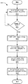
図5Aに、ホストプロセッサを照会する方法の一実施例のフロー図を示す。方法500はホストプロセッサ(アイテム502)の入力レジスタに有効ビットをポーリングすることから開始する。ポーリングの間、有効ビットがクリアな状態であるかあるいはセットされるかどうかについて判断される(アイテム504)。有効ビットがセットされている場合、ポーリングは継続する。セットされる有効ビットはホストプロセッサの入力レジスタがまだ読み出されていない有効データを含むことを表す。テストデータのシリアルローディングは上述のようにTDIピンを介してなされる。テストデータが並列にローディングされるという他の実施例も可能であり、検討される。出力レジスタへのテストデータのローディングに続き、サービスプロセッサの出力ポートはホストプロセッサの入力レジスタにデータを送信し(アイテム508)また有効ビットをセットする(アイテム510)ことができる。ホストプロセッサの入力レジスタに有効ビットをセットすることは有効データが存在し、読み出しの準備ができていることをプロセッサに示す。有効ビットのセットの検出に応答して、ホストプロセッサはテストデータを読み出し、テストデータに基づきステートデータを生成する(アイテム512)。メールボックス入力ポートの入力レジスタに記録される有効ビットは、ホストプロセッサによるテストデータの読み出しに続いてホストプロセッサによりクリアな状態にし得る。
FIG. 5A shows a flow diagram of one embodiment of a method for querying a host processor.
図5Bは、ホストプロセッサからステートデータを出力するための方法の一実施例を示したフロー図である。ステートデータは図5Aで解説された方法及び図1−4において解説された機構により生成される。方法550はホストプロセッサの出力レジスタの有効ビットをポーリングすることから開始する(アイテム552)。図5Aを参照して解説された方法と同様に、有効ビットのポーリングは有効ビットがクリアな状態であると判断されるまで継続される(アイテム554)。有効ビットはクリアな状態であると判断されると、ホストプロセッサはステートデータをそのメールボックス出力ポートの出力レジスタに保存する(556)。出力レジスタへのステートデータのローディングに続いて、ホストプロセッサは出力レジスタに有効ビットをセットする(アイテム560)。サービスプロセッサはCapture-DRステートの有効ビット及びデータを送信し、次いでそれを入力レジスタからシフトする(アイテム562)。送信される有効ビットがセットされる場合、次いでデータは有効であるものとして識別される。入力レジスタからステートデータの読み出しに応答して、ホストプロセッサの有効ビットはクリアすることができ、その結果、追加のステートデータをホストプロセッサから送ることが可能となる。特に、図5Bを参照して解説される演算は、図5Aを参照して解説された演算とは独立して発生可能であることが重要である。
FIG. 5B is a flow diagram illustrating one embodiment of a method for outputting state data from a host processor. The state data is generated by the method described in FIG. 5A and the mechanism described in FIGS. 1-4.
留意すべきは本明細書にて用いられている“テストデータ”という用語は所望の応答を受信するためにホストプロセッサ10に入力されるいずれの種類のデータを参照するということである。同様に、“ステートデータ”という用語はホストプロセッサ10のオペレーションに関する情報を提供するのに用いられるいずれの種類のデータを参照する。加えて更に留意すべきは、テストデータのローディング及び/あるいはステートデータの読み出しはプロセッサの個々の照会に応答するもの、あるいは定期的に実施される演算のうちのどちらか一方である。代替の実施例は可能であり、検討され、有効ビットをポーリングし、データを送信する特定の順序はここに解説されたものと異なってもよい。
It should be noted that the term “test data” as used herein refers to any type of data that is input to the
本発明は特定の実施例に関して解説されているが、実施例は例示的なものであり、発明の範囲は限定されないことが理解されるであろう。実施例のいずれの変形、修正、追加及び改良は可能である。これらの変形、修正、追加、改良は以下のクレームで解説されるように発明の範囲内に収まるものである。 Although the invention has been described with reference to particular embodiments, it will be understood that the embodiments are illustrative and that the scope of the invention is not limited. Any variations, modifications, additions and improvements of the embodiments are possible. These variations, modifications, additions and improvements fall within the scope of the invention as set forth in the following claims.
本発明は、該してプロセッサに応用できる。 The present invention can be applied to a processor.
Claims (10)
前記ホストプロセッサに配置された第1入力レジスタに、第1有効ビットをその第1有効ビットがクリアな状態になるまでポーリングし(502)、
サービスプロセッサに配置された第1出力レジスタにテストデータをロードし(506)、
前記テストデータを前記第1出力レジスタから前記第1入力レジスタへ送信し(508)、
前記送信完了後に前記第1有効ビットをセットし(510)、かつ、
前記第1有効ビットのセットの検出に応答して前記テストデータを前記第1入力レジスタから読み出し(512)、
前記ロード、前記ポーリング、前記送信、前記セット、及び前記読み出しは、前記ホストプロセッサで実行される命令ストリームに割り込みを行わないものである、方法。 A method for determining the state of a host processor, comprising:
Polling a first input register located in the host processor for a first valid bit until the first valid bit is clear (502);
Loading test data into a first output register located in the service processor (506);
Transmitting the test data from the first output register to the first input register (508);
Set the first valid bit (510) after the transmission is completed; and
Reading the test data from the first input register in response to detecting the first set of valid bits (512);
The load, the poll, the send, the set, and the read are those that do not interrupt an instruction stream executed by the host processor.
前記サービスプロセッサへステートデータを出力し、前記ステートデータはホストプロセッサの状態を示すものであり、前記判断及び前記出力は、ホストプロセッサクロックに対し非同期的に実行される、請求項1記載の方法。 Determining the state of the host processor based on the test data; and
The method of claim 1, wherein state data is output to the service processor, the state data indicating a state of a host processor, and the determination and the output are performed asynchronously with respect to a host processor clock.
第2有効ビットを、前記第2有効ビットがクリアな状態になるまで第2出力レジスタにポーリングし(552)、
前記第2出力レジスタにステートデータをロードし(556)、
前記サービスプロセッサに配置された第2入力レジスタに、前記第2出力レジスタから前記ステートデータを送信し(558)かつ、
前記第2入力レジスタから前記ステートデータを出力する(562)、請求項2記載の方法。 The output is
Polling the second output register for a second valid bit until the second valid bit is clear (552);
Loading state data into the second output register (556);
Sending the state data from the second output register to a second input register located in the service processor (558); and
The method of claim 2, wherein the state data is output (562) from the second input register.
前記サービスプロセッサは、前記ホストプロセッサの前記状態を判断するために構成され、
前記判断では、
前記第1入力レジスタの第1有効ビットを前記第1有効ビットがクリアな状態になるまでのポーリング、
前記第1出力レジスタへのテストデータのロード、
前記第1出力レジスタから前記第1入力レジスタへの前記テストデータの送信、
前記送信完了後での前記第1有効ビットのセット、がなされ、
前記ホストプロセッサは、前記第1有効ビットに応答して、前記第1入力レジスタから前記テストデータを読み出すように構成されたものであり、かつ、
前記ロード、前記ポーリング、前記送信、前記セット、前記読み出しは、前記ホストプロセッサで実行する命令ストリームに割り込みを行わないものである、システム。 A host processor (10) and a service processor (140), the host processor comprising a first input register (102), the service processor comprising a first output register (152), and the host processor comprising a second input register (152); The output register (104), the service processor comprises a second input register (154),
The service processor is configured to determine the state of the host processor;
In the judgment,
Polling the first valid bit of the first input register until the first valid bit is cleared;
Loading test data into the first output register;
Transmitting the test data from the first output register to the first input register;
The first valid bit is set after the transmission is completed,
The host processor is configured to read the test data from the first input register in response to the first valid bit; and
The load, the poll, the transmission, the set, and the read do not interrupt an instruction stream executed by the host processor.
前記テストデータに基づきホストプロセッサの状態を判断し、かつ、
前記サービスプロセッサにステートデータを出力するよう構成されたものであり、前記ステートデータは、ホストプロセッサの状態を示し、前記判断及び出力は、前記ホストプロセッサクロックに対し非同期的に実行される、請求項6記載のシステム。 The host processor further includes:
Determining the state of the host processor based on the test data; and
The system is configured to output state data to the service processor, wherein the state data indicates a state of a host processor, and the determination and output are executed asynchronously with respect to the host processor clock. 6. The system according to 6.
前記第2出力レジスタの第2有効ビットを前記第2有効ビットがクリアな状態になるまでポーリングし、
前記第2出力レジスタにステートデータを保存し、
前記第2出力レジスタから前記第2入力レジスタへとステートデータを送信するように構成され、前記サービスプロセッサは、前記第2入力レジスタにより受信される前記ステートデータを出力するように構成される、請求項7記載のシステム。 The host processor further includes:
Polling the second valid bit of the second output register until the second valid bit is clear;
Storing state data in the second output register;
The state processor is configured to transmit state data from the second output register to the second input register, and the service processor is configured to output the state data received by the second input register. Item 8. The system according to Item 7.
Applications Claiming Priority (2)
| Application Number | Priority Date | Filing Date | Title |
|---|---|---|---|
| US19383602A | 2002-07-11 | 2002-07-11 | |
| PCT/US2003/021288 WO2004008319A2 (en) | 2002-07-11 | 2003-07-09 | Method and apparatus for determining a processor state without interrupting processor operation |
Publications (1)
| Publication Number | Publication Date |
|---|---|
| JP2006514349A true JP2006514349A (en) | 2006-04-27 |
Family
ID=30114619
Family Applications (1)
| Application Number | Title | Priority Date | Filing Date |
|---|---|---|---|
| JP2004521558A Withdrawn JP2006514349A (en) | 2002-07-11 | 2003-07-09 | Method and apparatus for determining processor state without interfering with processor operation |
Country Status (6)
| Country | Link |
|---|---|
| EP (1) | EP1576475A2 (en) |
| JP (1) | JP2006514349A (en) |
| CN (1) | CN1669004A (en) |
| AU (1) | AU2003261128A1 (en) |
| TW (1) | TW200401194A (en) |
| WO (1) | WO2004008319A2 (en) |
Families Citing this family (4)
| Publication number | Priority date | Publication date | Assignee | Title |
|---|---|---|---|---|
| TW201018678A (en) | 2006-01-27 | 2010-05-16 | Astrazeneca Ab | Novel heteroaryl substituted benzothiazoles |
| TW200813035A (en) | 2006-06-19 | 2008-03-16 | Astrazeneca Ab | Novel heteroaryl substituted benzoxazoles |
| TW200901998A (en) | 2007-03-06 | 2009-01-16 | Astrazeneca Ab | Novel 2-heteroaryl substituted benzothiophenes and benzofuranes |
| CN102621483B (en) * | 2012-03-27 | 2014-04-16 | 中国人民解放军国防科学技术大学 | Multi-link parallel boundary scanning testing device and method |
Family Cites Families (3)
| Publication number | Priority date | Publication date | Assignee | Title |
|---|---|---|---|---|
| EP0636976B1 (en) * | 1993-07-28 | 1998-12-30 | Koninklijke Philips Electronics N.V. | Microcontroller provided with hardware for supporting debugging as based on boundary scan standard-type extensions |
| US5444716A (en) * | 1993-08-30 | 1995-08-22 | At&T Corp. | Boundary-scan-based system and method for test and diagnosis |
| US6115763A (en) * | 1998-03-05 | 2000-09-05 | International Business Machines Corporation | Multi-core chip providing external core access with regular operation function interface and predetermined service operation services interface comprising core interface units and masters interface unit |
-
2003
- 2003-07-04 TW TW92118292A patent/TW200401194A/en unknown
- 2003-07-09 WO PCT/US2003/021288 patent/WO2004008319A2/en not_active Ceased
- 2003-07-09 JP JP2004521558A patent/JP2006514349A/en not_active Withdrawn
- 2003-07-09 CN CN 03816538 patent/CN1669004A/en active Pending
- 2003-07-09 AU AU2003261128A patent/AU2003261128A1/en not_active Abandoned
- 2003-07-09 EP EP03764379A patent/EP1576475A2/en not_active Withdrawn
Also Published As
| Publication number | Publication date |
|---|---|
| AU2003261128A8 (en) | 2004-02-02 |
| TW200401194A (en) | 2004-01-16 |
| EP1576475A2 (en) | 2005-09-21 |
| WO2004008319A3 (en) | 2004-05-21 |
| CN1669004A (en) | 2005-09-14 |
| AU2003261128A1 (en) | 2004-02-02 |
| WO2004008319A2 (en) | 2004-01-22 |
Similar Documents
| Publication | Publication Date | Title |
|---|---|---|
| JP3871884B2 (en) | Mechanism for memory-to-load transfers | |
| US6065103A (en) | Speculative store buffer | |
| US6880073B2 (en) | Speculative execution of instructions and processes before completion of preceding barrier operations | |
| US5933626A (en) | Apparatus and method for tracing microprocessor instructions | |
| EP1228426B1 (en) | Store buffer which forwards data based on index and optional way match | |
| US8069336B2 (en) | Transitioning from instruction cache to trace cache on label boundaries | |
| US7003629B1 (en) | System and method of identifying liveness groups within traces stored in a trace cache | |
| EP0628184B1 (en) | Cpu having pipelined instruction unit and effective address calculation unit with retained virtual address capability | |
| US5941981A (en) | System for using a data history table to select among multiple data prefetch algorithms | |
| AU628527B2 (en) | Virtual instruction cache refill algorithm | |
| US6088789A (en) | Prefetch instruction specifying destination functional unit and read/write access mode | |
| US6622237B1 (en) | Store to load forward predictor training using delta tag | |
| US6651161B1 (en) | Store load forward predictor untraining | |
| US6425090B1 (en) | Method for just-in-time delivery of load data utilizing alternating time intervals | |
| US20090024842A1 (en) | Precise Counter Hardware for Microcode Loops | |
| KR100698493B1 (en) | Method and apparatus for performing calculations on narrow operands | |
| JP2005500616A (en) | Branch prediction with 2-level branch prediction cache | |
| KR19990072271A (en) | High performance speculative misaligned load operations | |
| KR20000070468A (en) | A line-oriented reorder buffer for a superscalar microprocessor | |
| US6934903B1 (en) | Using microcode to correct ECC errors in a processor | |
| US6230262B1 (en) | Processor configured to selectively free physical registers upon retirement of instructions | |
| US6332187B1 (en) | Cumulative lookahead to eliminate chained dependencies | |
| KR101466934B1 (en) | Distributed dispatch using concurrent, non-sequential dispatch | |
| US6704854B1 (en) | Determination of execution resource allocation based on concurrently executable misaligned memory operations | |
| US7694110B1 (en) | System and method of implementing microcode operations as subroutines |
Legal Events
| Date | Code | Title | Description |
|---|---|---|---|
| A300 | Application deemed to be withdrawn because no request for examination was validly filed |
Free format text: JAPANESE INTERMEDIATE CODE: A300 Effective date: 20061003 |