JP2006511046A - Phosphors passivated with aluminum nitride for electroluminescent displays - Google Patents
Phosphors passivated with aluminum nitride for electroluminescent displays Download PDFInfo
- Publication number
- JP2006511046A JP2006511046A JP2004560943A JP2004560943A JP2006511046A JP 2006511046 A JP2006511046 A JP 2006511046A JP 2004560943 A JP2004560943 A JP 2004560943A JP 2004560943 A JP2004560943 A JP 2004560943A JP 2006511046 A JP2006511046 A JP 2006511046A
- Authority
- JP
- Japan
- Prior art keywords
- aluminum nitride
- phosphor
- activated
- film
- fluorescent
- Prior art date
- Legal status (The legal status is an assumption and is not a legal conclusion. Google has not performed a legal analysis and makes no representation as to the accuracy of the status listed.)
- Pending
Links
Images


Classifications
-
- C—CHEMISTRY; METALLURGY
- C09—DYES; PAINTS; POLISHES; NATURAL RESINS; ADHESIVES; COMPOSITIONS NOT OTHERWISE PROVIDED FOR; APPLICATIONS OF MATERIALS NOT OTHERWISE PROVIDED FOR
- C09K—MATERIALS FOR MISCELLANEOUS APPLICATIONS, NOT PROVIDED FOR ELSEWHERE
- C09K11/00—Luminescent materials, e.g. electroluminescent or chemiluminescent
- C09K11/02—Use of particular materials as binders, particle coatings or suspension media therefor
-
- C—CHEMISTRY; METALLURGY
- C09—DYES; PAINTS; POLISHES; NATURAL RESINS; ADHESIVES; COMPOSITIONS NOT OTHERWISE PROVIDED FOR; APPLICATIONS OF MATERIALS NOT OTHERWISE PROVIDED FOR
- C09K—MATERIALS FOR MISCELLANEOUS APPLICATIONS, NOT PROVIDED FOR ELSEWHERE
- C09K11/00—Luminescent materials, e.g. electroluminescent or chemiluminescent
- C09K11/08—Luminescent materials, e.g. electroluminescent or chemiluminescent containing inorganic luminescent materials
- C09K11/77—Luminescent materials, e.g. electroluminescent or chemiluminescent containing inorganic luminescent materials containing rare earth metals
-
- C—CHEMISTRY; METALLURGY
- C09—DYES; PAINTS; POLISHES; NATURAL RESINS; ADHESIVES; COMPOSITIONS NOT OTHERWISE PROVIDED FOR; APPLICATIONS OF MATERIALS NOT OTHERWISE PROVIDED FOR
- C09K—MATERIALS FOR MISCELLANEOUS APPLICATIONS, NOT PROVIDED FOR ELSEWHERE
- C09K11/00—Luminescent materials, e.g. electroluminescent or chemiluminescent
- C09K11/08—Luminescent materials, e.g. electroluminescent or chemiluminescent containing inorganic luminescent materials
- C09K11/57—Luminescent materials, e.g. electroluminescent or chemiluminescent containing inorganic luminescent materials containing manganese or rhenium
- C09K11/572—Chalcogenides
- C09K11/574—Chalcogenides with zinc or cadmium
-
- C—CHEMISTRY; METALLURGY
- C09—DYES; PAINTS; POLISHES; NATURAL RESINS; ADHESIVES; COMPOSITIONS NOT OTHERWISE PROVIDED FOR; APPLICATIONS OF MATERIALS NOT OTHERWISE PROVIDED FOR
- C09K—MATERIALS FOR MISCELLANEOUS APPLICATIONS, NOT PROVIDED FOR ELSEWHERE
- C09K11/00—Luminescent materials, e.g. electroluminescent or chemiluminescent
- C09K11/08—Luminescent materials, e.g. electroluminescent or chemiluminescent containing inorganic luminescent materials
- C09K11/77—Luminescent materials, e.g. electroluminescent or chemiluminescent containing inorganic luminescent materials containing rare earth metals
- C09K11/7701—Chalogenides
- C09K11/7702—Chalogenides with zinc or cadmium
-
- C—CHEMISTRY; METALLURGY
- C09—DYES; PAINTS; POLISHES; NATURAL RESINS; ADHESIVES; COMPOSITIONS NOT OTHERWISE PROVIDED FOR; APPLICATIONS OF MATERIALS NOT OTHERWISE PROVIDED FOR
- C09K—MATERIALS FOR MISCELLANEOUS APPLICATIONS, NOT PROVIDED FOR ELSEWHERE
- C09K11/00—Luminescent materials, e.g. electroluminescent or chemiluminescent
- C09K11/08—Luminescent materials, e.g. electroluminescent or chemiluminescent containing inorganic luminescent materials
- C09K11/77—Luminescent materials, e.g. electroluminescent or chemiluminescent containing inorganic luminescent materials containing rare earth metals
- C09K11/7701—Chalogenides
- C09K11/7703—Chalogenides with alkaline earth metals
-
- C—CHEMISTRY; METALLURGY
- C09—DYES; PAINTS; POLISHES; NATURAL RESINS; ADHESIVES; COMPOSITIONS NOT OTHERWISE PROVIDED FOR; APPLICATIONS OF MATERIALS NOT OTHERWISE PROVIDED FOR
- C09K—MATERIALS FOR MISCELLANEOUS APPLICATIONS, NOT PROVIDED FOR ELSEWHERE
- C09K11/00—Luminescent materials, e.g. electroluminescent or chemiluminescent
- C09K11/08—Luminescent materials, e.g. electroluminescent or chemiluminescent containing inorganic luminescent materials
- C09K11/77—Luminescent materials, e.g. electroluminescent or chemiluminescent containing inorganic luminescent materials containing rare earth metals
- C09K11/7706—Aluminates
-
- C—CHEMISTRY; METALLURGY
- C09—DYES; PAINTS; POLISHES; NATURAL RESINS; ADHESIVES; COMPOSITIONS NOT OTHERWISE PROVIDED FOR; APPLICATIONS OF MATERIALS NOT OTHERWISE PROVIDED FOR
- C09K—MATERIALS FOR MISCELLANEOUS APPLICATIONS, NOT PROVIDED FOR ELSEWHERE
- C09K11/00—Luminescent materials, e.g. electroluminescent or chemiluminescent
- C09K11/08—Luminescent materials, e.g. electroluminescent or chemiluminescent containing inorganic luminescent materials
- C09K11/77—Luminescent materials, e.g. electroluminescent or chemiluminescent containing inorganic luminescent materials containing rare earth metals
- C09K11/7715—Luminescent materials, e.g. electroluminescent or chemiluminescent containing inorganic luminescent materials containing rare earth metals containing cerium
- C09K11/7716—Chalcogenides
- C09K11/7718—Chalcogenides with alkaline earth metals
-
- C—CHEMISTRY; METALLURGY
- C09—DYES; PAINTS; POLISHES; NATURAL RESINS; ADHESIVES; COMPOSITIONS NOT OTHERWISE PROVIDED FOR; APPLICATIONS OF MATERIALS NOT OTHERWISE PROVIDED FOR
- C09K—MATERIALS FOR MISCELLANEOUS APPLICATIONS, NOT PROVIDED FOR ELSEWHERE
- C09K11/00—Luminescent materials, e.g. electroluminescent or chemiluminescent
- C09K11/08—Luminescent materials, e.g. electroluminescent or chemiluminescent containing inorganic luminescent materials
- C09K11/77—Luminescent materials, e.g. electroluminescent or chemiluminescent containing inorganic luminescent materials containing rare earth metals
- C09K11/7728—Luminescent materials, e.g. electroluminescent or chemiluminescent containing inorganic luminescent materials containing rare earth metals containing europium
- C09K11/7729—Chalcogenides
- C09K11/773—Chalcogenides with zinc or cadmium
-
- C—CHEMISTRY; METALLURGY
- C09—DYES; PAINTS; POLISHES; NATURAL RESINS; ADHESIVES; COMPOSITIONS NOT OTHERWISE PROVIDED FOR; APPLICATIONS OF MATERIALS NOT OTHERWISE PROVIDED FOR
- C09K—MATERIALS FOR MISCELLANEOUS APPLICATIONS, NOT PROVIDED FOR ELSEWHERE
- C09K11/00—Luminescent materials, e.g. electroluminescent or chemiluminescent
- C09K11/08—Luminescent materials, e.g. electroluminescent or chemiluminescent containing inorganic luminescent materials
- C09K11/77—Luminescent materials, e.g. electroluminescent or chemiluminescent containing inorganic luminescent materials containing rare earth metals
- C09K11/7728—Luminescent materials, e.g. electroluminescent or chemiluminescent containing inorganic luminescent materials containing rare earth metals containing europium
- C09K11/7729—Chalcogenides
- C09K11/7731—Chalcogenides with alkaline earth metals
-
- C—CHEMISTRY; METALLURGY
- C09—DYES; PAINTS; POLISHES; NATURAL RESINS; ADHESIVES; COMPOSITIONS NOT OTHERWISE PROVIDED FOR; APPLICATIONS OF MATERIALS NOT OTHERWISE PROVIDED FOR
- C09K—MATERIALS FOR MISCELLANEOUS APPLICATIONS, NOT PROVIDED FOR ELSEWHERE
- C09K11/00—Luminescent materials, e.g. electroluminescent or chemiluminescent
- C09K11/08—Luminescent materials, e.g. electroluminescent or chemiluminescent containing inorganic luminescent materials
- C09K11/77—Luminescent materials, e.g. electroluminescent or chemiluminescent containing inorganic luminescent materials containing rare earth metals
- C09K11/7728—Luminescent materials, e.g. electroluminescent or chemiluminescent containing inorganic luminescent materials containing rare earth metals containing europium
- C09K11/7734—Aluminates
-
- C—CHEMISTRY; METALLURGY
- C09—DYES; PAINTS; POLISHES; NATURAL RESINS; ADHESIVES; COMPOSITIONS NOT OTHERWISE PROVIDED FOR; APPLICATIONS OF MATERIALS NOT OTHERWISE PROVIDED FOR
- C09K—MATERIALS FOR MISCELLANEOUS APPLICATIONS, NOT PROVIDED FOR ELSEWHERE
- C09K11/00—Luminescent materials, e.g. electroluminescent or chemiluminescent
- C09K11/08—Luminescent materials, e.g. electroluminescent or chemiluminescent containing inorganic luminescent materials
- C09K11/77—Luminescent materials, e.g. electroluminescent or chemiluminescent containing inorganic luminescent materials containing rare earth metals
- C09K11/7743—Luminescent materials, e.g. electroluminescent or chemiluminescent containing inorganic luminescent materials containing rare earth metals containing terbium
- C09K11/7744—Chalcogenides
- C09K11/7745—Chalcogenides with zinc or cadmium
-
- C—CHEMISTRY; METALLURGY
- C09—DYES; PAINTS; POLISHES; NATURAL RESINS; ADHESIVES; COMPOSITIONS NOT OTHERWISE PROVIDED FOR; APPLICATIONS OF MATERIALS NOT OTHERWISE PROVIDED FOR
- C09K—MATERIALS FOR MISCELLANEOUS APPLICATIONS, NOT PROVIDED FOR ELSEWHERE
- C09K11/00—Luminescent materials, e.g. electroluminescent or chemiluminescent
- C09K11/08—Luminescent materials, e.g. electroluminescent or chemiluminescent containing inorganic luminescent materials
- C09K11/88—Luminescent materials, e.g. electroluminescent or chemiluminescent containing inorganic luminescent materials containing selenium, tellurium or unspecified chalcogen elements
- C09K11/881—Chalcogenides
- C09K11/883—Chalcogenides with zinc or cadmium
-
- C—CHEMISTRY; METALLURGY
- C09—DYES; PAINTS; POLISHES; NATURAL RESINS; ADHESIVES; COMPOSITIONS NOT OTHERWISE PROVIDED FOR; APPLICATIONS OF MATERIALS NOT OTHERWISE PROVIDED FOR
- C09K—MATERIALS FOR MISCELLANEOUS APPLICATIONS, NOT PROVIDED FOR ELSEWHERE
- C09K11/00—Luminescent materials, e.g. electroluminescent or chemiluminescent
- C09K11/08—Luminescent materials, e.g. electroluminescent or chemiluminescent containing inorganic luminescent materials
- C09K11/88—Luminescent materials, e.g. electroluminescent or chemiluminescent containing inorganic luminescent materials containing selenium, tellurium or unspecified chalcogen elements
- C09K11/881—Chalcogenides
- C09K11/886—Chalcogenides with rare earth metals
-
- H—ELECTRICITY
- H05—ELECTRIC TECHNIQUES NOT OTHERWISE PROVIDED FOR
- H05B—ELECTRIC HEATING; ELECTRIC LIGHT SOURCES NOT OTHERWISE PROVIDED FOR; CIRCUIT ARRANGEMENTS FOR ELECTRIC LIGHT SOURCES, IN GENERAL
- H05B33/00—Electroluminescent light sources
- H05B33/10—Apparatus or processes specially adapted to the manufacture of electroluminescent light sources
-
- H—ELECTRICITY
- H05—ELECTRIC TECHNIQUES NOT OTHERWISE PROVIDED FOR
- H05B—ELECTRIC HEATING; ELECTRIC LIGHT SOURCES NOT OTHERWISE PROVIDED FOR; CIRCUIT ARRANGEMENTS FOR ELECTRIC LIGHT SOURCES, IN GENERAL
- H05B33/00—Electroluminescent light sources
- H05B33/12—Light sources with substantially two-dimensional [2D] radiating surfaces
- H05B33/14—Light sources with substantially two-dimensional [2D] radiating surfaces characterised by the chemical or physical composition or the arrangement of the electroluminescent material, or by the simultaneous addition of the electroluminescent material in or onto the light source
-
- H—ELECTRICITY
- H05—ELECTRIC TECHNIQUES NOT OTHERWISE PROVIDED FOR
- H05B—ELECTRIC HEATING; ELECTRIC LIGHT SOURCES NOT OTHERWISE PROVIDED FOR; CIRCUIT ARRANGEMENTS FOR ELECTRIC LIGHT SOURCES, IN GENERAL
- H05B33/00—Electroluminescent light sources
- H05B33/12—Light sources with substantially two-dimensional [2D] radiating surfaces
- H05B33/22—Light sources with substantially two-dimensional [2D] radiating surfaces characterised by the chemical or physical composition or the arrangement of auxiliary dielectric or reflective layers
-
- Y—GENERAL TAGGING OF NEW TECHNOLOGICAL DEVELOPMENTS; GENERAL TAGGING OF CROSS-SECTIONAL TECHNOLOGIES SPANNING OVER SEVERAL SECTIONS OF THE IPC; TECHNICAL SUBJECTS COVERED BY FORMER USPC CROSS-REFERENCE ART COLLECTIONS [XRACs] AND DIGESTS
- Y10—TECHNICAL SUBJECTS COVERED BY FORMER USPC
- Y10S—TECHNICAL SUBJECTS COVERED BY FORMER USPC CROSS-REFERENCE ART COLLECTIONS [XRACs] AND DIGESTS
- Y10S428/00—Stock material or miscellaneous articles
- Y10S428/917—Electroluminescent
-
- Y—GENERAL TAGGING OF NEW TECHNOLOGICAL DEVELOPMENTS; GENERAL TAGGING OF CROSS-SECTIONAL TECHNOLOGIES SPANNING OVER SEVERAL SECTIONS OF THE IPC; TECHNICAL SUBJECTS COVERED BY FORMER USPC CROSS-REFERENCE ART COLLECTIONS [XRACs] AND DIGESTS
- Y10—TECHNICAL SUBJECTS COVERED BY FORMER USPC
- Y10T—TECHNICAL SUBJECTS COVERED BY FORMER US CLASSIFICATION
- Y10T428/00—Stock material or miscellaneous articles
- Y10T428/26—Web or sheet containing structurally defined element or component, the element or component having a specified physical dimension
Landscapes
- Chemical & Material Sciences (AREA)
- Engineering & Computer Science (AREA)
- Materials Engineering (AREA)
- Organic Chemistry (AREA)
- Inorganic Chemistry (AREA)
- Manufacturing & Machinery (AREA)
- Electroluminescent Light Sources (AREA)
- Luminescent Compositions (AREA)
Abstract
AC厚膜誘電性エレクトロルミネッセンスデバイスに用いられる輝度及び動作安定性を改善した新規な構造体が提供されている。 この新規な構造体は、酸素との反応に起因する蛍光物質の劣化を防止するために、蛍光膜に接触している窒化アルミニウムのバリア層を有している。 このバリア層は、蛍光膜を蒸着及び焼鈍するために使用される工程と互換性のある真空蒸着工程を使用して蒸着することができる。 本発明は、蛍光膜を形成及び活性化するために高い工程温度にさらされる厚い誘電体層を採用しているエレクトロルミネッセンスディスプレイにおいて使用される蛍光物質に特に好適である。Novel structures with improved brightness and operational stability for use in AC thick film dielectric electroluminescent devices are provided. This novel structure has an aluminum nitride barrier layer in contact with the phosphor film to prevent degradation of the phosphor due to reaction with oxygen. This barrier layer can be deposited using a vacuum deposition process that is compatible with the process used to deposit and anneal the phosphor film. The present invention is particularly suitable for phosphors used in electroluminescent displays that employ thick dielectric layers that are exposed to high process temperatures to form and activate phosphor films.
Description
本発明は、高い誘電率の厚膜誘電体層を使用しているフルカラーACエレクトロルミネッセンスディスプレイ(electroluminescent displays)に用いられる蛍光物質(phosphors)の輝度及び動作安定性の改善に関するものである。
より具体的には本発明は、厚膜誘電性エレクトロルミネッセンスディスプレイ(thick film dielectric electroluminescent display)において、蛍光物質が酸素及び他の有害な種と反応することを最小化あるいは防止するために、蛍光膜と接触している窒化アルミニウムのバリア層を提供するものである。
The present invention relates to improving the brightness and operational stability of phosphors used in full color AC electroluminescent displays using a thick dielectric layer with a high dielectric constant.
More specifically, the present invention relates to a phosphor film in a thick film dielectric electroluminescent display in order to minimize or prevent the phosphor from reacting with oxygen and other harmful species. An aluminum nitride barrier layer in contact with the substrate is provided.
特許文献1(引用により、その全体が本明細書に組み込まれる。)に例示されている厚膜誘電体構造が知られており、従前の薄膜エレクトロルミネッセンス(thin film electroluminescent:TFEL)ディスプレイに対して優れた特性を発揮する。
高性能の赤、緑、青の蛍光体材料が、厚膜誘電体構造用として増大された輝度特性を提供するべく開発されている。
これらの蛍光体材料は、青色を発するためのユーロピウム(europium)で活性化されたバリウム・チオアルミ酸塩(barium thioaluminate)ベースの材料と、緑色を発するためのテルビウム(terbium)で活性化された硫化亜鉛、マンガンで活性化されたマグネシウム硫化亜鉛(magnesium zinc sulfide)あるいはユーロピウムで活性化されたカルシウム・チオアルミ酸塩(calcium thioaluminate)ベースの材料と、赤色を発するために適宜フィルタをかけられる従前のマンガンで活性化された硫化亜鉛と、を含んでいる。
A thick film dielectric structure is known which is illustrated in US Pat. No. 6,057,028 (incorporated herein by reference in its entirety), for a conventional thin film electroluminescent (TFEL) display. Exhibits excellent properties.
High performance red, green and blue phosphor materials have been developed to provide increased brightness characteristics for thick film dielectric structures.
These phosphor materials are based on a barium thioaluminate-based material activated with europium to emit blue and terbium activated sulfide to emit green Zinc, manganese activated magnesium zinc sulfide or europium activated calcium thioaluminate based material, and conventional manganese filtered appropriately to produce a red color And activated by zinc sulfide.
高輝度フルカラー厚膜誘電性エレクトロルミネッセンスディスプレイは赤、緑、青のサブピクセルがパターン形成されるための薄膜蛍光体材料を必要とし、ピクセルの各色は、各サブピクセルについて要求される色座標を達成するために必要な光フィルタの使用に伴う減衰を最小化するように合わせられている。
相対的に低い解像度のディスプレイについては、パターン形成はシャドーマスクを通じて蛍光体材料を蒸着することにより行われる。
しかしながら高解像度ディスプレイについては、シャドーマスク技術ではフォトリソグラフィック法の採用が要求されるような十分な精度を提供することができない。
特許文献2(引用により、その全体が本明細書に組み込まれる。)に例示されているようにフォトリソグラフィック技術は、要求されるパターンを提供するためにフォトレジスト膜の蒸着、及び蛍光膜の一部をエッチングあるいは剥離させることを必要とする。
フォトレジスト膜の蒸着及び除去と、蛍光膜のエッチングまたは剥離には、水あるいはその他のプロトン性溶媒(protic solvents)を含有する溶剤を必要とする。
工程雰囲気中に存在しうる水分あるいは酸素の反応を伴うフォトリソグラフィック工程の後に、ディスプレイ構造体に残存しているこれら溶剤の残留分(traces)は、完成品のディスプレイの性能劣化を生じる酸化反応あるいは加水分解反応に対して敏感な特定の蛍光体材料と化学的に反応する場合がある。
ディスプレイの動作中の連続する化学反応は、継続的な性能劣化を生じ、これによりディスプレイの寿命が短くなる場合がある。
High-brightness full-color thick-film dielectric electroluminescent displays require thin-film phosphor materials for the red, green, and blue subpixels to be patterned, and each color of the pixel achieves the required color coordinates for each subpixel It is tailored to minimize the attenuation associated with the use of the optical filter required.
For relatively low resolution displays, patterning is done by depositing phosphor material through a shadow mask.
However, for high-resolution displays, shadow mask technology cannot provide sufficient accuracy that requires the adoption of photolithographic methods.
As illustrated in U.S. Pat. No. 6,057,028 (incorporated herein by reference in its entirety), photolithographic techniques involve the deposition of photoresist films and one of the phosphor films to provide the required pattern. It is necessary to etch or peel off the part.
The deposition and removal of the photoresist film and the etching or stripping of the fluorescent film require a solvent containing water or other protic solvents.
After photolithographic processes involving the reaction of moisture or oxygen that may be present in the process atmosphere, these solvent traces remaining in the display structure are responsible for oxidation reactions or degradations that cause performance degradation of the finished display. It may react chemically with certain phosphor materials that are sensitive to hydrolysis reactions.
Continuous chemical reactions during the operation of the display can result in continuous performance degradation, which can shorten the life of the display.
かかる性能劣化の問題を解消するために、特定の蛍光体材料と共に用いる種々の材料が提案されている。
テルビウムで活性化された硫化亜鉛及び硫化マグネシウム亜鉛の蛍光物質と共に用いるために、窒化珪素が提案されている(非特許文献1、非特許文献2)。
In order to solve the problem of such performance deterioration, various materials used together with a specific phosphor material have been proposed.
Silicon nitride has been proposed for use with phosphors of zinc sulfide and magnesium zinc sulfide activated with terbium (Non-Patent Documents 1 and 2).
特許文献3、特許文献4、特許文献5及び特許文献6には、プラズマCVD法(plasma chemical vapour deposition method)を用いて蒸着された硫化マグネシウム亜鉛の蛍光膜と共に用いられる窒化珪素層あるいは酸窒化珪素層(silicon oxynitride layers)が開示されている。
特許文献7及び特許文献8には、テルビウムがドーピングされたエレクトロルミネッセンスディスプレイ用の硫化亜鉛が開示されている。
また、特許文献9には、硫化亜鉛の拡散バリア層(diffusion barrier layer)を有する希土類で活性化された硫化亜鉛材料を含むエレクトロルミネッセンス積層体が開示されている。
Patent Document 9 discloses an electroluminescent laminate including a rare earth activated zinc sulfide material having a zinc sulfide diffusion barrier layer.
また、特許文献10及び特許文献11に記載されているような薄膜エレクトロルミネッセンスデバイスにおけるアルカリ土類カルコゲン(alkali earth chalcogen)のEL発光層と共に用いるための窒化アルミニウムも提案されている。
また、窒化アルミニウムは、特許文献12、特許文献13、特許文献14、特許文献15及び特許文献16に記載されているような有機エレクトロルミネッセンスデバイス/ディスプレイにおける絶縁薄膜層として用いられるだけでなく、特許文献17及び特許文献18に記載されているようなEL素子における水分のバリア層としても用いられている。
また、特許文献19に開示されているように、セラミック基板としての窒化アルミニウムも提案されている。
Also proposed are aluminum nitrides for use with alkaline earth chalcogen EL light emitting layers in thin film electroluminescent devices such as those described in US Pat.
Aluminum nitride is not only used as an insulating thin film layer in organic electroluminescence devices / displays as described in
Further, as disclosed in Patent Document 19, aluminum nitride as a ceramic substrate has also been proposed.
特許文献20は、従前のマンガンで活性化されたマグネシウム硫化亜鉛蛍光膜と厚膜誘電体層との間に設けられる半導体材料としての窒化アルミニウムの使用を開示している。
このようなデバイスは、蛍光膜を焼鈍し、窒化アルミニウムの層を焼鈍された蛍光物質の上に形成し、そしてスクリーン印刷と厚膜誘電体層とをその上に形成して、窒化アルミニウムが蛍光膜と厚膜誘電体層との間に配置されるように構成されている。
Such a device anneals the phosphor film, forms a layer of aluminum nitride on the annealed phosphor, and forms a screen print and a thick film dielectric layer thereon so that the aluminum nitride is fluorescent. It is configured to be disposed between the film and the thick dielectric layer.
前掲の特許及び特許出願は、従前の硫化亜鉛蛍光物質と共に、あるいは薄膜エレクトロルミネッセンスディスプレイ内で用いられる窒化アルミニウムのような特定の絶縁材料の使用を教示しているかもしれないが、性能劣化を最小限として改善された輝度及び動作寿命を発揮する厚膜誘電性エレクトロルミネッセンスディスプレイ内で使用するために特に改良した蛍光体材料の要請は依然として存在している。
本発明は、厚膜誘電性エレクトロルミネッセンスデバイス内に設けられる蛍光物質と共に使用するためのパッシベーション層あるいはバリア層に関するものである。 The present invention relates to a passivation layer or barrier layer for use with a fluorescent material provided in a thick film dielectric electroluminescent device.
より具体的には、本発明は蛍光物質と共に使用されるパッシベーション層あるいはバリア層であって、希土類で活性化されたバリウム・チオアルミ酸塩(barium thioaluminate)、希土類で活性化された微粒状の硫化亜鉛、遷移金属で活性化された硫化亜鉛、希土類または遷移金属で活性化されたセレン化亜鉛(zinc selenide)、及び希土類または遷移金属で活性化されたスルホセレン化亜鉛(zinc sulfo-selenide)のうちから選択されることを特徴とするものである。
蛍光物質は、例えば本出願人による特許文献1及び本出願人により2002年12月21日に出願された米国特許出願第60/341,790号明細書(これらは、引用により、その全体が本明細書に組み込まれる。)に記載されているような厚膜誘電性エレクトロルミネッセンスデバイス内で使用される蛍光物質である。
More specifically, the present invention is a passivation layer or barrier layer used with a fluorescent material, which is a rare earth activated barium thioaluminate, a rare earth activated fine particulate sulfide. Of zinc, transition metal activated zinc sulfide, rare earth or transition metal activated zinc selenide, and rare earth or transition metal activated zinc selenide It is selected from these.
The fluorescent material is disclosed in, for example, US Pat. No. 60 / 341,790 filed on Dec. 21, 2002 by the present applicant and US Pat. No. 60 / 341,790 filed by the present applicant. A fluorescent material used in thick film dielectric electroluminescent devices as described in.
本発明のバリア層は、蛍光物質の輝度及び動作寿命を改善するのに寄与するものである。
このバリア層は、(側面視で)蛍光膜の上側及び任意的に蛍光膜の下側に形成された一以上の窒化アルミニウム層を有している。
本発明の好ましい観点において、このバリア層は、蛍光体材料の観察している側面にも形成されている。
The barrier layer of the present invention contributes to improving the luminance and operating life of the fluorescent material.
The barrier layer has (at a side view) one or more aluminum nitride layers formed above the phosphor film and optionally below the phosphor film.
In a preferred aspect of the present invention, this barrier layer is also formed on the side of the phosphor material being observed.
本発明のバリア層は、デバイス内に存在するあらゆる化学種(chemical species)が蛍光物質と反応することを防止あるいは反応を最小化するように作用するものである。
このような化学種は、発光する蛍光物質における活性化種(activator species)と電子とが相互に作用する効率の低下を引き起こすことにより、電子がデバイスの動作中に蛍光物質内へ注入される効率の低下を生じてしまい、蛍光物質の実現可能な輝度の低下を生じる場合がある。
また、化学種は蛍光物質内で生成される光が有用な輝度を提供するためにデバイスから伝達される効率を低下させるように作用してしまう。
The barrier layer of the present invention acts to prevent or minimize reaction of any chemical species present in the device with the fluorescent material.
Such chemical species cause the efficiency of electrons to be injected into the phosphor during device operation by causing a reduction in the efficiency of interaction between the activator species and the electrons in the phosphor that emits light. May result in a decrease in the luminance that can be achieved by the fluorescent material.
Chemical species also act to reduce the efficiency with which the light produced in the fluorescent material is transmitted from the device to provide useful brightness.
とりわけ、蛍光物質の劣化は酸素あるいは水分との反応を伴うので、少なくとも蛍光物質の一部の化学的な組成が変化してしまう。
本発明の窒化アルミニウムのパッシベーション層は、蛍光層の外表面に、例えば、デバイスの厚い誘電体構造、蛍光物質をパターン形成するために使用されるフォトリソグラフィック工程で用いられる化学物質の残留種(residual species)、若しくは隣接する薄膜層に由来する酸素、及び/または外部環境に由来する酸素に対するバリアとして機能するものである。
In particular, since the deterioration of the fluorescent material is accompanied by a reaction with oxygen or moisture, at least a part of the chemical composition of the fluorescent material changes.
The aluminum nitride passivation layer of the present invention is formed on the outer surface of the phosphor layer, for example, the thick dielectric structure of the device, the residual species of chemicals used in photolithographic processes used to pattern phosphors. species) or oxygen derived from adjacent thin film layers and / or as a barrier to oxygen derived from the external environment.
バリア層の材料は、隣接する層、特に蛍光体材料と化学反応を生じないように選択されている。
ディスプレイデバイスの動作のため、及び動作中の製造工程の間の化学的な反応度は直ちに決定できるものではなく、従って、この化学的な反応度は、ディスプレイデバイス内で使用可能な材料の選択、及び蛍光体材料と共に使用可能な材料の選択を困難なものにしている。
The material of the barrier layer is selected so as not to cause a chemical reaction with the adjacent layer, particularly the phosphor material.
The chemical reactivity for the operation of the display device and during the manufacturing process during operation cannot be determined immediately, so this chemical reactivity is determined by the choice of materials that can be used in the display device, And the selection of materials that can be used with phosphor materials is difficult.
本発明は、いくつかの異なる実施形態を有している。
一の実施形態においては、薄い窒化アルミニウム膜が厚膜誘電性エレクトロルミネッセンスディスプレイ内の無機蛍光膜の観察している側面と接触して設けられていることを特徴としている。
別な実施形態においては、窒化アルミニウム薄膜が厚膜誘電性エレクトロルミネッセンスディスプレイ内の無機蛍光薄膜の両面に接触して設けられていることを特徴としている。
更に本発明の別な実施形態においては、蛍光膜は、(a)ユーロピウム若しくはセリウムで活性化されたアルカリ土類・チオアルミ酸塩、(b)希土類で活性化された微粒状の硫化亜鉛、(c)遷移金属で活性化された硫化亜鉛、(d)希土類または遷移金属で活性化されたセレン化亜鉛、及び(e)希土類または遷移金属で活性化されたスルホセレン化亜鉛から成る一群から選択され、前記窒化アルミニウム膜が、前記蛍光膜の観察している側面と接触して設けられていることを特徴としている。
また更に別な実施形態においては、窒化アルミニウム膜は前記蛍光膜の両面と接触して設けられていることを特徴としている。
The present invention has several different embodiments.
In one embodiment, a thin aluminum nitride film is provided in contact with the observing side of the inorganic phosphor film in the thick film dielectric electroluminescent display.
In another embodiment, the aluminum nitride thin film is provided in contact with both surfaces of the inorganic fluorescent thin film in the thick film dielectric electroluminescent display.
In still another embodiment of the present invention, the phosphor film comprises (a) alkaline earth / thioaluminate activated with europium or cerium, (b) finely divided zinc sulfide activated with rare earth, ( c) selected from the group consisting of zinc sulfides activated with transition metals, (d) zinc selenides activated with rare earths or transition metals, and (e) zinc sulfoselenides activated with rare earths or transition metals. The aluminum nitride film is provided in contact with the side surface of the fluorescent film being observed.
In still another embodiment, the aluminum nitride film is provided in contact with both surfaces of the phosphor film.
本発明の一態様によれば、前記蛍光膜の一の側面あるいは両方の側面に直接的に隣接している窒化アルミニウムのバリア層を有しており、前記蛍光膜が厚膜誘電性エレクトロルミネッセンスディスプレイ内に存在していることを特徴としている。 According to one aspect of the invention, the phosphor film has an aluminum nitride barrier layer directly adjacent to one or both sides of the phosphor film, the phosphor film being a thick film dielectric electroluminescence display. It is characterized by existing within.
本発明の更なる観点によれば、安定化された蛍光膜は、厚膜誘電性エレクトロルミネッセンスディスプレイ内で、無機薄膜蛍光膜の一の表面あるいは両方の表面に接触してなる安定化した蛍光膜が得られる。 According to a further aspect of the present invention, a stabilized phosphor film is a stabilized phosphor film in contact with one surface or both surfaces of an inorganic thin film phosphor film in a thick film dielectric electroluminescent display. Is obtained.
本発明の別な観点によれば、厚膜誘電性エレクトロルミネッセンスディスプレイのための改良された蛍光膜であって、該蛍光膜は、
(a)希土類で活性化されたバリウム・チオアルミ酸塩、
(b)希土類で活性化された微粒状の硫化亜鉛、
(c)遷移金属で活性化された硫化亜鉛、
(d)希土類または遷移金属で活性化されたセレン化亜鉛、及び
(e)希土類または遷移金属で活性化されたスルホセレン化亜鉛
から成る一群から選択され、
前記(a)、(b)、(d)及び(e)の蛍光膜には、該蛍光膜の上面及び/または下面に窒化アルミニウムのバリア層が設けられ、
前記(c)の蛍光膜には、該蛍光膜の側面上に窒化アルミニウムのバリア層が設けられ、
該窒化アルミニウムのバリア層は、前記蛍光膜と前記ディスプレイとの間の界面の安定性を向上させている、
ことを特徴としている。
According to another aspect of the present invention, an improved phosphor film for a thick film dielectric electroluminescent display, the phosphor film comprising:
(A) barium thioaluminate activated with rare earth,
(B) a particulate zinc sulfide activated with a rare earth;
(C) zinc sulfide activated with a transition metal,
Selected from the group consisting of (d) zinc selenide activated with a rare earth or transition metal, and (e) zinc sulfoselenide activated with a rare earth or transition metal,
The fluorescent films (a), (b), (d) and (e) are provided with an aluminum nitride barrier layer on the upper surface and / or lower surface of the fluorescent film,
The fluorescent film of (c) is provided with an aluminum nitride barrier layer on the side surface of the fluorescent film,
The aluminum nitride barrier layer improves the stability of the interface between the phosphor film and the display.
It is characterized by that.
本発明の更に別な観点によれば、厚膜誘電性エレクトロルミネッセンスディスプレイにおいて用いられる蛍光物質の積層体であって、該積層体は、
(a)希土類で活性化されたバリウム・チオアルミ酸塩、
(b)希土類で活性化された微粒状の硫化亜鉛、
(c)遷移金属で活性化された硫化亜鉛、
(d)希土類または遷移金属で活性化されたセレン化亜鉛、及び
(e)希土類または遷移金属で活性化されたスルホセレン化亜鉛
から成る一群から選択される蛍光物質薄膜層を有しており、
前記(a)、(b)、(d)及び(e)の蛍光層にあっては、該蛍光層の上面及び/または下面に直接的に隣接して設けられ、前記(c)の蛍光層にあっては、該蛍光層の上面に直接的に隣接して設けられる窒化アルミニウム層を備えていることを特徴としている。
According to still another aspect of the present invention, there is provided a laminate of fluorescent materials used in a thick film dielectric electroluminescent display, the laminate comprising:
(A) barium thioaluminate activated with rare earth,
(B) a particulate zinc sulfide activated with a rare earth;
(C) zinc sulfide activated with a transition metal,
A phosphor thin film layer selected from the group consisting of (d) zinc selenide activated with a rare earth or transition metal, and (e) zinc sulfoselenide activated with a rare earth or transition metal,
The fluorescent layers (a), (b), (d) and (e) are provided directly adjacent to the upper surface and / or the lower surface of the fluorescent layer, and the fluorescent layer (c) In this case, an aluminum nitride layer provided directly adjacent to the upper surface of the fluorescent layer is provided.
本発明のまた更に別な観点によれば、ガラス基板またはガラスセラミック基板上に構成される厚膜誘電性エレクトロルミネッセンスデバイスであって、該デバイスは、
(a)希土類で活性化されたバリウム・チオアルミ酸塩、
(b)希土類で活性化された微粒状の硫化亜鉛、
(c)遷移金属で活性化された硫化亜鉛、
(d)希土類または遷移金属で活性化されたセレン化亜鉛、及び
(e)希土類または遷移金属で活性化されたスルホセレン化亜鉛
から成る一群から選択される蛍光物質を有しており、
前記(a)、(b)、(d)及び(e)の蛍光膜にあっては、前記蛍光膜とデバイスの残余の部分との間の界面の安定性を向上させるために前記蛍光膜の上面及び/または下面に窒化アルミニウムのバリア層を形成し、
前記(c)の蛍光膜にあっては、該蛍光層の上面側に窒化アルミニウムのバリア層を形成していること、
を特徴としている。
According to yet another aspect of the present invention, a thick film dielectric electroluminescent device configured on a glass substrate or a glass ceramic substrate, the device comprising:
(A) barium thioaluminate activated with rare earth,
(B) a particulate zinc sulfide activated with a rare earth;
(C) zinc sulfide activated with a transition metal,
Having a fluorescent material selected from the group consisting of (d) zinc selenide activated with a rare earth or transition metal, and (e) zinc sulfoselenide activated with a rare earth or transition metal,
In the fluorescent films (a), (b), (d), and (e), the fluorescent film is used in order to improve the stability of the interface between the fluorescent film and the rest of the device. Forming an aluminum nitride barrier layer on the upper and / or lower surface;
In the phosphor film of (c), an aluminum nitride barrier layer is formed on the upper surface side of the phosphor layer,
It is characterized by.
本発明のまた更に別な観点によれば、厚膜誘電性エレクトロルミネッセンスデバイスに用いるための安定化された蛍光物質積層体を作製するための方法であって、
i) (a)希土類で活性化されたバリウム・チオアルミ酸塩、
(b)希土類で活性化された微粒状の硫化亜鉛、
(c)遷移金属で活性化された硫化亜鉛、
(d)希土類または遷移金属で活性化されたセレン化亜鉛、及び
(e)希土類または遷移金属で活性化されたスルホセレン化亜鉛
から成る一群から選択される蛍光物質を、第一のセットのアドレスラインと誘電体層とを組み込んだガラス基板またはガラスセラミック基板上に蒸着するステップと、
ii) 前記(a)〜(e)の蛍光膜の上に窒化アルミニウムの層を蒸着するステップと、
iii) 前記蛍光膜を約1100℃に至る温度で焼鈍するステップと、
を備えていることを特徴としている。
According to yet another aspect of the present invention, a method for making a stabilized phosphor stack for use in a thick film dielectric electroluminescent device comprising:
i) (a) rare earth activated barium thioaluminate,
(B) a particulate zinc sulfide activated with a rare earth;
(C) zinc sulfide activated with a transition metal,
A phosphor selected from the group consisting of (d) rare earth or transition metal activated zinc selenide, and (e) rare earth or transition metal activated zinc selenide, a first set of address lines And vapor deposition on a glass substrate or glass ceramic substrate incorporating the dielectric layer;
ii) depositing an aluminum nitride layer on the phosphor films of (a) to (e);
iii) annealing the phosphor film at a temperature up to about 1100 ° C .;
It is characterized by having.
代替的な実施形態においては、窒化アルミニウムの追加的な層が、蛍光物質の蒸着に先立って基板上に形成される。 In an alternative embodiment, an additional layer of aluminum nitride is formed on the substrate prior to phosphor deposition.
本発明の他の特徴及び利点は、以下の詳細な記述により明らかにされる。
しかしながら、以下の詳細な記述及び特定の例は本発明の実施形態を示すものではあるが、単なる例示として記載されているものであることは理解されるべきである。
当業者であれば、以下の詳細な記述から、本発明の精神及び技術的範囲を逸脱することなく種々の改変が可能であることも理解されるべきである。
Other features and advantages of the present invention will become apparent from the following detailed description.
However, it should be understood that the following detailed description and specific examples, while indicating embodiments of the invention, are described by way of illustration only.
It should also be understood by those skilled in the art that various modifications can be made from the following detailed description without departing from the spirit and scope of the invention.
本発明は以下の記述及び添付の図面によって、より完全に理解されるものであるが、これらは単なる説明の便宜に使用されるものであって、本発明の意図する技術的範囲を限定するものではない。 The present invention will be more fully understood from the following description and the accompanying drawings, which are merely used for convenience of explanation and limit the intended technical scope of the present invention. is not.
本発明は、厚膜誘電性エレクトロルミネッセンスディスプレイ内の蛍光物質と共に使用するためのパッシベーション層あるいはバリア層に関するものである。
パッシベーション層あるいはバリア層は、(a)希土類で活性化されたアルカリ土類・チオアルミ酸塩、(b)希土類で活性化された微粒状の硫化亜鉛、(c)遷移金属で活性化された硫化亜鉛、(d)希土類または遷移金属で活性化されたセレン化亜鉛、及び(e)希土類または遷移金属で活性化されたスルホセレン化亜鉛から成る一群から選択される蛍光体材料と共に使用される窒化アルミニウムを有している。
窒化アルミニウム層は、好適には厚膜誘電性エレクトロルミネッセンスデバイス内の薄膜として設けられている蛍光体材料の一の表面あるいは両方の表面に接触して形成されている。
この窒化アルミニウム層は、蛍光体材料及び厚膜誘電性エレクトロルミネッセンスデバイスの残余の部分との界面の、電気的及び電気化学的な安定性を改善するように機能するものである。
The present invention relates to a passivation layer or barrier layer for use with phosphors in thick film dielectric electroluminescent displays.
The passivation layer or barrier layer is composed of (a) alkaline earth / thioaluminate activated with rare earth, (b) fine particulate zinc sulfide activated with rare earth, and (c) sulfide activated with transition metal. Aluminum nitride used with a phosphor material selected from the group consisting of zinc, (d) rare earth or transition metal activated zinc selenide, and (e) zinc sulfoselenide activated with rare earth or transition metal have.
The aluminum nitride layer is preferably formed in contact with one or both surfaces of the phosphor material provided as a thin film in a thick film dielectric electroluminescent device.
This aluminum nitride layer functions to improve the electrical and electrochemical stability of the interface with the phosphor material and the remainder of the thick film dielectric electroluminescent device.
窒化アルミニウムのバリア層は、酸素が蛍光体材料と反応して性能的な劣化を引き起こす可能性があるデバイスの動作の際に、蛍光体材料への酸素の移動を最小化するのに寄与している。
窒化アルミニウムのバリア層は、酸素の移動に対するバリアとして作用し、及び/または酸素を拘束するように反応するので、デバイスの輝度の低下を引き起こす程度にまで蛍光物質と反応するだけの酸素はもう存在しない状態となっている。
また、バリア層は、蛍光物質の表面で更に好ましい界面を提供するものであり、このため、デバイスの性能を劣化させる場合があるデバイスの動作中に、これら界面での電気化学的な反応を阻止するように作用している。
The aluminum nitride barrier layer contributes to minimizing oxygen migration into the phosphor material during device operation where oxygen can react with the phosphor material and cause performance degradation. Yes.
The aluminum nitride barrier layer acts as a barrier to oxygen migration and / or reacts to constrain oxygen, so there is no more oxygen to react with the phosphor to the extent that it causes a reduction in device brightness. It is in a state that does not.
The barrier layer also provides a more favorable interface at the surface of the phosphor, thus preventing electrochemical reactions at these interfaces during device operation that may degrade device performance. It works to do.
本発明は、高い誘電率の誘電体層を有する厚い誘電体層を使用しているエレクトロルミネッセンスデバイスに特に好適であって、前記厚膜誘電体材料は、熱処理あるいはデバイスの作動に対応して蛍光物質の性能に対して有害な化学種に発展する場合がある2以上の酸化化合物を有している。
更には、厚い誘電体膜の表面は蛍光物質の厚さに比べてスケール的に粗いものであって、デバイス構造体を貫通するクラックあるいはピンホールを生じると共に、有害な化学種を含有あるいは吸収する場合がある空孔(voids)を含み、従って、デバイスの動作寿命に亘って輝度と動作効率とを低下させるような影響を及ぼしてしまう。
本発明が使用される好適な厚膜誘電体デバイスとしては、本出願人による特許文献1及び2002年12月21日に出願された米国特許出願第60/341,790号明細書(これらは、引用により、その全体が本明細書に組み込まれる。)に記載されているようなものが挙げられる。
The present invention is particularly suitable for electroluminescent devices using a thick dielectric layer with a high dielectric constant dielectric layer, wherein the thick film dielectric material is fluorescent in response to heat treatment or device operation. It has two or more oxidized compounds that can evolve into chemical species that are detrimental to the performance of the material.
Furthermore, the surface of the thick dielectric film is rough on the scale compared to the thickness of the fluorescent material, causing cracks or pinholes penetrating the device structure and containing or absorbing harmful chemical species. In some cases, voids may be included, thus affecting the brightness and operating efficiency over the operating life of the device.
Suitable thick film dielectric devices in which the present invention may be used include U.S. Patent Application No. 60 / 341,790 filed Dec. 21, 2002, which is hereby filed by the present applicant (these are: The contents of which are incorporated herein by reference in their entirety.
図1は、通常、参照符号10が付されている本発明の厚膜誘電性エレクトロルミネッセンスデバイスの概略断面図を示すものである。
デバイス10は基板12を備えており、この基板12上には、金属導体層(例えば金)14と、厚膜誘電体層(例えばPMT−PT)16と、平滑層(例えば、鉛、ジルコン酸塩、チタン酸塩)18が形成されている。
基板としては、当業者に理解される種々のものが使用され得る。
基板としては、電磁スペクトラム(electromagnetic spectrum)の可視領域及び赤外領域で不透明な(opaque)基板が好適である。
特に、基板は、セラミック基板上に厚膜誘電体層を形成したものである。
そのような基板の例としては、アルミナ、金属セラミック複合体が挙げられる。
窒化アルミニウムのバリア層20が、蛍光層22に隣接して存在していることが図示されている。
図1では、バリア層20は蛍光物質の両側に設けられているが、そのような層を一つだけ用いても構わないことが理解される。
薄膜誘電体層24、そしてITO移動電極26が蛍光物質の上に設けられている。
シーリングヘッドによって囲繞された積層構造体の上に、密閉筐体28が配置されている。
FIG. 1 shows a schematic cross-sectional view of a thick film dielectric electroluminescent device of the present invention, generally designated by the
The
As the substrate, various substrates understood by those skilled in the art can be used.
As the substrate, a substrate that is opaque in the visible region and the infrared region of the electromagnetic spectrum is preferable.
In particular, the substrate is obtained by forming a thick film dielectric layer on a ceramic substrate.
Examples of such a substrate include alumina and a metal ceramic composite.
An aluminum
In FIG. 1, the
A thin
A sealed
このような厚膜誘電性エレクトロルミネッセンスディスプレイの重要な要求特性は、動作の際にデバイスを横断して電圧が印加されるときに、デバイス内の異なる層の間の界面でのデバイスの劣化を生じさせる可能性のある電気化学的な反応を抑制することである。
窒化アルミニウムは、これらの条件下で、デバイス内の種々の蛍光体材料、特にチオアルミ酸塩蛍光物質及び光学的に透明な電極として使用されるITO(indium tin oxide)層とも安定的な界面を形成することが以下に説明される。
An important requirement of such thick film dielectric electroluminescent displays is that device degradation at the interface between different layers in the device occurs when a voltage is applied across the device in operation. It is to suppress the electrochemical reaction that may be caused.
Under these conditions, aluminum nitride forms a stable interface with various phosphor materials in the device, especially thioaluminate phosphors and ITO (indium tin oxide) layers used as optically transparent electrodes. This is explained below.
窒化アルミニウム層は、化学式ABxCy:REで表現される材料を含むチオアルミ酸塩蛍光物質と共に使用することができ、ここでAはMg、Ca、Sr及びBaから成る群の一以上から選択され、BはAl、Ga及びInから成る群の一以上から選択され、CはS及びSeから成る群の一以上から選択されると共にS及びSeの合計濃度の0.2倍より低い相対的な原子濃度で酸素を含有しても良く、そしてREは要求される光スペクトラムを生成する希土類の活性種であって、好適にはEu若しくはCeである。
また、本発明の窒化アルミニウムのバリア層は、希土類で活性化された微粒状の硫化亜鉛の蛍光物質、遷移金属で活性化された硫化亜鉛の蛍光物質(例えばマンガン若しくはテルビウムで活性化された硫化亜鉛)、希土類または遷移金属で活性化されたセレン化亜鉛の蛍光物質、及び希土類または遷移金属で活性化されたスルホセレン化亜鉛の蛍光物質のためのバリア層としても好適である。
The aluminum nitride layer can be used with a thioaluminate phosphor comprising a material represented by the chemical formula AB x C y : RE, where A is selected from one or more of the group consisting of Mg, Ca, Sr and Ba B is selected from one or more of the group consisting of Al, Ga and In, C is selected from one or more of the group consisting of S and Se, and is less than 0.2 times the total concentration of S and Se It may contain oxygen at any atomic concentration, and RE is a rare earth active species that produces the required light spectrum, preferably Eu or Ce.
In addition, the barrier layer of aluminum nitride of the present invention includes a particulate zinc sulfide fluorescent material activated with a rare earth, a zinc sulfide fluorescent material activated with a transition metal (for example, a sulfide activated with manganese or terbium). Zinc), zinc selenide phosphors activated with rare earths or transition metals, and also suitable as barrier layers for zinc selenide phosphors activated with rare earths or transition metals.
希土類で活性化された微粒状の硫化亜鉛の蛍光物質は、本出願人により2002年8月29日に出願された同時係属の米国特許出願第60/406,661号明細書(引用により、その全体が本明細書に組み込まれる。)に記載されているものである。
簡単に説明すると、本発明の硫化亜鉛の蛍光物質は、化学式ZnS:REで表現され得るものであって、ここでREはテルビウム及びユーロピウムから成る群から選択される希土類である。
テルビウムは本発明において使用するのに最も好適である。
テルビウム若しくはユーロピウムと亜鉛の原子比率は、約0.005から約0.02の範囲であり、いくつかの観点においては、約0.01から約0.02の範囲である。
硫化亜鉛の蛍光物質は微粒化され希土類で活性化された硫化亜鉛の蛍光膜であって、この硫化亜鉛の結晶構造は、(111)の結晶学的方向を持つ閃亜鉛鉱(zincblende(sphalerite))の結晶構造を有しており、これは蛍光膜平面に対して実質的に直交する方向である。
A rare-earth-activated microparticulate zinc sulfide phosphor is described in co-pending US Patent Application No. 60 / 406,661, filed Aug. 29, 2002 by the Applicant. The entirety of which is incorporated herein).
Briefly, the zinc sulfide phosphor of the present invention can be represented by the chemical formula ZnS: RE, where RE is a rare earth selected from the group consisting of terbium and europium.
Terbium is most preferred for use in the present invention.
The atomic ratio of terbium or europium and zinc ranges from about 0.005 to about 0.02, and in some aspects ranges from about 0.01 to about 0.02.
Zinc sulfide phosphor is a zinc sulfide phosphor film that is atomized and activated by rare earth, and the crystal structure of this zinc sulfide is zincincite (zphalblende (sphalerite)) with a crystallographic orientation of (111) ), Which is a direction substantially perpendicular to the plane of the fluorescent film.
スルホセレン化亜鉛の蛍光体材料は、化学式ZnSxSe1−x:A(0<x<1)で表現され得るものであって、ここでAは活性化元素である。
セレン化亜鉛の蛍光体材料は、化学式ZnSe:Aで表現され得るものであって、ここでAは活性化元素である。
遷移金属で活性化された硫化亜鉛の蛍光体材料は、化学式ZnS:Aで表現され得るものであって、ここでAはマンガン及びテルビウムから選択される。
The phosphor material of zinc sulfoselenide can be expressed by the chemical formula ZnS x Se 1-x : A (0 <x <1), where A is an activation element.
The phosphor material of zinc selenide can be expressed by the chemical formula ZnSe: A, where A is an activating element.
The transition metal activated zinc sulfide phosphor material may be represented by the chemical formula ZnS: A, where A is selected from manganese and terbium.
本発明は特に、希土類で活性化されたアルカリ土類・チオアルミ酸塩蛍光体材料、希土類で活性化された微粒状の硫化亜鉛の蛍光体材料、マンガンで活性化された硫化亜鉛の蛍光物質、並びに上述したセレン化亜鉛の蛍光物質及びスルホセレン化亜鉛の蛍光物質の動作寿命を改善することを意図しているものである。
種々の蛍光体材料が厚膜誘電性エレクトロルミネッセンスディスプレイ内で形成されている。
これら蛍光物質を安定化するための詳細なメカニズムは解明されておらず、いかなる理論にも結びつかないものではあるが、酸素が蛍光物質と反応するのを防ぐことにより、希土類活性種が母材の(host)チオアルミ酸塩化合物の結晶格子内に溶存していることに寄与していると考えられる。
酸素との蛍光物質の反応により、該蛍光物質から酸化アルミニウム析出が生じ、残余の材料は更にバリウムリッチの状態となる。
多数の異なるチオアルミ酸塩化合物が、アルミニウムに対する異なるアルカリ土類元素の割合で存在しているけれども、必ずしも全てが効果的な蛍光物質の母材であるとはいえない。
更に、希土類種は母材のチオアルミ酸塩溶液から出てきて、RE2O2S(REは希土類を表す。)のような酸硫化物種を析出する場合がある。
酸素分圧が非常に低くて硫黄が存在する環境(sulfur-bearing environment)においてこれらの化合物が形成されることは広く知られている(例えば非特許文献3)。
本発明の窒化アルミニウム層が提供されることにより、上述したような望ましくない反応を最小化または防止するのに貢献できる。
In particular, the present invention is a rare earth activated alkaline earth / thioaluminate phosphor material, a rare earth activated fine particulate zinc sulfide phosphor material, a manganese activated zinc sulfide phosphor, It is also intended to improve the operating lifetime of the zinc selenide phosphor and zinc sulfoselenide phosphor described above.
Various phosphor materials have been formed in thick film dielectric electroluminescent displays.
Although the detailed mechanism for stabilizing these phosphors has not been elucidated and is not linked to any theory, the rare earth active species can be made to be the base material by preventing oxygen from reacting with the phosphor. (Host) It is thought that it contributes to dissolving in the crystal lattice of the thioaluminate compound.
Due to the reaction of the fluorescent substance with oxygen, aluminum oxide precipitates from the fluorescent substance, and the remaining material becomes more barium-rich.
Although many different thioaluminate compounds are present in different alkaline earth element to aluminum ratios, not all are necessarily effective phosphor matrices.
Furthermore, rare earth species may come out of the base thioaluminate solution and precipitate oxysulfide species such as RE 2 O 2 S (RE represents rare earth).
It is widely known that these compounds are formed in a sulfur-bearing environment where the oxygen partial pressure is very low (for example, Non-Patent Document 3).
The provision of the aluminum nitride layer of the present invention can contribute to minimizing or preventing such undesirable reactions as described above.
以下に、窒化アルミニウムが、エレクトロルミネッセンスディスプレイにおいて用いられていた従前の薄膜誘電体材料に比較していくつかの利点を有していることを説明する。
蛍光膜の観察している側の表面と接触すると共に蛍光層内で生成された光が透過されなければならない従前の(酸化アルミニウムのような)誘電体層と比較して、本発明の窒化アルミニウムのバリア層は、チオアルミ酸塩蛍光体材料に近い光学的な屈折率を有している。
In the following, it will be explained that aluminum nitride has several advantages over previous thin film dielectric materials used in electroluminescent displays.
The aluminum nitride of the present invention compared to a prior dielectric layer (such as aluminum oxide) that must be in contact with the viewing side surface of the phosphor film and through which the light generated in the phosphor layer must be transmitted The barrier layer has an optical refractive index close to that of the thioaluminate phosphor material.
光学的な屈折率の改善されたマッチングにより、誘電体層を通じて伝達される光量が増加し、全体的な明度が改善される。
また、窒化アルミニウムは、AC厚膜誘電性エレクトロルミネッセンスデバイスの動作中に存在する高電界内での絶縁破壊に対しても安定している。
更に、窒化アルミニウムは、エレクトロルミネッセンスディスプレイにおいて従前使用されていた薄膜誘電体材料に比べて比較的高い誘電係数(13〜15)を有しており、窒化ケイ素(8〜10)及びアルミナ(7〜8)に比べても高くなっている。
これにより誘電体層の前後での電圧降下が最小化され、従ってディスプレイの動作電圧を低下させることができ、0.1〜1[メガボルト/cm]の相対的に高い絶縁耐力を得ることができる。
そして、これにより、蛍光層と隣接する窒化アルミニウム層との間の安定した界面が形成され、従って、蛍光層への安定した電荷の注入、膜のクラックや剥離を防止する低い残留膜応力、及び蛍光物質からの光の抽出が高められるような約2.0の高い光学的な屈折率が得られる。
Improved matching of the optical refractive index increases the amount of light transmitted through the dielectric layer and improves the overall brightness.
Aluminum nitride is also stable against breakdown in the high electric fields present during operation of AC thick film dielectric electroluminescent devices.
In addition, aluminum nitride has a relatively high dielectric constant (13-15) compared to thin film dielectric materials previously used in electroluminescent displays, such as silicon nitride (8-10) and alumina (7- It is higher than 8).
This minimizes the voltage drop across the dielectric layer, thus reducing the operating voltage of the display and obtaining a relatively high dielectric strength of 0.1 to 1 [megavolt / cm]. .
This then forms a stable interface between the fluorescent layer and the adjacent aluminum nitride layer, and thus stable charge injection into the fluorescent layer, low residual film stress to prevent film cracking and peeling, and A high optical refractive index of about 2.0 is obtained that enhances light extraction from the fluorescent material.
窒化アルミニウムの反応性高周波スパッタリングのための蒸着条件、特にスパッタリング雰囲気中のアルゴンと窒素の割合を適切に制御することにより、窒化アルミニウム膜内の残留応力は最小化され得る。
典型的には、窒化アルミニウム膜は、約0.65Pa〜3.5Paの範囲の圧力、及び窒素とアルゴンの割合が約0:50〜20:50のアルゴン/窒素雰囲気下でスパッタリングにより形成することができる。
チオアルミ酸塩蛍光膜上に低応力の膜を蒸着するために、前記割合は約5:50とされる。
Residual stress in the aluminum nitride film can be minimized by appropriately controlling the deposition conditions for reactive high frequency sputtering of aluminum nitride, particularly the ratio of argon and nitrogen in the sputtering atmosphere.
Typically, the aluminum nitride film is formed by sputtering under a pressure in the range of about 0.65 Pa to 3.5 Pa and an argon / nitrogen atmosphere with a nitrogen to argon ratio of about 0:50 to 20:50. Can do.
In order to deposit a low stress film on the thioaluminate phosphor film, the ratio is about 5:50.
蒸着のための窒化アルミニウムのスパッタリングターゲットに加えられる高周波出力密度は、有効ターゲット領域の単位平方センチメートル当たり、約2ワット/cm2〜約6ワット/cm2の範囲とすることができる。
窒化アルミニウムの蒸着の際には、蒸着基板は雰囲気温度近傍に維持すれば良い。
窒化アルミニウムの膜厚は、種々の観点において約30nm〜約50nmの範囲、及び30nmと50nmとの間にある一つまたは複数の小領域の範囲とされている。
また、窒化アルミニウムは、所望の膜厚に到達するまで、蛍光体材料の各側の上に一層または二層以上で形成することができる。
スパッタリング雰囲気圧力が増加するにつれて、窒化アルミニウムのスパッタリング速度は光学的な屈折率と同様に低下する傾向にあり、これは、スパッタリング雰囲気において不純物として含有されている酸素の分圧が付随的に増加することによるものであると推測される。
また、スパッタリングの際に窒素分圧が低下し、該窒素分圧がゼロへ低下するにつれて膜が黒化することに伴って、光学的な屈折率も低下する。
このことは蒸着膜内の窒素の欠乏に関連しているものであろう。
窒素及びアルゴンの分圧は、高い光学的な屈折率と蒸着膜内の低い残留応力とを両立するように設定することができる。
窒化アルミニウム膜の残留応力は、窒化ケイ素の残留応力よりも著しく低くなっている。
RF power density applied to the sputtering target of aluminum nitride for deposition per unit square centimeter of the effective target area, it can be in the range of about 2 watts /
When vapor-depositing aluminum nitride, the vapor deposition substrate may be maintained near the ambient temperature.
In various aspects, the film thickness of aluminum nitride is in the range of about 30 nm to about 50 nm and in the range of one or more small regions between 30 nm and 50 nm.
Also, the aluminum nitride can be formed in one or more layers on each side of the phosphor material until the desired film thickness is reached.
As the sputtering atmosphere pressure increases, the sputtering rate of aluminum nitride tends to decrease as well as the optical refractive index, which concomitantly increases the partial pressure of oxygen contained as impurities in the sputtering atmosphere. This is presumed to be due to this.
In addition, the nitrogen partial pressure decreases during sputtering, and as the nitrogen partial pressure decreases to zero, the optical refractive index decreases as the film darkens.
This may be related to the lack of nitrogen in the deposited film.
The partial pressures of nitrogen and argon can be set so as to achieve both a high optical refractive index and a low residual stress in the deposited film.
The residual stress of the aluminum nitride film is significantly lower than that of silicon nitride.
スパッタリング以外に、当業者が理解している他の方法によって窒化アルミニウム膜を形成することもできる。
従来技術として、窒化アルミニウム膜を形成するための原子層気相蒸着法(atomic layer chemical vapour deposition methods:ALCVD法)が知られている。
ALCVD法を使用すると、より均一な窒化アルミニウム膜を形成することができる。
本発明の更なる観点において、酸素を窒化アルミニウム膜に添加して隣接する層の屈折率と一致するように光学的な屈折率を変化させることにより、層の間の界面での屈折を最小化することができる。
図2は、エネルギー分散X線分析(energy dispersive x-ray analysis:EDX)を用いて測定した、膜中の窒素と酸素の割合に対する光学的な屈折率の依存性を示している。
窒素と酸素の割合がゼロに近い場合、屈折率は酸化アルミニウムのそれに対応して1.6未満から変化し始め、膜中の窒素と酸素の割合が約3:1より大きくなると、屈折率は約2.0にまで増加される。
典型的には、蛍光体材料の高い光学的な屈折率に最も良く一致させるためには、膜の光学的な屈折率は2に近いことが望ましい。
In addition to sputtering, the aluminum nitride film can be formed by other methods understood by those skilled in the art.
As a prior art, an atomic layer chemical vapor deposition method (ALCVD method) for forming an aluminum nitride film is known.
When the ALCVD method is used, a more uniform aluminum nitride film can be formed.
In a further aspect of the invention, oxygen is added to the aluminum nitride film to change the optical refractive index to match the refractive index of the adjacent layer, thereby minimizing refraction at the interface between the layers. can do.
FIG. 2 shows the dependence of the optical refractive index on the proportion of nitrogen and oxygen in the film, measured using energy dispersive x-ray analysis (EDX).
When the ratio of nitrogen and oxygen is close to zero, the refractive index starts to change correspondingly to that of aluminum oxide from less than 1.6, and when the ratio of nitrogen to oxygen in the film is greater than about 3: 1, the refractive index is Increased to about 2.0.
Typically, it is desirable that the optical refractive index of the film be close to 2 in order to best match the high optical refractive index of the phosphor material.
本明細書に記載されているように、蛍光膜と接触している薄膜窒化アルミニウム層は、蛍光体材料の組成に依存して明度の改善度合いを変化させることができる。
マンガンで活性化された硫化亜鉛の蛍光膜を用いたデバイスについて、その改善度合いは約10%〜15%の範囲であり、スパッタリングされたテルビウムで活性化された硫化亜鉛の蛍光物質について、その改善度合いは約10%〜30%の範囲であり、ユーロピウムで活性化されたバリウム・チオアルミ酸塩膜について、その改善度合いは約30%〜40%の範囲である。
As described herein, the thin aluminum nitride layer in contact with the phosphor film can change the degree of brightness improvement depending on the composition of the phosphor material.
For devices using manganese activated zinc sulfide phosphor films, the improvement is in the range of about 10% to 15% and for sputtered terbium activated zinc sulfide phosphors the improvements The degree of improvement is in the range of about 10% to 30%, and for barium thioaluminate films activated with europium, the degree of improvement is in the range of about 30% to 40%.
本発明の一実施形態は、蛍光膜の上に蒸着される薄膜の窒化アルミニウム層を提供するものであって、前記蛍光膜は、アルミニウムとバリウムの割合が2〜4の間である希土類で活性化されたバリウム・チオアルミ酸塩、希土類で活性化された微粒状の硫化亜鉛、遷移金属で活性化された硫化亜鉛、希土類または遷移金属で活性化されたセレン化亜鉛、及び希土類または遷移金属で活性化されたスルホセレン化亜鉛のうちから選択される。
本明細書に記述されているように、このような構成は厚膜誘電性エレクトロルミネッセンスデバイス内に設けられる。
インジウムスズ酸化物の透明電極膜が、この窒化アルミニウム層の上に蒸着されている。
One embodiment of the present invention provides a thin aluminum nitride layer deposited on a phosphor film, wherein the phosphor film is active with rare earths with a ratio of aluminum to barium between 2 and 4 Barium thioaluminate activated, particulate zinc sulfide activated with rare earths, zinc sulfide activated with transition metals, zinc selenide activated with rare earths or transition metals, and rare earths or transition metals Selected from among activated zinc sulfoselenides.
As described herein, such a configuration is provided in a thick film dielectric electroluminescent device.
A transparent electrode film of indium tin oxide is deposited on the aluminum nitride layer.
本発明の第2の実施形態はAC厚膜誘電性エレクトロルミネッセンスデバイスであって、
厚い誘電体層と、
アルミニウムとバリウムの割合が2〜4の間である希土類で活性化されたバリウム・チオアルミ酸塩、希土類で活性化された微粒状の硫化亜鉛、遷移金属で活性化された硫化亜鉛、希土類または遷移金属で活性化されたセレン化亜鉛、及び希土類または遷移金属で活性化されたスルホセレン化亜鉛のうちから選択される蛍光膜と、
該蛍光膜上に蒸着された薄膜窒化アルミニウム層と、
該窒化アルミニウム層の上に蒸着された異なる組成を有する第2の薄膜誘電体層と、
前記第2の薄膜誘電体層の上に蒸着されたインジウムスズ酸化物の透明電極膜と、
を備えているものである。
A second embodiment of the present invention is an AC thick film dielectric electroluminescent device comprising:
A thick dielectric layer;
Rare earth activated barium thioaluminate with a ratio between aluminum and barium between 2 and 4, rare earth activated particulate zinc sulfide, transition metal activated zinc sulfide, rare earth or transition A fluorescent film selected from zinc selenide activated with a metal and zinc sulfoselenide activated with a rare earth or transition metal;
A thin film aluminum nitride layer deposited on the phosphor film;
A second thin film dielectric layer having a different composition deposited on the aluminum nitride layer;
A transparent electrode film of indium tin oxide deposited on the second thin film dielectric layer;
It is equipped with.
本発明の第3の実施形態はAC厚膜誘電性エレクトロルミネッセンスデバイスであって、
厚い誘電体層と、
アルミニウムとバリウムの割合が2〜4の間である希土類で活性化されたバリウム・チオアルミ酸塩、希土類で活性化された微粒状の硫化亜鉛、遷移金属で活性化された硫化亜鉛、希土類または遷移金属で活性化されたセレン化亜鉛、及び希土類または遷移金属で活性化されたスルホセレン化亜鉛のうちから選択される蛍光膜と、
該蛍光膜の両面と接触している薄膜窒化アルミニウム層と、
を備えているものである。
A third embodiment of the present invention is an AC thick film dielectric electroluminescent device comprising:
A thick dielectric layer;
Rare earth activated barium thioaluminate with a ratio between aluminum and barium between 2 and 4, rare earth activated particulate zinc sulfide, transition metal activated zinc sulfide, rare earth or transition A fluorescent film selected from zinc selenide activated with a metal and zinc sulfoselenide activated with a rare earth or transition metal;
A thin aluminum nitride layer in contact with both sides of the phosphor film;
It is equipped with.
本発明の第4の実施形態は、上述した第1から第3のAC厚膜誘電性エレクトロルミネッセンスデバイスにおいて、バリウムとマグネシウムとの和に対するマグネシウムの原子濃度の割合が、約0.001〜0.2の範囲となるようにマグネシウムを含む蛍光物質の組成を有するものである。 According to a fourth embodiment of the present invention, in the first to third AC thick film dielectric electroluminescent devices described above, the ratio of the atomic concentration of magnesium to the sum of barium and magnesium is about 0.001 to 0.00. It has a composition of a fluorescent material containing magnesium so as to be in the range of 2.
本発明の第5の実施形態は、上述した第1から第4のAC厚膜誘電性エレクトロルミネッセンスデバイスにおいて、蛍光物質が、三価のユーロピウムあるいはセリウム(好適にはユーロピウム)で活性化されており、バリウム、若しくはバリウム及びマグネシウムの和に対するユーロピウム若しくはセリウムの原子濃度の割合が、約0.005〜0.04の範囲(好適には約0.015〜0.03の範囲)とされているものである。 According to a fifth embodiment of the present invention, in the first to fourth AC thick film dielectric electroluminescent devices described above, the phosphor is activated with trivalent europium or cerium (preferably europium). , Barium, or the ratio of the atomic concentration of europium or cerium to the sum of barium and magnesium is in the range of about 0.005 to 0.04 (preferably in the range of about 0.015 to 0.03) It is.
上記の開示内容が、本発明を一般的に説明するものである。
以下の特定の実施例を参照することによって、より完全な理解を得ることができるであろう。
これらの実施例は、単に説明目的のために記述されているのであって、本発明の技術的範囲を限定する意図ではない。
状況が許せば、あるいは目的にかなうと判断されれば、変形及び均等物との置換も考えられるであろう。
特定の用語が本明細書で用いられているけれども、このような用語は説明的な意図で用いられているものであって、限定的な意図で用いられているものではない。
The above disclosure generally describes the present invention.
A more complete understanding can be obtained by reference to the following specific examples.
These examples are described solely for purposes of illustration and are not intended to limit the scope of the invention.
Variations and replacements with equivalents may be considered if the situation permits or is deemed to serve the purpose.
Although specific terms are used herein, such terms are used for descriptive purposes and are not intended to be limiting.
(実施例1)
ユーロピウムで活性化されたバリウム・チオアルミ酸塩を含む薄膜蛍光体層を組み込んだ厚膜誘電性エレクトロルミネッセンスデバイスを作製した。
薄膜基板は、約0.1cmの厚さを有する5cm×5cmのアルミナ基板である。
金電極を前記基板上に蒸着し、本出願人による特許文献21(引用により、その全体が本明細書に組み込まれる。)に例示された方法に従って、厚膜の高い誘電率を有する誘電体層を形成した。
本出願人による特許文献22(引用により、その全体が本明細書に組み込まれる。)に記載されているゾル・ゲル技術(sol gel technique)を用いて、チタン酸バリウムから成る厚さ約100nm〜200nmの薄膜誘電体層を、前記厚膜誘電体層の上に蒸着した。
特許文献23(引用により、その全体が本明細書に組み込まれる。)に記載の方法に従って、バリウムに対して約3原子%のユーロピウムで活性化された400nmの厚さのバリウム・マグネシウム・チオアルミ酸塩蛍光膜を、チタン酸バリウム層の上に電子ビーム法により蒸着した。
蒸着に続いて、蒸着された蛍光物質はベルト式の加熱炉を用いて窒素雰囲気下で焼鈍され、この焼鈍条件はピーク温度が約700℃、加熱時間が12分であった。
Example 1
A thick film dielectric electroluminescent device incorporating a thin film phosphor layer containing barium thioaluminate activated with europium was fabricated.
The thin film substrate is a 5 cm × 5 cm alumina substrate having a thickness of about 0.1 cm.
A gold electrode is deposited on the substrate and is a thick dielectric layer having a high dielectric constant according to the method illustrated in commonly assigned US Pat. Formed.
Using the sol gel technique described in the applicant's US Pat. No. 6,057,086, which is incorporated herein by reference in its entirety, the thickness of barium titanate from about 100 nm A 200 nm thin film dielectric layer was deposited on the thick film dielectric layer.
A 400 nm thick barium magnesium thioaluminic acid activated with about 3 atomic percent europium relative to barium according to the method described in US Pat. A salt fluorescent film was deposited on the barium titanate layer by an electron beam method.
Subsequent to the vapor deposition, the vapor-deposited fluorescent material was annealed in a nitrogen atmosphere using a belt-type heating furnace. The annealing conditions were a peak temperature of about 700 ° C. and a heating time of 12 minutes.
次に、0.64cmの厚さで38cm×12cmの長方形のターゲットを用いて、50nm厚さの窒化アルミニウム層がスパッタリングにより蒸着された。
圧力を約0.7Paに維持するために、5sccmの流量の窒素と50sccmの流量のアルゴンとをスパッタリングチャンバ内へ噴射することによって、スパッタリング雰囲気を維持した。
蒸着に先立って基板を雰囲気温度に維持した。
スパッタリングターゲットへの高周波出力は約2000Wとした。
蒸着速度は約4Å/秒〜約6Å/秒であった。
膜のエネルギー分散X線分光分析によると、該膜は0.2未満の酸素と窒素の原子比率を示した。
同様の条件下でシリコンウェハ上にスパッタリングで形成された窒化アルミニウム膜のX線回折分析によると、蒸着直後の膜は、一部分に結晶構造の窒化アルミニウムを有するものの大部分がアモルファス構造を呈しており、その後に450℃で焼鈍された同様の膜は、六方晶系の結晶構造を呈すると共に、結晶学的に膜表面に対して直交する方向のC軸へ選択的に配向されて実質的に結晶化されていた。
この好ましい配向性は、領域検出器を有したX線回折計を用いて測定した。
Next, an aluminum nitride layer having a thickness of 50 nm was deposited by sputtering using a rectangular target having a thickness of 0.64 cm and a size of 38 cm × 12 cm.
In order to maintain the pressure at about 0.7 Pa, the sputtering atmosphere was maintained by injecting nitrogen at a flow rate of 5 sccm and argon at a flow rate of 50 sccm into the sputtering chamber.
Prior to deposition, the substrate was maintained at ambient temperature.
The high frequency output to the sputtering target was about 2000 W.
The deposition rate was about 4 liters / second to about 6 liters / second.
According to the energy dispersive X-ray spectroscopic analysis of the film, the film showed an atomic ratio of oxygen and nitrogen of less than 0.2.
According to X-ray diffraction analysis of an aluminum nitride film formed by sputtering on a silicon wafer under similar conditions, the film just after deposition has a crystalline structure of aluminum nitride, but most of it has an amorphous structure. A similar film annealed at 450 ° C. after that exhibits a hexagonal crystal structure and is substantially crystallized by being selectively oriented to the C axis in a direction crystallographically orthogonal to the film surface. It was converted.
This preferred orientation was measured using an X-ray diffractometer with an area detector.
次に、インジウムスズ酸化物の上部導体膜が、本出願人による特許文献21(引用により、その全体が本明細書に組み込まれる。)に記載されている方法に従って蒸着され、完成したデバイスが550℃の空気中で焼鈍され、そしてインジウムスズ酸化物の蒸着及び試験に先立って、550℃の窒素雰囲気中で焼鈍された。 Next, an indium tin oxide top conductor film was deposited according to the method described in Applicant's US Pat. Annealed in air at 0 ° C. and annealed in a nitrogen atmosphere at 550 ° C. prior to deposition and testing of indium tin oxide.
当該デバイスは、パルス幅30nsで光学的な閾値電圧よりも60V高くした240Hzの交流の方形波状の電圧波形を印加して試験に供された。
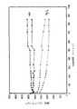
図3は、デバイスに対する印加電圧の関数としての輝度を示すものである。
データから理解されるように、閾値電圧である145Vよりも60V高い電圧での輝度は、約180カンデラ/m2であった。
The device was subjected to a test by applying a 240 Hz AC square wave voltage waveform having a pulse width of 30 ns and 60 V higher than the optical threshold voltage.
FIG. 3 shows the luminance as a function of the applied voltage to the device.
As understood from the data, the luminance at a voltage 60V higher than the threshold voltage 145V was about 180 candela / m 2 .
(実施例2)
デバイスは、窒化アルミニウムの誘電体層を同様の厚さのアルミナ層に置き換えた以外は実施例1と同様に調製された。
このデバイスの輝度データも図3に示されており、閾値電圧である160Vよりも60V高い電圧で、約120カンデラ/m2の輝度を示した。
窒化アルミニウム層を有するデバイスのより低い閾値電圧の原因は、アルミナに比べて窒化アルミニウムが高い誘電率を有していることにある。
窒化アルミニウム層を有するデバイスに閾値電圧よりも60V高い電圧を印加した際の輝度は、アルミナ層を有するデバイスの輝度に比べて約40%高くなっている。
(Example 2)
The device was prepared as in Example 1, except that the aluminum nitride dielectric layer was replaced with an alumina layer of similar thickness.
The brightness data of this device is also shown in FIG. 3 and showed a brightness of about 120 candela / m 2 at a voltage 60V higher than the threshold voltage of 160V.
The cause of the lower threshold voltage of devices having an aluminum nitride layer is that aluminum nitride has a higher dielectric constant than alumina.
The luminance when a voltage 60V higher than the threshold voltage is applied to the device having the aluminum nitride layer is about 40% higher than the luminance of the device having the alumina layer.
(実施例3)
デバイスは、蛍光層を、ユーロピウムで活性化されたバリウム・チオアルミ酸塩に代えてスパッタリングによりテルビウムで活性化された硫化亜鉛とした以外は実施例1と同様に調製された。
同じ試験条件下でのデバイスに対する印加電圧の関数としての輝度が図4に示されている。
データから理解されるように、閾値電圧である170Vよりも60V高い電圧での輝度は、約3000カンデラ/m2であった。
(Example 3)
The device was prepared as in Example 1 except that the fluorescent layer was zinc sulfide activated with terbium by sputtering instead of barium thioaluminate activated with europium.
The brightness as a function of applied voltage for the device under the same test conditions is shown in FIG.
As understood from the data, the luminance at a voltage 60V higher than the threshold voltage of 170V was about 3000 candela / m 2 .
(実施例4)
デバイスは、窒化アルミニウムの誘電体層を同様の厚さのアルミナ層に置き換えた以外は実施例3と同様に調製された。
同じ試験条件下での、このデバイスについての輝度データも図4に示されており、閾値電圧である180Vよりも60V高い電圧での輝度は、約2100カンデラ/m2であった。
ユーロピウムで活性化されたバリウム・チオアルミ酸塩の蛍光物質を有するデバイスと同様に、この実施例のデバイスは、窒化アルミニウム層を有する実施例3のデバイスよりも高い閾値電圧を呈しており、再度言及すると、この原因は、アルミナに比べて窒化アルミニウムが高い誘電率を有していることにある。
窒化アルミニウム層を有するデバイスについて閾値電圧よりも60V高い電圧を印加した際の輝度は、アルミナ層を有するデバイスの対応する輝度に比べて約40%高くなっている。
Example 4
The device was prepared as in Example 3, except that the aluminum nitride dielectric layer was replaced with an alumina layer of similar thickness.
The luminance data for this device under the same test conditions is also shown in FIG. 4 and the luminance at a voltage 60V higher than the threshold voltage of 180V was about 2100 candela / m 2 .
Similar to the device with the europium activated barium thioaluminate phosphor, the device of this example exhibits a higher threshold voltage than the device of Example 3 with an aluminum nitride layer and is mentioned again. This is because aluminum nitride has a higher dielectric constant than alumina.
The luminance when a voltage 60V higher than the threshold voltage is applied to the device having the aluminum nitride layer is about 40% higher than the corresponding luminance of the device having the alumina layer.
(実施例5)
デバイスは、酸窒化アルミニウムを形成するために窒化アルミニウム層に酸素がドーピングされている以外は実施例3と同様に調製された。
図4に示されるように、閾値電圧及び輝度の値は、純窒化アルミニウムを有する場合の値と純アルミナを有する場合の値との間を示している。
(Example 5)
The device was prepared as in Example 3 except that the aluminum nitride layer was doped with oxygen to form aluminum oxynitride.
As shown in FIG. 4, the values of the threshold voltage and the luminance are between the values in the case of having pure aluminum nitride and the values in the case of having pure alumina.
(実施例6)
デバイスは、蛍光層を、ユーロピウムで活性化されたバリウム・チオアルミ酸塩に代えて、マンガンで活性化された860nmの厚さの硫化亜鉛とした以外は実施例1と同様に調製された。
同じ試験条件下での、このデバイスに対する印加電圧の関数としての輝度が図5に示されている。
データから理解されるように、閾値電圧である150Vよりも60V高い電圧での輝度は、約4000カンデラ/m2であった。
(Example 6)
The device was prepared as in Example 1 except that the fluorescent layer was replaced with europium activated barium thioaluminate instead of manganese activated 860 nm thick zinc sulfide.
The brightness as a function of applied voltage for this device under the same test conditions is shown in FIG.
As understood from the data, the luminance at a voltage 60 V higher than the threshold voltage of 150 V was about 4000 candela / m 2 .
(実施例7)
デバイスは、窒化アルミニウムの誘電体層を同様の厚さのアルミナ層に置き換えた以外は実施例6と同様に調製された。
同じ試験条件下での、このデバイスについての輝度データも図5に示されており、閾値電圧である160Vよりも60V高い電圧での輝度は、約3700カンデラ/m2であった。
ユーロピウムで活性化されたバリウム・チオアルミ酸塩の蛍光物質を有するデバイスと同様に、この実施例のデバイスは、窒化アルミニウム層を有する実施例3のデバイスよりも高い閾値電圧を呈しているものの、これらの実施例での差異は小さくなっている。
窒化アルミニウム層を有するデバイスについて閾値電圧よりも60V高い電圧を印加した際の輝度は、アルミナ層を有するデバイスの対応する輝度に比べて約10%高くなっている。
(Example 7)
The device was prepared as in Example 6, except that the aluminum nitride dielectric layer was replaced with a similarly thick alumina layer.
The luminance data for this device under the same test conditions is also shown in FIG. 5 and the luminance at a voltage 60V higher than the threshold voltage of 160V was about 3700 candela / m 2 .
Similar to the device with the europium activated barium thioaluminate phosphor, the device of this example exhibits a higher threshold voltage than the device of Example 3 with an aluminum nitride layer. The difference in the embodiment is small.
The brightness when a voltage 60V higher than the threshold voltage is applied to the device having the aluminum nitride layer is about 10% higher than the corresponding brightness of the device having the alumina layer.
(実施例8)
実施例1及び実施例2のデバイスと同様な2つのデバイスを作製し、同一の駆動条件下で耐久テストに供した。
図6は、窒化アルミニウムの上部誘電体層とアルミナの上部誘電体層を有するエレクトロルミネッセンスデバイスについての比較耐久データを示すものであって、この図から、チオアルミ酸塩蛍光膜の上に蒸着された窒化アルミニウム膜は、該チオアルミ酸塩蛍光物質を安定化させる効果を有していることがわかる。
このデータによると、アルミナの上部誘電体層を有するデバイスについては200時間後に輝度がゼロにまで低下してしまうが、窒化アルミニウムの上部誘電体層を有するデバイスについては、初期の落ち込み期間の後はずっと緩やかに輝度が現象していくことが理解される。
(Example 8)
Two devices similar to those of Example 1 and Example 2 were manufactured and subjected to an endurance test under the same driving conditions.
FIG. 6 shows comparative durability data for an electroluminescent device having an upper dielectric layer of aluminum nitride and an upper dielectric layer of alumina, from which the vapor deposited on the thioaluminate phosphor film. It can be seen that the aluminum nitride film has the effect of stabilizing the thioaluminate phosphor.
According to this data, for devices with an alumina top dielectric layer, the brightness drops to zero after 200 hours, but for devices with an aluminum nitride top dielectric layer, after the initial drop period, It can be seen that the brightness phenomenon occurs much more slowly.
(実施例9)
テルビウムで活性化された硫化亜鉛の蛍光物質を有する4つのデバイスであって、そのうち2つは窒化アルミニウムの上部誘電体層を有する実施例3と同様に調製し、他の2つはアルミナの上部誘電体層を有する実施例4と同様に調製し、これら4つのデバイスを同一の駆動条件下で駆動周波数600Hzにて耐久テストに供した。
図7は、窒化アルミニウムの上部誘電体層とアルミナの上部誘電体層を有するエレクトロルミネッセンスデバイスについての比較耐久データを示すものであって、この図から、窒化アルミニウム膜は、硫化亜鉛の蛍光物質を安定化させる効果を有していることがわかる。
このデータによると、前者のデバイスの初期輝度は約2700カンデラ/m2であって、850時間作動後も実質的な変化は生じなかった。
これに対して後者のデバイスは前者と同様の初期輝度を示していたが、最初に約2200カンデラ/m2まで急激に落ち込んだ後も緩やかな輝度の低下を生じ、850時間の試験後には輝度は1500カンデラ/m2付近にまで低下した。
Example 9
Four devices with zinc sulfide phosphors activated with terbium, two of which were prepared as in Example 3 with an upper dielectric layer of aluminum nitride, the other two being the top of alumina Prepared in the same manner as in Example 4 having a dielectric layer, these four devices were subjected to a durability test at a driving frequency of 600 Hz under the same driving conditions.
FIG. 7 shows comparative durability data for an electroluminescent device having an upper dielectric layer of aluminum nitride and an upper dielectric layer of alumina. From this figure, the aluminum nitride film is made of a zinc sulfide phosphor. It turns out that it has the effect of stabilizing.
According to this data, the initial luminance of the former device was about 2700 candela / m 2 , and there was no substantial change after 850 hours of operation.
On the other hand, the latter device showed the same initial luminance as the former, but after the first sudden drop to about 2200 candela / m 2, a gradual decrease in luminance occurred, and after 850 hours of testing, the luminance decreased. Decreased to around 1500 candela / m 2 .
本発明の好適な実施形態が本明細書に詳細に説明されているけれども、当業者が、本発明の精神、または添付クレームの技術的範囲を逸脱することなくこれら実施形態に種々の変形を為し得ることが理解されるであろう。 While preferred embodiments of the present invention have been described in detail herein, those skilled in the art may make various modifications to these embodiments without departing from the spirit of the invention or the scope of the appended claims. It will be understood that this is possible.
10 デバイス
12 基板
14 金属導体層
16 厚膜誘電体層
18 平滑層
20 バリア層
22 蛍光層
24 薄膜誘電体層
26 ITO移動電極
28 密閉筐体
10
Claims (31)
(a)希土類で活性化されたバリウム・チオアルミ酸塩、
(b)希土類で活性化された微粒状の硫化亜鉛、
(c)遷移金属で活性化された硫化亜鉛、
(d)希土類または遷移金属で活性化されたセレン化亜鉛、及び
(e)希土類または遷移金属で活性化されたスルホセレン化亜鉛
から成る一群から選択され、
前記(a)、(b)、(d)及び(e)の蛍光膜には、該蛍光膜の上面及び/または下面に窒化アルミニウムのバリア層が設けられ、
前記(c)の蛍光膜には、該蛍光膜の側面上に窒化アルミニウムのバリア層が設けられ、
該窒化アルミニウムのバリア層は、前記蛍光膜と前記ディスプレイとの間の界面の安定性を向上させている、
ことを特徴とする蛍光膜。 An improved phosphor film for thick film dielectric electroluminescent displays, the phosphor film comprising:
(A) barium thioaluminate activated with rare earth,
(B) a particulate zinc sulfide activated with a rare earth;
(C) zinc sulfide activated with a transition metal,
Selected from the group consisting of (d) zinc selenide activated with a rare earth or transition metal, and (e) zinc sulfoselenide activated with a rare earth or transition metal,
The fluorescent films (a), (b), (d) and (e) are provided with an aluminum nitride barrier layer on the upper surface and / or lower surface of the fluorescent film,
The fluorescent film of (c) is provided with an aluminum nitride barrier layer on the side surface of the fluorescent film,
The aluminum nitride barrier layer improves the stability of the interface between the phosphor film and the display.
A fluorescent film characterized by that.
AはMg、Ca、Sr及びBaから成る群の一以上から選択され、
BはAl、Ga及びInから成る群の一以上から選択され、
CはS及びSeから成る群の一以上から選択される、
ことを特徴とする請求項1に記載の蛍光膜。 The barium thioaluminate phosphor film is represented by the chemical formula AB x C y : RE,
A is selected from one or more of the group consisting of Mg, Ca, Sr and Ba;
B is selected from one or more of the group consisting of Al, Ga and In;
C is selected from one or more of the group consisting of S and Se,
The phosphor film according to claim 1.
REはテルビウム及びユーロピウムから成る群から選択されると共に、前記蛍光物質が約50nmに至る結晶粒寸法を有していることを特徴とする請求項1に記載の蛍光物質。 The fine-grained zinc sulfide phosphor layer activated with rare earth is represented by the chemical formula ZnS: RE,
The phosphor of claim 1, wherein RE is selected from the group consisting of terbium and europium, and wherein the phosphor has a grain size of up to about 50 nm.
Aが活性化元素であることを特徴とする請求項1に記載の蛍光物質。 The zinc sulfoselenide is represented by the chemical formula ZnS x Se 1-x : A (0 <x <1),
The fluorescent substance according to claim 1, wherein A is an activating element.
Aが活性化元素であることを特徴とする請求項1に記載の蛍光物質。 The phosphor material of zinc selenide is represented by the chemical formula ZnSe: A,
The fluorescent substance according to claim 1, wherein A is an activating element.
Aはマンガン及びテルビウムから選択されることを特徴とする請求項1に記載の蛍光物質。 The zinc sulfide activated with a transition metal is represented by the chemical formula ZnS: A,
The fluorescent substance according to claim 1, wherein A is selected from manganese and terbium.
(a)希土類で活性化されたバリウム・チオアルミ酸塩、
(b)希土類で活性化された微粒状の硫化亜鉛、
(c)遷移金属で活性化された硫化亜鉛、
(d)希土類または遷移金属で活性化されたセレン化亜鉛、及び
(e)希土類または遷移金属で活性化されたスルホセレン化亜鉛
から成る一群から選択される蛍光物質薄膜層を有しており、
前記(a)、(b)、(d)及び(e)の蛍光層にあっては、該蛍光層の上面及び/または下面に直接的に隣接して設けられ、前記(c)の蛍光層にあっては、該蛍光層の上面に直接的に隣接して設けられる窒化アルミニウム層を備えていることを特徴とする積層体。 A laminate of phosphors used in a thick film dielectric electroluminescent display, the laminate comprising:
(A) barium thioaluminate activated with rare earth,
(B) a particulate zinc sulfide activated with a rare earth;
(C) zinc sulfide activated with a transition metal,
A phosphor thin film layer selected from the group consisting of (d) zinc selenide activated with a rare earth or transition metal, and (e) zinc sulfoselenide activated with a rare earth or transition metal,
The fluorescent layers (a), (b), (d) and (e) are provided directly adjacent to the upper surface and / or the lower surface of the fluorescent layer, and the fluorescent layer (c) In this case, the laminate includes an aluminum nitride layer provided directly adjacent to the upper surface of the fluorescent layer.
(a)希土類で活性化されたバリウム・チオアルミ酸塩、
(b)希土類で活性化された微粒状の硫化亜鉛、
(c)遷移金属で活性化された硫化亜鉛、
(d)希土類または遷移金属で活性化されたセレン化亜鉛、及び
(e)希土類または遷移金属で活性化されたスルホセレン化亜鉛
から成る一群から選択される蛍光物質を有しており、
前記(a)、(b)、(d)及び(e)の蛍光膜にあっては、前記蛍光膜とデバイスの残余の部分との間の界面の安定性を向上させるために前記蛍光膜の上面及び/または下面に窒化アルミニウムのバリア層を形成し、
前記(c)の蛍光膜にあっては、該蛍光層の上面側に窒化アルミニウムのバリア層を形成していること、
を特徴とするデバイス。 A thick film dielectric electroluminescent device configured on a glass substrate or a glass ceramic substrate, the device comprising:
(A) barium thioaluminate activated with rare earth,
(B) a particulate zinc sulfide activated with a rare earth;
(C) zinc sulfide activated with a transition metal,
Having a fluorescent material selected from the group consisting of (d) zinc selenide activated with a rare earth or transition metal, and (e) zinc sulfoselenide activated with a rare earth or transition metal,
In the fluorescent films (a), (b), (d), and (e), the fluorescent film is used in order to improve the stability of the interface between the fluorescent film and the rest of the device. Forming an aluminum nitride barrier layer on the upper and / or lower surface;
In the phosphor film of (c), an aluminum nitride barrier layer is formed on the upper surface side of the phosphor layer,
Device characterized by.
i) (a)希土類で活性化されたバリウム・チオアルミ酸塩、
(b)希土類で活性化された微粒状の硫化亜鉛、
(c)遷移金属で活性化された硫化亜鉛、
(d)希土類または遷移金属で活性化されたセレン化亜鉛、及び
(e)希土類または遷移金属で活性化されたスルホセレン化亜鉛
から成る一群から選択される蛍光物質を、第一のセットのアドレスラインと誘電体層とを組み込んだガラス基板またはガラスセラミック基板上に蒸着するステップと、
ii) 前記(a)〜(e)の蛍光膜の上に窒化アルミニウムの層を蒸着するステップと、
iii) 前記蛍光膜を約1100℃に至る温度で焼鈍するステップと、
を備えていることを特徴とする方法。 A method for making a stabilized phosphor stack for use in a thick film dielectric electroluminescent device comprising:
i) (a) rare earth activated barium thioaluminate,
(B) a particulate zinc sulfide activated with a rare earth;
(C) zinc sulfide activated with a transition metal,
A phosphor selected from the group consisting of (d) rare earth or transition metal activated zinc selenide, and (e) rare earth or transition metal activated zinc selenide, a first set of address lines And vapor deposition on a glass substrate or glass ceramic substrate incorporating the dielectric layer;
ii) depositing an aluminum nitride layer on the phosphor films of (a) to (e);
iii) annealing the phosphor film at a temperature up to about 1100 ° C .;
A method characterized by comprising:
28. The method of claim 27, comprising depositing the aluminum nitride barrier layer by atomic layer vapor deposition.
Applications Claiming Priority (2)
| Application Number | Priority Date | Filing Date | Title |
|---|---|---|---|
| US43463902P | 2002-12-20 | 2002-12-20 | |
| PCT/CA2003/001892 WO2004057925A1 (en) | 2002-12-20 | 2003-12-05 | Aluminum nitride passivated phosphors for electroluminescent displays |
Publications (1)
| Publication Number | Publication Date |
|---|---|
| JP2006511046A true JP2006511046A (en) | 2006-03-30 |
Family
ID=32682080
Family Applications (1)
| Application Number | Title | Priority Date | Filing Date |
|---|---|---|---|
| JP2004560943A Pending JP2006511046A (en) | 2002-12-20 | 2003-12-05 | Phosphors passivated with aluminum nitride for electroluminescent displays |
Country Status (10)
| Country | Link |
|---|---|
| US (1) | US7442446B2 (en) |
| EP (1) | EP1574114B1 (en) |
| JP (1) | JP2006511046A (en) |
| KR (1) | KR20050089971A (en) |
| CN (1) | CN1820551B (en) |
| AT (1) | ATE406081T1 (en) |
| AU (1) | AU2003287820A1 (en) |
| CA (1) | CA2509417A1 (en) |
| DE (1) | DE60323145D1 (en) |
| WO (1) | WO2004057925A1 (en) |
Families Citing this family (13)
| Publication number | Priority date | Publication date | Assignee | Title |
|---|---|---|---|---|
| JP2005536606A (en) * | 2002-08-29 | 2005-12-02 | アイファイア テクノロジー コーポレーション | Particulate rare earth activated zinc sulfide phosphor for electroluminescent display |
| US10340424B2 (en) | 2002-08-30 | 2019-07-02 | GE Lighting Solutions, LLC | Light emitting diode component |
| US7800121B2 (en) | 2002-08-30 | 2010-09-21 | Lumination Llc | Light emitting diode component |
| JP2004265740A (en) * | 2003-02-28 | 2004-09-24 | Tdk Corp | El functional film and el element |
| US7812522B2 (en) | 2004-07-22 | 2010-10-12 | Ifire Ip Corporation | Aluminum oxide and aluminum oxynitride layers for use with phosphors for electroluminescent displays |
| US20060181192A1 (en) * | 2004-08-02 | 2006-08-17 | Gelcore | White LEDs with tailorable color temperature |
| EP1875779A4 (en) * | 2005-04-15 | 2009-11-25 | Ifire Ip Corp | BARRIER LAYER CONTAINING MAGNESIUM OXIDE FOR THICK DIELECTRIC ELECTROLUMINESCENT DISPLAYS |
| WO2008131531A1 (en) * | 2007-04-30 | 2008-11-06 | Ifire Ip Corporation | Laminated thick film dielectric structure for thick film dielectric electroluminescent displays |
| US8456082B2 (en) * | 2008-12-01 | 2013-06-04 | Ifire Ip Corporation | Surface-emission light source with uniform illumination |
| US8158200B2 (en) | 2009-08-18 | 2012-04-17 | University Of North Texas | Methods of forming graphene/(multilayer) boron nitride for electronic device applications |
| US8593040B2 (en) | 2009-10-02 | 2013-11-26 | Ge Lighting Solutions Llc | LED lamp with surface area enhancing fins |
| US9500355B2 (en) | 2012-05-04 | 2016-11-22 | GE Lighting Solutions, LLC | Lamp with light emitting elements surrounding active cooling device |
| CN114695749A (en) * | 2020-12-31 | 2022-07-01 | Tcl科技集团股份有限公司 | Optoelectronic device |
Family Cites Families (43)
| Publication number | Priority date | Publication date | Assignee | Title |
|---|---|---|---|---|
| US4188565A (en) * | 1977-09-16 | 1980-02-12 | Sharp Kabushiki Kaisha | Oxygen atom containing film for a thin-film electroluminescent element |
| US4721631A (en) * | 1985-02-14 | 1988-01-26 | Sharp Kabushiki Kaisha | Method of manufacturing thin-film electroluminescent display panel |
| GB2195823B (en) * | 1986-09-29 | 1990-01-10 | Ricoh Kk | Thin film electroluminescent device |
| JPH088147B2 (en) | 1987-07-10 | 1996-01-29 | 松下電器産業株式会社 | Thin film EL device |
| JPH01232695A (en) * | 1988-03-11 | 1989-09-18 | Matsushita Electric Ind Co Ltd | Thin film electroluminescent element |
| US4975338A (en) * | 1988-04-12 | 1990-12-04 | Ricoh Company, Ltd. | Thin film electroluminescence device |
| JPH02103893A (en) * | 1988-04-12 | 1990-04-16 | Ricoh Co Ltd | Thin film electroluminescence device |
| JPH02103894A (en) * | 1988-04-13 | 1990-04-16 | Ricoh Co Ltd | Thin film electroluminescent device |
| US5372839A (en) * | 1988-05-13 | 1994-12-13 | Sharp Kabushiki Kaisha | Process for preparing an electroluminescent film |
| US4897319A (en) * | 1988-07-19 | 1990-01-30 | Planar Systems, Inc. | TFEL device having multiple layer insulators |
| JPH0322392A (en) * | 1989-06-20 | 1991-01-30 | Matsushita Electric Ind Co Ltd | Thin film el element |
| JPH04264392A (en) * | 1991-02-19 | 1992-09-21 | Clarion Co Ltd | Electroluminescence element |
| US5432015A (en) * | 1992-05-08 | 1995-07-11 | Westaim Technologies, Inc. | Electroluminescent laminate with thick film dielectric |
| FI92897C (en) | 1993-07-20 | 1995-01-10 | Planar International Oy Ltd | Process for producing a layer structure for electroluminescence components |
| US5505986A (en) * | 1994-02-14 | 1996-04-09 | Planar Systems, Inc. | Multi-source reactive deposition process for the preparation of blue light emitting phosphor layers for AC TFEL devices |
| US5598059A (en) * | 1994-04-28 | 1997-01-28 | Planar Systems, Inc. | AC TFEL device having a white light emitting multilayer phosphor |
| JP3561549B2 (en) | 1995-04-07 | 2004-09-02 | 三洋電機株式会社 | Organic electroluminescence device |
| JP2803631B2 (en) * | 1995-07-03 | 1998-09-24 | 株式会社デンソー | ELECTROLUMINESCENT ELEMENT AND ITS MANUFACTURING METHOD |
| US5644190A (en) * | 1995-07-05 | 1997-07-01 | Advanced Vision Technologies, Inc. | Direct electron injection field-emission display device |
| JPH1017395A (en) * | 1996-07-02 | 1998-01-20 | Hitachi Ltd | Multilayer thin film with controlled orientation and method of manufacturing the same |
| JPH1092580A (en) | 1996-09-19 | 1998-04-10 | Fuji Electric Co Ltd | Thin-film electroluminescence device and method for manufacturing the same |
| JPH11195487A (en) * | 1997-12-27 | 1999-07-21 | Tdk Corp | Organic EL device |
| US6064150A (en) * | 1998-01-12 | 2000-05-16 | Osram Sylvania Inc. | Nitride coated particle and composition of matter comprised of such particles |
| US6254806B1 (en) * | 1998-07-17 | 2001-07-03 | Bruker Ax, Inc. | High efficiency polycrystalline phosphors and method of making same |
| US6146225A (en) * | 1998-07-30 | 2000-11-14 | Agilent Technologies, Inc. | Transparent, flexible permeability barrier for organic electroluminescent devices |
| WO2000036665A1 (en) | 1998-12-16 | 2000-06-22 | Battelle Memorial Institute | Environmental barrier material for organic light emitting device and method of making |
| CN100382354C (en) * | 1999-02-15 | 2008-04-16 | 出光兴产株式会社 | Organic electroluminescence element and its manufacturing method |
| US6771019B1 (en) | 1999-05-14 | 2004-08-03 | Ifire Technology, Inc. | Electroluminescent laminate with patterned phosphor structure and thick film dielectric with improved dielectric properties |
| TW421862B (en) * | 1999-08-31 | 2001-02-11 | Ind Tech Res Inst | Packaging method of an organic electroluminescent display |
| US6353286B1 (en) * | 1999-10-08 | 2002-03-05 | Motorola, Inc | Field emission display having a multi-layered barrier structure |
| JP2002015872A (en) | 2000-06-29 | 2002-01-18 | Matsushita Electric Ind Co Ltd | EL element |
| JP3780182B2 (en) | 2000-07-18 | 2006-05-31 | キヤノン株式会社 | Image forming apparatus |
| EP1175000B1 (en) | 2000-07-19 | 2006-01-18 | STMicroelectronics S.r.l. | Start procedure for brushless motors |
| US6628077B2 (en) | 2000-10-27 | 2003-09-30 | Sony Corporation | Alternating current driven type plasma display |
| JP2002151270A (en) | 2000-11-07 | 2002-05-24 | Matsushita Electric Ind Co Ltd | EL lamp |
| TW522577B (en) | 2000-11-10 | 2003-03-01 | Semiconductor Energy Lab | Light emitting device |
| US6803122B2 (en) | 2000-12-12 | 2004-10-12 | Tdk Corporation | EL device |
| US6610352B2 (en) | 2000-12-22 | 2003-08-26 | Ifire Technology, Inc. | Multiple source deposition process |
| US6589674B2 (en) | 2001-01-17 | 2003-07-08 | Ifire Technology Inc. | Insertion layer for thick film electroluminescent displays |
| US20020125821A1 (en) * | 2001-03-12 | 2002-09-12 | University Of Cincinnati | Electroluminescent display formed on glass with a thick film dielectric layer |
| US6617782B2 (en) * | 2001-05-30 | 2003-09-09 | Ifire Technology Inc. | Thioaluminate phosphor material with a gadolinium co-activator |
| JP3704068B2 (en) * | 2001-07-27 | 2005-10-05 | ザ ウエステイム コーポレイション | EL panel |
| US7812522B2 (en) * | 2004-07-22 | 2010-10-12 | Ifire Ip Corporation | Aluminum oxide and aluminum oxynitride layers for use with phosphors for electroluminescent displays |
-
2003
- 2003-12-05 CA CA002509417A patent/CA2509417A1/en not_active Abandoned
- 2003-12-05 EP EP03779617A patent/EP1574114B1/en not_active Expired - Lifetime
- 2003-12-05 WO PCT/CA2003/001892 patent/WO2004057925A1/en not_active Ceased
- 2003-12-05 DE DE60323145T patent/DE60323145D1/en not_active Expired - Fee Related
- 2003-12-05 AT AT03779617T patent/ATE406081T1/en not_active IP Right Cessation
- 2003-12-05 JP JP2004560943A patent/JP2006511046A/en active Pending
- 2003-12-05 KR KR1020057011325A patent/KR20050089971A/en not_active Ceased
- 2003-12-05 AU AU2003287820A patent/AU2003287820A1/en not_active Abandoned
- 2003-12-05 CN CN2003801068942A patent/CN1820551B/en not_active Expired - Fee Related
- 2003-12-15 US US10/736,020 patent/US7442446B2/en not_active Expired - Fee Related
Also Published As
| Publication number | Publication date |
|---|---|
| EP1574114A1 (en) | 2005-09-14 |
| WO2004057925A1 (en) | 2004-07-08 |
| US20040170864A1 (en) | 2004-09-02 |
| EP1574114B1 (en) | 2008-08-20 |
| KR20050089971A (en) | 2005-09-09 |
| CN1820551A (en) | 2006-08-16 |
| CA2509417A1 (en) | 2004-07-08 |
| AU2003287820A1 (en) | 2004-07-14 |
| US7442446B2 (en) | 2008-10-28 |
| ATE406081T1 (en) | 2008-09-15 |
| CN1820551B (en) | 2010-10-06 |
| DE60323145D1 (en) | 2008-10-02 |
Similar Documents
| Publication | Publication Date | Title |
|---|---|---|
| JP5073148B2 (en) | Magnesium barium thioaluminate and similar phosphor materials | |
| CN100484354C (en) | Insertion layer for thick film electroluminescent displays | |
| JP2006511046A (en) | Phosphors passivated with aluminum nitride for electroluminescent displays | |
| US7129633B2 (en) | Silicon oxynitride passivated rare earth activated thioaluminate phosphors for electroluminescent displays | |
| US7812522B2 (en) | Aluminum oxide and aluminum oxynitride layers for use with phosphors for electroluminescent displays | |
| US7534504B2 (en) | Fine-grained rare earth activated zinc sulfide phosphors for electroluminescent displays | |
| JP5355076B2 (en) | Magnesium oxide-containing barrier layer for dielectric thick film electroluminescent displays | |
| JP2005538516A (en) | Thin film phosphor for electroluminescence display |
Legal Events
| Date | Code | Title | Description |
|---|---|---|---|
| A621 | Written request for application examination |
Free format text: JAPANESE INTERMEDIATE CODE: A621 Effective date: 20061130 |
|
| A711 | Notification of change in applicant |
Free format text: JAPANESE INTERMEDIATE CODE: A711 Effective date: 20090114 |
|
| A131 | Notification of reasons for refusal |
Free format text: JAPANESE INTERMEDIATE CODE: A131 Effective date: 20090804 |
|
| A02 | Decision of refusal |
Free format text: JAPANESE INTERMEDIATE CODE: A02 Effective date: 20100105 |