JP2006216196A - Nonvolatile semiconductor memory device - Google Patents
Nonvolatile semiconductor memory device Download PDFInfo
- Publication number
- JP2006216196A JP2006216196A JP2005030364A JP2005030364A JP2006216196A JP 2006216196 A JP2006216196 A JP 2006216196A JP 2005030364 A JP2005030364 A JP 2005030364A JP 2005030364 A JP2005030364 A JP 2005030364A JP 2006216196 A JP2006216196 A JP 2006216196A
- Authority
- JP
- Japan
- Prior art keywords
- voltage
- memory cell
- ref
- iref
- channel mos
- Prior art date
- Legal status (The legal status is an assumption and is not a legal conclusion. Google has not performed a legal analysis and makes no representation as to the accuracy of the status listed.)
- Withdrawn
Links
Images


Landscapes
- Tests Of Electronic Circuits (AREA)
- Read Only Memory (AREA)
- For Increasing The Reliability Of Semiconductor Memories (AREA)
Abstract
Description
この発明は、不揮発性半導体記憶装置に関し、特に、リファレンスメモリセルを用いて、ノーマルメモリセルに記憶されたデータを読出す不揮発性半導体記憶装置に関する。 The present invention relates to a nonvolatile semiconductor memory device, and more particularly to a nonvolatile semiconductor memory device that uses a reference memory cell to read data stored in a normal memory cell.
電気的にデータ書込およびデータ消去が可能な不揮発性メモリの代表例として、フラッシュメモリが適用されている。 A flash memory is applied as a typical example of a nonvolatile memory capable of electrically writing and erasing data.
図12は、フラッシュメモリのメモリセル構造を示す概念図である。図12を参照して、フラッシュメモリのメモリセルMCは、P型基板101上に形成されるNウェル102と、Nウェル102上に形成されるPウェル103と、Pウェル103上に形成されるn+領域であるソース104およびドレイン105を含む。メモリセルMCは、さらに、フローティングゲート106およびコントロールゲート107を含む。フローティングゲート106およびコントロールゲート107は、絶縁膜108によって絶縁されて、Pウェル103上に積層される。特に、フローティングゲート106およびコントロールゲート107の間の絶縁膜をインターポリ絶縁膜108aとも称し、フローティングゲート106およびPウェル103の間の絶縁膜をトンネル絶縁膜108bとも称する。このメモリセルMCはnチャネル電界効果型トランジスタに相当する。
FIG. 12 is a conceptual diagram showing the memory cell structure of the flash memory. Referring to FIG. 12, memory cell MC of the flash memory is formed on N well 102 formed on
コントロールゲート107は、メモリセルMCを選択するためのワード線WLと結合される。ソース104およびドレイン105は、それぞれソース線SLおよびビット線BLと結合される。
初期状態であるデータ消去状態においては、メモリセルMCにおいて、フローティングゲート106からエレクトロン109が引抜かれる。
In the data erase state, which is an initial state,
具体的には、メモリセルMCのコントロールゲート107およびソース104に、負電圧Vnnおよび高電圧Vppがそれぞれ印加される。これにより、メモリセルMCにおいて、フローティングゲート106からファウラーノルドヘイムトンネリング現象によってエレクトロン109が引抜かれて、データ消去が実行される。
Specifically, negative voltage Vnn and high voltage Vpp are applied to
これに対して、メモリセルMCに対するデータ書込は、フローティングゲート106に対するチャネルホットエレクトロン注入現象によるエレクトロン109の注入によって実行される。
On the other hand, data writing to the memory cell MC is executed by injection of
具体的には、ワード線WLおよびビット線BLを介して、ソース線SLに接地電圧Vssが印加された状態でコントロールゲート107およびドレイン105に高電圧Vppおよび所定電圧Vdwがそれぞれ印加された場合、チャネルホットエレクトロン注入現象によってエレクトロン109がフローティングゲート106に注入されて、データ書込が実行される。
Specifically, when the high voltage Vpp and the predetermined voltage Vdw are respectively applied to the
ここで、フローティングゲート106にエレクトロン109が注入された、すなわちデータ書込状態のメモリセルMCのしきい値電圧Vthは、データ消去状態よりも高くなる。したがって、最初に各メモリセルMCに対してデータ消去を実行し、その上で、選択的なデータ書込を実行することによって、データ書込を実行されたメモリセルのしきい値電圧のみが上昇することになる。
Here, the threshold voltage Vth of the memory cell MC in which
これにより、メモリセルMCにおけるしきい値電圧Vthの高/低に応じて、記憶データを読出すことができる。記憶データの読出は、予めビット線BLをプリチャージしておき、コントロールゲート107と結合されたワード線WLに一定電圧を与えてある所定時間ディスチャージを行なって、それからビット線BLの電位を検出することによって実行される。
Thereby, stored data can be read in accordance with the high / low threshold voltage Vth in memory cell MC. To read the stored data, the bit line BL is precharged in advance, a predetermined voltage is applied to the word line WL coupled to the
具体的には、データ読出時においては、ビット線BLは所定電圧Vdrにあらかじめプリチャージされる。また、ソース線SLは、接地電圧Vssが供給される。そして、ある所定時間の間、選択されたワード線WLに対してデータ読出のための所定電圧Vwrが印可される。これにより、対応するメモリセルMCのコントロールゲート107は、所定電圧Vwrに設定される。
Specifically, at the time of data reading, the bit line BL is precharged in advance to a predetermined voltage Vdr. The source line SL is supplied with the ground voltage Vss. Then, for a predetermined time, a predetermined voltage Vwr for data reading is applied to the selected word line WL. Thereby, the
これらの電圧Vwr、Vdrを、データ書込されたメモリセルMCのしきい値電圧Vthを考慮して適切に設定することによって、データ書込が実行されている場合においては、メモリセルMCがオン状態とならないためプリチャージされた電荷は保存される。その一方で、データ書込が実行されていない場合においてはメモリセルMCがオン状態となるため、プリチャージされた電荷は、メモリセルMCを介してソース線SLに放電されビット線BLの電位は、ディスチャージされ下がる。したがって、その後、ビット線BLに残っている電荷量を検出することによって、データ読出が可能である。 By appropriately setting these voltages Vwr and Vdr in consideration of the threshold voltage Vth of the memory cell MC to which data has been written, the memory cell MC is turned on when data writing is being executed. Since it is not in a state, the precharged charge is stored. On the other hand, since memory cell MC is turned on when data writing is not executed, the precharged charge is discharged to source line SL through memory cell MC, and the potential of bit line BL is , Discharged and lowered. Therefore, thereafter, data can be read by detecting the amount of charge remaining on the bit line BL.
このようにして、フローティングゲート106に対するエレクトロン109の注入の有/無に応じて、各メモリセルMCに対して不揮発的なデータ書込を実行するとともに、その記憶データを読出すことが可能である。
In this way, it is possible to execute nonvolatile data writing to each memory cell MC and read the stored data in accordance with the presence / absence of injection of
近年では、フラッシュメモリの低コスト化および大容量化を実現するために、各メモリセルにおいて複数のデータを書込可能な、いわゆる多値技術が用いられる。たとえば4値のNOR型フラッシュメモリにおいては、1つのメモリセルに対して、2ビットのデータ(“11”“10”“01”“00”)が記憶される。 In recent years, a so-called multi-value technique capable of writing a plurality of data in each memory cell is used in order to reduce the cost and increase the capacity of a flash memory. For example, in a quaternary NOR type flash memory, 2-bit data (“11” “10” “01” “00”) is stored for one memory cell.
図13は、4値のフラッシュメモリにおけるメモリセルのしきい値電圧分布を示す概念図である。図13を参照して、4値のフラッシュメモリにおいては、データ“11”に相当するデータ消去状態L0のほかに、3つのデータ書込状態L1、L2およびL3が定義される。たとえば、データ書込状態L1、L2およびL3は、データ“10”、“01”および“00”にそれぞれ相当する。 FIG. 13 is a conceptual diagram showing a threshold voltage distribution of memory cells in a quaternary flash memory. Referring to FIG. 13, in the quaternary flash memory, three data write states L1, L2 and L3 are defined in addition to a data erase state L0 corresponding to data “11”. For example, data write states L1, L2, and L3 correspond to data “10”, “01”, and “00”, respectively.
データ書込時における印加電圧レベル(高電圧Vpp)等のデータ書込条件を適切に設定することにより、データ書込状態L1〜L3におけるしきい値電圧の分布はそれぞれ異なるものとなる。データ書込状態L1〜L3の各々に対応したしきい値電圧の分布状態の境界に、データ読出レベルVtr1〜Vtr3は設定される。 By appropriately setting data writing conditions such as an applied voltage level (high voltage Vpp) at the time of data writing, the threshold voltage distributions in the data writing states L1 to L3 are different from each other. Data read levels Vtr1 to Vtr3 are set at boundaries between threshold voltage distribution states corresponding to data write states L1 to L3, respectively.
ここで、メモリセルのしきい値電圧が高くなるほどメモリセルに流れるセル電流は小さくなる。データ消去時は、ファウラーノルドヘイムトンネリング現象を利用して、メモリセルのしきい値電圧が高い状態から低い状態になるように、すなわちセル電流が小さな状態から大きな状態になるように、消去パルスを印加する。具体的には、セル電流値がデータ消去状態L0の基準電流値IREF_EVよりも大きくなるまで、消去パルスを印加する。 Here, the higher the threshold voltage of the memory cell, the smaller the cell current flowing through the memory cell. When erasing data, using the Fowler-Nordheim tunneling phenomenon, an erase pulse is applied so that the threshold voltage of the memory cell changes from a high state to a low state, that is, from a small state to a large state. Apply. Specifically, the erase pulse is applied until the cell current value becomes larger than the reference current value IREF_EV in the data erase state L0.
データ書込時は、チャネルホットエレクトロン注入現象を利用して、メモリセルのしきい値電圧が低い状態から高い状態になるように、すなわちセル電流が大きな状態から小さな状態になるように、書込パルスを印加する。具体的には、セル電流値がデータ書込状態L1〜L3の各々の基準電流値IREF_PV1,IREF_PV2,IREF_PV3よりも小さくなるまで、書込パルスを印加する。 When writing data, the channel hot electron injection phenomenon is used so that the threshold voltage of the memory cell is changed from a low state to a high state, that is, the cell current is changed from a large state to a small state. Apply a pulse. Specifically, the write pulse is applied until the cell current value becomes smaller than the respective reference current values IREF_PV1, IREF_PV2, and IREF_PV3 in the data write states L1 to L3.
データ読出時は、しきい値電圧のデータ読出レベルVtr1〜Vtr3の各々に対応した基準電流値IREF_R1,IREF_R2,IREF_R3に応じて、記憶データが読み分けられる。具体的には、セル電流値が基準電流値IREF_R1よりも大きい場合は、データ消去状態L0(“11”)であると判定される。セル電流値が基準電流値IREF_R1よりも小さく、基準電流値IREF_R2よりも大きい場合は、データ書込状態L1(“10”)であると判定される。セル電流値が基準電流値IREF_R2よりも小さく、基準電流値IREF_R3よりも大きい場合は、データ書込状態L2(“01”)であると判定される。セル電流値が基準電流値IREF_R3よりも小さい場合は、データ書込状態L3(“00”)であると判定される。 At the time of data reading, the stored data is read according to the reference current values IREF_R1, IREF_R2, and IREF_R3 corresponding to the data reading levels Vtr1 to Vtr3 of the threshold voltage. Specifically, when the cell current value is larger than the reference current value IREF_R1, it is determined that the data erase state L0 (“11”). When the cell current value is smaller than the reference current value IREF_R1 and larger than the reference current value IREF_R2, it is determined that the data write state L1 (“10”). When the cell current value is smaller than the reference current value IREF_R2 and larger than the reference current value IREF_R3, the data write state L2 (“01”) is determined. When the cell current value is smaller than the reference current value IREF_R3, it is determined that the data write state L3 (“00”).
このように、4値のフラッシュメモリでは、セル電流の大きさに基づいてメモリセルの4つの状態L0〜L3を定義している。通常、データ消去、データ書込およびデータ読出を行なうノーマルメモリセルMC_NORと同一形状のリファレンスメモリセルMC_REFを設け、このリファレンスメモリセルMC_REFに流れるセル電流を基準電流とする。リファレンスメモリセルMC_REFのしきい値電圧を制御して、基準電流値IREF_R1,IREF_R2,IREF_R3,IREF_EV,IREF_PV1,IREF_PV2,IREF_PV3を予め設定する。そして、これらの基準電流値IREF_R1,IREF_R2,IREF_R3,IREF_EV,IREF_PV1,IREF_PV2,IREF_PV3を用いて、ノーマルメモリセルのデータ消去、データ書込およびデータ読出を行なう。 As described above, in the four-value flash memory, the four states L0 to L3 of the memory cell are defined based on the magnitude of the cell current. Usually, a reference memory cell MC_REF having the same shape as that of a normal memory cell MC_NOR that performs data erasing, data writing, and data reading is provided, and a cell current flowing through the reference memory cell MC_REF is used as a reference current. Reference current values IREF_R1, IREF_R2, IREF_R3, IREF_EV, IREF_PV1, IREF_PV2, and IREF_PV3 are preset by controlling the threshold voltage of the reference memory cell MC_REF. Then, using these reference current values IREF_R1, IREF_R2, IREF_R3, IREF_EV, IREF_PV1, IREF_PV2, and IREF_PV3, data erasure, data writing and data reading of normal memory cells are performed.
リードマージンが大きく、動作の信頼性の高いフラッシュメモリを実現するためには、メモリセルの電気的特性を高精度にモニタする必要がある。リファレンスメモリセルMC_REFの電流−電圧特性を高精度に測定することによって、基準電流値IREF_R1,IREF_R2,IREF_R3,IREF_EV,IREF_PV1,IREF_PV2,IREF_PV3を高精度に調整することが可能になる。そして、高精度に調整された基準電流値IREF_R1,IREF_R2,IREF_R3,IREF_EV,IREF_PV1,IREF_PV2,IREF_PV3を用いて、ノーマルメモリセルMC_NORのデータ消去、データ書込およびデータ読出を正確に行なうことが可能になる。また、ノーマルメモリセルMC_NORの電流−電圧特性を高精度に測定することによって、不良セルを解析することが可能になる。 In order to realize a flash memory with a large read margin and high operation reliability, it is necessary to monitor the electrical characteristics of the memory cell with high accuracy. By measuring the current-voltage characteristics of the reference memory cell MC_REF with high accuracy, the reference current values IREF_R1, IREF_R2, IREF_R3, IREF_EV, IREF_PV1, IREF_PV2, and IREF_PV3 can be adjusted with high accuracy. Then, it is possible to accurately perform data erasure, data writing and data reading of the normal memory cell MC_NOR using the reference current values IREF_R1, IREF_R2, IREF_R3, IREF_EV, IREF_PV1, IREF_PV2 and IREF_PV3 adjusted with high accuracy. Become. In addition, it is possible to analyze a defective cell by measuring the current-voltage characteristics of the normal memory cell MC_NOR with high accuracy.
従来は、内部で生成した基準電流IVRSAの値を変更しながら、センスアンプを用いてセル電流値と基準電流IVRSAの値とを比較し、センスアンプの出力信号のレベルが反転するときの基準電流IVRSAの値が、セル電流値であると判定していた。しかし、内部で生成する基準電流IVRSAのばらつき、およびセンスアンプのオフセット特性のばらつきに起因して、正確なセル電流値が得られないことがあった。 Conventionally, the reference current when the level of the output signal of the sense amplifier is inverted by comparing the cell current value with the value of the reference current IVRSA using the sense amplifier while changing the value of the internally generated reference current IVRSA. The value of IVRSA was determined to be the cell current value. However, accurate cell current values may not be obtained due to variations in internally generated reference current IVRSA and variations in sense amplifier offset characteristics.
下記の特許文献1には、メモリセルの電気的特性を直接測定でき、歩留り、不良品解析の精度を向上させることができる不揮発性半導体記憶装置が開示されている。この場合、外部端子と各メモリセルアレイとをそれぞれ接続する複数のスイッチング素子と、このスイッチング素子をそれぞれ選択してオンし、同一ビット列のメモリセルアレイ上の特定のメモリセルから外部端子までの電流経路を形成する同一ビット列選択手段とを設け、外部端子に任意の電圧を供給することにより電流経路を介して特定のメモリセルの素子に電流を流すようにしている。
上述のように、従来の不揮発性半導体記憶装置では、内部で生成する基準電流IVRSAのばらつき、およびセンスアンプのオフセット特性のばらつきに起因して、正確なセル電流値が得られないことがあった。メモリセルの電気的特性の測定精度がよくないと、基準電流値IREF_R1,IREF_R2,IREF_R3,IREF_EV,IREF_PV1,IREF_PV2,IREF_PV3を正確に設定することができない。このため、リードマージンが小さくなり、フラッシュメモリの動作の信頼性が低くなっていた。 As described above, in the conventional nonvolatile semiconductor memory device, an accurate cell current value may not be obtained due to variations in the internally generated reference current IVRSA and variations in the offset characteristics of the sense amplifier. . If the measurement accuracy of the electrical characteristics of the memory cell is not good, the reference current values IREF_R1, IREF_R2, IREF_R3, IREF_EV, IREF_PV1, IREF_PV2, and IREF_PV3 cannot be set accurately. For this reason, the read margin is reduced and the operation reliability of the flash memory is lowered.
また、上記の特許文献1に開示された方法では、外部端子からメモリセルの電気的特性を直接測定できるという特徴を有するが、外部端子と各メモリセルアレイとをそれぞれ接続する複数のスイッチング素子の占有面積が大きかった。 In addition, the method disclosed in Patent Document 1 has a feature that the electrical characteristics of the memory cell can be directly measured from the external terminal. However, the method occupies a plurality of switching elements respectively connecting the external terminal and each memory cell array. The area was large.
それゆえに、この発明の主たる目的は、メモリセルの電気的特性を高精度に測定することが可能な小面積の不揮発性半導体記憶装置を提供することである。 Therefore, a main object of the present invention is to provide a nonvolatile semiconductor memory device having a small area capable of measuring the electrical characteristics of memory cells with high accuracy.
この発明に係わる不揮発性半導体記憶装置は、しきい値電圧のレベルに応じたデータを記憶するノーマルメモリセルと、しきい値電圧が予め定められたリファレンスメモリセルと、ノーマルメモリセルに流れる電流とリファレンスメモリセルに流れる電流とを比較して、ノーマルメモリセルに記憶されたデータを読出す読出回路と、外部端子と、第1の動作モード時にノーマルメモリセルにデータを書込むライトドライバと、第1の動作モード時にライトドライバを介して電源電圧を供給する電圧ノードとノーマルメモリセルとを接続し、第2の動作モード時にライトドライバを介して外部端子とリファレンスメモリセルとを接続する切換回路とを備えたものである。 A nonvolatile semiconductor memory device according to the present invention includes a normal memory cell for storing data corresponding to a threshold voltage level, a reference memory cell having a predetermined threshold voltage, and a current flowing through the normal memory cell. A read circuit for reading data stored in the normal memory cell by comparing the current flowing through the reference memory cell, an external terminal, a write driver for writing data to the normal memory cell in the first operation mode, A switching circuit for connecting a voltage node for supplying a power supply voltage via a write driver and a normal memory cell in the first operation mode and for connecting an external terminal and a reference memory cell via the write driver in the second operation mode; It is equipped with.
この発明に係わる他の不揮発性半導体記憶装置は、しきい値電圧のレベルに応じたデータを記憶するノーマルメモリセルと、しきい値電圧が予め定められたリファレンスメモリセルと、ノーマルメモリセルに流れる電流とリファレンスメモリセルに流れる電流とを比較して、ノーマルメモリセルに記憶されたデータを読出す読出回路と、外部端子と、第1の動作モード時にノーマルメモリセルにデータを書込むライトドライバと、第1の動作モード時にライトドライバを介して電源電圧を供給する電圧ノードとノーマルメモリセルとを接続し、第2の動作モード時にライトドライバを介して外部端子とノーマルメモリセルとを接続する切換回路とを備えたものである。 According to another nonvolatile semiconductor memory device of the present invention, a normal memory cell storing data corresponding to a threshold voltage level, a reference memory cell having a predetermined threshold voltage, and a normal memory cell flow A read circuit for comparing the current and the current flowing in the reference memory cell to read data stored in the normal memory cell; an external terminal; and a write driver for writing data to the normal memory cell in the first operation mode; Switching between connecting a voltage node for supplying a power supply voltage via a write driver and a normal memory cell in the first operation mode and connecting an external terminal and a normal memory cell via the write driver in the second operation mode And a circuit.
好ましくは、さらに、外部信号に応じて、ライトドライバの出力電圧のレベルを変化させる電圧制御部が設けられる。 Preferably, a voltage control unit is further provided for changing the level of the output voltage of the write driver in accordance with an external signal.
また好ましくは、ノーマルメモリセルは、しきい値電圧のレベルに応じた複数ビットのデータを記憶する。 Preferably, the normal memory cell stores a plurality of bits of data corresponding to the threshold voltage level.
この発明に係わる不揮発性半導体記憶装置では、しきい値電圧のレベルに応じたデータを記憶するノーマルメモリセルと、しきい値電圧が予め定められたリファレンスメモリセルと、ノーマルメモリセルに流れる電流とリファレンスメモリセルに流れる電流とを比較して、ノーマルメモリセルに記憶されたデータを読出す読出回路と、外部端子と、第1の動作モード時にノーマルメモリセルにデータを書込むライトドライバと、第1の動作モード時にライトドライバを介して電源電圧を供給する電圧ノードとノーマルメモリセルとを接続し、第2の動作モード時にライトドライバを介して外部端子とリファレンスメモリセルとを接続する切換回路とが設けられる。したがって、外部端子からライトドライバを介してリファレンスメモリセルのセル電流を直接測定することによって、リファレンスメモリセルの電気的特性を高精度に測定することができる。これにより、基準電流値を高精度に調整することが可能になる。したがって、リードマージンが大きく、動作の信頼性の高い不揮発性半導体記憶装置が実現できる。また、簡易な構成で実現されるため、面積ペナルティが非常に小さくてすむ。 In the nonvolatile semiconductor memory device according to the present invention, a normal memory cell for storing data corresponding to a threshold voltage level, a reference memory cell having a predetermined threshold voltage, and a current flowing through the normal memory cell A read circuit for reading data stored in the normal memory cell by comparing the current flowing through the reference memory cell, an external terminal, a write driver for writing data to the normal memory cell in the first operation mode, A switching circuit for connecting a voltage node for supplying a power supply voltage via a write driver and a normal memory cell in the first operation mode and for connecting an external terminal and a reference memory cell via the write driver in the second operation mode; Is provided. Therefore, the electrical characteristics of the reference memory cell can be measured with high accuracy by directly measuring the cell current of the reference memory cell from the external terminal via the write driver. This makes it possible to adjust the reference current value with high accuracy. Therefore, a nonvolatile semiconductor memory device having a large read margin and high operation reliability can be realized. In addition, since it is realized with a simple configuration, the area penalty is very small.
この発明に係わる他の不揮発性半導体記憶装置では、しきい値電圧のレベルに応じたデータを記憶するノーマルメモリセルと、しきい値電圧が予め定められたリファレンスメモリセルと、ノーマルメモリセルに流れる電流とリファレンスメモリセルに流れる電流とを比較して、ノーマルメモリセルに記憶されたデータを読出す読出回路と、外部端子と、第1の動作モード時にノーマルメモリセルにデータを書込むライトドライバと、第1の動作モード時にライトドライバを介して電源電圧を供給する電圧ノードとノーマルメモリセルとを接続し、第2の動作モード時にライトドライバを介して外部端子とノーマルメモリセルとを接続する切換回路とが設けられる。したがって、外部端子からライトドライバを介してノーマルメモリセルのセル電流を直接測定することによって、ノーマルメモリセルの電気的特性を高精度に測定することができる。これにより、不良セルを解析することが可能になる。また、簡易な構成で実現されるため、面積ペナルティが非常に小さくてすむ。 In another nonvolatile semiconductor memory device according to the present invention, a normal memory cell storing data corresponding to a threshold voltage level, a reference memory cell having a predetermined threshold voltage, and a normal memory cell flow A read circuit for comparing the current and the current flowing in the reference memory cell to read data stored in the normal memory cell; an external terminal; and a write driver for writing data to the normal memory cell in the first operation mode; Switching between connecting a voltage node for supplying a power supply voltage via a write driver and a normal memory cell in the first operation mode and connecting an external terminal and a normal memory cell via the write driver in the second operation mode A circuit is provided. Therefore, the electrical characteristics of the normal memory cell can be measured with high accuracy by directly measuring the cell current of the normal memory cell from the external terminal via the write driver. This makes it possible to analyze a defective cell. In addition, since it is realized with a simple configuration, the area penalty is very small.
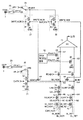
図1は、この発明の一実施の形態によるフラッシュメモリの全体構成図を示すブロック図である。図1において、このフラッシュメモリは、入力端子1,2と、外部端子3と、入出力端子4と、アドレスバッファ11と、制御回路12と、電圧発生回路13と、電圧分配回路14と、プリデコーダ15と、行デコーダ+レベルシフタ16と、列デコーダ+レベルシフタ17と、ワード線ドライバ18,19と、ノーマルメモリアレイ20とリファレンスメモリアレイ21と、列選択ゲート22,23と、センス制御回路24と、切換回路25,26,29,30と、書込回路27,28と、ライトドライバ31と、センスアンプ帯32と、データ制御回路33と、入出力バッファ34とを備える。
FIG. 1 is a block diagram showing an overall configuration diagram of a flash memory according to an embodiment of the present invention. In FIG. 1, this flash memory includes
アドレスバッファ11は、入力端子1からのアドレス信号をバッファリングして、制御回路12、プリデコーダ15およびセンス制御回路24に与える。制御回路12は、アドレスバッファ11からのアドレス信号を受けるとともに、入出力端子4からのコマンドを入出力バッファ34を介して受け、制御信号を出力する。電圧発生回路13は、制御回路12からの制御信号に応じて各種電圧を生成し、電圧分配回路14および切換回路30に与える。電圧分配回路14は、電圧発生回路13から受けた電圧を分配し、行デコーダ+レベルシフタ16、列デコーダ+レベルシフタ17および切換回路26に与える。
The
プリデコーダ15は、アドレスバッファ11からのアドレス信号を受け、行プリデコード信号および列プリデコード信号を出力する。行デコーダ+レベルシフタ16は、プリデコーダ15からの行プリデコード信号に応じて行選択信号を生成し、電圧分配回路14から与えられた電圧に応じて行選択信号を電圧変換する。列デコーダ+レベルシフタ17は、プリデコーダ15からの列プリデコード信号に応じて列選択信号を生成し、電圧分配回路14から与えられた電圧に応じて列選択信号を電圧変換する。
ワード線ドライバ18は、行デコーダ+レベルシフタ16からの行選択信号を受けて、ノーマルメモリアレイ20のワード線WL_NORを指定し、ワード線WL_NORに印可するパルス電圧振幅および印可時間を変化させる。ワード線ドライバ19は、行デコーダ+レベルシフタ16からの行選択信号を受けて、リファレンスメモリアレイ21のワード線WL_REFを指定し、ワード線WL_REFに印可するパルス電圧振幅および印可時間を変化させる。
The
ノーマルメモリアレイ20は、複数行複数列(たとえば256行2048列)に配置された複数のノーマルメモリセルMC_NORと、それぞれ複数行に対応して設けられた複数のワード線WL_NORと、それぞれ複数列に対応して設けられた複数のビット線BL_NORとを含む。リファレンスメモリアレイ21は、複数行複数列(たとえば3行96列)に配置された複数のリファレンスメモリセルMC_REFと、それぞれ複数行に対応して設けられた複数のワード線WL_REFと、それぞれ複数列に対応して設けられた複数のビット線BL_REFとを含む。リファレンスメモリセルMC_REFは、ノーマルメモリセルMC_NORと同一形状を有する。
なお、ノーマルメモリセルMC_NORおよびリファレンスメモリセルMC_REFは、たとえば図12に示したメモリセル構造を有し、4値のNOR型フラッシュメモリを構成する。ただし、NOR型フラッシュメモリに代わって、フローティングゲートを有さないメモリセル構造を有するNROM(Nitride Read Only Memory)としてもよい。このように、ノーマルメモリセルMC_NORおよびリファレンスメモリセルMC_REFは、そのしきい値電圧のレベルに応じた複数ビットのデータを記憶し、ノーマルメモリセルMC_NORとリファレンスメモリセルMC_REFに流れるセル電流を比較することによってデータ読出が行なわれるものとする。 The normal memory cell MC_NOR and the reference memory cell MC_REF have, for example, the memory cell structure shown in FIG. 12, and constitute a quaternary NOR type flash memory. However, an NROM (Nitride Read Only Memory) having a memory cell structure without a floating gate may be used instead of the NOR flash memory. As described above, the normal memory cell MC_NOR and the reference memory cell MC_REF store a plurality of bits of data corresponding to the threshold voltage level, and compare the cell currents flowing through the normal memory cell MC_NOR and the reference memory cell MC_REF. It is assumed that data reading is performed by.
列選択ゲート22は、列デコーダ+レベルシフタ17からの列選択信号によって指定されたビット線BL_NORとセンスアンプ帯32とを選択的に接続する。列選択ゲート23は、列デコーダ+レベルシフタ17からの列選択信号によって指定されたビット線BL_REFとセンスアンプ帯32とを選択的に接続する。
The
センス制御回路24は、アドレスバッファ11からのアドレス信号に応じて、ATD(Address Transition Detect)パルスを生成し、生成したATDパルスに応じてセンスアンプ帯32の読出動作を制御するための制御信号を出力する。
The sense control circuit 24 generates an ATD (Address Transition Detect) pulse according to the address signal from the
切換回路25は、オン/オフ制御され、入力端子2からの電圧EXWL(外部信号)を受け、電圧VPY2を出力する。切換回路26は、電圧分配回路14からの電圧VPY1および切換回路25からの電圧VPY2を受け、いずれか一方を選択して電圧VDWRTを出力する。
書込回路27は、切換回路26からの電圧VDWRTによって駆動され、電圧WRITE_NORを出力する。書込回路28は、切換回路26からの電圧VDWRTによって駆動され、電圧WRITE_REFを出力する。
Write
切換回路29は、オン/オフ制御され、外部端子3からの電圧XXLRPを受け、電圧VPP_ACCを出力する。切換回路30は、電圧発生回路13からの電圧VPLおよび切換回路29からの電圧VPP_ACCを受け、いずれか一方を選択して電源電圧VPDを出力する。ライトドライバ31は、切換回路30からの電源電圧VPDによって駆動され、電圧WDDATAを出力する。
The switching
センスアンプ帯32は、センス制御回路24からの制御信号、書込回路27,28からの電圧WRITE_NOR,WRITE_REFおよびライトドライバ31からの電圧WDDATAに応じて、指定されたメモリセルにデータ書込を行なう。または、指定されたメモリセルの記憶データを読出してデータ制御回路33に転送する。このセンスアンプ帯32は、複数列(たとえば32列)に配置されたセンスアンプを含む。
データ制御回路33は、センスアンプ帯32からのデータに適正な処理を行なって、入出力バッファ34に転送する。入出力バッファ34は、入出力端子4にデータを出力する。また、入出力端子4からのコマンドを制御回路12に与える。
The data control
図2は、図1に示したセンスアンプ帯32の1つの列の構成を詳細に示す回路ブロック図である。図2において、このセンスアンプ帯32の1つの列は、図1に示したノーマルメモリアレイ20の256行64列のノーマルメモリセルMC_NORおよびリファレンスメモリアレイ21の3行3列のリファレンスメモリセルMC_REFに対応して設けられる。
FIG. 2 is a circuit block diagram showing in detail the configuration of one column of
切換回路25の入力ノードは、入力端子2からの電圧EXWLを受ける。切換回路25の出力ノードからは電圧VPY2が出力される。切換回路26の第1および第2の入力ノードは、それぞれ電圧分配回路14からの電圧VPY1および切換回路25からの電圧VPY2を受ける。切換回路26の出力ノードからは電圧VPWRTが出力される。
An input node of switching
書込回路27は、切換回路26の出力ノードと接地電位GNDのラインとの間に直列接続されたPチャネルMOSトランジスタ51およびNチャネルMOSトランジスタ61を含む。PチャネルMOSトランジスタ51およびNチャネルMOSトランジスタ61のゲートは、ともに制御電圧IWRT_NORを受ける。
Write
書込回路28は、切換回路26の出力ノードと接地電位GNDのラインとの間に直列接続されたPチャネルMOSトランジスタ52およびNチャネルMOSトランジスタ62を含む。PチャネルMOSトランジスタ52およびNチャネルMOSトランジスタ62のゲートは、ともに制御電圧IWRT_REFを受ける。
Write
ライトドライバ31は、切換回路30の出力ノードと接地電位GNDのラインとの間に直列接続されたPチャネルMOSトランジスタ53およびNチャネルMOSトランジスタ63を含む。PチャネルMOSトランジスタ53およびNチャネルMOSトランジスタ63のゲートは、ともに制御電圧DATAを受ける。
Write
切換回路29の入力ノードは、外部端子3からの電圧XXLRPを受ける。切換回路29の出力ノードからは電圧VPP_ACCが出力される。切換回路30の第1および第2の入力ノードは、それぞれ切換回路29からの電圧VPP_ACCおよび電圧発生回路13からの電圧VPLを受ける。切換回路30の出力ノードからは電源電圧VPDが出力される。
An input node of switching
NチャネルMOSトランジスタ64は、PチャネルMOSトランジスタ53とNチャネルMOSトランジスタ63の間の出力ノードとノードN3との間に接続される。NチャネルMOSトランジスタ64のゲートは、書込回路27からの電圧WRITE_NORを受ける。
N
VRSA電圧発生回路42は、電圧VRSA_NORおよびVRSA_REFを生成する。NチャネルMOSトランジスタ65は、センスアンプ(SA)41の入力ノードN1と接地電位GNDのラインとの間に接続される。NチャネルMOSトランジスタ64のゲートは、VRSA電圧発生回路42からの電圧VRSA_NORを受ける。NチャネルMOSトランジスタ66は、センスアンプ41の入力ノードN2と接地電位GNDのラインとの間に接続される。NチャネルMOSトランジスタ66のゲートは、VRSA電圧発生回路42からの電圧VRSA_REFを受ける。
The VRSA
NチャネルMOSトランジスタ67は、センスアンプ41の入力ノードN1とノードN3との間に接続される。NチャネルMOSトランジスタ68は、センスアンプ41の入力ノードN2とノードN4との間に接続される。NチャネルMOSトランジスタ67,68のゲートは、ともに読出制御電圧READを受ける。
N
NチャネルMOSトランジスタ69は、ノードN3とノードN4との間に接続される。NチャネルMOSトランジスタ69のゲートは、書込回路28からの電圧WRITE_REFを受ける。ノードN3,N4の電圧は、それぞれBD_NOR,BD_REFである。
N
NチャネルMOSトランジスタ70,71は、ノードN3とノードN5との間に直列接続される。NチャネルMOSトランジスタ70,71のゲートは、それぞれ制御電圧CAU,CALを受ける。NチャネルMOSトランジスタ72は、ノードN4とノードN6との間に接続される。NチャネルMOSトランジスタ72のゲートは、制御電圧YG_REFを受ける。ノードN5,N6は、それぞれビット線BL_NOR,BL_REFに接続される。
N
ノードN5とノードN7との間には、NチャネルMOSトランジスタ73が設けられる。NチャネルMOSトランジスタ73のゲートは、制御電圧SG_NORを受ける。
An N
ノードN6とノードN8との間には、NチャネルMOSトランジスタ74が設けられる。NチャネルMOSトランジスタ74のゲートは、制御電圧SG_REFを受ける。
An N
ノーマルメモリセルMC_NORは、ノードN7とソース線SL_NORとの間に接続されたメモリトランジスタ75で構成される。メモリトランジスタ75のゲートは、ワード線WL_NORに接続される。リファレンスメモリセルMC_REFは、ノードN8とソース線SL_REFとの間に接続されたメモリトランジスタ76で構成される。メモリトランジスタ76のゲートは、ワード線WL_REFに接続される。ノードN7,N8の電圧は、それぞれVD_NOR,VD_REFである。
Normal memory cell MC_NOR is formed of a
なお、図示しないが、NチャネルMOSトランジスタ73およびノーマルメモリセルMC_NORは、それぞれ各ビット線BL_NORに対応して256行64列設けられる。すなわち、32列のセンスアンプ41に対応して、合計256行2048列設けられる。NチャネルMOSトランジスタ73は、制御電圧SG_NORに応じて、ノーマルメモリセルMC_NORを選択的にビット線BL_NORに接続する。
Although not shown, N
また、NチャネルMOSトランジスタ74およびリファレンスメモリセルMC_REFは、それぞれ各ビット線BL_REFに対応して3行3列設けられる。すなわち、32列のセンスアンプ41に対応して、合計3行96列設けられる。NチャネルMOSトランジスタ74は、制御電圧SG_REFに応じて、リファレンスメモリセルMC_REFを選択的にビット線BL_REFに接続する。
N
各ビット線BL_REFに対応して設けられる3行3列のリファレンスメモリセルMC_NORのうちの7つは、それぞれ基準電流値IREF_R1,IREF_R2,IREF_R3,IREF_EV,IREF_PV1,IREF_PV2,IREF_PV3が予め設定される。 Reference current values IREF_R1, IREF_R2, IREF_R3, IREF_EV, IREF_PV1, IREF_PV2, and IREF_PV3 are preset in seven of the three rows by three columns of reference memory cells MC_NOR provided corresponding to each bit line BL_REF.
NチャネルMOSトランジスタ70,71は図1に示した列選択ゲート22に配置され、NチャネルMOSトランジスタ72は図1に示した列選択ゲート23に配置される。また、NチャネルMOSトランジスタ73はノーマルメモリアレイ20に配置され、NチャネルMOSトランジスタ74はリファレンスメモリアレイ21に配置される。
N
ここで、ノーマルメモリセルMC_NORへのデータ書込動作について説明する。図2において、ノーマルメモリセルMC_NORへのデータ書込時の電流経路を点線矢印で示す。メモリセルへの書込動作は、チャネルホットエレクトロン注入現象を利用して行なわれる。 Here, a data write operation to normal memory cell MC_NOR will be described. In FIG. 2, a current path at the time of data writing to the normal memory cell MC_NOR is indicated by a dotted arrow. The write operation to the memory cell is performed using the channel hot electron injection phenomenon.
ノーマルメモリセルMC_NORへのデータ書込時において、切換回路25,29はともにオフ状態にされる。切換回路26は、入力電圧VPY1,VPY2のうち電圧VPY1を選択して出力する。切換回路30は、入力電圧VPP_ACC,VPLのうち電圧VPLを選択して出力する。
At the time of data writing to normal memory cell MC_NOR, both switching
図3は、各ノードの電圧値を示す図である。図2および図3を参照して、切換回路26は、出力電圧VPWRTを入力電圧VPY1と同じ8.5Vにする。書込回路27において、0Vの制御電圧IWRT_NORに応じて、PチャネルMOSトランジスタ51が導通し、NチャネルMOSトランジスタ61が非導通になる。このため、書込回路27の出力電圧WRITE_NORは、電圧VPWRTと同じ8.5Vにされる。書込回路28において、8.5Vの制御電圧IWRT_REFに応じて、PチャネルMOSトランジスタ52が非導通になり、NチャネルMOSトランジスタ62が導通する。このため、書込回路28の出力ノードの電圧WRITE_REFは、接地電圧0Vにされる。
FIG. 3 is a diagram illustrating the voltage value of each node. 2 and 3, switching
切換回路30は、出力電圧VPDを入力電圧VPLと同じ3.6Vにする。ライトドライバ31において、0Vの制御電圧DATAに応じて、PチャネルMOSトランジスタ53が導通し、NチャネルMOSトランジスタ63が非導通になる。このため、ライトドライバ31の出力電圧WDDATAは、電圧VPDと同じ3.6Vにされる。なお、図示しないが、ライトドライバ31は複数(たとえば64個)設けられ、選択されたメモリセルに対応するライトドライバの制御電圧DATAのみが0Vにされ、他のライトドライバの制御電圧DATAは3.6Vにされる。
The switching
NチャネルMOSトランジスタ65,66は、それぞれVRSA電圧発生回路42からの0Vの電圧VRSA_NOR,VRSA_REFに応じて非導通になる。NチャネルMOSトランジスタ67,68は、それぞれ0Vの読出制御電圧READに応じて非導通になる。このため、ノードN3,N4は、センスアンプ41と電気的に切離される。
N
NチャネルMOSトランジスタ64は、書込回路27からの8.5Vの電圧WRITE_NORに応じて導通する。このため、ノードN3の電圧BD_NORは、ライトドライバ31の出力電圧WDDATAと同じ3.6Vにされる。
N
NチャネルMOSトランジスタ69は、書込回路28からの0Vの電圧WRITE_REFに応じて非導通になる。また、NチャネルMOSトランジスタ72,74は、それぞれ0Vの制御電圧YG_REF,SG_REFに応じて非導通になる。このため、ノードN4の電圧BD_REFは0Vにされる。また、リファレンスメモリセルMC_REFは、ワード線WL_REFの電圧0Vに応じて非選択状態にされる。
N
NチャネルMOSトランジスタ70,71,73は、それぞれ8.5Vの制御電圧CAU,CAL,SG_NORに応じて導通する。したがって、ノーマルメモリセルMC_NORのドレイン(ノードN7)には、3.6Vの電圧VPLが切換回路30、PチャネルMOSトランジスタ53、NチャネルMOSトランジスタ64,70,71,73を介して印加される(印加電圧VD_NOR)。また、ノーマルメモリセルMC_NORのゲートには、ワード線WL_NORを介して2.5V〜8Vの書込パルスが印加される。このとき、ノーマルメモリセルMC_NORにはセル電流ICHE_NORが流れる。
N
図4は、ノーマルメモリセルMC_NORのゲートに印加される書込パルスを示す図である。図4において、3つのデータ書込状態L1〜L3(図13参照)の各々に対応して、データ書込が正常に完了するまでの間、書込パルスが複数ステップ印加される。この書込パルスの電圧値は、2.5Vから8Vまでの間で、繰返し印加されるごとに所定電圧ΔV1(たとえば、0.05V)ずつ上昇する。 FIG. 4 is a diagram showing a write pulse applied to the gate of normal memory cell MC_NOR. In FIG. 4, a write pulse is applied in a plurality of steps until data writing is normally completed corresponding to each of three data write states L1 to L3 (see FIG. 13). The voltage value of the write pulse rises by a predetermined voltage ΔV1 (for example, 0.05V) every time it is repeatedly applied between 2.5V and 8V.
各ステップの間では、メモリセルのしきい値電圧が所望の値まで上昇したか否か、すなわち、セル電流ICHE_NORが所望の値まで小さくなったか否かを判定するベリファイ動作を行なう。具体的には、3つのデータ書込状態L1〜L3の各々に対応して、セル電流ICHE_NORの値が基準電流値IREF_PV1〜IREF_PV3よりも小さくなったか否かを判定する。このベリファイ動作を行ないながら、セル電流ICHE_NORの値が所望の値よりも小さくなるまで書込パルスを印加し、所望の値よりも小さくなると書込パルスの印加を終了する。なお、図13を参照して、IREF_PV1>IREF_PV2>IREF_PV3の大小関係であるため、IREF_PV1に対応するしきい値電圧が最も低く、IREF_PV3に対応するしきい値電圧が最も高い。 Between each step, a verify operation is performed to determine whether or not the threshold voltage of the memory cell has increased to a desired value, that is, whether or not the cell current ICHE_NOR has decreased to a desired value. Specifically, it is determined whether or not the value of the cell current ICHE_NOR is smaller than the reference current values IREF_PV1 to IREF_PV3 corresponding to each of the three data write states L1 to L3. While performing this verify operation, the write pulse is applied until the value of the cell current ICHE_NOR becomes smaller than the desired value, and when the value becomes smaller than the desired value, the application of the write pulse is terminated. Referring to FIG. 13, since IREF_PV1> IREF_PV2> IREF_PV3, the threshold voltage corresponding to IREF_PV1 is the lowest and the threshold voltage corresponding to IREF_PV3 is the highest.
図5は、リファレンスメモリセルMC_REFへの書込動作について説明するための回路ブロック図である。図5において、リファレンスメモリセルMC_REFへの書込時の電流経路を点線矢印で示す。メモリセルへの書込動作は、チャネルホットエレクトロン注入現象を利用して行なわれる。 FIG. 5 is a circuit block diagram for describing a write operation to reference memory cell MC_REF. In FIG. 5, a current path at the time of writing to the reference memory cell MC_REF is indicated by a dotted arrow. The write operation to the memory cell is performed using the channel hot electron injection phenomenon.
リファレンスメモリセルMC_REFへの書込時において、切換回路25,29はともにオフ状態にされる。切換回路26は、入力電圧VPY1,VPY2のうち電圧VPY1を選択して出力する。切換回路30は、入力電圧VPP_ACC,VPLのうち電圧VPLを選択して出力する。
At the time of writing to the reference memory cell MC_REF, both the switching
図5および図3を参照して、切換回路26は、出力電圧VPWRTを入力電圧VPY1と同じ8.5Vにする。書込回路27において、0Vの制御電圧IWRT_NORに応じて、PチャネルMOSトランジスタ51が導通し、NチャネルMOSトランジスタ61が非導通になる。このため、書込回路27の出力電圧WRITE_NORは、電圧VPWRTと同じ8.5Vにされる。書込回路28において、0Vの制御電圧IWRT_REFに応じて、PチャネルMOSトランジスタ52が導通し、NチャネルMOSトランジスタ62が非導通になる。このため、書込回路28の出力ノードの電圧WRITE_REFは、電圧VPWRTと同じ8.5Vにされる。
5 and 3, switching
切換回路30は、出力電圧VPDを入力電圧VPLと同じ3.6Vにする。ライトドライバ31において、0Vの制御電圧DATAに応じて、PチャネルMOSトランジスタ53が導通し、NチャネルMOSトランジスタ63が非導通になる。このため、ライトドライバ31の出力電圧WDDATAは、電圧VPDと同じ3.6Vにされる。
The switching
NチャネルMOSトランジスタ65は、VRSA電圧発生回路42からの所定の電圧値Vαの電圧VRSA_NORに応じて導通する。NチャネルMOSトランジスタ66は、VRSA電圧発生回路42からの0Vの電圧VRSA_REFに応じて非導通になる。NチャネルMOSトランジスタ67,68は、それぞれ0Vの読出制御電圧READに応じて非導通になる。このため、ノードN3,N4は、センスアンプ41と電気的に切離される。
N-
NチャネルMOSトランジスタ67,68は、それぞれ0Vの読出制御電圧READに応じて非導通になる。このため、ノードN3,N4は、センスアンプ41と電気的に切離される。
N
NチャネルMOSトランジスタ64は、書込回路27からの8.5Vの電圧WRITE_NORに応じて導通する。このため、ノードN3の電圧BD_NORは、ライトドライバ31の出力電圧WDDATAと同じ3.6Vにされる。
N
NチャネルMOSトランジスタ69は、書込回路28からの8.5Vの電圧WRITE_REFに応じて導通する。これにより、ノードN4の電圧BD_REFはノードN3の電圧BD_NORと同じ3.6Vにされる。また、NチャネルMOSトランジスタ70,71,73は、それぞれ0Vの制御電圧CAU,CAL,SG_NORに応じて非導通になる。また、ノーマルメモリセルMC_NORは、ワード線WL_NORの電圧0Vに応じて非選択状態にされる。
N
NチャネルMOSトランジスタ72,74は、それぞれ8.5Vの制御電圧YG_REF,SG_REFに応じて導通する。したがって、リファレンスメモリセルMC_REFのドレイン(ノードN8)には、3.6Vの電圧VPLが切換回路30、PチャネルMOSトランジスタ53、NチャネルMOSトランジスタ64,69,72,74を介して印加される(印加電圧VD_REF)。また、リファレンスメモリセルMC_REFのゲートには、ワード線WL_REFを介して2.5V〜8Vの書込パルスが印加される。このとき、リファレンスメモリセルMC_REFにはセル電流ICHE_REFが流れる。
N
リファレンスメモリセルMC_REFのゲートには、図4に示した書込パルスと同様の書込パルスが印加される。具体的には、7つの基準電流値IREF_R1,IREF_R2,IREF_R3,IREF_EV,IREF_PV1,IREF_PV2,IREF_PV3(図13参照)の各々に対応して、書込動作が正常に完了するまでの間、書込パルスが複数ステップ印加される。この書込パルスの電圧値は、2.5Vから8Vまでの間で、繰返し印加されるごとに所定電圧ΔV1(たとえば、0.05V)ずつ上昇する。 A write pulse similar to the write pulse shown in FIG. 4 is applied to the gate of the reference memory cell MC_REF. Specifically, the write pulse corresponding to each of the seven reference current values IREF_R1, IREF_R2, IREF_R3, IREF_EV, IREF_PV1, IREF_PV2, and IREF_PV3 (see FIG. 13) until the write operation is normally completed. Are applied in multiple steps. The voltage value of the write pulse rises by a predetermined voltage ΔV1 (for example, 0.05V) every time it is repeatedly applied between 2.5V and 8V.
ここで、7つの基準電流値IREF_R1,IREF_R2,IREF_R3,IREF_EV,IREF_PV1,IREF_PV2,IREF_PV3を設定する際に、所望の基準電流値が得られているか否かを判定するベリファイ動作を行なう。このとき、読出制御電圧READが活性化レベルにされ、NチャネルMOSトランジスタ67,68がともに導通する。そして、VRSA電圧発生回路42からNチャネルMOSトランジスタ65のゲートに与える電圧VRSA_NORの値Vαを変化させることによって、NチャネルMOSトランジスタ65に流れる基準電流IVRSA_NORの値を変更する。基準電流IVRSA_NORの値を変更しながら、センスアンプ41を用いて、リファレンスメモリセルMC_REFに流れるセル電流ICHE_REFの値と基準電流IVRSA_NORの値とを比較して、センスアンプ41の出力信号のレベルが反転するときの基準電流IVRSA_NORの値が、リファレンスメモリセルMC_REFのセル電流値であると判定する。
Here, when seven reference current values IREF_R1, IREF_R2, IREF_R3, IREF_EV, IREF_PV1, IREF_PV2, and IREF_PV3 are set, a verify operation is performed to determine whether or not a desired reference current value is obtained. At this time, read control voltage READ is activated, and N
図6は、データ読出動作について説明するための回路ブロック図である。図6において、データ読出時の電流経路を点線矢印で示す。 FIG. 6 is a circuit block diagram for explaining the data read operation. In FIG. 6, the current path at the time of data reading is indicated by a dotted arrow.
データ読出時においては、読出制御電圧READが活性化レベルにされ、NチャネルMOSトランジスタ67,68がともに導通する。そして、センスアンプ41によって、ノーマルメモリセルMC_NORのセル電流INORとリファレンスメモリセルMC_REFの基準電流IREFとが比較され、ノーマルセルMC_NORの記憶データが読み分けられる。具体的には、ノーマルメモリセルMC_NORのセル電流値が基準電流値IREF_R1よりも大きい場合は、データ消去状態L0(“11”)であると判定される。ノーマルメモリセルMC_NORのセル電流値が基準電流値IREF_R1よりも小さく、基準電流値IREF_R2よりも大きい場合は、データ書込状態L1(“10”)であると判定される。ノーマルメモリセルMC_NORのセル電流値が基準電流値IREF_R2よりも小さく、基準電流値IREF_R3よりも大きい場合は、データ書込状態L2(“01”)であると判定される。ノーマルメモリセルMC_NORのセル電流値が基準電流値IREF_R3よりも小さい場合は、データ書込状態L3(“00”)であると判定される。
At the time of data reading, read control voltage READ is activated and N
ここで、リードマージンが大きく、動作の信頼性の高いフラッシュメモリを実現するためには、メモリセルの電気的特性を高精度にモニタする必要がある。 Here, in order to realize a flash memory with a large read margin and high operation reliability, it is necessary to monitor the electrical characteristics of the memory cell with high accuracy.
図7は、リファレンスメモリセルMC_REFの電流−電圧特性を測定する方法について説明するための回路ブロック図である。図7において、リファレンスメモリセルMC_REFのテスト時における電流経路を点線矢印で示す。 FIG. 7 is a circuit block diagram for explaining a method for measuring the current-voltage characteristics of the reference memory cell MC_REF. In FIG. 7, the current path during the test of the reference memory cell MC_REF is indicated by a dotted arrow.
リファレンスメモリセルMC_REFのテスト時において、切換回路25,29はともにオン状態にされる。切換回路26は、入力電圧VPY1,VPY2のうち電圧VPY2を選択して出力する。切換回路30は、入力電圧VPP_ACC,VPLのうち電圧VPP_ACCを選択して出力する。
At the time of testing the reference memory cell MC_REF, both the switching
図7および図3を参照して、切換回路25は、出力電圧VPY2を入力電圧EXWLと同じ2.0Vにする。切換回路26は、出力電圧VPWRTを入力電圧VPY2と同じ2.0Vにする。書込回路27において、0Vの制御電圧IWRT_NORに応じて、PチャネルMOSトランジスタ51が導通し、NチャネルMOSトランジスタ61が非導通になる。このため、書込回路27の出力電圧WRITE_NORは、電圧VPWRTと同じ2.0Vにされる。書込回路28において、0Vの制御電圧IWRT_REFに応じて、PチャネルMOSトランジスタ52が導通し、NチャネルMOSトランジスタ62が非導通になる。このため、書込回路28の出力ノードの電圧WRITE_REFは、電圧VPWRTと同じ2.0Vにされる。
7 and 3, switching
切換回路29は、出力電圧VPP_ACCを入力電圧XXLRPと同じ2.5Vにする。切換回路30は、出力電圧VPDを入力電圧VPP_ACCと同じ2.5Vにする。ライトドライバ31において、0Vの制御電圧DATAに応じて、PチャネルMOSトランジスタ53が導通し、NチャネルMOSトランジスタ63が非導通になる。このため、ライトドライバ31の出力電圧WDDATAは、電圧VPDと同じ2.5Vにされる。
The switching
NチャネルMOSトランジスタ65,66は、それぞれVRSA電圧発生回路42からの0Vの電圧VRSA_NOR,VRSA_REFに応じて非導通になる。NチャネルMOSトランジスタ67,68は、それぞれ0Vの読出制御電圧READに応じて非導通になる。このため、ノードN3,N4は、センスアンプ41と電気的に切離される。
N
NチャネルMOSトランジスタ64は、書込回路27からの2.0Vの電圧WRITE_NORに応じて導通する。ただし、ノードN3の電圧BD_NORは、ライトドライバ31の出力電圧WDDATA(2.5V)からNチャネルMOSトランジスタ64による電圧降下を伴って0.9Vにされる。
N
NチャネルMOSトランジスタ69は、書込回路28からの2.0Vの電圧WRITE_REFに応じて導通する。これにより、ノードN4の電圧BD_REFはノードN3の電圧BD_NORと同じ0.9Vにされる。また、NチャネルMOSトランジスタ70,71,73は、それぞれ0Vの制御電圧CAU,CAL,SG_NORに応じて非導通になる。また、ノーマルメモリセルMC_NORは、ワード線WL_NORの電圧0Vに応じて非選択状態にされる。
N
NチャネルMOSトランジスタ72は、5.0Vの制御電圧YG_REFに応じて導通する。NチャネルMOSトランジスタ74は、5.5Vの制御電圧SG_REFに応じて導通する。したがって、リファレンスメモリセルMC_REFのドレイン(ノードN8)には、2.5Vの電圧XXLRPが切換回路29,30、PチャネルMOSトランジスタ53、NチャネルMOSトランジスタ64,69,72,74を介して、電圧降下を伴って印加される(印加電圧VD_REF)。また、リファレンスメモリセルMC_REFのゲートには、ワード線WL_REFを介して5.5Vの電圧が印加される。このように、メモリセルを1つずつ選択して電流−電圧特性を測定する。
N
なお、入力端子2、切換回路25,26、書込回路27,28およびNチャネルMOSトランジスタ64,69は電圧制御部を構成し、外部から入力端子2に与えられる電圧EXWL(外部信号)に応じて、ライトドライバ31の出力電圧のレベルを変化させる。すなわち、入力端子2に与えられる電圧EXWLに応じて、電圧WRITE_NOR,WRITE_REFのレベルが変化し、リファレンスメモリセルMC_REFのドレイン電圧VD_REFが変化する。したがって、ドレイン電圧VD_REFを変化させながらセル電流IREFを測定することによって、セル電流IREFのドレイン電圧VD_REFに対する依存性を評価することができる。
図8は、リファレンスメモリセルMC_REFのセル電流IREFとドレイン電圧VD_REFとの関係を示す図である。図8において、ドレイン電圧VD_REFが高くなるほど、セル電流IREFは大きくなり、かつ電流−電圧特性曲線の傾きは小さくなる。ドレイン電圧VD_REFが小さい範囲では、電流−電圧特性曲線の傾きが大きく、セル電流IREFはドレイン電圧VD_REFに比例して増加する。この電流−電圧特性の領域を線形領域という。ドレイン電圧VD_REFが所定値V11を超えると、電流−電圧特性曲線の傾きが非常に小さくなり、セル電流IREFのドレイン電圧VD_REFに対する依存性が小さくなる。この電流−電圧特性の領域を飽和領域という。 FIG. 8 is a diagram showing the relationship between the cell current IREF and the drain voltage VD_REF of the reference memory cell MC_REF. In FIG. 8, as the drain voltage VD_REF increases, the cell current IREF increases and the slope of the current-voltage characteristic curve decreases. In the range where the drain voltage VD_REF is small, the slope of the current-voltage characteristic curve is large, and the cell current IREF increases in proportion to the drain voltage VD_REF. This region of current-voltage characteristics is called a linear region. When the drain voltage VD_REF exceeds the predetermined value V11, the slope of the current-voltage characteristic curve becomes very small, and the dependency of the cell current IREF on the drain voltage VD_REF becomes small. This region of current-voltage characteristics is called a saturation region.
リードマージンが大きく、動作の信頼性の高いフラッシュメモリを実現するためには、メモリセルを飽和領域で使用する必要がある。このため、セル電流IREFのドレイン電圧VD_REFに対する依存性を評価して、飽和領域になるドレイン電圧VD_REFの値V11を求める。そして、ドレイン電圧VD_REFが所定値V11よりも大きい範囲で、リファレンスメモリセルMC_REFを使用する。 In order to realize a flash memory with a large read margin and high operation reliability, it is necessary to use memory cells in a saturation region. For this reason, the dependency of the cell current IREF on the drain voltage VD_REF is evaluated to obtain the value V11 of the drain voltage VD_REF that becomes the saturation region. Then, the reference memory cell MC_REF is used in the range where the drain voltage VD_REF is larger than the predetermined value V11.
このように、この一実施の形態では、書込動作時に使用するライトドライバ31を利用して、リファレンスメモリセルMC_REFの電流−電圧特性を高精度に測定することができる。これにより、基準電流値IREF_R1,IREF_R2,IREF_R3,IREF_EV,IREF_PV1,IREF_PV2,IREF_PV3を高精度に調整することが可能になる。そして、高精度に調整された基準電流値IREF_R1,IREF_R2,IREF_R3,IREF_EV,IREF_PV1,IREF_PV2,IREF_PV3を用いて、ノーマルメモリセルのデータ消去、データ書込およびデータ読出を正確に行なうことが可能になる。
As described above, in this embodiment, the current-voltage characteristic of the reference memory cell MC_REF can be measured with high accuracy by using the
なお、外部端子3は、フラッシュメモリの消費電力を低下させ、リセット状態(またはスタンバイ状態)にするためのリセットパワーダウンピンである。このリセットパワーダウンピンは、ウェハ工程、組立て工程、検査工程、製品出荷後のいずれにおいても使用可能である。したがって、いずれの工程においてもメモリセルの電流−電圧特性を測定することができる。
The
図9は、ノーマルメモリセルMC_NORの電流−電圧特性を測定する方法について説明するための回路ブロック図である。図9において、ノーマルメモリセルMC_NORのテスト時における電流経路を点線矢印で示す。 FIG. 9 is a circuit block diagram for explaining a method of measuring current-voltage characteristics of normal memory cell MC_NOR. In FIG. 9, the current path during the test of the normal memory cell MC_NOR is indicated by a dotted arrow.
ノーマルメモリセルMC_NORのテスト時において、切換回路25,29はともにオン状態にされる。切換回路26は、入力電圧VPY1,VPY2のうち電圧VPY2を選択して出力する。切換回路30は、入力電圧VPP_ACC,VPLのうち電圧VPP_ACCを選択して出力する。
During the test of normal memory cell MC_NOR, both switching
図9および図3を参照して、切換回路25は、出力電圧VPY2を入力電圧EXWLと同じ2.0Vにする。切換回路26は、出力電圧VPWRTを入力電圧VPY2と同じ2.0Vにする。書込回路27において、0Vの制御電圧IWRT_NORに応じて、PチャネルMOSトランジスタ51が導通し、NチャネルMOSトランジスタ61が非導通になる。このため、書込回路27の出力電圧WRITE_NORは、電圧VPWRTと同じ2.0Vにされる。書込回路28において、2.0Vの制御電圧IWRT_REFに応じて、PチャネルMOSトランジスタ52が非導通になり、NチャネルMOSトランジスタ62が導通する。このため、書込回路28の出力ノードの電圧WRITE_REFは、接地電圧0Vにされる。
Referring to FIGS. 9 and 3, switching
切換回路29は、出力電圧VPP_ACCを入力電圧XXLRPと同じ2.5Vにする。切換回路30は、出力電圧VPDを入力電圧VPP_ACCと同じ2.5Vにする。ライトドライバ31において、0Vの制御電圧DATAに応じて、PチャネルMOSトランジスタ53が導通し、NチャネルMOSトランジスタ63が非導通になる。このため、ライトドライバ31の出力電圧WDDATAは、電圧VPDと同じ2.5Vにされる。
The switching
NチャネルMOSトランジスタ65,66は、それぞれVRSA電圧発生回路42からの0Vの電圧VRSA_NOR,VRSA_REFに応じて非導通になる。NチャネルMOSトランジスタ67,68は、それぞれ0Vの読出制御電圧READに応じて非導通になる。このため、ノードN3,N4は、センスアンプ41と電気的に切離される。
N
NチャネルMOSトランジスタ64は、書込回路27からの2.0Vの電圧WRITE_NORに応じて導通する。ただし、ノードN3の電圧BD_NORは、ライトドライバ31の出力電圧WDDATA(2.5V)からNチャネルMOSトランジスタ64による電圧降下を伴って0.9Vにされる。
N
NチャネルMOSトランジスタ69は、書込回路28からの0Vの電圧WRITE_REFに応じて非導通になる。また、NチャネルMOSトランジスタ72,74は、それぞれ0Vの制御電圧YG_REF,SG_REFに応じて非導通になる。このため、ノードN4の電圧BD_REFは0Vにされる。また、リファレンスメモリセルMC_REFは、ワード線WL_REFの電圧0Vに応じて非選択状態にされる。
N
NチャネルMOSトランジスタ70,71は、それぞれ5.0Vの制御電圧CAU,CALに応じて導通する。NチャネルMOSトランジスタ73は、5.5Vの制御電圧SGに応じて導通する。したがって、ノーマルメモリセルMC_NORのドレイン(ノードN7)には、2.5Vの電圧XXLRPが切換回路29,30、PチャネルMOSトランジスタ53、NチャネルMOSトランジスタ64,70,71,73を介して、電圧降下を伴って印加される(印加電圧VD_NOR)。また、ノーマルメモリセルMC_NORのゲートには、ワード線WL_NORを介して5.5Vの電圧が印加される。このように、メモリセルを1つずつ選択して電流−電圧特性を測定する。
N
なお、入力端子2、切換回路25,26、書込回路27,28およびNチャネルMOSトランジスタ64,69は電圧制御部を構成し、外部から入力端子2に与えられる電圧EXWL(外部信号)に応じて、ライトドライバ31の出力電圧のレベルを変化させる。すなわち、入力端子2に与えられる電圧EXWLに応じて、電圧WRITE_NORのレベルが変化し、ノーマルメモリセルMC_NORのドレイン電圧VD_NORが変化する。したがって、ドレイン電圧VD_NORを変化させながらセル電流INORを測定することによって、セル電流INORのドレイン電圧VD_NORに対する依存性を評価することができる。
ノーマルメモリセルMC_NORはリファレンスメモリセルMC_REFと同一形状であり、ノーマルメモリセルMC_NORのセル電流INORとドレイン電圧VD_NORとの関係は、図8に示したリファレンスメモリセルMC_REFのセル電流IREFとドレイン電圧VD_REFとの関係と同様である。 The normal memory cell MC_NOR has the same shape as the reference memory cell MC_REF, and the relationship between the cell current INOR and the drain voltage VD_NOR of the normal memory cell MC_NOR is the same as the cell current IREF and the drain voltage VD_REF of the reference memory cell MC_REF shown in FIG. It is the same as the relationship.
このように、この一実施の形態では、書込動作時に使用するライトドライバ31を利用して、ノーマルメモリセルMC_NORの電流−電圧特性を高精度に測定することができる。これにより、不良セルを解析することが可能になる。
As described above, in this embodiment, the current-voltage characteristic of the normal memory cell MC_NOR can be measured with high accuracy by using the
ここで、本発明によるメモリセルの電流−電圧特性の測定方法と対比して、従来の測定方法について説明する。 Here, a conventional measurement method will be described in contrast to the method for measuring current-voltage characteristics of a memory cell according to the present invention.
図10は、従来のリファレンスメモリセルMC_REFの電流−電圧特性の測定方法について説明するための回路ブロック図である。図10において、リファレンスメモリセルMC_REFのテスト時における電流経路を点線矢印で示す。 FIG. 10 is a circuit block diagram for explaining a method for measuring current-voltage characteristics of a conventional reference memory cell MC_REF. In FIG. 10, a current path at the time of testing the reference memory cell MC_REF is indicated by a dotted arrow.
リファレンスメモリセルMC_REFのテスト時において、切換回路25,29はともにオフ状態にされる。切換回路26は、入力電圧VPY1,VPY2のうち電圧VPY1を選択して出力する。切換回路30は、入力電圧VPP_ACC,VPLのうち電圧VPLを選択して出力する。
At the time of testing the reference memory cell MC_REF, both the switching
図10および図3を参照して、切換回路26は、出力電圧VPWRTを入力電圧VPY1と同じ5.0Vにする。書込回路27において、5.0Vの制御電圧IWRT_NORに応じて、PチャネルMOSトランジスタ51が非導通になり、NチャネルMOSトランジスタ61が導通する。このため、書込回路27の出力電圧WRITE_NORは、接地電圧0Vにされる。書込回路28において、5.0Vの制御電圧IWRT_REFに応じて、PチャネルMOSトランジスタ52が非導通になり、NチャネルMOSトランジスタ62が導通する。このため、書込回路28の出力ノードの電圧WRITE_REFは、接地電圧0Vにされる。
Referring to FIGS. 10 and 3, switching
切換回路30は、出力電圧VPDを入力電圧VPLと同じ3.6Vにする。ライトドライバ31において、3.6Vの制御電圧DATAに応じて、PチャネルMOSトランジスタ53が非導通になり、NチャネルMOSトランジスタ63が導通する。このため、ライトドライバ31の出力電圧WDDATAは、接地電圧0Vにされる。
The switching
NチャネルMOSトランジスタ64は、書込回路27からの0Vの電圧WRITE_NORに応じて非導通になる。このため、ライトドライバ31の出力ノードとノードN3とは電気的に切離される。NチャネルMOSトランジスタ69は、書込回路28からの0Vの電圧WRITE_REFに応じて非導通になる。これにより、ノードN3とノードN4とは電気的に切離される。
N
NチャネルMOSトランジスタ70,71,73は、それぞれ0Vの制御電圧CAU,CAL,SG_NORに応じて非導通になる。また、ノーマルメモリセルMC_NORは、ワード線WL_NORの電圧0Vに応じて非選択状態にされる。
N
NチャネルMOSトランジスタ67,68は、5.0Vの読出制御電圧READに応じて導通する。NチャネルMOSトランジスタ65は、VRSA電圧発生回路42からの所定の電圧値Vαの電圧VRSA_NORに応じて導通する。このNチャネルMOSトランジスタ65に流れる電流をIVRSA_NORとする。NチャネルMOSトランジスタ66は、VRSA電圧発生回路42からの0Vの電圧VRSA_REFに応じて非導通になる。
N
NチャネルMOSトランジスタ72は、5.0Vの制御電圧YG_REFに応じて導通する。NチャネルMOSトランジスタ74は、5.5Vの制御電圧SG_REFに応じて導通する。また、リファレンスメモリセルMC_REFのゲートには、ワード線WL_REFを介して5.5Vの電圧が印加される。
N
ここで、VRSA電圧発生回路42からNチャネルMOSトランジスタ65のゲートに与える電圧VRSA_NORの値Vαを変化させることによって、NチャネルMOSトランジスタ65に流れる基準電流IVRSA_NORの値を変更する。そして、基準電流IVRSA_NORの値を変更しながら、センスアンプ41を用いて、リファレンスメモリセルMC_REFに流れるセル電流IREFの値と基準電流IVRSA_NORの値とを比較して、センスアンプ41の出力信号のレベルが反転するときの基準電流IVRSA_NORの値が、リファレンスメモリセルMC_REFのセル電流値であると判定する。
Here, by changing the value Vα of the voltage VRSA_NOR given from the VRSA
しかし、このような従来の測定方法では、内部で生成する基準電流IVRSA_NORのばらつき、およびセンスアンプ41のオフセット特性のばらつきに起因して、正確なセル電流値が得られないことがあった。具体的には、NチャネルMOSトランジスタ65の特性(しきい値電圧など)のばらつきや、NチャネルMOSトランジスタ65のソースに与えられる接地電位GNDのばらつき(物理的な位置に依存したばらつき)に起因して、基準電流IVRSA_NORがばらつくことがある。また、センスアンプ固有の特性により、センスアンプ41の出力信号のレベルは、必ずしもセル電流IREFと基準電流IVRSA_NORとが等しくなった時に反転するわけではない。すなわち、セル電流IREF>基準電流IVRSA_NOR、またはセル電流IREF<基準電流IVRSA_NORであってもセンスアンプ41の出力信号のレベルが反転する場合がある。このように、センスアンプ毎にオフセット特性(カレントミラー回路の差動オフセット特性)がばらつくことがある。したがって、セル電流の測定値がばらつき、リファレンスメモリセルMC_REFの正確なセル電流値が得られないことがあった。
However, in such a conventional measurement method, an accurate cell current value may not be obtained due to variations in internally generated reference current IVRSA_NOR and variations in offset characteristics of the
図11は、従来のノーマルメモリセルMC_NORの電流−電圧特性の測定方法について説明するための回路ブロック図である。図11において、ノーマルメモリセルMC_NORのテスト時における電流経路を点線矢印で示す。 FIG. 11 is a circuit block diagram for explaining a method for measuring current-voltage characteristics of a conventional normal memory cell MC_NOR. In FIG. 11, a current path at the time of testing the normal memory cell MC_NOR is indicated by a dotted arrow.
ノーマルメモリセルMC_NORのテスト時において、切換回路25,29はともにオフ状態にされる。切換回路26は、入力電圧VPY1,VPY2のうち電圧VPY1を選択して出力する。切換回路30は、入力電圧VPP_ACC,VPLのうち電圧VPLを選択して出力する。
When testing normal memory cell MC_NOR, both switching
図11および図3を参照して、切換回路26は、出力電圧VPWRTを入力電圧VPY1と同じ5.0Vにする。書込回路27において、5.0Vの制御電圧IWRT_NORに応じて、PチャネルMOSトランジスタ51が非導通になり、NチャネルMOSトランジスタ61が導通する。このため、書込回路27の出力電圧WRITE_NORは、接地電圧0Vにされる。書込回路28において、5.0Vの制御電圧IWRT_REFに応じて、PチャネルMOSトランジスタ52が非導通になり、NチャネルMOSトランジスタ62が導通する。このため、書込回路28の出力ノードの電圧WRITE_REFは、接地電圧0Vにされる。
Referring to FIGS. 11 and 3, switching
切換回路30は、出力電圧VPDを入力電圧VPLと同じ3.6Vにする。ライトドライバ31において、3.6Vの制御電圧DATAに応じて、PチャネルMOSトランジスタ53が非導通になり、NチャネルMOSトランジスタ63が導通する。このため、ライトドライバ31の出力電圧WDDATAは、接地電圧0Vにされる。
The switching
NチャネルMOSトランジスタ64は、書込回路27からの0Vの電圧WRITE_NORに応じて非導通になる。このため、ライトドライバ31の出力ノードとノードN3とは電気的に切離される。NチャネルMOSトランジスタ69は、書込回路28からの0Vの電圧WRITE_REFに応じて非導通になる。これにより、ノードN3とノードN4とは電気的に切離される。
N
NチャネルMOSトランジスタ72,74は、それぞれ0Vの制御電圧YG_REF,SG_REFに応じて非導通になる。また、リファレンスメモリセルMC_REFは、ワード線WL_REFの電圧0Vに応じて非選択状態にされる。
N-
NチャネルMOSトランジスタ67,68は、5.0Vの読出制御電圧READに応じて導通する。NチャネルMOSトランジスタ65は、VRSA電圧発生回路42からの0Vの電圧VRSA_NORに応じて非導通になる。NチャネルMOSトランジスタ66は、VRSA電圧発生回路42からの所定の電圧値Vβの電圧VRSA_REFに応じて導通する。このNチャネルMOSトランジスタ66に流れる電流をIVRSA_REFとする。
N
NチャネルMOSトランジスタ70,71は、それぞれ5.0Vの制御電圧CAU,CALに応じて導通する。NチャネルMOSトランジスタ73は、5.5Vの制御電圧SG_NORに応じて導通する。また、ノーマルメモリセルMC_NORのゲートには、ワード線WL_NORを介して5.5Vの電圧が印加される。
N
ここで、VRSA電圧発生回路42からNチャネルMOSトランジスタ66のゲートに与える電圧VRSA_REFの値Vβを変化させることによって、NチャネルMOSトランジスタ66に流れる基準電流IVRSA_REFの値を変更する。そして、基準電流IVRSA_REFの値を変更しながら、センスアンプ41を用いて、ノーマルメモリセルMC_NORに流れるセル電流INORの値と基準電流IVRSA_REFの値とを比較して、センスアンプ41の出力信号のレベルが反転するときの基準電流IVRSA_REFの値が、ノーマルメモリセルMC_NORのセル電流値であると判定する。
Here, by changing the value Vβ of the voltage VRSA_REF applied from the VRSA
このような従来の測定方法では、内部で生成する基準電流IVRSA_REFのばらつき、およびセンスアンプ41のオフセット特性のばらつきに起因して、正確なセル電流値が得られないことがあった。具体的には、NチャネルMOSトランジスタ66の特性(しきい値電圧など)のばらつきや、NチャネルMOSトランジスタ66のソースに与えられる接地電位GNDのばらつき(物理的な位置に依存したばらつき)に起因して、基準電流IVRSA_REFがばらつくことがある。また、センスアンプ固有の特性により、センスアンプ41の出力信号のレベルは、必ずしもセル電流INORと基準電流IVRSA_REFとが等しくなった時に反転するわけではない。すなわち、セル電流INOR>基準電流IVRSA_REF、またはセル電流INOR<基準電流IVRSA_REFであってもセンスアンプ41の出力信号のレベルが反転する場合がある。このように、センスアンプ毎にオフセット特性(カレントミラー回路の差動オフセット特性)がばらつくことがある。したがって、セル電流の測定値がばらつき、ノーマルメモリセルMC_NORの正確なセル電流値が得られないことがあった。
In such a conventional measurement method, an accurate cell current value may not be obtained due to variations in the internally generated reference current IVRSA_REF and variations in the offset characteristics of the
しかし、この一実施の形態では、センスアンプ41およびVRSA電圧発生回路42を用いずに、ライトドライバ31を利用して外部端子3からメモリセルのセル電流を直接測定する。このため、従来のように、内部で生成する基準電流IVRSA_NOR,IVRSA_REFのばらつき、およびセンスアンプ41のオフセット特性のばらつきの影響を受けなくてすむ。また、実際の動作時と同じ条件で測定することができる。したがって、リファレンスメモリセルMC_REFおよびノーマルメモリセルMC_NORの電流−電圧特性(電気的特性)を高精度に測定することができる。これにより、基準電流値IREF_R1,IREF_R2,IREF_R3,IREF_EV,IREF_PV1,IREF_PV2,IREF_PV3を高精度に調整することが可能になる。そして、高精度に調整された基準電流値IREF_R1,IREF_R2,IREF_R3,IREF_EV,IREF_PV1,IREF_PV2,IREF_PV3を用いて、ノーマルメモリセルのデータ消去、データ書込およびデータ読出を正確に行なうことが可能になる。したがって、リードマージンが大きく、動作の信頼性の高いフラッシュメモリが実現できる。
However, in this embodiment, the cell current of the memory cell is directly measured from the
また、この一実施の形態では、入力端子2に対応する切換回路25,26と、外部端子3に対応する切換回路29,30とを新たに設ける。すなわち、入力端子2を書込回路27,28に繋げる経路と、外部端子3をライトドライバ31に繋げる経路とを新たに設けるだけでよい。したがって、これらの切換回路25,26,29,30は、それぞれ1つだけ設ければよい。このため、特許文献1のように複数のデータ線に対応して複数のスイッチング素子(ビット列選択用FET)を設ける場合に比べて簡易な構成で実現でき、チップ面積がそれほど大きくならず、面積ペナルティが非常に小さくてすむ。
In this embodiment, switching
今回開示された実施の形態はすべての点で例示であって制限的なものではないと考えられるべきである。本発明の範囲は上記した説明ではなくて特許請求の範囲によって示され、特許請求の範囲と均等の意味および範囲内でのすべての変更が含まれることが意図される。 The embodiment disclosed this time should be considered as illustrative in all points and not restrictive. The scope of the present invention is defined by the terms of the claims, rather than the description above, and is intended to include any modifications within the scope and meaning equivalent to the terms of the claims.
1,2 入力端子、3 外部端子、4 入出力端子、11 アドレスバッファ、12 制御回路、13 電圧発生回路、14 電圧分配回路、15 プリデコーダ、16 行デコーダ+レベルシフタ、17 列デコーダ+レベルシフタ、18,19 ワード線ドライバ、20 ノーマルメモリアレイ、21 リファレンスメモリアレイ、22,23 列選択ゲート、24 センス制御回路、25,26,29,30 切換回路、27,28 書込回路、31 ライトドライバ、32 センスアンプ帯、33 データ制御回路、34 入出力バッファ、41 センスアンプ、42 VRSA電圧発生回路、51,52,53 PチャネルMOSトランジスタ、61〜74 NチャネルMOSトランジスタ、75,76 メモリトランジスタ、101 P型基板、102 Nウェル、103 Pウェル、104 ソース、105 ドレイン、106 フローティングゲート、107 コントロールゲート、108 絶縁膜、109 エレクトロン。 1, 2 input terminals, 3 external terminals, 4 input / output terminals, 11 address buffer, 12 control circuit, 13 voltage generation circuit, 14 voltage distribution circuit, 15 predecoder, 16 row decoder + level shifter, 17 column decoder + level shifter, 18 , 19 Word line driver, 20 Normal memory array, 21 Reference memory array, 22, 23 Column selection gate, 24 Sense control circuit, 25, 26, 29, 30 Switching circuit, 27, 28 Write circuit, 31 Write driver, 32 Sense amplifier band, 33 data control circuit, 34 input / output buffer, 41 sense amplifier, 42 VRSA voltage generation circuit, 51, 52, 53 P channel MOS transistor, 61-74 N channel MOS transistor, 75, 76 memory transistor, 101 P Mold substrate, 1 2 N-well, 103 P-well, 104 source, 105 a drain, 106 a floating gate, 107 a control gate, 108 insulating film, 109 electrons.
Claims (4)
しきい値電圧のレベルに応じたデータを記憶するノーマルメモリセル、
しきい値電圧が予め定められたリファレンスメモリセル、
前記ノーマルメモリセルに流れる電流と前記リファレンスメモリセルに流れる電流とを比較して、前記ノーマルメモリセルに記憶されたデータを読出す読出回路、
外部端子、
第1の動作モード時に前記ノーマルメモリセルにデータを書込むライトドライバ、および
前記第1の動作モード時に前記ライトドライバを介して電源電圧を供給する電圧ノードと前記ノーマルメモリセルとを接続し、第2の動作モード時に前記ライトドライバを介して前記外部端子と前記リファレンスメモリセルとを接続する切換回路を備える、不揮発性半導体記憶装置。 A non-volatile semiconductor memory device,
A normal memory cell for storing data corresponding to the threshold voltage level,
A reference memory cell having a predetermined threshold voltage;
A read circuit that compares the current flowing through the normal memory cell with the current flowing through the reference memory cell and reads data stored in the normal memory cell;
External terminal,
A write driver that writes data to the normal memory cell in a first operation mode; and a voltage node that supplies a power supply voltage via the write driver in the first operation mode and the normal memory cell; A nonvolatile semiconductor memory device comprising a switching circuit for connecting the external terminal and the reference memory cell via the write driver in two operation modes.
しきい値電圧のレベルに応じたデータを記憶するノーマルメモリセル、
しきい値電圧が予め定められたリファレンスメモリセル、
前記ノーマルメモリセルに流れる電流と前記リファレンスメモリセルに流れる電流とを比較して、前記ノーマルメモリセルに記憶されたデータを読出す読出回路、
外部端子、
第1の動作モード時に前記ノーマルメモリセルにデータを書込むライトドライバ、および
前記第1の動作モード時に前記ライトドライバを介して電源電圧を供給する電圧ノードと前記ノーマルメモリセルとを接続し、第2の動作モード時に前記ライトドライバを介して前記外部端子と前記ノーマルメモリセルとを接続する切換回路を備える、不揮発性半導体記憶装置。 A non-volatile semiconductor memory device,
A normal memory cell for storing data corresponding to the threshold voltage level,
A reference memory cell having a predetermined threshold voltage;
A read circuit that compares the current flowing through the normal memory cell with the current flowing through the reference memory cell and reads data stored in the normal memory cell;
External terminal,
A write driver that writes data to the normal memory cell in a first operation mode; and a voltage node that supplies a power supply voltage via the write driver in the first operation mode and the normal memory cell; A nonvolatile semiconductor memory device comprising a switching circuit that connects the external terminal and the normal memory cell via the write driver in two operation modes.
Priority Applications (1)
| Application Number | Priority Date | Filing Date | Title |
|---|---|---|---|
| JP2005030364A JP2006216196A (en) | 2005-02-07 | 2005-02-07 | Nonvolatile semiconductor memory device |
Applications Claiming Priority (1)
| Application Number | Priority Date | Filing Date | Title |
|---|---|---|---|
| JP2005030364A JP2006216196A (en) | 2005-02-07 | 2005-02-07 | Nonvolatile semiconductor memory device |
Publications (1)
| Publication Number | Publication Date |
|---|---|
| JP2006216196A true JP2006216196A (en) | 2006-08-17 |
Family
ID=36979281
Family Applications (1)
| Application Number | Title | Priority Date | Filing Date |
|---|---|---|---|
| JP2005030364A Withdrawn JP2006216196A (en) | 2005-02-07 | 2005-02-07 | Nonvolatile semiconductor memory device |
Country Status (1)
| Country | Link |
|---|---|
| JP (1) | JP2006216196A (en) |
Cited By (1)
| Publication number | Priority date | Publication date | Assignee | Title |
|---|---|---|---|---|
| US8630140B2 (en) | 2010-07-29 | 2014-01-14 | Samsung Electronics Co., Ltd. | Non-volatile memory device having reference cells, and related method of setting reference current |
-
2005
- 2005-02-07 JP JP2005030364A patent/JP2006216196A/en not_active Withdrawn
Cited By (1)
| Publication number | Priority date | Publication date | Assignee | Title |
|---|---|---|---|---|
| US8630140B2 (en) | 2010-07-29 | 2014-01-14 | Samsung Electronics Co., Ltd. | Non-volatile memory device having reference cells, and related method of setting reference current |
Similar Documents
| Publication | Publication Date | Title |
|---|---|---|
| US10475510B2 (en) | Leakage compensation read method for memory device | |
| US7831872B2 (en) | Test circuit and method for multilevel cell flash memory | |
| US10032517B2 (en) | Memory architecture having two independently controlled voltage pumps | |
| US6490203B1 (en) | Sensing scheme of flash EEPROM | |
| JP3053969U (en) | Reference circuit | |
| US6768682B2 (en) | Nonvolatile semiconductor memory and method for controlling programming voltage of nonvolatile semiconductor memory | |
| US20090116290A1 (en) | Methods and apparatuses relating to automatic cell threshold voltage measurement | |
| US7414892B2 (en) | Nonvolatile semiconductor memory device which stores multivalue data | |
| KR20170098716A (en) | Semiconductor memory device and operating method thereof | |
| US7630263B2 (en) | Exploiting a statistical distribution of the values of an electrical characteristic in a population of auxiliary memory cells for obtaining reference cells | |
| KR100215762B1 (en) | Non-volatile semiconductor memory device and method for verifying operationg of the same | |
| KR20030009316A (en) | Flash memory wordline tracking across whole chip | |
| WO2024137333A2 (en) | System and method for testing a non-volatile memory | |
| US8259505B2 (en) | Nonvolatile memory device with reduced current consumption | |
| JP2006216196A (en) | Nonvolatile semiconductor memory device | |
| US12494263B2 (en) | Flash memory for performing margin read test operation and margin read test system including the same | |
| JP4484344B2 (en) | Nonvolatile semiconductor memory device | |
| US7385856B2 (en) | Non-volatile memory device and inspection method for non-volatile memory device | |
| KR101035580B1 (en) | How to Trim Reference Cells in Flash Memory Devices | |
| JP3133675B2 (en) | Semiconductor storage device | |
| JP2003203489A (en) | Semiconductor storage device |
Legal Events
| Date | Code | Title | Description |
|---|---|---|---|
| A300 | Application deemed to be withdrawn because no request for examination was validly filed |
Free format text: JAPANESE INTERMEDIATE CODE: A300 Effective date: 20080513 |