JP2006196560A - Semiconductor device - Google Patents
Semiconductor device Download PDFInfo
- Publication number
- JP2006196560A JP2006196560A JP2005004706A JP2005004706A JP2006196560A JP 2006196560 A JP2006196560 A JP 2006196560A JP 2005004706 A JP2005004706 A JP 2005004706A JP 2005004706 A JP2005004706 A JP 2005004706A JP 2006196560 A JP2006196560 A JP 2006196560A
- Authority
- JP
- Japan
- Prior art keywords
- semiconductor chip
- wiring
- connection
- chip
- electrode pads
- Prior art date
- Legal status (The legal status is an assumption and is not a legal conclusion. Google has not performed a legal analysis and makes no representation as to the accuracy of the status listed.)
- Pending
Links
Images


Classifications
-
- H—ELECTRICITY
- H10—SEMICONDUCTOR DEVICES; ELECTRIC SOLID-STATE DEVICES NOT OTHERWISE PROVIDED FOR
- H10W—GENERIC PACKAGES, INTERCONNECTIONS, CONNECTORS OR OTHER CONSTRUCTIONAL DETAILS OF DEVICES COVERED BY CLASS H10
- H10W72/00—Interconnections or connectors in packages
- H10W72/851—Dispositions of multiple connectors or interconnections
-
- H—ELECTRICITY
- H10—SEMICONDUCTOR DEVICES; ELECTRIC SOLID-STATE DEVICES NOT OTHERWISE PROVIDED FOR
- H10W—GENERIC PACKAGES, INTERCONNECTIONS, CONNECTORS OR OTHER CONSTRUCTIONAL DETAILS OF DEVICES COVERED BY CLASS H10
- H10W72/00—Interconnections or connectors in packages
- H10W72/071—Connecting or disconnecting
- H10W72/073—Connecting or disconnecting of die-attach connectors
-
- H—ELECTRICITY
- H10—SEMICONDUCTOR DEVICES; ELECTRIC SOLID-STATE DEVICES NOT OTHERWISE PROVIDED FOR
- H10W—GENERIC PACKAGES, INTERCONNECTIONS, CONNECTORS OR OTHER CONSTRUCTIONAL DETAILS OF DEVICES COVERED BY CLASS H10
- H10W72/00—Interconnections or connectors in packages
- H10W72/50—Bond wires
- H10W72/531—Shapes of wire connectors
- H10W72/536—Shapes of wire connectors the connected ends being ball-shaped
-
- H—ELECTRICITY
- H10—SEMICONDUCTOR DEVICES; ELECTRIC SOLID-STATE DEVICES NOT OTHERWISE PROVIDED FOR
- H10W—GENERIC PACKAGES, INTERCONNECTIONS, CONNECTORS OR OTHER CONSTRUCTIONAL DETAILS OF DEVICES COVERED BY CLASS H10
- H10W72/00—Interconnections or connectors in packages
- H10W72/50—Bond wires
- H10W72/531—Shapes of wire connectors
- H10W72/5363—Shapes of wire connectors the connected ends being wedge-shaped
-
- H—ELECTRICITY
- H10—SEMICONDUCTOR DEVICES; ELECTRIC SOLID-STATE DEVICES NOT OTHERWISE PROVIDED FOR
- H10W—GENERIC PACKAGES, INTERCONNECTIONS, CONNECTORS OR OTHER CONSTRUCTIONAL DETAILS OF DEVICES COVERED BY CLASS H10
- H10W72/00—Interconnections or connectors in packages
- H10W72/50—Bond wires
- H10W72/541—Dispositions of bond wires
- H10W72/5449—Dispositions of bond wires not being orthogonal to a side surface of the chip, e.g. fan-out arrangements
-
- H—ELECTRICITY
- H10—SEMICONDUCTOR DEVICES; ELECTRIC SOLID-STATE DEVICES NOT OTHERWISE PROVIDED FOR
- H10W—GENERIC PACKAGES, INTERCONNECTIONS, CONNECTORS OR OTHER CONSTRUCTIONAL DETAILS OF DEVICES COVERED BY CLASS H10
- H10W72/00—Interconnections or connectors in packages
- H10W72/50—Bond wires
- H10W72/551—Materials of bond wires
- H10W72/552—Materials of bond wires comprising metals or metalloids, e.g. silver
- H10W72/5522—Materials of bond wires comprising metals or metalloids, e.g. silver comprising gold [Au]
-
- H—ELECTRICITY
- H10—SEMICONDUCTOR DEVICES; ELECTRIC SOLID-STATE DEVICES NOT OTHERWISE PROVIDED FOR
- H10W—GENERIC PACKAGES, INTERCONNECTIONS, CONNECTORS OR OTHER CONSTRUCTIONAL DETAILS OF DEVICES COVERED BY CLASS H10
- H10W72/00—Interconnections or connectors in packages
- H10W72/851—Dispositions of multiple connectors or interconnections
- H10W72/874—On different surfaces
- H10W72/884—Die-attach connectors and bond wires
-
- H—ELECTRICITY
- H10—SEMICONDUCTOR DEVICES; ELECTRIC SOLID-STATE DEVICES NOT OTHERWISE PROVIDED FOR
- H10W—GENERIC PACKAGES, INTERCONNECTIONS, CONNECTORS OR OTHER CONSTRUCTIONAL DETAILS OF DEVICES COVERED BY CLASS H10
- H10W90/00—Package configurations
- H10W90/701—Package configurations characterised by the relative positions of pads or connectors relative to package parts
- H10W90/731—Package configurations characterised by the relative positions of pads or connectors relative to package parts of die-attach connectors
- H10W90/734—Package configurations characterised by the relative positions of pads or connectors relative to package parts of die-attach connectors between a chip and a stacked insulating package substrate, interposer or RDL
-
- H—ELECTRICITY
- H10—SEMICONDUCTOR DEVICES; ELECTRIC SOLID-STATE DEVICES NOT OTHERWISE PROVIDED FOR
- H10W—GENERIC PACKAGES, INTERCONNECTIONS, CONNECTORS OR OTHER CONSTRUCTIONAL DETAILS OF DEVICES COVERED BY CLASS H10
- H10W90/00—Package configurations
- H10W90/701—Package configurations characterised by the relative positions of pads or connectors relative to package parts
- H10W90/751—Package configurations characterised by the relative positions of pads or connectors relative to package parts of bond wires
- H10W90/754—Package configurations characterised by the relative positions of pads or connectors relative to package parts of bond wires between a chip and a stacked insulating package substrate, interposer or RDL
Landscapes
- Wire Bonding (AREA)
Abstract
【課題】半導体チップの主面の電極パッドの一部を裏面側に引き出すことで多ピン化に対応する。
【解決手段】半導体チップ1の主面には図示しない回路素子と複数の電極パッド2a、2bが設けられ、一部の電極パッド2aを貫通配線部3を通って半導体チップ1の裏面側に引き出して、インターポーザー基板4の裏面接続配線パターン5に接続し、主面に残る電極パッド2bはワイヤーボンディング7によって表面接続配線パターン6に接続する。半導体チップ1の電極パッド2a、2bを主面側と裏面側に分けて接続することで、インターポーザー基板4上の配線部を有効に活用し、装置の小型化を促進できる。
【選択図】図1To cope with an increase in the number of pins, a part of an electrode pad on a main surface of a semiconductor chip is pulled out to the back surface side.
A circuit element (not shown) and a plurality of electrode pads (2a, 2b) are provided on the main surface of a semiconductor chip (1), and a part of the electrode pads (2a) is led out to the back side of the semiconductor chip (1) through a through wiring portion (3). Then, the electrode pads 2 b that are connected to the back surface connection wiring pattern 5 of the interposer substrate 4 and remain on the main surface are connected to the surface connection wiring pattern 6 by wire bonding 7. By connecting the electrode pads 2a and 2b of the semiconductor chip 1 separately on the main surface side and the back surface side, the wiring portion on the interposer substrate 4 can be effectively used, and the downsizing of the device can be promoted.
[Selection] Figure 1
Description
本発明は、半導体チップを配線基板に接続する半導体パッケージあるいはモジュールの効率的な実装構造を有する半導体装置に関するものである。 The present invention relates to a semiconductor device having an efficient mounting structure of a semiconductor package or module for connecting a semiconductor chip to a wiring board.
従来、半導体チップは、配線基板接続用の複数の電極パッドを有し、この半導体チップをパッケージの配線基板であるインターポーザー基板上に搭載し、半導体チップの電極パッドとインターポーザー基板上の電極とを、通常直径0.02〜0.03mmのAu線を用いたワイヤーボンディング法により電気的に接続している。この電気的な接続の後に、トランスファーモールド法により半導体チップとAu線を保護するためのエポキシ樹脂により封止し、半導体パッケージとしている。 2. Description of the Related Art Conventionally, a semiconductor chip has a plurality of electrode pads for connecting a wiring board, and the semiconductor chip is mounted on an interposer substrate that is a wiring board of a package. Are normally connected by a wire bonding method using Au wire having a diameter of 0.02 to 0.03 mm. After the electrical connection, the semiconductor chip and the Au wire are sealed with an epoxy resin for protecting the semiconductor chip and the Au wire by a transfer molding method to form a semiconductor package.
上記のインターポーザー基板の配線部は、より配線密度の低いマザーボードに接続するために、接続間隔を0.5〜1.0mmと広くしたパッケージ電極へとつながっている。このパッケージ電極に直径0.3〜0.6mmのはんだボールが設けられたものは、FBGA(Fine Pith Ball Grid Array )と呼ばれている。 The wiring portion of the interposer substrate is connected to a package electrode having a wide connection interval of 0.5 to 1.0 mm in order to connect to a motherboard having a lower wiring density. The package electrode provided with solder balls having a diameter of 0.3 to 0.6 mm is called FBGA (Fine Pith Ball Grid Array).
そのため、通常は0.06〜0.1mmの間隔で設けられた半導体チップの電極パッドは、インターポーザー基板を介してマザーボードと接続する際には、0.5〜1.0mmの間隔まで拡張されている。 Therefore, the electrode pads of the semiconductor chip, which are usually provided at intervals of 0.06 to 0.1 mm, are expanded to intervals of 0.5 to 1.0 mm when connecting to the motherboard via the interposer substrate. ing.
あるいは、半導体チップの電極パッドにNiあるいはAuからなるバンプをメッキするメッキ法や、ボールボンダーにより形成した後に、このバンプとあらかじめSn−Agはんだがプリコートされたインターポーザー基板の電極とを位置合わせ後に、150〜250℃で加熱・加圧することで合金接続するフリップチップ法により接続する場合もある。 Alternatively, after the bumps made of Ni or Au are plated on the electrode pads of the semiconductor chip or formed by a ball bonder, the bumps are aligned with the electrodes of the interposer substrate pre-coated with Sn-Ag solder. In some cases, the connection is made by a flip chip method in which an alloy is connected by heating and pressing at 150 to 250 ° C.
また、半導体チップ上に再配線技術を用いてマトリックス状に電極パッドを再配置することにより、パッド間隔を広げた後、この電極パッド上にはんだを蒸着法あるいは印刷法により一定量配置した後、200〜300℃に加熱することではんだを溶融させはんだボールを形成し、このはんだボールをもつ半導体チップを配線基板上の電極とはんだボールが対向するように位置合わせの後、配線基板に搭載し、リフロー炉により200〜300℃加熱することではんだボールを溶融させ配線基板の電極と接合する、いわゆるC4接続を用いる場合もある。通常このC4接続に使用されるパッドピッチは、0.15〜0.30mmと広くすることで、8mm角チップであればフルグリッド化することで600〜2800個の電極パッドを設けることが可能である。 In addition, by rearranging the electrode pads in a matrix using a redistribution technique on the semiconductor chip, after widening the pad spacing, after a certain amount of solder is disposed on the electrode pads by vapor deposition or printing, The solder is melted by heating to 200 to 300 ° C. to form a solder ball, and the semiconductor chip having the solder ball is aligned so that the electrode on the wiring substrate and the solder ball face each other, and then mounted on the wiring substrate. In some cases, so-called C4 connection is used in which the solder balls are melted by heating at 200 to 300 ° C. in a reflow furnace and joined to the electrodes of the wiring board. Normally, the pad pitch used for this C4 connection is as wide as 0.15 to 0.30 mm, and if it is an 8 mm square chip, 600 to 2800 electrode pads can be provided by forming a full grid. is there.
上記のフリップチップ接続およびC4接続の場合には、接続部に半導体チップのSiと配線基板のガラスエポキシ樹脂の熱膨張差による熱応力がかかり破断してしまうことを防ぐために、半導体チップと配線基板の0.03〜0.1mmのわずかな隙間にエポキシ樹脂にシリカ粒子が混入されたアンダーフィル材を注入し、硬化させて補強する。 In the case of the flip chip connection and the C4 connection described above, in order to prevent the connection portion from being broken due to thermal stress due to the thermal expansion difference between Si of the semiconductor chip and the glass epoxy resin of the wiring substrate, An underfill material in which silica particles are mixed in an epoxy resin is injected into a slight gap of 0.03 to 0.1 mm, and is cured and reinforced.
さらに、特許文献1に開示されているように、高周波の信号線の接続にフリップチップ接続を使用し、GaAs基板の接地電極として裏面にワイヤーボンディングを行うことで、配線インピーダンスを低減かつ安定させるとともにGaAs基板特有の半絶縁性基板の接地電位を確保する方法が知られている。また、特許文献2や特許文献3に開示されたように、半導体チップであるSi基板に貫通穴を形成し、絶縁処理を行った後に導体を設け、半導体チップの裏面、あるいは側面に電極部を形成し、積層していく方法も提案されている。
しかしながら、上記従来技術では様々な技術的な問題点が存在する。まず、半導体チップのパッド数の増加に対応した高密度な接続を行うことができなくなってきている。現在半導体チップのワイヤーボンディング用電極パッドのピッチは、約0.08〜0.05mmであり、チップサイズが8mmとすると一辺当り100〜160個の電極パッドが設けられることから、1チップあたりのパッド数は400〜640個となる。しかしながら、半導体プロセスルールが1世代進むことによるチップの0.7倍のシュリンク(サイズ縮小)により、同一チップでも1辺5.6mmとなり、同じパッド数を得るにはパッドピッチ0.035〜0.056mmを実現しなければならなくなる。 However, there are various technical problems in the above prior art. First, it has become impossible to make a high-density connection corresponding to the increase in the number of pads of a semiconductor chip. Currently, the pitch of electrode pads for wire bonding of a semiconductor chip is about 0.08 to 0.05 mm, and if the chip size is 8 mm, 100 to 160 electrode pads are provided per side. The number is 400 to 640. However, shrinkage (size reduction) of 0.7 times the chip due to the progress of the semiconductor process rule by one generation leads to a side of 5.6 mm even on the same chip. To obtain the same number of pads, a pad pitch of 0.035-0. 056 mm must be realized.
一方、この半導体チップの電極パッドとワイヤーボンディングによって接続される配線基板側の配線ピッチは、0.08〜0.1mmであり、半導体チップのパッドピッチのシュリンクに対して追いつくことができない。そのため、配線基板側の電極部の一辺当りの長さは、8.0〜16.0mmが必要となり、パッケージサイズを小型化することができないのみならず、半導体チップの電極パッドから配線基板の電極部までの長さがワイヤーボンディングの限界である数mmをはるかにオーバーすることから、ワイヤーだれやワイヤーショートを発生する。 On the other hand, the wiring pitch on the side of the wiring board connected to the electrode pads of the semiconductor chip by wire bonding is 0.08 to 0.1 mm, and cannot catch up with the shrinkage of the pad pitch of the semiconductor chip. Therefore, the length per side of the electrode part on the wiring board side is required to be 8.0 to 16.0 mm, and not only the package size cannot be reduced, but also the electrode of the wiring board from the electrode pad of the semiconductor chip. Since the length to the part far exceeds several millimeters which is the limit of wire bonding, a wire droop or a wire short occurs.
また、フリップチップ接続の場合、パッドピッチが短くなることにより、配線基板の配線ルールを半導体チップのパッドピッチと合わせて配線幅15〜25μmの非常に狭ピッチの配線を形成しなければならず、コストの大幅な上昇を招く。さらに、その細い配線上に接合用のはんだをプリコートしなければならないが、この配線幅にプリコートを行うことが困難であることと、仮にプリコートできたとしてもその断面形状が半円状となってしまい、接合時に加えられる荷重によりバンプが電極上から滑落し、安定した接合を得ることが難しい。 Further, in the case of flip chip connection, the pad pitch is shortened, so that the wiring rule of the wiring board must be matched with the pad pitch of the semiconductor chip to form a wiring with a very narrow pitch with a wiring width of 15 to 25 μm. Incurs a significant increase in cost. Furthermore, it is necessary to pre-coat solder for bonding on the thin wiring, but it is difficult to pre-coat to this wiring width, and even if it can be pre-coated, the cross-sectional shape becomes semicircular Therefore, the bumps slide off from the electrodes due to the load applied during bonding, and it is difficult to obtain stable bonding.
また、狭ピッチ化にともない、バンプ高さも低くせざるを得ず、そのため、半導体チップと配線基板とのギャップは20〜40μmとなり、補強用のアンダーフィル樹脂のフィラー粒径を数μm以下にしなければ安定した注入を行うことができないが、この粒径では粒子の凝集が発生してしまい安定した注入を行うことが難しい。 In addition, as the pitch becomes narrower, the bump height has to be lowered, so that the gap between the semiconductor chip and the wiring board is 20 to 40 μm, and the filler particle size of the reinforcing underfill resin must be several μm or less. In this case, stable injection cannot be performed, but at this particle size, aggregation of particles occurs and it is difficult to perform stable injection.
さらにC4接続においては、5.6mm角の半導体チップの表面に、18×18=324〜37×37=1369個の電極パッドを設けることは可能であり、パッドピッチもワイヤーボンディングやフリップチップと比べるとゆるいので問題ないように思われるが、パッド配置が多列のマトリックス構造となり、内周の電極端子から配線を引き出そうとすると多層基板が必要となってしまい結局基板コストを大幅に上昇させてしまう。 Furthermore, in C4 connection, it is possible to provide 18 × 18 = 324 to 37 × 37 = 1369 electrode pads on the surface of a 5.6 mm square semiconductor chip, and the pad pitch is also compared with wire bonding or flip chip. It seems that there is no problem because it is loose, but the pad arrangement becomes a multi-row matrix structure, and if you try to pull out the wiring from the electrode terminal on the inner periphery, a multilayer board is required, which eventually increases the board cost significantly .
さらに、C4接続の場合には、接合材としてはんだを使用することから、はんだ表面の酸化膜除去する酸を含むフラックスを使用するため、接合時にフラックスより発生するガスにより半導体チップ表面を汚染してしまうことと、接合後に残ったフラックス残渣中に含まれる酸による腐食を防ぐため、フラックス洗浄工程が必須となってしまう。 Further, in the case of C4 connection, since solder is used as a bonding material, a flux containing an acid that removes an oxide film on the solder surface is used. Therefore, the surface of the semiconductor chip is contaminated with gas generated from the flux during bonding. In order to prevent corrosion due to acid contained in the flux residue remaining after the joining, a flux cleaning step is essential.
さらに、補強用のアンダーフィル材は液状状態で注入することから、半導体チップ周囲に約1〜2mm程度はみ出してしまう。半導体チップと配線基板との間を隙間なくアンダーフィル材で埋めないと信頼性上不具合を生じることから、十分充填されるためにある量が半導体チップ外へ流れ出すことが必要であり、このはみ出し量を少なくすることは困難である。そのため、半導体チップの実装領域としてはこのアンダーフィル領域のはみ出し領域を考慮しなければならず、フリップチップやC4接続の場合は、フェイスダウン接続でありながら実際に必要な実装面積としては半導体チップ面積より広い面積が必要となってしまう。 Furthermore, since the reinforcing underfill material is injected in a liquid state, it protrudes by about 1 to 2 mm around the semiconductor chip. If the gap between the semiconductor chip and the wiring board is not filled with an underfill material without a gap, a problem in reliability will occur, and a certain amount must flow out of the semiconductor chip in order to be sufficiently filled. Is difficult to reduce. For this reason, the underfill region should be taken into account as the semiconductor chip mounting region. In the case of flip chip or C4 connection, the actual mounting area required for the flip chip or C4 connection is the semiconductor chip area. A larger area is required.
また、フリップチップ接続された裏面よりワイヤーボンディングを行うのであれば、アンダーフィルのはみ出し領域(チップ端より1〜2mm)を越えた領域に配線基板側の電極であるボンディングパッドを設けなければならずAuワイヤーの全長は長くならざるを得ない。さらにフリップチップ接続のバンプあるいははんだボールの高さ分は、通常の半導体チップより高い状態から接続しなければならず、上記ワイヤー全長の増大とあわせると、ワイヤー長は2〜4mmとなり、ワイヤーだれによるワイヤーショートや、チップタッチによるショートを引き起こしてしまう。 In addition, if wire bonding is performed from the flip-chip connected back surface, a bonding pad that is an electrode on the wiring board side must be provided in a region beyond the underfill protruding region (1-2 mm from the chip end). The total length of the Au wire must be long. Furthermore, the height of the bump or solder ball for flip chip connection must be higher than that of a normal semiconductor chip. When combined with the increase in the total length of the wire, the wire length is 2 to 4 mm. Causes a wire short or a short due to a chip touch.
また、半導体チップ裏面あるいは側面に電極を設ける方法においては、各電極について半導体チップを貫通する穴をエッチングあるいはレーザー等により設け、その露出した側面および裏面をCVD法によりSiO2 あるいはSiN等の無機材料からなる絶縁膜あるいは、ポリイミド樹脂やエポキシ樹脂のような有機材料からなる絶縁膜を形成した後、電極パッドからの配線を密着層としてCr、Ti、Pd等を設けた上にNi、Cu、Au等の導体層を設けた後にパターニングすることで形成する工程が必要となる。また、半導体チップの裏面にすべての電極を引き出して基板と接続するのであれば、基本的に接続点数が減るわけではなく、多ピン化した半導体チップに対しては上記に述べたのと同様の問題を発生させてしまう。 In the method of providing electrodes on the back surface or side surface of the semiconductor chip, a hole penetrating the semiconductor chip is provided for each electrode by etching or laser, and the exposed side surface and back surface are formed of an inorganic material such as SiO 2 or SiN by the CVD method. Or an insulating film made of an organic material such as polyimide resin or epoxy resin, and then provided with Cr, Ti, Pd, etc., with the wiring from the electrode pad as an adhesion layer, Ni, Cu, Au The process of forming by patterning after providing conductor layers, such as, is needed. In addition, if all the electrodes are drawn out and connected to the substrate on the back surface of the semiconductor chip, the number of connection points is not basically reduced, and the same as described above for a multi-pin semiconductor chip. It will cause problems.
本発明は、上記従来の技術の有する未解決の課題に鑑みてなされたものであり、半導体チップの多ピン化に対応して配線基板の配線部を効率的に活用し、パッケージの小型化等を促進できる半導体装置を提供することを目的とするものである。 The present invention has been made in view of the above-mentioned unsolved problems of the prior art, and efficiently utilizes the wiring portion of the wiring board in response to the increase in the number of pins of the semiconductor chip, thereby reducing the size of the package. An object of the present invention is to provide a semiconductor device capable of promoting the above.
上記の目的を達成するため、本発明の半導体装置は、主面上に回路素子および複数の端子電極を備えた半導体チップと、前記半導体チップの前記複数の端子電極に接続される配線部を備えた配線基板と、を有し、前記半導体チップは前記主面を上面として前記配線基板に搭載され、前記複数の端子電極のうちの一部分は、ワイヤーボンディングによって前記配線基板の配線部に接続され、残りの端子電極は、前記半導体チップを貫通する貫通配線部によって前記主面の反対側の面に引き出されたうえで、前記配線基板の配線部に接続されていることを特徴とする。 In order to achieve the above object, a semiconductor device of the present invention includes a semiconductor chip having a circuit element and a plurality of terminal electrodes on a main surface, and a wiring portion connected to the plurality of terminal electrodes of the semiconductor chip. A wiring board, and the semiconductor chip is mounted on the wiring board with the main surface as an upper surface, and a part of the plurality of terminal electrodes is connected to a wiring portion of the wiring board by wire bonding, The remaining terminal electrodes are drawn to the surface opposite to the main surface by a through wiring portion that penetrates the semiconductor chip, and then connected to the wiring portion of the wiring board.
多ピン化した半導体チップと配線基板との接続方式について、半導体チップの2つの面に接続部を分散させることで、単一面における、例えばワイヤーボンディングによる接続部の数を削減する。これによって、接続部のピッチを拡張することにより、配線基板上の配線ピッチに対応する制約が緩和される。その結果、半導体チップの主面上で接続される端子電極のピッチと配線基板の配線部のピッチとの差を縮小し、ワイヤーボンディングによる接続部の広がりを抑制することができる。 With regard to the connection method between the multi-pin semiconductor chip and the wiring board, the connection portions are dispersed on the two surfaces of the semiconductor chip, thereby reducing the number of connection portions on a single surface, for example, by wire bonding. As a result, by expanding the pitch of the connecting portion, the restriction corresponding to the wiring pitch on the wiring board is relaxed. As a result, the difference between the pitch of the terminal electrodes connected on the main surface of the semiconductor chip and the pitch of the wiring portion of the wiring board can be reduced, and the spread of the connecting portion due to wire bonding can be suppressed.
フリップチップ接続においても同様に、半導体チップの裏面側で接続される配線部のピッチが広がることにより、製造可能な配線ピッチとなる。C4接続の場合においては、マトリックス配置となる接続部の列数が減るあるいは間隔が広がることにより、電極間からの配線の引き出しが可能になる。 Similarly, in the flip-chip connection, the pitch of the wiring portions connected on the back surface side of the semiconductor chip is widened so that the wiring pitch can be manufactured. In the case of C4 connection, it is possible to draw out wiring from between the electrodes by reducing the number of columns of connection portions in a matrix arrangement or increasing the interval.
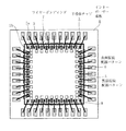
図1に示すように、半導体チップ1は、その回路素子が形成された主面である第1面に複数の端子電極である電極パッド2a、2bを有し、略半数の電極パッド2aが貫通配線部3を介して半導体チップ1の主面の反対側(裏面)の第2面に引き出されて、パッケージ用の配線基板であるインターポーザー基板4の裏面接続配線パターン5と圧接によって接続され、表面に残った電極パッド2bとインターポーザー基板4の表面接続配線パターン6との間はワイヤーボンディング7により接続される。半導体チップ1の全ての電極パッド2a、2bとインターポーザー基板4の配線部である接続配線パターン5、6とが電気的に接続された後、この半導体チップ1をエポキシ樹脂により封止し、例えば、インターポーザー基板4の裏面に設けられたマザーボードとの接続用の電極にはんだボールを接合して半導体パッケージが得られる。
As shown in FIG. 1, the
図2の(a)に示すように、半導体チップ1の裏面側においては、インターポーザー基板4との間に配置した接着剤8を加圧・硬化させ、接着剤8の圧縮応力を用いて、半導体チップ1の裏面に引き出された電極パッド2aを裏面側接続配線パターン5に接続する。フリップチップ接続やC4接続のように、接続後にアンダーフィル材を注入するわけではないので、広い注入用の領域や、半導体チップ1周囲へのアンダーフィルの流れ出し領域を設けなくてもよい。
As shown in FIG. 2A, on the back side of the
半導体チップ1外への接着剤8の流出量は、(半導体チップ面積×押し込み量)であることから、極めて微量であり、また予め供給する接着剤8の量を制御することが可能であることから、安定して流出量をコントロールできる。接着剤8が異方性導電膜やNCP(Non Conductive Past )である場合は、接合時の樹脂の軟化による排出と同時に硬化反応が開始されることから、アンダーフィルのように注入性を向上させるために粘性を下げたことにより流れ出しつづけることがないので、半導体チップ1外への流出量が極めて少ない。
Since the outflow amount of the adhesive 8 to the outside of the
そのため図2の(b)に示すように、半導体チップ1の主面上に残る電極2bと接続されるインターポーザー基板4の表面接続配線パターン6を、半導体チップ1の近傍に設けることが可能となり、ワイヤーボンディング7のワイヤー長を短くしてワイヤーだれやワイヤーショートを防ぐことができる。
Therefore, as shown in FIG. 2B, the surface
このように半導体チップの表裏2面に接続部を振り分けて、一つの面における接続点数を削減し、配線基板側との接続ピッチ差を縮小することで、小型で性能が安定し、しかも低コストな半導体パッケージを実現できる。さらに、半導体チップサイズ下の接続部では樹脂の圧縮応力を用いた異方性導電膜やNCF等を使用することで、半導体チップを配線基板に安定して固着することが可能となる。 In this way, by distributing the connection parts between the front and back surfaces of the semiconductor chip, the number of connection points on one surface is reduced, and the difference in connection pitch with the wiring board is reduced, so that the size is small, the performance is stable, and the cost is low. A simple semiconductor package can be realized. Furthermore, the semiconductor chip can be stably fixed to the wiring substrate by using an anisotropic conductive film, NCF, or the like that uses the compressive stress of the resin at the connection portion below the semiconductor chip size.
その結果、半導体チップの電極パッド数が増大して多ピン化した半導体パッケージやモジュールを低コストで提供することができる。 As a result, the number of electrode pads of the semiconductor chip can be increased to provide a multi-pin semiconductor package or module at low cost.
図1ないし図4は実施例1を示す。半導体チップ1は、図3に示すチップサイズSが6mmであり、主面の電極数すなわち2組の電極パッド2a、2bの総数が600個である。そのため、半導体チップ1の一辺あたりのパッド数は150個(=600/4)、パッドピッチは0.040mm(=6/150)となっている。そこで、電極パッド2a、2bを千鳥配置の2列構成とすることで、1列あたりのパッドピッチを0.08mmにする。本実施例の半導体パッケージは以下の工程で製作される。
1 to 4 show a first embodiment. The
まず、半導体チップ1がウェハー状態の段階で、裏面研削によりウェハー厚みを0.05〜0.25mm程度まで薄くした後、研削された裏面にCVDを用いてSiO2 あるいはSiNを堆積させ厚さ0.5〜2μmの絶縁膜9を裏面全面に設ける。つぎに、エキシマレーザーを用いてウェハーを貫通する貫通配線部3となる穴をφ0.03〜0.1mmで裏面側に引き出す電極パッド2aの数だけ開ける。開ける穴径は、ウェハー厚みと電極パッド数からくるピッチの2つから決められ、ウェハー厚みに対してはアスペクト比(ウェハー厚/穴径)が5以下で、ピッチに対してはピッチ以下となる任意の穴径を選択すればよい。
First, after the
本実施例においては、半数の電極パッド2aを裏面に引き出すこととしたので、1チップあたり300個(=600/2)を穴径0.05mmでウェハー厚0.15mmに開ける。
In this embodiment, since half of the
その後、再びCVDにより穴の側壁にSiO2 あるいはSiNを0.5〜1.0μm堆積させ、穴の側壁にも絶縁膜9を形成する。つぎに電極パッド2a、2bであるAl電極上を含むウェハー全面にPdを下引き層としてNiを数μm無電解メッキにより被覆した後、配線として使用する部分が露出するようにレジストでウェハーの表裏をパターニングした後、Ni層を共通電極としてAuを電解メッキにより0.5〜2μm程度堆積させる。
Thereafter, SiO 2 or SiN is again deposited by 0.5 to 1.0 μm on the side wall of the hole by CVD to form an insulating
レジストを剥離した後、電解メッキにより形成したAuをエッチングレジストとして使用して露出するNiおよびその下のPdを除去することでウェハー表面の電極パッド2aから貫通配線部3を介して裏面にいたる配線10aおよび電極パッド2b上の配線10b(図2および図4参照)が形成される。
Wiring from the
この後ダイシングソーによりウェハーから各半導体チップ1へ分割し、図4の(a)に示す半導体チップ1を形成する。
Thereafter, the wafer is divided into
インターポーザー基板4の表面に形成された裏面接続配線パターン5の半導体チップ1の電極パッド2aと接続する部分には、図4の(b)に示すようにバンプ(突起)11をボールボンディングにより形成し、その表面をスタンピングにより平坦化する。裏面接続配線パターン5は、上記のように一辺あたり半数の電極パッド2aを接続すればよいので、0.08mmピッチであり、配線幅は0.04mm前後となり、十分に配線の平坦性を確保できるので、バンプ高さがばらつき接合時に接合不良を発生させることはない。バンプ高さは、10〜40μmの範囲となる。
Bumps (protrusions) 11 are formed by ball bonding as shown in FIG. 4B on the portion of the back surface
このように形成されたインターポーザー基板4の半導体チップ1を搭載する領域に異方性導電膜からなる接着剤8を配置し、半導体チップ1とインターポーザー基板4とを位置合わせし、その後、半導体チップ1を150℃〜200℃に加熱・加圧することで、異方性導電膜の樹脂を軟化させ、異方性導電膜中に含まれる導電粒子を接合部以外は排出させるとともに、樹脂の熱硬化が開始される。これによって半導体チップ1とインターポーザー基板4とを固着し、その際の圧縮応力を用いた圧接により、裏面側の電極パッド2aの配線10aとバンプ11とを接続する。
An adhesive 8 made of an anisotropic conductive film is disposed in the region of the
接着剤8として配置する異方性導電膜の厚さは、接合後にバンプ11を介してインターポーザー基板4と半導体チップ1との間に形成されるギャップ+10〜20μmのものを使用する。若干厚めにするのは、異方性導電膜に含まれる数μmの導電粒子を樹脂のフローによって押し流すための圧力を発生させるためと、凹凸部を隙間なく埋め込むための樹脂量を確保するためである。本実施例においてはバンプ高さ30μmでギャップが25μmとすることから異方性導電膜の厚みは、40μmのものを使用した。
The thickness of the anisotropic conductive film disposed as the adhesive 8 is a gap of 10 to 20 μm formed between the
そのため、排出される異方性導電膜の量としては、5.0mm×5.0mm×(0.04mm−0.025mm)=0.375mm3 と極めて微量であり、かつ排出と硬化が接合時に同時に開始されることから、流出量は半導体チップ1の周囲0.1〜0.2mm以内に収まってしまう。
Therefore, the amount of the anisotropic conductive film to be discharged is very small as 5.0 mm × 5.0 mm × (0.04 mm−0.025 mm) = 0.375 mm 3 , and discharge and curing are performed at the time of bonding. Since it is started at the same time, the outflow amount falls within 0.1 to 0.2 mm around the
本実施例においては、半導体チップ1の両面に配線10a、10bを有していることから、位置合わせ時においても半導体チップ1のどちらの面も採用できるだけでなく、接合後に半導体チップ1の表面のパターンを確認することで、位置精度が確認できるため、製造時の検査を容易に行うことができる。
In this embodiment, since the
つぎに、インターポーザー基板4に搭載された半導体チップ1の表面に残る半数の電極パッド2bとインターポーザー基板4に設けられた表面接続配線パターン6とをAu線によるワイヤーボンディング7で接続する。
Next, half of the
チップ表面のパッドピッチ0.08mmに対してインターポーザー基板の配線パターンのピッチが同じであれば、接続用の領域としては半導体チップの一辺と同じであるが、配線パターンのピッチが大きい場合は、パッドピッチと配線ピッチの比で広がってしまう。さらに、この広がりは、接続されるパッド数によってより大きくなる。一般にワイヤーボンディングに使用するAu線径が通常20〜25μmであることから接続用配線幅としては、位置ずれを考慮して50μm程度が使用される。そこで配線ピッチとしては0.08〜0.10と若干パッドピッチより大きくなるが、本実施例においては、接続されるパッド数を半分とすることで、広がりを小さくして、Au線の長さを許容範囲である2〜4mm以内に収めることができる。 If the pitch of the wiring pattern of the interposer substrate is the same with respect to the pad pitch of 0.08 mm on the chip surface, the area for connection is the same as one side of the semiconductor chip, but if the pitch of the wiring pattern is large, It spreads with the ratio of pad pitch and wiring pitch. Furthermore, this spread becomes larger with the number of connected pads. In general, since the Au wire diameter used for wire bonding is usually 20 to 25 μm, the connection wiring width is about 50 μm in consideration of positional deviation. Therefore, although the wiring pitch is 0.08 to 0.10, which is slightly larger than the pad pitch, in this embodiment, by reducing the number of connected pads by half, the spread is reduced and the length of the Au wire is reduced. Can be kept within the allowable range of 2 to 4 mm.
この後、エポキシ樹脂にシリカ粒子が含有された封止樹脂を用いてトランスファーモールドにより半導体チップを封止することで、半導体装置である半導体パッケージを得る。 Then, the semiconductor package which is a semiconductor device is obtained by sealing a semiconductor chip by transfer molding using sealing resin in which silica particles are contained in epoxy resin.
本実施例は、半導体チップの両面に電極パッドの接続部を振り分けて、各面から配線基板との接続を行うことで、従来の1面に集中した電極パッドからの接続における課題を解決し、配線基板の配線にかける負担を小さくすることで、低コストで小型の半導体パッケージを実現する。 In this example, electrode pad connection portions are distributed on both sides of the semiconductor chip, and the connection with the wiring substrate is performed from each side, thereby solving the problem in connection from the conventional electrode pad concentrated on one side, By reducing the burden on the wiring of the wiring board, a small semiconductor package can be realized at low cost.
なお、本実施例においては、半導体チップ裏面側の電極接続部とインターポーザー基板との接続に使用するバンプをインターポーザー基板側に設けたが、これは、半導体チップ側に設けてもよい。 In this embodiment, bumps used for connection between the electrode connecting portion on the back side of the semiconductor chip and the interposer substrate are provided on the interposer substrate side. However, this may be provided on the semiconductor chip side.
図5および図6は実施例2を示すもので、本実施例においては、半導体チップ1の信号の高速化に対応するため、信号線の接続を最短化することを目的として、図5の(a)に示すように、半導体チップ1のアクティブ領域の電極パッド2bをフェイスダウンで接続する一方、同図の(b)に示すように、信号の高速化にともないスイッチング電流を供給するために増大の一途をたどっている電源・GND線の電極パッド2aを半導体チップ1の裏面側にまわすことで、半導体チップ1の電極パッド2a、2bを分散させてインターポーザー基板4に接続する。
FIGS. 5 and 6 show the second embodiment. In this embodiment, in order to cope with the increase in the signal speed of the
図6はインターポーザー基板4に半導体チップ1を実装する工程を示すもので、(a)に示すように実施例1と同様に製作された半導体チップ1を上下反転させ、(b)に示すように接着剤8を介してインターポーザー基板4に固定し、その後にワイヤーボンディング7による接続を行う。
FIG. 6 shows a process of mounting the
接着剤8が、異方性導電膜や導電粒子の含まれないNCPである場合の接続抵抗値は、圧接であるため、はんだやワイヤーボンディングのような合金化された接合と比較すれば高いが、デジタル信号においてのインピーダンスとしては抵抗値は問題にならず、それよりも配線長を短くしたことによるL成分削減が効くことになる。また、裏面に回す信号として抵抗成分が問題となるアナログ回路部からの信号をまわすことも可能である。その他の点は実施例1と同様であり、多ピン・高速信号の半導体チップに対応する半導体パッケージを低コストで提供することができる。 When the adhesive 8 is an NCP that does not contain an anisotropic conductive film or conductive particles, the connection resistance value is a pressure contact, so that it is high compared to an alloyed joint such as solder or wire bonding. The resistance value is not a problem as the impedance in the digital signal, and the L component can be reduced by shortening the wiring length. It is also possible to turn a signal from an analog circuit unit whose resistance component is a problem as a signal to be turned to the back surface. The other points are the same as those of the first embodiment, and a semiconductor package corresponding to a semiconductor chip of a multi-pin and high-speed signal can be provided at low cost.
図7および図8は実施例3を示す。本実施例は、図7の(a)、(b)に示すように、実施例1の接着剤8の代わりにNCF(Non Conductive Film )12を用いたものであり、図8の(a)に示すように、半導体チップ1がウェハーの状態でウェハーの裏面に貫通配線部3を介して電極パッド2aを引き出した後に、ウェハー裏面全面にNCF12を貼り合わせる。その後にウェハーをダイシングテープに貼りダイシングソーでウェハーとNCF12を同時に切断する。このように切断されることで、半導体チップ1のチップサイズと同じサイズのNCF12を有する半導体チップ1を製作することができる。
7 and 8 show a third embodiment. In this embodiment, as shown in FIGS. 7A and 7B, an NCF (Non Conductive Film) 12 is used in place of the adhesive 8 of
さらに、通常のフェイスダウン接続では接合される面がNCFにより覆われたことにより接合する面の位置合わせをするターゲットが認識できず接合することができないが、本実施例においては、半導体チップの表面にも電極パッドが存在することから、半導体チップ表面のパターンおよび電極パッドを認識することで、半導体チップ裏面の接合を高精度に行うことができる。 Further, in the normal face-down connection, since the surfaces to be joined are covered with NCF, the target for positioning the surfaces to be joined cannot be recognized and cannot be joined. In addition, since the electrode pad exists, the back surface of the semiconductor chip can be joined with high accuracy by recognizing the pattern and the electrode pad on the surface of the semiconductor chip.
本実施例は、あらかじめ半導体チップに接合材であるNCFを安定して供給できることと、接合工程におけるNCFの貼り合わせ精度が必要でなくなるという利点がある。これによって、さらなるはみ出し量の削減が可能となり、半導体チップ表面側の接続部を半導体チップに近接して配置することができるため、より一層の半導体パッケージの小型化が可能となる。 This embodiment has an advantage that the NCF as a bonding material can be stably supplied to the semiconductor chip in advance, and the NCF bonding accuracy in the bonding process is not necessary. As a result, the amount of protrusion can be further reduced, and the connection part on the semiconductor chip surface side can be arranged close to the semiconductor chip, so that the semiconductor package can be further miniaturized.
1 半導体チップ
2a、2b 電極パッド
3 貫通配線部
4 インターポーザー基板
5 裏面接続配線パターン
6 表面接続配線パターン
7 ワイヤーボンディング
8 接着剤
9 絶縁膜
11 バンプ
12 NCF
DESCRIPTION OF
Claims (3)
Priority Applications (1)
| Application Number | Priority Date | Filing Date | Title |
|---|---|---|---|
| JP2005004706A JP2006196560A (en) | 2005-01-12 | 2005-01-12 | Semiconductor device |
Applications Claiming Priority (1)
| Application Number | Priority Date | Filing Date | Title |
|---|---|---|---|
| JP2005004706A JP2006196560A (en) | 2005-01-12 | 2005-01-12 | Semiconductor device |
Publications (1)
| Publication Number | Publication Date |
|---|---|
| JP2006196560A true JP2006196560A (en) | 2006-07-27 |
Family
ID=36802412
Family Applications (1)
| Application Number | Title | Priority Date | Filing Date |
|---|---|---|---|
| JP2005004706A Pending JP2006196560A (en) | 2005-01-12 | 2005-01-12 | Semiconductor device |
Country Status (1)
| Country | Link |
|---|---|
| JP (1) | JP2006196560A (en) |
Cited By (4)
| Publication number | Priority date | Publication date | Assignee | Title |
|---|---|---|---|---|
| JP2009111307A (en) * | 2007-11-01 | 2009-05-21 | Dainippon Printing Co Ltd | Component built-in wiring board |
| JP2012009717A (en) * | 2010-06-26 | 2012-01-12 | Zycube:Kk | Semiconductor chip and semiconductor module mounting it |
| JP2013085007A (en) * | 2008-09-09 | 2013-05-09 | Lsi Corp | Package supplied power and connected to ground through via |
| US8987901B2 (en) | 2007-11-01 | 2015-03-24 | Dai Nippon Printing Co., Ltd. | Component built-in wiring board and manufacturing method of component built-in wiring board |
-
2005
- 2005-01-12 JP JP2005004706A patent/JP2006196560A/en active Pending
Cited By (4)
| Publication number | Priority date | Publication date | Assignee | Title |
|---|---|---|---|---|
| JP2009111307A (en) * | 2007-11-01 | 2009-05-21 | Dainippon Printing Co Ltd | Component built-in wiring board |
| US8987901B2 (en) | 2007-11-01 | 2015-03-24 | Dai Nippon Printing Co., Ltd. | Component built-in wiring board and manufacturing method of component built-in wiring board |
| JP2013085007A (en) * | 2008-09-09 | 2013-05-09 | Lsi Corp | Package supplied power and connected to ground through via |
| JP2012009717A (en) * | 2010-06-26 | 2012-01-12 | Zycube:Kk | Semiconductor chip and semiconductor module mounting it |
Similar Documents
| Publication | Publication Date | Title |
|---|---|---|
| KR100868419B1 (en) | Semiconductor device and manufacturing method | |
| US8810043B2 (en) | Semiconductor device | |
| KR100856609B1 (en) | A semiconductor device and a method of manufacturing the same | |
| CN102446779B (en) | The manufacture method of semiconductor device | |
| US7728429B2 (en) | Semiconductor device having recessed connector portions | |
| JP4971243B2 (en) | Wiring board | |
| CN101266963B (en) | Wiring board, mounting structure for electronic components, and semiconductor device | |
| JP2002026072A (en) | Method for manufacturing semiconductor device | |
| US6841884B2 (en) | Semiconductor device | |
| JP2011142185A (en) | Semiconductor device | |
| US8889483B2 (en) | Method of manufacturing semiconductor device including filling gap between substrates with mold resin | |
| US7420814B2 (en) | Package stack and manufacturing method thereof | |
| US20090017582A1 (en) | Method for manufacturing semiconductor device | |
| JP2006196560A (en) | Semiconductor device | |
| JP4494249B2 (en) | Semiconductor device | |
| JP2002026073A (en) | Semiconductor device and method of manufacturing the same | |
| JP4708090B2 (en) | Semiconductor device and manufacturing method thereof | |
| JP4910408B2 (en) | Semiconductor device | |
| JP4331179B2 (en) | Semiconductor device | |
| JP2004055660A (en) | Wiring board and semiconductor device | |
| JP5297445B2 (en) | Semiconductor device | |
| JPH10107084A (en) | Semiconductor device and manufacturing method thereof | |
| JP2002217232A (en) | Method for manufacturing semiconductor device | |
| WO2009009566A9 (en) | Method for manufacturing semiconductor device | |
| JP2008021710A (en) | Semiconductor module and manufacturing method thereof |