JP2006003673A - Optical waveguide device, light source device, and optical information processing device - Google Patents
Optical waveguide device, light source device, and optical information processing device Download PDFInfo
- Publication number
- JP2006003673A JP2006003673A JP2004180500A JP2004180500A JP2006003673A JP 2006003673 A JP2006003673 A JP 2006003673A JP 2004180500 A JP2004180500 A JP 2004180500A JP 2004180500 A JP2004180500 A JP 2004180500A JP 2006003673 A JP2006003673 A JP 2006003673A
- Authority
- JP
- Japan
- Prior art keywords
- core
- light
- optical waveguide
- incident
- waveguide device
- Prior art date
- Legal status (The legal status is an assumption and is not a legal conclusion. Google has not performed a legal analysis and makes no representation as to the accuracy of the status listed.)
- Pending
Links
Images


Landscapes
- Optical Integrated Circuits (AREA)
- Led Device Packages (AREA)
Abstract
【課題】 光損失が少なく、小型化や低コスト化が可能で、しかもフィルタによる透過率及び反射率の偏波依存性が小さく、透過させる光の波長と反射させる光の波長をより狭い範囲で切り分けて、波長が異なる複数の光を合波又は分波する光導波路装置、及び、それを用いた、小型ディスプレイ等の点光源装置等として好適な光源装置、並びに光情報処理装置を提供すること。
【解決手段】 辺DEが辺BAと45度の鋭角で交わる五角形ABCDEの形状を有するクラッド3とコア4〜6との接合体からなる光導波路層2を形成する。コア4を辺ABにほぼ垂直に辺ABから辺CDまで直線状に設け、コア5と6を辺DEにほぼ垂直に辺DEからコア4との交差部7又は9まで直線状に設ける。交差部には、コア4を分断して波長選択フィルタ8と10を設ける。合波を行う場合には、光入射又は出射端面11〜13から光を入射し、光出射又は入射端面14から合波光を取り出す。
【選択図】 図1
PROBLEM TO BE SOLVED: To reduce the light loss, reduce the size and cost, and reduce the polarization dependency of the transmittance and reflectance by the filter, so that the wavelength of the transmitted light and the wavelength of the reflected light are narrower. To provide an optical waveguide device that divides and multiplexes or demultiplexes a plurality of lights having different wavelengths, a light source device that is suitable as a point light source device such as a small display using the same, and an optical information processing device .
SOLUTION: An optical waveguide layer 2 comprising a joined body of a clad 3 having a shape of a pentagon ABCDE whose side DE intersects the side BA at an acute angle of 45 degrees and a core 4-6 is formed. The core 4 is provided in a straight line from the side AB to the side CD substantially perpendicular to the side AB, and the cores 5 and 6 are provided in a straight line from the side DE to the intersection 7 or 9 with the core 4 substantially perpendicular to the side DE. At the intersection, the core 4 is divided and wavelength selective filters 8 and 10 are provided. When combining is performed, light is incident from the light incident or exit end faces 11 to 13, and the combined light is extracted from the light exit or incident end face 14.
[Selection] Figure 1
Description
本発明は、波長が異なる複数の光を合波又は分波する光導波路装置、及びそれを用いた、小型ディスプレイ等の点光源装置等として好適な光源装置、並びに光情報処理装置に関するものである。 The present invention relates to an optical waveguide device that multiplexes or demultiplexes a plurality of lights having different wavelengths, a light source device using the same, a light source device suitable as a point light source device such as a small display, and an optical information processing device. .
近年、電子機器、特に携帯用電子機器などは、小型・軽量化と多機能化が求められている。このような傾向の中で、携帯用電子機器においても画像データが扱われるようになっており、精細な画像を見やすく表示する機能をいかにして実現するか、ということが課題となっている。 In recent years, electronic devices, particularly portable electronic devices, have been required to be small and light and have multiple functions. Under such a trend, image data is also handled in portable electronic devices, and how to realize a function of displaying a fine image in an easy-to-view manner has become an issue.
例えば、特表平11−505627号公報などに開示されている網膜ディスプレイは、ユーザーの眼の網膜上に画像を結像させるため、画面表示に占有される面積を少なくすることができ、小型化と高精細度表示とを両立させ得る表示装置として大いに期待されている。この網膜ディスプレイなどの小型ディスプレイでは、光源装置をはじめとしてカラー画像を形成する装置を小型化・軽量化することが今後の課題の1つとなっている。 For example, since the retinal display disclosed in Japanese Patent Publication No. 11-505627 discloses an image formed on the retina of the user's eye, the area occupied by the screen display can be reduced and the size can be reduced. It is highly expected as a display device that can achieve both high-definition display and high-definition display. In a small display such as a retina display, it is one of the future issues to reduce the size and weight of a light source device and other devices that form color images.
従来、フルカラー表示可能なディスプレイ装置の光源として用い得る点光源装置は、例えば特許第3298324号公報に示されているように、発光ダイオード(LED)などの、R(赤)、G(緑)およびB(青)の三原色光を発光する各発光素子からの光を、鏡やレンズを用いて一点に集光し、光源としている。 Conventionally, a point light source device that can be used as a light source of a display device capable of full-color display is, for example, as shown in Japanese Patent No. 3298324, such as a light emitting diode (LED), R (red), G (green), and Light from each light emitting element that emits B (blue) light of the three primary colors is condensed at one point using a mirror or a lens, and used as a light source.
しかし、鏡やレンズを用いる方法は、各発光素子に対して鏡やレンズを精度よく配置して固定する手段が必要になり、実装部品数が多くなるため、光源装置が大きく、重く、コスト高になる問題点がある。また、その製造には、各部品を精度よく実装するために、手間のかかるアライメント工程が必要になり、生産性が低く、大量生産には不向きで、この点からもコスト高になる問題点がある。 However, the method using a mirror and a lens requires a means for accurately arranging and fixing the mirror and the lens with respect to each light emitting element, and the number of mounted parts increases, so the light source device is large, heavy, and expensive. There is a problem that becomes. In addition, the manufacturing requires a time-consuming alignment process to mount each component with high accuracy, which is low in productivity and unsuitable for mass production. is there.
一方、例えば、後述の特許文献1には、光導波路と波長選択フィルタとを用いて波長が異なる複数の光を合波又は分波する光合波分波器が提案されている。
On the other hand, for example,
図12は、特許文献1に従来例として示されている光合波分波器の平面図である。この装置では、シリコン基板100の中央に光導波路層110が設けられ、その両側に外部と光の入出射を行うためのポート101〜103が設けられている。ポート101〜103は光ファイバからなり、シリコン基板100に形成された溝に凹凸嵌合により位置決めされ、接着固定されている。
FIG. 12 is a plan view of an optical multiplexer / demultiplexer disclosed in
光導波路層110には、ポート101〜103のそれぞれに光接続して、導光路であるコア111〜113が設けられている。コア111と113とは、光導波路層110の中心部でほぼ直線状に対向するように配置され、両者を分断するように誘電体多層膜フィルタ114が設けられている。コア112は、コア112から誘電体多層膜フィルタ114に入射して反射された光がコア113に進むように、コア113と交差して設けられている。
The optical waveguide layer 110 is provided with cores 111 to 113 which are light guides, and are optically connected to the
図12に示した装置を光合波器として用いる場合には、合波させようとする入射光121と122とをそれぞれポート101とポート102から入射させ、誘電体多層膜フィルタ114として、入射光121の波長の光は透過させるが、入射光122の波長の光は反射する光学特性をもつものを用いる。このようにすると、ポート101からコア111に入射して伝播してきた入射光121は、誘電体多層膜フィルタ114を透過してコア113に入射する。他方、ポート102からコア112に入射して伝播してきた入射光122は、誘電体多層膜フィルタ114によって反射され、方向変換されてコア113に入射する。この結果、入射光121と122とはいずれもコア113に導かれ、コア113を伝播する中で合波され、ポート103から出射される。
When the apparatus shown in FIG. 12 is used as an optical multiplexer,
図12に示した装置のポート101と102の代わりにLEDなどの光源を設ければ、導波路コアにより簡易に精度良く各光源が出射する光を合波でき、且つ光をコリメートする必要が無いため短い光路で合波でき、低コストで小型集積化した点光源装置を作製することができると期待される。
If light sources such as LEDs are provided instead of the
しかしながら、図12に示した装置では、コア111〜113の光入出射端面を光導波路層110の対向する2辺にのみ設けているので、コア111〜113には必ず曲線部分が含まれる。この場合、コンパクトな光源装置を作製するために光導波路層110を小型化すると、必然的にコア111〜113に曲率の大きい部分が含まれ、漏光による光損失が大きくなり、逆に、光損失を抑えるためにコア111〜113の曲率を小さくすると、光導波路層110が大型化するという二律背反の関係が生じることになる。 However, in the apparatus shown in FIG. 12, the light incident / exit end faces of the cores 111 to 113 are provided only on two opposite sides of the optical waveguide layer 110, so that the cores 111 to 113 always include curved portions. In this case, if the optical waveguide layer 110 is downsized to produce a compact light source device, the cores 111 to 113 inevitably include a portion with a large curvature, resulting in a large light loss due to light leakage. If the curvatures of the cores 111 to 113 are reduced in order to suppress the above, a contradictory relationship occurs in which the optical waveguide layer 110 increases in size.
この対策として、光導波路層の対向する2辺ではなく、互いに直交する2辺に光入射端面を設ければ、コアに曲線部分を設けなくても合波又は分波を行うことのできる構造を形成できると考えられる。 As a countermeasure, if a light incident end face is provided on two sides that are orthogonal to each other instead of two opposite sides of the optical waveguide layer, a structure that can perform multiplexing or demultiplexing without providing a curved portion in the core. It can be formed.
図13は、本発明の比較例である、そのような光導波路装置とそれを用いた光源装置の平面図である。 FIG. 13 is a plan view of such an optical waveguide device and a light source device using the same as a comparative example of the present invention.
この光導波路装置130では、例えばシリコンなどの基板の上にクラッド133とコア134〜136との接合体からなる光導波路層132が形成されている。クラッド133は長方形ABCDの形状を有し、コア134は、辺ABにほぼ垂直に辺ABから辺CDまで直線状に設けられ、コア135および136は、辺DAにほぼ垂直に辺DAからコア134との交差部まで直線状に設けられている。交差部には、コア134を分断してフィルタ137および138が設けられている。フィルタ137および138は、例えば誘電体多層膜からなり、所定の波長範囲の光のみを反射し、他の波長の光を透過させるダイクロイックフィルタである。フィルタ137および138は、それぞれ、コア135および136から入射してフィルタ137および138で反射された光がコア134に進むように、コア134に対する角度が調節されている。
In this optical waveguide device 130, for example, an optical waveguide layer 132 made of a joined body of a clad 133 and
なお、光導波路装置130では、後述する本発明の実施の形態に合わせて、コア134〜136がそれぞれ3本ずつのコア部からなる例を示したが、コア134〜136を構成するコアの数は単一でも複数でもよい。
In the optical waveguide device 130, an example in which the
光源装置140では、光導波路装置130のコア134、135および136の各光入射端面に対向して、それぞれ、赤色光発光素子21、緑色光発光素子22および青色光発光素子23が設けられる。そして、フィルタ137としては赤色光は透過させるが緑色光は反射するものが用いられ、フィルタ138としては赤色光および緑色光は透過させるが青色光は反射するものが用いられる。
In the light source device 140, the red
光源装置140の動作は、次の通りである。赤色光発光素子21、緑色光発光素子22および青色光発光素子23から出射された光は、それぞれ、これらに対向する光入射端面からコア134〜136に取り込まれる。コア134を伝播する赤色光は、フィルタ137を透過し、さらにフィルタ138も透過して、コア134内を光出射端面139へ進む。コア135を伝播する緑色光は、フィルタ137によって反射され、コア135からコア134へ進路を変換されて進み、フィルタ138は透過して、コア134内を光出射端面139へ進む。コア136を伝播してきた青色光は、フィルタ138によって反射され、コア136からコア134へ進路を変換されて、コア134内を光出射端面139へ進む。このようにして、赤色光、緑色光および青色光が、フィルタ138と光出射端面139との間のコア134に導かれるため、この領域を進む中で合波され、合波光が光出射端面139から出射される。
The operation of the light source device 140 is as follows. The lights emitted from the red
このように、光導波路層の互いに直交する2辺に光入射端面を設ければ、コアに曲線部分を設けなくても合波を行うことのできる構造を形成できる。また、図14は光導波路装置130の作製工程の一部を説明する平面図であるが、光導波路装置130は長方形の形状を有するため、図14に示すように、光導波路層が形成されたシリコンウエハ150から一括ダイシングによって無駄なく多数の光導波路装置130を切り出すことができ、この点からも好都合である。 As described above, if the light incident end faces are provided on two mutually orthogonal sides of the optical waveguide layer, a structure capable of multiplexing can be formed without providing a curved portion in the core. FIG. 14 is a plan view for explaining a part of the manufacturing process of the optical waveguide device 130. Since the optical waveguide device 130 has a rectangular shape, an optical waveguide layer is formed as shown in FIG. A large number of optical waveguide devices 130 can be cut out from the silicon wafer 150 without waste by collective dicing, which is also advantageous from this point.
しかしながら、光導波路装置130では、コア135および136からフィルタに入射し反射によって方向変換される際の角度変化が90度であり、フィルタへの入射角は45度になる。LEDのような偏波規定されていない光を、狭い波長範囲で一方の波長の光は透過させ、他方の波長の光は反射させようとする場合、入射光を45度のような大きな角度でフィルタに入射させると、フィルタの反射率及び透過率の偏波依存性が大きくなり、損失が大きくなることが知られている。
However, in the optical waveguide device 130, the angle change when entering the filter from the
本発明は、このような状況に鑑みてなされたものであって、その目的は、光損失が少なく、小型化や低コスト化が可能で、しかもフィルタによる透過率及び反射率の偏波依存性が小さく、透過させる光の波長と反射させる光の波長をより狭い範囲で切り分けて、波長が異なる複数の光を合波又は分波する光導波路装置、及び、それを用いた、小型ディスプレイ等の点光源装置等として好適な光源装置、並びに光情報処理装置を提供することにある。 The present invention has been made in view of such a situation, and the object thereof is to reduce the optical loss, reduce the size and reduce the cost, and further depend on the polarization dependency of the transmittance and the reflectance by the filter. Is divided into a narrower range of the wavelength of light to be transmitted and the wavelength of light to be reflected, and an optical waveguide device that combines or demultiplexes a plurality of lights having different wavelengths, and a small display using the same It is an object to provide a light source device and an optical information processing device suitable as a point light source device or the like.
即ち、本発明は、第1のコアと、この第1のコアに交差する第2のコアとがクラッドに接合されてなり、これらのコアの交差部に前記第1のコアを分断する波長選択フィルタが設けられ、波長が異なる複数の光を合波又は分波する光導波路装置において、
前記第1のコアの光入射又は出射端面を含む前記クラッドの一辺に対し、前記第1の コアがほぼ垂直に延び、前記一辺と対向した前記クラッドの対向辺に前記第1のコアの 光出射又は入射端面を含み、
前記第2のコアの光入射又は出射端面を含む前記クラッドの他の一辺が前記一辺とは 鋭角をなす向きに配置され、前記第2のコアが前記他の一辺にほぼ垂直に前記交差部ま で延びている
ことを特徴とする光導波路装置に係わるものである。
That is, according to the present invention, the first core and the second core intersecting with the first core are joined to the clad, and the wavelength selection for dividing the first core at the intersection of these cores. In an optical waveguide device that is provided with a filter and multiplexes or demultiplexes a plurality of lights having different wavelengths,
The first core extends substantially perpendicular to one side of the clad including the light incident or emission end face of the first core, and the light emission of the first core is on the opposite side of the clad facing the one side. Or including an incident end face,
The other side of the clad including the light incident or exit end face of the second core is disposed in an orientation that forms an acute angle with the one side, and the second core is substantially perpendicular to the other side. The present invention relates to an optical waveguide device characterized in that
また、前記光導波路装置の前記一辺及び前記他の一辺において、少なくとも前記第1のコア及び前記第2のコアの前記光入射端面に対向して光源がそれぞれ配され、前記光源から前記光入射端面に入射した光が合波され、前記対向辺に設けられた前記第1のコアの前記光出射端面から出射される光源装置に係わり、また、前記光導波路装置の前記一辺及び前記他の一辺において、少なくとも前記第1のコア及び前記第2のコアの前記光出射端面に対向して受光素子がそれぞれ配され、前記対向辺に設けられた前記第1のコアの前記光入射端面から入射された光が分波された後、前記受光素子によって受光される第1の光情報処理装置に係わり、更にまた、前記光導波路装置と、この光導波路装置の前記一辺及び前記他の一辺において少なくとも前記第1のコア及び前記第2のコアの前記光入射端面に信号光を入射する光入射手段と、前記対向辺に設けられた前記第1のコアの前記光出射端面から出射される合波光を受ける受光手段とを有する第2の光情報処理装置に係わるものである。 A light source is disposed on each of the one side and the other side of the optical waveguide device so as to face at least the light incident end surfaces of the first core and the second core, and the light incident end surface from the light source. The light incident on the light source device is combined and is emitted from the light emitting end surface of the first core provided on the opposite side, and in the one side and the other side of the optical waveguide device The light receiving elements are arranged to face at least the light emitting end faces of the first core and the second core, respectively, and are incident from the light incident end face of the first core provided on the facing side. After the light is demultiplexed, the first light information processing device is received by the light receiving element, and moreover, the optical waveguide device and at least one side and the other side of the optical waveguide device. Light incident means for inputting signal light to the light incident end faces of the first core and the second core, and multiplexed light emitted from the light emitting end face of the first core provided on the opposite side And a light receiving means for receiving the light.
本発明の光導波路装置によれば、第1のコアと、この第1のコアに交差する第2のコアとがクラッドに接合されてなり、これらのコアの交差部に前記第1のコアを分断する波長選択フィルタが設けられ、前記第1のコアの光入射又は出射端面を含む前記クラッドの一辺に対し、前記第1のコアがほぼ垂直に延び、前記第2のコアの光入射又は出射端面を含む前記クラッドの他の一辺が前記一辺とは鋭角をなす向きに配置され、前記第2のコアが前記他の一辺にほぼ垂直に前記交差部まで延びているので、前記第1のコアと前記第2のコアに曲線部がなければ両者は鈍角で交わることになり、光が前記第1のコアと前記第2のコアとの間で進路を変える際の角度変化は前記鋭角と等しくなり、前記波長選択フィルタで反射される際の入射角は45度未満となる。このため、上述した比較例のように入射角45度でフィルタに入射させる場合に比べ、フィルタの反射率及び透過率の偏波依存性を低減することができ、LEDのような偏波規定されていない光を、狭い波長範囲で一方の波長の光は透過させ、他方の波長の光は反射させようとする場合に起こる光の損失を小さく抑えることができ、透過させる光の波長と反射させる光の波長をより狭い波長範囲で切り分けすることが可能になる。更に、前記光導波路装置では、従来例と異なり、前記第1のコアと前記第2のコアに曲線部を設ける必要がないので、光損失の増加を伴わずに小型化が可能であり、また、鏡やレンズを用いる方法に比べ、生産性が高く、小型軽量化および低コスト化が可能である。 According to the optical waveguide device of the present invention, the first core and the second core intersecting with the first core are joined to the clad, and the first core is connected to the intersection of these cores. A wavelength selection filter is provided to divide, and the first core extends substantially perpendicularly to one side of the clad including the light incidence or emission end face of the first core, and the light incidence or emission of the second core. The other side of the clad including the end face is arranged in an orientation that forms an acute angle with the one side, and the second core extends to the intersecting portion substantially perpendicular to the other side, so that the first core If there is no curved portion in the second core, the two intersect at an obtuse angle, and the angle change when light changes the course between the first core and the second core is equal to the acute angle. The incident angle when reflected by the wavelength selective filter is 4 Less than degrees. For this reason, the polarization dependency of the reflectance and transmittance of the filter can be reduced compared to the case of entering the filter at an incident angle of 45 degrees as in the comparative example described above. The loss of light that occurs when trying to transmit light of one wavelength in a narrow wavelength range and to reflect light of the other wavelength can be suppressed to a small amount, and reflected light with the wavelength of the transmitted light. It becomes possible to isolate | separate the wavelength of light in a narrower wavelength range. Further, unlike the conventional example, the optical waveguide device does not need to be provided with curved portions in the first core and the second core, and thus can be downsized without increasing optical loss. Compared with a method using a mirror or a lens, the productivity is high, and the size and weight can be reduced and the cost can be reduced.
また、本発明の光源装置によれば、前記光導波路装置の前記一辺及び前記他の一辺において、少なくとも前記第1のコア及び前記第2のコアの前記光入射端面に対向して光源がそれぞれ配されており、また、本発明の第1の光情報処理装置によれば、前記光導波路装置の前記一辺及び前記他の一辺において、少なくとも前記第1のコア及び前記第2のコアの前記光出射端面に対向して受光素子がそれぞれ配され、前記対向辺に設けられた前記第1のコアの前記光入射端面から入射された光が分波された後、前記受光素子によって受光され、更にまた、本発明の第2の光情報処理装置によれば、前記光導波路装置と、この光導波路装置の前記一辺及び前記他の一辺において少なくとも前記第1のコア及び前記第2のコアの前記光入射端面に信号光を入射する光入射手段と、前記対向辺に設けられた前記第1のコアの前記光出射端面から出射される合波光を受ける受光手段とを有するので、前記光導波路装置が有する上記の優れた効果を十二分に発揮できる光源装置及び光情報処理装置を提供することができる。 Further, according to the light source device of the present invention, a light source is arranged on each of the one side and the other side of the optical waveguide device so as to face at least the light incident end faces of the first core and the second core. In addition, according to the first optical information processing apparatus of the present invention, the light emission of at least the first core and the second core on the one side and the other side of the optical waveguide device. A light receiving element is arranged opposite to the end face, and light incident from the light incident end face of the first core provided on the opposite side is demultiplexed and then received by the light receiving element. According to the second optical information processing apparatus of the present invention, the light incidence of the optical waveguide device and at least the first core and the second core on the one side and the other side of the optical waveguide device. Signal on end face And the light receiving means for receiving the combined light emitted from the light emitting end face of the first core provided on the opposite side, so that the optical waveguide device has the above excellent It is possible to provide a light source device and an optical information processing device that can fully exhibit the effect.
本発明の光導波路装置において、前記クラッドが少なくとも4辺からなる多角形の形状を有し、前記一辺としての第1辺と前記対向辺としての第3辺とは略平行に配置され、前記第1辺及び前記第3辺とほぼ垂直に第2辺が配置され、前記他の一辺としての第4辺は
前記第1辺と鋭角をなす向きに配置され、前記第1のコアは略直線状に前記第1辺から前記第3辺まで設けられ、前記第2のコアは略直線状に前記第4辺から前記交差部まで設けられているのがよい。
In the optical waveguide device of the present invention, the clad has a polygonal shape including at least four sides, the first side as the one side and the third side as the opposite side are arranged substantially in parallel, The second side is arranged substantially perpendicular to one side and the third side, the fourth side as the other side is arranged in an orientation that forms an acute angle with the first side, and the first core is substantially linear. Preferably, the first side to the third side are provided, and the second core is provided substantially linearly from the fourth side to the intersection.
前記第1辺に設けられた光入射端面から前記第1のコアを伝播してきた第1入射光は、前記波長選択フィルタを透過して先へ進み、他方、前記第4辺に設けられた光入射端面から前記第2のコアを伝播してきた第2入射光は、前記波長選択フィルタによって前記第1のコアへ反射され、前記第1入射光と前記第2入射光とが前記第1のコアで合波され、前記第3辺に設けられた前記第1のコアの光出射端面から出射されるように構成され、又は、前記第3辺に設けられた前記第1のコアの光入射端面から前記第1のコアを伝播してきた入射光が、前記波長選択フィルタを透過して前記第1辺に設けられた前記第1のコアの光出射端面から出射される光と、前記波長選択フィルタによって反射されて前記第4辺に設けられた前記第2のコアの光出射端面から出射される光とに分波されるように構成されているのがよい。 The first incident light that has propagated through the first core from the light incident end face provided on the first side passes through the wavelength selective filter and proceeds forward, while the light provided on the fourth side. The second incident light that has propagated through the second core from the incident end face is reflected to the first core by the wavelength selection filter, and the first incident light and the second incident light are reflected in the first core. And is emitted from the light exit end face of the first core provided on the third side, or the light entrance end face of the first core provided on the third side The incident light that has propagated through the first core from the light passes through the wavelength selective filter and is emitted from the light exit end face of the first core provided on the first side, and the wavelength selective filter The light of the second core that is reflected by the fourth side and provided on the fourth side It is preferable is configured to be light and half wave emitted from the morphism end face.
この際、前記第1のコアが、相前後して配置された複数の前記波長選択フィルタによって複数箇所で分断され、前記第1のコアと交差した少なくとも前記第2のコア及び第3のコアが、前記複数の分断箇所から前記第4辺まで、並行して前記第4辺にほぼ垂直に設けられ、少なくとも前記第3のコアも介して光が合波又は分波されるのがよい。 At this time, the first core is divided at a plurality of locations by a plurality of the wavelength selective filters arranged one after the other, and at least the second core and the third core intersecting the first core In addition, it is preferable that light is multiplexed or demultiplexed through at least the third core from the plurality of division points to the fourth side in parallel and substantially perpendicular to the fourth side.
或いは、前記第1のコアを分断する前記波長選択フィルタの位置から前記第4辺まで前記第2のコアが設けられ、この第2のコアを分断して第2の波長選択フィルタが設けられ、前記第2のコアと交差した第4のコアが、前記第2のコアの分断箇所から前記第1辺まで、前記第1のコアと並行して前記第1辺にほぼ垂直に設けられ、少なくとも前記第4のコアも介して光が合波又は分波されるのがよい。 Alternatively, the second core is provided from the position of the wavelength selection filter that divides the first core to the fourth side, and the second wavelength selection filter is provided by dividing the second core. A fourth core intersecting with the second core is provided substantially perpendicularly to the first side in parallel with the first core from the dividing portion of the second core to the first side; The light may be multiplexed or demultiplexed also through the fourth core.
また、前記第1のコア、前記第2のコア、前記第3のコア及び前記第4のコアが、それぞれ複数のコア部からなるのがよい。複数のコア部を設けると、各コア部を1つのチャンネルに対応させ、多チャンネルの光源装置や情報処理装置を構成できるメリットがある。 The first core, the second core, the third core, and the fourth core may each include a plurality of core portions. Providing a plurality of core parts has an advantage that each core part can correspond to one channel to configure a multi-channel light source device or information processing apparatus.
また、前記多角形が、前記第1辺及び前記第4辺と交わる第5辺を有する五角形であり、前記第2辺の垂直二等分線を対称軸として前記第1辺と前記第3辺、及び前記第4辺と前記第5辺が対称の位置に配置されているのがよい。そして、前記第3辺と前記第4辺とがなす角度が135度であり、前記第4辺と前記第5辺とがなす角度が90度であるのがよい。 The polygon is a pentagon having a fifth side intersecting with the first side and the fourth side, and the first side and the third side with a perpendicular bisector of the second side as an axis of symmetry. And the fourth side and the fifth side are preferably arranged at symmetrical positions. The angle formed by the third side and the fourth side may be 135 degrees, and the angle formed by the fourth side and the fifth side may be 90 degrees.
また、少なくとも前記第1辺と前記第4辺に設けられた各コア端面が傾斜した反射端面に形成され、これらの反射端面を介して、光を各コアの内部又は外部へ導くように構成されているのがよい。 Further, at least the core end surfaces provided on the first side and the fourth side are formed on inclined reflection end surfaces, and the light is guided to the inside or the outside of each core through these reflection end surfaces. It is good to have.
また、前記第1辺、前記第2辺、前記第3辺、前記第4辺及び前記第5辺が、前記各コアと、これらの各コアを設けた共通のクラッド材との切断によって形成されるのがよい。 The first side, the second side, the third side, the fourth side, and the fifth side are formed by cutting the cores and a common clad material provided with the cores. It is better.
本発明の光源装置において、前記光源として発光ダイオード又はレーザーダイオードが用いられるのがよい。 In the light source device of the present invention, a light emitting diode or a laser diode may be used as the light source.
また、前記光源として青色光、緑色光、及び赤色光を発光する光源が用いられるのがよい。これらの発光素子が発する光を合波することで、マルチカラー又はフルカラーの画像を表示することができる。また、それぞれの前記発光素子に駆動電力を供給することによって、搭載された複数の前記発光素子を独立の発光強度で発光させることができる。例えば、赤色光発光素子、緑色光発光素子および青色光発光素子の発光強度を独立に制御することによって、三原色光の混色によるフルカラーの合波光を得ることができる。 In addition, a light source that emits blue light, green light, and red light may be used as the light source. Multi-color or full-color images can be displayed by combining light emitted from these light-emitting elements. Further, by supplying driving power to each of the light emitting elements, the plurality of mounted light emitting elements can emit light with independent light emission intensity. For example, by controlling independently the emission intensities of the red light emitting element, the green light emitting element, and the blue light emitting element, it is possible to obtain full color combined light by mixing three primary color lights.
本発明の第2の光情報処理装置において、前記合波光が走査手段で走査されて投影されるディスプレイとして構成されているのがよい。 The second optical information processing apparatus of the present invention is preferably configured as a display on which the combined light is scanned and projected by scanning means.
以下、本発明の好ましい実施の形態を図面参照下に詳細に説明するが、本発明は下記の例に何ら限定されるものではない。 Hereinafter, preferred embodiments of the present invention will be described in detail with reference to the drawings. However, the present invention is not limited to the following examples.
実施の形態1
実施の形態1は、本発明の光導波路装置の1例である五角形の形状を有する光導波路装置と、この光導波路装置を用いた光源装置とに関するものであり、これらについて図1〜4を用いて説明する。
図1(a)は、実施の形態1に基づく光導波路装置18の平面図である。この光導波路装置18では、例えばシリコンなどの基板1(図示せず)の上にクラッド3とコア4〜6との接合体からなる光導波路層2が形成されており、下部クラッドと上部クラッドとの間に導光路であるコアが埋め込まれている。
FIG. 1A is a plan view of an optical waveguide device 18 based on the first embodiment. In this optical waveguide device 18, for example, an
光導波路層2は、例えば、アクリル系有機溶剤を用いて作製され、クラッド3の屈折率は1.505で、コア4〜6とクラッド3との比屈折率差Δnは0.8%であり、コア4〜6の断面は10μm×10μmの正方形である。光導波路の材料として有機材料系の樹脂を用いることで、光導波路作製プロセスを簡易化できる。例えば、UV(紫外線)硬化型有機材料を用いると、スピンコート等による成膜や、フォトリソグラフィによるコア加工が可能であり、安価な製造設備と低い製造コストでシリコンウエハなどの上に光導波路装置を多数作製することができる。
The
クラッド3は五角形ABCDEの形状を有し、前記第2辺である辺BCの垂直二等分線を対称軸として上下が対称に形成されており、前記一辺又は前記第1辺である辺ABと前記対向辺又は前記第3辺である辺CD、及び前記他の一辺又は前記第4辺である辺DEと前記第5辺である辺EAが、それぞれ等しい長さで対称の位置に配置されている。また、角ABC、角BCDおよび角DEAは90度、角CDEおよび角EABは135度であり、前記他の一辺である辺DEは、延長線上で前記一辺である辺ABと45度の鋭角で交わる。 The clad 3 has a pentagon ABCDE shape, and is vertically symmetric with respect to a perpendicular bisector of the side BC that is the second side, and the side AB that is the one side or the first side. The opposite side or the side CD that is the third side, the other side or the side DE that is the fourth side, and the side EA that is the fifth side are arranged at symmetrical positions with the same length. Yes. Further, the angle ABC, the angle BCD, and the angle DEA are 90 degrees, the angle CDE and the angle EAB are 135 degrees, and the side DE that is the other side is an acute angle of 45 degrees with the side AB that is the one side on the extension line. Intersect.
前記第1のコアであるコア4は、辺ABにほぼ垂直に辺ABから辺CDまで直線状に設けられ、前記第2のコアであるコア5は、辺DEにほぼ垂直に辺DEからコア4との交差部7まで直線状に設けられている。交差部7には、コア4を分断して前記波長選択フィルタであるフィルタ8が設けられている。フィルタ8は、例えば誘電体多層膜からなり、所定の波長範囲の光のみを反射し、他の波長の光を透過させるダイクロイックフィルタである。フィルタ8は、コア5から入射してフィルタ8で反射された光がコア4内に進むように、コア4およびコア5に対する角度が調節されている。
The
さらに、前記第3のコアであるコア6が、辺DEにほぼ垂直に辺DEからコア4との交差部9までコア5に並行して直線状に設けられている。交差部9には、交差部7と同様、コア4を分断して前記波長選択フィルタであるフィルタ10が設けられており、フィルタ10は、例えば誘電体多層膜からなるダイクロイックフィルタである。また、フィルタ10は、コア6から入射してフィルタ10で反射された光がコア4内に進むように、コア4およびコア6に対する角度が調節されている。
Further, the
図1には、コア4〜6がそれぞれ3本ずつのコア部からなる例を示したが、これに限らず、コア4〜6を構成するコアの数は単一でも複数でもよい。複数のコア部を設けると、各コア部を1つのチャンネルに対応させ、多チャンネルの光源装置や情報処理装置を構成できるメリットがある。これは、実施の形態4で後述するヘッドマウントディスプレイなどに応用する際に好都合である。
Although FIG. 1 illustrates an example in which the
辺ABにはコア4の光入射又は出射端面11が設けられ、辺CDにはコア4の光出射又は入射端面14が設けられている。また、辺DEにはコア5の光入射又は出射端面12とコア6の光入射又は出射端面13とが設けられている。これらの光入出射端面は、光導波路装置18が光合波装置として用いられる場合には、光入射又は出射端面11〜13が光入射端面として用いられ、光出射又は入射端面14が光出射端面として用いられる。また、光導波路装置18が光分波装置として用いられる場合には、光出射又は入射端面14が光入射端面として、光入射又は出射端面11〜13が光出射端面として各々用いられる。
The side AB is provided with the light incident or exit end face 11 of the
図1(b)に示した光導波路装置19は、辺GHを光導波路装置18の辺BCに重ねると、この辺に関して光導波路装置18と左右対称の関係にある光導波路装置である。光導波路装置19が光導波路装置18と同等の機能を有することは、明らかである。 The optical waveguide device 19 shown in FIG. 1B is an optical waveguide device that is symmetrical to the optical waveguide device 18 with respect to the side GH when the side GH is overlapped with the side BC of the optical waveguide device 18. It is clear that the optical waveguide device 19 has a function equivalent to that of the optical waveguide device 18.
図2は、光導波路装置18を用いた光源装置20の平面図であり、図3は、図2の2A−2A線の位置における光源装置20の断面図である。
2 is a plan view of the light source device 20 using the optical waveguide device 18, and FIG. 3 is a cross-sectional view of the light source device 20 at the position of
この光源装置20では、コア4の光入射端面11、コア5の光入射端面12およびコア6の光入射端面13に対向して、それぞれ端面発光型のLEDである赤色光発光素子21、緑色光発光素子22および青色光発光素子23が設けられている。そして、フィルタ8として、赤色光は透過させるが緑色光は反射するものが用いられ、フィルタ10として、赤色光および緑色光は透過させるが青色光は反射するものが用いられている。
In this light source device 20, a red
光源装置20の動作は、次の通りである。 The operation of the light source device 20 is as follows.
赤色光発光素子21、緑色光発光素子22および青色光発光素子23は、端子電極25を通じて駆動電力が供給されると、それぞれR(赤)、G(緑)およびB(青)の三原色光を発光する。各発光素子から出射された光は、それぞれ、これらに対向する光入射端面11〜13(図1参照;図2には不図示。)からコア4〜6に取り込まれる。
When the driving power is supplied through the
コア4を伝播する前記第1入射光である赤色光は、フィルタ8を透過し、さらにフィルタ10も透過して、コア4内を光出射端面14へ進む。コア5を伝播する前記第2入射光である緑色光は、フィルタ8によって反射され、コア5からコア4へ進路を変換されて進み、フィルタ10は透過して、コア4内を光出射端面14へ進む。コア6を伝播する前記第3入射光である青色光は、フィルタ10によって反射され、コア6からコア4へ進路を変換されて、コア4内を光出射端面14へ進む。
The red light, which is the first incident light propagating through the
このようにして、赤色光、緑色光および青色光が、フィルタ10と光出射端面14との間のコア4に導かれるため、この領域を進む中で合波され、合波光が光出射端面14から出射される。
Thus, since red light, green light, and blue light are guided to the
本実施の形態では、上記のように、光導波路層の互いに前記鋭角で交わる2辺に光入射端面11〜13を設けるので、コア4〜6に曲線部分を設けなくても入射光を合波できる構造を形成することができる。従来例と異なり、コア4〜6に曲線部を設ける必要がないので、光損失の増加を伴わずに光導波路装置18および光源装置20を小型化できる。
In the present embodiment, as described above, since the light incident end faces 11 to 13 are provided on the two sides of the optical waveguide layer that intersect at the acute angle, incident light is multiplexed without providing curved portions on the
さらに、光がコア5またはコア6からコア4へ進路を変える際の角度変化は前記鋭角、この例では45度と等しくなるので、光がフィルタ8またはフィルタ10で反射される際の入射角は22.5度となる。これは比較例の場合の入射角45度の半分になっているので、比較例に比べフィルタの反射率及び透過率の偏波依存性を低減することができ、LEDのような偏波規定されていない光を、狭い波長範囲で一方の波長の光は透過させ、他方の波長の光は反射させようとする場合に起こる光の損失を小さく抑えることができ、透過させる光の波長と反射させる光の波長をより狭い波長範囲で切り分けすることが可能になる。
Furthermore, since the change in angle when light changes its path from the
本実施の形態の光源装置20は、赤色光発光素子21、緑色光発光素子22および青色光発光素子23から出射されるR(赤)、G(緑)およびB(青)の三原色光を合波してコア端面より出射できる小型点光源装置として機能する。
The light source device 20 of the present embodiment combines the three primary color lights R (red), G (green), and B (blue) emitted from the red
また、光源装置20は、各発光素子に供給する駆動電力を独立に制御することによって、赤色光発光素子21、緑色光発光素子22および青色光発光素子23の発光強度を独立に制御することができ、三原色光の混色によるフルカラーの合波光を得ることができる。この出射ビームは、実施の形態4で後述するフルカラー表示可能な小型ディスプレイ装置の点光源として用いることができる。
Further, the light source device 20 can independently control the emission intensity of the red
図4は光導波路装置18および19の作製工程の一部を説明する平面図である。シリコンウエハ90などの上に光導波路装置18を形成する場合には、一枚のウエハ90からできるだけ多数の光導波路装置を作製できるように、図4(a)に示すように、左右対称の関係にある光導波路装置19と組み合わせ、両者に切り欠き部分である三角形KFAと三角形LDIを加えると、全体として菱形KJLEを形成するようにする。そして図4(b)に示すように、この菱形を面上に隙間なく敷きつめたように光導波路層をパターニングした後、スクライブライン91〜95に沿ってダイシングし、光導波路装置18と光導波路装置19とを個片として切り出すのがよい。
FIG. 4 is a plan view for explaining a part of the manufacturing process of the optical waveguide devices 18 and 19. When the optical waveguide device 18 is formed on a
このように、五角形型の光導波路装置は、無駄になるウエハの領域も少なく、一括ダイシングにより多数の光導波路装置チップ18および19を生産性よく作製することができる。また、ダイシングを行うと、かどの部分に歪みが生じることことがあるが、本実施の形態では歪みの生じにくい辺の部分に光入出射端面を設けているので、ダイシングによる歪みの影響は受けにくい構造になっている。 As described above, the pentagonal optical waveguide device has a small area of a wasted wafer, and a large number of optical waveguide device chips 18 and 19 can be manufactured with high productivity by batch dicing. In addition, when dicing, distortion may occur at the corner, but in this embodiment, the light incident / exit end face is provided at the side where distortion is not likely to occur, so that the influence of distortion due to dicing is affected. It has a difficult structure.
なお、本実施の形態では、辺BAと辺DEが45度の角をなし、角DEAが90度であるので、四辺形KJLEは正方形になるが、一般的な五角形型の光導波路装置を、それと左右対称の関係にある五角形型の光導波路装置とともに一括ダイシングによって切り出すには、四辺形KJLEは菱形でありさえすればよい。ただし、A、F、I、Dは、それぞれ、辺EK、辺KJ、辺JL、辺LEの中点でなければならない。 In this embodiment, the side BA and the side DE form an angle of 45 degrees, and the angle DEA is 90 degrees, so that the quadrangle KJLE is a square, but a general pentagonal optical waveguide device is The quadrilateral KJLE only needs to be a rhombus in order to cut it out by collective dicing together with a pentagonal optical waveguide device having a symmetrical relationship with it. However, A, F, I, and D must be midpoints of the sides EK, KJ, JL, and LE, respectively.
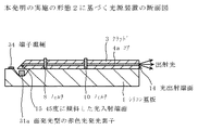
実施の形態2
実施の形態2は、実施の形態1に基づく光導波路装置18の辺ABおよび辺DEの導波路端面に斜め45度加工を施し、コア4〜6の光入射端面を傾斜した反射端面とし、これらの反射端面を介して、光を各コアの内部又は外部へ導くように変更した光導波路装置28とそれを用いた光源装置および光情報処理装置の例である。
In the second embodiment, the waveguide end faces of the side AB and the side DE of the optical waveguide device 18 according to the first embodiment are processed at an angle of 45 degrees so that the light incident end faces of the
このようにすると、面発光型の発光素子や面受光型の受光素子を用いることができる利点がある。例えば、面発光型のLEDは、製造が容易で、安価で、市販されている品種も豊富であり、高周波特性に優れ変調しやすく、実装も容易である。また、フォトトランジスタなどの受光素子も、面受光型の素子が主であり、実装も容易である。 Thus, there is an advantage that a surface light emitting element or a surface light receiving element can be used. For example, surface-emitting LEDs are easy to manufacture, are inexpensive, have a wide variety of commercially available products, have excellent high-frequency characteristics, are easily modulated, and are easy to mount. Also, the light receiving elements such as phototransistors are mainly surface light receiving elements, and are easy to mount.
図5は、実施の形態2に基づく光源装置30の平面図であり、図6は、図5の5A−5A線の位置における光源装置30の断面図である。光源装置30では、45度に傾斜して形成されたコア4の光入射端面15、コア5の光入射端面16およびコア6の光入射端面17に対向して、それぞれ面発光型のLEDである赤色光発光素子31、緑色光発光素子32および青色光発光素子33が設けられている。そして、実施の形態1と同様、フィルタ8として、赤色光は透過させるが緑色光は反射するものが用いられ、フィルタ10として、赤色光および緑色光は透過させるが青色光は反射するものが用いられている。
5 is a plan view of light source device 30 based on the second embodiment, and FIG. 6 is a cross-sectional view of light source device 30 at the position of line 5A-5A in FIG. The light source device 30 is a surface-emitting type LED facing the light
光源装置20の動作は、次の通りである。 The operation of the light source device 20 is as follows.
赤色光発光素子31、緑色光発光素子32および青色光発光素子33は、端子電極34を通じて駆動電力が供給されると、それぞれR(赤)、G(緑)およびB(青)の三原色光を発光する。各発光素子から出射された光は、垂直上方に出射され、それぞれ、これらに対向する45度傾斜光入射端面14〜16により水平方向に光路変換され、コア4〜6内に導かれる。
When the driving power is supplied through the
この後は実施の形態1と同様に、コア4を伝播する赤色光は、フィルタ8を透過し、さらにフィルタ10も透過して、コア4内を光出射端面14へ進む。コア5を伝播する緑色光は、フィルタ8によって反射され、コア5からコア4へ進路を変換されて進み、フィルタ10は透過して、コア4内を光出射端面14へ進む。コア6を伝播する青色光は、フィルタ10によって反射され、コア6からコア4へ進路を変換されて、コア4内を光出射端面14へ進む。
Thereafter, as in the first embodiment, the red light propagating through the
このようにして、赤色光、緑色光および青色光が、フィルタ10と光出射端面14との間のコア4に導かれるため、この領域を進む中で合波され、合波光が光出射端面14から出射される。
Thus, since red light, green light, and blue light are guided to the
本実施の形態の光源装置30では、実施の形態1と同様、光導波路層の互いに前記鋭角で交わる2辺にコア4〜6の光入射端面15〜17を設けるので、コア4〜6に曲線部分を設けなくても入射光を合波できる構造を形成することができ、光損失の増加を伴わずに光導波路装置28および光源装置30の小型化が可能である。さらに、光がフィルタ8またはフィルタ10で反射される際の入射角は22.5度となり、比較例の場合の半分になるため、比較例に比べフィルタの反射率及び透過率の偏波依存性を低減することができ、LEDのような偏波規定されていない光を、狭い波長範囲で一方の波長の光は透過させ、他方の波長の光は反射させようとする場合に起こる光の損失を小さく抑えることができ、透過させる光の波長と反射させる光の波長をより狭い波長範囲で切り分けすることが可能になる。
In the light source device 30 of the present embodiment, as in the first embodiment, the light incident end faces 15 to 17 of the
本実施の形態の光源装置30は、赤色光発光素子31、緑色光発光素子32および青色光発光素子33から出射されるR(赤)、G(緑)およびB(青)の三原色光を合波してコア端面より出射できる小型点光源装置として機能する。また、光源装置30は、各発光素子に供給する駆動電力を独立に制御することによって、赤色光発光素子31、緑色光発光素子32および青色光発光素子33の発光強度を独立に制御することができ、三原色光の混色によるフルカラーの合波光を得ることができる。 The light source device 30 of the present embodiment combines the three primary color lights R (red), G (green), and B (blue) emitted from the red light emitting element 31, the green light emitting element 32, and the blue light emitting element 33. It functions as a small point light source device that can be waved and emitted from the end face of the core. Further, the light source device 30 can independently control the light emission intensities of the red light emitting element 31, the green light emitting element 32, and the blue light emitting element 33 by independently controlling the driving power supplied to each light emitting element. It is possible to obtain a full color combined light by mixing the three primary color lights.
光導波路装置28およびそれと左右対称の光導波路装置29の作製工程は、実施の形態1とほぼ同様であるが、辺ABおよび辺DEの導波路端面に45度傾斜端面を形成するために、ダイシングに関して変更が必要である。すなわち、本実施の形態では、図4において、スクライブライン91と92は、実施の形態1と同様に通常のブレードで切断するが、スクライブライン93、94および95は、V字型ブレードで45度傾斜端面を形成しながら切断する。このようにして、無駄になるウエハの領域も少なく、一括ダイシングにより多数の光導波路装置チップ28および29を生産性よく作製することができる。 The manufacturing process of the optical waveguide device 28 and the optical waveguide device 29 that is symmetrical to the optical waveguide device 28 is substantially the same as in the first embodiment. However, in order to form 45-degree inclined end surfaces on the waveguide end surfaces of the side AB and the side DE, dicing is performed. Needs to be changed. That is, in the present embodiment, in FIG. 4, the scribe lines 91 and 92 are cut with a normal blade as in the first embodiment, but the scribe lines 93, 94 and 95 are 45 degrees with a V-shaped blade. Cutting while forming an inclined end face. In this way, there is little wasted wafer area, and a large number of optical waveguide device chips 28 and 29 can be manufactured with high productivity by batch dicing.
図7は、実施の形態2に基づく情報処理装置40の平面図である。情報処理装置40は、例えば、赤色光、緑色光および青色光からなる入射光を分波して、それぞれの強度を検知する目的などに用いられる。情報処理装置40では、入射光は辺CDに設けられたコア4の光入射端面14から入射され、分波された赤色光、緑色光および青色光は、それぞれ、コア4〜6に設けられた光出射端面15〜17から出射される。
FIG. 7 is a plan view of information processing apparatus 40 based on the second embodiment. The information processing apparatus 40 is used, for example, for the purpose of demultiplexing incident light composed of red light, green light, and blue light and detecting the intensity of each. In the information processing apparatus 40, incident light is incident from the light
光出射端面15〜17は、先述したように、45度に傾斜した反射端面に形成されており、各光出射端面15〜17に対向して、それぞれ、面受光型のフォトトランジスタである赤色光受光素子41、緑色光受光素子42および青色光受光素子43が設けられている。そして、実施の形態1と同様、フィルタ8として、赤色光は透過させるが緑色光は反射するものが用いられ、フィルタ10として、赤色光および緑色光は透過させるが青色光は反射するものが用いられている。
As described above, the light emission end faces 15 to 17 are formed on the reflection end faces inclined by 45 degrees, and face each of the light emission end faces 15 to 17, respectively. A light receiving element 41, a green
情報処理装置40の動作は、次の通りである。 The operation of the information processing apparatus 40 is as follows.
光入射端面14から入射された、赤色光、緑色光および青色光からなる入射光は、コア4を伝播し、フィルタ10に入射する。ここで、入射光に含まれる青色光は、フィルタ10によって反射され、コア4からコア6へ進路を変換されて、コア6内を光出射端面17へ進む。他方、赤色光と緑色光は、フィルタ10を透過して、コア4内を進む。次に、コア4を伝播してきた赤色光と緑色光はフィルタ8に入射し、ここで緑色光はフィルタ8によって反射され、コア4からコア5へ進路を変換されて、コア5内を光出射端面16へ進み、赤色光はフィルタ8を透過して、コア4内を光出射端面15へ進む。そして、各光出射端面15〜17に到達した赤色光、緑色光および青色光は、それぞれ、垂直下方へ反射され、受光素子41〜43によって強度が検知される。
Incident light including red light, green light, and blue light, which is incident from the light
本実施の形態の情報処理装置40では、光導波路層の互いに前記鋭角で交わる2辺にコア4〜6の光出射端面15〜17を設けるので、コア4〜6に曲線部分を設けなくても入射光を分波して出射できる構造を形成することができ、光損失の増加を伴わずに情報処理装置40を小型化することが可能である。さらに、光がフィルタ8またはフィルタ10で反射される際の入射角は22.5度となり、比較例の場合の半分になるため、比較例に比べフィルタの反射率及び透過率の偏波依存性を低減することができ、LEDのような偏波規定されていない光を、狭い波長範囲で一方の波長の光は透過させ、他方の波長の光は反射させようとする場合に起こる光の損失を小さく抑えることができ、透過させる光の波長と反射させる光の波長をより狭い波長範囲で切り分けすることが可能になる。
In the information processing apparatus 40 according to the present embodiment, the light emitting end faces 15 to 17 of the
実施の形態3
実施の形態3は、本発明の光導波路装置の1例である四角形の形状を有する光導波路装置と、この光導波路装置を用いた光源装置とに関するものであり、これらについて図8〜10を用いて説明する。
The third embodiment relates to an optical waveguide device having a rectangular shape, which is an example of the optical waveguide device of the present invention, and a light source device using this optical waveguide device, and FIGS. I will explain.
図8は、実施の形態3に基づく光導波路装置50の平面図である。この光導波路装置50では、例えばシリコンなどの基板1(図示せず)の上にクラッド53とコア54〜56との接合体からなる光導波路層52が形成されており、下部クラッドと上部クラッドとの間に導光路であるコアが埋め込まれている。
FIG. 8 is a plan view of the optical waveguide device 50 based on the third embodiment. In this optical waveguide device 50, for example, an optical waveguide layer 52 made of a joined body of a clad 53 and
光導波路層2は、実施の形態1と同様、例えば、アクリル系有機溶剤を用いて作製され、クラッド53の屈折率は1.505で、コア54〜56とクラッド53との比屈折率差Δnは0.8%であり、コア54〜56の断面は10μm×10μmの正方形である。
As in the first embodiment, the
クラッド53は四角形ABCDの形状を有し、前記一辺又は前記第1辺である辺AB、前記第2辺である辺BC、前記対向辺又は前記第3辺である辺CD、および前記他の一辺又は前記第4辺である辺DAからなる。また、角ABCと角BCDは90度、角CDAは135度であり、前記他の一辺である辺DAは前記一辺である辺BAと45度の鋭角で交わっている。 The clad 53 has a quadrilateral ABCD shape, the side AB being the one side or the first side, the side BC being the second side, the side CD being the opposite side or the third side, and the other side. Or it consists of the side DA which is the fourth side. Further, the angle ABC and the angle BCD are 90 degrees, the angle CDA is 135 degrees, and the side DA that is the other side intersects with the side BA that is the one side at an acute angle of 45 degrees.
前記第1のコアであるコア54は、辺ABにほぼ垂直に辺ABから辺CDまで直線状に設けられ、前記第2のコアであるコア55は、辺DAにほぼ垂直に辺DAからコア54との交差部57まで直線状に設けられている。交差部57には、コア54を分断して前記波長選択フィルタであるフィルタ8が設けられている。フィルタ8は、実施の形態1で既述したように、例えば誘電体多層膜からなり、所定の波長範囲の光のみを反射し、他の波長の光を透過させるダイクロイックフィルタである。フィルタ8は、コア55から入射してフィルタ8で反射された光がコア54内に進むように、コア54およびコア55に対する角度が調節されている。
The
さらに、前記第4のコアであるコア56が、辺ABにほぼ垂直に辺ABからコア55との交差部58までコア54に並行して直線状に設けられている。交差部58には、交差部57と同様、コア55を分断して前記波長選択フィルタであるフィルタ10が設けられており、フィルタ10は、例えば誘電体多層膜からなるダイクロイックフィルタである。また、フィルタ10は、コア56から入射してフィルタ10で反射された光がコア55内に進むように、コア55およびコア56に対する角度が調節されている。
Further, the core 56 as the fourth core is provided in a straight line in parallel with the core 54 from the side AB to the intersection 58 with the core 55 substantially perpendicular to the side AB. Similarly to the crossing portion 57, the crossing portion 58 is provided with a
図8には、コア54〜56がそれぞれ3本ずつのコア部からなる例を示したが、これに限らず、コア54〜56を構成するコアの数は単一でも複数でもよい。複数のコア部を設けると、各コア部を1つのチャンネルに対応させ、多チャンネルの光源装置や情報処理装置を構成できるメリットがある。
FIG. 8 illustrates an example in which the
辺ABには、コア54の光入射又は出射端面61と、コア56の光入射又は出射端面63とが設けられ、辺CDにはコア54の光出射又は入射端面64が設けられている。また、辺DAにはコア55の光入射又は出射端面62が設けられている。これらの光入出射端面は、光導波路装置50が光合波装置として用いられる場合には、光入射又は出射端面61〜63が光入射端面として用いられ、光出射又は入射端面64が光出射端面として用いられる。また、光導波路装置50が光分波装置として用いられる場合には、光出射又は入射端面64が光入射端面として用いられ、光入射又は出射端面61〜63が光出射端面として用いられる。
The side AB is provided with the light incident or exit end face 61 of the
図9は、光導波路装置50を用いた光源装置60の平面図である。この光源装置60では、コア54の光入射端面61、コア55の光入射端面62およびコア56の光入射端面63(61〜63は図8参照;図9には不図示。)に対向して、それぞれ端面発光型のLEDである赤色光発光素子21、緑色光発光素子22および青色光発光素子23が設けられている。そして、フィルタ8としては赤色光は透過させるが緑色光は反射するものが用いられ、フィルタ10としては赤色光および緑色光は透過させるが青色光は反射するものが用いられている。
FIG. 9 is a plan view of a light source device 60 using the optical waveguide device 50. In the light source device 60, the light incident end surface 61 of the core 54, the light
光源装置60の動作は、次の通りである。 The operation of the light source device 60 is as follows.
赤色光発光素子21、緑色光発光素子22および青色光発光素子23は、端子を通じて駆動電力が供給されると、それぞれR(赤)、G(緑)およびB(青)の三原色光を発光する。各発光素子から出射された光は、それぞれ、これらに対向する光入射端面61〜63からコア54〜56に取り込まれる。
The red
コア54を伝播する前記第1入射光である赤色光は、フィルタ8を透過し、さらにフィルタ10も透過して、コア54内を光出射端面64へ進む。コア55を伝播する前記第2入射光である緑色光は、フィルタ10を透過して進み、フィルタ8によって反射されてコア55からコア54へ進路を変換され、コア54内を光出射端面64へ進む。コア56を伝播する前記第3入射光である青色光は、フィルタ10によって反射され、コア56からコア55へ進路を変換されて、フィルタ8によって再び反射され、コア55からコア54へ進路を変換されて、コア54内を光出射端面64へ進む。
The red light that is the first incident light propagating through the core 54 passes through the filter 8 and further passes through the
このようにして、赤色光、緑色光および青色光が、フィルタ8と光出射端面64との間のコア4に導かれるため、この領域を進む中で合波され、合波光が光出射端面64から出射される。
Thus, since red light, green light, and blue light are guided to the
本実施の形態では、上記のように、光導波路層の互いに前記鋭角で交わる2辺に光入射端面を設けるので、コア54〜56に曲線部分を設けなくても入射光を合波できる構造を形成することができる。従来例と異なり、コア54〜56に曲線部を設ける必要がないので、光損失の増加を伴わずに光導波路装置50および光源装置60の小型化が可能である。
In the present embodiment, as described above, since the light incident end faces are provided on the two sides of the optical waveguide layer that intersect at the acute angle, a structure capable of multiplexing incident light without providing curved portions in the
さらに、光がコア55またはコア56からコア54へ進路を変える際の角度変化は前記鋭角、この例では45度と等しくなるので、光がフィルタ8またはフィルタ10で反射される際の入射角は22.5度となる。これは比較例の場合の入射角45度の半分になっているので、比較例に比べフィルタの反射率及び透過率の偏波依存性を低減することができ、LEDのような偏波規定されていない光を、狭い波長範囲で一方の波長の光は透過させ、他方の波長の光は反射させようとする場合に起こる光の損失を小さく抑えることができ、透過させる光の波長と反射させる光の波長をより狭い波長範囲で切り分けすることが可能になる。
Furthermore, since the change in angle when light changes its path from the core 55 or the core 56 to the
本実施の形態の光源装置60は、赤色光発光素子21、緑色光発光素子22および青色光発光素子23から出射されるR(赤)、G(緑)およびB(青)の三原色光を合波してコア端面より出射できる小型点光源装置として機能する。
The light source device 60 of the present embodiment combines the three primary color lights R (red), G (green) and B (blue) emitted from the red
また、光源装置60は、各発光素子に供給する駆動電力を独立に制御することによって、赤色光発光素子21、緑色光発光素子22および青色光発光素子23の発光強度を独立に制御することができ、三原色光の混色によるフルカラーの合波光を得ることができる。この出射ビームは、実施の形態4で後述するフルカラー表示可能な小型ディスプレイ装置の点光源として用いることができる。
Further, the light source device 60 can independently control the light emission intensities of the red
図10は光導波路装置50の作製工程の一部を説明する平面図である。シリコンウエハ90などの上に光導波路装置50を形成する場合には、一枚のウエハ90からできるだけ多数の光導波路装置を作製できるように、図10(a)に示すように、もう1つの光導波路装置50と組み合わせ、両者に切り欠き部分である三角形AD’C’と三角形CA’Dを加えると全体として長方形ABA’B’を形成するように、AB=2CDとする。そしてこの長方形を面上に隙間なく敷きつめたように光導波路層をパターニングして、ダイシングによってスクライブライン96〜99に沿って切断し、個片として光導波路装置50を切り出すのがよい。
FIG. 10 is a plan view for explaining a part of the manufacturing process of the optical waveguide device 50. When the optical waveguide device 50 is formed on the
本実施の形態では角ABCと角BCDとを90度としたので、四辺形ABA’B’は長方形になる。角ABCと角BCDとが直角以外の角であっても、光導波路装置としての機能に変化はないから、一般的には、四辺形ABA’B’は平行四辺形であればよい。この場合にも、一括ダイシングによって切り出すには、AB=2CDであることが必要である。このような四角形型の光導波路装置は、無駄になるウエハの領域も少なく、一括ダイシングにより多数の光導波路装置チップ50を生産性よく作製することができる。 In the present embodiment, since the angle ABC and the angle BCD are 90 degrees, the quadrilateral ABA'B 'is rectangular. Even if the angle ABC and the angle BCD are angles other than a right angle, there is no change in the function as the optical waveguide device. Therefore, in general, the quadrilateral ABA'B 'may be a parallelogram. In this case as well, AB = 2CD is necessary to cut out by batch dicing. Such a rectangular optical waveguide device has a small area of a wasted wafer, and a large number of optical waveguide device chips 50 can be manufactured with high productivity by batch dicing.
なお、実施の形態2と同様に、入射端面61〜63を傾斜端面にしたい場合には、スクライブライン96と97は通常のブレードで切断し、スクライブライン98と99とをV字型ブレードで切断すればよい。 As in the second embodiment, when the incident end surfaces 61 to 63 are to be inclined end surfaces, the scribe lines 96 and 97 are cut with a normal blade, and the scribe lines 98 and 99 are cut with a V-shaped blade. do it.
実施の形態4
上述した実施の形態1〜3の光源装置から出射される合波光は、点光源として利用可能な光である。本実施の形態は、そのような光源装置を網膜ディスプレイなどの小型ディスプレイに適用した例である。
The combined light emitted from the light source devices of
図11は、本発明の実施の形態4に基づくヘッドマウントディスプレイ(HMD)の構成を示す説明図である。このヘッドマウントディスプレイ70では、図5に示した光源装置30から出射される出射光71が、網膜75の上に単位画素を形成する。この際、映像信号に対応して各発光素子に供給する駆動電力を制御することによって、赤色光発光素子21、緑色光発光素子22および青色光発光素子23の発光強度を調節し、三原色光の混色によってフルカラーの表示が可能な単位画素とすることができる。
FIG. 11 is an explanatory diagram showing a configuration of a head mounted display (HMD) based on the fourth embodiment of the present invention. In the head mounted display 70, the emitted light 71 emitted from the light source device 30 shown in FIG. 5 forms unit pixels on the retina 75. At this time, by controlling the driving power supplied to each light emitting element corresponding to the video signal, the emission intensity of the red
そして、光源装置30からの出射光71は、レンズ72等によって走査手段である走査板(scanned image plane)73の上に像を結ばせ、走査板73を通過後、投影光学系のレンズ74等によって、この走査板73と光学的に共役関係にあるユーザーの眼球75の網膜76の上に結像点(スポット)を結ぶように構成されている。この結像点は、映像信号に同期した走査板73の動きによって、網膜76の上で二次元的に走査され、網膜76の上にラスター画像を形成する。ユーザーは、このラスター画像を知覚し、臨場感あふれる映像をパーソナルに体感することができる。 The emitted light 71 from the light source device 30 forms an image on a scanned image plane 73 that is a scanning means by a lens 72 or the like, and after passing through the scanning plate 73, the lens 74 or the like of the projection optical system. Thus, an imaging point (spot) is formed on the retina 76 of the user's eyeball 75 that is optically conjugate with the scanning plate 73. This image formation point is scanned two-dimensionally on the retina 76 by the movement of the scanning plate 73 synchronized with the video signal, and a raster image is formed on the retina 76. The user can perceive the raster image and personally experience a realistic video.
なお、このヘッドマウントディスプレイ70は、サングラスのように装着した状態でプロジェクタやPDA(携帯情報端末)、カメラ、コンピュータ、ゲーム機などに組み込むことにより、コンパクトな映像装置を提供することができる。 The head mounted display 70 can be provided in a compact video device by being incorporated in a projector, a PDA (personal digital assistant), a camera, a computer, a game machine, or the like while wearing like sunglasses.
以上、本発明を実施の形態に基づいて説明したが、本発明はこれらの例に何ら限定されるものではなく、発明の主旨を逸脱しない範囲で適宜変更可能であることは言うまでもない。 As mentioned above, although this invention was demonstrated based on embodiment, it cannot be overemphasized that this invention is not limited to these examples at all, and can be suitably changed in the range which does not deviate from the main point of invention.
例えば、直線上のコアを用いる例のみを示したが、これに限られるものではなく、必要に応じて適宜コアに曲線部を設けてもよい。また、導波路層の形成方法として、一括ダイシングにより個片化する方法を示したが、フォトプロセスでパターニングして個片化したり、スタンピング成型で個片を作製してもよい。 For example, although only an example using a linear core is shown, the present invention is not limited to this, and a curved portion may be appropriately provided in the core as necessary. Further, as a method for forming the waveguide layer, a method of dividing into individual pieces by collective dicing has been shown. However, individual pieces may be formed by patterning by a photo process or by stamping.
本発明の光源装置及び表示装置は、携帯電子機器の表示装置として期待されている網膜ディスプレイ装置などのカラー表示可能な表示装置を、小型、軽量、低コストで提供することに応用することができる。 INDUSTRIAL APPLICABILITY The light source device and the display device of the present invention can be applied to providing a display device capable of color display such as a retinal display device that is expected as a display device of a portable electronic device in a small size, a light weight, and a low cost. .
1…シリコンなどの基板、2…光導波路層、3…クラッド、
4a〜4c、5a〜5c、6a〜6c…コア、7、9…交差部、8、10…フィルタ、
11〜13…光入射又は出射端面、14…光出射又は入射端面、
15〜17…45度に傾斜した光出射又は入射端面、18、19…光導波路装置、
20…光源装置、21a〜21c…端面発光型の赤色光発光素子、
22a〜22c…端面発光型の緑色光発光素子、
23a〜23c…端面発光型の青色光発光素子、24…発光領域、25…端子電極、
28…光導波路装置、30…光源装置、31a〜31c…面発光型の赤色光発光素子、
32a〜32c…面発光型の緑色光発光素子、
33a〜33c…面発光型の青色光発光素子、34…端子電極、40…光情報処理装置、
41a〜41c…赤色光受光素子、42a〜42c…緑色光受光素子、
43a〜43c…青色光受光素子、50…光導波路装置、
54a〜54c、55a〜55c、56a〜56c…コア、57、58…交差部、
61〜63…光入射又は出射端面、70…ヘッドマウントディスプレイ、71…出射光、
73…走査板(scanned image plane)、74…投影光学系のレンズ、
75…ユーザーの眼球、76…網膜、90…シリコンウエハ、
91〜99…スクライブライン、100…シリコン基板、101〜103…ポート、
110…光導波路層、111〜113…コア、114…誘電体多層膜フィルタ、
121、122…入射光、123…出射光、130…光導波路装置、
132…光導波路層、133…クラッド、134〜136…コア、
137、138…フィルタ、139…光出射端面、140…光源装置、
151、152…スクライブライン
DESCRIPTION OF
4a-4c, 5a-5c, 6a-6c ... core, 7, 9 ... intersection, 8,10 ... filter,
11-13 ... Light incident or exit end face, 14 ... Light exit or entrance end face,
15-17: Light emission or incident end face inclined at 45 degrees, 18, 19: Optical waveguide device,
20 ... Light source device, 21a-21c ... End-emitting red light emitting element,
22a to 22c ... green light emitting elements of edge-emitting type,
23a to 23c ... blue light emitting element of edge emitting type, 24 ... light emitting region, 25 ... terminal electrode,
28 ... Optical waveguide device, 30 ... Light source device, 31a to 31c ... Surface emitting red light emitting element,
32a to 32c ... green light emitting element of surface emitting type,
33a to 33c ... surface emitting blue light emitting element, 34 ... terminal electrode, 40 ... optical information processing device,
41a-41c ... red light receiving element, 42a-42c ... green light receiving element,
43a to 43c ... blue light receiving element, 50 ... optical waveguide device,
54a-54c, 55a-55c, 56a-56c ... Core, 57, 58 ... Intersection,
61-63 ... Light incident or exit end face, 70 ... Head mounted display, 71 ... Emitted light,
73: Scanned image plane, 74 ... Lens of projection optical system,
75 ... User's eyeball, 76 ... Retina, 90 ... Silicon wafer,
91-99 ... scribe line, 100 ... silicon substrate, 101-103 ... port,
110 ... Optical waveguide layer, 111-113 ... Core, 114 ... Dielectric multilayer filter,
121, 122 ... incident light, 123 ... outgoing light, 130 ... optical waveguide device,
132: optical waveguide layer, 133: cladding, 134 to 136: core,
137, 138 ... filter, 139 ... light emitting end face, 140 ... light source device,
151, 152 ... scribe line
Claims (16)
前記第1のコアの光入射又は出射端面を含む前記クラッドの一辺に対し、前記第1の コアがほぼ垂直に延び、前記一辺と対向した前記クラッドの対向辺に前記第1のコアの 光出射又は入射端面を含み、
前記第2のコアの光入射又は出射端面を含む前記クラッドの他の一辺が、前記一辺と 鋭角をなす向きに配置され、前記第2のコアが前記他の一辺にほぼ垂直に前記交差部ま で延びている
ことを特徴とする光導波路装置。 A first core and a second core that intersects with the first core are joined to the clad, and a wavelength selective filter that divides the first core is provided at the intersection of these cores, In an optical waveguide device that multiplexes or demultiplexes a plurality of different lights,
The first core extends substantially perpendicular to one side of the clad including the light incident or emission end face of the first core, and the light emission of the first core is on the opposite side of the clad facing the one side. Or including an incident end face,
The other side of the clad including the light incident or emission end face of the second core is arranged in an orientation that forms an acute angle with the one side, and the second core is substantially perpendicular to the other side. An optical waveguide device, characterized in that
前記一辺としての第1辺と前記対向辺としての第3辺とは略平行に配置され、前記第 1辺及び前記第3辺とほぼ垂直に第2辺が配置され、前記他の一辺としての第4辺は前 記第1辺と鋭角をなす向きに配置され、
前記第1のコアは略直線状に前記第1辺から前記第3辺まで設けられ、
前記第2のコアは略直線状に前記第4辺から前記交差部まで設けられている、
請求項1に記載した光導波路装置。 The cladding has a polygonal shape of at least four sides;
The first side as the one side and the third side as the opposite side are arranged substantially in parallel, the second side is arranged substantially perpendicular to the first side and the third side, and the other side as the other side The fourth side is arranged in an orientation that forms an acute angle with the first side,
The first core is provided substantially linearly from the first side to the third side,
The second core is provided substantially linearly from the fourth side to the intersection.
The optical waveguide device according to claim 1.
Priority Applications (3)
| Application Number | Priority Date | Filing Date | Title |
|---|---|---|---|
| JP2004180500A JP2006003673A (en) | 2004-06-18 | 2004-06-18 | Optical waveguide device, light source device, and optical information processing device |
| TW94119084A TWI282451B (en) | 2004-06-18 | 2005-06-09 | Light wave guide device, light source device and light information processor |
| CNB2005100783962A CN1330987C (en) | 2004-06-18 | 2005-06-20 | Light wave guide device,light source device and light information processor |
Applications Claiming Priority (1)
| Application Number | Priority Date | Filing Date | Title |
|---|---|---|---|
| JP2004180500A JP2006003673A (en) | 2004-06-18 | 2004-06-18 | Optical waveguide device, light source device, and optical information processing device |
Publications (1)
| Publication Number | Publication Date |
|---|---|
| JP2006003673A true JP2006003673A (en) | 2006-01-05 |
Family
ID=35772105
Family Applications (1)
| Application Number | Title | Priority Date | Filing Date |
|---|---|---|---|
| JP2004180500A Pending JP2006003673A (en) | 2004-06-18 | 2004-06-18 | Optical waveguide device, light source device, and optical information processing device |
Country Status (3)
| Country | Link |
|---|---|
| JP (1) | JP2006003673A (en) |
| CN (1) | CN1330987C (en) |
| TW (1) | TWI282451B (en) |
Cited By (3)
| Publication number | Priority date | Publication date | Assignee | Title |
|---|---|---|---|---|
| JP2014038174A (en) * | 2012-08-14 | 2014-02-27 | Nippon Telegr & Teleph Corp <Ntt> | Array waveguide diffraction grating type router |
| JP2019035877A (en) * | 2017-08-17 | 2019-03-07 | 日本電信電話株式会社 | Optical integrated circuit |
| WO2021177166A1 (en) * | 2020-03-04 | 2021-09-10 | セーレンKst株式会社 | Optical multiplexing device |
Families Citing this family (6)
| Publication number | Priority date | Publication date | Assignee | Title |
|---|---|---|---|---|
| US9164247B2 (en) * | 2011-07-28 | 2015-10-20 | Source Photonics, Inc. | Apparatuses for reducing the sensitivity of an optical signal to polarization and methods of making and using the same |
| JP2017129744A (en) * | 2016-01-20 | 2017-07-27 | フォトンリサーチ株式会社 | Optical multiplexing device |
| JP7187148B2 (en) * | 2017-12-13 | 2022-12-12 | 日東電工株式会社 | optical waveguide |
| CN109115365A (en) * | 2018-11-14 | 2019-01-01 | 深圳伊讯科技有限公司 | A kind of planar optical waveguide device and temperature measurement system |
| CN115867841A (en) * | 2020-06-26 | 2023-03-28 | 京瓷株式会社 | Optical waveguide package, light emitting device and projection system |
| CN116774508A (en) * | 2022-03-18 | 2023-09-19 | 精工爱普生株式会社 | Projection device |
Family Cites Families (3)
| Publication number | Priority date | Publication date | Assignee | Title |
|---|---|---|---|---|
| JP3298324B2 (en) * | 1994-09-06 | 2002-07-02 | ソニー株式会社 | Image display device |
| CN1150479A (en) * | 1995-02-07 | 1997-05-21 | Ldt激光展示技术公司 | Combination splitting device composed of strip waveguides and uses thereof |
| JPH11295540A (en) * | 1998-04-07 | 1999-10-29 | Japan Aviation Electronics Ind Ltd | 2-wavelength optical multiplexer / demultiplexer |
-
2004
- 2004-06-18 JP JP2004180500A patent/JP2006003673A/en active Pending
-
2005
- 2005-06-09 TW TW94119084A patent/TWI282451B/en not_active IP Right Cessation
- 2005-06-20 CN CNB2005100783962A patent/CN1330987C/en not_active Expired - Fee Related
Cited By (4)
| Publication number | Priority date | Publication date | Assignee | Title |
|---|---|---|---|---|
| JP2014038174A (en) * | 2012-08-14 | 2014-02-27 | Nippon Telegr & Teleph Corp <Ntt> | Array waveguide diffraction grating type router |
| JP2019035877A (en) * | 2017-08-17 | 2019-03-07 | 日本電信電話株式会社 | Optical integrated circuit |
| WO2021177166A1 (en) * | 2020-03-04 | 2021-09-10 | セーレンKst株式会社 | Optical multiplexing device |
| JP2021140005A (en) * | 2020-03-04 | 2021-09-16 | セーレンKst株式会社 | Optical multiplexing device |
Also Published As
| Publication number | Publication date |
|---|---|
| TW200610990A (en) | 2006-04-01 |
| CN1715971A (en) | 2006-01-04 |
| TWI282451B (en) | 2007-06-11 |
| CN1330987C (en) | 2007-08-08 |
Similar Documents
| Publication | Publication Date | Title |
|---|---|---|
| KR102661322B1 (en) | Method and system for textile scanning projector | |
| KR102594052B1 (en) | Method and system for waveguide projector with wide field of view | |
| CN110168419B (en) | Method and system for large field of view display with scanning reflector | |
| JP5693803B1 (en) | Light source device and projection device | |
| KR102549949B1 (en) | Electronic device with multi-element display lighting system | |
| TW201734525A (en) | Optical waveguide element and light source module | |
| KR20170003561A (en) | Multiplexer, image projection device using same, and image projection system | |
| KR20180117181A (en) | A reflective switching device for inputting light of different wavelengths into waveguides | |
| US12443044B2 (en) | Projection substrate and smart glasses | |
| US11555961B1 (en) | Display device with waveguide-based talbot illuminator | |
| US20250035938A1 (en) | Projection substrate and smart glasses | |
| JP2015194549A (en) | Optical device, image projection apparatus, and electronic apparatus | |
| WO2021140752A1 (en) | Video projection device | |
| JP2006003673A (en) | Optical waveguide device, light source device, and optical information processing device | |
| CN111007589A (en) | Waveguide module, display module based on waveguide and near-to-eye display equipment | |
| US12078809B2 (en) | Augmented reality display device | |
| TW202319809A (en) | Display device with waveguide-based talbot illuminator | |
| CN119631006A (en) | Projection optical system and glasses-type terminal | |
| JP2012048071A (en) | Optical multiplexer and image projection device | |
| JP5669210B2 (en) | Display device | |
| KR20180059205A (en) | Directional backlight unit, 3D image display apparatus having the same, and method of manufacturing the same | |
| JP7690723B2 (en) | Method for manufacturing a waveguide and head mounted display having the waveguide | |
| WO2020240798A1 (en) | Optical multiplexing circuit and light source | |
| TWI882296B (en) | Projection substrate and eyeglass type terminal | |
| US20250102806A1 (en) | Virtual image display device and optical unit |
Legal Events
| Date | Code | Title | Description |
|---|---|---|---|
| A977 | Report on retrieval |
Free format text: JAPANESE INTERMEDIATE CODE: A971007 Effective date: 20060907 |
|
| A131 | Notification of reasons for refusal |
Free format text: JAPANESE INTERMEDIATE CODE: A131 Effective date: 20060925 |
|
| A521 | Request for written amendment filed |
Free format text: JAPANESE INTERMEDIATE CODE: A523 Effective date: 20061108 |
|
| A02 | Decision of refusal |
Free format text: JAPANESE INTERMEDIATE CODE: A02 Effective date: 20070118 |
|
| RD13 | Notification of appointment of power of sub attorney |
Free format text: JAPANESE INTERMEDIATE CODE: A7433 Effective date: 20070125 |