JP2005331822A - Image forming apparatus - Google Patents
Image forming apparatus Download PDFInfo
- Publication number
- JP2005331822A JP2005331822A JP2004151685A JP2004151685A JP2005331822A JP 2005331822 A JP2005331822 A JP 2005331822A JP 2004151685 A JP2004151685 A JP 2004151685A JP 2004151685 A JP2004151685 A JP 2004151685A JP 2005331822 A JP2005331822 A JP 2005331822A
- Authority
- JP
- Japan
- Prior art keywords
- charging
- bias
- image
- developer
- forming apparatus
- Prior art date
- Legal status (The legal status is an assumption and is not a legal conclusion. Google has not performed a legal analysis and makes no representation as to the accuracy of the status listed.)
- Withdrawn
Links
Images




Landscapes
- Developing For Electrophotography (AREA)
- Dry Development In Electrophotography (AREA)
- Cleaning In Electrography (AREA)
- Electrostatic Charge, Transfer And Separation In Electrography (AREA)
- Control Or Security For Electrophotography (AREA)
Abstract
【課題】接触帯電を用いたクリーナーレスシステムにおける画像形成装置において、如何なる記録材料を用いた場合でも反転トナーによるカブリが発生せずに、良質な画像を更に長期に亘って維持することができる画像形成装置を提供すること。
【解決手段】バイアス電圧を被帯電体に対向した帯電部材に印加することで被帯電体の帯電を行い、像露光手段によって像露光を行うことにより潜像を形成し、現像剤担持体に担持された現像剤によって該潜像を現像しトナー像を形成する現像手段と、該現像手段が該トナー像を転写材に転写した後に該像担持体に残留した残トナー粒子を回収するクリーニング手段も兼ねる画像形成装置において、正規の極性とは逆の極性の電荷を帯びた現像剤を、前記現像装置で回収する手段を有する。
【選択図】図1In an image forming apparatus in a cleaner-less system using contact charging, an image capable of maintaining a high-quality image for a longer period without fogging due to reversal toner regardless of the recording material used. Providing a forming device.
A charged member is charged by applying a bias voltage to a charging member opposite to the member to be charged, and a latent image is formed by image exposure by an image exposure unit, and is carried on a developer carrier. A developing unit that develops the latent image with the developed developer to form a toner image, and a cleaning unit that collects residual toner particles remaining on the image carrier after the developing unit transfers the toner image to a transfer material. The image forming apparatus also serves as means for collecting the developer having a charge opposite to the normal polarity by the developing device.
[Selection] Figure 1
Description
本発明は、クリーナーレスプロセスの転写式画像形成装置に関する。より詳しくは、電子写真感光体や静電記録誘電体等の像担持体と、該像担持体に対向する帯電部材を有し該帯電部材に帯電バイアスを印加することで像担持体の帯電を行う帯電装置と、該像担持体の帯電処理面に静電潜像を形成する画像情報書き込み装置と、該静電潜像を現像剤により顕像化する現像装置と、該像担持体表面の現像剤を被転写材に移動させる転写装置と、転写装置により被転写材に移動せずに像担持体表面に残留した現像剤は現像装置にて再回収させる方式の複写機・プリンタ等の画像形成装置に関する。 The present invention relates to a transfer-type image forming apparatus using a cleaner-less process. More specifically, an image carrier such as an electrophotographic photosensitive member or an electrostatic recording dielectric, and a charging member facing the image carrier, and a charging bias is applied to the charging member to charge the image carrier. A charging device, an image information writing device that forms an electrostatic latent image on the charging surface of the image carrier, a developing device that visualizes the electrostatic latent image with a developer, and a surface of the image carrier. A transfer device that moves the developer to the transfer material, and an image of a copying machine, a printer, or the like that uses the transfer device to recollect the developer remaining on the surface of the image carrier without being transferred to the transfer material by the transfer device The present invention relates to a forming apparatus.
(a)接触帯電:
電子写真方式や静電記録方式の画像形成装置において、電子写真感光体や静電記録誘電体等の像担持体、その他の被帯電体を所定の極性・電位に帯電処理する帯電手段としては、従来より一般にコロナ帯電器が使用されてきた。これは像担持体(以下、感光体と記す)にコロナ帯電器を非接触に対向配置して、コロナ帯電器から放出されるコロナに感光体面を晒して感光体面を所定の極性・電位に帯電させるものである。近年は、上記の非接触タイプのコロナ帯電器による場合に比べて低オゾン・低電力等の利点を有することから、前記のように、被帯電体としての感光体に電圧(帯電バイアス)を印加した帯電部材(接触帯電部材)を当接させて感光体面を所定の極性・電位に帯電させる接触方式の帯電装置の実用化がなされてきている。特に、帯電部材として導電ローラ(帯電ローラ)を用いたローラ帯電方式の装置が帯電の安定性という点から好ましく用いられている。
(A) Contact charging:
In an electrophotographic or electrostatic recording image forming apparatus, as a charging means for charging an image carrier such as an electrophotographic photosensitive member or an electrostatic recording dielectric, and other charged objects to a predetermined polarity and potential, Conventionally, a corona charger has been generally used. This is done by placing a corona charger in contact with the image carrier (hereinafter referred to as a photoreceptor) in a non-contact manner, exposing the photoreceptor surface to the corona discharged from the corona charger, and charging the photoreceptor surface to a predetermined polarity and potential. It is something to be made. In recent years, since it has advantages such as low ozone and low power compared to the case of the above non-contact type corona charger, as described above, a voltage (charging bias) is applied to the photosensitive member as the member to be charged. A contact-type charging device has been put to practical use in which a charged member (contact charging member) is brought into contact to charge the surface of a photosensitive member to a predetermined polarity and potential. In particular, a roller charging apparatus using a conductive roller (charging roller) as a charging member is preferably used from the viewpoint of charging stability.
又、接触帯電部材として、磁性粒子を担持体に磁気拘束させた磁気ブラシ部を具備させた磁気ブラシ帯電部材(帯電磁気ブラシ、以下、磁気ブラシ帯電器と記す)を用い、該磁気ブラシ帯電器の磁気ブラシ部を感光体に接触させる磁気ブラシ帯電方式の装置も帯電装置の安定性という点から好ましく用いられる。磁気ブラシ帯電器は、導電性の磁性粒子を直接にマグネットに、或はマグネットを内包するスリーブ上に磁気的に拘束させて磁気ブラシ部を形成具備させたものであり、停止或は回転させて磁気ブラシ部を感光体に接触させ、これに電圧を印加することによって感光体の帯電を開始させる。 Further, as the contact charging member, a magnetic brush charging member (charged magnetic brush, hereinafter referred to as a magnetic brush charger) provided with a magnetic brush portion in which magnetic particles are magnetically restrained on a carrier is used. A magnetic brush charging type device in which the magnetic brush portion is brought into contact with the photosensitive member is also preferably used from the viewpoint of the stability of the charging device. The magnetic brush charger has a magnetic brush portion formed by magnetically constraining conductive magnetic particles directly on a magnet or on a sleeve containing the magnet, and is stopped or rotated. The magnetic brush unit is brought into contact with the photoconductor, and a voltage is applied to the photoconductor to start charging the photoconductor.
又、導電性の繊維をブラシ状に形成具備させたもの(ファーブラシ帯電部材、帯電ファーブラシ)、導電性ゴムをブレード状にした導電ゴムブレード(帯電ブレード)等も接触帯電部材として好ましく用いられている。 In addition, a conductive fiber formed in a brush shape (fur brush charging member, charging fur brush), a conductive rubber blade (charging blade) having a conductive rubber blade shape, etc. are preferably used as the contact charging member. ing.
接触帯電の帯電機構(帯電のメカニズム、帯電原理)にはコロナ帯電系と電荷注入(直接帯電)系の2種類の帯電機構が混在しており、どちらが支配的であるかにより各々の特性が現われる。 The contact charging mechanism (charging mechanism, charging principle) has two types of charging mechanisms, a corona charging system and a charge injection (direct charging) system, and each characteristic appears depending on which is dominant. .
コロナ帯電系は接触帯電部材と感光体との微小間隙に生じるコロナ放電現象による放電生成物で感光体表面が帯電する系である。コロナ帯電は、接触帯電部材と感光体に一定の放電しきい値を有するため、帯電電位より大きな電圧を接触帯電部材に印加する必要がある。又、コロナ帯電器に比べれば発生量は格段に少なくないけれども放電生成物を生じる。 The corona charging system is a system in which the surface of the photosensitive member is charged with a discharge product due to a corona discharge phenomenon generated in a minute gap between the contact charging member and the photosensitive member. In corona charging, the contact charging member and the photosensitive member have a certain discharge threshold value, and therefore it is necessary to apply a voltage larger than the charging potential to the contact charging member. In addition, compared with a corona charger, the generated amount is not so small, but a discharge product is generated.
電荷注入帯電系は、接触帯電部材から感光体に直接に電荷が注入されることで感光体表面が帯電する系である。より詳しくは、中抵抗の接触帯電部材が感光体表面に接触して、放電現象を介さずに、つまり放電を基本的に用いないで感光体表面に直接電荷注入を行うものである。よって、接触帯電部材への印加電圧が放電閾値以下の印加電圧であっても、感光体を印加電圧相当の電位に帯電することができる。この電荷注入帯電系はイオンの発生を伴わない。 The charge injection charging system is a system in which the surface of the photoreceptor is charged by directly injecting charges from the contact charging member to the photoreceptor. More specifically, a medium-resistance contact charging member comes into contact with the surface of the photoreceptor, and charge is directly injected into the surface of the photoreceptor without going through a discharge phenomenon, that is, basically without using discharge. Therefore, even when the applied voltage to the contact charging member is an applied voltage that is equal to or lower than the discharge threshold, the photosensitive member can be charged to a potential corresponding to the applied voltage. This charge injection charging system does not involve the generation of ions.
しかし、電荷注入帯電であるため、接触帯電部材の感光体への接触性が帯電性に大きく効いてくる。そこで接触帯電部材はより密に構成し、又、感光体との速度差を多く持ち、より高い頻度で感光体に接触する構成を採る必要があり、この点において接触帯電部材として特に磁気ブラシ帯電器は安定した帯電を行うことができる。 However, because of charge injection charging, the contact property of the contact charging member to the photosensitive member greatly affects the charging property. Therefore, it is necessary to adopt a structure in which the contact charging member is more densely configured and has a large speed difference from the photoconductor, and more frequently contacts the photoconductor. The device can perform stable charging.
磁気ブラシ帯電器による電荷注入帯電は抵抗とコンデンサーの直列回路と等価であると見ることができる、理想的な帯電プロセスでは感光体表面のある点が磁気ブラシと接触している時間(帯電ニップ×感光体の周速)にコンデンサーが充電され、感光体表面電位が印加電圧とほぼ同値になる。 Charge injection charging by a magnetic brush charger can be regarded as equivalent to a series circuit of a resistor and a capacitor. In an ideal charging process, the time during which a point on the surface of the photoreceptor is in contact with the magnetic brush (charging nip × The capacitor is charged to the peripheral speed of the photoconductor, and the surface potential of the photoconductor becomes almost equal to the applied voltage.
導電性の接触部材に電圧を印加し感光体の表面にあるトラップ準位に電荷を注入して感光体の接触帯電を行う方法がある。又、感光体として通常の有機感光体上に導電性微粒子を分散させた表層(電化注入層)を有するものや、アモルファスシリコン感光体等を用いると、接触帯電部材に印加したバイアスのうちの直流成分と略同等の帯電電位を引いた帯電表面に得ることが可能である(特許文献1)。 There is a method in which a voltage is applied to a conductive contact member and a charge is injected into a trap level on the surface of the photoreceptor to charge the photoreceptor. Further, when a photosensitive member having a surface layer (electric injection layer) in which conductive fine particles are dispersed on an ordinary organic photosensitive member or an amorphous silicon photosensitive member is used, a direct current of the bias applied to the contact charging member is used. It is possible to obtain a charged surface with a charging potential substantially equal to that of the component (Patent Document 1).
注入帯電方式は、環境依存性が少ないだけでなく、放電を用いないため、接触帯電部材に対する印加電圧は感光体電位と同程度で十分であり、又、オゾンを発生しない利点があり、完全なオゾンレス且つ低電力消費型帯電が可能となる。
(b)クリーナーレスプロセス(トナーリサイクルプロセス):
又、近年、画像形成装置は小型化が進んできたが、帯電・露光・現像・転写・定着・クリーニング等の作像プロセスの各手段・機器がそれぞれ小型になるだけでは画像形成装置の全体的な小型化には限界があった。又、転写後の感光体上の転写残トナー(残留現像剤)はクリーニング手段(クリーナー)によって回収されて廃トナーとなるが、この廃トナーは環境保護の面からも出ないことが好ましい。
The injection charging method is not only less environmentally dependent, but also uses no discharge, so that the voltage applied to the contact charging member is sufficient to be about the same as the photoreceptor potential, and has the advantage of not generating ozone. Ozone-less and low power consumption type charging becomes possible.
(B) Cleanerless process (toner recycling process):
In recent years, the size of image forming apparatuses has been reduced. However, the overall size of the image forming apparatus can be reduced only by reducing the size of each means and device for the image forming process such as charging, exposure, development, transfer, fixing, and cleaning. There was a limit to the size reduction. Further, the untransferred toner (residual developer) on the photoconductor after the transfer is recovered by a cleaning means (cleaner) and becomes waste toner, but it is preferable that this waste toner does not come out from the viewpoint of environmental protection.
そこで、クリーナーを取り外し、感光体上の転写残トナーは現像手段によって「現像同時クリーニング」で感光体上から除去し現像手段に回収・再用する装置構成にした「クリーナーレスプロセス」の画像形成装置も出現している。現像同時クリーニングとは、転写後に感光体上に若干残留したトナーを次工程以後の現像時にかぶり取りバイアス(現像手段に印加する直流電圧と感光体の表面電位間の電位差であるかぶり取り電位差Vback)によって回収する方法である。この方法によれば、転写残トナーは現像手段に回収されて次工程以後用いられるため、廃トナーを無くし、メンテナンスに手を煩わせることも少なくすることができる。又、クリーナーレスであることでスペース面での利点も大きく、画像形成装置を大幅に小型化できるようになる。更に、感光体の帯電装置が接触帯電性の場合には感光体に接触している帯電部材に転写残トナーを一旦回収させ、それを再び感光体上に吐き出させ現像装置で回収させる。 Therefore, the “cleaner-less process” image forming apparatus is configured such that the cleaner is removed, and the transfer residual toner on the photosensitive member is removed from the photosensitive member by “development simultaneous cleaning” by the developing unit and collected and reused in the developing unit. Has also appeared. Simultaneous development cleaning is a fog removal bias (fogging potential difference Vback which is a potential difference between the DC voltage applied to the developing means and the surface potential of the photosensitive member) during the development after the next process for the toner slightly remaining on the photosensitive member after transfer. It is a method to collect by. According to this method, since the transfer residual toner is collected by the developing means and used after the next step, waste toner can be eliminated and the trouble of maintenance can be reduced. Further, since the cleaner is not required, there is a great advantage in terms of space, and the image forming apparatus can be greatly downsized. Further, when the charging device of the photoconductor is contact charging, the transfer residual toner is once collected by the charging member that is in contact with the photoconductor, and then discharged onto the photoconductor again to be collected by the developing device.
転写残のトナーを被帯電体から除去するためのクリーニング装置を有しない系、所謂クリーナーレスシステムにおいては、接触帯電部材に転写残のトナーが多く混入したり付着したりするため、画像形成耐久において、接触帯電部材の抵抗値が変動が変動する。そこで、耐久枚数や画像比率に応じた帯電部材清掃バイアスを、例えば非作像時に印加して帯電部材の劣化を遅らせるというような方法が知られている。つまり、接触帯電においては、磁気ブラシに混入したりローラーに付着したりしたトナーを感光体上に吐き出し易いバイアス条件やハード構成の条件が存在し、帯電器寿命を延ばすことが可能である。 In a system that does not have a cleaning device for removing the transfer residual toner from the object to be charged, a so-called cleaner-less system, a large amount of transfer residual toner is mixed or adhered to the contact charging member. The resistance value of the contact charging member varies. Therefore, a method is known in which charging member cleaning bias corresponding to the number of durable sheets and the image ratio is applied at the time of non-image formation, for example, to delay the deterioration of the charging member. That is, in the contact charging, there are bias conditions and hardware configuration conditions that make it easy to discharge the toner mixed in the magnetic brush or adhering to the roller onto the photoreceptor, and the life of the charger can be extended.
特に、磁気ブラシ注入帯電装置の場合、正負両極性のトナーが存在すると考えられる転写残トナーを一旦磁気ブラシで回収して前画像の履歴を消すとともに、磁性粒子と回収したトナーの接触摩擦によりトナーを正規の極性に帯電させることにより、再びドラム上にトナーを戻す制御が可能となる。 In particular, in the case of a magnetic brush injection charging device, the transfer residual toner that is considered to have positive and negative polarity toners is once recovered by a magnetic brush to erase the history of the previous image, and the toner by contact friction between the magnetic particles and the recovered toner. Can be controlled to return the toner to the drum again.
又、磁気ブラシ部から感光体ドラムへ吐き出されたトナーは極めて均一な散布状態にあり、又、その量も少量であるため、次の像露光過程に実質的に悪影響を及ぼすことはない。又、転写残トナーパターンに起因するゴースト像の発生もなく、正規極性のトナーは非画像領域においては現像印加バイアスと帯電電位との差により確実に回収することができる。 Further, since the toner discharged from the magnetic brush portion to the photosensitive drum is in a very uniform distribution state, and the amount thereof is small, it does not substantially adversely affect the next image exposure process. Further, there is no ghost image due to the transfer residual toner pattern, and normal polarity toner can be reliably recovered in the non-image area due to the difference between the development bias and the charging potential.
導電性ローラを用いた帯電の場合は、ローラに付着した反対極性トナーを正規極性に戻すために、ローラに摩擦系列が考慮されたシートを当接する等の方法がある。 In the case of charging using a conductive roller, there is a method of bringing a sheet in consideration of a friction series into contact with the roller in order to return the opposite polarity toner attached to the roller to the normal polarity.
しかしながら、このような接触帯電方式を用いたクリーナレス画像形成装置においては、以下のような不具合が生じていた。 However, the following problems have occurred in the cleanerless image forming apparatus using such a contact charging method.
上述のように、転写残トナーは帯電装置において正規の極性、即ち帯電極性と同極性に揃えられて現像で回収されるが、僅かながら、殆ど極性を持たなかったり逆極性のままの状態のトナー(以下、反転トナーと称す)が存在することがある。通常、この逆極性のトナーは極微量であり、仮に現像で回収されずにドラム上を連れ回ることがあっても正規の転写条件においては転写されることなく、又、多くの反転トナーは帯電部材との接触により再び正規の極性を持つことができるため、画像上特に問題にはならない。 As described above, the transfer residual toner is collected by development with a regular polarity, that is, the same polarity as the charging polarity in the charging device, but is slightly but has little or no polarity. (Hereinafter referred to as reversal toner) may exist. Usually, the toner of this reverse polarity is extremely small, and even if it is not recovered by development and is carried around on the drum, it is not transferred under normal transfer conditions, and many reversal toners are charged. Since normal polarity can be obtained again by contact with the member, there is no particular problem on the image.
ところが、使用する記録材料の厚み、表面性によっては画像上の白地部にかぶりとして発生してしまうことがある。この理由については明確ではないが、記録紙の厚みが厚い場合は、転写部における転写ブレード乃至転写ローラの接触圧が強まることにより、逆極性ながらも圧力で転写されてしまうものと考えられる。又、コート紙のように平滑性の高い記録紙においては、記録紙と感光体の密着性が高まるために、同時にトナーが記録紙に押し付けられることを回避する隙間が存在せず、やはり密着度が高まり圧力で転写されるものと考えられる。 However, depending on the thickness and surface properties of the recording material used, it may occur as a fog on a white background on the image. Although the reason for this is not clear, it is considered that when the recording paper is thick, the contact pressure of the transfer blade or the transfer roller in the transfer portion is increased, so that the transfer is performed with the pressure of the opposite polarity. In addition, in recording paper with high smoothness such as coated paper, the adhesion between the recording paper and the photosensitive member is increased, so that there is no gap to avoid the toner being pressed against the recording paper at the same time. Is considered to be transferred by pressure.
反対極性トナーや極性を殆ど持たないトナーは元々或る比率で存在し得るが、特に高湿下でトナーが正規の帯電極性を持ちにくい環境であったり、帯電器内のトナー量が一時的に増加して接触帯電がされにくい状態であったり、又、長期間転写されずにドラム周りを周回しているうちに外添剤が埋め込まれる等、劣化したトナーが増加していった場合に顕著に発生する。それらの反転トナーは、帯電装置内から吐き出されずに蓄積し、或る一定量蓄積すると、それが徐々にドラム上に漏れ出し、現像では回収されないまま圧力転写されてしまうこともある。 The toner of the opposite polarity or the toner having almost no polarity may exist at a certain ratio from the beginning. However, the toner is not likely to have a normal charging polarity under high humidity, or the amount of toner in the charger is temporarily It is noticeable when the amount of deteriorated toner increases, such as when it is in a state where contact charging is difficult to increase, or external additives are embedded while it circulates around the drum without being transferred for a long period of time. Occurs. These reversal toners accumulate without being discharged from the charging device, and when a certain amount is accumulated, they gradually leak onto the drum and may be pressure-transferred without being collected by development.
又、特に厚紙やコート紙を用いる場合において、定着性を維持するためにプロセススピードを遅くするモードを持つ装置の場合、その分転写部において圧力を長時間受けることになるため、現象は更に顕著となる。 In particular, in the case of using thick paper or coated paper, in the case of an apparatus having a mode in which the process speed is slowed down in order to maintain the fixability, the pressure is applied to the transfer portion for a long time. It becomes.
更には、厚紙に限らず長期に亘って使用した場合、現像で回収されず、転写もされない反転トナーは蓄積し、何れは許容量を超え、帯電部材の汚れによる画像不良、飛散や装置の汚れの原因となり、装置そのものの寿命を決定してしまうこともある。 Furthermore, when used over a long period of time, not only for thick paper, the reversal toner that is not collected by development and not transferred is accumulated, and any of these exceeds the allowable amount, and image defects due to charging member contamination, scattering, and device contamination. Cause the life of the device itself to be determined.
そこで、本発明の目的は、接触帯電を用いたクリーナーレスシステムにおける画像形成装置において、如何なる記録材料を用いた場合でも反転トナーによるカブリが発生せずに、良質な画像を更に長期に亘って維持することができる画像形成装置を提供することにある。 SUMMARY OF THE INVENTION Accordingly, an object of the present invention is to maintain a high-quality image for a long period of time in an image forming apparatus in a cleaner-less system using contact charging without causing any fogging due to reversal toner regardless of the recording material used. It is an object of the present invention to provide an image forming apparatus capable of doing so.
以下の構成を採ることにより、上記課題が解決される。 The said subject is solved by taking the following structures.
バイアス電圧を被帯電体に対向した帯電部材に印加することで被帯電体の帯電を行い、像露光手段によって像露光を行うことにより潜像を形成し、現像剤担持体に担持された現像剤によって該潜像を現像しトナー像を形成する現像手段と、該現像手段が該トナー像を転写材に転写した後に該像担持体に残留した残トナー粒子を回収するクリーニング手段も兼ねる画像形成装置において、正規の極性とは逆の極性の電荷を帯びた現像剤を、前記現像装置で回収する手段を有する。 A developer charged on a developer carrying member is formed by applying a bias voltage to a charging member facing the member to be charged to charge the member to be charged, and performing image exposure by an image exposure unit to form a latent image. And developing means for developing the latent image to form a toner image, and an image forming apparatus that also serves as a cleaning means for collecting residual toner particles remaining on the image carrier after the developing means transfers the toner image to a transfer material , The developer having a charge opposite to the normal polarity is collected by the developing device.
前記帯電部材が被帯電体に接触する接触帯電であることが好ましい。 It is preferable that the charging member is contact charging in contact with an object to be charged.
前記帯電部材が磁性粒子と磁性粒子担持体からなることが好ましい。 The charging member is preferably composed of magnetic particles and a magnetic particle carrier.
前記帯電部材が導電性ブラシからなることが好ましい。 The charging member is preferably made of a conductive brush.
前記帯電部材が導電性ゴムローラーからなることが好ましい。 The charging member is preferably made of a conductive rubber roller.
前記帯電方式が、表面に電荷注入層を有する感光体に電圧を印加した導電性部材を当接させて帯電を行う接触帯電方式であることが好ましい。 The charging method is preferably a contact charging method in which charging is performed by bringing a conductive member having a voltage applied into contact with a photoreceptor having a charge injection layer on the surface.
前記正規の極性とは逆の極性の電荷を帯びた現像剤は、接触帯電装置に付着した現像剤であることが好ましい。 The developer having a charge opposite to the normal polarity is preferably a developer attached to the contact charging device.
前記正規の極性とは逆の極性の電荷を帯びた現像剤は、接触帯電装置に回収された乃至混入した現像剤であることが好ましい。 The developer having a charge opposite to the normal polarity is preferably a developer collected or mixed in the contact charging device.
正規の極性とは逆の極性の電荷を帯びた現像剤を、前記現像装置で回収する手段が、帯電電位と現像バイアスの電位差を変化させることが好ましい。 It is preferable that the means for collecting the developer having a charge opposite to the normal polarity by the developing device changes the potential difference between the charging potential and the developing bias.
正規の極性とは逆の極性の電荷を帯びた現像剤を、前記現像装置で回収する手段が、帯電電位と現像バイアスの電位差を小さくすることが好ましい。 Preferably, the means for collecting the developer having a charge opposite to the normal polarity by the developing device reduces the potential difference between the charging potential and the developing bias.
正規の極性とは逆の極性の電荷を帯びた現像剤を、前記現像装置で回収する手段が、現像バイアスの交流成分の波形を変化することが好ましい。 It is preferable that the means for collecting the developer having a charge opposite to the normal polarity by the developing device changes the waveform of the AC component of the developing bias.
正規の極性とは逆の極性の電荷を帯びた現像剤を、前記現像装置で回収する手段が、現像バイアスの交流成分の振幅を変化することが好ましい。 It is preferable that the means for collecting the developer having a charge opposite to the normal polarity by the developing device changes the amplitude of the AC component of the developing bias.
正規の極性とは逆の極性の電荷を帯びた現像剤を、前記現像装置で回収する手段が、現像バイアスの交流成分の振幅を大きくすることが好ましい。 It is preferable that the means for collecting the developer having a charge opposite to the normal polarity by the developing device increases the amplitude of the AC component of the developing bias.
回収した現像剤を帯電部材から被帯電体上に戻すための帯電部材に対して印加する画像形成時とは異なる現像剤戻しバイアスを持つことが好ましい。 It is preferable to have a developer return bias different from that at the time of image formation applied to the charging member for returning the collected developer from the charging member onto the member to be charged.
帯電バイアスが、直流バイアス乃至直流バイアスに交流バイアスを重畳したバイアスであることが好ましい。 The charging bias is preferably a DC bias or a bias in which an AC bias is superimposed on a DC bias.
前記画像形成時とは異なる現像剤戻しバイアスは、交流バイアスの振幅を変化させることが好ましい。 The developer return bias different from that at the time of image formation preferably changes the amplitude of the AC bias.
前記画像形成時とは異なる現像剤戻しバイアスは、交流バイアスの波形を変化させることが好ましい。 It is preferable that the developer return bias different from that at the time of image formation changes the waveform of the AC bias.
選択した被記録材に応じてプロセス速度を変更することが好ましい。 It is preferable to change the process speed in accordance with the selected recording material.
選択した被記録材に応じてプロセス速度を変更することが好ましい。 It is preferable to change the process speed in accordance with the selected recording material.
本発明によれば、クリーナレスの画像形成装置において、帯電バイアスの振幅を大きくし、帯電電位と現像器に印加するDCバイアスの電位差を小さくし、反転トナーを現像器で回収するモードを設定することによって、厚紙、コート紙特有の反転トナーや極性を持たないトナーによるかぶりを防止することができる。 According to the present invention, in the cleanerless image forming apparatus, the charging bias amplitude is increased, the potential difference between the charging potential and the DC bias applied to the developing device is reduced, and the mode for collecting the reversal toner by the developing device is set. As a result, it is possible to prevent fogging due to the reversal toner peculiar to thick paper and coated paper and toner having no polarity.
(1)画像形成装置例(図1):
図1は画像形成装置の概略構成図を示す。本実施の形態に係る画像形成装置は転写式電子写真プロセス利用、電荷注入帯電方式、クリーナーレスプロセスのレーザービームプリンターである。
(1) Example of image forming apparatus (FIG. 1):
FIG. 1 is a schematic configuration diagram of an image forming apparatus. The image forming apparatus according to the present embodiment is a laser beam printer using a transfer type electrophotographic process, a charge injection charging method, and a cleaner-less process.
1は像担持体としての回転ドラム型の電子写真感光体(以下、感光ドラムと記す)である。本実施の形態の感光ドラム1は負帯電性・電荷注入帯電性のOPC感光体(有機光導電性感光体)であり、矢示の時計方向aに150mm/secのプロセススピード(周速度)で回転駆動される。
2は感光ドラム1の面を所定の極性・電位に一様に帯電処理する接触帯電装置である。本実施の形態では、磁気ブラシ帯電装置であり、回転する感光ドラム1の面はこの磁気ブラシ帯電装置2によりほぼ−700Vに電荷注入帯電方式で一様に帯電処理される。
A
3は画像情報露光手段(露光装置)であり、本実施の形態ではレーザービームスキャナーである。このレーザービームスキャナー3は、半導体レーザー、ポリゴンミラー、F−θレンズ等を有して成り、CCD等の光電変換素子を有する原稿読み取り装置、電気計算機、ワードプロセッサー等の不図示のホスト装置から入力する目的の画像情報の時系列電気デジタル画像信号に対応して変調されたレーザー光Lを射出して、回転感光体ドラム1の一様帯電処理面をレーザー光走査露光する。このレーザー光走査露光により回転感光ドラム1の周面に目的の画像情報に対応した静電潜像が形成される。
Reference numeral 3 denotes an image information exposure means (exposure device), which is a laser beam scanner in the present embodiment. The laser beam scanner 3 includes a semiconductor laser, a polygon mirror, an F-θ lens, and the like, and inputs from an unillustrated host device such as a document reading device, an electric computer, or a word processor having a photoelectric conversion element such as a CCD. The laser beam L modulated in accordance with the time-series electric digital image signal of the target image information is emitted, and the uniformly charged surface of the rotating
4は現像装置である。本実施の形態では、重合法で作製した転写残トナーの少ない高離型性球形トナーと、磁性キャリアを混合した現像剤による2成分接触現像方式の現像装置を用いている。そして、回転感光体ドラム1面の静電潜像をトナー像として反転現像させている。
5は感光ドラム1の下側に配置した転写装置であり、本実施の形態の該転写装置は転写ベルトタイプである。5aは無端状のの転写ベルト(例えば、膜厚75μmのポリイミドのベルト)であり、駆動ローラ5bと従動ローラ5c間に懸回張設されていて、感光体ドラム1の回転方向に順方向に感光ドラム1の回転速度とほぼ同じ周速度で回動される。5dは転写ベルト5aの内側に配設した導電性ブレードであり、転写ベルト5aの上行側ベルト部分を感光ドラム1の下面部分に加圧して転写部位としての転写ニップ部Tを形成させている。
Reference numeral 5 denotes a transfer device disposed below the
6は給紙カセットであり、紙等の被転写材Pを積載収納させてある。給紙ローラ7の駆動により給紙カセット6内に積載収納の被転写材Pが1枚分離給しされ、搬送ローラ8等を含むシートパス9を通って所定の制御タイミングにて回転感光ドラム1と転写装置5の転写ベルト5aとの間の転写ニップ部Tに給送される。
Reference numeral 6 denotes a paper feed cassette in which a transfer material P such as paper is stacked and stored. One sheet of transfer material P loaded and stored in the sheet cassette 6 is separated and fed by the drive of the sheet feed roller 7, passes through the sheet path 9 including the
転写ニップ部Tに給送された被転写材Pは、回転感光体ドラム1と転写ベルト5aの間を挟持搬送され、その間、導電性ブレード5dに転写バイアス印加電源E5から所定の転写バイアスが印加されて、被転写材Pの裏面からトナーと逆極性の帯電がなされる。これにより、転写ニップ部Tを通る被転写材Pの表面側に回転感光ドラム1面側のトナー像が順次に静電転写されていく。
The material P to be transferred fed to the transfer nip T is nipped and conveyed between the rotating
転写ニップ部Tを通ってトナー像の転写を受けた被転写材Pは、回転感光ドラム1面から順次に分離されてシートパス10を通って定着装置(例えば熱ローラ定着装置)11に導入されてトナー像の定着処理を受けてプリントアウトされる。
The transfer material P that has received the transfer of the toner image through the transfer nip T is sequentially separated from the surface of the rotary
本実施の形態のプリンターはクリーナーレスプロセスであり、転写ニップ部Tで被転写材Pに転写されずに回転感光体ドラム1の表面に残ったトナーを除去する専用のクリーナーは配置していないが、転写残トナーは、後述するように、引き続く感光ドラム1の回転で磁気ブラシ帯電装置2の位置に至り、感光ドラム1に接触している接触帯電部材としての磁気ブラシ帯電器2Aの磁気ブラシ部に一時的に回収され、その回収トナーが再び感光ドラム1面に吐き出されて最終的に現像装置4に回収され感光ドラム1は繰り返して作像に供される。
The printer according to the present embodiment is a cleaner-less process, and a dedicated cleaner for removing toner remaining on the surface of the rotating
12は転写装置5と磁気ブラシ帯電装置2との間において感光ドラムに当接させ、ACバイアス、帯電と逆極性のDCバイアス、又はACバイアスを重畳した帯電と逆極性のDCバイアスを印加した導電性ブラシであり、磁気ブラシ帯電装置2による帯電直前の感光体ドラム表面電位をならすと同時に、転写残トナーを除電、若しくは感光体ドラムの帯電と逆極性に帯電して、磁気ブラシ帯電器2Aの磁気ブラシ部での回収を容易にする。
(2)クリーナーレスプロセス:
本実施の形態のプリンタは、クリーナーレスプロセスであるから、被転写材Pに対するトナー像転写後の感光体ドラム1に残留したトナー(転写残トナー)は感光体ドラム1の帯電ニップ部Nに持ち運ばれて磁気ブラシ接触帯電装置2の磁気ブラシ帯電器2Aの磁気ブラシ部2cに混入して一時的に回収される。感光ドラム1上の転写残トナーは、転写時の剥離放電等により、極性が正のものと負のものが混在していることが多い。この極性が混在した転写残トナーが磁気ブラシ帯電器2Aに至って磁気ブラシ部2c内に混入して一時的に回収される。この転写残トナーの磁気ブラシ帯電器2Aの磁気ブラシ部2cへの取り込みは、磁気ブラシ帯電器2AにAC成分を印加することで、磁気ブラシ帯電器2Aと感光体ドラム1間の振動電界効果によってより効果的に行わせることができる。
(2) Cleanerless process:
Since the printer of this embodiment is a cleaner-less process, the toner (transfer residual toner) remaining on the
そして、磁気ブラシ部14内に取り込まれた転写残トナーは、極性が全て負に帯電されて感光体ドラム1上に吐き出される。極性が揃えられて感光体ドラム1上に吐き出された転写残トナーは、現像部mに至って現像装置4の現像4bにより現像時のかぶり取り電界によって現像同時クリーニングで回収される。この転写残トナーの現像同時回収は、回転方向の画像領域が感光体ドラム1の周長よりも長い場合には、その他の帯電、露光、現像、転写といった画像形成工程と同時進行で行われる。これにより転写残トナーは現像装置4内に回収されて次工程以後も用いられるため、廃トナーを無くすことができる。又、スペースの面での利点も大きく、画像形成装置の大幅な小型化が可能となる。
Then, the transfer residual toner taken into the magnetic brush unit 14 is charged negatively in all polarities and discharged onto the
現像剤のトナーtとして重合法で作製した高離型性球形トナーを用いることで、転写残トナーの発生量を少なくすることができるし、又、磁気ブラシ帯電器2Aから吐き出されたトナーの現像装置4への回収性を向上させることができる。2成分接触現像方式の現像装置4を用いることでも磁気ブラシ帯電器2Aから吐き出されたトナーの現像装置4への回収性を向上させている。ここで、通常、トナーは電気抵抗が比較的高いから、磁気ブラシ帯電器2Aの磁気ブラシ部14にそのようなトナー粒子が混入することは磁気ブラシ部2cの電気抵抗を上昇させて帯電能を低下させる因子であり、混入トナー量が比較的多い場合は、非作像時に大量のトナーを吐き出すことで、良好な帯電を維持することができる。
By using a highly releasable spherical toner prepared by a polymerization method as the toner t of the developer, the amount of transfer residual toner can be reduced, and the development of the toner discharged from the
ここでトナー吐き出しについて簡単に説明する。 Here, the toner discharge will be briefly described.
磁気ブラシ部にトナーが混入した場合、それの電気抵抗は次第に大きくなっていくため、帯電ニップ通過中に充分な電荷の移動が行われず、帯電ニップ通過後の感光体表面電位は印加電圧より小さくなってしまう。以下、感光体表面電位と印加電圧との電位差をΔVとする。磁気ブラシ帯電器に取り込まれたトナーが磁気ブラシキャリアとの接触により感光体電位と同極の電荷を付与されている場合、電位差ΔVによって発生する電界により混入トナーは磁気ブラシ中から感光体表面に吐き出される。特開平9−0096949号公報等に開示されるように、この現象を利用した、非作像時(非画像形成時)に帯電バイアスのAC成分(交流成分)の振幅Vppを減少させたり、AC成分の印加を停止させることで電位差ΔVを大きくし、積極的にトナーを吐き出させて磁気ブラシの電気抵抗上昇を抑えている。 When toner is mixed into the magnetic brush part, its electric resistance gradually increases, so that sufficient charge movement is not performed while passing through the charging nip, and the photoreceptor surface potential after passing through the charging nip is smaller than the applied voltage. turn into. Hereinafter, the potential difference between the photoreceptor surface potential and the applied voltage is represented by ΔV. When the toner taken in the magnetic brush charger is charged with the same polarity as the photosensitive member potential by contact with the magnetic brush carrier, the mixed toner is transferred from the magnetic brush to the photosensitive member surface by the electric field generated by the potential difference ΔV. Exhaled. As disclosed in Japanese Patent Laid-Open No. 9-0096949 and the like, this phenomenon is used to reduce the amplitude Vpp of the AC component (AC component) of the charging bias during non-image formation (non-image formation) or AC By stopping the application of the component, the potential difference ΔV is increased, and the toner is actively discharged to suppress an increase in the electric resistance of the magnetic brush.
上述の非作像時の吐き出しとしては、紙間や作像動作終了後の後回転等で行うことで、長期の使用において磁気ブラシ中の混入トナー量を一定以下に保つことが可能となる。 The discharge at the time of non-image formation is performed by inter-paper or post-rotation after completion of the image formation operation, so that the amount of toner mixed in the magnetic brush can be kept below a certain level for long-term use.
又、磁気ブラシ部14から感光体ドラム1へ吐き出されたトナーは極めて均一な散布状態にあり、又、その量も少量であるため、次の像露光過程に実質的に悪影響を及ぼすことはない。又、転写残トナーパターンに起因するゴースト像の発生もない。
(3)動作シーケンス(図2):
次に、動作シーケンスを説明する。
Further, since the toner discharged from the magnetic brush portion 14 to the
(3) Operation sequence (FIG. 2):
Next, an operation sequence will be described.
a.前多回転工程:
プリンタの始動動作期間(起動動作期間、ウォーミング期間)である。メイン電源スイッチ−オンにより、装置のメインモーターを駆動させて感光体ドラムを回転駆動させ、所定のプロセス機器の準備動作を実行させる。
a. Pre-multi-rotation process:
This is a printer start-up operation period (start-up operation period, warming period). When the main power switch is turned on, the main motor of the apparatus is driven to rotate the photosensitive drum, and a predetermined operation of the process equipment is executed.
b.前回転工程:
プリント前動作を実行させる期間である。個の前回転工程は前多回転工程中にプリント信号が入力したときには前多回転工程に引き続いて実行される。プリント信号の入力がないときには前多回転工程の終了後にメインモーターの駆動が一旦停止されて感光体ドラムの回転駆動が停止され、プリンタはプリント信号が入力されるまでスタンバイ(待機)状態に保たれる。プリント信号が入力すると、前回転工程が実行される。
b. Pre-rotation process:
This is the period during which the pre-print operation is executed. The individual pre-rotation steps are executed subsequent to the pre-multi-rotation step when a print signal is input during the pre-multi-rotation step. When the print signal is not input, the drive of the main motor is temporarily stopped after the completion of the previous multi-rotation process, the rotation of the photosensitive drum is stopped, and the printer is kept in a standby (standby) state until the print signal is input. It is. When the print signal is input, the pre-rotation process is executed.
c.印字工程(画像形成工程、作像工程):
所定の前回転工程が終了すると、引き続いて回転感光ドラムに対する作像プロセスが実行され、回転感光ドラム面に形成されたトナー像の被転写材への転写、定着手段によるトナー像の定着処理がなされて画像形成物がプリントアウトされる。連続印字(連続プリント)モードの場合は上記の印字工程が所定の設定プリント枚数分繰り返して実行される。
c. Printing process (image forming process, image forming process):
When the predetermined pre-rotation process is completed, an image forming process for the rotating photosensitive drum is subsequently performed, and the toner image formed on the surface of the rotating photosensitive drum is transferred to the transfer material, and the toner image is fixed by the fixing unit. The image formation is printed out. In the case of the continuous printing (continuous printing) mode, the above printing process is repeated for a predetermined set number of prints.
d.紙間工程:
連続印字モードにおいて一の被転写材の後端部が転写ニップ部を通過した後、次の被転写材の先端部が転写ニップ部に到達するまでの間の、転写ニップ部における被転写材の非通紙状態期間である。この期間に転写ニップを通過する回転感光体の領域がその前に帯電ニップ部を通過する間は、帯電バイアスのAC成分の振幅を変更し、磁気ブラシ帯電部材で一時的に回収した転写残トナーを回転感光体ドラム面に吐き出すし、現像器で回収する。
d. Inter-sheet process:
In the continuous printing mode, after the trailing edge of one transfer material passes through the transfer nip, the transfer material in the transfer nip until the leading edge of the next transfer material reaches the transfer nip. This is a non-paper passing period. During this period, while the area of the rotating photoconductor passing through the transfer nip passes through the charging nip portion, the AC component amplitude of the charging bias is changed, and the transfer residual toner temporarily collected by the magnetic brush charging member Is discharged to the surface of the rotating photosensitive drum and collected by a developing device.
e.後回転工程:
最後の被転写材の印字工程が終了した後もしばらくの間メインモータの駆動を継続させて感光体ドラムを回転駆動させ、所定の後動作を実行させる期間である。この期間においても紙間工程と同様に帯電バイアスのAC成分の振幅を変更することで、磁気ブラシ帯電部材で一時的に回収した転写残トナーを回転感光体ドラム面に吐き出し、現像器で回収する。
e. Post-rotation process:
This is a period during which a predetermined post-operation is executed by continuing to drive the main motor for a while after the printing process of the last transfer material is completed and rotating the photosensitive drum. Also during this period, by changing the amplitude of the AC component of the charging bias in the same manner as the inter-sheet process, the transfer residual toner temporarily collected by the magnetic brush charging member is discharged to the surface of the rotating photosensitive drum and collected by the developing device. .
f.スタンバイ:
所定の後回転工程が終了すると、メインモータの駆動が停止され感光体ドラムの回転駆動が停止され、プリンタは次のプリントスタート信号が入力するまでスタンバイ状態に保たれる。
f. stand-by:
When the predetermined post-rotation process is completed, the driving of the main motor is stopped, the rotation of the photosensitive drum is stopped, and the printer is kept in a standby state until the next print start signal is input.
1枚だけのプリントの場合は、そのプリント終了後、プリンタは後回転工程を経てスタンバイ状態になる。スタンバイ状態においてプリントスタート信号が入力すると、プリンターは前回転工程に移行する。 In the case of printing only one sheet, after the printing is finished, the printer goes into a standby state through a post-rotation process. When a print start signal is input in the standby state, the printer shifts to a pre-rotation process.
cの印字工程時が画像形成時であり、aの前多回転工程、bの前回転工程、dの紙間工程、eの後回転工程が非画像形成時(非作像時)になる。 The printing process of c is the time of image formation, and the pre-multi-rotation process of a, the pre-rotation process of b, the paper gap process of d, and the post-rotation process of e are non-image formation (non-image formation).
尚、非作像時におけるトナーの吐き出し、回収に関する詳細は後述する。
(4)感光体ドラム(図3):
本実施の形態の感光体ドラム1は、前述したように負帯電性・電荷注入性のOPC感光体であり、φ30mmのアルミニウム製のドラム基体上に第1〜第5の機能層を下から順に設けたものである。
Note that details regarding toner ejection and collection during non-image formation will be described later.
(4) Photosensitive drum (FIG. 3):
The
第1層:下引き層であり、アルミニウムドラム基体の欠陥等をならすため、又、レーザー露光の反射によるモアレの発生を防止するために設けられている厚さ約20μmの導電層である。 First layer: an undercoat layer, which is a conductive layer having a thickness of about 20 μm, which is provided for leveling defects on the aluminum drum substrate and preventing the occurrence of moire due to reflection of laser exposure.
第2層:正電荷注入防止層であり、アルミニウムドラム基体1aから注入された正電荷が感光体表面に帯電された負電荷を打ち消すのを防止する役割を果たし、アミラン樹脂とメトキシメチル化ナイロンによって106Ω・cm程度に、抵抗調整された厚さ約1μmの中抵抗層である。 Second layer: a positive charge injection preventing layer that serves to prevent the positive charge injected from the aluminum drum substrate 1a from canceling the negative charge charged on the surface of the photoreceptor, and is formed by amylan resin and methoxymethylated nylon. This is a medium resistance layer having a thickness of about 1 μm, the resistance of which is adjusted to about 10 6 Ω · cm.
第3層:電荷発生層であり、ジスアゾ系の顔料を樹脂に分散した厚さ約0.3μmの層であり、レーザー露光を受けることによって正負の電荷対を発生する。 Third layer: a charge generation layer, which is a layer having a thickness of about 0.3 μm in which a disazo pigment is dispersed in a resin, and generates positive and negative charge pairs upon receiving laser exposure.
第4層:電荷輸送層であり、ポリカーボネイト樹脂にヒドラゾンを分散したものであり、P型半導体である。従って、感光体表面に帯電された負電荷はこの層を移動することはできず、電荷発生層1dで発生した正電荷のみを感光体表面に輸送することができる。 Fourth layer: a charge transport layer, in which hydrazone is dispersed in a polycarbonate resin, and is a P-type semiconductor. Therefore, the negative charge charged on the surface of the photoconductor cannot move through this layer, and only the positive charge generated in the charge generation layer 1d can be transported to the surface of the photoconductor.
第5層:電荷注入層であり、バインダーとしての光硬化性のアクリル樹脂に光透過性の導電フィラーであるアンチモンをドーピングして低抵抗化(導電化)した粒径0.03μmの酸化錫SnO2の超微粒子を樹脂に対して70重量パーセント分散した材料の約3μmの塗工層である。この電化注入層1fの電気抵抗値は、充分な帯電性と画像流れを起こさない条件である1×10¹⁰〜1×10¹⁴Ω・cmである必要がある。本実施の形態では、表面抵抗が1×10¹¹Ω・cmの感光ドラムを用いた。
(5)現像装置4(図7):
静電潜像のトナー現像方法としては、一般に次のa〜dの4種類に大別される。
Fifth layer: a charge injection layer, tin oxide SnO having a particle size of 0.03 μm, which has been reduced in resistance (conductivity) by doping light-curing acrylic resin as a binder with antimony as a light-transmitting conductive filler This is a coating layer of about 3 μm made of a material in which 70% by weight of 2 ultrafine particles are dispersed with respect to the resin. The electric resistance value of the electrification injection layer 1f needs to be 1 × 10 10 to 1 × 10 14 Ω · cm, which is a sufficient charging property and does not cause image flow. In this embodiment, a photosensitive drum having a surface resistance of 1 × 10 11 Ω · cm is used.
(5) Developing device 4 (FIG. 7):
In general, toner development methods for electrostatic latent images are roughly classified into the following four types a to d.
a.非磁性トナーについてはブレード等でスリーブ上にコーティングし、磁性トナーは磁気力によってコーティングして搬送し感光体に対して非接触状態で現像する方法(1成分非接触現像)。 a. A non-magnetic toner is coated on the sleeve with a blade or the like, and the magnetic toner is coated with a magnetic force and conveyed and developed in a non-contact state with respect to the photoreceptor (one-component non-contact development).
b.上記のようにしてコーティングしたトナーを感光体に対して接触状態で現像する方法(1成分接触現像)。 b. A method in which the toner coated as described above is developed in contact with a photoreceptor (single component contact development).
c.トナー粒子に対して磁性のキャリアを混合したものを現像剤として用いて磁気力煮よって搬送し感光対煮対して接触状態で現像する方法(2成分接触現像)。 c. A method in which toner particles mixed with a magnetic carrier are used as a developer, conveyed by magnetic force boiling, and developed in contact with a photosensitive pair (two-component contact development).
d.上記の2成分現像を剤を非接触状態にして現像する方法(2成分非接触現像)。 d. A method of developing the above two-component development with the agent in a non-contact state (two-component non-contact development).
この中で、画像の高画質化や高安定性の面から、cの2成分接触現像法が多く用いられている。 Among these, the two-component contact development method c is often used from the viewpoint of high image quality and high stability.
本実施の形態における現像装置4は重合法で作成した高離型性球形非磁性トナーと磁性キャリア(現像用磁性粒子、現像キャリア)を混合したものを現像剤として用い、該現像剤を現像剤担持体(現像部材、現像器)に磁気力によって磁気ブラシ層とし保持させて現像部に搬送し感光体ドラム面に接触させて静電潜像をトナー像として現像する2成分磁気ブラシ接触現像方式の反転現像装置である。
The developing
4aは現像容器、4bは現像剤担持体としての現像スリーブ、4cはこの現像スリーブ4b内に固定配置された磁界発生手段としての磁石(マグネットローラ)、4dは現像スリーブ表面に現像剤の薄層を形成するための現像剤層厚規制ブレード、4eは現像剤攪拌搬送スクリュー、4fは現像剤容器4a内に収容した2成分現像剤であり、上記のように非磁性トナーtと現像キャリアcを混合したものである。
4a is a developing container, 4b is a developing sleeve as a developer carrying member, 4c is a magnet (magnet roller) as magnetic field generating means fixedly disposed in the developing
現像スリーブ4bは少なくとも現像時においては、感光体ドラム1に対し最近接距離(隙間)が約500μmになるように配置され、該現像スリーブ4bの外面に担持させた現像剤磁気ブラシ薄層が感光体ドラム1の面に接触するように設定されている。この現像剤磁気ブラシ薄層4と感光体ドラム1の接触ニップ部mが現像領域(現像部)である。
At least during development, the developing sleeve 4b is disposed so that the closest distance (gap) to the
現像スリーブ4bは、内部の固定磁石4cの外回りを矢印の反時計方向に所定の回転速度で駆動され現像容器4a内においてスリーブ外面に固定磁石4cの磁力により現像剤4f(t+c)の磁気ブラシが形成される。その現像剤磁気ブラシは、スリーブ4bの回転と共に搬送され、ブレード4dにより層厚規制を受けて所定層厚の現像剤磁気ブラシ薄層4として現像容器外に持ち出されて現像部mへ搬送されて感光体ドラム1面に接触し、引き続くスリーブ4bの回転で再び現像容器4a内に戻し搬送される。
The developing sleeve 4b is driven at a predetermined rotational speed in the counterclockwise direction indicated by an arrow around the outside of the internal fixed magnet 4c, and a magnetic brush of the developer 4f (t + c) is applied to the outer surface of the sleeve within the developing container 4a by the magnetic force of the fixed magnet 4c. It is formed. The developer magnetic brush is conveyed with the rotation of the sleeve 4b, is subjected to the layer thickness regulation by the
現像スリーブ4bには現像バイアス印加電源E4によりDC成分とAC成分を重畳した所定の現像バイアスが印加される。本実施の形態での現像特性は、感光体ドラム1の帯電電位と現像バイアスのDC成分値の差が200V以下であるとかぶりが生じ、350V以上であると現像キャリアcの感光体ドラム1への付着が生じた。
A predetermined developing bias in which a DC component and an AC component are superimposed is applied to the developing sleeve 4b by a developing bias applying power source E4. As for the development characteristics in the present embodiment, fogging occurs when the difference between the charged potential of the
現像容器4a内の現像剤4f(t+c)のトナー濃度(現像キャリアcとの混合割合)はトナー分が静電潜像の現像に消費されて逐次消費されていく。現像容器4a内の現像剤4fのトナー濃度は、不図示の検知手段により検知されて所定の許容下限濃度まで低下するとトナー補給部4gから現像容器4a内の現像剤4fにトナーtの補給がなされて現像容器4a内の現像剤4fのトナー濃度を常に所定の許容範囲内に保つようにトナー補給制御される。
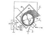
(6)磁気ブラシ帯電装置(図1及び図4):
図4は磁気ブラシ帯電装置2の拡大横断面模型図である。本実施の形態の磁気ブラシ帯電装置2は、大きく分けて、磁気ブラシ帯電部材(磁気ブラシ帯電器)2A、該磁気ブラシ帯電器2Aと導電性磁性粒子(帯電キャリア)14を収容させた容器(ハウジング)2、磁気ブラシ帯電器2Aに対する帯電バイアス印加電源E4等から成る。
The toner concentration (mixing ratio with the developing carrier c) of the developer 4f (t + c) in the developing container 4a is consumed successively as the toner is consumed for developing the electrostatic latent image. When the toner concentration of the developer 4f in the developing container 4a is detected by a detection unit (not shown) and decreases to a predetermined allowable lower limit concentration, the toner t is supplied from the toner supply unit 4g to the developer 4f in the developing container 4a. Thus, toner replenishment control is performed so that the toner concentration of the developer 4f in the developing container 4a is always kept within a predetermined allowable range.
(6) Magnetic brush charging device (FIGS. 1 and 4):
FIG. 4 is an enlarged cross-sectional model view of the magnetic
磁気ブラシ帯電器2Aは本実施の形態のものはスリーブ回転タイプであり、マグネットロール(磁石)12とこのマグネットロールに外嵌させた非磁性ステンレス製スリーブ(電極スリーブ、導電スリーブ、帯電スリーブ等と称される)13と、該スリーブ13の外周面にスリーブ内部のマグネットロール12の磁気力で磁気拘束させて形成保持させた磁性粒子14の磁気ブラシ部から成る。
The
マグネットロール12は、非回転の固定部材であり、スリーブ13はこのマグネットロール12の外回りを矢印bの方向に不図示の駆動系により所定の周速度、本実施の形態では225mm/secの周速で回転駆動される。又、スリーブ13は、感光対ドラム1に対してスペーサーコロ等の手段で500μm程度の隙間を保たせて配設してある。
The
2eは容器2に取り付けた、非磁性ステンレス製の磁気ブラシ層厚規制ブレードであり、スリーブ2b表面とのギャップが900μmになるように配置されている。容器2B内の磁性粒子14は、その一部がスリーブ13の外周面にスリーブ内部のマグネットロール12の磁気力で磁気拘束されて磁気ブラシ部2cとして保持される。磁気ブラシ部2は、スリーブ13の回転駆動に伴い、スリーブ13と一緒にスリーブ13と同方向に回転する。このとき、磁気ブラシ部の層厚はブレード15により均一厚さに規制させる。そして、その磁気ブラシ部の規制層厚はスリーブ13と感光体ドラム1との対向隙間部の間隔より大きいから、磁気ブラシ部はスリーブ13と感光対ドラム1との対向部において感光体ドラム1に対して所定幅のニップ部を形成して接触する。この接触ニップ部が帯電ニップ部Nである。
2e is a magnetic brush layer thickness regulating blade made of non-magnetic stainless steel attached to the
従って、回転感光体ドラム1は帯電ニップ部Nにおいて磁気ブラシ帯電器2Aのスリーブ13の回転に伴い回転する磁気ブラシ部で摺擦される。この場合、帯電ニップ部Nにおいて感光体ドラム1の移動方向と磁気ブラシ部の移動方向は逆方向となり、相対移動速度は速くなる。スリーブ13と磁気ブラシ層厚規制ブレード15には電源E4から所定の帯電バイアスが印加される。
Accordingly, the rotating
而して、感光体ドラム1が回転駆動され、磁気ブラシ帯電器2Aのスリーブ13が回転駆動され、電源E4から所定の帯電バイアスが印加されることで、回転感光体ドラム1の周面が本実施例の場合は注入帯電方式で所定の極製・電位に一様に接触帯電処理される。スリーブ13内に固定配置されているマグネットロール12は、スリーブ13と感光体ドラム1の最近接位置cとの角度θを感光ドラム回転方向上流側20°から下流側10°の範囲に入るようにすることが望ましく、上流側15°〜0°であれば更に良い。それより下流だと主極位置に磁性粒子が引き付けられ、帯電ニップ部Nの感光体ドラム回転方向下流側に磁性粒子の滞留が発生し易くなり、又、上流過ぎると、帯電ニップNを通過した磁性粒子の搬送性が悪くなり、滞留が発生し易くなる。又、帯電ニップ部Nに磁極がない場合は、磁性粒子に働くスリーブ13への拘束力が弱くなり、磁性粒子が感光体ドラム1に付着し易くなるのは明らかである。ここで述べている帯電ニップ部Nは、帯電時に磁性ブラシ部の磁性粒子が感光体ドラム1と接触している領域を示す。本実施の形態では、上流側10°の位置に約900Gの磁極を配置した。
Thus, the
磁気ブラシ部を構成させる磁性粒子14は、本実施の形態では、焼結した強磁性体(フェライト)を還元処理をしたものを用いたが、他に樹脂と強磁性体粉を混練して粒子状に成形したもの、若しくはこれに抵抗値調節のために導電性カーボン等を混ぜたものや、表面処理を行ったものも同様に用いることができる。磁気ブラシ部の磁性粒子14は、感光体ドラム表面のトラップ準位に電荷を良好に注入する役割と、感光体上ドラム上に生じたピンホール等の欠陥に帯電電流が集中してしまうことに起因して生じる帯電部材及び感光体の通電破壊を防止する役割を兼ね備えていなければならない。従って、磁気ブラシ帯電器2Aの電気抵抗値は1×10⁴Ω〜1×10⁹Ωであることが好ましく、特には1×10⁴Ω〜1×10⁷Ωであることが好ましい。磁気ブラシ帯電器2Aの電気抵抗値が1×10⁴Ω未満ではピンホールリークが生じ易くなる傾向があり、1×10⁹Ωを超えると良好な電荷の注入がしにくくなる傾向にある。又、抵抗値を抵抗値を上記範囲内に制御するためには、磁性粒子2dの体積抵抗値は1×10⁴Ω・cm〜1×10⁹Ω・cmであることが望ましく、特には1×10⁴Ω・cm〜1×107Ω・cmであることがより好ましい。
In this embodiment, the magnetic particles 14 constituting the magnetic brush portion are obtained by reducing the sintered ferromagnetic material (ferrite), but the particles are also obtained by kneading resin and ferromagnetic powder. The one formed into a shape, or the one mixed with conductive carbon or the like for adjusting the resistance value, or the one subjected to the surface treatment can be similarly used. The magnetic particles 14 of the magnetic brush portion have a role of favorably injecting charges into the trap level on the surface of the photosensitive drum, and that the charging current is concentrated on defects such as pinholes generated on the drum on the photosensitive drum. It must also have a role of preventing the energization destruction of the charging member and the photosensitive member caused by the cause. Therefore, the electric resistance value of the
本実施の形態で用いた磁気ブラシ帯電器2Aの電気抵抗値は、1×10⁶Ω・cmであり、帯電バイアスのDC成分として−700Vを印加することで、感光体ドラム1の表面電位も−700Vとなった。
The electric resistance value of the
磁性粒子14の体積抵抗値は、図6に略図を示す装置で測定した。即ち、セルAに磁性体粒子2dを充填し、該充填磁性体粒子14に接するように主電極17及び上部電極18を配し、該電極17,18間に定電圧電源22から電圧を印加し、そのとき流れる電流を電流計20で測定することにより求めた。19は絶縁物、21は電圧計、24はガイドリングを示す。その測定条件は、23℃、65%の環境で充填磁性粒子2dのセルとの接触面積S=2cm2、厚みd=1mm、上部電極18の荷重10kg、印加電圧100Vである
磁性粒子14の平均粒径及び粒度分布測定におけるピークは5〜100μmの範囲にあることが、粒子表面の汚染による帯電劣化防止及び磁性粒子の感光体ドラム1表面への付着防止の観点から好ましい。磁性粒子14の平均粒径は、水平方向最大弦長で示し、測定法は顕微鏡法により磁性粒子300個以上をランダムに選び、その径を実測して算術平均を取る。
The volume resistance value of the magnetic particles 14 was measured with an apparatus schematically shown in FIG. That is, the cell A is filled with the magnetic particles 2 d, the main electrode 17 and the
帯電バイアスは電源E2によってスリーブ13と規制ブレード15に印加される。本実施の形態では、DC成分にAC成分が重畳しているバイアスを用いている。 The charging bias is applied to the sleeve 13 and the regulating blade 15 by the power source E2. In this embodiment, a bias in which an AC component is superimposed on a DC component is used.
帯電ニップ部Nにおける、磁気ブラシ帯電器2Aの磁気ブラシ部による感光体ドラム1面の摺擦と、磁気ブラシ帯電器2Aへの帯電バイアスの印加により、磁気ブラシ部を構成している帯電用事製粒子14から電荷が感光体ドラム1上に与えられ、感光体ドラム1面が所定の極性・電位に一様に接触帯電される。本例の場合は前述したように、感光体ドラム1はその表面に電荷注入層を具備させたものであるから、電荷注入帯電により感光体ドラム1の帯電処理がなされる。即ち、感光ドラム1面が帯電バイアスDC+ACのDC成分に対応した電位に帯電される。スリーブ13は回転速度が速いほど帯電均一性が良好になる傾向にある。
In the charging nip portion N, the surface of the
磁気ブラシ帯電器2Aによる感光体ドラム1の電荷注入帯電は、図5の等価回路に示すような、抵抗RとコンデンサーCの直列回路と見なすことができる。このような回路の場合、抵抗値をr、感光体の静電容量をCp 、印加電圧をV0、帯電時間(感光体ドラム表面のある点が帯電ニップ部Nを通過する時間)をT0とすると、感光体ドラムの表面電位Vd は式(1)で表わされる。
The charge injection charging of the
Vd =V0(1−exp(T0/(Cp ・r)))・・・式(1)
帯電バイアスDC+ACにおいて、DC成分は必要とされる感光体ドラム1の表面電位と同値、本実施の形態では−700Vとした。
Vd = V0 (1-exp (T0 / (Cp · r))) Equation (1)
In the charging bias DC + AC, the DC component is set to the same value as the required surface potential of the
画像形成時(作像時)におけるAC成分は、そのピーク間電圧が小さい場合、帯電均一性、電位収束性の効果が薄く、大き過ぎる場合では、磁性粒子の滞留や感光体ドラムへの付着レベルが悪化する。又、そのVppの上下限は、通紙耐久継続時には、転写残トナーの混入量や、磁性粒子の劣化状態、或は外部の環境次第で変化する。即ち、トナー混入量が多い場合や、長期に亘る通紙耐久により磁性粒子にトナーや外添剤が付着して劣化した場合、外部環境が低湿度である場合、磁性粒子の抵抗値が上昇しているため適正な帯電を行うためにはVppを大きくし、電流量を増やすことが必要となる。 The AC component during image formation (image formation) has little effect on charging uniformity and potential convergence when the peak-to-peak voltage is small, and when it is too large, the retention of magnetic particles and the adhesion level to the photosensitive drum Gets worse. Further, the upper and lower limits of Vpp vary depending on the amount of toner remaining after transfer, the deterioration state of magnetic particles, or the external environment when the sheet passing durability is continued. That is, when the toner is mixed in a large amount, or when the toner is deteriorated due to adhesion of toner or external additives to the magnetic particles due to long-term paper passing durability, the resistance value of the magnetic particles increases when the external environment is low humidity. Therefore, in order to perform proper charging, it is necessary to increase Vpp and increase the amount of current.
しかしながら、Vppを大きくした場合の弊害として考えられる磁性粒子の感光体への付着レベルは逆に抵抗値が大きいほど減少する傾向にある。これは磁性粒子に注入される電荷量が大きいほど印加バイアスと感光体との電位差の影響を受け易く、より付着され易くなるためである。つまり、電流量に依存して、適正なACバイアス振幅は上下限共に同じ方向へシフトする。従って、逆に抵抗値が低い場合は磁性粒子の付着は増加する傾向にあるが、その分Vppを小さめに設定しても帯電には十分な電流量が得られる。 However, the adhesion level of the magnetic particles, which is considered to be harmful when Vpp is increased, tends to decrease as the resistance value increases. This is because the larger the amount of charge injected into the magnetic particles, the more easily affected by the potential difference between the applied bias and the photoreceptor, and the more easily attached. That is, depending on the amount of current, the proper AC bias amplitude shifts in the same direction for both upper and lower limits. Accordingly, when the resistance value is low, the adhesion of the magnetic particles tends to increase. However, even if Vpp is set smaller, a sufficient amount of current can be obtained for charging.
周波数は100Hz以上5000Hz以下、特に500Hz以上2000Hz以下が好ましい。それ以下では、磁性粒子の感光ドラムへの付着悪化や、帯電均一性、電位の立ち上がり性向上の効果が薄くなり、それ以上でも帯電均一性、電位の立ち上がり性向上の効果が得られにくくなる。ACの波形は矩形波、三角波、sin波等が良い。 The frequency is preferably 100 Hz to 5000 Hz, particularly preferably 500 Hz to 2000 Hz. Below that, the effect of improving the adhesion of magnetic particles to the photosensitive drum and improving the charging uniformity and potential rise properties become diminished, and the effect of improving the charging uniformity and potential rise properties becomes difficult to obtain even more. The AC waveform is preferably a rectangular wave, a triangular wave, a sin wave, or the like.
ここで、作像時、非作像時に帯電装置に印加するバイアスの特性について述べる。 Here, characteristics of the bias applied to the charging device during image formation and non-image formation will be described.
DC電界のみを帯電装置に印加した場合、帯電装置内に混入したトナーの感光体への吐き出し性は向上し、キャリアを劣化させず長時間維持するが、AC電界を印加した場合に比べ僅かのキャリア劣化に対しても帯電性は落ちる。例えば、帯電電位目標700Vに対し、初期、700V印加しても、690V程度にしか感光体上を帯電しない。磁気ブラシが耐久劣化してくると更に電位が低下し、AC電界を印加した場合との差が次第に広がってゆく。従って、現像バイアスのDC値に対して必要な逆電位が維持されず、かぶってしまうことになる。又、初期の設定電位に対し、電位低下が或る値を超えると露光部電位の変動により出力画像の初期に対する濃度変化が許容レベルを超えてしまうことになる。 When only the DC electric field is applied to the charging device, the discharge property of the toner mixed in the charging device to the photoreceptor is improved and the carrier is maintained for a long time without deteriorating, but is slightly smaller than when the AC electric field is applied. The chargeability also decreases with respect to carrier deterioration. For example, even if 700 V is initially applied to the charging potential target of 700 V, the photosensitive member is charged only to about 690 V. As the durability of the magnetic brush deteriorates, the potential further decreases, and the difference from the case where an AC electric field is applied gradually widens. Therefore, the reverse potential necessary for the DC value of the developing bias is not maintained, and the development bias is applied. Further, if the potential drop exceeds a certain value with respect to the initial set potential, the change in density of the output image exceeds the allowable level due to the fluctuation of the exposure portion potential.
通常かぶりだす電位低下レベルよりも、一定の濃度変化を引き起こす電位低下のレベルの方が条件としては厳しい。つまり、かぶらないまでも、帯電電位低下により現像コントラストが変化して出力画像の濃度及び色見が許容レベルを超えてしまうことがある。又、特にべた画像のような画像比率の高い画像が連続で出力された場合、一時的に帯電部材中のトナー濃度が上がって帯電能力が低下し、画像部ではゴーストが発生したり、必要な逆電位が維持されなくなるような事態も考えられるため、少なくとも紙が通過する通紙部はACバイアスを適正な振幅で印加し続けることが望ましい。 The level of the potential drop that causes a constant density change is more severe as a condition than the level of the potential drop that normally starts to appear. That is, even if it is not fogged, the development contrast may change due to a decrease in the charging potential, and the density and color appearance of the output image may exceed allowable levels. In particular, when an image with a high image ratio such as a solid image is output continuously, the toner density in the charging member temporarily increases and the charging ability decreases, and a ghost is generated in the image portion. Since there may be a situation where the reverse potential is not maintained, it is desirable to continue to apply the AC bias with an appropriate amplitude at least in the paper passing portion through which the paper passes.
このように、画像部は少なくとも安定したAC帯電を維持し、吐き出しは紙間及び前乃至後回転中に行うことが必要となる。しかしながら、紙間や後回転においてもかぶってしまうと紙間、後回転時の転写残トナーが発生し、帯電器混入トナー増加に繋がるため、かぶりの発生しない帯電レベルを維持することは必要である。その際、環境による帯電性、吐き出し性を考慮してバイアス設定をすることが望まれる。本実施の形態では、通常環境においては、印加バイアスの振幅を作像時は600V、非作像時は400Vと設定した。
(7)反転トナー吐き出し回収モード:
しかしながら、先述のようにドラム上、注入帯電器の磁気ブラシ内や現像機内に極性を殆ど持たないトナーや反転トナーが存在し、それが転写部に至った場合、厚紙やコート紙に圧力転写されてしまうという不具合がある。
As described above, the image portion is required to maintain at least stable AC charging, and the discharge needs to be performed between the sheets and during the front to rear rotation. However, if it is covered even between papers or after rotation, transfer residual toner is generated between papers and after rotation, which leads to an increase in toner mixed in the charger. Therefore, it is necessary to maintain a charge level at which fog does not occur. . At that time, it is desirable to set the bias in consideration of the charging property and discharging property depending on the environment. In the present embodiment, in a normal environment, the amplitude of the applied bias is set to 600 V during image formation and 400 V during non-image formation.
(7) Reverse toner discharge recovery mode:
However, as described above, there is toner having no polarity or reversal toner on the drum, in the magnetic brush of the charging charger or in the developing machine, and when it reaches the transfer section, it is pressure transferred to cardboard or coated paper. There is a problem that it ends up.
ドラム上に存在する極性を持たないトナーや反転トナーは、通常転写バイアスや現像バイアスの作用により除去される機会が少ないため、注入帯電器の磁気ブラシ内部に蓄積することが多い。注入帯電器からドラム上に吐き出されるトナーは、この反転トナーと正規極性トナーが共に存在する。正規極性トナーは、非画像領域においては現像部で回収されるため、画像に影響を与えることは少なく、又、非作像時の吐き出しバイアスにより常に処理されている。 Non-polar toner and reversal toner present on the drum are usually accumulated in the magnetic brush of the injection charger because there are few opportunities to be removed by the action of transfer bias and development bias. The toner discharged from the injection charger onto the drum includes both the reversal toner and the normal polarity toner. The normal polarity toner is collected by the developing unit in the non-image area, and therefore has little influence on the image, and is always processed by the discharge bias during non-image formation.
一方、反転トナーが作像時に吐き出された場合には、現像部で回収されないため、厚紙やコート紙ではかぶりが発生してしまう。これは、極微量の反転トナーが存在するだけでも発生してしまうことが分かった。そのため、厚紙やコート紙を使用する場合においては、反転トナーについても処理する機構を設ける必要がある。厚紙使用がごく稀である場合は、作像時に反転トナーが吐き出されないようなバイアス設定も可能ではある。 On the other hand, when the reversal toner is discharged at the time of image formation, it is not collected by the developing unit, and thus fogging occurs on thick paper or coated paper. It has been found that this occurs even when a very small amount of reversal toner is present. Therefore, when using thick paper or coated paper, it is necessary to provide a mechanism for processing reversal toner. When the use of cardboard is rare, it is possible to set a bias so that the reverse toner is not discharged during image formation.
しかし、厚紙が頻繁に使用される場合は反転トナーはバイアスの設定に対し、正規トナーとは正反対の挙動を示すため、上述の正規トナーの処理のためのバイアス設定とは両立できない。従って、予め帯電器内に混入している反転トナーを特別に軽減しておく必要がある。 However, when thick paper is frequently used, the reversal toner exhibits a behavior opposite to that of the normal toner with respect to the bias setting, and thus cannot be compatible with the above-described bias setting for processing the normal toner. Therefore, it is necessary to reduce the reversal toner mixed in the charger in advance.
そこで、本実施の形態では、A4サイズの通紙100枚ごとに、100枚目の排紙後、5秒間の反転トナー吐き出し回収モードを設定した。以下に詳細を説明する。 Therefore, in the present embodiment, the reverse toner discharge / collection mode for 5 seconds is set for every 100 A4 size sheets after the 100th sheet is discharged. Details will be described below.
このモード時における帯電バイアスのAC振幅は、作像時より高い750Vとした。これは、反転トナーはΔVが小さければ小さいほど良く、帯電電位の収束性をより高めたものである。この設定によって蓄積されていた反転トナーが吐き出される。 The AC amplitude of the charging bias in this mode was set to 750 V, which is higher than that at the time of image formation. This is because the reversal toner is better as ΔV is smaller, and the convergence of the charged potential is further improved. The reverse toner accumulated by this setting is discharged.
次に、現像器における回収は、現像バイアスを帯電電位により近付けることにより回収する。具体的には、帯電電位が−700Vであり、通常設定では現像バイアスは−500Vという設定であるのに対し、本モードでは−650Vにする。このことにより、正規のネガ極性トナーが電界の作用で現像装置から感光体に付着することもあるが、それらは通常の通紙モードで再回収可能であり、それよりもこれまで回収されることのなかった反転トナーが現像バイアスのAC成分により感光体から離され、最終的に2成分現像器の磁性粒子の穂に掻き取られて回収されることとなった効果は大きい。 Next, the recovery in the developing device is performed by bringing the developing bias closer to the charging potential. Specifically, the charging potential is −700 V, and in the normal setting, the developing bias is set to −500 V, whereas in this mode, it is set to −650 V. As a result, regular negative polarity toner may adhere to the photoconductor from the developing device due to the action of an electric field, but they can be collected again in the normal paper-passing mode and are collected more than before. The reversal toner without toner is separated from the photosensitive member by the AC component of the developing bias, and is finally scraped off and collected by the magnetic particle ears of the two-component developing device.
<実施の形態2>
次に、本発明における実施の形態2について説明する。
<
Next, a second embodiment of the present invention will be described.
本実施の形態においては、実施の形態1と同様の磁気ブラシ注入帯電方式を用いたクリーナレスシステムを採用しており、帯電装置上流に配置した補助帯電ブラシに印加するバイアスを同時に制御することにより、反転トナーの吐き出し性を向上させている。 In the present embodiment, a cleanerless system using the magnetic brush injection charging method similar to that of the first embodiment is adopted, and by simultaneously controlling the bias applied to the auxiliary charging brush arranged upstream of the charging device. Thus, the reversal toner discharge performance is improved.
前述のように、図1中、12は転写装置5と磁気ブラシ帯電装置2との間において感光ドラムに当接させ、ACバイアス、帯電と逆極性のDCバイアス、又はACバイアスを重畳した帯電と逆極性のDCバイアスを印加した導電性ブラシであり、磁気ブラシ帯電装置2による帯電直前の感光体ドラム表面電位をならすと同時に、転写残トナーを除電、若しくは感光体ドラムの帯電と逆極性に帯電して、磁気ブラシ帯電器2Aの磁気ブラシ部での回収を容易にする。常温常湿環境下ではプラス500V程度のDCバイアスを印加し、環境によりその値を制御する構成を採っている。
As described above, in FIG. 1,
ここで、磁気ブラシに混入した極性を持たないトナーや反転トナーは帯電バイアスのAC成分(交流成分)の振幅Vppを大きくし、電位差ΔVを小さくすることで吐き出すことが可能であったが、該補助ブラシには常時帯電極性とは逆極性のバイアスを印加していたため、磁気ブラシによる帯電後においても、ブラシの毛先通過部など逆電荷が特に注入される微小領域で帯電不良部が残ってしまうことがある。つまり、その領域でΔVが或る値を持つということを意味し、反転トナーが吐き出されにくい状態であると言える。 Here, non-polar toner or reversal toner mixed in the magnetic brush could be discharged by increasing the amplitude Vpp of the AC component (AC component) of the charging bias and decreasing the potential difference ΔV. Since a bias having a polarity opposite to the charging polarity is always applied to the auxiliary brush, even after charging by the magnetic brush, a poorly charged portion remains in a minute region where the reverse charge is injected, such as a brush tip passage portion. It may end up. That is, it means that ΔV has a certain value in that region, and it can be said that the reverse toner is not easily discharged.
そこで、本実施の形態では実施の形態1における反転トナー吐き出し回収モードにおいて、補助ブラシ印加バイアスにマイナス1000VのDCバイアスを印加した。このとき、補助ブラシ通過後のドラム表面電位は−800V程度まで帯電しており、本来の磁気ブラシ帯電の帯電DCバイアスよりも帯電極性側に高い値となる。このとき、帯電電位は磁気ブラシ帯電通過後は磁気ブラシに印加するACバイアスにより−700Vに収束するため、帯電電位の制御になんら支障はない。反転トナーの吐き出し性は、ΔVが残らず、むしろマイナスになる部分が生じるために向上する。 Therefore, in the present embodiment, a DC bias of minus 1000 V is applied to the auxiliary brush application bias in the reverse toner discharge recovery mode in the first embodiment. At this time, the drum surface potential after passing through the auxiliary brush is charged to about −800 V, which is higher on the charging polarity side than the charging DC bias of the original magnetic brush charging. At this time, the charged potential converges to −700 V by the AC bias applied to the magnetic brush after passing through the charging of the magnetic brush, so there is no problem in controlling the charging potential. The dischargeability of the reversal toner is improved because ΔV does not remain but rather a negative portion occurs.
<実施の形態3>
本実施の形態は、本発明を帯電ローラを用いたクリーナレスシステムに適用した場合を示す。図1は本実施の形態におけるドラム周りの構成図である。
<Embodiment 3>
In the present embodiment, the present invention is applied to a cleanerless system using a charging roller. FIG. 1 is a configuration diagram around a drum in the present embodiment.
2は帯電ローラ、4は現像装置、5aは転写ローラである。7に示す補助ブラシAには、動作中は−800VのDCバイアスが印加され、8に示す補助ブラシBには+400VのDCバイアスが印加されている。補助ブラシBは、転写後のドラム表面電位の履歴を消去するために帯電極性と逆極性のバイアスが印加されており、補助ブラシAは、転写残トナーの帯電電荷を一様に正規極性、即ちマイナスに揃える効果及び帯電の補助的な機能を持つものである。 2 is a charging roller, 4 is a developing device, and 5a is a transfer roller. A DC bias of −800 V is applied to the auxiliary brush A shown in 7 during operation, and a DC bias of +400 V is applied to the auxiliary brush B shown in 8. The auxiliary brush B is applied with a bias having a polarity opposite to the charging polarity in order to erase the history of the drum surface potential after the transfer, and the auxiliary brush A uniformly applies the charged charge of the transfer residual toner to the normal polarity, that is, It has a negative effect and an auxiliary charging function.
一方、帯電ローラ2には通常環境では−700VのDCバイアスに、2000μAの交流電流を維持する一定電流制御を施した交流バイアスを重畳している。補助ブラシAを通過してくる転写残トナーは理想的にはマイナス極性を持つものであり、帯電ローラ5通過時に受けるAC放電により、現像回収に適した−30μC/cm2程度に収束するが、一部帯電ローラに付着し、帯電不良の原因となる。この帯電ローラに付着するトナーは反転トナーが多く、適宜感光体へ戻していくことが望ましい。
On the other hand, in a normal environment, the charging
そこで、本実施の形態においては、実施の形態2のように反転トナー吐き出し回収モードを設けた。吐き出し回収モード時の高圧設定は、補助ブラシBはOFF、補助ブラシAは−1000V、帯電ローラは通常通りである。 Therefore, in the present embodiment, a reverse toner discharge recovery mode is provided as in the second embodiment. The high pressure setting in the discharge recovery mode is OFF for the auxiliary brush B, -1000 V for the auxiliary brush A, and normal charging roller.
反転トナー吐き出し回収モード時における現像バイアスは、DCバイアスを−650Vとすることは前記実施の形態1,2と同様とし、AC成分の振幅を1.8kVから2.2kVに変更した。通常は現像コントラストに対する現像トナー量のリニアリティを確保するために最適な振幅を設定するが、このトナー回収だけを目的とした間は、極力高い振幅で回収性を高めることが望ましい。
ぶりを長期に亘って効果的に防止することができた。又、反転トナーが帯電機内に混入している影響である帯電器からの飛散や、帯電不良の発生をより長期に亘って防止することができた。
As for the developing bias in the reverse toner discharge and recovery mode, the DC bias is set to −650 V as in the first and second embodiments, and the AC component amplitude is changed from 1.8 kV to 2.2 kV. Normally, an optimal amplitude is set to ensure the linearity of the developing toner amount with respect to the developing contrast, but it is desirable to improve the recoverability with as high an amplitude as possible while aiming only at this toner recovery.
The fog could be effectively prevented over a long period of time. In addition, scattering from the charger and the occurrence of charging failure, which are the effects of reversal toner mixed in the charger, can be prevented for a longer period.
本発明は特に、磁気ブラシ注入帯電装置を例に説明がなされたが、その他の各種帯電装置にも適用でき、又、高圧条件も、DC成分や、周波数、波形等、あらゆる代替が可能であることは明白である。 The present invention has been particularly described with reference to a magnetic brush injection charging device. However, the present invention can be applied to other various charging devices, and the high voltage condition can be replaced with any DC component, frequency, waveform, etc. It is obvious.
1 感光ドラム
2 磁気ブラシ帯電装置
3 レーザービームスキャナ
4 現像装置
5 転写装置
6 給紙カセット
7 給紙ローラ
8 搬送ローラ
9,10 シートパス
11 定着装置
12 導電性ブラシ
14 磁気ブラシ部
DESCRIPTION OF
Claims (18)
正規の極性とは逆の極性の電荷を帯びた現像剤を前記現像装置で回収する手段を有することを特徴とする画像形成装置。 A developer charged on a developer carrying member is formed by applying a bias voltage to a charging member facing the member to be charged to charge the member to be charged, and performing image exposure by an image exposure unit to form a latent image. And developing means for developing the latent image to form a toner image, and an image forming apparatus that also serves as a cleaning means for collecting residual toner particles remaining on the image carrier after the developing means transfers the toner image to a transfer material In
An image forming apparatus comprising: a developer that collects a developer having a charge opposite to a normal polarity by the developing device.
Priority Applications (1)
| Application Number | Priority Date | Filing Date | Title |
|---|---|---|---|
| JP2004151685A JP2005331822A (en) | 2004-05-21 | 2004-05-21 | Image forming apparatus |
Applications Claiming Priority (1)
| Application Number | Priority Date | Filing Date | Title |
|---|---|---|---|
| JP2004151685A JP2005331822A (en) | 2004-05-21 | 2004-05-21 | Image forming apparatus |
Publications (1)
| Publication Number | Publication Date |
|---|---|
| JP2005331822A true JP2005331822A (en) | 2005-12-02 |
Family
ID=35486518
Family Applications (1)
| Application Number | Title | Priority Date | Filing Date |
|---|---|---|---|
| JP2004151685A Withdrawn JP2005331822A (en) | 2004-05-21 | 2004-05-21 | Image forming apparatus |
Country Status (1)
| Country | Link |
|---|---|
| JP (1) | JP2005331822A (en) |
Cited By (1)
| Publication number | Priority date | Publication date | Assignee | Title |
|---|---|---|---|---|
| US8153342B2 (en) | 2006-09-19 | 2012-04-10 | Ricoh Company, Ltd. | Developer, and image forming apparatus and image forming method using the developer |
-
2004
- 2004-05-21 JP JP2004151685A patent/JP2005331822A/en not_active Withdrawn
Cited By (1)
| Publication number | Priority date | Publication date | Assignee | Title |
|---|---|---|---|---|
| US8153342B2 (en) | 2006-09-19 | 2012-04-10 | Ricoh Company, Ltd. | Developer, and image forming apparatus and image forming method using the developer |
Similar Documents
| Publication | Publication Date | Title |
|---|---|---|
| JP3768800B2 (en) | Image forming apparatus | |
| JP3780136B2 (en) | Image forming apparatus | |
| CN100394317C (en) | image forming device | |
| US6144824A (en) | Image forming method for preventing an uneven potential of an image bearing member having a charge injecting layer | |
| JP2000081772A (en) | Image forming device | |
| JP3466956B2 (en) | Image forming device | |
| JP2003280335A (en) | Image forming device | |
| JP2004045570A (en) | Image forming device | |
| JP2003241511A (en) | Image forming device | |
| JP4261741B2 (en) | Image forming apparatus | |
| JP2000284570A (en) | Image forming device | |
| JP2005165114A (en) | Image forming apparatus | |
| JP4422858B2 (en) | Image forming apparatus | |
| JP2005331822A (en) | Image forming apparatus | |
| JP4323688B2 (en) | Image forming apparatus | |
| JP2001350323A (en) | Image forming device | |
| JP2000293083A (en) | Image forming device | |
| JP2004252180A (en) | Image forming device | |
| JP2003295584A (en) | Image forming device | |
| JP4617003B2 (en) | Image forming apparatus | |
| JP2004077971A (en) | Image forming device | |
| JP2000314993A (en) | Image forming device | |
| JP2000293015A (en) | Image forming device | |
| JP2003280456A (en) | Image forming device | |
| JP2001343866A (en) | Image forming device |
Legal Events
| Date | Code | Title | Description |
|---|---|---|---|
| RD01 | Notification of change of attorney |
Free format text: JAPANESE INTERMEDIATE CODE: A7421 Effective date: 20060201 |
|
| A300 | Withdrawal of application because of no request for examination |
Free format text: JAPANESE INTERMEDIATE CODE: A300 Effective date: 20070807 |