JP2005311014A - Niobium solid electrolytic capacitor - Google Patents
Niobium solid electrolytic capacitor Download PDFInfo
- Publication number
- JP2005311014A JP2005311014A JP2004125135A JP2004125135A JP2005311014A JP 2005311014 A JP2005311014 A JP 2005311014A JP 2004125135 A JP2004125135 A JP 2004125135A JP 2004125135 A JP2004125135 A JP 2004125135A JP 2005311014 A JP2005311014 A JP 2005311014A
- Authority
- JP
- Japan
- Prior art keywords
- capacitor
- anode
- niobium
- terminal
- cathode
- Prior art date
- Legal status (The legal status is an assumption and is not a legal conclusion. Google has not performed a legal analysis and makes no representation as to the accuracy of the status listed.)
- Pending
Links
- 239000003990 capacitor Substances 0.000 title claims abstract description 112
- GUCVJGMIXFAOAE-UHFFFAOYSA-N niobium atom Chemical compound [Nb] GUCVJGMIXFAOAE-UHFFFAOYSA-N 0.000 title claims abstract description 51
- 229910052758 niobium Inorganic materials 0.000 title claims abstract description 40
- 239000010955 niobium Substances 0.000 title claims abstract description 40
- 239000007787 solid Substances 0.000 title claims abstract description 34
- 239000011347 resin Substances 0.000 claims abstract description 35
- 229920005989 resin Polymers 0.000 claims abstract description 35
- 238000000465 moulding Methods 0.000 claims abstract 3
- 229910052751 metal Inorganic materials 0.000 claims description 41
- 239000002184 metal Substances 0.000 claims description 41
- OKTJSMMVPCPJKN-UHFFFAOYSA-N Carbon Chemical compound [C] OKTJSMMVPCPJKN-UHFFFAOYSA-N 0.000 claims description 16
- 229910052799 carbon Inorganic materials 0.000 claims description 16
- 239000000843 powder Substances 0.000 claims description 12
- 150000002822 niobium compounds Chemical class 0.000 claims description 6
- 239000011248 coating agent Substances 0.000 abstract description 2
- 238000000576 coating method Methods 0.000 abstract description 2
- 238000004904 shortening Methods 0.000 abstract 1
- 230000000052 comparative effect Effects 0.000 description 17
- 239000000853 adhesive Substances 0.000 description 13
- 230000001070 adhesive effect Effects 0.000 description 13
- BQCADISMDOOEFD-UHFFFAOYSA-N Silver Chemical compound [Ag] BQCADISMDOOEFD-UHFFFAOYSA-N 0.000 description 11
- 239000010408 film Substances 0.000 description 11
- 238000000034 method Methods 0.000 description 11
- 229910052709 silver Inorganic materials 0.000 description 8
- 239000004332 silver Substances 0.000 description 8
- NBIIXXVUZAFLBC-UHFFFAOYSA-N Phosphoric acid Chemical compound OP(O)(O)=O NBIIXXVUZAFLBC-UHFFFAOYSA-N 0.000 description 6
- 238000001746 injection moulding Methods 0.000 description 6
- GUVRBAGPIYLISA-UHFFFAOYSA-N tantalum atom Chemical compound [Ta] GUVRBAGPIYLISA-UHFFFAOYSA-N 0.000 description 6
- 239000010409 thin film Substances 0.000 description 6
- 238000003466 welding Methods 0.000 description 5
- VZSRBBMJRBPUNF-UHFFFAOYSA-N 2-(2,3-dihydro-1H-inden-2-ylamino)-N-[3-oxo-3-(2,4,6,7-tetrahydrotriazolo[4,5-c]pyridin-5-yl)propyl]pyrimidine-5-carboxamide Chemical compound C1C(CC2=CC=CC=C12)NC1=NC=C(C=N1)C(=O)NCCC(N1CC2=C(CC1)NN=N2)=O VZSRBBMJRBPUNF-UHFFFAOYSA-N 0.000 description 4
- 230000000694 effects Effects 0.000 description 4
- NUJOXMJBOLGQSY-UHFFFAOYSA-N manganese dioxide Chemical compound O=[Mn]=O NUJOXMJBOLGQSY-UHFFFAOYSA-N 0.000 description 4
- 239000000463 material Substances 0.000 description 4
- 238000005245 sintering Methods 0.000 description 4
- 239000007784 solid electrolyte Substances 0.000 description 4
- 229910052715 tantalum Inorganic materials 0.000 description 4
- AFCARXCZXQIEQB-UHFFFAOYSA-N N-[3-oxo-3-(2,4,6,7-tetrahydrotriazolo[4,5-c]pyridin-5-yl)propyl]-2-[[3-(trifluoromethoxy)phenyl]methylamino]pyrimidine-5-carboxamide Chemical compound O=C(CCNC(=O)C=1C=NC(=NC=1)NCC1=CC(=CC=C1)OC(F)(F)F)N1CC2=C(CC1)NN=N2 AFCARXCZXQIEQB-UHFFFAOYSA-N 0.000 description 3
- 229910000147 aluminium phosphate Inorganic materials 0.000 description 3
- 239000007864 aqueous solution Substances 0.000 description 3
- 229920001940 conductive polymer Polymers 0.000 description 3
- 239000011148 porous material Substances 0.000 description 3
- HMUNWXXNJPVALC-UHFFFAOYSA-N 1-[4-[2-(2,3-dihydro-1H-inden-2-ylamino)pyrimidin-5-yl]piperazin-1-yl]-2-(2,4,6,7-tetrahydrotriazolo[4,5-c]pyridin-5-yl)ethanone Chemical compound C1C(CC2=CC=CC=C12)NC1=NC=C(C=N1)N1CCN(CC1)C(CN1CC2=C(CC1)NN=N2)=O HMUNWXXNJPVALC-UHFFFAOYSA-N 0.000 description 2
- NLZUEZXRPGMBCV-UHFFFAOYSA-N Butylhydroxytoluene Chemical compound CC1=CC(C(C)(C)C)=C(O)C(C(C)(C)C)=C1 NLZUEZXRPGMBCV-UHFFFAOYSA-N 0.000 description 2
- 229910010272 inorganic material Inorganic materials 0.000 description 2
- 239000011147 inorganic material Substances 0.000 description 2
- 238000004898 kneading Methods 0.000 description 2
- 229910000484 niobium oxide Inorganic materials 0.000 description 2
- URLJKFSTXLNXLG-UHFFFAOYSA-N niobium(5+);oxygen(2-) Chemical compound [O-2].[O-2].[O-2].[O-2].[O-2].[Nb+5].[Nb+5] URLJKFSTXLNXLG-UHFFFAOYSA-N 0.000 description 2
- 239000011368 organic material Substances 0.000 description 2
- 229920000128 polypyrrole Polymers 0.000 description 2
- 150000003839 salts Chemical class 0.000 description 2
- 239000000725 suspension Substances 0.000 description 2
- XLYOFNOQVPJJNP-UHFFFAOYSA-N water Substances O XLYOFNOQVPJJNP-UHFFFAOYSA-N 0.000 description 2
- YLZOPXRUQYQQID-UHFFFAOYSA-N 3-(2,4,6,7-tetrahydrotriazolo[4,5-c]pyridin-5-yl)-1-[4-[2-[[3-(trifluoromethoxy)phenyl]methylamino]pyrimidin-5-yl]piperazin-1-yl]propan-1-one Chemical compound N1N=NC=2CN(CCC=21)CCC(=O)N1CCN(CC1)C=1C=NC(=NC=1)NCC1=CC(=CC=C1)OC(F)(F)F YLZOPXRUQYQQID-UHFFFAOYSA-N 0.000 description 1
- RYGMFSIKBFXOCR-UHFFFAOYSA-N Copper Chemical compound [Cu] RYGMFSIKBFXOCR-UHFFFAOYSA-N 0.000 description 1
- NIPNSKYNPDTRPC-UHFFFAOYSA-N N-[2-oxo-2-(2,4,6,7-tetrahydrotriazolo[4,5-c]pyridin-5-yl)ethyl]-2-[[3-(trifluoromethoxy)phenyl]methylamino]pyrimidine-5-carboxamide Chemical compound O=C(CNC(=O)C=1C=NC(=NC=1)NCC1=CC(=CC=C1)OC(F)(F)F)N1CC2=C(CC1)NN=N2 NIPNSKYNPDTRPC-UHFFFAOYSA-N 0.000 description 1
- 230000032683 aging Effects 0.000 description 1
- 229910052782 aluminium Inorganic materials 0.000 description 1
- XAGFODPZIPBFFR-UHFFFAOYSA-N aluminium Chemical compound [Al] XAGFODPZIPBFFR-UHFFFAOYSA-N 0.000 description 1
- CFJRGWXELQQLSA-UHFFFAOYSA-N azanylidyneniobium Chemical compound [Nb]#N CFJRGWXELQQLSA-UHFFFAOYSA-N 0.000 description 1
- 238000005452 bending Methods 0.000 description 1
- 238000006243 chemical reaction Methods 0.000 description 1
- 239000004020 conductor Substances 0.000 description 1
- 229910052802 copper Inorganic materials 0.000 description 1
- 239000010949 copper Substances 0.000 description 1
- 150000002739 metals Chemical class 0.000 description 1
- 239000000203 mixture Substances 0.000 description 1
- 230000003647 oxidation Effects 0.000 description 1
- 238000007254 oxidation reaction Methods 0.000 description 1
- 239000000126 substance Substances 0.000 description 1
- 230000002195 synergetic effect Effects 0.000 description 1
Images




Classifications
-
- H—ELECTRICITY
- H01—ELECTRIC ELEMENTS
- H01G—CAPACITORS; CAPACITORS, RECTIFIERS, DETECTORS, SWITCHING DEVICES, LIGHT-SENSITIVE OR TEMPERATURE-SENSITIVE DEVICES OF THE ELECTROLYTIC TYPE
- H01G9/00—Electrolytic capacitors, rectifiers, detectors, switching devices, light-sensitive or temperature-sensitive devices; Processes of their manufacture
- H01G9/004—Details
- H01G9/008—Terminals
- H01G9/012—Terminals specially adapted for solid capacitors
-
- H—ELECTRICITY
- H01—ELECTRIC ELEMENTS
- H01G—CAPACITORS; CAPACITORS, RECTIFIERS, DETECTORS, SWITCHING DEVICES, LIGHT-SENSITIVE OR TEMPERATURE-SENSITIVE DEVICES OF THE ELECTROLYTIC TYPE
- H01G9/00—Electrolytic capacitors, rectifiers, detectors, switching devices, light-sensitive or temperature-sensitive devices; Processes of their manufacture
- H01G9/004—Details
- H01G9/14—Structural combinations or circuits for modifying, or compensating for, electric characteristics of electrolytic capacitors
Landscapes
- Engineering & Computer Science (AREA)
- Power Engineering (AREA)
- Microelectronics & Electronic Packaging (AREA)
- Fixed Capacitors And Capacitor Manufacturing Machines (AREA)
- Powder Metallurgy (AREA)
Abstract
Description
本発明は、ニオブ、又はニオブ化合物を主成分とする粉末焼結体を陽極体として用いるニオブ固体電解コンデンサに関する。 The present invention relates to a niobium solid electrolytic capacitor using a powder sintered body containing niobium or a niobium compound as a main component as an anode body.
タンタル、ニオブ、アルミニウム等の弁金属を用いた固体電解コンデンサとして図6に示すようなものが知られている。この固体電解コンデンサは、例えばタンタル粉末にタンタルからなる陽極リード部材(1a)を植立して焼結したものを陽極体(1)として、該陽極体(1)をリン酸等を含む水溶液中で陽極酸化(以下、化成という)して陽極体(1)表面に誘電体皮膜(2)を形成する。次いで、該誘電体皮膜(2)上に二酸化マンガン等の導電性無機材料、或いはTCNQ錯塩、導電性ポリマー等の導電性有機材料からなる陰極層(3)を形成し、カーボン層(4)、銀、銅等の金属を含む金属ペースト層(5)を順次形成してコンデンサ本体(15)を作製する。その後、陰極端子(21)の所定位置に導電性接着剤(8)として少量の銀ペーストを滴下し、その上から前記コンデンサ本体(15)を載置し、熱硬化して前記コンデンサ本体(15)と陰極端子(21)とを電気的に接続し、固定する。一方、陽極リード部材(1a)と陽極端子(20)とを溶接接続する。然る後、陽極端子(20)と陰極端子(21)とを外部に導出した形で前記コンデンサ本体(15)を例えば外装樹脂(7)等の射出成形により被覆密閉する。前記外部に導出した陽極端子(20)及び陰極端子(21)は、前記外装樹脂(7)に沿って折り曲げられて固体電解コンデンサが完成する (例えば、特許文献1) 。 A solid electrolytic capacitor using a valve metal such as tantalum, niobium, or aluminum is known as shown in FIG. In this solid electrolytic capacitor, for example, an anode lead member (1a) made of tantalum and planted with tantalum powder is sintered as an anode body (1), and the anode body (1) is in an aqueous solution containing phosphoric acid or the like. Then, a dielectric film (2) is formed on the surface of the anode body (1) by anodic oxidation (hereinafter referred to as chemical conversion). Next, a cathode layer (3) made of a conductive inorganic material such as manganese dioxide or a conductive organic material such as a TCNQ complex salt or a conductive polymer is formed on the dielectric film (2), and a carbon layer (4), A metal paste layer (5) containing a metal such as silver or copper is sequentially formed to produce a capacitor body (15). Thereafter, a small amount of silver paste is dropped as a conductive adhesive (8) on a predetermined position of the cathode terminal (21), and the capacitor body (15) is placed thereon, and is thermally cured to form the capacitor body (15 ) And the cathode terminal (21) are electrically connected and fixed. On the other hand, the anode lead member (1a) and the anode terminal (20) are connected by welding. Thereafter, the capacitor body (15) is covered and sealed by injection molding of, for example, an exterior resin (7) with the anode terminal (20) and the cathode terminal (21) led out to the outside. The anode terminal (20) and the cathode terminal (21) led out to the outside are bent along the exterior resin (7) to complete a solid electrolytic capacitor (for example, Patent Document 1).
近年、小型化が求められる一方でCPUの高速化、低電圧化、電圧変動平準化などの要求が高まり、コンデンサの大容量化、等価直列抵抗(以下、ESR) の低減が限りなく求められるようになってきた。コンデンサの容量と定格電圧の積(以下、CV積)を増大させるには、例えば素子を分厚くする方法が考えられるが、この場合誘電体皮膜から陰極引出層までの平均パスが長くなりESRが増大してしまう。即ち、リードフレームの比抵抗は金属なので数μ〜数十μ〔Ω・cm〕であるのに対し、固体電解コンデンサに実用されている固体電解質は数千μ〜数千m〔Ω・cm〕と非常に高いため固体電解質のパスの長さはコンデンサ性能上、重要な要因となる。この問題は、弁金属の中でも素子内に形成される粉末間の細孔(以下、ポア)の充分な太さ、均一性を確保することが困難なニオブ焼結体を用いる場合に特に問題になる。ニオブに比べ焼結力が弱く脆い酸化ニオブを陽極体として用いる場合、ニオブよりも3〜400℃高い温度で焼結するため、ポアがさらに細くなり前記問題が顕著になる(例えば、特許文献2)。
この問題の改善策として、図4に示すように金属ペースト層(5)まで形成した2つのコンデンサ本体(15)を重ねて用いる(以下、素子2分割化)ことにより誘電体皮膜(2)から金属ペースト層(5)までの平均パスを半減させる方法が実施されている。これは金属ペースト層(5)が金属に近い導電性をもつことから考え出された方法である。即ち、金属ペースト層(5)は銀等の金属粉(5a)と樹脂(5b)とを練ったものからなり、硬化後の金属ペースト層(5)の比抵抗を膜の長さ方向で測定した場合、数十μ〔Ω・cm〕で金属に近い導電性を示す。ところが、図5に示すように実際には、硬化の際に金属ペースト層(5)の表皮にはほとんど樹脂(5b)だけの薄膜が形成され、金属ペースト層(5)の厚さ方向の比抵抗は長さ方向の測定値に比べ著しく高い値になってしまう。上記のような素子2分割化の構造を用いた場合、表皮に樹脂(5b)だけの薄膜を導電性接着剤(8)により夫々接続したことになり、その結果平均パスの半減によるESR低減の効果を充分に得ることができないという問題がある。この問題は、燐片状又はフレーク状の金属粉(5a)を用いた場合に顕著になり、ESR増加の大きな原因になっている。 As a measure to solve this problem, as shown in FIG. 4, two capacitor bodies (15) formed up to the metal paste layer (5) are used in an overlapping manner (hereinafter, divided into two elements). A method of halving the average path to the metal paste layer (5) has been implemented. This is a method conceived from the fact that the metal paste layer (5) has conductivity close to that of metal. That is, the metal paste layer (5) consists of a kneaded metal powder (5a) such as silver and a resin (5b), and the specific resistance of the cured metal paste layer (5) is measured in the length direction of the film. In this case, the conductivity is close to that of metal at several tens of μ [Ω · cm]. However, as shown in FIG. 5, in actuality, a thin film of almost only resin (5b) is formed on the skin of the metal paste layer (5) during curing, and the ratio of the thickness direction of the metal paste layer (5) is reduced. The resistance is significantly higher than the measured value in the length direction. In the case of using the two-element structure as described above, a thin film of only the resin (5b) is connected to the outer skin by the conductive adhesive (8), and as a result, the ESR is reduced by halving the average path. There is a problem that the effect cannot be obtained sufficiently. This problem becomes prominent when the flake-like or flake-like metal powder (5a) is used, and is a major cause of an increase in ESR.
そこで、本発明は上記問題に鑑み、誘電体皮膜から陰極引出層までの平均パスを低減させ、コンデンサの大容量化してもESRの低いニオブ固体電解コンデンサを提供する。 In view of the above problems, the present invention provides a niobium solid electrolytic capacitor having a low ESR even when the average path from the dielectric film to the cathode lead layer is reduced and the capacity of the capacitor is increased.
本発明は、ニオブ又はニオブ化合物を主成分とする粉末焼結体からなる陽極体(1)に、陽極リード部材(1a)を具え、前記陽極体(1)の表面に誘電体皮膜(2)、陰極層(3)を形成したコンデンサ素子(10)に、カーボン層(4)、及び金属ペースト層(5)を形成してコンデンサ本体(15)を構成し、該コンデンサ本体(15)を2つ具えるニオブ固体電解コンデンサにおいて、コンデンサ本体(15)の夫々の陽極リード部材(1a)に電気的に接続された陽極端子(20)と、2つのコンデンサ本体(15)(15)に挟まれて電気的に接続された陰極端子(21)と、2つのコンデンサ本体(15)(15)、陽極端子(20)及び陰極端子(21)を被覆して、これらを一体モールドしてなる外装樹脂(7)とからなり、前記陽極端子(20)及び陰極端子(21)は夫々の一部が前記外装樹脂(7)から露出していることを特徴とする。 The present invention comprises an anode body (1) made of a powder sintered body containing niobium or a niobium compound as a main component, an anode lead member (1a), and a dielectric film (2) on the surface of the anode body (1). The capacitor body (15) is formed by forming the carbon layer (4) and the metal paste layer (5) on the capacitor element (10) on which the cathode layer (3) is formed. In a niobium solid electrolytic capacitor, the anode terminal (20) electrically connected to each anode lead member (1a) of the capacitor body (15) and the two capacitor bodies (15) (15) are sandwiched. And a cathode terminal (21) electrically connected to each other, and two capacitor bodies (15) and (15), an anode terminal (20), and a cathode terminal (21) are coated and packaged integrally. (7), wherein the anode terminal (20) and the cathode terminal (21) are partially exposed from the exterior resin (7). .
また、ニオブ又はニオブ化合物を主成分とする粉末焼結体からなる陽極体(1)に、陽極リード部材(1a)を具え、前記陽極体(1)の表面に誘電体皮膜(2)、陰極層(3)を形成したコンデンサ素子(10)に、カーボン層(4)を形成し、該カーボン層まで形成したコンデンサ素子(10)を2つ具えるニオブ固体電解コンデンサにおいて、前記コンデンサ素子(10)の夫々の陽極リード部材(1a)に電気的に接続された陽極端子(20)と、カーボン層まで形成した2つのコンデンサ素子(10)(10)の表面に形成され、且つ、前記2つのコンデンサ素子(10)(10)の一面を共有している金属ペースト層(5)と、前記共有している金属ペースト層(5)内に配置された陰極端子(21)と、2つのコンデンサ素子(10)(10)、陽極端子(20)及び陰極端子(21)を被覆して、これらを一体モールドしてなる外装樹脂(7)とからなり、前記陽極端子(20)及び陰極端子(21)は夫々の一部が前記外装樹脂(7)から露出していることを特徴とする。 Further, an anode body (1) made of a powder sintered body mainly composed of niobium or a niobium compound is provided with an anode lead member (1a), and a dielectric film (2), a cathode is formed on the surface of the anode body (1). In the niobium solid electrolytic capacitor comprising the capacitor element (10) formed with the layer (3), the carbon layer (4), and two capacitor elements (10) formed up to the carbon layer, the capacitor element (10 ) Formed on the surfaces of the anode terminal (20) electrically connected to each anode lead member (1a) and the two capacitor elements (10) (10) formed up to the carbon layer, and the two A metal paste layer (5) sharing one surface of the capacitor elements (10), (10), a cathode terminal (21) disposed in the shared metal paste layer (5), and two capacitor elements (10) (10), an anode terminal (20) and a cathode terminal (21) are coated and these are integrally molded Becomes because the fat (7), the anode terminal (20) and the cathode terminal (21) is characterized in that a portion of each exposed from the exterior resin (7).
本発明を用いることにより、2つのコンデンサ本体の金属ペースト層の表皮の樹脂だけの薄膜同士を接続することによる高抵抗部が存在しないため、2つのコンデンサ本体並列に接続してもESRの低いニオブ固体電解コンデンサを提供することができる。 By using the present invention, there is no high resistance part by connecting thin film of resin only on the skin of the metal paste layer of two capacitor bodies, so niobium having a low ESR even when two capacitor bodies are connected in parallel A solid electrolytic capacitor can be provided.
本発明に用いる陽極体の材料は、ニオブ又は酸化ニオブ等のニオブ化合物を主成分とするものを用いる。例えば、ニオブに窒化ニオブを混合したもの等も含まれる。これらの粉末に陽極リード部材を植立して焼結したものを陽極体として、該陽極体表面に誘電体皮膜、二酸化マンガン等の導電性無機材料、或いはTCNQ錯塩、導電性ポリマー等の導電性有機材料からなる固体電解質層を形成したコンデンサ素子を用いる。 As the material of the anode body used in the present invention, a material mainly containing a niobium compound such as niobium or niobium oxide is used. For example, a mixture of niobium and niobium nitride is included. The anode lead member planted and sintered in these powders is used as an anode body, and the surface of the anode body is a dielectric film, a conductive inorganic material such as manganese dioxide, or a conductive material such as a TCNQ complex salt or a conductive polymer. A capacitor element having a solid electrolyte layer made of an organic material is used.
以下に本発明の実施例及び比較例を図を参照して説明する。実施例及び比較例はいずれも定格電圧10Vである。実施例及び比較例の金属ペースト層には、厚さが直径の10分の1程度と薄い燐片状の銀粉と樹脂とを練ったものを用いた。
(実施例1)
本発明におけるコンデンサ素子の縦断面図を図1に示す。また、実施例1におけるニオブ固体電解コンデンサの縦断面図を図2に示す。CV積96000μFV/gのニオブ粉末29.5mgを陽極リード部材(1a)として用いる直径0.3mmの植立ニオブワイヤと共に厚さ0.85mmの直方体に焼結し陽極体(1)を作製した。これをリン酸水溶液中において45Vで化成して誘電体皮膜(2)を形成し、次にポリピロールを素子内部及び外周に重合析出させ固体電解質からなる陰極層(3)を形成してコンデンサ素子(10)を作製した。次いでカーボン懸濁水でカーボン層(4)を形成し、更に銀粉と樹脂とを練った銀ペーストを塗布、熱硬化させて金属ペースト層(5)を形成しコンデンサ本体(15)を作成した。
Examples of the present invention and comparative examples will be described below with reference to the drawings. Both the examples and comparative examples have a rated voltage of 10V. For the metal paste layers of the examples and comparative examples, those obtained by kneading a thin flake-like silver powder and a resin having a thickness of about one-tenth of the diameter were used.
(Example 1)
A longitudinal sectional view of a capacitor element according to the present invention is shown in FIG. Moreover, the longitudinal cross-sectional view of the niobium solid electrolytic capacitor in Example 1 is shown in FIG. An anode body (1) was prepared by sintering 29.5 mg of niobium powder having a CV product of 96000 μFV / g together with an implanted niobium wire having a diameter of 0.3 mm as an anode lead member (1a) into a rectangular parallelepiped having a thickness of 0.85 mm. This is formed in a phosphoric acid aqueous solution at 45 V to form a dielectric film (2), and then polypyrrole is polymerized and deposited on the inside and outside of the element to form a cathode layer (3) made of a solid electrolyte to form a capacitor element ( 10) was produced. Next, a carbon layer (4) was formed with carbon suspension water, and then a silver paste prepared by kneading silver powder and resin was applied and thermally cured to form a metal paste layer (5) to prepare a capacitor body (15).
その後、前記コンデンサ本体(15)を2つ用いて銀ペーストからなる導電性接着剤(8)を介して陰極端子(21)を挟みこみ、夫々の金属ペースト層(5)と陰極端子(21)を電気的に接続して固着する。次いで、前記コンデンサ本体(15)から導出している夫々の陽極リード部材(1a)を陽極端子に抵抗溶接により所定位置に溶接接続する。その後、射出成形により外装樹脂(7)を形成し、陽極端子(20)及び陰極端子(21)をそれぞれ前記外装樹脂(20)に沿って折り曲げ外形7.3(長さ)×4.3(幅)×2.8(厚さ)mmのニオブ固体電解コンデンサを作製した。
(実施例2)
CV積96000μFV/gのニオブ粉末47mgを厚さ1.3mmの直方体に焼結したこと以外は実施例1と同様の方法を用いて外形7.3(長さ)×4.3(幅)×3.8(厚さ)のニオブ固体電解コンデンサを作製した。
(実施例3)
CV積96000μFV/gのニオブ粉末92mgを厚さ0.85mmの直方体に焼結したこと以外は実施例1と同様の方法を用いて外形10.0(長さ)×6.3(幅)×2.8(厚さ)のニオブ固体電解コンデンサを作製した。
(実施例4)
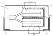
図3に実施例4におけるニオブ固体電解コンデンサの縦断面図を示す。CV積96000μFV/gのニオブ粉末29.5mgを陽極リード部材(1a)として用いる直径0.3mmの植立ニオブワイヤと共に厚さ0.85mmの直方体に焼結し陽極体(1)を作製した。これをリン酸水溶液中において45Vで化成し陽極体(1)表面に誘電体皮膜(2)を形成し、その後ポリピロールを素子内部及び外周に重合析出させ陰極層(3)を形成してコンデンサ素子(10)を作製した。次いで、コンデンサ素子(10)の表面にカーボン懸濁水でカーボン層(4)を形成し、該カーボン層(4)を形成した2つのコンデンサ素子(10)(10)を、銀粉と樹脂を練ったものからなる銀ペースト浴に浸漬し、該2つのコンデンサ素子(10)(10)にて陰極端子(21)を挟み込み乾燥させて、陰極端子(21)を2つのコンデンサ素子(10)(10)に電気的に接続すると共に、2つのコンデンサ素子(10)(10)が一面を共有する金属ペースト層(5)を形成する。その後、射出成形により外装樹脂(7)を形成し、陽極端子(20)及び陰極端子(21)をそれぞれ前記外装樹脂(7)に沿って折り曲げ外形7.3(長さ)×4.3(幅)×2.8(厚さ)mmのニオブ固体電解コンデンサを作製した。
(比較例1−1)
実施例1と同様の方法にてコンデンサ本体を作成し、該コンデンサ本体を折り曲げ加工が施された陰極端子上に載置し導電性接着剤により電気的に接続して固定する。次いで、前記コンデンサ本体から導出している陽極リード部材を陽極端子に抵抗溶接により所定位置に溶接接続する。その後、射出成形により外装樹脂を形成し、陽極端子及び陰極端子をそれぞれ前記外装樹脂に沿って折り曲げ外形7.3(長さ)×4.3(幅)×1.8(厚さ)mmのニオブ固体電解コンデンサを作製した。
(比較例1−2)
実施例1と同様の方法にてコンデンサ本体を作成し、該二つのコンデンサ本体夫々の銀層を銀ペーストからなる導電性接着剤により接続し、該接続された二つのコンデンサ本体を折り曲げ加工が施された陰極端子上に載置し導電性接着剤により電気的に接続して固定する。次いで、前記コンデンサ本体から導出している夫々の陽極リード部材を陽極端子に抵抗溶接により所定位置に溶接接続する。その後、射出成形により外装樹脂を形成し、陽極端子及び陰極端子をそれぞれ前記外装樹脂に沿って折り曲げ外形7.3(長さ)×4.3(幅)×2.8(厚さ)mmのニオブ固体電解コンデンサを作製した。
(比較例1−3)
CV積96000μFV/gのニオブ粉末59mgを直径0.3mmの植立ニオブワイヤと共に厚さ1.7mmの直方体に焼結した以外は実施例1と同様の方法でコンデンサ本体を作成した。その後、該コンデンサ本体を折り曲げ加工が施された陰極端子上に載置し導電性接着剤により電気的に接続して固定する。次いで、前記コンデンサ本体から導出している陽極リード部材を陽極端子に抵抗溶接により所定位置に溶接接続する。その後、射出成形により外装樹脂を形成し、陽極端子及び陰極端子をそれぞれ前記外装樹脂に沿って折り曲げ外形7.3(長さ)×4.3(幅)×2.8(厚さ)mmのニオブ固体電解コンデンサを作製した。
(比較例2−1)
実施例2と同様の方法を用いてコンデンサ本体を作成し、該コンデンサ本体を用いて比較例1−1と同様の方法を用いて7.3(長さ)×4.3(幅)×2.8(厚さ)mmのニオブ固体電解コンデンサを作製した。
(比較例2−2)
実施例2と同様の方法を用いてコンデンサ本体を作成し、該コンデンサ本体を二つ用いて比較例1−2と同様の方法を用いて7.3(長さ)×4.3(幅)×3.8(厚さ)mmのニオブ固体電解コンデンサを作製した。
(比較例3−1)
実施例3と同様の方法を用いてコンデンサ本体を作成し、該コンデンサ本体を用いて比較例1−1と同様の方法を用いて10.0(長さ)×6.3(幅)×1.8(厚さ)mmのニオブ固体電解コンデンサを作製した。
Thereafter, the cathode terminal (21) is sandwiched between the two capacitor bodies (15) through the conductive adhesive (8) made of silver paste, and each metal paste layer (5) and the cathode terminal (21) are sandwiched. Are electrically connected and fixed. Next, each anode lead member (1a) led out from the capacitor main body (15) is welded to a predetermined position by resistance welding to the anode terminal. Thereafter, the exterior resin (7) is formed by injection molding, and the anode terminal (20) and the cathode terminal (21) are bent along the exterior resin (20), respectively, and the outer shape is 7.3 (length) × 4.3 ( A niobium solid electrolytic capacitor having a width (width) × 2.8 (thickness) mm was produced.
(Example 2)
Except that 47 mg of niobium powder having a CV product of 96000 μFV / g was sintered into a rectangular parallelepiped having a thickness of 1.3 mm, the outer shape 7.3 (length) × 4.3 (width) × was used in the same manner as in Example 1. A 3.8 (thickness) niobium solid electrolytic capacitor was produced.
(Example 3)
External form 10.0 (length) x 6.3 (width) x using the same method as in Example 1 except that 92 mg of niobium powder having a CV product of 96000 μFV / g was sintered into a rectangular parallelepiped with a thickness of 0.85 mm. A 2.8 (thickness) niobium solid electrolytic capacitor was produced.
Example 4
FIG. 3 shows a longitudinal sectional view of the niobium solid electrolytic capacitor in Example 4. An anode body (1) was prepared by sintering 29.5 mg of niobium powder having a CV product of 96000 μFV / g together with an implanted niobium wire having a diameter of 0.3 mm as an anode lead member (1a) into a rectangular parallelepiped having a thickness of 0.85 mm. This is formed in a phosphoric acid aqueous solution at 45 V to form a dielectric film (2) on the surface of the anode body (1), and then polypyrrole is polymerized and deposited inside and around the element to form a cathode layer (3) to form a capacitor element. (10) was produced. Next, a carbon layer (4) is formed with carbon suspension water on the surface of the capacitor element (10), and the two capacitor elements (10) and (10) having the carbon layer (4) are kneaded with silver powder and a resin. Immerse it in a silver paste bath made of material, sandwich the cathode terminal (21) between the two capacitor elements (10) and (10), and dry the cathode terminal (21) to the two capacitor elements (10) and (10). And a metal paste layer (5) in which the two capacitor elements (10) and (10) share one surface. Thereafter, the exterior resin (7) is formed by injection molding, and the anode terminal (20) and the cathode terminal (21) are bent along the exterior resin (7), respectively, and the outer shape is 7.3 (length) × 4.3 ( A niobium solid electrolytic capacitor having a width (width) × 2.8 (thickness) mm was produced.
(Comparative Example 1-1)
A capacitor body is prepared in the same manner as in Example 1, and the capacitor body is placed on the bent cathode terminal and electrically connected and fixed by a conductive adhesive. Next, the anode lead member led out from the capacitor body is welded to a predetermined position by resistance welding to the anode terminal. Thereafter, an exterior resin is formed by injection molding, and the anode terminal and the cathode terminal are bent along the exterior resin, respectively, so that the outer shape is 7.3 (length) × 4.3 (width) × 1.8 (thickness) mm. A niobium solid electrolytic capacitor was produced.
(Comparative Example 1-2)
A capacitor body is prepared in the same manner as in Example 1, the silver layers of the two capacitor bodies are connected with a conductive adhesive made of silver paste, and the two connected capacitor bodies are bent. It is placed on the cathode terminal and electrically connected and fixed by a conductive adhesive. Next, each anode lead member led out from the capacitor main body is welded to a predetermined position by resistance welding to the anode terminal. Thereafter, an exterior resin is formed by injection molding, and the anode terminal and the cathode terminal are bent along the exterior resin, respectively, so that the outer shape is 7.3 (length) × 4.3 (width) × 2.8 (thickness) mm. A niobium solid electrolytic capacitor was produced.
(Comparative Example 1-3)
A capacitor main body was prepared in the same manner as in Example 1 except that 59 mg of niobium powder having a CV product of 96000 μFV / g was sintered together with a planted niobium wire having a diameter of 0.3 mm into a rectangular solid having a thickness of 1.7 mm. Thereafter, the capacitor body is placed on the cathode terminal that has been subjected to the bending process, and is electrically connected and fixed by a conductive adhesive. Next, the anode lead member led out from the capacitor body is welded to a predetermined position by resistance welding to the anode terminal. Thereafter, an exterior resin is formed by injection molding, and the anode terminal and the cathode terminal are bent along the exterior resin, respectively, so that the outer shape is 7.3 (length) × 4.3 (width) × 2.8 (thickness) mm. A niobium solid electrolytic capacitor was produced.
(Comparative Example 2-1)
A capacitor body was prepared using the same method as in Example 2, and 7.3 (length) × 4.3 (width) × 2 using the same method as in Comparative Example 1-1 using the capacitor body. A niobium solid electrolytic capacitor of .8 (thickness) mm was produced.
(Comparative Example 2-2)
A capacitor body was prepared using the same method as in Example 2, and 7.3 (length) x 4.3 (width) using the two capacitor bodies and the same method as in Comparative Example 1-2. A niobium solid electrolytic capacitor of × 3.8 (thickness) mm was produced.
(Comparative Example 3-1)
A capacitor body was prepared using the same method as in Example 3, and 10.0 (length) × 6.3 (width) × 1 using the same method as in Comparative Example 1-1 using the capacitor body. A niobium solid electrolytic capacitor of .8 (thickness) mm was produced.
以上の実施例及び比較例のニオブ固体電解コンデンサを作成後、夫々エージング処理を行い、その後静電容量及び100kHzでのESRを夫々測定した。その結果を表1に示す。 After producing the niobium solid electrolytic capacitors of the above examples and comparative examples, aging treatment was performed, respectively, and then the capacitance and ESR at 100 kHz were measured. The results are shown in Table 1.

実施例1のサイズはEIAJ-RC2378-101(表面実装用タンタル固体(導電性高分子)コンデンサ)に規定する寸法記号「7343」に相当する。参考までに同規格の100μV/10VにおけるESR規格は45mΩ以下となっている。実施例1のESR値19mΩは、実施例1のコンデンサ本体1つで作製された比較例1−1の36.8mΩの2個の並列になるため、計算値の18.4mΩに対し達成率97%である。これに対し2つのコンデンサ本体夫々の金属ペースト層を導電性接着剤により接続した従来品の比較例1−2では、25.2mΩなので達成率は73%に過ぎない。この結果より本発明を用いることにより従来品よりESRを25%低減できた。また、実施例1〜3のように1つのコンデンサ本体から作製した従来品のESR値は、32.7mΩと大きい。 The size of Example 1 corresponds to the dimension symbol “7343” defined in EIAJ-RC2378-101 (tantalum solid (conductive polymer) capacitor for surface mounting). For reference, the ESR standard at 100 μV / 10 V of the standard is 45 mΩ or less. The ESR value of 19 mΩ in Example 1 is parallel to the 36.8 mΩ of Comparative Example 1-1 produced by one capacitor body of Example 1, so that the achievement rate is 97 against the calculated value of 18.4 mΩ. %. On the other hand, in the comparative example 1-2 of the conventional product in which the metal paste layers of the two capacitor bodies are connected by the conductive adhesive, the achievement rate is only 73% because it is 25.2 mΩ. From this result, ESR was reduced by 25% compared to the conventional product by using the present invention. Moreover, the ESR value of the conventional product manufactured from one capacitor body as in Examples 1 to 3 is as large as 32.7 mΩ.
実施例2は、実施例1と長さと幅は同寸法にして厚く形成したものである。この場合も実施例2のコンデンサ本体1つで作製された比較例2−1の32.7mΩの2個の並列になるため、計算値16.4mΩの達成率95%である。これに対し二つのコンデンサ本体夫々の金属ペースト層を導電性接着剤により接続した従来技術の75%に過ぎない。 In Example 2, the length and width are the same as those in Example 1, and the thickness is increased. Also in this case, since the 32.7 mΩ in parallel of Comparative Example 2-1 manufactured with one capacitor body of Example 2 is paralleled, the achievement rate of calculated value 16.4 mΩ is 95%. On the other hand, only 75% of the prior art in which the metal paste layers of the two capacitor bodies are connected by a conductive adhesive.
また、実施例3は長さと幅を大きくとり厚さを薄くしたものだが、この場合ESRの絶対値は小さくなるが達成率は、比較例3−1から計算して96%とやはり高い。 In Example 3, the length and width are increased and the thickness is reduced. In this case, the absolute value of ESR is reduced, but the achievement rate is still high as 96% calculated from Comparative Example 3-1.
ニオブ焼結体を用いた本発明の実施例1〜3において計算値の95〜97%と従来品の約73%に対し非常に高い達成率が得られた。この結果、従来の2つのコンデンサ本体夫々の金属ペースト層を導電性接着剤により接続した従来品に比べESRを23〜25%低減することができた。 In Examples 1 to 3 of the present invention using a niobium sintered body, a very high achievement rate was obtained for 95 to 97% of the calculated value and about 73% of the conventional product. As a result, ESR was reduced by 23 to 25% compared to the conventional product in which the metal paste layers of the two conventional capacitor bodies were connected by the conductive adhesive.
これは、誘電体皮膜から陰極引出層までの平均パスの距離を短くする素子2分割化によるESR低減効果が、陽極体としてニオブ用いた場合、タンタル等の他の弁金属を用いた場合よりも著しく大きいことと、該素子2分割化により2つのコンデンサ本体を導電性接着剤等により接続するための、金属ペースト層における表皮の樹脂だけの薄膜同士を接続することによる高抵抗部が形成されないこととの相乗効果を得られるためと考えられる。 This is because the ESR reduction effect by dividing the element into two elements that shorten the average path distance from the dielectric film to the cathode lead layer is more effective when niobium is used as the anode body than when other valve metal such as tantalum is used. It is extremely large, and the high resistance part is not formed by connecting the thin film of the skin resin only in the metal paste layer for connecting the two capacitor bodies with the conductive adhesive by dividing the element into two parts. This is thought to be because of a synergistic effect.
実施例4は、カーボン層(4)が形成された2つのコンデンサ素子(10)(10)の一面を共有する金属ペースト層(5)を形成し、前記共有している金属ペースト層(5)内に陰極端子(21)が配置した構成になっている。この構造を用いることにより、金属ペースト層(5)における表皮の表面に形成されやすい樹脂だけの薄膜がなくなると共に、導電性接着剤も使用したいため実施例1〜3よりもESR低減効果がさらに大きくなる。 In Example 4, the metal paste layer (5) sharing one surface of the two capacitor elements (10) and (10) formed with the carbon layer (4) is formed, and the shared metal paste layer (5) is formed. The cathode terminal (21) is arranged inside. By using this structure, there is no thin resin-only thin film that is easily formed on the surface of the skin in the metal paste layer (5), and a conductive adhesive is also used, so the ESR reduction effect is even greater than in Examples 1-3. Become.
実施例では、陽極リード部材として植立ニオブワイヤを用いたが代わりにタンタルワイヤを用いてもよく、またニオブ粉末焼結後にニオブワイヤを溶接接続してもよい。また、ワイヤの代わりに板材を用いることもできる。また、金属ペースト層に用いる金属粉の形状として燐片状のものを用いたが、フレーク状のものを用いても同様の効果を得ることができる。 In the embodiment, the planted niobium wire is used as the anode lead member, but a tantalum wire may be used instead, and the niobium wire may be welded after the niobium powder is sintered. A plate material can also be used instead of the wire. Moreover, although the flake shaped thing was used as the shape of the metal powder used for a metal paste layer, the same effect can be acquired even if it uses a flake shaped thing.
また、金属ペースト層内における説明で樹脂だけの薄膜とは、完全に樹脂のみを示すものではなく、金属粉に対して樹脂が多いものも含む。 In the description in the metal paste layer, the resin-only thin film does not completely indicate the resin, but includes a resin that contains more resin than the metal powder.
1 陽極体
1a 陽極リード部材
2 誘電体皮膜
3 陰極層
4 カーボン層
5 金属ペースト層
5a 金属粉
5b 樹脂
7 外装樹脂
8 導電性接着剤
10 コンデンサ素子
15 コンデンサ本体
21 陽極端子
22 陰極端子
1 Anode body
1a
5a metal powder
Claims (2)
コンデンサ本体(15)の夫々の陽極リード部材(1a)に電気的に接続された陽極端子(20)と、
2つのコンデンサ本体(15)(15)に挟まれて電気的に接続された陰極端子(21)と、
2つのコンデンサ本体(15)(15)、陽極端子(20)及び陰極端子(21)を被覆して、これらを一体モールドしてなる外装樹脂(7)とからなり、前記陽極端子(20)及び陰極端子(21)は夫々の一部が前記外装樹脂(7)から露出していることを特徴とするニオブ固体電解コンデンサ。 An anode body (1) made of a powder sintered body mainly composed of niobium or a niobium compound is provided with an anode lead member (1a), and a dielectric film (2) and a cathode layer (on the surface of the anode body (1)). 3) A capacitor element (10) formed with a carbon layer (4) and a metal paste layer (5) to form a capacitor body (15), and niobium having two capacitor bodies (15) In solid electrolytic capacitors,
An anode terminal (20) electrically connected to each anode lead member (1a) of the capacitor body (15);
A cathode terminal (21) electrically connected between two capacitor bodies (15) (15);
Two capacitor bodies (15), (15), an anode terminal (20), and a cathode terminal (21) are coated with an exterior resin (7) formed by integrally molding them, and the anode terminal (20) and A niobium solid electrolytic capacitor, wherein each of the cathode terminals (21) is exposed from the exterior resin (7).
前記コンデンサ素子(10)の夫々の陽極リード部材(1a)に電気的に接続された陽極端子(20)と、
カーボン層まで形成した2つのコンデンサ素子(10)(10)の表面に形成され、且つ、前記2つのコンデンサ素子(10)(10)の一面を共有している金属ペースト層(5)と、
前記共有している金属ペースト層(5)内に配置された陰極端子(21)と、
2つのコンデンサ素子(10)(10)、陽極端子(20)及び陰極端子(21)を被覆して、これらを一体モールドしてなる外装樹脂(7)とからなり、前記陽極端子(20)及び陰極端子(21)は夫々の一部が前記外装樹脂(7)から露出していることを特徴とするニオブ固体電解コンデンサ。
An anode body (1) made of a powder sintered body mainly composed of niobium or a niobium compound is provided with an anode lead member (1a), and a dielectric film (2) and a cathode layer (on the surface of the anode body (1)). In a niobium solid electrolytic capacitor comprising a capacitor element (10) formed with 3), a carbon layer (4), and two capacitor elements (10) formed up to the carbon layer.
An anode terminal (20) electrically connected to each anode lead member (1a) of the capacitor element (10);
A metal paste layer (5) formed on the surfaces of the two capacitor elements (10) (10) formed up to the carbon layer and sharing one surface of the two capacitor elements (10) (10);
A cathode terminal (21) disposed in the shared metal paste layer (5);
Two capacitor elements (10), (10), an anode terminal (20), and a cathode terminal (21) are coated with an exterior resin (7) formed by integrally molding them, and the anode terminal (20) and A niobium solid electrolytic capacitor, wherein each of the cathode terminals (21) is exposed from the exterior resin (7).
Priority Applications (1)
| Application Number | Priority Date | Filing Date | Title |
|---|---|---|---|
| JP2004125135A JP2005311014A (en) | 2004-04-21 | 2004-04-21 | Niobium solid electrolytic capacitor |
Applications Claiming Priority (1)
| Application Number | Priority Date | Filing Date | Title |
|---|---|---|---|
| JP2004125135A JP2005311014A (en) | 2004-04-21 | 2004-04-21 | Niobium solid electrolytic capacitor |
Publications (1)
| Publication Number | Publication Date |
|---|---|
| JP2005311014A true JP2005311014A (en) | 2005-11-04 |
Family
ID=35439437
Family Applications (1)
| Application Number | Title | Priority Date | Filing Date |
|---|---|---|---|
| JP2004125135A Pending JP2005311014A (en) | 2004-04-21 | 2004-04-21 | Niobium solid electrolytic capacitor |
Country Status (1)
| Country | Link |
|---|---|
| JP (1) | JP2005311014A (en) |
Cited By (2)
| Publication number | Priority date | Publication date | Assignee | Title |
|---|---|---|---|---|
| JP2007300123A (en) * | 2006-04-28 | 2007-11-15 | Avx Corp | Solid electrolytic capacitor assembly |
| WO2014116843A1 (en) * | 2013-01-25 | 2014-07-31 | Kemet Electronics Corporation | Solid electrolytic capacitor and method of manufacture |
-
2004
- 2004-04-21 JP JP2004125135A patent/JP2005311014A/en active Pending
Cited By (3)
| Publication number | Priority date | Publication date | Assignee | Title |
|---|---|---|---|---|
| JP2007300123A (en) * | 2006-04-28 | 2007-11-15 | Avx Corp | Solid electrolytic capacitor assembly |
| WO2014116843A1 (en) * | 2013-01-25 | 2014-07-31 | Kemet Electronics Corporation | Solid electrolytic capacitor and method of manufacture |
| US9941056B2 (en) | 2013-01-25 | 2018-04-10 | Kemet Electronics Corporation | Solid electrolytic capacitor and method |
Similar Documents
| Publication | Publication Date | Title |
|---|---|---|
| TWI478189B (en) | Solid electrolytic capacitor and method of manufacturing thereof | |
| JP2010153454A (en) | Solid electrolytic capacitor | |
| US20150155101A1 (en) | Forming Method of Solid Electrolytic Capacitor | |
| CN1774778B (en) | Sintered body electrode and solid electrolytic capacitor using the electrode | |
| JP5020020B2 (en) | Manufacturing method of solid electrolytic capacitor | |
| JP5623214B2 (en) | Solid electrolytic capacitor | |
| JPWO2013088845A1 (en) | Solid electrolytic capacitor | |
| JP3454715B2 (en) | Method for manufacturing solid electrolytic capacitor | |
| EP3767654A1 (en) | Solid electrolytic capacitor and method for manufacturing solid electrolytic capacitor | |
| KR20210061616A (en) | Solid Electrolyte Capacitor and fabrication method thereof | |
| JP2011216649A (en) | Method of manufacturing solid-state electrolytic capacitor | |
| JP2017022222A (en) | Solid electrolytic capacitor and manufacturing method of the same | |
| CN1930647B (en) | Solid electrolytic capacitor and the use thereof | |
| US8882857B2 (en) | Solid electrolytic capacitor and method for manufacturing the same | |
| US20160181021A1 (en) | Solid electrolyte capacitor and manufacturing method thereof | |
| JP5611745B2 (en) | Solid electrolytic capacitor manufacturing method and solid electrolytic capacitor | |
| JP2005311014A (en) | Niobium solid electrolytic capacitor | |
| JP4624017B2 (en) | Manufacturing method of solid electrolytic capacitor | |
| JP2019067923A (en) | Solid electrolytic capacitor and method for manufacturing the same | |
| WO2017163724A1 (en) | Solid electrolytic capacitor | |
| JP2006278788A (en) | Solid electrolytic capacitor and its manufacturing method | |
| KR102016481B1 (en) | Solid Electrolyte Capacitor and fabrication method thereof | |
| JP3546451B2 (en) | Method for manufacturing solid electrolytic capacitor | |
| US10181382B2 (en) | Solid electrolytic capacitor | |
| JP3454733B2 (en) | Method for manufacturing solid electrolytic capacitor |
Legal Events
| Date | Code | Title | Description |
|---|---|---|---|
| RD01 | Notification of change of attorney |
Effective date: 20051227 Free format text: JAPANESE INTERMEDIATE CODE: A7421 |
|
| A621 | Written request for application examination |
Effective date: 20061115 Free format text: JAPANESE INTERMEDIATE CODE: A621 |
|
| A977 | Report on retrieval |
Free format text: JAPANESE INTERMEDIATE CODE: A971007 Effective date: 20080829 |
|
| A131 | Notification of reasons for refusal |
Free format text: JAPANESE INTERMEDIATE CODE: A131 Effective date: 20080909 |
|
| A521 | Written amendment |
Effective date: 20081106 Free format text: JAPANESE INTERMEDIATE CODE: A523 |
|
| A02 | Decision of refusal |
Free format text: JAPANESE INTERMEDIATE CODE: A02 Effective date: 20090428 |