JP2005268497A - Semiconductor device and manufacturing method of semiconductor device - Google Patents
Semiconductor device and manufacturing method of semiconductor device Download PDFInfo
- Publication number
- JP2005268497A JP2005268497A JP2004078244A JP2004078244A JP2005268497A JP 2005268497 A JP2005268497 A JP 2005268497A JP 2004078244 A JP2004078244 A JP 2004078244A JP 2004078244 A JP2004078244 A JP 2004078244A JP 2005268497 A JP2005268497 A JP 2005268497A
- Authority
- JP
- Japan
- Prior art keywords
- balls
- semiconductor chip
- stacked
- ball
- bonding
- Prior art date
- Legal status (The legal status is an assumption and is not a legal conclusion. Google has not performed a legal analysis and makes no representation as to the accuracy of the status listed.)
- Pending
Links
Images


Classifications
-
- B—PERFORMING OPERATIONS; TRANSPORTING
- B23—MACHINE TOOLS; METAL-WORKING NOT OTHERWISE PROVIDED FOR
- B23K—SOLDERING OR UNSOLDERING; WELDING; CLADDING OR PLATING BY SOLDERING OR WELDING; CUTTING BY APPLYING HEAT LOCALLY, e.g. FLAME CUTTING; WORKING BY LASER BEAM
- B23K20/00—Non-electric welding by applying impact or other pressure, with or without the application of heat, e.g. cladding or plating
- B23K20/002—Non-electric welding by applying impact or other pressure, with or without the application of heat, e.g. cladding or plating specially adapted for particular articles or work
- B23K20/004—Wire welding
- B23K20/005—Capillary welding
- B23K20/007—Ball bonding
-
- H—ELECTRICITY
- H10—SEMICONDUCTOR DEVICES; ELECTRIC SOLID-STATE DEVICES NOT OTHERWISE PROVIDED FOR
- H10W—GENERIC PACKAGES, INTERCONNECTIONS, CONNECTORS OR OTHER CONSTRUCTIONAL DETAILS OF DEVICES COVERED BY CLASS H10
- H10W90/00—Package configurations
- H10W90/811—Multiple chips on leadframes
-
- H—ELECTRICITY
- H10—SEMICONDUCTOR DEVICES; ELECTRIC SOLID-STATE DEVICES NOT OTHERWISE PROVIDED FOR
- H10W—GENERIC PACKAGES, INTERCONNECTIONS, CONNECTORS OR OTHER CONSTRUCTIONAL DETAILS OF DEVICES COVERED BY CLASS H10
- H10W72/00—Interconnections or connectors in packages
- H10W72/01—Manufacture or treatment
- H10W72/015—Manufacture or treatment of bond wires
- H10W72/01551—Changing the shapes of bond wires
-
- H—ELECTRICITY
- H10—SEMICONDUCTOR DEVICES; ELECTRIC SOLID-STATE DEVICES NOT OTHERWISE PROVIDED FOR
- H10W—GENERIC PACKAGES, INTERCONNECTIONS, CONNECTORS OR OTHER CONSTRUCTIONAL DETAILS OF DEVICES COVERED BY CLASS H10
- H10W72/00—Interconnections or connectors in packages
- H10W72/071—Connecting or disconnecting
- H10W72/0711—Apparatus therefor
- H10W72/07141—Means for applying energy, e.g. ovens or lasers
-
- H—ELECTRICITY
- H10—SEMICONDUCTOR DEVICES; ELECTRIC SOLID-STATE DEVICES NOT OTHERWISE PROVIDED FOR
- H10W—GENERIC PACKAGES, INTERCONNECTIONS, CONNECTORS OR OTHER CONSTRUCTIONAL DETAILS OF DEVICES COVERED BY CLASS H10
- H10W72/00—Interconnections or connectors in packages
- H10W72/071—Connecting or disconnecting
- H10W72/075—Connecting or disconnecting of bond wires
- H10W72/07511—Treating the bonding area before connecting, e.g. by applying flux or cleaning
-
- H—ELECTRICITY
- H10—SEMICONDUCTOR DEVICES; ELECTRIC SOLID-STATE DEVICES NOT OTHERWISE PROVIDED FOR
- H10W—GENERIC PACKAGES, INTERCONNECTIONS, CONNECTORS OR OTHER CONSTRUCTIONAL DETAILS OF DEVICES COVERED BY CLASS H10
- H10W72/00—Interconnections or connectors in packages
- H10W72/071—Connecting or disconnecting
- H10W72/075—Connecting or disconnecting of bond wires
- H10W72/07521—Aligning
-
- H—ELECTRICITY
- H10—SEMICONDUCTOR DEVICES; ELECTRIC SOLID-STATE DEVICES NOT OTHERWISE PROVIDED FOR
- H10W—GENERIC PACKAGES, INTERCONNECTIONS, CONNECTORS OR OTHER CONSTRUCTIONAL DETAILS OF DEVICES COVERED BY CLASS H10
- H10W72/00—Interconnections or connectors in packages
- H10W72/071—Connecting or disconnecting
- H10W72/075—Connecting or disconnecting of bond wires
- H10W72/07531—Techniques
- H10W72/07532—Compression bonding, e.g. thermocompression bonding
- H10W72/07533—Ultrasonic bonding, e.g. thermosonic bonding
-
- H—ELECTRICITY
- H10—SEMICONDUCTOR DEVICES; ELECTRIC SOLID-STATE DEVICES NOT OTHERWISE PROVIDED FOR
- H10W—GENERIC PACKAGES, INTERCONNECTIONS, CONNECTORS OR OTHER CONSTRUCTIONAL DETAILS OF DEVICES COVERED BY CLASS H10
- H10W72/00—Interconnections or connectors in packages
- H10W72/071—Connecting or disconnecting
- H10W72/075—Connecting or disconnecting of bond wires
- H10W72/07551—Connecting or disconnecting of bond wires characterised by changes in properties of the bond wires during the connecting
- H10W72/07553—Connecting or disconnecting of bond wires characterised by changes in properties of the bond wires during the connecting changes in shapes
-
- H—ELECTRICITY
- H10—SEMICONDUCTOR DEVICES; ELECTRIC SOLID-STATE DEVICES NOT OTHERWISE PROVIDED FOR
- H10W—GENERIC PACKAGES, INTERCONNECTIONS, CONNECTORS OR OTHER CONSTRUCTIONAL DETAILS OF DEVICES COVERED BY CLASS H10
- H10W72/00—Interconnections or connectors in packages
- H10W72/50—Bond wires
- H10W72/531—Shapes of wire connectors
- H10W72/536—Shapes of wire connectors the connected ends being ball-shaped
-
- H—ELECTRICITY
- H10—SEMICONDUCTOR DEVICES; ELECTRIC SOLID-STATE DEVICES NOT OTHERWISE PROVIDED FOR
- H10W—GENERIC PACKAGES, INTERCONNECTIONS, CONNECTORS OR OTHER CONSTRUCTIONAL DETAILS OF DEVICES COVERED BY CLASS H10
- H10W72/00—Interconnections or connectors in packages
- H10W72/50—Bond wires
- H10W72/531—Shapes of wire connectors
- H10W72/5363—Shapes of wire connectors the connected ends being wedge-shaped
-
- H—ELECTRICITY
- H10—SEMICONDUCTOR DEVICES; ELECTRIC SOLID-STATE DEVICES NOT OTHERWISE PROVIDED FOR
- H10W—GENERIC PACKAGES, INTERCONNECTIONS, CONNECTORS OR OTHER CONSTRUCTIONAL DETAILS OF DEVICES COVERED BY CLASS H10
- H10W72/00—Interconnections or connectors in packages
- H10W72/50—Bond wires
- H10W72/531—Shapes of wire connectors
- H10W72/5366—Shapes of wire connectors the bond wires having kinks
-
- H—ELECTRICITY
- H10—SEMICONDUCTOR DEVICES; ELECTRIC SOLID-STATE DEVICES NOT OTHERWISE PROVIDED FOR
- H10W—GENERIC PACKAGES, INTERCONNECTIONS, CONNECTORS OR OTHER CONSTRUCTIONAL DETAILS OF DEVICES COVERED BY CLASS H10
- H10W72/00—Interconnections or connectors in packages
- H10W72/50—Bond wires
- H10W72/541—Dispositions of bond wires
- H10W72/5434—Dispositions of bond wires the connected ends being on auxiliary connecting means on bond pads, e.g. on other bond wires
-
- H—ELECTRICITY
- H10—SEMICONDUCTOR DEVICES; ELECTRIC SOLID-STATE DEVICES NOT OTHERWISE PROVIDED FOR
- H10W—GENERIC PACKAGES, INTERCONNECTIONS, CONNECTORS OR OTHER CONSTRUCTIONAL DETAILS OF DEVICES COVERED BY CLASS H10
- H10W72/00—Interconnections or connectors in packages
- H10W72/50—Bond wires
- H10W72/541—Dispositions of bond wires
- H10W72/547—Dispositions of multiple bond wires
- H10W72/5473—Dispositions of multiple bond wires multiple bond wires connected to a common bond pad
-
- H—ELECTRICITY
- H10—SEMICONDUCTOR DEVICES; ELECTRIC SOLID-STATE DEVICES NOT OTHERWISE PROVIDED FOR
- H10W—GENERIC PACKAGES, INTERCONNECTIONS, CONNECTORS OR OTHER CONSTRUCTIONAL DETAILS OF DEVICES COVERED BY CLASS H10
- H10W72/00—Interconnections or connectors in packages
- H10W72/50—Bond wires
- H10W72/551—Materials of bond wires
- H10W72/552—Materials of bond wires comprising metals or metalloids, e.g. silver
- H10W72/5522—Materials of bond wires comprising metals or metalloids, e.g. silver comprising gold [Au]
-
- H—ELECTRICITY
- H10—SEMICONDUCTOR DEVICES; ELECTRIC SOLID-STATE DEVICES NOT OTHERWISE PROVIDED FOR
- H10W—GENERIC PACKAGES, INTERCONNECTIONS, CONNECTORS OR OTHER CONSTRUCTIONAL DETAILS OF DEVICES COVERED BY CLASS H10
- H10W72/00—Interconnections or connectors in packages
- H10W72/50—Bond wires
- H10W72/581—Auxiliary members, e.g. flow barriers
- H10W72/583—Reinforcing structures
-
- H—ELECTRICITY
- H10—SEMICONDUCTOR DEVICES; ELECTRIC SOLID-STATE DEVICES NOT OTHERWISE PROVIDED FOR
- H10W—GENERIC PACKAGES, INTERCONNECTIONS, CONNECTORS OR OTHER CONSTRUCTIONAL DETAILS OF DEVICES COVERED BY CLASS H10
- H10W72/00—Interconnections or connectors in packages
- H10W72/50—Bond wires
- H10W72/59—Bond pads specially adapted therefor
-
- H—ELECTRICITY
- H10—SEMICONDUCTOR DEVICES; ELECTRIC SOLID-STATE DEVICES NOT OTHERWISE PROVIDED FOR
- H10W—GENERIC PACKAGES, INTERCONNECTIONS, CONNECTORS OR OTHER CONSTRUCTIONAL DETAILS OF DEVICES COVERED BY CLASS H10
- H10W72/00—Interconnections or connectors in packages
- H10W72/90—Bond pads, in general
- H10W72/931—Shapes of bond pads
- H10W72/934—Cross-sectional shape, i.e. in side view
-
- H—ELECTRICITY
- H10—SEMICONDUCTOR DEVICES; ELECTRIC SOLID-STATE DEVICES NOT OTHERWISE PROVIDED FOR
- H10W—GENERIC PACKAGES, INTERCONNECTIONS, CONNECTORS OR OTHER CONSTRUCTIONAL DETAILS OF DEVICES COVERED BY CLASS H10
- H10W72/00—Interconnections or connectors in packages
- H10W72/90—Bond pads, in general
- H10W72/951—Materials of bond pads
-
- H—ELECTRICITY
- H10—SEMICONDUCTOR DEVICES; ELECTRIC SOLID-STATE DEVICES NOT OTHERWISE PROVIDED FOR
- H10W—GENERIC PACKAGES, INTERCONNECTIONS, CONNECTORS OR OTHER CONSTRUCTIONAL DETAILS OF DEVICES COVERED BY CLASS H10
- H10W90/00—Package configurations
- H10W90/20—Configurations of stacked chips
- H10W90/24—Configurations of stacked chips at least one of the stacked chips being laterally offset from a neighbouring stacked chip, e.g. chip stacks having a staircase shape
-
- H—ELECTRICITY
- H10—SEMICONDUCTOR DEVICES; ELECTRIC SOLID-STATE DEVICES NOT OTHERWISE PROVIDED FOR
- H10W—GENERIC PACKAGES, INTERCONNECTIONS, CONNECTORS OR OTHER CONSTRUCTIONAL DETAILS OF DEVICES COVERED BY CLASS H10
- H10W90/00—Package configurations
- H10W90/701—Package configurations characterised by the relative positions of pads or connectors relative to package parts
- H10W90/731—Package configurations characterised by the relative positions of pads or connectors relative to package parts of die-attach connectors
- H10W90/732—Package configurations characterised by the relative positions of pads or connectors relative to package parts of die-attach connectors between stacked chips
-
- H—ELECTRICITY
- H10—SEMICONDUCTOR DEVICES; ELECTRIC SOLID-STATE DEVICES NOT OTHERWISE PROVIDED FOR
- H10W—GENERIC PACKAGES, INTERCONNECTIONS, CONNECTORS OR OTHER CONSTRUCTIONAL DETAILS OF DEVICES COVERED BY CLASS H10
- H10W90/00—Package configurations
- H10W90/701—Package configurations characterised by the relative positions of pads or connectors relative to package parts
- H10W90/751—Package configurations characterised by the relative positions of pads or connectors relative to package parts of bond wires
- H10W90/752—Package configurations characterised by the relative positions of pads or connectors relative to package parts of bond wires between stacked chips
-
- H—ELECTRICITY
- H10—SEMICONDUCTOR DEVICES; ELECTRIC SOLID-STATE DEVICES NOT OTHERWISE PROVIDED FOR
- H10W—GENERIC PACKAGES, INTERCONNECTIONS, CONNECTORS OR OTHER CONSTRUCTIONAL DETAILS OF DEVICES COVERED BY CLASS H10
- H10W90/00—Package configurations
- H10W90/701—Package configurations characterised by the relative positions of pads or connectors relative to package parts
- H10W90/751—Package configurations characterised by the relative positions of pads or connectors relative to package parts of bond wires
- H10W90/756—Package configurations characterised by the relative positions of pads or connectors relative to package parts of bond wires between a chip and a stacked lead frame, conducting package substrate or heat sink
Landscapes
- Engineering & Computer Science (AREA)
- Mechanical Engineering (AREA)
- Wire Bonding (AREA)
Abstract
【課題】 半導体チップ上に設ける電極の個数を少なくすると共に、チップサイズを小さくする。
【解決手段】 本発明の半導体装置の製造方法は、半導体チップ3上の電極5上にバンプ形状に加工したAuボール8を積み上げる工程を備え、前記積み上げたAuボール8上にリード電極4上のボールボンドを完了したAu線6をステッチボンドして接続する工程を備え、更に、前記ステッチボンドしたAuボール8上にバンプ形状に加工したAuボール8を積み上げる工程を備えたところに特徴を有する。この製造方法によれば、半導体チップ3上に設ける電極5の個数を少なくすることができ、チップサイズを小さくし得る。
【選択図】 図1
PROBLEM TO BE SOLVED: To reduce the number of electrodes provided on a semiconductor chip and reduce the chip size.
A method for manufacturing a semiconductor device according to the present invention includes a step of stacking Au balls 8 processed into a bump shape on an electrode 5 on a semiconductor chip 3, and a lead electrode 4 is formed on the stacked Au ball 8. The present invention is characterized in that it includes a step of stitch bonding the Au wires 6 that have completed the ball bonding, and a step of stacking the Au balls 8 processed into a bump shape on the stitch bonded Au balls 8. According to this manufacturing method, the number of electrodes 5 provided on the semiconductor chip 3 can be reduced, and the chip size can be reduced.
[Selection] Figure 1
Description
本発明は、半導体チップの電極とリード電極とをワイヤボンディングすることにより接続する構成を備えた半導体装置及び半導体装置の製造方法に関する。 The present invention relates to a semiconductor device having a configuration in which an electrode of a semiconductor chip and a lead electrode are connected by wire bonding and a method for manufacturing the semiconductor device.
半導体装置である例えばLD−MOS等のパワー素子においては、大電流制御のために、半導体チップに複数の電極を設けると共に、複数のAu線を接続可能な大きさのリード電極を設け、半導体チップの複数の電極とリード電極とをそれぞれ1本のAu線でワイヤボンディングするように構成されている。この場合、複数(例えば3個)の電極とリード電極との間は、複数本(例えば3本)のAu線でワイヤボンディングされている。尚、このようなワイヤボンディング技術に関連する技術を示す公報として、特許文献1が知られている。
上記従来構成のパワー素子においては、大電流を流すために、半導体チップ上に多くの電極を設ける必要がある。このため、チップサイズが大きくなり、ひいては、半導体チップを搭載するアイランドのサイズも大きくなってしまうという問題点があった。
そこで、本発明の目的は、半導体チップ上に設ける電極の個数を少なくすることができ、チップサイズを小さくすることができる半導体装置及び半導体装置の製造方法を提供するにある。
In the power device having the above-described conventional configuration, it is necessary to provide a large number of electrodes on the semiconductor chip in order to flow a large current. For this reason, there is a problem that the chip size is increased, and as a result, the size of the island on which the semiconductor chip is mounted is also increased.
Accordingly, an object of the present invention is to provide a semiconductor device and a method for manufacturing the semiconductor device that can reduce the number of electrodes provided on a semiconductor chip and reduce the chip size.
本発明の半導体装置の製造方法は、半導体チップ上の電極上にバンプ形状に加工したAuボールを積み上げる工程と、前記積み上げたAuボール上にリード電極上のボールボンドを完了したAu線をステッチボンドして接続する工程と、前記ステッチボンドしたAuボール上にバンプ形状に加工したAuボールを積み上げる工程とを備えたところに特徴を有するものである。 The method of manufacturing a semiconductor device of the present invention includes a step of stacking Au balls processed into a bump shape on an electrode on a semiconductor chip, and stitch bonding an Au wire having completed ball bonding on a lead electrode on the stacked Au ball. And a step of stacking Au balls processed into bump shapes on the stitch-bonded Au balls.
上記半導体装置の製造方法によれば、半導体チップ上の電極上にAuボールを2個積み上げ、上記1個の電極上にAu線を2本接続することが可能なように構成したので、半導体チップ上に設ける電極の個数を少なくすることができ、チップサイズを小さくすることができる。
また、上記構成の場合、前記2重に積み上げたAuボール上に、リード電極上のボールボンドを完了したAu線をステッチボンドして接続する工程を備えることが好ましい。
According to the semiconductor device manufacturing method, two Au balls are stacked on the electrode on the semiconductor chip, and two Au wires can be connected on the one electrode. The number of electrodes provided on the top can be reduced, and the chip size can be reduced.
Further, in the case of the above configuration, it is preferable to include a step of stitch-bonding and connecting the Au wires that have completed the ball bonding on the lead electrodes on the double stacked Au balls.
更に、前記ステッチボンドしたAuボール上にバンプ形状に加工したAuボールを積み上げる工程と、この積み上げたAuボール上に、リード電極上のボールボンドを完了したAu線をステッチボンドして接続する工程とを、順に複数回繰り返すように構成することがより一層好ましい。 Furthermore, a process of stacking Au balls processed into a bump shape on the stitch-bonded Au balls, and a process of stitch-bonding and connecting Au wires that have completed ball bonding on the lead electrodes on the stacked Au balls; Is more preferably configured to be repeated a plurality of times in order.
一方、本発明の他の半導体装置の製造方法は、リード電極上にバンプ形状に加工したAuボールを積み上げる工程と、前記積み上げたAuボール上に、半導体チップの電極上のボールボンドを完了したAu線をステッチボンドして接続する工程と、前記ステッチボンドしたAuボール上にバンプ形状に加工したAuボールを積み上げる工程とを備えたところに特徴を有する。 Meanwhile, another method of manufacturing a semiconductor device according to the present invention includes a step of stacking Au balls processed into a bump shape on a lead electrode, and an Au that has completed ball bonding on an electrode of a semiconductor chip on the stacked Au balls. It is characterized in that it comprises a step of connecting the wires by stitch bonding, and a step of stacking Au balls processed into a bump shape on the stitch bonded Au balls.
この半導体装置の製造方法によれば、リード電極上にAuボールを2個積み上げ、リード電極上における1箇所の部位にAu線を2本接続することが可能なように構成したので、リード電極のサイズを小さくすることができる。
上記構成の場合、前記2重に積み上げたAuボール上に、半導体チップの電極上のボールボンドを完了したAu線をステッチボンドして接続する工程を備えることが好ましい。
According to this method for manufacturing a semiconductor device, two Au balls are stacked on the lead electrode, and two Au wires can be connected to one part on the lead electrode. The size can be reduced.
In the case of the above configuration, it is preferable to include a step of stitch-bonding and connecting Au wires that have completed ball bonding on the electrodes of the semiconductor chip on the double stacked Au balls.
また、前記ステッチボンドしたAuボール上にバンプ形状に加工したAuボールを積み上げる工程と、この積み上げたAuボール上に、半導体チップの電極上のボールボンドを完了したAu線をステッチボンドして接続する工程とを、順に複数回繰り返すように構成することがより一層良い。 Further, a process of stacking Au balls processed into bump shapes on the stitch-bonded Au balls and stitch-bonding Au wires that have completed ball bonding on the electrodes of the semiconductor chip are connected to the stacked Au balls. It is even better to configure the process so as to be repeated a plurality of times in order.
また、本発明の半導体装置は、半導体チップと、リード電極とを備え、前記半導体チップの電極上にバンプ形状に加工したAuボールを積み上げ、この積み上げたAuボール上にリード電極上のボールボンドを完了したAu線をステッチボンドして接続し、このステッチボンドしたAuボール上にバンプ形状に加工したAuボールを積み上げ、更に、この積み上げたAuボール上に、リード電極上のボールボンドを完了したAu線をステッチボンドして接続するように構成したところに特徴を有するものである。 The semiconductor device of the present invention includes a semiconductor chip and a lead electrode, and Au balls processed into bump shapes are stacked on the electrodes of the semiconductor chip, and a ball bond on the lead electrode is formed on the stacked Au balls. The finished Au wires are connected by stitch bonding, Au balls processed into bump shapes are stacked on the stitch bonded Au balls, and further, the Au balls that have completed the ball bonding on the lead electrodes are stacked on the stacked Au balls. It is characterized in that the wires are connected by stitch bonding.
本発明の他の半導体装置は、半導体チップと、リード電極とを備え、前記リード電極上にバンプ形状に加工したAuボールを積み上げ、この積み上げたAuボール上に、前記半導体チップの1つの電極上のボールボンドを完了したAu線をステッチボンドして接続し、このステッチボンドしたAuボール上にバンプ形状に加工したAuボールを積み上げ、更に、この積み上げたAuボール上に、前記半導体チップの他の電極上のボールボンドを完了したAu線をステッチボンドして接続するように構成したものである。 Another semiconductor device of the present invention includes a semiconductor chip and a lead electrode, and Au balls processed into a bump shape are stacked on the lead electrode, and on the stacked Au ball, one electrode of the semiconductor chip is stacked. The Au wires that have completed the ball bonding are connected by stitch bonding, Au balls processed into bump shapes are stacked on the stitch bonded Au balls, and the other Au chips are further stacked on the stacked Au balls. The Au wire that has completed the ball bond on the electrode is connected by stitch bonding.
また、上記構成の場合、半導体チップを載置するアイランドを備え、このアイランド上に第1の半導体チップを載置すると共に、この第1の半導体チップ上に第2の半導体チップを載置し、前記第1の半導体チップ上における前記第2の半導体チップが載置されていない部分に設けられた電極を前記1つの電極とし、前記第2の半導体チップ上に設けられた電極を前記他の電極とするように構成したところに特徴を有する。 Further, in the case of the above configuration, an island for placing the semiconductor chip is provided, the first semiconductor chip is placed on the island, and the second semiconductor chip is placed on the first semiconductor chip, An electrode provided on a portion of the first semiconductor chip where the second semiconductor chip is not placed is used as the one electrode, and an electrode provided on the second semiconductor chip is used as the other electrode. It has the characteristic in the structure comprised.
更に、半導体チップを載置するアイランドを備え、このアイランド上に複数の半導体チップを並べて載置し、前記複数の半導体チップのうちの1つの半導体チップ上に設けられた電極を前記1つの電極とし、前記複数の半導体チップのうちの他の1つの半導体チップ上に設けられた電極を前記他の電極とするように構成することが良い。 Furthermore, an island is provided on which a semiconductor chip is placed, and a plurality of semiconductor chips are placed side by side on the island, and an electrode provided on one of the plurality of semiconductor chips is used as the one electrode. It is preferable that an electrode provided on another semiconductor chip of the plurality of semiconductor chips is used as the other electrode.
また、半導体チップを載置するアイランドを備え、このアイランド上に複数の半導体チップを積み重ねて載置し、前記複数の半導体チップのうちの1つの半導体チップ上における他の半導体チップが載置されていない部分に設けられた電極上に、複数のAuボールを積み上げるように構成し、これら複数の積み上げたAuボールのうちの1つのAuボール上に、リード電極上のボールボンドを完了したAu線、または、他の半導体チップの電極上のボールボンドを完了したAu線をステッチボンドして接続するように構成することがより一層良い構成である。 In addition, an island is provided on which a semiconductor chip is placed, a plurality of semiconductor chips are stacked and placed on the island, and another semiconductor chip is placed on one of the plurality of semiconductor chips. A plurality of Au balls are configured to be stacked on an electrode provided in a non-part, and an Au wire having completed ball bonding on a lead electrode on one of the plurality of stacked Au balls, Alternatively, it is a better configuration to connect the Au wires that have completed the ball bonding on the electrodes of another semiconductor chip by stitch bonding.
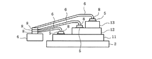
以下、本発明をパワー素子に適用した第1の実施例について、図1ないし図8を参照して説明する。まず、図1は、本実施例の半導体装置1の全体構成を概略的に示す側面図である。この図1に示すように、上記半導体装置1は、アイランド2上に載置固定された半導体チップ3と、リード電極4とから構成されている。上記半導体チップ3は、例えばIGBTやパワーMOSFET等で構成されている。
Hereinafter, a first embodiment in which the present invention is applied to a power element will be described with reference to FIGS. First, FIG. 1 is a side view schematically showing the overall configuration of the
半導体チップ3上に設けられた電極5と、リード電極4との間は、3本のAu線6、6、6をワイヤボンディングすることにより接続されている。
ここで、半導体チップ3の電極5とリード電極4との間を接続するAu線6のワイヤボンディング工程について、図2ないし図8を参照して説明する。まず、半導体チップ3の電極5上にプレボールボンドを実行して、図4に示すように、プレボール7を作成する。
The
Here, the wire bonding process of the
このプレボールボンドは、具体的には、図2及び図3に示すような工程で実行するように構成されている。即ち、図2に示すように、先端にAuボール8が設けられたAu線6をワイヤボンディング用のツール9にセットした後、このツール9を半導体チップ3の電極(パッド)5上に下降させる。続いて、図3に示すように、ツール9によりAuボール8に対して加重と超音波を印加することにより、塑性変形させながら、Auボール8(プレボール7)を電極5に接合する。
Specifically, this pre-ball bond is configured to be executed in a process as shown in FIGS. That is, as shown in FIG. 2, after setting the
そして、ツール9を上昇させることにより、Au線6をプルカットする(図4参照)。この場合、ツール9を設定高さだけ上昇させた後、ツール9を水平方向に移動させると共に、若干下降させることにより、Au線6を押しつぶしながら切断(せん断)するように構成することが好ましい。ここまでの工程が、半導体チップ3上の電極5上にバンプ形状に加工したAuボール8を積み上げる工程に相当する。
Then, the
次に、先端にAuボール8が設けられたAu線6をセットしたツール9をリード電極4上に下降させ、図2及び図3のワイヤボンディング工程と同様にして、リード電極4上にAuボール8を接続する(図5中の左部分参照)。これにより、1回目のボンド(ボールボンド)を完了する。続いて、ツール9を上昇させると共に、水平方向(図5中右方)に移動させて半導体チップ3の電極5の上方に位置させる(このとき、図5に示すように、ツール9の位置を若干右方へずらしておく)。
Next, the
そして、ツール9を下降させることにより、Au線6を半導体チップ3の電極5上にステッチ形状10にて接合して接続する(図6参照)。この後、ツール9を上昇させることにより、Au線6をプルカットする。これにより、2回目のボンド(ステッチボンド)が完了すると共に、図6に示すように、1本目のAu線6のワイヤボンディングの工程が完了する。
Then, by lowering the
ここまでの工程が、積み上げたAuボール8上にリード電極4上のボールボンドを完了したAu線6をステッチボンドして接続する工程に相当する。
続いて、図7(a)、(b)、(c)に示すように、ステッチボンドしたAuボール8上にバンプ形状に加工したAuボール8を積み上げる工程を実行する。具体的には、図7(a)に示すように、先端にAuボール8が設けられたAu線6をセットしたツール9をステッチボンドしたAuボール8上に下降させ、図2及び図3の工程と同様にして、ステッチボンドしたAuボール8上にAuボール8を接合する(図7(b)参照)。これにより、3回目のボンド(ボールボンド)が完了する。
The steps up to here correspond to the steps of connecting the
Subsequently, as shown in FIGS. 7A, 7 </ b> B, and 7 </ b> C, a process of stacking the
続いて、ツール9を上昇させた後(図7(b)参照)、Au線6をプルカットする(図7(c)参照)。この場合も、ツール9を設定高さだけ上昇させた後、ツール9を水平方向に移動させると共に、若干下降させることにより、Au線6を押しつぶしながら切断するように構成している。
次に、上記2段積みしたAuボール8上と、リード電極4上との間に2本目のAu線6をワイヤボンディングする工程を実行する。
Subsequently, after raising the tool 9 (see FIG. 7B), the
Next, a step of wire bonding a
具体的には、まず、先端にAuボール8が設けられたAu線6をセットしたツール9をリード電極4上における2本目のAu線6を接合する部位の上に下降させ、図2及び図3の工程と同様にして、上記リード電極4上にAuボール8を接続する(図8参照)。これにより、3回目のボンド(ボールボンド)が完了する。続いて、ツール9を上昇させると共に、水平方向(図8中右方)に移動させて半導体チップ3の電極5のAuボール8の上方に位置させる(このとき、図8に示すように、ツール9の位置をAuボール8の中心よりも若干右方へずらしておく)。
Specifically, first, the
そして、ツール9を下降させることにより、Au線6を半導体チップ3の電極5上にステッチ形状にて接合して接続する。この後、ツール9を上昇させることにより、Au線6をプルカットする。これにより、4回目のボンド(ステッチボンド)が完了すると共に、2本目のAu線6のワイヤボンディングが完了する。
ここまでの工程が、2重に積み上げたAuボール8上にリード電極4上のボールボンドを完了したAu線6をステッチボンドして接続する工程に相当する。
Then, by lowering the
The process so far corresponds to the process of stitch bonding the
この後、3本目のAu線6をワイヤボンディングするために、上記ステッチボンドしたAuボール8上にバンプ形状に加工したAuボール8(3個目)を積み上げる工程を実行する。この工程は、上述した2個目のAuボール8を積み上げる工程(図7(a)、(b)、(c)参照)とほぼ同様にして実行するように構成されている。そして、上記3段積みしたAuボール8上と、リード電極4上との間に3本目のAu線6をワイヤボンディングする工程を実行する。
Thereafter, in order to wire-bond the
この工程は、上述した2本目のAu線6をワイヤボンディングする工程(図8参照)とほぼ同様にして実行するように構成されている。これにより、3本目のAu線6のワイヤボンディングが完了する。この結果、図1に示す構成の半導体装置1が製造される。
そして、ここまでの工程によって、ステッチボンドしたAuボール8上にバンプ形状に加工したAuボール8を積み上げる工程と、この積み上げたAuボール8上にリード電極4上のボールボンドを完了したAu線6をステッチボンドして接続する工程とを、順に複数回繰り返す製造工程が実現されている。
This step is configured to be executed in substantially the same manner as the step of wire bonding the
Then, by the steps so far, the step of stacking the
このような構成の本実施例によれば、半導体チップ3上の電極5上にAuボールを2個積み上げ、上記1つの電極5上にAu線を2本接続することが可能なように構成したので、半導体チップ3上に設ける電極の個数を少なくすることができ、ひいては、チップサイズを小さくすることができる。そして、チップサイズを小さくできることから、アイランドサイズも小さくすることが可能になる。
According to the present embodiment having such a configuration, two Au balls are stacked on the
更に、上記実施例の場合、2重に積み上げたAuボール8上にリード電極4上のボールボンドを完了したAu線6をステッチボンドして接続する工程を備えるように構成したので、半導体チップ3の1つの電極5上にAu線6を2本接続する構成を実現することができる。
更にまた、上記実施例においては、ステッチボンドしたAuボール8上にバンプ形状に加工したAuボール8を積み上げる工程と、この積み上げたAuボール8上にリード電極4上のボールボンドを完了したAu線6をステッチボンドして接続する工程とを、順に複数回繰り返すように構成したので、半導体チップ3の1つの電極5上にAu線6を3本以上接続する構成を容易に実現することができる。そして、この構成によれば、半導体チップ3上に設ける電極の個数をより一層少なくすることができ、チップサイズを更に一層小さくすることができる。
Further, in the case of the above-described embodiment, since the
Furthermore, in the above embodiment, the
尚、上記実施例においては、半導体チップ3の電極5とリード電極4との間を3本のAu線6でワイヤボンディングするように構成したが、これに限られるものではなく、2本または4本以上のAu線6でワイヤボンディングするように構成しても良い。
In the above embodiment, the wire bonding is performed between the
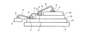
図9は、本発明の第2の実施例を示すものである。尚、第1の実施例と同一構成には、同一符号を付している。この第2の実施例においては、リード電極4上にAuボール8を3段に積み上げ、各Auボール8上に3本のAu線6をそれぞれステッチボンドして接続するように構成した。尚、リード電極4上にAuボール8を3段に積み上げる工程と、各Auボール8上に3本のAu線6をそれぞれステッチボンドする工程は、第1の実施例で実施している各工程とほぼ同様にして実行されるように構成されている。
FIG. 9 shows a second embodiment of the present invention. The same components as those in the first embodiment are denoted by the same reference numerals. In the second embodiment, the
また、半導体チップ3側においては、3本のAu線6は、半導体チップ3上に設けられた3個の電極5上にボールボンドされている。尚、上述した以外の第2の実施例の構成は、第1の実施例の構成と同じ構成となっている。
そして、上記第2の実施例においては、リード電極4上にバンプ形状に加工したAuボール8を積み上げる工程と、積み上げたAuボール8上に、半導体チップ3の電極5上のボールボンドを完了したAu線6をステッチボンドして接続する工程と、ステッチボンドしたAuボール8上にバンプ形状に加工したAuボール8を積み上げる工程と、2重に積み上げたAuボール8上に、半導体チップ3の電極5上のボールボンドを完了したAu線6をステッチボンドして接続する工程とが実行されるように構成されている。
On the
And in the said 2nd Example, the process of piling up the
更に、上記実施例では、上記ステッチボンドしたAuボール8上にバンプ形状に加工したAuボール8を積み上げる工程と、この積み上げたAuボール8上に、半導体チップ3の電極5上のボールボンドを完了したAu線6をステッチボンドして接続する工程とを、順に複数回繰り返す製造工程が実行される構成となっている。
また、上記第2の実施例によれば、3本のAu線6をリード電極4上の1ヶ所の部位に接続するように構成したので、リード電極4のサイズを小さくすることができる。
Further, in the above embodiment, the process of stacking the
According to the second embodiment, since the three
図10は、本発明の第3の実施例を示すものである。尚、第2の実施例と同一構成には、同一符号を付している。この第3の実施例においては、アイランド2上に第1の半導体チップ11を載置して固着すると共に、この第1の半導体チップ11上に、これよりもサイズが小さい第2の半導体チップ12を載置して固着し、更に、この第2の半導体チップ12上に、これよりもサイズが小さい第3の半導体チップ13を載置して固着している。即ち、3つの半導体チップ11、12、13は、スタック構造となるように構成されている。
FIG. 10 shows a third embodiment of the present invention. The same components as those in the second embodiment are denoted by the same reference numerals. In the third embodiment, the
そして、リード電極4上に積み上げた最下段のAuボール8と、第1の半導体チップ11上における第2の半導体チップ12が載置されていない部分に設けられた電極5とが、1本目のAu線6でワイヤボンディングされている。また、リード電極4上に積み上げた2番目のAuボール8と、第2の半導体チップ12上における第3の半導体チップ13が載置されていない部分に設けられた電極5とが、2本目のAu線6でワイヤボンディングされている。更に、リード電極4上に積み上げた最上段のAuボール8と、第3の半導体チップ13上に設けられた電極5とが、3本目のAu線6でワイヤボンディングされている。
The
尚、上述した以外の第3の実施例の構成は、第2の実施例の構成と同じ構成となっている。従って、第3の実施例においても、第2の実施例とほぼ同じ作用効果を得ることができる。
また、上記第3の実施例においては、アイランド2上に3つの半導体チップ11、12、13を積み重ねるように構成したが、これに限られるものではなく、2個または4個以上の半導体チップを積み重ねるように構成しても良い。
The configuration of the third embodiment other than that described above is the same as that of the second embodiment. Accordingly, in the third embodiment, substantially the same operational effects as in the second embodiment can be obtained.
In the third embodiment, the three
図11は、本発明の第4の実施例を示すものである。尚、第2の実施例と同一構成には、同一符号を付している。この第4の実施例においては、アイランド2上に例えば3個の半導体チップ14、14、14を並べて載置して固着している。即ち、上記第4の時の場合、3個の半導体チップ14、14、14は、マルチチップ構造なるように構成されている。そして、リード電極4上に積み上げた最下段のAuボール8と、図11中の左端の半導体チップ14上に設けられた電極5とが、1本目のAu線6でワイヤボンディングされている。
FIG. 11 shows a fourth embodiment of the present invention. The same components as those in the second embodiment are denoted by the same reference numerals. In the fourth embodiment, for example, three
また、リード電極4上に積み上げた2番目のAuボール8と、図11中の中央の半導体チップ14上に設けられた電極5とが、2本目のAu線6でワイヤボンディングされている。更に、リード電極4上に積み上げた最上段のAuボール8と、図11中の右端の半導体チップ14上に設けられた電極5とが、3本目のAu線6でワイヤボンディングされている。
Further, the
尚、上述した以外の第4の実施例の構成は、第2の実施例の構成と同じ構成となっている。従って、第4の実施例においても、第2の実施例とほぼ同じ作用効果を得ることができる。
また、上記第4の実施例においては、アイランド2上に3つの半導体チップ3を並べて配置するように構成したが、これに限られるものではなく、2個または4個以上の半導体チップを並べて配置するように構成しても良い。
The configuration of the fourth embodiment other than that described above is the same as the configuration of the second embodiment. Accordingly, in the fourth embodiment, substantially the same operational effects as in the second embodiment can be obtained.
In the fourth embodiment, the three
図12は、本発明の第5の実施例を示すものである。尚、第3の実施例と同一構成には、同一符号を付している。この第5の実施例においては、アイランド2上に3つの半導体チップ11、12、13をスタック構造となるように構成している。そして、第1の半導体チップ11上における第2の半導体チップ12が載置されていない部分に設けられた電極5上に、2個のAuボール8を積み上げている。更に、第2の半導体チップ12上における第3の半導体チップ13が載置されていない部分に設けられた電極5上に、3個のAuボール8を積み上げている。
FIG. 12 shows a fifth embodiment of the present invention. The same components as those in the third embodiment are denoted by the same reference numerals. In the fifth embodiment, three
そして、リード電極4上と、第1の半導体チップ11の電極5上に積み上げた下段のAuボール8とが、1本目のAu線6でワイヤボンディングされている。また、第1の半導体チップ11の電極5上に積み上げた上段のAuボール8と、第2の半導体チップ12の電極5上に積み上げた最下段のAuボール8とが、2本目のAu線6でワイヤボンディングされている。更に、第2の半導体チップ12上に積み上げた最上段のAuボール8と、第3の半導体チップ13上に設けられた電極5とが、3本目のAu線6でワイヤボンディングされている。
The
尚、上述した以外の第5の実施例の構成は、第3の実施例の構成と同じ構成となっている。従って、第5実施例においても、第3の実施例とほぼ同じ作用効果を得ることができる。特に、第5の実施例においては、第1の半導体チップ11の電極5上に2個のAuボール8を積み上げると共に、第2の半導体チップ12の電極5上に3個のAuボール8を積み上げるように構成したので、Au線6が半導体チップ12、13のエッジ部に接触して機能不良を起こすことを防止することができる。これにより、半導体チップ11、12、13上における電極5の配置の設計自由度を高くすることができる。
The configuration of the fifth embodiment other than that described above is the same as that of the third embodiment. Therefore, in the fifth embodiment, substantially the same operational effects as in the third embodiment can be obtained. In particular, in the fifth embodiment, two
図13は、本発明の第6の実施例を示すものである。尚、第4の実施例と同一構成には、同一符号を付している。この第6の実施例においては、2個の半導体チップ3を2個のアイランド2の上にそれぞれ設けると共に、2個の半導体チップ3の間にリード電極4を配置するように構成した。そして、リード電極4上に2個のAuボール8を積み上げ、このうちの、下段のAuボール8上に、図13中左の半導体チップ3上に設けられた3個の電極5上にそれぞれボールボンドされた3本のAu線6をステッチボンドしている。
FIG. 13 shows a sixth embodiment of the present invention. The same components as those in the fourth embodiment are denoted by the same reference numerals. In the sixth embodiment, the two
更に、リード電極4上に積み上げられた上段のAuボール8上に、図13中右の半導体チップ3上に設けられた3個の電極5上にそれぞれボールボンドされた3本のAu線6をステッチボンドしている。尚、上述した以外の第6の実施例の構成は、第4の実施例の構成と同じ構成となっている。従って、第6実施例においても、第4の実施例とほぼ同じ作用効果を得ることができる。特に、第6の実施例においては、6本のAu線6をリード電極4上の1つの箇所に接合するように構成したので、リード電極4のサイズを小さくすることができる。
Further, on the
尚、上記第6の実施例においては、リード電極4上に2個のAuボール8を積み上げるように構成したが、これに限られるものではなく、リード電極4上に6個のAuボール8を積み上げ、各Auボール8上にAu線6を1本ずつステッチボンドするように構成しても良い。
In the sixth embodiment, the two
図14は、本発明の第7の実施例を示すものである。尚、第4の実施例と同一構成には、同一符号を付している。この第7の実施例においては、2個の半導体チップ3をアイランド2の上下面に固着する、即ち、両面実装するように構成している。
FIG. 14 shows a seventh embodiment of the present invention. The same components as those in the fourth embodiment are denoted by the same reference numerals. In the seventh embodiment, the two
具体的には、アイランド2の上下面に半導体チップ3、3をそれぞれ実装し、リード電極4の上下面にそれぞれ3個のAuボール8を積み上げている。そして、リード電極4の上面に設けられた3個のAuボール8上に、アイランド2の上面に実装された半導体チップ3上に設けられた3個の電極5上にそれぞれボールボンドされた3本のAu線6をそれぞれステッチボンドしている。
Specifically, the
また、リード電極4の下面に設けられた3個のAuボール8上に、アイランド2の下面に実装された半導体チップ3上に設けられた3個の電極5上にそれぞれボールボンドされた3本のAu線6をそれぞれステッチボンドしている。上述した以外の第7の実施例の構成は、第4の実施例の構成と同じ構成となっている。従って、第7実施例においても、第4の実施例とほぼ同じ作用効果を得ることができる。特に、第7の実施例においては、2個の半導体チップ3をアイランド2に両面実装するように構成したので、アイランド2及びリード電極4の各サイズを小さくすることができる。
Also, three balls bonded to the three
図面中、1は半導体装置、2はアイランド、3は半導体チップ、4はリード電極、5は電極、6はAu線、7はプレボール、8はAuボール、11は第1の半導体チップ、12は第2の半導体チップ、13は第3の半導体チップ、14は半導体チップを示す。 In the drawings, 1 is a semiconductor device, 2 is an island, 3 is a semiconductor chip, 4 is a lead electrode, 5 is an electrode, 6 is an Au wire, 7 is a preball, 8 is an Au ball, 11 is a first semiconductor chip, 12 is The second semiconductor chip, 13 is a third semiconductor chip, and 14 is a semiconductor chip.
Claims (11)
前記積み上げたAuボール上にリード電極上のボールボンドを完了したAu線をステッチボンドして接続する工程と、
前記ステッチボンドしたAuボール上にバンプ形状に加工したAuボールを積み上げる工程とを備えたことを特徴とする半導体装置の製造方法。 A process of stacking Au balls processed into bump shapes on electrodes on a semiconductor chip;
Stitching and connecting the Au wires that have completed the ball bonding on the lead electrodes on the stacked Au balls; and
And a step of stacking Au balls processed into a bump shape on the stitch-bonded Au balls.
この積み上げたAuボール上に、リード電極上のボールボンドを完了したAu線をステッチボンドして接続する工程とを、順に複数回繰り返すことを特徴とする請求項1記載の半導体装置の製造方法。 A process of stacking Au balls processed into a bump shape on the stitch bonded Au balls;
2. The method of manufacturing a semiconductor device according to claim 1, wherein the step of stitch bonding the Au wires that have completed the ball bonding on the lead electrodes to the stacked Au balls is repeated a plurality of times in order.
前記積み上げたAuボール上に、半導体チップの電極上のボールボンドを完了したAu線をステッチボンドして接続する工程と、
前記ステッチボンドしたAuボール上にバンプ形状に加工したAuボールを積み上げる工程とを備えたことを特徴とする半導体装置の製造方法。 A process of stacking Au balls processed into a bump shape on the lead electrode;
A step of stitch-bonding and connecting Au wires that have completed ball bonding on the electrodes of the semiconductor chip on the stacked Au balls;
And a step of stacking Au balls processed into a bump shape on the stitch-bonded Au balls.
この積み上げたAuボール上に、半導体チップの電極上のボールボンドを完了したAu線をステッチボンドして接続する工程とを、順に複数回繰り返すことを特徴とする請求項4記載の半導体装置の製造方法。 A process of stacking Au balls processed into a bump shape on the stitch bonded Au balls;
5. The method of manufacturing a semiconductor device according to claim 4, wherein the step of stitching and connecting the Au wires having completed the ball bonding on the electrodes of the semiconductor chip to the stacked Au balls is repeated a plurality of times in order. Method.
リード電極とを備え、
前記半導体チップの電極上にバンプ形状に加工したAuボールを積み上げ、この積み上げたAuボール上に、リード電極上のボールボンドを完了したAu線をステッチボンドして接続し、このステッチボンドしたAuボール上にバンプ形状に加工したAuボールを積み上げ、更に、この積み上げたAuボール上に、リード電極上のボールボンドを完了したAu線をステッチボンドして接続するように構成したことを特徴とする半導体装置。 A semiconductor chip;
With lead electrodes,
Au balls processed into bump shapes are stacked on the electrodes of the semiconductor chip, and Au wires that have completed ball bonding on the lead electrodes are connected to the stacked Au balls by stitch bonding, and the stitch bonded Au balls An Au ball processed into a bump shape is stacked on top of the Au ball, and a Au wire that has completed ball bonding on the lead electrode is connected to the stacked Au ball by stitch bonding. apparatus.
リード電極とを備え、
前記リード電極上にバンプ形状に加工したAuボールを積み上げ、この積み上げたAuボール上に、前記半導体チップの1つの電極上のボールボンドを完了したAu線をステッチボンドして接続し、このステッチボンドしたAuボール上にバンプ形状に加工したAuボールを積み上げ、更に、この積み上げたAuボール上に、前記半導体チップの他の電極上のボールボンドを完了したAu線をステッチボンドして接続するように構成したことを特徴とする半導体装置。 A semiconductor chip;
With lead electrodes,
Au balls processed into a bump shape are stacked on the lead electrodes, and Au wires that have completed ball bonding on one electrode of the semiconductor chip are connected to the stacked Au balls by stitch bonding. Au balls processed into bumps are stacked on the Au balls, and Au wires that have completed ball bonding on the other electrodes of the semiconductor chip are connected to the stacked Au balls by stitch bonding. A semiconductor device characterized by comprising.
このアイランド上に第1の半導体チップを載置すると共に、
この第1の半導体チップ上に第2の半導体チップを載置し、
前記第1の半導体チップ上における前記第2の半導体チップが載置されていない部分に設けられた電極を前記1つの電極とし、
前記第2の半導体チップ上に設けられた電極を前記他の電極とするように構成したことを特徴とする請求項8記載の半導体装置。 Equipped with an island to place semiconductor chips,
While placing the first semiconductor chip on this island,
A second semiconductor chip is mounted on the first semiconductor chip;
An electrode provided on a portion of the first semiconductor chip where the second semiconductor chip is not placed is the one electrode,
9. The semiconductor device according to claim 8, wherein an electrode provided on the second semiconductor chip is used as the other electrode.
このアイランド上に複数の半導体チップを並べて載置し、
前記複数の半導体チップのうちの1つの半導体チップ上に設けられた電極を前記1つの電極とし、
前記複数の半導体チップのうちの他の1つの半導体チップ上に設けられた電極を前記他の電極とするように構成したことを特徴とする請求項8記載の半導体装置。 Equipped with an island to place semiconductor chips,
A plurality of semiconductor chips are placed side by side on this island,
The electrode provided on one semiconductor chip of the plurality of semiconductor chips is the one electrode,
9. The semiconductor device according to claim 8, wherein an electrode provided on another one of the plurality of semiconductor chips is configured as the other electrode.
このアイランド上に複数の半導体チップを積み重ねて載置し、
前記複数の半導体チップのうちの1つの半導体チップ上における他の半導体チップが載置されていない部分に設けられた電極上に、複数のAuボールを積み上げるように構成し、これら複数の積み上げたAuボールのうちの1つのAuボール上に、リード電極上のボールボンドを完了したAu線、または、他の半導体チップの電極上のボールボンドを完了したAu線をステッチボンドして接続するように構成したことを特徴とする請求項7記載の半導体装置。
Equipped with an island to place semiconductor chips,
A plurality of semiconductor chips are stacked and placed on this island,
A plurality of Au balls are stacked on an electrode provided on a portion of the plurality of semiconductor chips where no other semiconductor chip is placed, and the plurality of stacked Au Configured to connect the Au wire that has completed the ball bond on the lead electrode or the Au wire that has completed the ball bond on the electrode of another semiconductor chip by stitch bonding to one Au ball of the balls 8. The semiconductor device according to claim 7, wherein:
Priority Applications (4)
| Application Number | Priority Date | Filing Date | Title |
|---|---|---|---|
| JP2004078244A JP2005268497A (en) | 2004-03-18 | 2004-03-18 | Semiconductor device and manufacturing method of semiconductor device |
| US11/063,866 US7285854B2 (en) | 2004-03-18 | 2005-02-24 | Wire bonding method and semiconductor device |
| DE102005011429A DE102005011429A1 (en) | 2004-03-18 | 2005-03-11 | Wire bonding method and semiconductor device |
| CNB200510054299XA CN100361285C (en) | 2004-03-18 | 2005-03-18 | Wire bonding method and semiconductor device |
Applications Claiming Priority (1)
| Application Number | Priority Date | Filing Date | Title |
|---|---|---|---|
| JP2004078244A JP2005268497A (en) | 2004-03-18 | 2004-03-18 | Semiconductor device and manufacturing method of semiconductor device |
Publications (1)
| Publication Number | Publication Date |
|---|---|
| JP2005268497A true JP2005268497A (en) | 2005-09-29 |
Family
ID=34980797
Family Applications (1)
| Application Number | Title | Priority Date | Filing Date |
|---|---|---|---|
| JP2004078244A Pending JP2005268497A (en) | 2004-03-18 | 2004-03-18 | Semiconductor device and manufacturing method of semiconductor device |
Country Status (4)
| Country | Link |
|---|---|
| US (1) | US7285854B2 (en) |
| JP (1) | JP2005268497A (en) |
| CN (1) | CN100361285C (en) |
| DE (1) | DE102005011429A1 (en) |
Cited By (5)
| Publication number | Priority date | Publication date | Assignee | Title |
|---|---|---|---|---|
| JP2008034567A (en) * | 2006-07-27 | 2008-02-14 | Fujitsu Ltd | Semiconductor device and manufacturing method thereof |
| JP2008288229A (en) * | 2007-05-15 | 2008-11-27 | Citizen Electronics Co Ltd | Light emitting diode and manufacturing method thereof |
| JP2009124075A (en) * | 2007-11-19 | 2009-06-04 | Denso Corp | Wire bonding method and wire bonding structure |
| JP2010238946A (en) * | 2009-03-31 | 2010-10-21 | Sanyo Electric Co Ltd | Semiconductor device and manufacturing method thereof |
| CN111933605A (en) * | 2020-08-10 | 2020-11-13 | 紫光宏茂微电子(上海)有限公司 | Chip welding structure and welding method |
Families Citing this family (34)
| Publication number | Priority date | Publication date | Assignee | Title |
|---|---|---|---|---|
| JP4427298B2 (en) * | 2003-10-28 | 2010-03-03 | 富士通株式会社 | Multi-step bump formation method |
| US8138080B2 (en) * | 2006-03-10 | 2012-03-20 | Stats Chippac Ltd. | Integrated circuit package system having interconnect stack and external interconnect |
| TWI293502B (en) * | 2006-03-16 | 2008-02-11 | Advanced Semiconductor Eng | Chip package structure |
| US20070216026A1 (en) * | 2006-03-20 | 2007-09-20 | Adams Zhu | Aluminum bump bonding for fine aluminum wire |
| US7772045B1 (en) * | 2006-10-24 | 2010-08-10 | Randy Wayne Bindrup | Wire bond method for angularly disposed conductive pads and a device made from the method |
| JP2008117888A (en) * | 2006-11-02 | 2008-05-22 | Rohm Co Ltd | Electronic component and wire bonding method |
| JP5481769B2 (en) * | 2006-11-22 | 2014-04-23 | 日亜化学工業株式会社 | Semiconductor device and manufacturing method thereof |
| US20080246129A1 (en) * | 2007-04-04 | 2008-10-09 | Matsushita Electric Industrial Co., Ltd. | Method of manufacturing semiconductor device and semiconductor device |
| SG150395A1 (en) * | 2007-08-16 | 2009-03-30 | Micron Technology Inc | Stacked microelectronic devices and methods for manufacturing stacked microelectronic devices |
| US8247272B2 (en) * | 2007-12-27 | 2012-08-21 | United Test And Assembly Center Ltd. | Copper on organic solderability preservative (OSP) interconnect and enhanced wire bonding process |
| EP2133915A1 (en) * | 2008-06-09 | 2009-12-16 | Micronas GmbH | Semiconductor assembly with specially formed bonds and method for manufacturing the same |
| CN101615587A (en) * | 2008-06-27 | 2009-12-30 | 桑迪士克股份有限公司 | Wire-stack stitch bonding in semiconductor devices |
| JP5595694B2 (en) * | 2009-01-15 | 2014-09-24 | パナソニック株式会社 | Semiconductor device |
| JP5062283B2 (en) | 2009-04-30 | 2012-10-31 | 日亜化学工業株式会社 | Semiconductor device and manufacturing method thereof |
| US8008785B2 (en) | 2009-12-22 | 2011-08-30 | Tessera Research Llc | Microelectronic assembly with joined bond elements having lowered inductance |
| TWI409933B (en) * | 2010-06-15 | 2013-09-21 | 力成科技股份有限公司 | Chip stacked package structure and its fabrication method |
| US8357563B2 (en) * | 2010-08-10 | 2013-01-22 | Spansion Llc | Stitch bump stacking design for overall package size reduction for multiple stack |
| CN101996907B (en) * | 2010-09-09 | 2012-04-18 | 上海微松工业自动化有限公司 | Bumping device for pressing wafer-level elastomer into microsphere |
| WO2012055085A1 (en) * | 2010-10-26 | 2012-05-03 | 上海嘉塘电子有限公司 | Method for bonding wire between chips or between chip and metal frame |
| CN102820236B (en) * | 2011-06-08 | 2015-08-26 | 无锡华润安盛科技有限公司 | A kind of wire bonding method of pre-plastic package lead frame |
| US8791007B2 (en) * | 2011-11-29 | 2014-07-29 | Spansion Llc | Device having multiple wire bonds for a bond area and methods thereof |
| KR20130104430A (en) * | 2012-03-14 | 2013-09-25 | 삼성전자주식회사 | Multi-chip package and method of manufacturing the same |
| KR20140011687A (en) * | 2012-07-18 | 2014-01-29 | 삼성전자주식회사 | Semiconductor package and method for fabricating the same |
| CN103000543A (en) * | 2012-12-18 | 2013-03-27 | 可天士半导体(沈阳)有限公司 | High-reliability bonding method |
| US20140374151A1 (en) * | 2013-06-24 | 2014-12-25 | Jia Lin Yap | Wire bonding method for flexible substrates |
| CN105845655B (en) * | 2016-03-24 | 2018-05-04 | 中国电子科技集团公司第二十九研究所 | Superposition carries out the method and microbonding disk superposition bonding structure of ball-shaped welded on microbonding disk |
| US11373974B2 (en) | 2016-07-01 | 2022-06-28 | Intel Corporation | Electronic device packages and methods for maximizing electrical current to dies and minimizing bond finger size |
| JP2018110169A (en) * | 2016-12-28 | 2018-07-12 | 富士電機株式会社 | Semiconductor device and manufacturing method for semiconductor device |
| US10600756B1 (en) * | 2017-02-15 | 2020-03-24 | United States Of America, As Represented By The Secretary Of The Navy | Wire bonding technique for integrated circuit board connections |
| CN108610028B (en) * | 2018-05-21 | 2021-04-23 | 潮州三环(集团)股份有限公司 | A ceramic chopper |
| KR102736238B1 (en) * | 2020-01-10 | 2024-12-02 | 에스케이하이닉스 주식회사 | Semiconductor package including bonding wire branch structure |
| US20230275060A1 (en) * | 2022-02-28 | 2023-08-31 | Texas Instruments Incorporated | Leaded semiconductor package with lead mold flash reduction |
| US12394745B2 (en) | 2022-04-21 | 2025-08-19 | Semiconductor Components Industries, Llc | Semiconductor device including bonding covers |
| CN115763284A (en) * | 2022-12-24 | 2023-03-07 | 西安微电子技术研究所 | A wire bonding method for improving the current passing through a single pad of a chip |
Family Cites Families (14)
| Publication number | Priority date | Publication date | Assignee | Title |
|---|---|---|---|---|
| JP3344235B2 (en) | 1996-10-07 | 2002-11-11 | 株式会社デンソー | Wire bonding method |
| JPH10229100A (en) | 1997-02-17 | 1998-08-25 | Tokai Rika Co Ltd | Wire bonding method and plastic package manufacturing method |
| JPH11233543A (en) | 1998-02-13 | 1999-08-27 | Sumitomo Metal Mining Co Ltd | Method of forming bump and electronic component with bump |
| JP3378809B2 (en) | 1998-09-30 | 2003-02-17 | 三洋電機株式会社 | Semiconductor device |
| JP3869562B2 (en) | 1998-10-16 | 2007-01-17 | 三洋電機株式会社 | Manufacturing method of semiconductor device |
| JP3662461B2 (en) | 1999-02-17 | 2005-06-22 | シャープ株式会社 | Semiconductor device and manufacturing method thereof |
| JP3765952B2 (en) * | 1999-10-19 | 2006-04-12 | 富士通株式会社 | Semiconductor device |
| JP3631120B2 (en) * | 2000-09-28 | 2005-03-23 | 沖電気工業株式会社 | Semiconductor device |
| JP3913134B2 (en) * | 2002-08-08 | 2007-05-09 | 株式会社カイジョー | Bump forming method and bump |
| JP3727272B2 (en) * | 2002-01-15 | 2005-12-14 | 沖電気工業株式会社 | Semiconductor device and manufacturing method of semiconductor device |
| JP3584930B2 (en) | 2002-02-19 | 2004-11-04 | セイコーエプソン株式会社 | Semiconductor device and manufacturing method thereof, circuit board, and electronic apparatus |
| JP3935370B2 (en) | 2002-02-19 | 2007-06-20 | セイコーエプソン株式会社 | Bumped semiconductor element manufacturing method, semiconductor device and manufacturing method thereof, circuit board, and electronic device |
| JP3573133B2 (en) * | 2002-02-19 | 2004-10-06 | セイコーエプソン株式会社 | Semiconductor device and its manufacturing method, circuit board, and electronic equipment |
| US20030230796A1 (en) * | 2002-06-12 | 2003-12-18 | Aminuddin Ismail | Stacked die semiconductor device |
-
2004
- 2004-03-18 JP JP2004078244A patent/JP2005268497A/en active Pending
-
2005
- 2005-02-24 US US11/063,866 patent/US7285854B2/en not_active Expired - Lifetime
- 2005-03-11 DE DE102005011429A patent/DE102005011429A1/en not_active Withdrawn
- 2005-03-18 CN CNB200510054299XA patent/CN100361285C/en not_active Expired - Fee Related
Cited By (6)
| Publication number | Priority date | Publication date | Assignee | Title |
|---|---|---|---|---|
| JP2008034567A (en) * | 2006-07-27 | 2008-02-14 | Fujitsu Ltd | Semiconductor device and manufacturing method thereof |
| US8134240B2 (en) | 2006-07-27 | 2012-03-13 | Fujitsu Semiconductor Limited | Semiconductor device and manufacturing method for the same |
| JP2008288229A (en) * | 2007-05-15 | 2008-11-27 | Citizen Electronics Co Ltd | Light emitting diode and manufacturing method thereof |
| JP2009124075A (en) * | 2007-11-19 | 2009-06-04 | Denso Corp | Wire bonding method and wire bonding structure |
| JP2010238946A (en) * | 2009-03-31 | 2010-10-21 | Sanyo Electric Co Ltd | Semiconductor device and manufacturing method thereof |
| CN111933605A (en) * | 2020-08-10 | 2020-11-13 | 紫光宏茂微电子(上海)有限公司 | Chip welding structure and welding method |
Also Published As
| Publication number | Publication date |
|---|---|
| US20050205995A1 (en) | 2005-09-22 |
| CN1670935A (en) | 2005-09-21 |
| DE102005011429A1 (en) | 2005-10-06 |
| CN100361285C (en) | 2008-01-09 |
| US7285854B2 (en) | 2007-10-23 |
Similar Documents
| Publication | Publication Date | Title |
|---|---|---|
| JP2005268497A (en) | Semiconductor device and manufacturing method of semiconductor device | |
| US8134240B2 (en) | Semiconductor device and manufacturing method for the same | |
| US10153247B2 (en) | Methods of forming wire interconnect structures | |
| US7044357B2 (en) | Bump formation method and wire bonding method | |
| JP2002280414A (en) | Semiconductor device and method of manufacturing the same | |
| JP2000307057A (en) | Semiconductor device and method of manufacturing the same | |
| JP2013539213A (en) | Stitch bump stacking design for multi-stack overall package size reduction | |
| JP2008103685A (en) | Semiconductor device and manufacturing method thereof | |
| JP2008277751A (en) | Semiconductor device manufacturing method and semiconductor device | |
| CN1946504A (en) | System and method for low loop wire bonding | |
| JP2005159267A (en) | Semiconductor device and wire bonding method | |
| JP5018420B2 (en) | Wire bonding method and wire bonding structure | |
| JP2010087403A (en) | Semiconductor device | |
| US20060001157A1 (en) | Methods and apparatus for integrated circuit ball bonding using stacked ball bumps | |
| JP2823000B2 (en) | Wire bonding method | |
| JP2007214238A (en) | Semiconductor device and manufacturing method thereof | |
| US20250286012A1 (en) | Semiconductor package having a ball-bond interconnect structure and related methods of manufacturing | |
| JP2010073747A (en) | Wire bonding method and semiconductor device | |
| JP2005051038A (en) | Semiconductor device and manufacturing method thereof | |
| JP2006108408A (en) | Semiconductor device and manufacturing method thereof | |
| CN101170104B (en) | Stacked chip packaging structure with multi-section bus bar in lead frame | |
| JP5048990B2 (en) | Semiconductor device and manufacturing method thereof | |
| KR20070062084A (en) | Bump reverse stitch bonding method, chip stack structure and chip stack method using the same | |
| JP2005353908A (en) | Stack mounting structure | |
| JP2007115981A (en) | Semiconductor device |
Legal Events
| Date | Code | Title | Description |
|---|---|---|---|
| A621 | Written request for application examination |
Free format text: JAPANESE INTERMEDIATE CODE: A621 Effective date: 20060515 |
|
| A977 | Report on retrieval |
Free format text: JAPANESE INTERMEDIATE CODE: A971007 Effective date: 20071221 |
|
| A131 | Notification of reasons for refusal |
Free format text: JAPANESE INTERMEDIATE CODE: A131 Effective date: 20080108 |
|
| A02 | Decision of refusal |
Free format text: JAPANESE INTERMEDIATE CODE: A02 Effective date: 20080430 |